 | –≠–ª–µ–∫—Ç—Ä–æ–Ω–Ω—ã–π –∫–æ–º–ø–æ–Ω–µ–Ω—Ç: Z86C32 | –°–∫–∞—á–∞—Ç—å:  PDF PDF  ZIP ZIP |

CP96DZ82900
1
Z86C30/C31/C32/C40
CP96DZ82900
Z
ILOG
FEATURES
ROM
RAM*
Speed
Part
(KB)
(Byte)
(MHz)
Z86C30
4
237
16
Z86C31
2
125
12
Z86C32
2
237
12
Z86C40
4
236
16
* General-Purpose
s
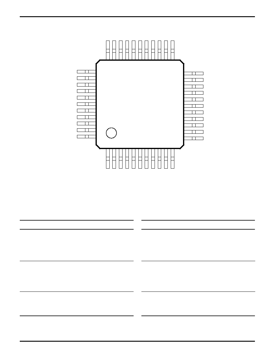
28-Pin DIP, 28-Pin SOIC, 28-Pin PLCC Packages
(Z86C3X)
40-Pin DIP, 44-Pin PLCC/QFP Packages (Z86C40)
s
3.0V to 5.5V Operating Range
s
Low-Power Consumption
s
≠40
∞
C to +105
∞
C Operating Range
s
Expanded Register File (ERF)
s
32 Input/Output Lines (C40)
24 Input/Output Lines (C3X)
s
Vectored, Prioritized Interrupts with
Programmable Polarity
s
Two Analog Comparators
s
Two Programmable 8-Bit Counter/Timers,
Each with Two 6-Bit Programmable Prescaler
s
Watch-Dog Timer/Power-On Reset
s
On-Chip Oscillator that Accepts a Crystal, Ceramic
Resonator, LC, RC, or External Clock
s
RAM and ROM Protect
Z86C30/C31/C32/C40
CMOS Z8
Æ
C
ONSUMER
C
ONTROLLER
P
ROCESSOR
The Z86C3X/C40 Consumer Controller Processors
(CCP) are members of the Z8
Æ
single-chip microcontroller
family offering a unique register-to-register architecture
that avoids accumulator bottlenecks and offers fast execu-
tion of code.
Three address spaces (Program Memory, Register File,
and Expanded Register File [ERF]), support a wide range
of memory configurations. Through the ERF, the designer
has access to three additional control registers that pro-
vide extra peripheral devices, I/O ports, and
register addresses. The rest of the ERF is not physically
implemented and is open for future expansion.
For applications demanding powerful I/O capabilities, the
Z86C3X/C40's dedicated input and output lines are
grouped into three and four ports, respectively, and are
configurable under software control to provide timing,
status signals, or parallel I/O.
Two on-chip counter/timers, with a large number of select-
able modes, offload the system of administering real-time
tasks such as counting/timing and I/O data communica-
tions.
With ROM/ROMless selectivity, the Z86C40 provides both
external memory and pre-programmed ROM, which
enables these Z8 microcontrollers to be used in high-
volume applications, or where code flexibility is required.
Notes:
All Signals with a preceding front slash, "/", are active Low, e.g.:
B//W (WORD is active Low); /B/W (BYTE is active Low, only).
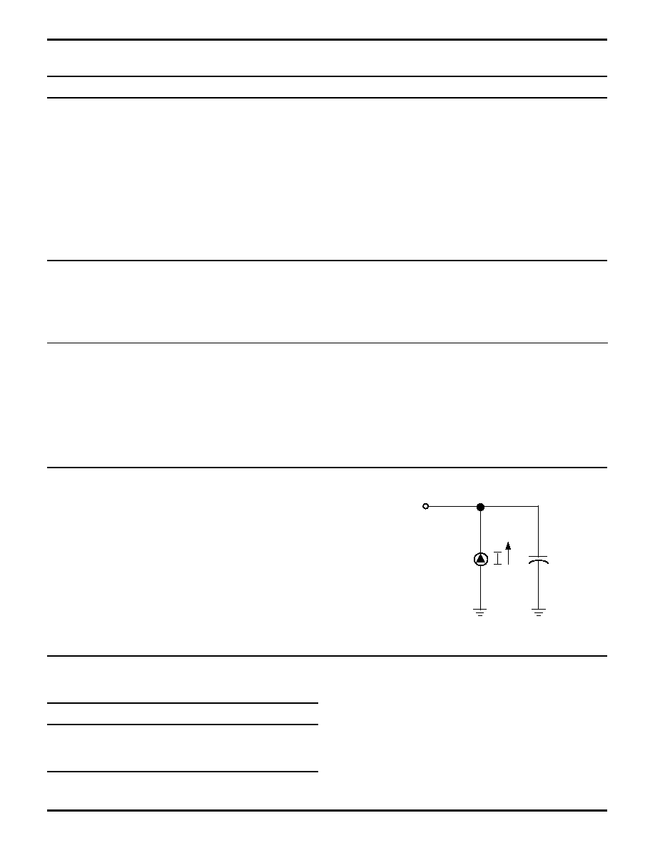
Power connections follow conventional descriptions below:
Connection
Circuit
Device
Power
V
CC
V
DD
Ground
GND
V
SS
GENERAL DESCRIPTION
P
RELIMINARY
C
USTOMER
P
ROCUREMENT
S
PECIFICATION
2
CP96DZ82900
Z86C30/C31/C32/C40
CP96DZ82900
Z
ILOG
GENERAL DESCRIPTION
(Continued)
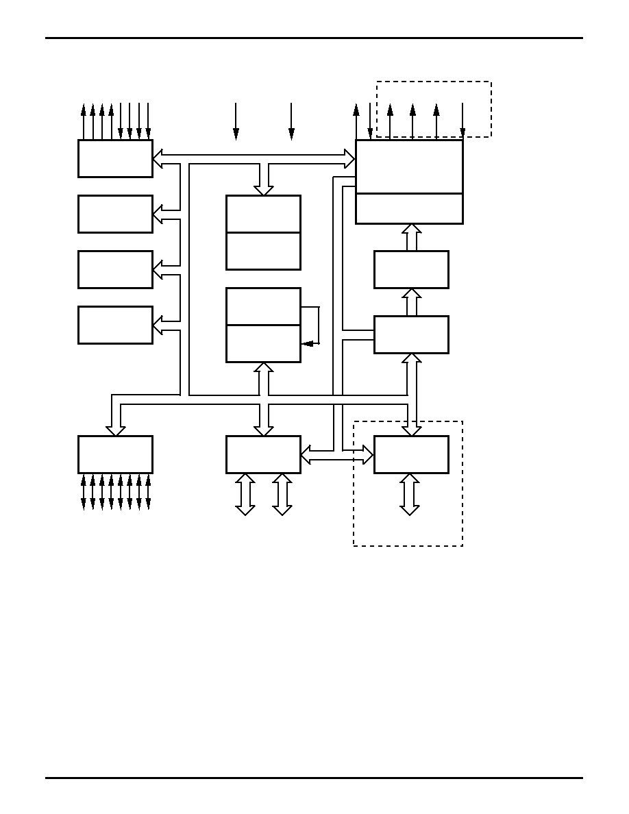
Port 3
Counter/
Timers (2)
Interrupt
Control
Two Analog
Comparators
Port 2
I/O
(Bit Programmable)
ALU
FLAGS
Register
Pointer
Register File
Machine Timing
&
Instruction Control
Prg. Memory
4K
Program
Counter
Vcc
GND
XTAL
4
4
Port 0
Output
Input
Address or I/O
(Nibble Programmable)
8
Port 1
Address/Data or I/O
(Byte Programmable)
/AS /DS R//W /RESET
RESET
WDT, POR
(Only on Z86C40)
(Only on Z86C40)
Functional Block Diagram
CP96DZ82900
3
Z86C30/C31/C32/C40
CP96DZ82900
Z
ILOG
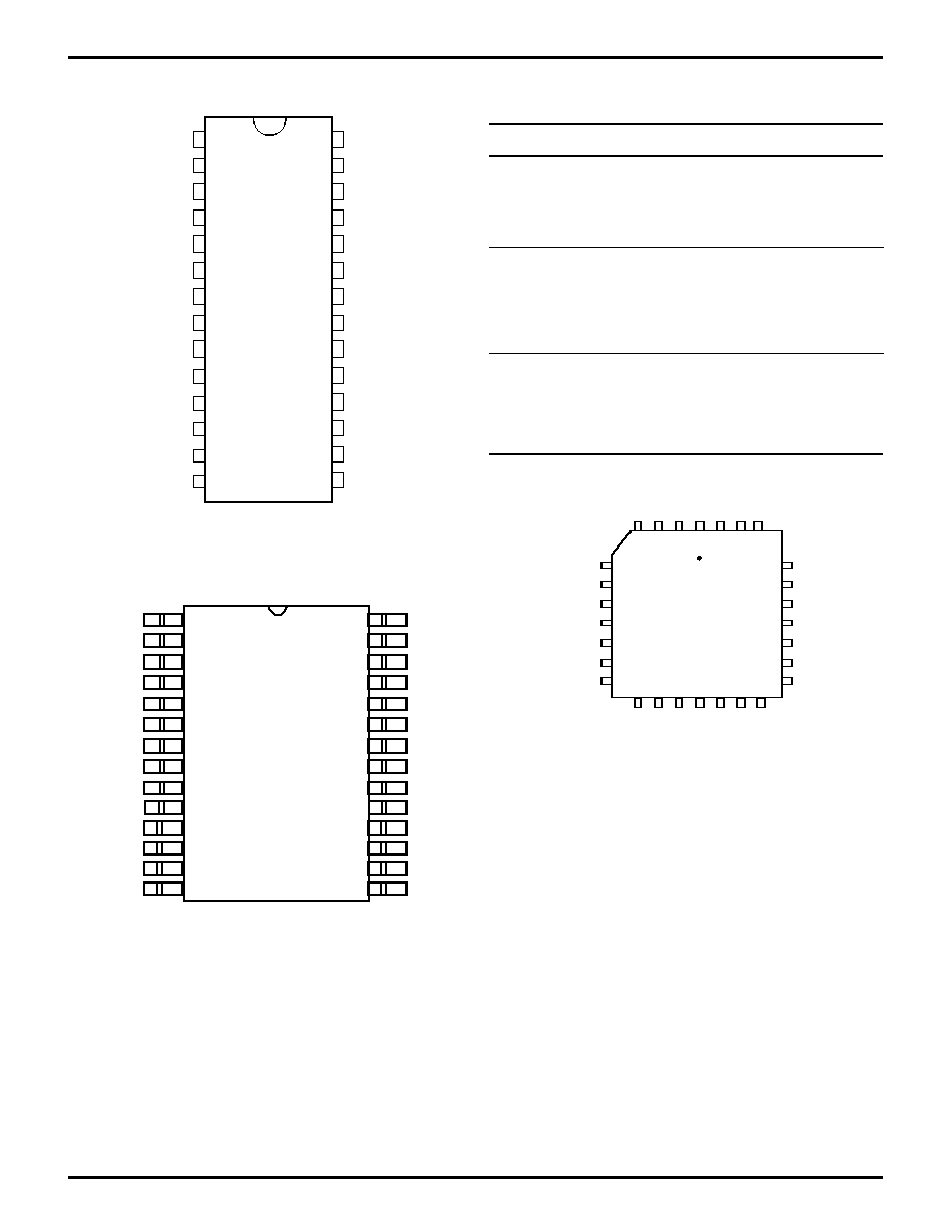
25
19
5
11
18
12
26
4
Z86C30
Z86C31
Z86C32
1
XXX
XXX
XXX
XXX
XXX
XXX
XXX
XXX
XXX
XXX
XXX
XXX
XXX
XXX
P21
P20
P03
VSS
P02
P01
P00
P05
P06
P07
VDD
XT2
XT1
P31
P32
P33
P34
P35
P37
P36
P30
P04
P26
P25
P24
P23
P22
P27
PIN DESCRIPTION
28-Pin DIP/SOIC/PLCC Pin Identification
Pin #
Symbol
Function
Direction
1-3
P27-25
Port 2, Pins 5,6,7
In/Output
4-7
P07-04
Port 0, Pins 4,5,6,7
In/Output
8
V
CC
Power Supply
9
XTAL2
Crystal Oscillator
Output
10
XTAL1
Crystal Oscillator
Input
11-13 P33-31
Port 3, Pins 1,2,3
Fixed Input
14-15
P35-4
Port 3, Pins 4,5
Fixed Output
16
P37
Port 3, Pin 7
Fixed Output
17
P36
Port 3, Pin 6
Fixed Output
18
P30
Port 3, Pin 0
Fixed Input
19-21 P02-00
Port 0, Pins 0,1,2
In/Output
22
GND
Ground, V
SS
23
P03
Port 0, Pin 3
In/Output
24-28 P24-20
Port 2, Pins 0,1,2,3,4 In/Output
P25
P26
P27
P04
P05
P06
P07
VDD
XTAL2
Z86C30
Z86C31
Z86C32
P24
P23
P22
P21
P20
P03
VSS
P02
P01
1
2
3
4
5
6
7
8
9
18
17
16
15
14
13
12
11
10
19
20
XTAL1
P00
21
22
23
24
25
26
27
28
P31
P32
P33
P34
P30
P36
P37
P35
28-Pin SOIC Configuration
28-Pin DIP Configuration
28-Pin PLCC Configuration
1
2
9
3
4
5
6
7
8
28
27
26
25
24
23
22
21
20
P24
P23
P01
P22
P21
P20
P03
GND
P02
P25
P26
XTAL2
P27
P04
P05
P06
P07
VCC
Z86C30
Z86C31
Z86C32
19
18
17
16
15
14
10
11
12
13
XTAL1
P31
P32
P33
P34
P00
P30
P36
P37
P35
4
CP96DZ82900
Z86C30/C31/C32/C40
CP96DZ82900
Z
ILOG
PIN DESCRIPTION
(Continued)
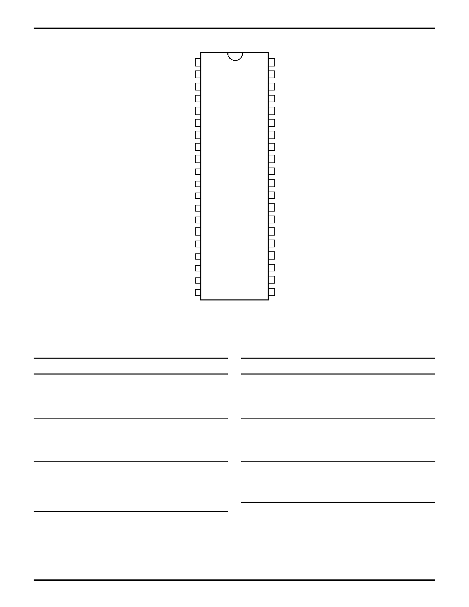
1
2
9
3
4
5
6
7
8
40
39
38
37
36
35
34
33
32
/DS
P24
P12
P23
P22
P21
P20
P03
P13
R//W
XTAL2
P27
P04
P05
P06
P14
31
30
29
28
27
14
10
11
12
13
XTAL1
VCC
P16
P17
P25
GND
P02
P11
P10
P01
Z86C40
15
26
25
24
23
22
21
20
16
17
18
19
P15
P07
P26
P31
P34
/AS
P33
P32
P36
P00
P30
P37
P35
/RESET
40-Pin DIP Assignments
Pin #
Symbol
Function
Direction
1
R//W
Read/Write
Output
2-4
P25-27
Port 2, Pins 5,6,7
In/Output
5-7
P04-06
Port 0, Pins 4,5,6
In/Output
8-9
P14-15
Port 1, Pins 4,5
In/Output
10
P07
Port 0, Pin 7
In/Output
11
V
CC
Power Supply
12-13 P16-17
Port 1, Pins 6,7
In/Output
14
XTAL2
Crystal, Oscillator Clock Output
15
XTAL1
Crystal, Oscillator Clock Input
16-18 P31-33
Port 3, Pins 1,2,3
Input
19
P34
Port 3, Pin 4
Output
20
/AS
Address Strobe
Output
21
/RESET
Reset
Input
40-Pin Dual-In-Line Package Pin Identification
Pin #
Symbol
Function
Direction
22
P35
Port 3, Pin 5
Output
23
P37
Port 3, Pin 7
Output
24
P36
Port 3, Pin 6
Output
25
P30
Port 3, Pin 0
Input
26-27 P00-01
Port 0, Pin 0,1
In/Output
28-29 P10-11
Port 1, Pin 0,1
In/Output
30
P02
Port 0, Pin 2
In/Output
31
GND
Ground, GND
32-33 P12-13
Port 1, Pin 2,3
In/Output
34
P03
Port 0, Pin 3
In/Output
35-39 P20-24
Port 2, Pin 0,1,2,3,4
In/Output
40
/DS
Data Strobe
Output
CP96DZ82900
5
Z86C30/C31/C32/C40
CP96DZ82900
Z
ILOG
PIN DESCRIPTION
(Continued)
P20
P03
P13
P12
GND
GND
P02
P1
1
P10
P01
P00
P05
P06
P14
P15
P07
VCC
VCC
P16
P17
P30
P36
P37
P35
/RESET
R//RL
/AS
P34
P33
P32
P31
P21
P22
P23
P24
/DS
N/C
R//W
P25
P26
P27
P04
7
8
9
10
11
12
13
14
15
16
17
38
37
36
35
34
33
32
31
30
29
39
Z86C40
6
5
4
3
2
1
44 43 42 41 40
18 19 20 21 22 23 24 25 26 27 28
XT
AL1
XT
AL2
44-Pin PLCC Pin Assignments
Pin #
Symbol
Function
Direction
28
XTAL1
Crystal, Oscillator Clock Input
29-31 P31-33
Port 3, Pins 1,2,3
Input
32
P34
Port 3, Pin 4
Output
33
/AS
Address Strobe
Output
34
R//RL
ROM/ROMless Control
Input
35
/RESET
Reset
Input
36
P35
Port 3, Pin 5
Output
37
P37
Port 3, Pin 7
Output
38
P36
Port 3, Pin 6
Output
39
P30
Port 3, Pin 0
Input
40-41 P00-01
Port 0, Pins 0,1
In/Output
42-43 P10-11
Port 1, Pins 0,1
In/Output
44
P02
Port 0, Pin 2
In/Output
Pin #
Symbol
Function
Direction
1-2
GND
Ground, GND
3-4
P12-13
Port 1, Pins 2,3
In/Output
5
P03
Port 0, Pin 3
In/Output
6-10
P20-24
Port 2, Pins 0,1,2,3,4
In/Output
11
/DS
Data Strobe
Output
12
N/C
Not Connected
13
R//W
Read/Write
Output
14-16 P25-27
Port 2, Pins 5,6,7
In/Output
17-19 P04-06
Port 0, Pins 4,5,6
In/Output
20-21 P14-15
Port 1, Pins 4,5
In/Output
22
P07
Port 0, Pin 7
In/Output
23-24 V
CC
Power Supply
25-26 P16-17
Port 1, Pins 6,7
In/Output
27
XTAL2
Crystal, Oscillator Clock Output
44-Pin PLCC Pin Identification
6
CP96DZ82900
Z86C30/C31/C32/C40
CP96DZ82900
Z
ILOG
PIN DESCRIPTION
(Continued)
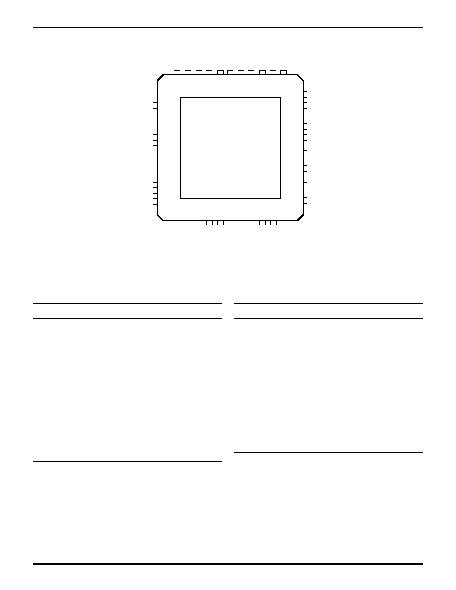
Pin #
Symbol
Function
Direction
1-2
P05-06
Port 0, Pins 5,6
In/Output
3-4
P14-15
Port 1, Pins 4,5
In/Output
5
P07
Port 0, Pin 7
In/Output
6-7
V
CC
Power Supply
8-9
P16-17
Port 1 Pins 6,7
In/Output
10
XTAL2
Crystal, Oscillator Clock Output
11
XTAL1
Crystal, Oscillator Clock Input
12-14 P31-33
Port 3, Pins 1,2,3
Input
15
P34
Port 3, Pin 4
Output
16
/AS
Address Strobe
Output
17
R//RL
ROM/ROMless Control
Input
18
/RESET
Reset
Input
19
P35
Port 3, Pin 5
Output
20
P37
Port 3, Pin 7
Output
Pin #
Symbol
Function
Direction
21
P36
Port 3, Pin 6
Output
22
P30
Port 3, Pin 0
Input
23-24 P00-01
Port 0, Pins 0,1
In/Output
25-26 P10-11
Port 1, Pins 0,1
In/Output
27
P02
Port 0, Pin 2
In/Output
28-29 GND
Ground, GND
30-31 P12-13
Port 1, Pins 2,3
In/Output
32
P03
Port 0, Pin 3
In/Output
33-37 P20-24
Port 2, Pins 0,1,2,3,4
In/Output
38
/DS
Data Strobe
Output
39
N/C
Not Connected
40
R//W
Read/Write
Output
41-43 P25-27
Port 2, Pins 5,6,7
In/Output
44
P04
Port 0, Pin 4
In/Output
44-Pin QFP Pin Assignments
44-Pin QFP Pin Identification
34
35
36
37
38
39
40
41
42
43
44
21
20
19
18
17
16
15
14
13
12
22
33 32 31 30 29 28 27 26 25 24 23
1
2
3
4
5
6
7
8
9
10 11
Z86C40
P20
P03
P13
P12
GND
GND
P02
P1
1
P10
P01
P00
P21
P22
P23
P24
/DS
N/C
R//W
P25
P26
P27
P04
P30
P36
P37
P35
/RESET
R//RL
/AS
P34
P33
P32
P31
P05
P06
P14
P15
P07
VCC
VCC
P16
P17
XT
AL1
XT
AL2
CP96DZ82900
7
Z86C30/C31/C32/C40
CP96DZ82900
Z
ILOG
ABSOLUTE MAXIMUM RATINGS
Parameter
Min
Max
Units
Ambient Temperature under Bias
≠40
+105
C
Storage Temperature
≠65
+150
C
Voltage on any Pin with Respect to V
SS
[Note 1]
≠0.6
+7
V
Voltage on V
DD
Pin with Respect to V
SS
≠0.3
+7
V
Voltage on XTAL1 and /RESET Pins with Respect to V
SS
[Note 2]
≠0.6
V
DD
+1
V
Total Power Dissipation
1.21
W
Maximum Allowable Current out of V
SS
220
mA
Maximum Allowable Current into V
DD
180
mA
Maximum Allowable Current into an Input Pin [Note 3]
≠600
+600
µ
A
Maximum Allowable Current into an Open-Drain Pin [Note 4]
≠600
+600
µ
A
Maximum Allowable Output Current Sinked by Any I/O Pin
25
mA
Maximum Allowable Output Current Sourced by Any I/O Pin
25
mA
STANDARD TEST CONDITIONS
The characteristics listed below apply for standard test
conditions as noted. All voltages are referenced to Ground.
Positive current flows into the referenced pin (Test Load).
CAPACITANCE
T
A
= 25
∞
C, V
CC
= GND = 0V, f = 1.0 MHz; unmeasured pins returned to GND.
Parameter
Min
Max
Input capacitance
0
12 pF
Output capacitance
0
12 pF
I/O capacitance
0
12 pF
Notes:
[1] This applies to all pins except XTAL pins and where otherwise noted.
[2] There is no input protection diode from pin to V
DD
.
[3] This excludes XTAL pins.
[4] Device pin is not at an output Low state.
Total power dissipation should not exceed 1.21 W for the
package. Power dissipation is calculated as follows:
Total Power Dissipation = V
DD
x [ I
DD
≠ (sum of I
OH
) ]
+ sum of [ (V
DD
≠ V
OH
) x I
OH
]
+ sum of (V
0L
x I
0L
)
Notice:
Stresses greater than those listed under Absolute Maxi-
mum Ratings may cause permanent damage to the de-
vice. This is a stress rating only; functional operation of the
device at any condition above those indicated in the
operational sections of these specifications is not implied.
Exposure to absolute maximum rating conditions for an
extended period may affect device reliability.
From Output
Under Test
150 pF
Test Load Diagram

8
CP96DZ82900
Z86C30/C31/C32/C40
CP96DZ82900
Z
ILOG
DC ELECTRICAL CHARACTERISTICS
T
A
= 0
∞
C
Typical [1]
V
CC
to +70
∞
C
@
Sym
Parameter
Note [3]
Min
Max
25
∞
C
Units
Conditions
Notes
V
CH
Clock Input High Voltage 3.0V
0.7 V
CC
V
CC
+0.3
1.3
V
Driven by External Clock Generator
5.5V
0.7 V
CC
V
CC
+0.3
2.5
V
Driven by External Clock Generator
V
CL
Clock Input Low Voltage
3.0V
GND-0.3
0.2 V
CC
0.7
V
Driven by External Clock Generator
5.5V
GND-0.3
0.2 V
CC
1.5
V
Driven by External Clock Generator
V
IH
Input High Voltage
3.0V
0.7 V
CC
V
CC
+0.3
1.3
V
5.5V
0.7 V
CC
V
CC
+0.3
2.5
V
V
IL
Input Low Voltage
3.0V
GND-0.3
0.2 V
CC
0.7
V
5.5V
GND-0.3
0.2 V
CC
1.5
V
V
OH
Output High Voltge
3.0V
V
CC
≠0.4
3.1
V
I
OH
= ≠ 0.5 mA
Low EMI Mode
5.5V
V
CC
≠0.4
4.8
V
I
OH
= ≠ 0.5 mA
V
OH1
Output High Voltage
3.0V
V
CC
≠0.4
3.1
V
I
OH
= ≠ 2.0 mA
[8]
5.5V
V
CC
≠0.4
4.8
V
I
OH
= ≠ 2.0 mA
[8]
V
OL
Output Low Voltage
3.0V
0.6
0.3
V
I
OL
= 1.0 mA
Low EMI Mode
5.5V
0.4
0.2
V
I
OL
= 1.0 mA
V
OL1
Output Low Voltage
3.0V
0.6
0.2
V
I
OL
= + 4.0 mA
[8]
5.0V
0.4
0.1
V
I
OL
= + 4.0 mA
[8]
V
OL2
Output Low Voltage
3.0V
1.2
0.5
V
I
OL
= + 6 mA
[8]
5.5V
1.2
0.5
V
I
OL
= + 12 mA
[8]
V
RH
Reset Input High Voltage
3.0V
.8 V
CC
V
CC
1.5
V
[7]
5.5V
.8 V
CC
V
CC
2.1
V
[7]
V
RL
Reset Input Low Voltage
3.0V
GND≠0.3
0.2 V
CC
1.1
[7]
5.5V
GND≠0.3
0.2 V
CC
1.7
[7]
V
OLR
Reset Outut Low Voltage
3.0V
0.6
0.3
V
I
OL
= +1.0 mA
[7]
5.5V
0.6
0.2
V
I
OL
= +1.0 mA
[7]
V
OFFSET
Comparator Input Offset
3.0V
25
10
mV
Voltage
5.5V
25
10
mV
V
ICR
Input Common Mode
3.0V
GND-0.3 V
CC
≠1.0V
V
[10]
Voltage Range
5.5V
GND-0.3 V
CC
≠1.0V
V
[10]
I
IL
Input Leakage
3.0V
≠1
2
0.064
µ
A
V
IN
= OV, V
CC
5.5V
≠1
2
0.064
µ
A
V
IN
= OV, V
CC
I
OL
Output Leakage
3.0V
≠1
2
0.114
µ
A
V
IN
= OV, V
CC
5.5V
≠1
2
0.114
µ
A
V
IN
= OV, V
CC
I
IR
Reset Input Current
3.0V
≠20
≠130
≠62
µ
A
5.5V
≠20
≠180
≠112
µ
A
I
CC
Supply Current
3.0V
20
7
mA
@ 16 MHz
[4,5]
5.5V
25
20
mA
@ 16 MHz
[4,5]
3.0V
15
5
mA
@ 12 MHz
[4,5]
5.5V
20
15
mA
@ 12 MHz
[4,5]

CP96DZ82900
9
Z86C30/C31/C32/C40
CP96DZ82900
Z
ILOG
DC ELECTRICAL CHARACTERISTICS
(Continued)
T
A
= 0
∞
C
Typical [1]
V
CC
to +70
∞
C
@
Sym
Parameter
Note [3]
Min
Max
25
∞
C
Units
Conditions
Notes
I
CC1
Standby Current
3.0V
4.5
2.0
mA
V
IN
= 0V, V
CC
@ 16 MHz
[4,5]
(Halt Mode)
5.5V
8
3.7
mA
V
IN
= 0V, V
CC
@ 16 MHz
[4,5]
3.0V
4
1.5
mA
V
IN
= 0V, V
CC
@ 12 MHz
[4,5]
5.5V
6
3.2
mA
V
IN
= 0V, V
CC
@ 12 MHz
[4,5]
3.0V
3.4
1.5
mA
Clock Divide by 16 @ 16 MHz
[4,5]
5.5V
7.0
2.9
mA
Clock Divide by 16 @ 16 MHz
[4,5]
3.0V
3
1.2
mA
Clock Divide by 16 @ 12 MHz
[4,5]
5.5V
5
2.5
mA
Clock Divide by 16 @ 12 MHz
[4,5]
I
CC2
Standby Current
3.0V
8
2
µ
A
V
IN
= OV, V
CC
[6,11]
(Stop Mode)
WDT is not Running
5.5V
10
4
µ
A
V
IN
= OV, V
CC
[6,11]
WDT is not Running
3.0V
500
310
µ
A
V
IN
= OV, V
CC
[6,11]
WDT is Running
5.5V
800
600
µ
A
V
IN
= OV, V
CC
[6,11]
WDT is Running
I
ALL
Auto Latch
3.0V
0.7
8
2.4
µ
A
OV < V
IN
< V
CC
[9]
Low Current
5.5V
1.4
15
4.7
µ
A
OV < V
IN
< V
CC
[9]
I
ALH
Auto Latch
3.0V
≠0.6
≠5
≠1.8
µ
A
OV < V
IN
< V
CC
[9]
High Current
5.5V
≠1
≠8
≠3.8
µ
A
OV < V
IN
< V
CC
[9]
T
POR
Power On Reset
3.0V
3
24
10
mS
5.5V
2.0
13
4
mS
V
LV
Low Voltage Protection
2.05
2.95
2.6
V
6 MHz max INT CLK Freq.
[7]
Note:
[1] Typicals are at V
CC
= 5.0V and 3.3V.
[2] GND = 0V.
[3] The V
CC
voltage spec. of 3.0V guarantees 3.3V
±
0.3V and the V
DD
voltage spec. of 5.5V guarantees 5.0V
±
0.5V.
[4] All outputs unloaded, I/O pins floating, inputs at rail.
[5] CL1= CL2 = 10 pF.
[6] Same as note [4] except inputs at V
CC
.
[7] Z86C40 only.
[8] STD Mode (not Low-EMI Mode).
[9] Auto Latch (mask option) selected.
[10] For analog comparator inputs when analog comparators are enabled.
[11] Clock must be forced Low, when XTAL1 is clock driven and XTAL2 is floating.

10
CP96DZ82900
Z86C30/C31/C32/C40
CP96DZ82900
Z
ILOG
DC ELECTRICAL CHARACTERISTICS
T
A
=≠40
∞
C
Typical [1]
V
CC
to 105
∞
C
@
Sym Parameter
Note [3]
Min
Max
25
∞
C
Units
Conditions
Notes
V
CH
Clock Input High Voltage 3.0V
0.7 V
CC
V
CC
+0.3
1.3
V
Driven by External Clock Generator
5.5V
0.7 V
CC
V
CC
+0.3
2.5
V
Driven by External Clock Generator
V
CL
Clock Input Low Voltage
3.0V
GND-0.3
0.2 V
CC
0.7
V
Driven by External Clock Generator
5.5V
GND-0.3
0.2 V
CC
1.5
V
Driven by External Clock Generator
V
IH
Input High Voltage
3.0V
0.7 V
CC
V
CC
+0.3
1.3
V
5.5V
0.7 V
CC
V
CC
+0.3
2.5
V
V
IL
Input Low Voltage
3.0V
GND-0.3
0.2 V
CC
0.7
V
5.5V
GND-0.3
0.2 V
CC
1.5
V
V
OH
Output High Voltage
3.0V
V
CC
≠0.4
3.1
V
I
OH
= ≠ 0.5 mA
Low EMI Mode
5.5V
V
CC
≠0.4
4.8
V
I
OH
= ≠ 0.5 mA
V
OH1
Output High Voltage
3.0V
V
CC
≠0.4
3.1
V
I
OH
= ≠ 2.0 mA
[8]
5.5V
V
CC
≠0.4
4.8
V
I
OH
= ≠ 2.0 mA
[8]
V
OL
Output Low Voltage
3.0V
0.6
0.3
V
I
OL
= 1.0 mA
Low EMI Mode
5.5V
0.4
0.2
V
I
OL
= 1.0 mA
V
OL1
Output Low Voltage
3.0V
0.6
0.2
V
I
OL
= + 4.0 mA
[8]
5.0V
0.4
0.1
V
I
OL
= + 4.0 mA
[8]
V
OL2
Output Low Voltage
3.0V
1.2
0.5
V
I
OL
= + 6 mA
[8]
5.5V
1.2
0.5
V
I
OL
= + 12 mA
[8]
V
RH
Reset Input High Voltage
3.0V
.8 V
CC
V
CC
1.5
V
[7]
5.5V
.8 V
CC
V
CC
2.1
V
[7]
V
RL
Reset Input Low Voltage
3.0V
GND≠0.3
0.2 V
CC
1.1
[7]
5.5V
GND≠0.3
0.2 V
CC
1.7
[7]
V
OLR
Reset Output Low Voltage 3.0V
0.6
0.4
V
I
OL
= + 1.0 mA
[7]
5.5V
0.6
0.3
V
I
OL
= + 1.0 mA
[7]
V
OFFSET
Comparator Input Offset
3.0V
25
10
mV
Voltage
5.5V
25
10
mV
V
ICR
Input Common Mode
3.0V
GND≠0.3
V
CC
≠1.5V
V
[10]
Voltage Range
5.5V
GND≠0.3
V
CC
≠1.5V
V
[10]
I
IL
Input Leakage
3.0V
≠1
2
<1
µ
A
V
IN
= OV, V
CC
5.5V
≠1
2
<1
µ
A
V
IN
= OV, V
CC
I
OL
Output Leakage
3.0V
≠1
2
<1
µ
A
V
IN
= OV, V
CC
5.5V
≠1
2
<1
µ
A
V
IN
= OV, V
CC
I
IR
Reset Input Current
3.0V
≠18
≠130
≠62
µ
A
5.5V
≠18
≠180
≠112
µ
A
I
CC
Supply Current
3.0V
20
7
mA
@ 16 MHz
[4,5]
5.5V
25
20
mA
@ 16 MHz
[4,5]
3.0V
15
5
mA
@ 12 MHz
[4,5]
5.5V
20
15
mA
@ 12 MHz
[4,5]

CP96DZ82900
11
Z86C30/C31/C32/C40
CP96DZ82900
Z
ILOG
DC ELECTRICAL CHARACTERISTICS
(Continued)
T
A
= ≠40
∞
C
Typical [1]
V
CC
to 105
∞
C
@
Sym Parameter
Note [3]
Min
Max
25
∞
C
Units
Conditions
Notes
I
CC1
Standby Current
3.0V
4.5
2.0
mA
V
IN
= 0V, V
CC
@ 16 MHz
[4,5]
(Halt Mode)
5.5V
8
3.7
mA
V
IN
= 0V, V
CC
@ 16 MHz
[4,5]
3.0V
4
1.5
mA
V
IN
= 0V, V
CC
@ 12 MHz
[4,5]
5.5V
6
3.2
mA
V
IN
= 0V, V
CC
@ 12 MHz
[4,5]
3.0V
3.4
1.5
mA
Clock Divide by 16 @ 16 MHz
[4,5]
5.5V
7.0
2.9
mA
Clock Divide by 16 @ 16 MHz
[4,5]
3.0V
3
1.2
mA
Clock Divide by 16 @ 12 MHz
[4,5]
5.5V
5
2.5
mA
Clock Divide by 16 @ 12 MHz
[4,5]
I
CC2
Standby Current
3.0V
8
2
µ
A
V
IN
= OV, V
CC
[6,11]
(Stop Mode)
WDT is not Running
5.5V
10
4
µ
A
V
IN
= OV, V
CC
[6,11]
WDT is not Running
3.0V
600
310
µ
A
V
IN
= OV, V
CC
[6,11]
WDT is Running
5.5V
1000
600
µ
A
V
IN
= OV, V
CC
[6,11]
WDT is Running
I
ALL
Auto Latch Low Current
3.0V
0.7
10
2.4
µ
A
OV < V
IN
< V
CC
[9]
5.5V
1.4
20
4.7
µ
A
OV < V
IN
< V
CC
[9]
I
ALH
Auto Latch High Current
3.0V
≠0.6
≠7
≠1.8
µ
A
OV < V
IN
< V
CC
[9]
5.5V
≠1.0
≠10
≠3.8
µ
A
OV < V
IN
< V
CC
[9]
T
POR
Power On Reset
3.0V
3.0
25
7
mS
5.5V
2.0
14
4
mS
V
LV
Low Voltage Protection
1.8
3.3
2.6
V
4 MHz max INT CLK Freq.
Note:
[1] Typicals are at V
CC
= 5.0V and 3.3V.
[2] GND=0V.
[3] The V
CC
voltage spec. of 3.0V guarantees 3.3V
±
0.3V and the V
DD
voltage spec. of 5.5V guarantees 5.0V
±
0.5V.
[4] All outputs unloaded, I/O pins floating, inputs at rail.
[5] CL1= CL2 = 100pF.
[6] Same as note [4] except inputs at V
CC
.
[[7] Z86C40 only.
[8] STD Mode (not Low EMI Mode).
[9] Auto Latch (mask option) selected.
[10] For analog comparator inputs when analog comparators are enabled.
[11] Clock must be forced Low, when XTAL1 is clock driven and XTAL2 is floating.
[7] Z86C40 only.
12
CP96DZ82900
Z86C30/C31/C32/C40
CP96DZ82900
Z
ILOG
AC CHARACTERISTICS
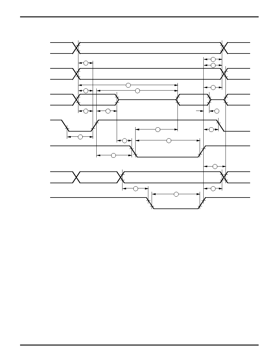
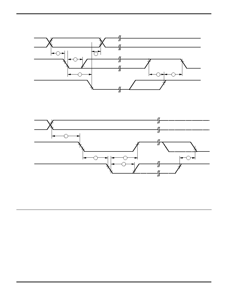
External I/O or Memory Read and Write Timing Diagram (Z86C40 Only)
R//W, /DM
9
12
18
3
16
13
4
5
8
11
6
17
10
15
7
14
2
1
Port 0
Port 1
/AS
/DS
(Read)
Port1
/DS
(Write)
A7 - A0
D7 - D0 IN
D7 - D0 OUT
A7 - A0
19
20
External I/O or Memory Read/Write Timing
(Z86C40 Only)

CP96DZ82900
13
Z86C30/C31/C32/C40
CP96DZ82900
Z
ILOG
AC CHARACTERISTICS
External I/O or Memory Read and Write Timing Table (Z86C40 Only)
(SCLK/TCLK = XTAL/2)
T
A
=≠40
∞
C to 105
∞
C
T
A
= ≠40
∞
C to +105
∞
C
Note [3]
12 MHz
16 MHz
12 MHz
16 MHz
No Symbol Parameter
V
CC
Min Max Min Max
Min Max Min Max Units
Notes
1 TdA(AS)
Address Valid to /AS Rise Delay
3.0
35
25
35
25
ns
[2]
5.5
35
25
35
25
ns
2 TdAS(A)
/AS Rise to Address Float Delay
3.0
45
35
45
35
ns
[2]
5.5
45
35
45
35
ns
3 TdAS(DR)
/AS Rise to Read Data Req'd Valid
3.0
250
180
250
180
ns
[1,2]
5.5
250
180
250
180
ns
4 TwAS
/AS Low Width
3.0
55
40
55
40
ns
[2]
5.5
55
40
55
40
ns
5 TdAS(DS)
Address Float to /DS Fall
3.0
0
0
0
0
ns
5.5
0
0
0
0
ns
6 TwDSR
/DS (Read) Low Width
3.0
200
135
200
135
ns
[1,2]
5.5
200
135
200
135
ns
7 TwDSW
/DS (Write) Low Width
3.0
110
80
110
80
ns
[1,2]
5.5
110
80
110
80
ns
8 TdDSR(DR) /DS Fall to Read Data Req'd Valid
3.0
150
75
150
75
ns
[1,2]
5.5
150
75
150
75
ns
9 ThDR(DS)
Read Data to /DS Rise Hold Time
3.00
0
0
0
0
ns
[2]
5.5
0
0
0
0
ns
10 TdDS(A)
/DS Rise to Address Active Delay
3.0
45
50
45
50
ns
[2]
5.5
55
50
55
50
ns
11 TdDS(AS)
/DS Rise to /AS Fall Delay
3.0
30
35
30
35
ns
[2]
5.5
45
35
45
55
ns
12 TdR/W(AS) R//W Valid to /AS Rise Delay
3.0
45
25
45
25
ns
[2]
5.5
45
25
45
25
ns
13 TdDS(R/W) /DS Rise to R//W Not Valid
3.0
45
35
45
35
ns
[2]
5.5
45
35
45
35
ns
14 TdDW(DSW) Write Data Valid to /DS Fall (Write) Delay 3.0
55
25
55
25
ns
[2]
5.5
55
25
55
25
ns
15 TdDS(DW) /DS Rise to Write Data Not Valid Delay
3.0
45
35
45
35
ns
[2]
5.5
45
35
45
35
ns
16 TdA(DR)
Address Valid to Read Data Req'd Valid
3.0
310
230
310
230
ns
[1,2]
5.5
310
230
310
230
ns
17 TdAS(DS)
/AS Rise to /DS Fall Delay
3.0
65
45
65
45
ns
[2]
5.5
65
45
65
45
ns
18 TdDM(AS) /DM Valid to /AS Fall Delay
3.0
35
30
35
30
ns
[2]
5.5
35
30
35
30
ns
19 TdDS(DM) /DS Rise to DM Valid Delay
3.0
45
35
45
35
ns
5.5
45
35
45
35
ns
20 ThDS(AS)
/DS Valid to Address Valid Hold Time
3.0
45
35
45
35
ns
5.5
45
35
45
35
ns
Notes:
[1] When using extended memory timing add 2 TpC.
[2] Timing numbers given are for minimum TpC.
[3] The V
CC
voltage specification of 3.0V guarantees 3.3V
±
0.3V, and the
V
DD
voltage specification of 5.5V guarantees 5.0V
±
0.5V.
Standard Test Load
All timing references use 0.7 V
CC
for a logic 1 and 0.2 V
CC
for a logic 0.
For Standard Mode (not Low-EMI Mode for outputs) with SMR D1 = 0,
D0 = 0.
14
CP96DZ82900
Z86C30/C31/C32/C40
CP96DZ82900
Z
ILOG
AC ELECTRICAL CHARACTERISTICS
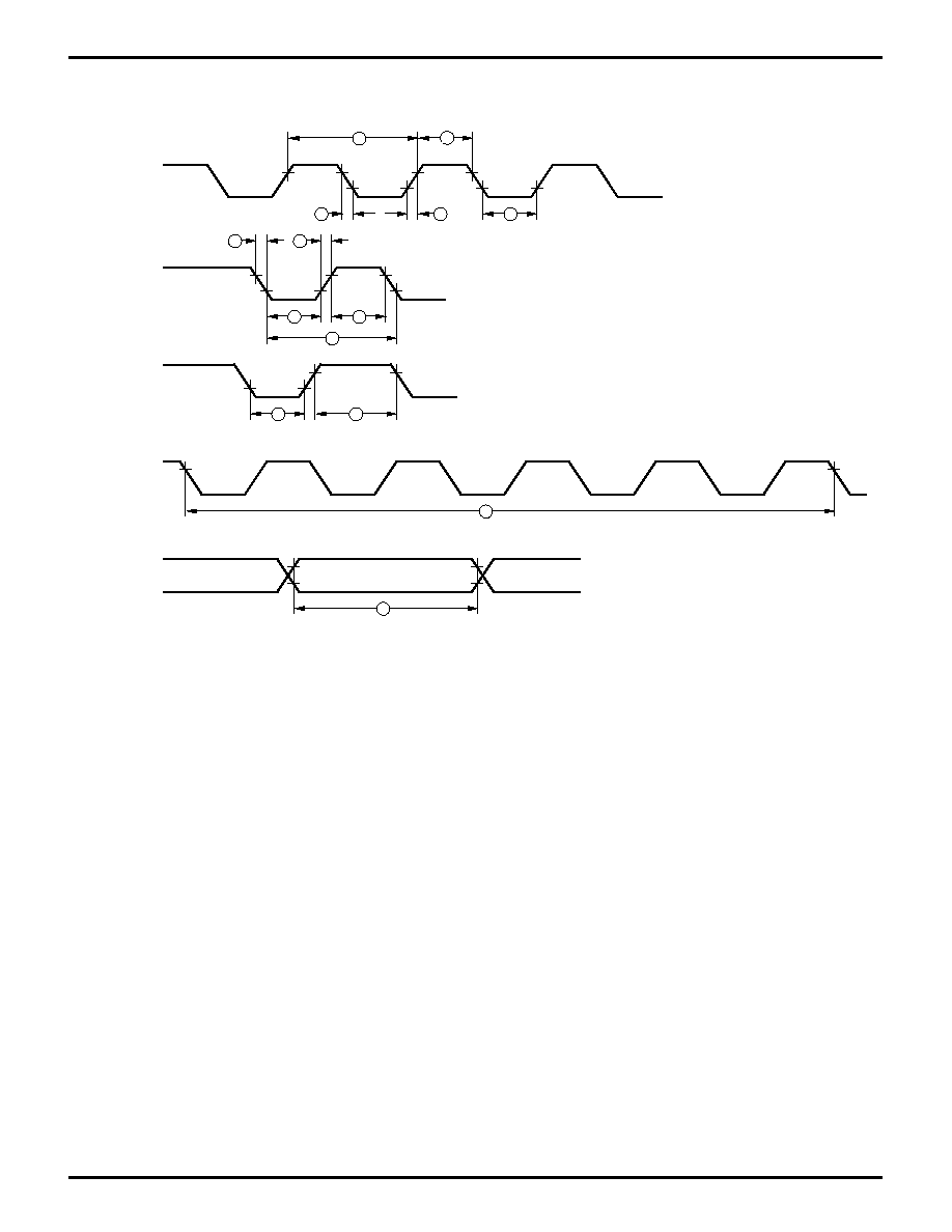
Additional Timing Diagram
Additional Timing
Clock
1
3
4
8
2
2
3
TIN
IRQN
6
5
7
7
11
Clock
Setup
10
9
Stop
Mode
Recovery
Source

CP96DZ82900
15
Z86C30/C31/C32/C40
CP96DZ82900
Z
ILOG
AC ELECTRICAL CHARACTERISTICS
Additional Timing Table (Divide-By-One Mode)
T
A
= 0
∞
C to +70
∞
C
T
A
= 40
∞
C to +105
∞
C
V
CC
4 MHz
4 MHz
No Symbol
Parameter
Note [6]
Min
Max
Min
Max
Units
Notes
1
TpC
Input Clock Period
3.0V
250
DC
250
DC
ns
[1,7,8]
5.5V
250
DC
250
DC
ns
[1,7,8]
2
TrC,TfC
Clock Input Rise & Fall Times
3.0V
25
25
ns
[1,7,8]
5.5V
25
25
ns
[1,7,8]
3
TwC
Input Clock Width
3.0V
100
100
ns
[1,7,8]
5.5V
100
100
ns
[1,7,8]
4
TwTinL
Timer Input Low Width
3.0V
100
100
ns
[1,7,8]
5.5V
70
70
ns
[1,7,8]
5
TwTinH
Timer Input High Width
3.0V
5TpC
5TpC
[1,7,8]
5.5V
5TpC
5TpC
[1,7,8]
6
TpTin
Timer Input Period
3.0V
8TpC
8TpC
[1,7,8]
5.5V
8TpC
8TpC
[1,7,8]
7
TrTin,
Timer Input Rise & Fall Timer
3.0V
100
100
ns
[1,7,8]
TfTin
5.5V
100
100
ns
[1,7,8]
8A
TwIL
Int. Request Low Time
3.0V
100
100
ns
[1,2,7,8]
5.5V
70
70
ns
[1,2,7,8]
8B
TwIL
Int. Request Low Time
3.0V
5TpC
5TpC
[1,3,7,8]
5.5V
5TpC
5TpC
[1,3,7,8]
9
TwIH
Int. Request Input High Time
3.0V
5TpC
5TpC
[1,2,7,8]
5.5V
5TpC
5TpC
[1,2,7,8]
10
Twsm
STOP Mode Recovery Width Spec 3.0V
12
12
ns
[4,8]
5.5V
12
12
ns
[4,8]
11
Tost
Oscillator Start-up Time
3.0V
5TpC
5TpC
[4,8,9]
5.5V
5TpC
5TpC
[4,8,9]
Notes:
[1] Timing Reference uses 0.7 V
CC
for a logic 1 and 0.2 V
CC
for a logic 0.
[2] Interrupt request via Port 3 (P31-P33).
[3] Interrupt request via Port 3 (P30).
[4] SMR-D5 = 1, POR STOP Mode Delay is on.
[5] Reg. WDTMR.
[6] The V
CC
voltage specification of 3.0V guarantees 3.3V
±
0.3V, and
the V
DD
voltage specification of 5.5V guarantees 5.0V
±
0.5V.
[7] SMR D1 = 0.
[8] Maximum frequency for internal system clock is 4 MHz when
using XTAL divide-by-one mode.
[9] For RC and LC oscillator, and for oscillator driven by clock driver.

16
CP96DZ82900
Z86C30/C31/C32/C40
CP96DZ82900
Z
ILOG
AC ELECTRICAL CHARACTERISTICS
Additional Timing Table
T
A
= ≠40
∞
C to +105
∞
C
T
A
= 0
∞
C to +70
∞
C
V
CC
16 MHz
12 MHz
No Symbol
Parameter
Note [6]
Min
Max
Min
Max
Units
Notes
1
TpC
Input Clock Period
3.0V
62.5
DC
83
DC
ns
[1,7,8]
5.5V
62.5
DC
83
DC
ns
[1,7,8]
2
TrC,TfC
Clock Input Rise & Fall Times
3.0V
15
15
ns
[1,7,8]
5.5V
15
15
ns
[1,7,8]
3
TwC
Input Clock Width
3.0V
31
26
ns
[1,7,8]
5.5V
31
26
ns
[1,7,8]
4
TwTinL
Timer Input Low Width
3.0V
100
100
ns
[1,7,8]
5.5V
70
70
ns
[1,7,8]
5
TwTinH
Timer Input High Width
3.0V
5TpC
5TpC
[1,7,8]
5.5V
5TpC
5TpC
[1,7,8]
6
TpTin
Timer Input Period
3.0V
8TpC
8TpC
[1,7,8]
5.5V
8TpC
8TpC
[1,7,8]
7
TrTin,
Timer Input Rise & Fall Timer
3.0V
100
100
ns
[1,7,8]
TfTin
5.5V
100
100
ns
[1,7,8]
8A TwIL
Int. Request Low Time
3.0V
100
100
ns
[1,2,7,8]
5.5V
70
70
ns
[1,2,7,8]
8B TwIL
Int. Request Low Time
3.0V
5TpC
5TpC
[1,3,7,8]
5.5V
5TpC
5TpC
[1,3,7,8]
9
TwIH
Int. Request Input High Time
3.0V
5TpC
5TpC
[1,2,7,8]
5.5V
5TpC
5TpC
[1,2,7,8]
10 Twsm
STOP Mode Recovery Width Spec 3.0V
12
12
ns
[4,8]
5.5V
12
12
ns
[4,8]
11 Tost
Oscillator Start-up Time
3.0V
5TpC
5TpC
[4,8]
5.5V
5TpC
5TpC
[4,8]
12 Twdt
Watch-Dog Timer Delay Time
3.0V
10
10
ms
D0 = 0 [5,11]
Before Refresh
5.5V
5
5.0
ms
D1 = 0 [5,11]
3.0V
20
20
ms
D0 = 1 [5,11]
5.5V
10
10
ms
D1 = 0 [5,11]
3.0V
40
40
ms
D0 = 0 [5,11]
5.5V
20
20
ms
D1 = 1 [5,11]
3.0V
160
160
ms
D0 = 1 [5,11]
5.5V
80
80
ms
D1 = 1 [5,11]
Notes:
[1] Timing Reference uses 0.7 V
CC
for a logic 1 and 0.2 V
CC
for a logic 0.
[2] Interrupt request via Port 3 (P31-P33).
[3] Interrupt request via Port 3 (P30).
[4] SMR-D5 = 1, POR STOP Mode Delay is on.
[5] Reg. WDTMR.
[6] The V
CC
voltage spec. of 3.0V guarantees 3.3V
±
0.3V and the V
DD
voltage spec. of 5.5V guarantees 5.0V
±
0.5V.
[7] SMR D1 = 0.
[8] Maximum frequency for internal system clock is 4 MHz when using XTAL divide-by-one mode.
[9] For RC and LC oscillator, and for oscillator driven by clock driver.
[10] Standard Mode (not Low EMI output ports).
[11] Using internal RC.
CP96DZ82900
17
Z86C30/C31/C32/C40
CP96DZ82900
Z
ILOG
AC ELECTRICAL CHARACTERISTICS
Handshake Timing Diagrams
Input Handshake Timing
Output Handshake Timing
Data Out
/DAV
(Output)
RDY
(Input)
Next Data Out Valid
Delayed RDY
Delayed DAV
Data Out Valid
7
8
9
10
11
Data In
1
2
3
4
5
6
/DAV
(Input)
RDY
(Output)
Next Data In Valid
Delayed RDY
Delayed DAV
Data In Valid
Zilog's products are not authorized for use as critical compo-
nents in life support devices or systems unless a specific written
agreement pertaining to such intended use is executed between
the customer and Zilog prior to use. Life support devices or
systems are those which are intended for surgical implantation
into the body, or which sustains life whose failure to perform,
when properly used in accordance with instructions for use
provided in the labeling, can be reasonably expected to result in
significant injury to the user.
Zilog, Inc. 210 East Hacienda Ave.
Campbell, CA 95008-6600
Telephone (408) 370-8000
Telex 910-338-7621
FAX 408 370-8056
Internet: http://www.zilog.com
© 1997 by Zilog, Inc. All rights reserved. No part of this document
may be copied or reproduced in any form or by any means
without the prior written consent of Zilog, Inc. The information in
this document is subject to change without notice. Devices sold
by Zilog, Inc. are covered by warranty and patent indemnification
provisions appearing in Zilog, Inc. Terms and Conditions of Sale
only. Zilog, Inc. makes no warranty, express, statutory, implied or
by description, regarding the information set forth herein or
regarding the freedom of the described devices from intellectual
property infringement. Zilog, Inc. makes no warranty of mer-
chantability or fitness for any purpose. Zilog, Inc. shall not be
responsible for any errors that may appear in this document.
Zilog, Inc. makes no commitment to update or keep current the
information contained in this document.