1
Z86C61/62/96
Z8
Æ
M
ICROCONTROLLER
P
RODUCT
S
PECIFICATION
Z86C61/62/96
CMOS Z8
Æ
M
ICROCONTROLLER
FEATURES
s
8-Bit CMOS Microcontroller
s
40-Pin DIP, 44-Pin PLCC, 64-Pin DIP, or
68-Pin PLCC Package
s
32 Input/Output Lines (Z86C61 Only)
s
52 Input/Output Lines (Z86C62 and Z86C96)
s
3.0V to 5.5V Operating Range
s
Low Power Consumption: 200 mW (max)
s
Fast Instruction Pointer: 0.75
µ
s @ 16 MHz
s
Two Standby Modes: STOP and HALT
s
Full-Duplex UART
s
All Digital Inputs are TTL Levels
GENERAL DESCRIPTION
The Z86C61/62/96 microcontroller is a member of the Z8
single-chip microcontroller family with 16 Kbytes of ROM
and 256 bytes of RAM. The Z86C96 is ROMless.
The Z86C61 is offered in 40-pin DIP and 44-pin PLCC style
packages, however, the ROMless pin option is available
on the 44-pin version only. The Z86C62/96 is offered in 64-
pin DIP and 68-pin PLCC style packages. A ROMless pin
option enables these MCUs to address both external
memory and preprogrammed ROM, making them well-
suited for high-volume applications or where code flexibil-
ity is required.
With 16 Kbytes of ROM and 256 bytes of general-purpose
RAM, these low-cost, low power consumption CMOS
Z86C61/62/96 MCUs offer fast execution, efficient use of
memory, sophisticated interrupts, input/output bit manipu-
lation capabilities, and easy hardware/software system
expansion.
The Z86C61/62/96 architecture is characterized by Zilog's
8-bit microcontroller core. The device offers a flexible I/O
scheme, an efficient register and address space structure,
multiplexed capabilities between address/data, I/O, and a
number of ancillary features that are useful in many indus-
trial and advanced scientific applications.
For applications which demand powerful I/O capabilities,
the Z86C61 fulfills this with 32 pins dedicated to input and
output. These lines are grouped into four ports with eight
lines each. The Z86C62/96 has 52 pins for input and
output, and these lines are grouped into six, 8-bit ports and
one 4-bit port. Each port is configurable under software
control to provide timing, status signals, serial or parallel
I/O with or without handshake, and an address/data bus
for interfacing external memory.
s
Auto Latches
s
RAM and ROM Protect
s
16 Kbytes of ROM
s
256 Bytes of RAM
s
Two Programmable 8-Bit Counter/Timers,
Each with 6-Bit Programmable Prescaler
s
Six Vectored, Priority Interrupts from Eight
Different Sources
s
Clock Speeds: 16 and 20 MHz
s
On-Chip Oscillator that Accepts a Crystal,
Ceramic Resonator, LC, or External Clock Drive

2
Z86C61/62/96
Z8
Æ
M
ICROCONTROLLER
GENERAL DESCRIPTION
(Continued)
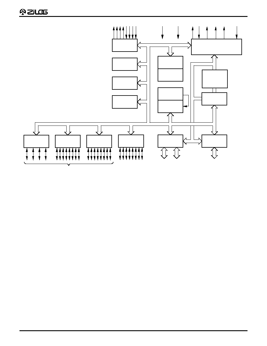
There are three basic address spaces available to support
this configuration: Program Memory, Data Memory, and
236 General-Purpose Registers.
To unburden the program from coping with the real-time
tasks, such as counting/timing and serial data communi-
cation, the Z86C61/62/96 offers two on-chip counter/tim-
ers with a large number of user selectable modes, and an
on-board UART (Figures 1, 2, and 3).
Notes:
All Signals with a preceding front slash, "/", are active Low, e.g.,
B//W (WORD is active Low); /B/W (BYTE is active Low, only).
Power connections follow conventional descriptions below:
Connection
Circuit
Device
Power
V
CC
V
DD
Ground
GND
V
SS
Port 3
UART
Counter/
Timers
(2)
Interrupt
Control
Port 2
I/O
(Bit Programmable)
ALU
FLAGS
Register
Pointer
Register File
256 x 8-Bit
Machine Timing and
Instruction Control
Prg. Memory
16,384
x 8-Bit
Program
Counter
Vcc
GND
XTAL
4
4
Port 0
Output
Input
Address or I/O
(Nibble Programmable)
Port 1
8
Address/Data or I/O
(Byte Programmable)
/AS /DS R//W /RESET
Figure 1. Z86C61 Functional Block Diagram

5
Z86C61/62/96
Z8
Æ
M
ICROCONTROLLER
PIN DESCRIPTION
Table 1. Z86C61 40-Pin DIP Pin Identification
Pin #
Symbol
Function
Direction
1
V
CC
Power Supply
Input
2
XTAL2
Crystal, Oscillator Clock
Output
3
XTAL1
Crystal, Oscillator Clock
Input
4
P37
Port 3, Pin 7
Output
5
P30
Port 3, Pin 0
Input
6
/RESET
Reset
Input
7
R//W
Read/Write
Output
8
/DS
Data Strobe
Output
9
/AS
Address Strobe
Output
10
P35
Port 3, Pin 5
Output
11
GND
Ground
Input
12
P32
Port 3, Pin 2
Input
13-20
P07-P00
Port 0, Pins 0,1,2,3,4,5,6,7 In/Output
21-28
P17-P10
Port 1, Pins 0,1,2,3,4,5,6,7 In/Output
29
P34
Port 3, Pin 4
Output
30
P33
Port 3, Pin 3
Input
31-38
P27-P20
Port 2, Pins 0,1,2,3,4,5,6,7 In/Output
39
P31
Port 3, Pin 1
Input
40
P36
Port 3, Pin 6
Output
1
2
9
3
4
5
6
7
8
40
39
38
37
36
35
34
33
32
P36
P31
P21
P27
P26
P25
P24
P23
P22
VCC
XTAL2
P37
P30
/RESET
R//W
/DS
31
30
29
28
27
14
10
11
12
13
XTAL1
GND
P32
P00
P01
P20
P33
P34
P17
P16
Z86C61
DIP
15
26
25
24
23
22
21
20
16
17
18
19
/AS
P35
P02
P03
P06
P07
P05
P04
P13
P15
P14
P12
P11
P10
Figure 4. Z86C61 40-Pin DIP
Pin Assignments