DS97Z8X1600 P R E L I M I N A R Y 1
1
P
RELIMINARY
P
RODUCT
S
PECIFICATION
Z86C61/62/96
1
CMOS Z8 M
ICROCONTROLLER
FEATURES
s
3.0V to 5.5V Operating Range
s
Low Power Consumption: 200 mW (max)
s
Fast Instruction Pointer: 0.75 µs @ 16 MHz
s
Two Standby Modes: STOP and HALT
s
Full-Duplex UART
s
All Digital Inputs are TTL Levels
s
Auto Latches
s
RAM and ROM Protect
s
Two Programmable 8-Bit Counter/Timers,
s
Each with 6-Bit Programmable Prescaler
s
Six Vectored, Priority Interrupts from Eight Different
Sources
s
Clock Speeds: 16 and 20 MHz
s
On-Chip Oscillator that Accepts a Crystal, Ceramic
Resonator, LC, or External Clock Drive
GENERAL DESCRIPTION
The Z86C61/62/96 microcontroller is a member of the Z8
single-chip microcontroller family with 16 KB of ROM and
236 bytes of RAM. The Z86C96 is ROMless.
The Z86C61 is offered in 40-pin DIP and 44-pin PLCC style
packages, however, the ROMless pin option is available
on the 44-pin version only. The Z86C62/96 is offered in 64-
pin DIP and 68-pin PLCC style packages. A ROMless pin
option enables these MCUs to address both external mem-
ory and preprogrammed ROM, making them well-suited for
high-volume applications or where code flexibility is re-
quired.
With 16 KB of ROM and 236 bytes of general-purpose
RAM, these low-cost, low power consumption CMOS
Z86C61/62/96 MCUs offer fast execution, efficient use of
memory, sophisticated interrupts, input/output bit manipu-
lation capabilities, and easy hardware/software system ex-
pansion.
The Z86C61/62/96 architecture is characterized by Zilog's
8-bit microcontroller core. The device offers a flexible I/O
scheme, an efficient register and address space structure,
multiplexed capabilities between address/data, I/O, and a
number of ancillary features that are useful in many indus-
trial and advanced scientific applications.
For applications which demand powerful I/O capabilities,
the Z86C61 fulfills this with 32 pins dedicated to input and
output. These lines are grouped into four ports with eight
lines each. The Z86C62/96 has 52 pins for input and out-
put, and these lines are grouped into six, 8-bit ports and
one 4-bit port. Each port is configurable under software
control to provide timing, status signals, serial or parallel
I/O with or without handshake, and an address/data bus for
interfacing external memory.
There are three basic address spaces available to support
this configuration: Program Memory, Data Memory, and
236 General-Purpose Registers.
Device
ROM
(KB)
RAM*
(Bytes)
I/O
Lines
Z86C61 16 236 32
Z86C62 16 236 52
Z86C96 16 236 52
Note: *General-Purpose
PS003501-0301
Z86C61/62/96
CMOS Z8 Microcontroller
Zilog
2
P R E L I M I N A R Y
DS97Z8X1600
GENERAL DESCRIPTION (Continued)
To unburden the program from coping with the real-time
tasks, such as counting/timing and serial data communica-
tion, the Z86C61/62/96 offers two on-chip counter/timers
with a large number of user selectable modes, and an on-
board UART (Figures 1, 2, and 3).
Notes: All Signals with a preceding front slash, "/", are ac-
tive Low. For example B//W (WORD is active Low); /B/W
(BYTE is active Low, only).
Power connections follow conventional descriptions be-
low:
Connection
Circuit
Device
Power
V
CC
V
DD
Ground
GND
V
SS
Figure 1. Z86C61 Functional Block Diagram
Port 3
UART
Counter/
Timers
(2)
Interrupt
Control
Port 2
I/O
(Bit Programmable)
ALU
FLAGS
Register
Pointer
Register File
256 x 8-Bit
Machine Timing and
Instruction Control
Prg. Memory
16,384
x 8-Bit
Program
Counter
Vcc
GND
XTAL
4
4
Port 0
Output
Input
Address or I/O
(Nibble Programmable)
Port 1
8
Address/Data or I/O
(Byte Programmable)
/AS /DS R//W /RESET
PS003501-0301

Z86C61/62/96
Zilog
CMOS Z8 Microcontroller
DS97Z8X1600
P R E L I M I N A R Y
3
1
Figure 2. Z86C62 Functional Block Diagram
Port 3
Counter/
Timers (2)
Interrupt
Control
Port 2
ALU
Flags
Register
Pointer
Register File
256 x 8-Bit
Machine Timing and
Instruction Control
Program
Counter
Vcc
GND
XTAL
R//W /RESET
Output
Input
UART
Port 0
Port 1
Address or I/O
(Nibble Programmable)
Address/Data or I/O
(Byte Programmable)
4
4
8
/AS /DS
Port 4
Port 5
Port 6
I/O
(Bit Programmable)
I/O
(Bit Programmable)
Program
Memory
16,384 x 8-Bit
PS003501-0301

Z86C61/62/96
CMOS Z8 Microcontroller
Zilog
4
P R E L I M I N A R Y
DS97Z8X1600
GENERAL DESCRIPTION (Continued)
Figure 3. Z86C96 Functional Block Diagram
Port 3
Counter/
Timers (2)
Interrupt
Control
Port 2
ALU
Flags
Register
Pointer
Register File
256 x 8-Bit
Machine Timing and
Instruction Control
Program
Counter
Vcc
GND
XTAL
R//W /RESET
Output
Input
UART
Port 0
Port 1
Address or I/O
(Nibble Programmable)
Address/Data or I/O
(Byte Programmable)
4
4
8
/AS /DS
Z-BUS When Used
As Address/Data Bus
Port 4
Port 5
Port 6
I/O
(Bit Programmable)
PS003501-0301
Z86C61/62/96
Zilog
CMOS Z8 Microcontroller
DS97Z8X1600
P R E L I M I N A R Y
5
1
PIN DESCRIPTION
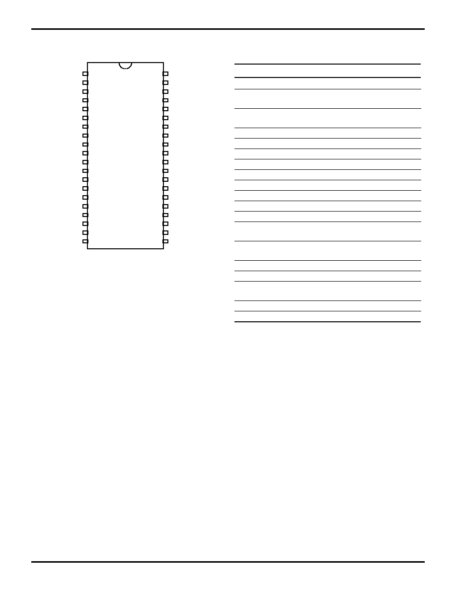
Figure 4. Z86C61 40-Pin DIP Pin Assignments
VCC
XTAL2
XTAL1
P37
P30
/RESET
R//W
/DS
/AS
P35
GND
P32
P00
P01
P02
P03
P04
P05
P06
P07
P36
P31
P27
P26
P25
P24
P23
P22
P21
P20
P33
P34
P17
P16
P15
P14
P13
P12
P11
P10
21
DIP 40 - Pin
1
20
40
Table 1. Z86C61 40-Pin DIP Pin Identification
Pin #
Symbol
Function
Direction
1
V
CC
Power Supply
Input
2
XTAL2
Crystal, Oscillator
Clock
Output
3
XTAL1
Crystal, Oscillator
Clock
Input
4
P37
Port 3, Pin 7
Output
5
P30
Port 3, Pin 0
Input
6
/RESET
Reset
Input
7
R//W
Read/Write
Output
8
/DS
Data Strobe
Output
9
/AS
Address Strobe
Output
10
P35
Port 3, Pin 5
Output
11
GND
Ground
Input
12
P32
Port 3, Pin 2
Input
13-20 P07-P00
Port 0, Pins
0,1,2,3,4,5,6,7
In/Output
21-28 P17-P10
Port 1, Pins
0,1,2,3,4,5,6,7
In/Output
29
P34
Port 3, Pin 4
Output
30
P33
Port 3, Pin 3
Input
31-38 P27-P20
Port 2, Pins
0,1,2,3,4,5,6,7
In/Output
39
P31
Port 3, Pin 1
Input
40
P36
Port 3, Pin 6
Output
PS003501-0301

Z86C61/62/96
CMOS Z8 Microcontroller
Zilog
6
P R E L I M I N A R Y
DS97Z8X1600
PIN DESCRIPTION (Continued)
Figure 5. Z86C61 44-Pin PLCC Pin Assignments
PLCC 44 - Pin
7
17
/RESET
R//W
/DS
/AS
P35
GND
P32
P00
P01
P02
R//RL
NC
P24
P23
P22
P21
P20
P33
P34
P17
P16
P15
1
28
18
40
39
29
6
Table 2. Z86C61 44-Pin PLCC Pin Assignments
Pin #
Symbol
Function
Direction
1
V
CC
Power Supply
Input
2
XTAL2
Crystal, Oscillator Clock Output
3
XTAL1
Crystal, Oscillator Clock Input
4
P37
Port 3, Pin 7
Output
5
P30
Port 3, Pin 0
Input
6
N/C
Not Connected
Input
7
/RESET
Reset
Input
8
R//W
Read/Write
Output
9
/DS
Data Strobe
Output
10
/AS
Address Strobe
Output
11
P35
Port 3, Pin 5
Output
12
GND
Ground
Input
13
P32
Port 3, Pin 2
Input
14-16 P02-P00
Port 0, Pins 0,1,2
In/Output
17
R//RL
ROM/ROMless control
Input
18-22 P07-P03
Port 0, Pins 3,4,5,6,7
In/Output
23-27 P14-P10
Port 1, Pins 0,1,2,3,4
In/Output
28
N/C
Not Connected
Input
29-31 P17-P15
Port 1, Pins 5,6,7
In/Output
32
P34
Port 3, Pin 4
Output
33
P33
Port 3, Pin 3
Input
34-38 P24-P20
Port 2, Pins 0,1,2,3,4
In/Output
39
N/C
Not Connected
Input
40-42 P25-P27
Port 2, Pins 5,6,7
In/Output
43
P31
Port 3, Pin 1
Input
44
P36
Port 3, Pin 6
Output
Table 2. Z86C61 44-Pin PLCC Pin Assignments
Pin #
Symbol
Function
Direction
PS003501-0301

Z86C61/62/96
Zilog
CMOS Z8 Microcontroller
DS97Z8X1600
P R E L I M I N A R Y
7
1
Figure 6. Z86C62/C96 64-Pin DIP Pin Assignments
P44
VCC
P45
XTAL2
XTAL1
P37
P30
NC
/RESET
R//W
/DS
P46
P47
/AS
P35
R//RL
GND
P32
P50
P51
P00
P01
P02
P03
P04
P05
P06
P07
VCC
P52
P53
P54
P43
P42
P36
P31
P41
P40
P27
P26
P25
P24
P23
P22
P60
P61
P21
P20
GND
P33
P34
P62
P63
P17
P16
P15
P14
P13
P12
P57
P56
P11
P10
P55
64
33
32
1
Table 3. Z86C62/C96 64-Pin DIP Pin Identification
Pin #
Symbol
Function
Direction
1
P44
Port 4, Pin 4
In/Output
2
V
CC
Power Supply
Input
3
P45
Port 4, Pin 5
In/Output
4
XTAL2
Crystal, Oscillator
Clock
Output
5
XTAL1
Crystal, Oscillator
Clock
Input
6
P37
Port 3, Pin 7
Output
7
P30
Port 3, Pin 0
Input
8
N/C
Not Connected
Input
9
/RESET
Reset
Input
10
R//W
Read/Write
Output
11
/DS
Data Strobe
Output
12-13
P47-P46
Port 4, Pin 6,7
In/Output
14
/AS
Address Strobe
Output
15
P35
Port 3, Pin 5
Output
16
R//RL
ROM/ROMless
control
Input
17
GND
Ground
Input
18
P32
Port 3, Pin 2
Input
19-20
P51-P50
Port 5, Pin 0,1
In/Output
21-28
P07-P00
Port 0, Pins
0,1,2,3,4,5,6,7
In/Output
29
V
CC
Power Supply
Input
30-33
P52-P55
Port 5, Pins 2,3,4,5 In/Output
34-35
P11-P10
Port 1, Pins 0,1
In/Output
36-37
P57-P56
Port 5, Pins 6,7
In/Output
38-43
P17-P12
Port 1, Pins
2,3,4,5,6,7
In/Output
44-45
P63-P62
Port 6, Pins 3,2
In/Output
46
P34
Port 3, Pin 4
Output
47
P33
Port 3, Pin 3
Input
48
GND
Ground
Input
49-50
P21-P20
Port 2, Pins 0,1
In/Output
51-52
P61-P60
Port 6, Pins 1,0
In/Output
53-58
P27-P22
Port 2, Pins
2,3,4,5,6,7
In/Output
59-60
P41-P40
Port 4, Pins 0,1
In/Output
61
P31
Port 3, Pin 1
Input
62
P36
Port 3, Pin 6
Output
63
P42
Port 4, Pin 2
In/Output
64
P43
Port 4, Pin 3
In/Output
PS003501-0301

Z86C61/62/96
CMOS Z8 Microcontroller
Zilog
8
P R E L I M I N A R Y
DS97Z8X1600
PIN DESCRIPTION (Continued)
Figure 7. Z86C62/C96 68-Pin PLCC Pin Assignments
60
44
10
26
R//W
/PODS
/DS
P46
P47
/P1DS
/AS
/DTimers
P35
R//RL
GND
P32
P50
P51
P00
P01
P02
43
27
61
9
PLCC 68 - Pin
1
P24
P23
P22
P60
P61
P21
P20
SCLK
/SYNC
GND
P33
P34
P62
P63
P17
P16
P15
PS003501-0301
Z86C61/62/96
Zilog
CMOS Z8 Microcontroller
DS97Z8X1600
P R E L I M I N A R Y
9
1
Table 4. Z86C62/C96 68-Pin PLCC Pin Identification
Pin #
Symbol
Function
Direction
1-2
P44-P43
Port 4, Pins 3,4
In/Output
3
V
CC
Power Supply
Input
4
P45
Port 4, Pin 5
In/Output
5
XTAL2
Crystal, Oscillator Clock
Output
6
XTAL1
Crystal, Oscillator Clock
Input
7
P37
Port 3, Pin 7
Output
8
P30
Port 3, Pin 0
Input
9
/RESET
Reset
Input
10
R//W
Read/Write
Output
11
/P0DS
Port 0 Data Strobe
Output
12
/DS
Data Strobe
Output
13-14
P47-P46
Port 4, Pins 6,7
In/Output
15
/P1DS
Port 1, Data Strobe
Output
16
/AS
Address Strobe
Output
17
/DTIMER
DTIMER
Input
18
P35
Port 3, Pin 5
Output
19
R//RL
ROM/ROMless control
Input
20
GND
Ground
Input
21
P32
Port 3, Pin 2
Input
22-23
P51-P50
Port 5, Pins 0,1
In/Output
24-31
P07-P00
Port 0, Pins 0,1,2,3,4,5,6,7
In/Output
32
V
CC
Power Supply
Input
33-36
P55-P52
Port 5, Pins 2,3,4,5
In/Output
37-38
P11-P10
Port 1, Pins 0,1
In/Output
39-40
P56-P57
Port 5, Pins 6,7
In/Output
41-46
P17-P12
Port 1, Pins2,3,4,5,6,7
In/Output
47-48
P63-P62
Port 6, Pins 3,2
In/Output
49
P34
Port 3, Pin 4
Output
50
P33
Port 3, Pin 3
Input
51
GND
Ground
Input
52
/SYNC
Synchronization
Output
53
SCLK
System Clock
Output
54-55
P21-P20
Port 2, Pins 0,1
In/Output
56-57
P60-P61
Port 6, Pins 1,0
In/Output
58-63
P27-P22
Port 2, Pins 2,3,4,5,6,7
In/Output
64-65
P41-P40
Port 4, Pins 0,1
In/Output
66
P31
Port 3, Pin 1
Input
67
P36
Port 3, Pin 6
Output
68
P42
Port 4, Pin 2
In/Output
PS003501-0301

Z86C61/62/96
CMOS Z8 Microcontroller
Zilog
10
P R E L I M I N A R Y
DS97Z8X1600
ABSOLUTE MAXIMUM RATINGS
Stresses greater than those listed under Absolute Maxi-
mum Ratings may cause permanent damage to the de-
vice. This is a stress rating only; operation of the device at
any condition above those indicated in the operational sec-
tions of these specifications is not implied. Exposure to ab-
solute maximum rating conditions for an extended period
may affect device reliability.
STANDARD TEST CONDITIONS
The characteristics listed below apply for standard test
conditions as noted. All voltages are referenced to GND.
Positive current flows into the referenced pin (Figure 4).
Sym
Description
Min
Max
Units
V
CC
Supply Voltage*
≠0.3
+7.0
V
T
STG
Storage Temp
≠65
+150
C
T
A
Oper Ambient Temp
Notes:
*Voltages on all pins with respect to GND.
See ordering information
Figure 8. Test Load Diagram
I
PS003501-0301

Z86C61/62/96
Zilog
CMOS Z8 Microcontroller
DS97Z8X1600
P R E L I M I N A R Y
11
1
DC ELECTRICAL CHARACTERISTICS
Z86C61/62/96
T
A
= 0∞C to +70∞C
T
A
= -40∞C to +105∞C Typical
Sym
Parameter
Min
Max
Min
Max
@ 25∞C Units
Conditions
Max Input Voltage
7
7
V
I
IN
< 250 µA
V
CH
Clock Input High
Voltage
0.85 V
CC
V
CC
+ 0.3
0.85 V
CC
V
CC
+ 0.3
V
Driven by External
Clock Generator
V
CL
Clock Input Low
Voltage
V
SS
≠ 0.3
0.8
V
SS
≠ 0.3
0.8
V
Driven by External
Clock Generator
V
IH
Input High Voltage
2
V
CC
+ 0.3
2
V
CC
+ 0.3
V
V
IL
Input Low Voltage
V
SS
≠ 0.3
0.2 V
CC
V
SS
≠ 0.3
0.2 V
CC
V
V
OH
Output High Voltage
2.4
2.4
V
I
OH
= ≠2.0 mA
V
OH
Output High Voltage
V
CC
≠ 100
mV
V
CC
≠ 100
mV
V
I
OH
= ≠100 µA
V
OL
Output Low Voltage
0.4
0.4
V
I
OL
= +5.0 mA [3]
V
OL
Output Low Voltage
0.6
0.6
V
I
OL
= +4.0 mA [2]
V
RH
Reset Input High
Voltage
0.85 V
CC
V
CC
+ 0.3
0.85 V
CC
V
CC
+ 0.3
V
V
Rl
Reset Input Low
Voltage
≠0.3
0.2 V
CC
≠0.3
0.2 V
CC
V
I
IL
Input Leakage
≠2
2
≠2
2
µA
V
IN
= 0V, V
CC
I
OL
Output Leakage
≠2
2
≠2
2
µA
V
IN
= 0
V
, V
CC
I
IR
Reset Input Current
≠80
≠80
µA
VRL = 0 V
I
CC
Supply Current
35
35
24
mA
[1] @ 16 MHz
I
CC
Supply Current
40
40
30
mA
[1] @ 20 MHz
I
CC1
Standby Current
15
15
4.5
mA
[1] HALT Mode
V
IN
= 0 V, V
CC
@
16 MHz
I
CC2
Standby Current
10
20
5
µA
[1] STOP Mode
V
IN
= 0 V, V
CC
Notes:
1. All inputs driven to either 0V or V
CC
, outputs floating.
2. V
CC
= 3.0V to 3.6V
3. V
CC
= 4.5V to 5.5V
PS003501-0301

Z86C61/62/96
CMOS Z8 Microcontroller
Zilog
12
P R E L I M I N A R Y
DS97Z8X1600
DC ELECTRICAL CHARACTERISTICS (Continued)
Figure 9. External I/O or Memory Read/Write
R//W
Port 0, /DM
Port 1
/AS
/DS
(Read)
Port 1
/DS
(Write)
A7 - A0
D7 - D0 IN
D7 - D0 OUT
A7 - A0
PS003501-0301

Z86C61/62/96
Zilog
CMOS Z8 Microcontroller
DS97Z8X1600
P R E L I M I N A R Y
13
1
AC CHARACTERISTICS
External I/O or Memory Read and Write Timing
Z86C61/62/96 (16 MHz)
T
A
= 0∞C to
+70∞C
T
A
= -40∞C to
+105∞C
16 MHz
16 MHz
No
Symbol
Parameter
Min
Max
Min
Max
Units
Notes
1
TdA(AS)
Address Valid to /AS rise Delay
25
25
ns
2,3
2
TdAS(A)
/AS rise to Address Float Delay
35
35
ns
2,3
3
TdAS(DR)
/AS rise to Read Data Req'd Valid
150
150
ns
1,2,3
4
TwAS
/AS Low Width
40
40
ns
2,3
5
TdAZ(DS)
Address Float to /DS fall
0
0
ns
6
TwDSR
/DS (Read) Low Width
135
135
ns
1,2,3
7
TwDSW
/DS (Write) Low Width
80
80
ns
1,2,3
8
TdDSR(DR)
/DS fall to Read Data Req'd Valid
75
75
ns
1,2,3
9
ThDR(DS)
Read Data to /DS rise Hold Time
0
0
ns
2,3
10
TdDS(A)
/DS rise to Address Active Delay
50
50
ns
2,3
11
TdDS(AS)
/DS rise to /AS fall Delay
35
35
ns
2,3
12
TdR/W(AS)
R//W Valid to /AS rise Delay
25
25
ns
2,3
13
TdDS(R/W)
/DS rise to R//W Not Valid
35
35
ns
2,3
14
TdDW(DSW)
Write Data Valid to /DS fall (Write)
Delay
25
25
ns
2,3
15
TdDS(DW)
/DS rise to Write Data Not Valid
Delay
35
35
ns
2,3
16
TdA(DR)
Address Valid to Read Data Req'd
Valid
210
210
ns
1,2,3
17
TdAS(DS)
/AS rise to /DS fall Delay
45
45
ns
2,3
18
TdDM(AS)
/DM Valid to /AS rise Delay
25
25
ns
2,3
Notes:
1. When using extended memory timing add 2 TpC.
2. Timing numbers given are for minimum TpC.
3. See clock cycle dependent characteristics table.
Standard Test Load
All timing references use 2.0 V for a logic 1 and 0.8 V for a logic 0.
Table 5. Clock Dependent Formulas
Number
Symbol
Equation
1
TdA(AS)
0.40 TpC + 0.32
2
TdAS(A)
0.59 TpC ≠ 3.25
3
TdAS(DR)
2.83 TpC + 6.14
4
TwAS
0.66 TpC ≠ 1.65
6
TwDSR
2.33 TpC ≠ 10.56
7
TwDSW
1.27 TpC + 1.67
8
TdDSR(DR)
1.97 TpC ≠ 42.5
10
TdDS(A)
0.8 TpC
11
TdDS(AS)
0.59 TpC ≠ 3.14
12
TdR/W(AS)
0.4 TpC
13
TdDS(R/W)
0.8 TpC ≠ 15
14
TdDW(DSW)
0.4 TpC
15
TdDS(DW)
0.88 TpC ≠ 19
16
TdA(DR)
4 TpC ≠ 20
17
TdAS(DS)
0.91 TpC ≠ 10.7
18
TdDM(AS)
0.9 TpC ≠ 26.3
Table 5. Clock Dependent Formulas
Number
Symbol
Equation
PS003501-0301
Z86C61/62/96
CMOS Z8 Microcontroller
Zilog
14
P R E L I M I N A R Y
DS97Z8X1600
AC CHARACTERISTICS
External I/O or Memory Read and Write Timing
Z86C61/62/96 (20 MHz)
T
A
= 0∞C to +70∞C
T
A
= -40∞C to +105∞C
20 MHz
20 MHz
No
Sym
Parameter
Min
Max
Min
Max
Units
Notes
1
TdA(AS)
Address Valid to /AS rise
Delay
15
25
ns
2,3
2
TdAS(A)
/AS rise to Address Float
Delay
25
35
ns
2,3
3
TdAS(DR)
/AS rise to Read Data
Req'd Valid
120
120
ns
1,2,3
4
TwAS
/AS Low Width
30
30
ns
2,3
5
TdAZ(DS)
Address Float to /DS fall
0
0
ns
6
TwDSR
/DS (Read) Low Width
105
105
ns
1,2,3
7
TwDSW
/DS (Write) Low Width
65
65
ns
1,2,3
8
TdDSR(DR)
/DS fall to Read Data
Req'd Valid
55
55
ns
1,2,3
9
ThDR(DS)
Read Data to /DS rise Hold
Time
0
0
ns
2,3
10
TdDS(A)
/DS rise to Address Active
Delay
40
40
ns
2,3
11
TdDS(AS)
/DS rise to /AS fall Delay
25
25
ns
2,3
12
TdR/W(AS)
R//W Valid to /AS rise
Delay
20
20
ns
2,3
13
TdDS(R/W)
/DS rise to R//W Not Valid
25
25
ns
2,3
14
TdDW(DSW)
Write Data Valid to /DS fall
(Write) Delay
20
20
ns
2,3
15
TdDS(DW)
/DS rise to Write Data Not
Valid Delay
25
25
ns
2,3
16
TdA(DR)
Address Valid to Read
Data Req'd Valid
150
150
ns
1,2,3
17
TdAS(DS)
/AS rise to /DS fall Delay
35
35
ns
2,3
18
TdDM(AS)
/DM Valid to /AS rise Delay
15
15
ns
2,3
Notes:
1. When using extended memory timing add 2 TpC.
2. Timing numbers given are for minimum TpC.
3. See clock cycle dependent characteristics table.
PS003501-0301

Z86C61/62/96
Zilog
CMOS Z8 Microcontroller
DS97Z8X1600
P R E L I M I N A R Y
15
1
AC CHARACTERISTICS
Additional Timing Diagram
Figure 10. Additional Timing
Clock
1
3
4
8
2
2
3
TIN
IRQN
6
5
7
7
9
PS003501-0301

Z86C61/62/96
CMOS Z8 Microcontroller
Zilog
16
P R E L I M I N A R Y
DS97Z8X1600
AC CHARACTERISTICS
Additional Timing Table
Z86C61/62/96
T
A
= 0∞C to +70∞C
TA = -40∞C to +105∞C
20/16 MHz
20/16 MHz
No
Symbol
Parameter
Min
Max
Min
Max
Units
Notes
1
TpC
Input Clock Period
50/62.5
1000
50/62.5
1000
ns
1
2
TrC,TfC
Clock Input Rise & Fall
Times
10
10
ns
1
3
TwC
Input Clock Width
25
25
ns
1
4
TwTinL
Timer Input Low Width
75
75
ns
2
5
TwTinH
Timer Input High Width
5 TpC
5 TpC
ns
2
6
TpTin
Timer Input Period
8 TpC
8 TpC
ns
2
7
TrTin,TfTin Timer Input Rise and
Fall Times
100
100
ns
2
8a
TwIL
Interrupt Request Input
Low Times
70
50
ns
2,4
8b
TwIL
Interrupt Request Input
Low Times
5 TpC
5 TpC
ns
2,5
9
TwIH
Interrupt Request Input
High Times
5 TpC
5 TpC
ns
2,3
Notes:
1. Clock timing references use 0.8V
CC
for a logic 1 and 0.8V for a logic 0.
2. Timing references use 2.0V for a logic 1 and 0.8V for a logic 0.
3. Interrupt references request through Port 3.
4. Interrupt request through Port 3 (P33-P31).
5. Interrupt request through Port 30.
PS003501-0301
Z86C61/62/96
Zilog
CMOS Z8 Microcontroller
DS97Z8X1600
P R E L I M I N A R Y
17
1
AC CHARACTERISTICS
Handshake Timing Diagrams
Figure 11. Input Handshake Timing
Data In
1
2
3
4
5
6
/DAV
(Input)
RDY
(Output)
Next Data In Valid
Delayed RDY
Delayed DAV
Data In Valid
Figure 12. Output Handshake Timing
Data Out
/DAV
(Output)
RDY
(Input)
Next Data Out Valid
Delayed RDY
Delayed DAV
Data Out Valid
7
8
9
10
11
PS003501-0301

Z86C61/62/96
CMOS Z8 Microcontroller
Zilog
18
P R E L I M I N A R Y
DS97Z8X1600
AC CHARACTERISTICS
Handshake Timing Table
Z86C61/62/96
T
A
= 0∞C to +70∞C
T
A
= ≠40∞C to
+105∞C
20/16 MHz
20/16 MHZ
Data
No
Symbol
Parameter
Min
Max
Min
Max
Direction
1
TsDI(DAV)
Data In Setup Time
0
0
IN
2
ThDI(DAV)
Data In Hold Time
145
145
IN
3
TwDAV
Data Available Width
110
110
IN
4
TdDAVI(RDY)
DAV fall to RDY fall Delay
115
115
IN
5
TdDAVId(RDY)
DAV rise to RDY rise Delay
115
115
IN
6
TdRDY0(DAV)
RDY rise to DAV fall Delay
0
0
IN
7
TdDO(DAV)
Data Out to DAV fall Delay
TpC
TpC
OUT
8
TdDAV0(RDY)
DAV fall to RDY fall Delay
0
0
OUT
9
TdRDY0(DAV)
RDY fall to DAV rise Delay
115
115
OUT
10
TwRDY
RDY Width
110
110
OUT
11
TdRDY0d(DAV)
RDY rise to DAV fall Delay
115
115
OUT
PS003501-0301

Z86C61/62/96
Zilog
CMOS Z8 Microcontroller
DS97Z8X1600
P R E L I M I N A R Y
19
1
PIN FUNCTIONS
R//RL (input, active Low). This pin when connected to
GND disables the internal ROM and forces the device to
function as a Z86C96 ROMless Z8. (Note: When left un-
connected or pulled High to VCC the part functions as a
normal Z86C61/62 ROM version.) This pin is only avail-
able on the 44-pin version of the Z86C61, and both ver-
sions of the Z86C62.
/DS (output, active Low). Data Strobe is activated once for
each external memory transfer. For a READ operation,
data must be available prior to the trailing edge of /DS. For
WRITE operations, the falling edge of /DS indicates that
output data is valid.
/AS (output, active Low). Address Strobe is pulsed once at
the beginning of each machine cycle. Address out-put is
through Port 1 for all external programs. Memory address
transfers are valid at the trailing edge of /AS. Under pro-
gram control, /AS can be placed in the high-impedance
state along with Ports 0 and 1, Data Strobe, and
Read/Write.
XTAL1, XTAL2 Crystal 1, Crystal 2 (time-based input and
output, respectively). These pins connect a parallel-reso-
nant crystal, ceramic resonator, LC, or any external single-
phase clock to the on-chip oscillator and buffer.
R//W (output, write Low). The Read/Write signal is Low
when the MCU is writing to the external program or data
memory.
/RESET (input, active Low). To avoid asynchronous and
noisy reset problems, the Z86C61/62/96 is equipped with
a reset filter of four external clocks (4TpC). If the external
/RESET signal is less than 4TpC in duration, no reset oc-
curs.
On the fifth clock after the /RESET is detected, an internal
RST signal is latched and held for an internal register
count of 18 external clocks, or for the duration of the exter-
nal /RESET, whichever is longer. During the reset cycle,
/DS is held active Low while /AS cycles at a rate of TpC/2.
When /RESET is deactivated, program execution begins
at location 000C (HEX). Reset time must be held Low for
50 ms, or until VCC is stable, whichever is longer.
/P0DS Port 0 Data Strobe (output, active Low). Signal
used to emulate Port 0 when in ROMless mode.
/P1DS Port 1 Data Strobe (output, active Low). Signal
used to emulate Port 1 when in ROMless mode.
/DTIMERS Disable Timers (input, active Low). All timers
are stopped by the Low level at this pin. This pin has an in-
ternal pull up resistor.
SCLK (output). System clock pin.
/SYNC Instruction SYNC Signal (output, active Low). This
signal indicates the last clock of the current executing in-
struction.
Port 0 (P07-P00). Port 0 is an 8-bit, nibble programmable,
bidirectional, TTL compatible port. These eight I/O lines
can be configured under software control as a nibble I/O
port, or as an address port for interfacing external memory.
When used as an I/O port, Port 0 may be placed under
handshake control. In this configuration, Port 3, lines P32
and P35 are used as the handshake control /DAV0 and
RDY0 (Data Available and Ready). Handshake signal as-
signment is dictated by the I/O direction of the upper nibble
P07-P04. The lower nibble must have the same direction
as the upper nibble to be under handshake control.
For external memory references, Port 0 can provide ad-
dress bits A11-A8 (lower nibble) or A15-A8 (lower and up-
per nibble) depending on the required address space. If
the address range requires 12 bits or less, the upper nibble
of Port 0 can be programmed independently as I/O while
the lower nibble is used for addressing. If one or both nib-
bles are needed for I/O operation, they must be configured
by writing to the Port 0 Mode register.
In ROMless mode, after a hardware reset, Port 0 lines are
defined as address lines A15-A8, and extended timing is
set to accommodate slow memory access. The initializa-
tion routine includes reconfiguration to eliminate this ex-
tended timing mode (Figure 14).
PS003501-0301
Z86C61/62/96
CMOS Z8 Microcontroller
Zilog
20
P R E L I M I N A R Y
DS97Z8X1600
PIN FUNCTIONS (Continued)
Figure 13. Port 0 Configuration
OEN
Out
In
PAD
Port 0 (I/O)
Handshake Controls
/DAV0 and RDY0
(P32 and P35)
MCU
4
TTL Level Shifter
Auto Latch
R
500 K
4
PS003501-0301

Z86C61/62/96
Zilog
CMOS Z8 Microcontroller
DS97Z8X1600
P R E L I M I N A R Y
21
1
Port 1 (P17-P10). Port 1 is an 8-bit, byte programmable,
bidirectional, TTL compatible port. It has multiplexed Ad-
dress (A7-A0) and Data (D7-D0) ports. For Z86C61/62/96,
these eight I/O lines can be programmed as Input or Out-
put lines or can be configured under software control as an
address/data port for interfacing external memory. When
used as an I/O port, Port 1 may be placed under hand-
shake control. In this configuration, Port 3 line P33 and
P34 are used as the handshake controls RDY1 and
/DAV1.
Memory locations greater than 16,384 are referenced
through Port 1. To interface external memory, Port 1 must
be programmed for the multiplexed Address/Data mode. If
more than 256 external locations are required, Port 0 must
output the additional lines.
Port 1 can be placed in high-impedance state along with
Port 0, /AS, /DS, and R//W, allowing the microcontroller to
share common resources in multiprocessor and DMA ap-
plications. Data transfers can be controlled by assigning
P33 as a Bus Acknowledge input, and P34 as a Bus re-
quest output (Figure 14).
Figure 14. Port 1 Configuration
OEN
Out
In
PAD
Port 1
(AD7-AD0)
MCU
TTL Level Shifter
Auto Latch
R
500 K
8
Handshake Controls
/DAV1 and RDY1
(P33 and P34)
PS003501-0301
Z86C61/62/96
CMOS Z8 Microcontroller
Zilog
22
P R E L I M I N A R Y
DS97Z8X1600
PIN FUNCTIONS (Continued)
Port 2 (P27-P20). Port 2 is an 8-bit, bit programmable, bi-
directional, CMOS-compatible port. Each of these eight
I/O lines can be independently programmed as an input or
output or globally as an open-drain output. Port 2 is always
available for I/O operation. When used as an I/O port, Port
2 may be placed under handshake control. In this configu-
ration, Port 3 lines P31 and P36 are used as the hand-
shake control lines /DAV2 and RDY2. The handshake sig-
nal assignment for Port 3 lines P31 and P36 is dictated by
the direction (input or output) assigned to P27 (Figure 15).
Figure 15. Port 2 Configuration
OEN
Out
In
PAD
Port 2 (I/O)
Handshake Controls
/DAV2 and RDY2
(P31 and P36)
MCU
TTL Level Shifter
Auto Latch
R
500 K
Open-Drain
PS003501-0301

Z86C61/62/96
Zilog
CMOS Z8 Microcontroller
DS97Z8X1600
P R E L I M I N A R Y
23
1
Port 3 (P37-P30). Port 3 is an 8-bit, CMOS-compatible
four-fixed input and four-fixed output port. These eight I/O
lines have four-fixed (P33-P30) input and four-fixed (P37-
P34) output ports. Port 3, when used as serial I/O, are pro-
grammed as serial in and serial out, respectively (Figure
16).
Figure 16. Port 3 Configuration
Out
In
PAD
MCU
Port 3
(I/O or Control)
Auto Latch
R
500 K
PAD
Port 3 Output Configuration
Port 3 Input Configuration
PS003501-0301

Z86C61/62/96
CMOS Z8 Microcontroller
Zilog
24
P R E L I M I N A R Y
DS97Z8X1600
PIN FUNCTIONS (Continued)
Port 3 can be configured under software control to provide
the following control functions: handshake for Ports 0 and
2 (/DAV and RDY); four external interrupt request signals
(IRQ3-IRQ0); timer input and output signals (T
IN
and
T
OUT
), and Data Memory Select (/DM).
Uart Operation
Port 3 lines P30 and P37, can be programmed as serial I/O
lines for full-duplex serial asynchronous receiver/transmit-
ter operation. The bit rate is controlled by the
Counter/Timer0.
The Z86C61/62/96 automatically adds a start bit and two
stop bits to transmitted data (Figure 17). Odd parity is also
available as an option. Eight data bits are always transmit-
ted, regardless of parity selection. If parity is enabled, the
eighth bit is the odd parity bit. An interrupt request (IRQ4)
is generated on all transmitted characters.
Received data must have a start bit, eight data bits and at
least one stop bit. If parity is on, bit 7 of the received data
is replaced by a parity error flag. Received characters gen-
erate the IRQ3 interrupt request.
Note: UART function is only available in standard timing
mode (i.e., P01M D5 = 0).
Table 6. Port 3 Pin Assignments
Pin
I/O
CTC1
Int.
P0 HS
P1 HS
P2 HS
UART
Ext
P30
IN
IRQ3
Serial In
P31
IN
T
IN
IRQ2
D/R
P32
IN
IRQ0
D/R
P33
IN
IRQ1
D/R
P34
OUT
R/D
DM
P35
OUT
R/D
P36
OUT
T
OUT
R/D
P37
OUT
Serial Out
T0
IRQ4
T1
IRQ5
Notes:
HS = Handshake Signals
D = Data Available
R = Ready
PS003501-0301

Z86C61/62/96
Zilog
CMOS Z8 Microcontroller
DS97Z8X1600
P R E L I M I N A R Y
25
1
Figure 17. Serial Data Formats
D7
D6
D5
D4
D3
D2
D1
D0
Start Bit
Eight Data Bits
Transmitted Data (No Parity)
Two Stop Bits
SP SP
ST
D7
D6
D5
D4
D3
D2
D1
D0
Start Bit
Eight Data Bits
Received Data (No Parity)
One Stop Bit
SP
ST
P
D6
D5
D4
D3
D2
D1
D0
Start Bit
Seven Data Bits
Transmitted Data (With Parity)
Odd Parity
Two Stop Bits
SP SP
ST
P
D6
D5
D4
D3
D2
D1
D0
Start Bit
Seven Data Bits
Received Data (With Parity)
Parity Error Flag
One Stop Bit
ST
SP
PS003501-0301

Z86C61/62/96
CMOS Z8 Microcontroller
Zilog
26
P R E L I M I N A R Y
DS97Z8X1600
PIN FUNCTIONS (Continued)
Port 4 (P47-P40). Port 4 is an 8-bit, bit programmable, bi-
directional, CMOS-compatible port. Each of these eight
I/O lines can be independently programmed as an input or
output or globally as an open-drain output. Port 4 is always
available for I/O operation (Figure 18). Port address (F)02.
Port 5 (P57-P50). Same as Port 4. Port address (F)04.
Port 6 (P63-P60). Same as Port 4. (Note: this is a 4-bit
port, bits D3-D0.) Port address (F)07.
Auto Latch. The Auto Latch puts valid CMOS levels on all
CMOS inputs that are not externally driven. This reduces
excessive supply current flow in the input buffer when it is
not being driven by any source.
Figure 18. Port 4 Configuration
OEN
Out
In
PAD
Port 4 (I/O)
MCU
TTL Level Shifter
Auto Latch
R
500 K
Open-Drain
PS003501-0301
Z86C61/62/96
Zilog
CMOS Z8 Microcontroller
DS97Z8X1600
P R E L I M I N A R Y
27
1
FUNCTIONAL DESCRIPTION
Address Space
Program Memory. The Z86C61/62 can address up to 48
KB of external program memory (Figure 19). The first 12
bytes of program memory are reserved for the interrupt
vectors. These locations contain six 16-bit vectors that cor-
respond to the six available interrupts. For ROM mode,
byte 13 to byte 16383 consists of on-chip ROM. At ad-
dresses 16384 and greater, the Z86C61/62 executes ex-
ternal program memory fetches. The Z86C96, and the
Z86C61/62 in ROMless mode, can address up to 64 KB of
external program memory. Program execution begins at
external location 000CH after a reset.
Data Memory (/DM). The ROM version can address up to
48 KB of external data memory space beginning at loca-
tion 16384. The ROMless version can address up to 64 KB
of external data memory. External data memory may be in-
cluded with, or separated from, the external program
memory space. /DM, an optional I/O function that can be
programmed to appear on pin P34, is used to distinguish
between data and program memory space (Figure 20).
The state of the /DM signal is controlled by the type in-
struction being executed. An LDC opcode references
PROGRAM (/DM inactive) memory, and an LDE instruc-
tion references DATA (/DM active Low) memory.
Figure 19. Program Memory Configuration
12
11
10
9
8
7
6
5
4
3
2
1
0
External
ROM and RAM
Location of
First Byte of
Instruction
Executed
After RESET
Interrupt
Vector
(Lower Byte)
Interrupt
Vector
(Upper Byte)
IRQ5
IRQ4
IRQ4
IRQ3
IRQ3
IRQ2
IRQ2
IRQ1
IRQ1
IRQ0
IRQ0
IRQ5
65535
On-Chip ROM
16384
16383
Figure 20. Data Memory Configuration
65535
16384
16383
0
External
Data
Memory
Not Addressable
PS003501-0301
Z86C61/62/96
CMOS Z8 Microcontroller
Zilog
28
P R E L I M I N A R Y
DS97Z8X1600
FUNCTIONAL DESCRIPTION (Continued)
Register File. The Register File consists of four I/O port
registers, 236 general-purpose registers and 16 control
and status registers (Figure 18). There are eight further
registers for I/O ports 4, 5 and 6 in the Expanded Register
File (Bank F, R9-R2) (Figure 20).
The instructions can access registers directly or indirectly
through an 8-bit address field. The Z86C61/62/96 also al-
lows short 4-bit register addressing using the Register
Pointer (Figure 21). In the 4-bit mode, the Register File is
divided into 16 working register groups, each occupying 16
continuous locations. The Register Pointer addresses the
starting location of the active working-register group.
Note: Register Bank E0-EF can only be accessed through
working registers and indirect addressing modes.
Figure 21. Register Pointer Register
D7
D6
D5
D4
D3
D2
D1
D0
Expanded Register Group
Working Register Group
RP
R253
Default Setting After Reset = 00000000
Figure 22. Register File
Stack Pointer (Bits 7-0)
R255
Stack Pointer (Bits 15-8)
Register Pointer
Program Control Flags
Interrupt Mask Register
Interrupt Request Register
Interrupt Priority Register
Ports 0-1 Mode
Port 3 Mode
Port 2 Mode
T0 Prescaler
Timer/Counter0
T1 Prescaler
Timer/Counter1
Timer Mode
Serial I/O
General-Purpose
Registers
Port 3
Port 2
Port 1
Port 0
R254
R253
R252
R251
R250
R249
R248
R247
R246
R245
R244
R243
R242
R241
R240
R239
R3
R2
R1
R0
SPL
SPH
RP
FLAGS
IMR
IRQ
IPR
P01M
P3M
P2M
PRE0
T0
PRE1
T1
TMR
SIO
P3
P2
P1
P0
R4
Location
Identifiers
PS003501-0301
Z86C61/62/96
Zilog
CMOS Z8 Microcontroller
DS97Z8X1600
P R E L I M I N A R Y
29
1
Figure 23. Expanded Register File Architecture
PS003501-0301

Z86C61/62/96
CMOS Z8 Microcontroller Zilog
30 P R E L I M I N A R Y DS97Z8X1600
FUNCTIONAL DESCRIPTION (Continued)
Expanded Register File. The register file has been ex-
panded to allow for additional system control registers,
and for mapping of additional peripheral devices along
with I/O ports into the register address area. The Z8 regis-
ter address space R0 through R15 has now been imple-
mented as 16 groups of 16 registers per group. These reg-
ister groups are known as the ERF (Expanded Register
File). Bits 7-4 of Register RP select the working register
group. Bits 3-0 of Register RP select the expanded register
group (Figure 21). Eight I/O port registers reside in the Ex-
panded Register File at Bank F. The rest of the Expanded
Register is not physically implemented and is open for fu-
ture expansion.
The upper nibble of the register pointer (Figure 20) selects
which group of 16 bytes in the register file, out of the full
236, will be accessed. The lower nibble selects the ex-
panded register file bank and in the case of the
Z86C61/62/96, only Bank F is implemented. A 0H in the
lower nibble will allow the normal register file to be ad-
dressed, but any other value from 1H to FH will exchange
the lower 16 registers in favor of an expanded register
group of 16 registers.
For example:
Z86C61: (See Figures 21 and 22)
R253 RP = 00H R0 = Port 0 R2 = Port 2
R1 = Port 1 R3 = Port 3
But If:
R253 RP = 0FH R0 = Reserved
R1 = Reserved
R2 = Port 4
R3 = Port 4, Direction Register
R9 = Port 6, Mode Register
Further examples:
SRP #0FH Set working group 0 and Bank F
LD R2, #10010110 Load value into Port 4 using
working register addressing.
LD 2, #10010110 Load value into Port 4 using
absolute addressing.
LD 9, #11110000 Load value into Port 6 mode.
SRP #1FH Set working group 1 and Bank F
LD R2, #11010110 Load value into general purpose
register 12H
LD 12H, #11010110 Load value into general purpose
register 12H
LD 2, #10010110 Load value into Port 4
RAM Protect. The upper portion of the RAM's address
spaces 80FH to EFH (excluding the control registers) can
be protected from reading and writing. The RAM Protect bit
option is mask-programmable and is selected by the cus-
tomer when the ROM code is submitted. After the mask
option is selected, the user can activate from the internal
ROM code to turn off/on the RAM Protect by loading a bit
D6 in the IMR register to either a 0 or a 1, respectively. A
1 in D6 indicates RAM Protect enabled.
ROM Protect. The first 16 Kbytes of program memory is
mask programmable. A ROM protect feature prevents
"dumping" of the ROM contents by inhibiting execution of
LDC, LDCI, LDE, and LDEI instructions by external pro-
gram memory when pointing to internal memory locations.
Therefore these instructions can be used only when they
are executed from internal memory, or if they are executed
from external memory and pointing to external memory lo-
cations.
The ROM Protect option is mask-programmable, to be se-
lected by the customer at the time when the ROM code is
submitted.
PS003501-0301
Z86C61/62/96
Zilog
CMOS Z8 Microcontroller
DS97Z8X1600
P R E L I M I N A R Y
31
1
Stack. The Z86C61/62/96 has a 16-bit Stack Pointer
(R255-R254) used for external stack that resides any-
where in the data memory for the ROMless mode, but only
from 16384 to 65535 in the ROM mode. An 8-bit Stack
Pointer (R255) is used for the internal stack that resides
within the 236 general-purpose registers (R239-R4). The
high byte of the Stack Pointer (SPH-Bit 8-15) can be used
as a general purpose register when using internal stack
only.
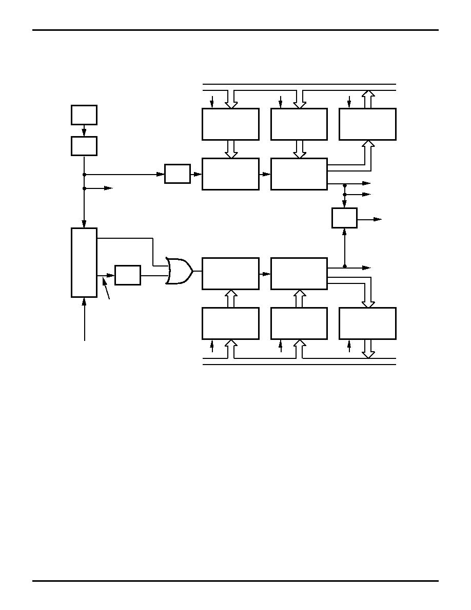
Counter/Timers. There are two 8-bit programmable
counter/timers (T0-T1), each driven by its own 6-bit pro-
grammable prescaler. The T1 prescaler can be driven by
internal or external clock sources; however, the T0 pres-
caler is driven by the internal clock only (Figure 22).
The 6-bit prescalers can divide the input frequency of the
clock source by any integer number from 1 to 64. Each
prescaler drives its counter, which decrements the value
(1 to 256) that has been loaded into the counter. When
both the counters and prescaler reach the end of the
count, a timer interrupt request, IRQ4 (T0) or IRQ5 (T1), is
generated.
The counter can be programmed to start, stop, restart to
continue, or restart from the initial value. The counters can
also be programmed to stop upon reaching zero (single
pass mode) or to automatically reload the initial value and
continue counting (modulo-n continuous mode).
The counter, but not the prescalers, can be read at any
time without disturbing their value or count mode. The
clock source for T1 is user-definable and can be either the
internal microprocessor clock divided-by-four, or an exter-
nal signal input through Port 3. The Timer Mode register
configures the external timer input (P31) as an external
clock, a trigger input that can be retriggerable or non-retrig-
gerable, or as a gate input for the internal clock. Port 3, line
P36, also serves as a timer output (TOUT) through which
T0, T1 or the internal clock can be output. The counter/tim-
ers can be cascaded by connecting the T0 output to the in-
put of T1.
Figure 24. Register Pointer
The upper nibble of the register file address
provided by the register pointer specifies
the active working-register group.
r7
r6
r5
r4
R253
(Register Pointer)
I/O Ports
Specified Working
Register Group
The lower nibble
of the register
file address
provided by the
instruction points
to the specified
register.
r3
r2
r1
r0
Register Group 1
Register Group 0
R15 to R0
Register Group F
R15 to R4
R3 to R0
R15 to R0
∑
∑
∑
∑
∑
FF
F0
0F
00
1F
10
2F
20
∑
∑
∑
∑
∑
∑
∑
∑
∑
PS003501-0301
Z86C61/62/96
CMOS Z8 Microcontroller
Zilog
32
P R E L I M I N A R Y
DS97Z8X1600
FUNCTIONAL DESCRIPTION (Continued)
Figure 25. Counter/Timer Block Diagram
OSC
PRE0
Initial Value
Register
T0
Initial Value
Register
T0
Current Value
Register
6-Bit
Down
Counter
8-bit
Down
Counter
˜4
6-Bit
Down
Counter
8-Bit
Down
Counter
PRE1
Initial Value
Register
T1
Initial Value
Register
T1
Current Value
Register
˜2
Clock
Logic
IRQ4
IRQ5
Internal Data Bus
Write
Write
Read
Internal Clock
Gated Clock
Triggered Clock
TIN P31
Write
Write
Read
Internal Data Bus
External Clock
Internal
Clock
˜4
Serial I/O
Clock
Tout
P36
˜2
PS003501-0301

Z86C61/62/96
Zilog
CMOS Z8 Microcontroller
DS97Z8X1600
P R E L I M I N A R Y
33
1
Interrupts. The Z86C61/62/96 has six different interrupts
from eight different sources. The interrupts are maskable
and prioritized. The eight sources are divided as follows:
four sources are claimed by Port 3 lines P33-P30, one in
Serial Out, one is Serial In, and two in the counter/timers
(Figure 26). The Interrupt Mask Register globally or indi-
vidually enables or disables the six interrupt requests.
When more than one interrupt is pending, priorities are re-
solved by a programmable priority encoder that is con-
trolled by the Interrupt Priority register. All Z86C61/62/96
interrupts are vectored through locations in the program
memory. When an interrupt machine cycle is activated, an
interrupt request is granted. Thus, this disables all of the
subsequent interrupts, saves the Program Counter and
Status Flags, and then branches to the program memory
vector location reserved for that interrupt. This memory lo-
cation and the next byte contain the 16-bit address of the
interrupt service routine for that particular interrupt re-
quest.
To accommodate polled interrupt systems, interrupt inputs
are masked and the Interrupt Request register is polled to
determine which of the interrupt requests need service.
Software initialed interrupts are supported by setting the
appropriate bit in the Interrupt Request Register (IRQ).
Internal interrupt requests are sampled on the falling edge
of the last cycle of every instruction. The interrupt request
must be valid 5TpC before the falling edge of the last clock
cycle of the currently executing instruction.
For the ROMless mode, when the device samples a valid
interrupt request, the next 48 (external) clock cycles are
used to prioritize the interrupt, and push the two PC bytes
and the FLAG register onto the stack. The following nine
cycles are used to fetch the interrupt vector from external
memory. The first byte of the interrupt service routine is
fetched beginning on the 58th TpC cycle following the in-
ternal sample point, which corresponds to the 63rd TpC
cycle following the external interrupt sample point.
Figure 26. Interrupt Block Diagram
IRQ
IMR
IPR
PRIORITY
LOGIC
6
Global
Interrupt
Enable
Vector Select
Interrupt
Request
IRQ0 - IRQ5
PS003501-0301

Z86C61/62/96
CMOS Z8 Microcontroller
Zilog
34
P R E L I M I N A R Y
DS97Z8X1600
FUNCTIONAL DESCRIPTION (Continued)
Clock. The Z86C61/62/96 on-chip oscillator has a high-
gain, parallel-resonant amplifier for connection to a crystal,
LC, ceramic resonator, or any suitable external clock
source (XTAL1 = Input, XTAL2 = Output). The crystal
should be AT cut, 1 MHz to 20 MHz max, and series resis-
tance (RS) is less than or equal to 100 Ohms. The crystal
should be connected across XTAL1 and XTAL2 using the
recommended capacitors (10 pF < CL < 100 pF) from each
pin to device ground (Figure 27).
Note: Actual capacitor values specified by the crystal
manufacturer.
HALT. Turns off the internal CPU clock but not the XTAL
oscillation. The counter/timers and the external interrupts
IRQ0, IRQ1, IRQ2, and IRQ3 remain active. The devices
are recovered by interrupts, either externally or internally
generated. An interrupt request must be executed (en-
abled) to exit HALT mode. After the interrupt service rou-
tine, the program continues from the instruction after the
HALT.
STOP. This instruction turns off the internal clock and ex-
ternal crystal oscillation and reduces the standby current
to 5 µA (typical) or less. The STOP mode is terminated by
a reset, which causes the processor to restart the applica-
tion program at address 000CH.
In order to enter STOP (or HALT) mode, it is necessary to
first flush the instruction pipeline to avoid suspending exe-
cution in mid-instruction. To do this, the user must execute
a NOP (opcode=0FFH) immediately before the appropri-
ate sleep instruction, i.e.,
Figure 27. Oscillator Configuration
XTAL1
XTAL2
C1
C2
C1
C2
XTAL1
XTAL2
XTAL1
XTAL2
Ceramic Resonator
or Crystal
LC Clock
External Clock
L
FF
NOP
; clear the pipeline
6F
STOP
; enter STOP mode
or
FF
NOP
; clear the pipeline
7F
HALT
; enter HALT mode
PS003501-0301

Z86C61/62/96
Zilog
CMOS Z8 Microcontroller
DS97Z8X1600
P R E L I M I N A R Y
35
1
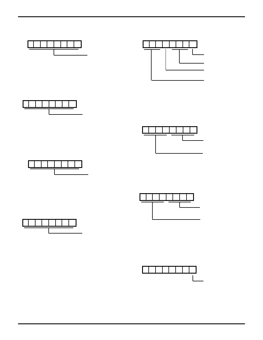
Z8 CONTROL REGISTER DIAGRAMS
Figure 28. Serial I/O Register
(F0H: Read/Write)
Figure 29. Timer Mode Register
(F1H: Read/Write)
Figure 30. Counter/Timer1 Register
(F2H: Read/Write)
D7
D6
D5
D4
D3
D2
D1
D0
Serial Data (D0 = LSB)
R240 SIO
D7
D6
D5
D4
D3
D2
D1
D0
0 Disable T0 Count
1 Enable T0 Count
0 No Function
1 Load T0
0 No Function
1 Load T1
0 Disable T1 Count
1 Enable T1 Count
T
IN
Modes
00 External Clock Input
01 Gate Input
10 Trigger Input
(Non-retriggerable)
11 Trigger Input
(Retriggerable)
T
OUT
Modes
00 Not Used
01 T0 Out
10 T1 Out
11 Internal Clock Out
R241 TMR
D7
D6
D5
D4
D3
D2
D1
D0
T1 Initial Value
(When Written)
(Range: 1-256 Decimal
01-00 HEX)
T1 Current Value
(When Read)
R242 T1
Figure 31. Prescaler 1 Register
(F3H: Write Only)
Figure 32. Counter/Timer 0 Register
(F4H: Read/Write)
Figure 33. Prescaler 0 Register
(F5H: Write Only)
D7
D6
D5
D4
D3
D2
D1
D0
Count Mode
0 T1 Single Pass
1 T1 Modulo N
Clock Source
1 T1 Internal
0 T1 External Timing Input
(T
IN
) Mode
Prescaler Modulo
(Range: 1-64 Decimal
01-00 HEX)
R243 PRE1
D7
D6
D5
D4
D3
D2
D1
D0
T0 Initial Value
(When Written)
(Range: 1-256 Decimal
01-00 HEX)
T0 Current Value
(When Read)
R244 T0
0 T0 Single Pass
1 T0 Modulo N
D7
D6
D5
D4
D3
D2
D1
D0
Count Mode
Reserved (Must be 0)
Prescaler Modulo
(Range: 1-64 Decimal
01-00 HEX)
R245 PRE0
PS003501-0301

Z86C61/62/96
CMOS Z8 Microcontroller
Zilog
36
P R E L I M I N A R Y
DS97Z8X1600
Z8 CONTROL REGISTER DIAGRAMS (Continued)
Figure 34. Port 2 Mode Register
(F6H: Write Only)
Figure 35. Port 3 Mode Register
(F7H: Write Only)
D7
D6
D5
D4
D3
D2
D1
D0
P2
0
- P2
7
I/O Definition
0 Defines Bit as Output
1 Defines Bit as Input
R246 P2M
D7
D6
D5
D4
D3
D2
D1
D0
R247 P3M
0 Port 2 Open Drain
1 Port 2 Push-pull
0 Parity Off
1 Parity On
0 P32 = Input
P35 = Output
1 P32 = /DAV0/RDY0
P35 = RDY0//DAV0
0 P31 = Input (TIN)
P36 = Output (TOUT)
1 P31 = /DAV2/RDY2
P36 = RDY2//DAV2
0 P30 = Input
P37 = Output
1 P30 = Serial In
P37 = Serial Out
Reserved (Must be 0)
00 P33 = Input
P34 = Output
01 P33 = Input
10 P34 = /DM
P33 = /DAV1/RDY1
P34 = RDY1//DAV1
11
Figure 36. Port 0 and 1 Mode Register
(F8H: Write Only)
Figure 37. Interrupt Priority Register
(F9H: Write Only)
D7
D6
D5
D4
D3
D2
D1
D0
R248 P01M
P0
0
- P0
0
Mode
00 Output
01 Input
1X A
11
- A
8
Stack Selection
0 External
1 Internal
P1
7
- P1
0
Mode
00 Byte Output
01 Byte Input
10 AD
7
- AD
0
11 High-Impedance AD
7
- DA
0
,
/AS, /DS, /R//W, A
11
- A
8
,
A
15
- A
12
, If Selected
P0
7
- P0
4
Mode
00 Output
01 Input
1X A
15
- A
12
Reserved (Must be 0)
D7
D6
D5
D4
D3
D2
D1
D0
Interrupt Group Priority
Reserved = 000
C > A > B = 001
A > B > C = 010
A > C > B = 011
B > C > A = 100
C > B > A = 101
B > A > C = 110
Reserved = 111
IRQ3, IRQ5 Priority (Group A)
0 IRQ5 > IRQ3
1 IRQ3 > IRQ5
IRQ0, IRQ2 Priority (Group B)
0 IRQ2 > IRQ0
1 IRQ0 > IRQ2
IRQ1, IRQ4 Priority (Group C)
0 IRQ1 > IRQ4
1 IRQ4 > IRQ1
Reserved (Must be 0)
R249 IPR
PS003501-0301

Z86C61/62/96
Zilog
CMOS Z8 Microcontroller
DS97Z8X1600
P R E L I M I N A R Y
37
1
Figure 38. Interrupt Request Register
(FAH: Read/Write)
Figure 39. Interrupt Mask Register
(FBH: Read/Write)
Figure 40. Flag Register
(FCH: Read/Write)
D7
D6
D5
D4
D3
D2
D1
D0
R250 IRQ
Reserved (Must be 0)
IRQ0 = P32 Input (D0 = IRQ0)
IRQ1 = P33 Input
IRQ2 = P31 Input
IRQ3 = P30 Input, Serial Input
IRQ4 = T0 Serial Output
IRQ5 = T1
D7
D6
D5
D4
D3
D2
D1
D0
1 Enables RAM Protect
1 Enables IRQ5-IRQ0
(D
0
= IRQ0)
1 Enables Interrupts
R251 IMR
D7
D6
D5
D4
D3
D2
D1
D0
R252 FLAGS
User Flag F1
User Flag F2
Half Carry Flag
Decimal Adjust Flag
Overflow Flag
Sign Flag
Zero Flag
Carry Flag
Figure 41. Register Pointer Register
(FDH: Read/Write)
Figure 42. Stack Pointer Register
(FEH: Read/Write)
Figure 43. Stack Pointer Register
(FFH: Read/Write)
D7
D6
D5
D4
D3
D2
D1
D0
R253 RP
Expanded Register Pointer
Working Register Pointer
D7
D6
D5
D4
D3
D2
D1
D0
Stack Pointer Upper
Byte (SP
15
- SP
8
)
R254 SPH
D7
D6
D5
D4
D3
D2
D1
D0
Stack Pointer Lower
Byte (SP
7
- SP
0
)
R255 SPL
PS003501-0301
Z86C61/62/96
CMOS Z8 Microcontroller
Zilog
38
P R E L I M I N A R Y
DS97Z8X1600
Z8 EXPANDED REGISTER FILE CONTROL REGISTERS
Figure 44. Port 4 Data Register
(F) 02: Read/Write)
Figure 45. Port 4 Mode Register
(F( 03: (Write Only)
Figure 46. Port 5 Data Register
(f) 04: (Read/Write)
Figure 47. Port 5 Mode Register
(F) 05: (Write Only)
D7 D6
D5
D4
D3
D2 D1
D0
Data
0 Defines Level 0
1 Defines Level 1
P4 (FH) 02H
D7
D6
D5
D4
D3
D2
D1
D0
P40 - P47 I/O Definition
0 Defines Bit as Output
1 Defines Bit as Input
P4M (FH) 03H
D7 D6
D5
D4 D3
D2
D1
D0
P5 (FH) 04H
Data
0 Defines Level 0
1 Defines Level 1
P50 - P57 I/O Definition
0 Defines Bit as Output
1 Defines Bit as Input*
P5D (FH) 05H
D7 D6
D5
D4
D3
D2 D1
D0
*Default Value After RESET
Figure 48. Port 4/5 Configuration Register
(F) 06: (Write Only)
Figure 49. Port 6 Data Register
(F) 07: (Read/Write)
Figure 50. Port 6 Mode Register
(F) 08: (Write Only)
Figure 51. Port 6 Mode Register
(F) 09: (Write Only)
D4
D0
P45M (FH) 06H
0 Port 4 Open-drain*
1 Port 4 Push-pull
Reserved (Must be 0)
0 Port 5 Open-drain*
1 Port 5 Push-pull
Reserved (Must be 0)
*Default Value After RESET
D7
D6
D5
D4
D3
D2
D1
D0
P6 (FH) 07H
Reserved (Must be 0)
Data
0 Defines Level 0
1 Defines Level 1
D3
D2
D1
D0
P60 - P63 I/O Definition
0 Defines Bit as Output
1 Defines Bit as Input*
P6D (FH) 08H
Reserved (Must be 0)
*Default Value After RESET
D7
D6
D5
D4
D3
D2
D1
D0
0 Port 6 Open-drain*
1 Port 6 Push-pull
P6M (FH) 09H
*Default Value After RESET
PS003501-0301
Z86C61/62/96
Zilog
CMOS Z8 Microcontroller
DS97Z8X1600
P R E L I M I N A R Y
39
1
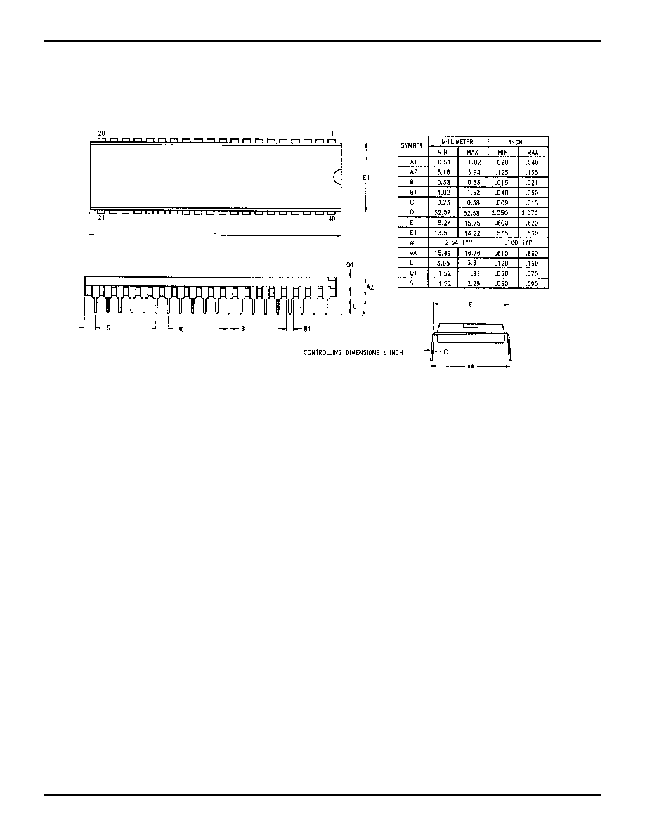
PACKAGE INFORMATION
Figure 52. 40-Pin DIP Package Diagram
Figure 53. 44-Pin PLCC Package Diagram
PS003501-0301

Z86C61/62/96
CMOS Z8 Microcontroller
Zilog
40
P R E L I M I N A R Y
DS97Z8X1600
PACKAGE INFORMATION (Continued)
Figure 54. 64-Pin DIP Package Diagram
PS003501-0301

Z86C61/62/96
Zilog
CMOS Z8 Microcontroller
DS97Z8X1600
P R E L I M I N A R Y
41
1
Figure 55. 68-Pin PLCC Package Diagram
PS003501-0301

Z86C61/62/96
CMOS Z8 Microcontroller
Zilog
42
P R E L I M I N A R Y
DS97Z8X1600
ORDERING INFORMATION
Z86C61/62/96
For fast results, contact your Zilog sales office for assis-
tance in ordering the part desired.
Codes
Package
P = Plastic DIP
V = Plastic Chip Carrier
Preferred Temperature
S = 0∞C to +70∞C
Longer Lead Time
E = -40∞C to 105∞C
Speeds
16 = 16 MHz
20 = 20 MHz
Environmental
C = Plastic Standard
© 1997 by Zilog, Inc. All rights reserved. No part of this
document may be copied or reproduced in any form or by
any means without the prior written consent of Zilog, Inc.
The information in this document is subject to change
without notice. Devices sold by Zilog, Inc. are covered by
warranty and patent indemnification provisions appearing
in Zilog, Inc. Terms and Conditions of Sale only.
ZILOG, INC. MAKES NO WARRANTY, EXPRESS,
STATUTORY, IMPLIED OR BY DESCRIPTION,
REGARDING THE INFORMATION SET FORTH HEREIN
OR REGARDING THE FREEDOM OF THE DESCRIBED
DEVICES FROM INTELLECTUAL PROPERTY
INFRINGEMENT. ZILOG, INC. MAKES NO WARRANTY
OF MERCHANTABILITY OR FITNESS FOR ANY
PURPOSE.
Zilog, Inc. shall not be responsible for any errors that may
appear in this document. Zilog, Inc. makes no commitment
to update or keep current the information contained in this
document.
Zilog's products are not authorized for use as critical
components in life support devices or systems unless a
specific written agreement pertaining to such intended use
is executed between the customer and Zilog prior to use.
Life support devices or systems are those which are
intended for surgical implantation into the body, or which
sustains life whose failure to perform, when properly used
in accordance with instructions for use provided in the
labeling, can be reasonably expected to result in
significant injury to the user.
Zilog, Inc. 210 East Hacienda Ave.
Campbell, CA 95008-6600
Telephone (408) 370-8000
FAX 408 370-8056
Internet: http://www.zilog.com
16 MHz
40-pin DIP
44-pin PLCC
Z86C6116PSC
Z86C6116VSC
16 MHz
64-pin DIP
68-pin PLCC
Z86C6216PSC
Z86C6216VSC
20 MHz
64-pin DIP
68-pin PLCC
Z86C9620PSC
Z86C9620VSC
Example:
Z 86C61 16 P S C is a Z86C61, 16 MHz, DIP, 0∞ to +70∞C, Plastic Standard Flow
Environmental Flow
Temperature
Package
Speed
Product Number
Zilog Prefix
PS003501-0301