 | –≠–ª–µ–∫—Ç—Ä–æ–Ω–Ω—ã–π –∫–æ–º–ø–æ–Ω–µ–Ω—Ç: Z86C65 | –°–∫–∞—á–∞—Ç—å:  PDF PDF  ZIP ZIP |
1
P R E L I M I N A R Y
Z86C60/65
CP96Z8X0400
FEATURES
ROM
RAM*
Speed 28-pin
Part
(KB)
(Bytes)
I/O
(MHz)
DIP
Z86C60
1 6
256
2 2
1 6
X
Z86C65
3 2
256
2 2
1 6
X
s
Low EMI Mode Option
s
Auto Latches
s
Two Programmable 8-Bit Counter/Timers Each with 6-
Bit Programmable Prescaler
s
Three Vectored, Priority Interrupts from Three Different
Sources
s
On-Chip Oscillator that Accepts a Crystal Ceramic
Resonator, LC, or External Clock Source
s
ROM Mask Options:
≠ ROM Protect
≠ RAM Protect
*General-Purpose
s
28-Pin DIP Package
s
3.0V to 5.5V Operating Range
s
Low-Power Consumption: 200 mW
s
Fast Instruction Pointer: 0.75
µ
s @ 16 MHz
s
Two Standby Modes: STOP and HALT
P
RELIMINARY
C
USTOMER
P
ROCUREMENT
S
PECIFICATION
Z86C60/65
CMOS Z8
Æ
32K ROM M
ICROCONTROLLER
The Z86C60/65 microcontrollers introduce a new level of
sophistication to single-chip architecture. The Z86C65 is a
member of the Z8 single-chip microcontroller family with
32 Kbytes of ROM and 256 bytes of RAM. The Z86C60 is
identical, except that it only has 16 Kbytes of ROM.
The Z86C60/65 are housed in a 28-pin DIP package, and
manufactured in CMOS technology. The Z86C96 ROMless
Z8 will support the Z86C60/65.
Zilog's CMOS microcontroller offers fast execution, more
efficient use of memory, more sophisticated interrupts,
input/output bit manipulation capabilities, and easy hard-
ware/software system expansion along with low cost and
low power consumption.
The Z86C60/65 architecture is characterized by Zilog's
8-bit microcontroller core. The device offers a flexible I/O
scheme, an efficient register and address space structure,
multiplexed capabilities between address/data, I/O, and a
number of ancillary features that are useful in many indus-
trial and advanced scientific applications.
For applications which demand powerful I/O capabilities,
the Z86C60/65 fulfills this with 22 pins dedicated to input
and output. These lines are grouped into four ports. Each
port is configurable under software control to provide
timing, status signals, serial or parallel I/O with or without
handshake, and an address/data bus for interfacing exter-
nal memory.
There are three basic address spaces available to support
this wide range of configurations: Program Memory, Data
Memory, and 236 General-Purpose Registers.
To unburden the program from coping with the real-time
problems such as counting/timing and serial data commu-
nication, the Z86C60/65 offers two on-chip counter/timers
with a large number of user selectable modes.
Notes:
All Signals with a preceding front slash, "/", are active Low, e.g.,
B//W (WORD is active Low); /B/W (BYTE is active Low, only).
Power connections follow conventional descriptions below:
Connection
Circuit
Device
Power
V
CC
V
DD
Ground
GND
V
SS
CP96Z8X0400 (5/96)
GENERAL DESCRIPTION
2
P R E L I M I N A R Y
Z86C60/65
CP96Z8X0400
GENERAL DESCRIPTION
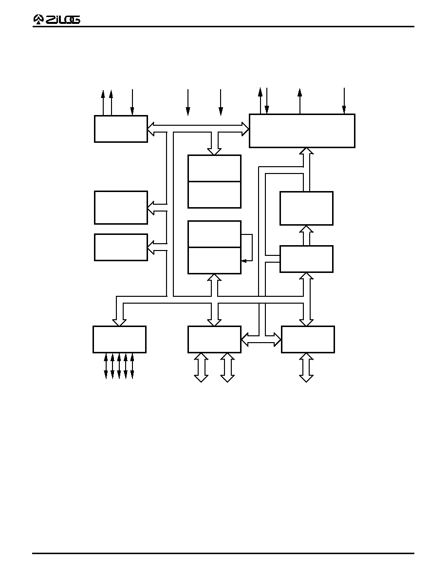
Figure 1. Z86C60/65 Functional Block Diagram
Port 3
Counter/
Timers
(2)
Interrupt
Control
Port 2
I/O
(Bit Programmable)
ALU
FLAGS
Register
Pointer
Register File
Machine Timing and
Instruction Control
Prg. Memory
Program
Counter
Vcc
GND
XTAL
2
4
Port 0
Output
Input
Address or I/O
(Nibble Programmable)
Port 1
8
Address/Data or I/O
(Byte Programmable)
/DS
/RESET
3
P R E L I M I N A R Y
Z86C60/65
CP96Z8X0400
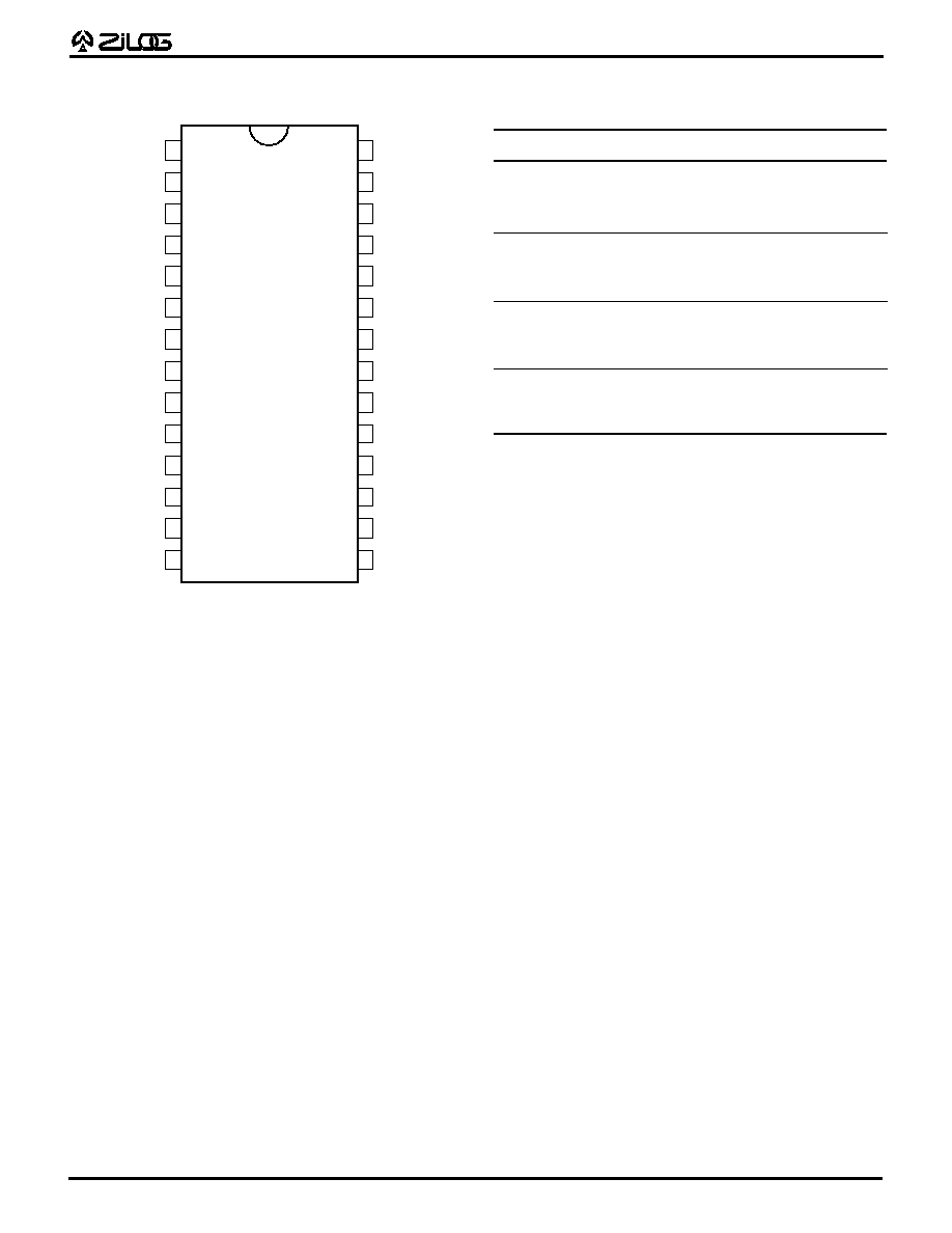
Z86C60/65 28-Pin DIP Pin Identification
Pin #
Symbol
Function
Direction
1
V
CC
Power Supply
Input
2
XTAL2
Crystal, Oscillator Clock
Output
3
XTAL1
Crystal, Oscillator Clock
Input
4
/RESET
Reset
Input
5
/DS
Data Strobe
Output
6
P35
Port 3, Pin 5
Output
7
GND
Ground
Input
8-13
P05-P00
Port 0, Pins 0,1,2,3,4,5
In/Output
14-21
P17-P10
Port 1, Pins 0,1,2,3,4,5,6,7 In/Output
22-26
P25-P21
Port 2, Pins 1,2,3,4,5
In/Output
2 7
P31
Port 3, Pin 1
Input
2 8
P36
Port 3, Pin 6
Output
PIN DESCRIPTION
Figure 2. Z86C60/65 28-Pin DIP
Pin Assignments
1
2
9
3
4
5
6
7
8
28
27
26
25
24
23
22
21
20
P36
P31
P16
P25
P24
P23
P22
P21
P17
VCC
XTAL2
RESET
/DS
P35
GND
P00
19
18
17
16
15
14
10
11
12
13
XTAL1
P03
P04
P05
P10
P15
P14
P13
P12
P11
P01
P02
4
P R E L I M I N A R Y
Z86C60/65
CP96Z8X0400
STANDARD TEST CONDITIONS
The characteristics listed below apply for standard test
conditions as noted. All voltages are referenced to GND.
Positive current flows into the referenced pin (Test Load).
ABSOLUTE MAXIMUM RATINGS
Symbol
Description
Min
Max
Units
V
CC
Supply Voltage*
≠0.3
+7.0
V
T
STG
Storage Temp
≠65
+150
C
T
A
Oper Ambient Temp
Notes:
* Voltages on all pins with respect to GND.
See ordering information
Stresses greater than those listed under Absolute Maxi-
mum Ratings may cause permanent damage to the de-
vice. This is a stress rating only; operation of the device at
any condition above those indicated in the operational
sections of these specifications is not implied. Exposure to
absolute maximum rating conditions for an extended pe-
riod may affect device reliability.
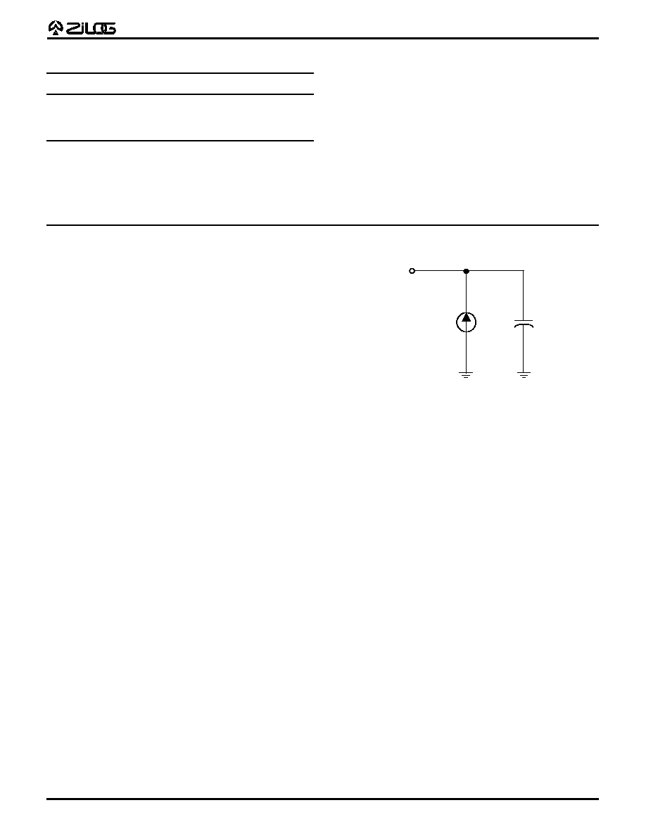
Figure 3. Test Load Diagram
From Output
Under Test
150 pF
I
5
P R E L I M I N A R Y
Z86C60/65
CP96Z8X0400
DC ELECTRICAL CHARACTERISTICS
Z86C60/65
T
A
= 0
∞
C
Typical
to +70
∞
C
at
Sym
Parameter
Min
Max
25
∞
C
Units
Conditions
V
CC
Operating Voltage
4.5
5.5
V
[3]
Max Input Voltage
7
V
[3] I
IN
< 250
µ
A
V
CH
Clock Input High Voltage
0.85 V
CC
V
CC
+ 0.3
V
Driven by External Clock Generator
V
CL
Clock Input Low Voltage
V
SS
≠ 0.3
0.8
V
Driven by External Clock Generator
V
IH
Input High Voltage
2
V
CC
+ 0.3
V
V
IL
Input Low Voltage
V
SS
≠ 0.3
0.2 V
CC
V
V
OH
Output High Voltage
2.4
V
CC
V
I
OH
= ≠2.0 mA
V
OH
Output High Voltage
V
CC
≠ 100 mV
V
I
OH
= ≠100
µ
A
V
OH
Output High Voltage (Low EMI)
2.4
V
I
OH
= ≠0.5 mA
V
OL
Output Low Voltage
0.4
V
I
OL
= +5.0 mA [2]
V
OL
Output Low Voltage (Low EMI)
0.4
V
I
OL
= +2.0 mA [2]
V
RH
Reset Input High Voltage
0.85 V
CC
V
CC
+ 0.3
V
V
Rl
Reset Input Low Voltage
≠0.3
0.2 V
CC
V
I
IL
Input Leakage
≠2
2
µ
A
V
IN
= 0 V, V
CC
I
OL
Output Leakage
≠2
2
µ
A
V
IN
= 0 V, V
CC
I
IR
Reset Input Current
≠180
µ
A
V
RL
= 0 V
I
CC
Supply Current (Standard Mode)
35
24
mA
[1] @ 16 MHz
I
CC
Supply Current (Low EMI)
6.0
4.0
mA
@ 4 MHz
I
CC1
Standby Current (Standard Mode)
15
4.5
mA
[1] HALT Mode V
IN
= 0 V, V
CC
@ 16 MHz
I
CC1
Standby Current (Low EMI)
1.6
0.8
mA
@ 4 MHz
I
CC2
Standby Current
10
5
µ
A
[1] STOP Mode V
IN
= 0 V, V
CC
I
ALL
Auto Latch Low Current
≠14
+14
5
µ
A
V
CC
= 5.0V
Notes:
[1]
All inputs driven to either 0V or V
CC
, outputs floating.
[2]
V
CC
= 4.5V to 5.5V
[3]
/Reset pin must be a maximum of V
CC
+ 0.3V.
6
P R E L I M I N A R Y
Z86C60/65
CP96Z8X0400
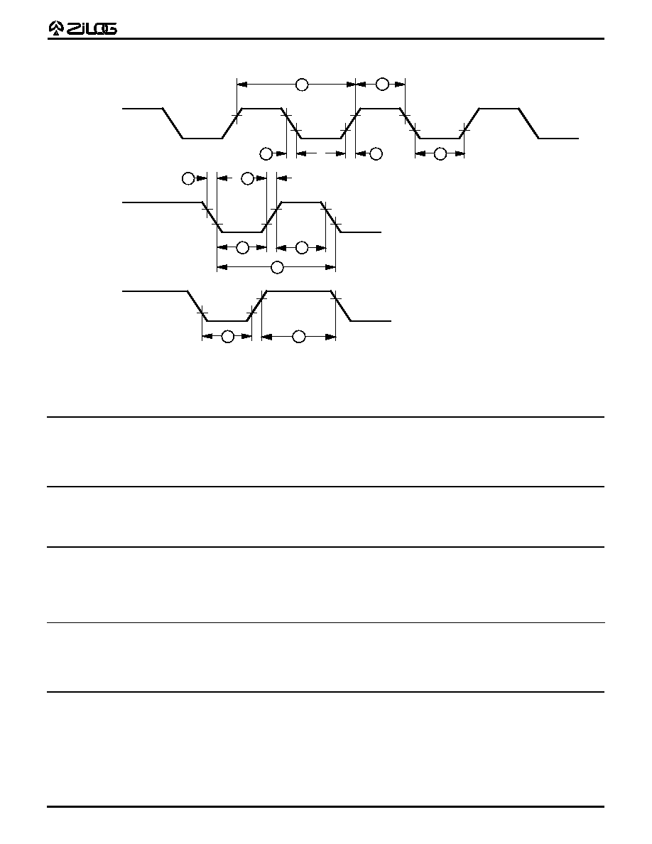
Clock
1
3
4
8
2
2
3
TIN
IRQN
6
5
7
7
9
Figure 4. Additional Timing
AC CHARACTERISTICS
Additional Timing Table
Z86C60/65 (Standard Mode Only)
T
A
= 0
∞
C
to +70
∞
C
16 MHz
No
Symbol
Parameter
Min
Max
Units
Notes
1
TpC
Input Clock Period
62.5
DC
n s
[1]
2
TrC,TfC
Clock Input Rise & Fall Times
1 0
n s
[1]
3
TwC
Input Clock Width
3 1
n s
[1]
4
TwTinL
Timer Input Low Width
7 5
n s
[2]
5
TwTinH
Timer Input High Width
5 TpC
n s
[2]
6
TpTin
Timer Input Period
8 TpC
n s
[2]
7
TrTin,TfTin
Timer Input Rise and Fall Times
100
n s
[2]
8 a
TwIL
Interrupt Request Input Low Times
7 0
n s
[2,4]
8 b
TwIL
Interrupt Request Input Low Times
5 TpC
n s
[2,5]
9
TwIH
Interrupt Request Input High Times
5 TpC
n s
[2,3]
Notes:
[1] Clock timing references use 0.85V
CC
for a logic 1 and 0.8V for a logic 0.
[2] Timing references use 2.0V for a logic 1 and 0.8V for a logic 0.
[3] Interrupt references request through Port 3.
[4] Interrupt request through Port 3 (P33-P31).
[5] Interrupt request through Port 30.
AC CHARACTERISTICS
Additional Timing Diagram
7
P R E L I M I N A R Y
Z86C60/65
CP96Z8X0400
© 1996 by Zilog, Inc. All rights reserved. No part of this document
may be copied or reproduced in any form or by any means
without the prior written consent of Zilog, Inc. The information in
this document is subject to change without notice. Devices sold
by Zilog, Inc. are covered by warranty and patent indemnification
provisions appearing in Zilog, Inc. Terms and Conditions of Sale
only. Zilog, Inc. makes no warranty, express, statutory, implied or
by description, regarding the information set forth herein or
regarding the freedom of the described devices from intellectual
property infringement. Zilog, Inc. makes no warranty of mer-
chantability or fitness for any purpose. Zilog, Inc. shall not be
responsible for any errors that may appear in this document.
Zilog, Inc. makes no commitment to update or keep current the
information contained in this document.
Zilog's products are not authorized for use as critical compo-
nents in life support devices or systems unless a specific written
agreement pertaining to such intended use is executed between
the customer and Zilog prior to use. Life support devices or
systems are those which are intended for surgical implantation
into the body, or which sustains life whose failure to perform,
when properly used in accordance with instructions for use
provided in the labeling, can be reasonably expected to result in
significant injury to the user.
Zilog, Inc. 210 East Hacienda Ave.
Campbell, CA 95008-6600
Telephone (408) 370-8000
FAX 408 370-8056
Internet: http://www.zilog.com
formance with some aspects of the CPS may be found,
either by Zilog or its customers in the course of further
application and characterization work. In addition, Zilog
cautions that delivery may be uncertain at times, due to
start-up yield issues.
Pre-Characterization Product:
The product represented by this CPS is newly introduced
and Zilog has not completed the full characterization of the
product. The CPS states what Zilog knows about this
product at this time, but additional features or non-con-