
DS96DZ80203
1
1
C
USTOMER
P
ROCUREMENT
S
PECIFICATION
FEATURES
s
28-Pin DIP, SOIC, and PLCC Packages
s
Clock Speed: 16 MHz
s
Three Expanded Register Groups
s
8-Channel, 8-Bit A/D Converter with Track and Hold,
and Unique R-Ladder A
GND
Offset Control
s
Z86C84 has two 8-Bit D/A Converters with
Programmable Gain Stages, 3
µ
s Settling Time
s
Six Vectored, Prioritized Interrupts from Six Different
Sources
s
Two Analog Comparator Inputs with Programmable
Interrupt Polarity
s
Two Programmable 8-Bit Timers, each with a 6-Bit
Programmable Prescaler
s
Auto Latch Mask Option for P00, P01, and P02
s
Power-On Reset (POR) Timer
s
Permanent Watch-Dog Timer (WDT) Mask Option
s
Software-Programmable Pull-Up Resistors
s
On-Chip Oscillator for Crystal, Resonator or LC
GENERAL DESCRIPTION
The Z86C83/C84 Consumer Controller Processors
(CCP
TM
) are full-featured members of the CMOS Z8 micro-
controller family offering a unique register-to-register ar-
chitecture that avoids accumulator bottlenecks for higher
code efficiency than RISC processors.
The Z86C83/C84 are designed to be used in a wide variety
of embedded control applications, such as appliances,
process controls, keyboards, security systems, battery
chargers, and automotive modules.
For applications requiring powerful I/O capabilities, the
Z86C83/C84 devices can have up to 21/17 (C83/C84
respectively) pins dedicated to input and output. These
lines are grouped into three ports, and are configured by
software to provide digital/analog I/O timing and status
signals.
An on-chip, half-flash 8-bit
±
1/2 Least Significant Bit (LSB)
A/D converter can multiplex up to eight analog inputs.
Unused analog inputs revert to standard digital I/O use.
Unique, programmable A
GND
offset control of the A/D
resistor ladder compresses the converter's dynamic range
for maximum effective 9-bit A/D resolution.
The Z86C84 has two 8-bit
±
1/2 LSB D/A converters. High
and low reference voltages provide precise control of the
output voltage range. Programmable gain for each D/A
converter provides a maximum effective 10-bit resolution
for many tasks.
On-chip 8-bit counter/timers with many user-selectable
modes simplify real-time tasks, such as counting, timing,
and generation of PWM signals.
The designer can prioritize six different maskable,
vectored, internal or external interrupts for efficient
interrupt handling and multitasking functions.
Z86C83/C84
1
Z8
Æ
MCU M
ICROCONTROLLERS
Device
ROM
(KB)
RAM*
(Bytes)
I/O
Lines
Voltage
Range
Z86C83
4
237
21
3.0V to 5.5V
Z86C84
4
237
17
3.0V to 5.5V
Note:
* General-Purpose
Z86C83/C84
Z8
Æ
MCU Microcontrollers
2
DS96DZ80203
GENERAL DESCRIPTION
(Continued)
By means of an expanded register file, the designer has
access to additional control registers for configuring per-
ipheral functions including the A/D and D/A converters,
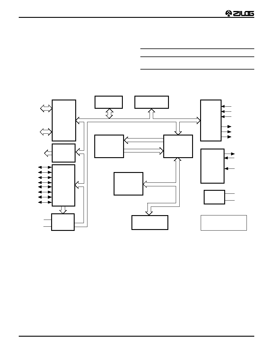
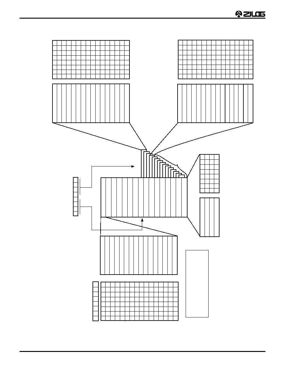
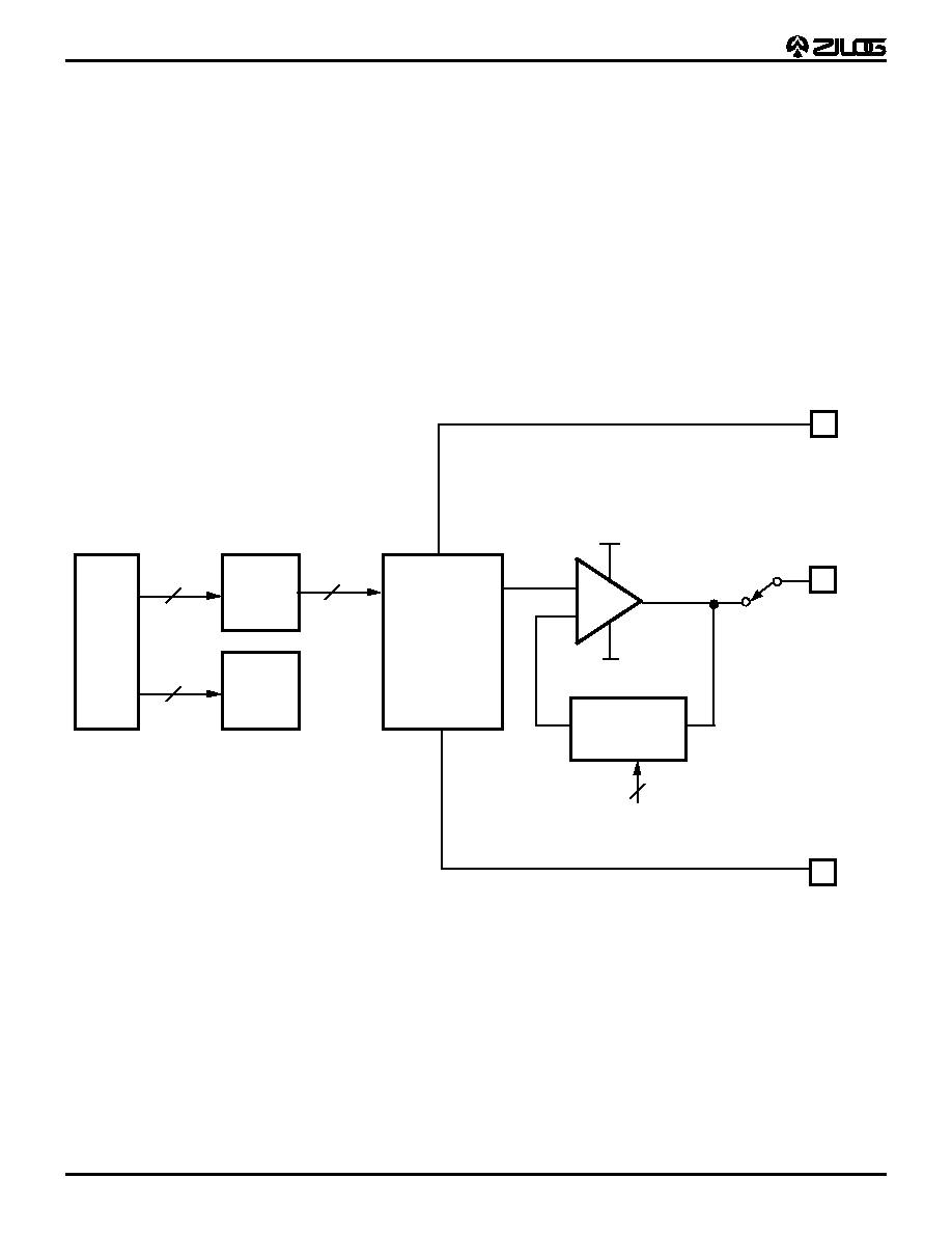
counter/timers, and I/O port functions (Figure 1).
Notes:
All Signals with a preceding front slash, "/", are
active Low, e.g., B//W (WORD is active Low); /B/W (BYTE
is active Low, only).
Power connections follow conventional descriptions
below:
Connection
Circuit
Device
Power
V
CC
V
CC
Ground
GND
V
SS
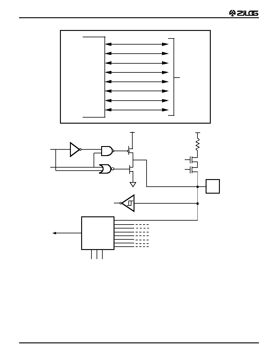
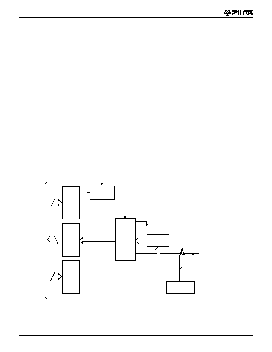
Figure 1. Z86C83/C84 Functional Block Diagram
Notes:
** Not available on Z86C83.
Not available on Z86C84.
Port 0
P00
P01
P02
P03
P04
P05
P06
P31
P32
P33
Port 3
Register File
256 x 8-Bit
ROM
4K x 8
Z8
Æ
Core
Register Bus
Internal
Address Bus
Internal Data Bus
Expanded
Register File
Expanded
Register Bus
Counter/Timer
8-Bit (2)
Machine
Timing
and
Instruction
Control
Power
XTAL 1/2
VCC
P34
P35
P36
AC0/P20
AC1/P21
AC2/P22
AC3/P23
AC4/P24
AC5/P25
AC6/P26
AC7/P27
Port 2
Comparators
(2)
/RESET
GND
8-Channel
8-Bit A/D
**Dual
8-Bit
DAC
AVCC
AGND
VDHI **
VDL0 **
DAC1 **
DAC2 **
Z86C83/C84
Z8
Æ
MCU Microcontrollers
DS96DZ80203
3
1
PIN DESCRIPTION
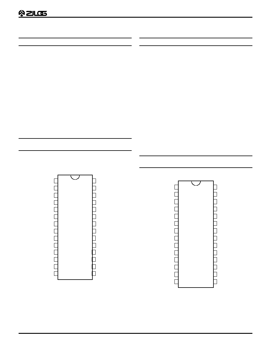
Table 1. Z86C83 28-Pin DIP, SOIC Pin Identification*
No
Symbol
Function
Direction
1-7
P21-P27
or AC1-AC7
Port 2, Bit 1-7
Analog In 1-7
Input/Output
8
/RESET
Reset
Input
9
XTAL1
Oscillator Clock
Input
10
XTAL2
Oscillator Clock
Output
11
GND
Ground
12
V
CC
Power
13-15
P31-P33
Port 3, Bits 1-3
Input
16
P34
Port 3, Bit 4
Output
17
P36
Port 3, Bit 6
Output
18
P35
Port 3, Bit 5
Output
19-25
P0-P06
Port 0, Bits 0-6
Input/Output
26
A
GND
Analog Ground
27
AV
CC
Analog Power
28
P20
or AC0
Port 2, Bit 0
Analog In 0
Input/Output
Note:
* DIP and SOIC Pin Description and Configuration are identical.
Figure 2. Z86C83 28-Pin DIP and SOIC Pin
Configuration*
1
2
9
3
4
5
6
7
8
28
27
26
25
24
23
22
21
20
P27/AC7
P26/AC6
AVCC
P25/AC5
P24/AC4
P23/AC3
P22/AC2
P21/AC1
P20/AC0
/RESET
XTAL1
P34
XTAL2
GND
VCC
P31
P32
P33
Z86C83
10
19
AGND
P36
13
11
12
18
17
16
P04
P06
P05
P01
P35
P00
14
15
P03
P02
Standard Mode
Table 2. Z86C84 28-Pin DIP, SOIC Pin Identification*
No
Symbol
Function
Direction
1-7
P21-P27
or AC1-AC7
Port 2, Bit 1-7
Analog In 1-7
Input/Output
8
/RESET
Reset
Input
9
XTAL1
Oscillator Clock
Input
10
XTAL2
Oscillator Clock
Output
11
GND
Ground
12
V
CC
Power
13-15 P31-P33
Port 3, Bits 1-3
Input
16
P34
Port 3, Bit 4
Output
17
P36
Port 3, Bit 6
Output
18
P35
Port 3, Bit 5
Output
19-21 P0-P02
Port 0, Bits 0-3
Input/Output
22
VDLO
D/A Ref. Volt.,Low
Input
23
VDHI
D/A Ref. Volt.,High
Input
24-25 DAC2-1
D/A Converter
Output
26
A
GND
Analog Ground
27
AV
CC
Analog Power
28
P20
or AC0
Port 2, Bit 0
Analog In 0
Input/Output
Note:
* DIP and SOIC Pin Description and Configuration are identical
Figure 3. Z86C84 28-Pin DIP and SOIC Pin
Configuration*
1
2
9
3
4
5
6
7
8
28
27
26
25
24
23
22
21
20
P27/AC7
P26/AC6
AVCC
P25/AC5
P24/AC4
P23/AC3
P22/AC2
P21/AC1
P20/AC0
/RESET
XTAL1
P34
XTAL2
GND
VCC
P31
P32
P33
Z86C84
10
19
AGND
P36
13
11
12
18
17
16
VDHI
DAC1
P01
P35
P00
14
15
VDLO
P02
* Standard Mode
DAC2
Z86C83/C84
Z8
Æ
MCU Microcontrollers
4
DS96DZ80203
PIN DESCRIPTION
(Continued)
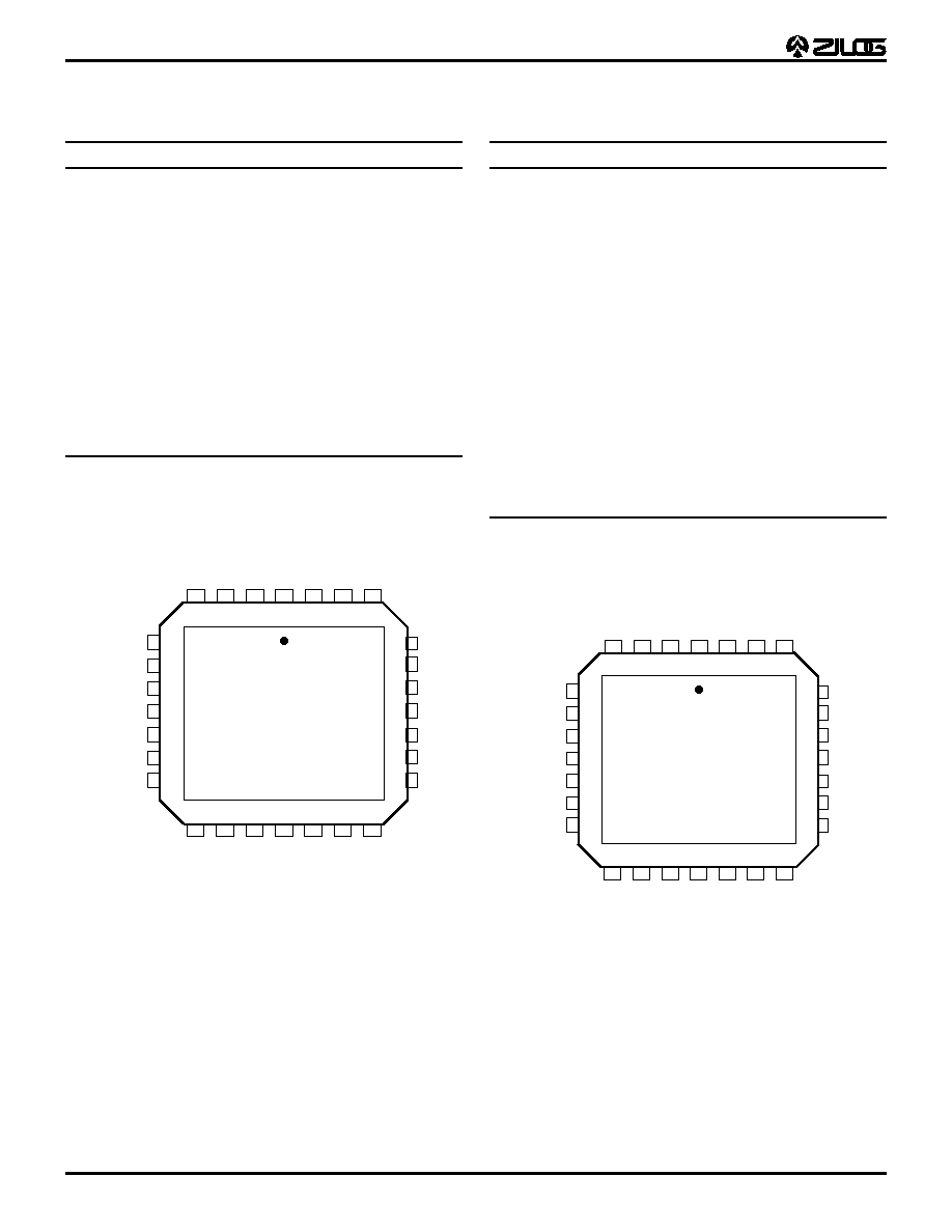
Table 3. Z86C83 28-Pin PLCC Pin Identification
No
Symbol
Function
Direction
1-8
P20-P27
or AC0-AC7
Port 2, Bit 0-7
Analog In 0-7
Input/Output
9
/RESET
Reset
Input
10
XTAL1
Oscillator Clock
Input
11
XTAL2
Oscillator Clock
Output
12
GND
Ground
13
V
CC
Power
14-16
P31-P33
Port 3, Bits 1-3
Input
17
P34
Port 3, Bit 4
Output
18
P36
Port 3, Bit 6
Output
19
P35
Port 3, Bit 5
Output
20-26
P00-P06
Port 0, Bits 0-6
Input/Output
27
A
GND
Analog Ground
28
AV
CC
Analog Power
Figure 4. Z86C83 28-Pin PLCC Pin Configuration
9
5
6
7
8
P27/AC7
P26/AC6
P25/AC5
P24/AC4
/RESET
XTAL1
XTAL2
10
11
1
2
3
4
28
27
26
A
VCC
P23/AC3
P22/AC2
P21/AC1
P20/AC0
AGND
P06
P34
GND
VCC
P31
P32
P33
P36
13
12
18
17
16
14
15
25
24
23
22
21
20
19
P04
P05
P01
P35
P00
P03
P02
Z86C83
PLCC
Table 4. Z86C84 28-Pin PLCC Pin Identification
No
Symbol
Function
Direction
1-8
P20-P27
or AC0-AC7
Port 2, Bit 0-7
Analog In 0-7
Input/Output
9
/RESET
Reset
Input
10
XTAL1
Oscillator Clock
Input
11
XTAL2
Oscillator Clock
Output
12
GND
Ground
13
V
CC
Power
14-16 P31-P33
Port 3, Bits 1-3
Input
17
P34
Port 3, Bit 4
Output
18
P36
Port 3, Bit 6
Output
19
P35
Port 3, Bit 5
Output
20-22 P00-P02
Port 0, Bits 0-3
Input/Output
23
VDLO
D/A Ref. Volt,Low
Input
24
VDHI
D/A Ref. Volt.,High
Input/Output
25-26 DAC2-DAC1 D/A Converter
Output
27
A
GND
Analog Ground
28
AV
CC
Analog Power
Figure 5. Z86C84 28-Pin PLCC Pin Configuration
9
5
6
7
8
P27/AC7
P26/AC6
P25/AC5
P24/AC4
/RESET
XTAL1
XTAL2
10
11
1
2
3
4
28
27
26
A
VCC
P23/AC
3
P22/AC
2
P21/AC1
P20/AC
0
AGND
DAC1
P34
GND
VCC
P31
P32
P33
P36
13
12
18
17
16
14
15
25
24
23
22
21
20
19
VDHI
DAC2
P01
P35
P00
VDLO
P02
Z86C84
PLCC
Z86C83/C84
Z8
Æ
MCU Microcontrollers
DS96DZ80203
5
1
ABSOLUTE MAXIMUM RATINGS
Notice:
Stresses greater than those listed under Absolute
Maximum Ratings may cause permanent damage to the
device. This is a stress rating only; functional operation of
the device at any condition above those indicated in the
operational sections of these specifications is not implied.
Exposure to absolute maximum rating conditions for an
extended period may affect device reliability.
Total power dissipation should not exceed 770 mW for the
package. Power dissipation is calculated as follows:
STANDARD TEST CONDITIONS
The characteristics listed below apply for standard test
conditions as noted. All voltages are referenced to
Ground. Positive current flows into the referenced pin
(Figure 6).
V
DD
SPECIFICATION
V
DD
= 3.0V to 5.5V
Parameter
Min
Max
Units
Ambient Temperature under Bias
≠40
+105
C
Storage Temperature
≠65
+150
C
Voltage on any Pin with Respect to V
SS
[Note 1]
≠0.6
+7
V
Voltage on V
CC
Pin with Respect to V
SS
≠0.3
+7
V
Voltage on /RESET Pins with Respect to V
SS
[Note 2]
≠0.6
V
CC
+1
V
Total Power Dissipation
770
mW
Maximum Current out of V
SS
140
mA
Maximum Current into V
CC
125
mA
Maximum Current into an Input Pin [Note 3]
≠600
+600
µ
A
Maximum Current into an Open-Drain Pin [Note 4]
≠600
+600
µ
A
Maximum Output Current Sinked by Any I/O Pin
25
mA
Maximum Output Current Sourced by Any I/O Pin
25
mA
Notes:
1. This applies to all pins except XTAL and /RESET pins and where otherwise noted.
2. There is no input protection diode from pin to V
CC
.
3. This excludes XTAL pins.
4. Device pin is not at an output Low state.
Total Power Dissipation =
V
CC
x [ I
CC
≠ (sum of I
OH
) ]
+ sum of [ (V
CC
≠ V
OH
) x I
OH
]
+ sum of (V
0L
x I
0L
)
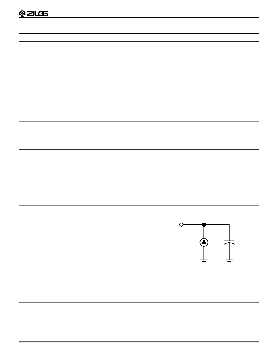
Figure 6. Test Load Diagram
From Output
Under Test
150 pF
I

Z86C83/C84
Z8
Æ
MCU Microcontrollers
6
DS96DZ80203
CAPACITANCE
T
A
= 25
∞
C, V
CC
= GND = 0V, f = 1.0 MHz, unmeasured pins returned to GND.
Parameter
Min
Max
Input capacitance
0
20 pF
Output capacitance
0
20pF
I/O capacitance
0
20 pF
Z86C83/C84
Z8
Æ
MCU Microcontrollers
DS96DZ80203
7
1
DC ELECTRICAL CHARACTERISTICS
Sym Parameter
V
CC
Note 3
T
A
= 0
∞
C
to +70
∞
C
T
A
= ≠40
∞
C
to +105
∞
C
Typical
[13]
@ 25
∞
C Units Conditions
Notes
Min
Max
Min
Max
V
CH
Clock Input High
Voltage
3.0V
0.7 V
CC
V
CC
+0.3
0.7 V
CC
V
CC
+0.3
1.3
V
Driven by External Clock
Generator
5.5V
0.7 V
CC
V
CC
+0.3
0.7 V
CC
V
CC
+0.3
2.5
V
Driven by External Clock
Generator
V
CL
Clock Input Low
Voltage
3.0V
GND-0.3
0.2 V
CC
GND-0.3
0.2 V
CC
0.7
V
Driven by External Clock
Generator
5.5V
GND-0.3
0.2 V
CC
GND-0.3
0.2 V
CC
1.5
V
Driven by External Clock
Generator
V
IH
Input High Voltage
3.0V
0.7 V
CC
V
CC
+0.3
0.7 V
CC
V
CC
+0.3
1.3
V
5.5V
0.7 V
CC
V
CC
+0.3
0.7 V
CC
V
CC
+0.3
2.5
V
V
IL
Input Low Voltage
3.0V
GND-0.3
0.2 V
CC
GND-0.3
0.2 V
CC
0.7
V
5.5V
GND-0.3
0.2 V
CC
GND-0.3
0.2 V
CC
1.5
V
V
OH1
Output High
Voltage
3.0V
V
CC
-0.4
V
CC
-0.4
3.1
V
I
OH
= -2.0 mA
8
5.5V
V
CC
-0.4
V
CC
-0.4
4.8
V
I
OH
= -2.0 mA
8
V
OL1
Output Low
Voltage
3.0V
0.6
0.6
0.2
V
I
OL
= +4.0 mA
8
5.5V
0.4
0.4
0.1
V
I
OL
= +4.0 mA
8
V
OL2
Output Low
Voltage
3.0V
1.2
1.2
0.3
V
I
OL
= +6 mA
8
5.5V
1.2
1.2
0.3
V
I
OL
= +12 mA
8
V
RH
Reset Input High
Voltage
3.0V
.8 V
CC
V
CC
.8 V
CC
V
CC
1.5
V
5.5V
.8 V
CC
V
CC
.8 V
CC
V
CC
2.1
V
V
Rl
Reset Input Low
Voltage
3.0V
GND-0.3
0.2 V
CC
GND-0.3
0.2 V
CC
1.1
V
5.5V
GND-0.3
0.2 V
CC
GND-0.3
0.2 V
CC
1.7
V
V
OFFSET
Comparator Input
Offset
3.0V
25
25
10
mV
10
Voltage
5.5V
25
25
10
mV
10
I
IL
Input Leakage
3.0V
-1
1
-1
2
<1
µ
A
V
IN
= OV, V
CC
5.5V
-1
1
-1
2
<1
µ
A
V
IN
= OV, V
CC
I
OL
Output Leakage
3.0V
-1
1
-1
2
<1
µ
A
V
IN
= OV, V
CC
5.5V
-1
1
-1
2
<1
µ
A
V
IN
= OV, V
CC
I
IR
Reset Input
Current
3.0V
-130
-130
-25
µ
A
5.5V
-180
-180
-40
µ
A
I
CC
Supply Current
3.0V
20
20
7
mA
@ 16 MHz
4, 15
5.5V
25
25
20
mA
@ 16 MHz
4, 15
5.0V
7
7
3
mA
@ 3.58 MHz
4, 15
5.0V
10
10
5
mA
@ 8 MHz
4, 15
I
CC1
Standby Current
3.0V
4.5
4.5
2.0
mA
HALT Mode V
IN
= OV, V
CC
@ 16
MHz
4
5.5V
8
8
3.7
mA
HALT Mode V
IN
= OV, V
CC
@ 16
MHz
4
3.0V
3.4
3.4
1.5
mA
Clock Divide-by-16 @ 16 MHz
4
5.5V
7.0
7.0
2.9
mA
Clock Divide-by-16 @ 16 MHz
4
Z86C83/C84
Z8
Æ
MCU Microcontrollers
8
DS96DZ80203
I
CC2
Standby Current
3.0V
8
15
1
µ
A
STOP Mode V
IN
= OV,
V
CC
WDT is not Running
6,11,15
5.5V
10
20
2
µ
A
STOP Mode V
IN
= OV,
V
CC
WDT is not Running
6,11,15
3.0V
500
600
310
µ
A
STOP Mode V
IN
= OV,
V
CC
WDT is Running
6,11,14,
15
5.5V
800
1000
600
µ
A
STOP Mode V
IN
= OV,
V
CC
WDT is Running
6,11,14,
15
V
ICR
Input Common
Mode
3.0
0
V
CC
-1.0V
0
V
CC
-1.5V
V
10
Voltage Range
5.5
0
V
CC
-1.0V
0
V
CC
-1.5V
V
10
I
ALL
Auto Latch Low
Current
3.0V
8
10
5
µ
A
OV < V
IN
< V
CC
9
5.5V
15
20
11
µ
A
OV < V
IN
< V
CC
9
I
ALH
Auto Latch High
Current
3.0V
-5
-7
-3
µ
A
OV < V
IN
< V
CC
9
5.5V
-8
-10
-6
µ
A
OV < V
IN
< V
CC
9
V
LV
V
CC
Low-Voltage
Protection Voltage
2.0
3.3
2.2
3.6
3.0
V
2
MHz max Int. CLK Freq.
7
Notes:
1. I
CC1
Typical
Max
Unit
Freq
Clock-Driven
0.3 mA
5
mA
8 MHz
2. GND = 0V.
3. 3.0V V
CC
voltage specification guarantees 3.3V
±
0.3V, and 5.5V V
CC
voltage specification guarantees 5.0V
±
0.5V.
4. All outputs unloaded, I/O pins floating, inputs at rail.
5. CL1 = CL2 = 100 pF.
6.
Same as note [4] except inputs at V
CC
.
7. The V
LV
increases as the temperature decreases.
8. Standard Mode (not Low EMI).
9. Auto Latch (mask option) selected.
10. For analog comparator, inputs when analog comparators are enabled.
11. Clock must be forced Low, when XTAL 1 is clock-driven and XTAL2 is floating.
12. Excludes clock pins.
13. Typicals are at V
CC
= 5.0V and 3.3V.
14. Internal RC selected.
15. Combined Digital and Analog V
CC
supply current.
Sym Parameter
V
CC
Note 3
T
A
= 0
∞
C
to +70
∞
C
T
A
= ≠40
∞
C
to +105
∞
C
Typical
[13]
@ 25
∞
C Units Conditions
Notes
Min
Max
Min
Max
Z86C83/C84
Z8
Æ
MCU Microcontrollers
DS96DZ80203
9
1
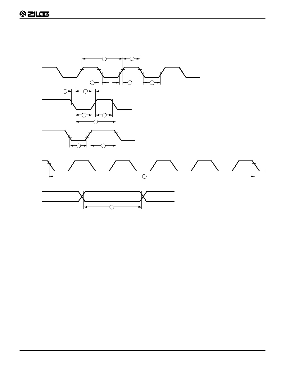
AC ELECTRICAL CHARACTERISTICS
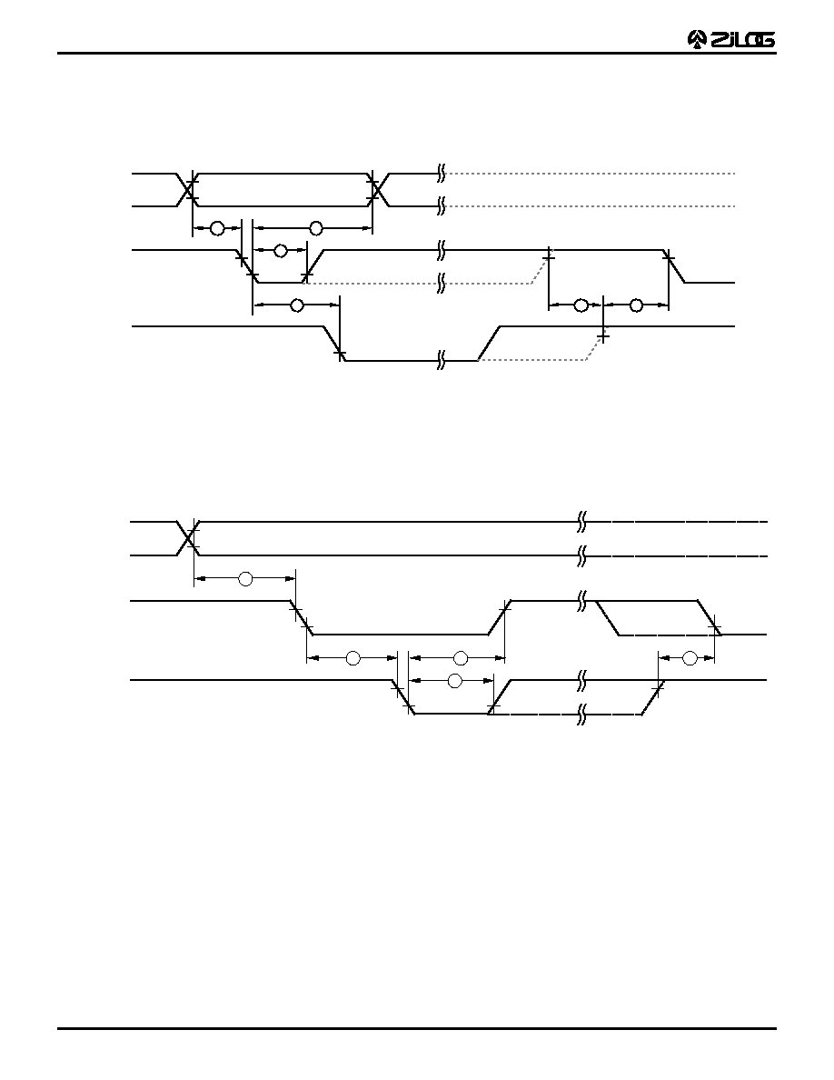
Additional Timing Diagram
Figure 7. Additional Timing
Clock
1
3
4
8
2
2
3
TIN
IRQN
6
5
7
7
11
Clock
Setup
10
9
Stop-Mode
Recovery
Source
Z86C83/C84
Z8
Æ
MCU Microcontrollers
10
DS96DZ80203
AC ELECTRICAL CHARACTERISTICS (Continued)
Additional Timing Table (SCLK/TCLK = XTAL/2)
No Symbol
Parameter
V
CC
Note 6
T
A
= 0
∞
C to +70
∞
C
T
A
= ≠40
∞
C to +105
∞
C
Units Notes
12 MHz
16 MHz
12 MHz
16 MHz
Min
Max
Min
Max
Min
Max
Min
Max
1
TpC
Input Clock Period
3.0V
83
DC
62.5
DC
83
DC
62.5
DC
ns
1
5.5V
83
DC
62.5
DC
83
DC
62.5
DC
ns
1
2
TrC,TfC
Clock Input Rise & Fall
Times
3.0V
15
15
15
15
ns
1
5.5V
15
15
15
15
ns
1
3
TwC
Input Clock Width
3.0V
41
31
41
31
ns
1
5.5V
41
31
41
31
ns
1
4
TwTinL
Timer Input Low Width
3.0V
100
100
100
100
ns
1
5.5V
70
70
70
70
ns
1
5
TwTinH
Timer Input High Width
3.0V
5TpC
5TpC
5TpC
5TpC
1
5.5V
5TpC
5TpC
5TpC
5TpC
1
6
TpTin
Timer Input Period
3.0V
8TpC
8TpC
8TpC
8TpC
1
5.5V
8TpC
8TpC
8TpC
8TpC
1
7
TrTin,
Timer Input Rise & Fall
Timer
3.0V
100
100
100
100
ns
1
TfTin
5.5V
100
100
100
100
ns
1
8A
TwIL
Int. Request Low Time
3.0V
100
100
100
100
ns
1,2
5.5V
70
70
70
70
ns
1,2
8B
TwIL
Int. Request Low Time
3.0V
5TpC
5TpC
5TpC
5TpC
1,3
5.5V
5TpC
5TpC
5TpC
5TpC
1,3
9
TwIH
Int. Request Input High
Time
3.0V
5TpC
5TpC
5TpC
5TpC
1,2
5.5V
5TpC
5TpC
5TpC
5TpC
1,2
10
Twsm
STOP-Mode Recovery
Width Spec
3.0V
12
12
12
12
ns
5.5V
12
12
12
12
ns
11
Tost
Oscillator Startup Time
3.0V
5TpC
5TpC
5TpC
5TpC
4
5.5V
5TpC
5TpC
5TpC
5TpC
4
12
Twdt
Watch-Dog Timer Delay
Time
WDTMR
Reg. D1
D0
3.0V
6.25
6.25
6.25
6.25
ms
0
0
3.0V
12.5
12.5
12.5
12.5
ms
0
1
3.0V
25
25
25
25
ms
1
0
3.0V
100
100
100
100
ms
1
1
13
T
POR
Power On Reset Delay
3.0V
7
24
7
25
7
24
7
25
ms
5.5V
3
13
3
14
3
13
3
14
ms
Notes:
1. Timing Reference uses 0.7 V
CC
for a logic 1 and 0.2 V
CC
for a logic 0.
2. Interrupt request via Port 3 (P31-P33).
3. Interrupt request via Port 3 (P30).
4. SMR-D5 = 0.
5. The V
CC
voltage specification of 3.0V guarantees 3.3V
±
0.3V, and the V
CC
voltage specification of 5.5V guarantees 5.0V
±
0.5V.
Z86C83/C84
Z8
Æ
MCU Microcontrollers
11
DS96DZ80203
AC ELECTRICAL CHARACTERISTICS (Continued)
Additional Timing Table (Divide-By-One Mode, SCLK/TCLK = XTAL)
No Symbol Parameter
V
cc
Note 6
T
A
= 0
∞
C to +70
∞
C T
A
= ≠40
∞
C to +105
∞
C
Units Notes
4 MHz
4 MHz
Min
Max
Min
Max
1
TpC
Input Clock Period
3.0V
250
DC
250
DC
ns
1,7,8
5.5V
250
DC 250
DC
ns
1,7,8
2
TrC,TfC
Clock Input Rise & Fall Times
3.0V
25
25
ns
1,7,8
5.5V
25 25
ns
1,7,8
3
TwC
Input Clock Width
3.0V
125
125
ns
1,7,8
5.5V
125
125
ns
1,7,8
4
TwTinL
Timer Input Low Width
3.0V
100
100
ns
1,7,8
5.5V
70 70
ns
1,7,8
5
TwTinH
Timer Input High Width
3.0V
3TpC
3TpC
1,7,8
5.5V
3TpC 3TpC
1,7,8
6
TpTin
Timer Input Period
3.0V
4TpC
4TpC
1,7,8
5.5V
4TpC 4TpC
1,7,8
7
TrTin,
Timer Input Rise & Fall Timer
3.0V
100
100
ns
1,7,8
TfTin
5.5V
100
100
ns
1,7,8
8A TwIL
Int. Request Low Time
3.0V
100
100
ns
1,2,7,8
5.5V
70
70
ns
1,2,7,8
8B TwIL
Int. Request Low Time
3.0V
3TpC
3TpC
1,3,7,8
5.5V
3TpC
3TpC
1,3,7,8
9
TwIH
Int. Request Input High Time
3.0V
3TpC
3TpC
1,2,7,8
5.5V
3TpC
2TpC
1,2,7,8
10 Twsm
STOP-Mode Recovery Width Spec
3.0V
12
12
ns
4,8
5.5V
12 12
ns
4,8
11 Tost
Oscillator Startup Time
3.0V
5TpC
5TpC
4,8,9
5.5V
5TpC 5TpC
4,8,9
Notes:
1. Timing Reference uses 0.7 V
CC
for a logic 1 and 0.2 V
CC
for a logic 0.
2. Interrupt request via Port 3 (P33-P31).
3. Interrupt request via Port 3 (P30).
4. SMR-D5 = 1, POR STOP mode delay is on.
5. Reg. WDTMR.
6. The V
CC
voltage specification of 3.0V guarantees 3.3V
±
0.3V, and the V
CC
voltage specification of 5.5V guarantees 5.0V
±
0.5V.
7. SMR D1 = 0.
8. Maximum frequency for internal system clock is 4 MHz when using XTAL divide-by-one mode.
9. For XTAL and LC oscillator, and for oscillator driven by clock driver.
Z86C83/C84
Z8
Æ
MCU Microcontrollers
12
DS96DZ80203
AC ELECTRICAL CHARACTERISTICS
Handshake Timing Diagrams
Figure 8. Input Handshake Timing
Figure 9. Output Handshake Timing
Data In
1
2
3
4
5
6
/DAV
(Input)
RDY
(Output)
Next Data In Valid
Delayed RDY
Delayed DAV
Data In Valid
Data Out
/DAV
(Output)
RDY
(Input)
Next Data Out Valid
Delayed RDY
Delayed DAV
Data Out Valid
7
8
9
10
11
Z86C83/C84
Z8
Æ
MCU Microcontrollers
13
DS96DZ80203
AC ELECTRICAL CHARACTERISTICS (Continued)
Handshake Timing Table
No
Symbol
Parameter
V
CC
Note1,2
T
A
= 0
∞
C to +70
∞
C
T
A
= ≠40
∞
C to +105
∞
C
Data
Direction
12 MHz
16 MHz
12 MHz
16 MHz
Min Max Min Max Min Max Min Max
1
TsDI(DAV)
Data In Setup Time
3.0V
0
0
0
0
IN
5.5V
0
0
0
0
IN
2
ThDI(DAV)
Data In Hold Time
3.0V
160
160
160
160
IN
5.5V
115
115
115
115
IN
3
TwDAV
Data Available Width
3.0V
155
155
155
155
IN
5.5V
110
110
110
110
IN
4
TdDAVI(RDY)
DAV Fall to RDY Fall Delay
3.0V
160
160
160
160
IN
5.5V
115
115
115
115
IN
5
TdDAVId(RDY)
DAV Rise to RDY Rise Delay
3.0V
120
120
120
120
IN
5.5V
80
80
80
80
IN
6
TdRDY0(DAV)
RDY Rise to DAV Fall Delay
3.0V
0
0
0
0
IN
5.5V
0
0
0
0
IN
7
TdD0(DAV)
Data Out to DAV Fall Delay
3.0V
42
31
42
31
OUT
5.5V
42
31
42
31
OUT
8
TdDAV0(RDY)
DAV Fall to RDY Fall Delay
3.0V
0
0
0
0
OUT
5.5V
0
0
0
0
OUT
9
TdRDY0(DAV)
RDY Fall to DAV Rise Delay
3.0V
160
160
160
160
OUT
5.5V
115
115
115
115
OUT
10 TwRDY
RDY Width
3.0V
110
110
110
110
OUT
5.5V
80
80
80
80
OUT
11 TdRDY0d(DAV) RDY Rise to DAV Fall Delay
3.0V
110
110
110
110
OUT
5.5V
80
80
80
80
OUT
Notes:
1. Timing Reference uses 0.7 V
CC
for a logic 1 and 0.2 V
CC
for a logic 0.
2. The V
CC
voltage specification of 3.0V guarantees 3.3V
±
0.3V and the V
CC
voltage specification of 5.5V guarantees 5.0V
±
0.5V.

Z86C83/C84
Z8
Æ
MCU Microcontrollers
14
DS96DZ80203
Table 5. D/A Converter Electrical Characteristics
V
CC
= 3.3V
±
10%
Parameter
Minimum
Typical
Maximum
Units
Resolution
8
Bits
Integral non-linearity
0.25
1
LSB
Differential non-linearity
0.25
0.5
LSB
Setting time, 1/2 LSB
1.5
3.0
µ
sec
Zero Error at 25
∞
C
10
20
mV
Full Scale error at 25
∞
C
0.25
0.5
LSB
Supply Range
3.0
3.3
3.6
Volts
Power dissipation, no load
10
mW
Ref Input resistance
2K
4K
10K
Ohms
Output noise voltage
50
µ
Vp-p
VDHI
range at 3 volts
1.5
1.8
2.1
Volts
VDLO range at 3 volts
0.2
0.5
0.8
Volts
VDHI≠VDLO, at 3 volts
1.3
1.6
1.9
Volts
Capacitive output load, CL
20
pF
Resistive output load, RL
50K
Ohms
Output slew rate
1.0
3.0
V/
µ
sec
Notes:
Voltage: 3.0V to 3.6V
Temp: 0≠70
∞
C
Table 6. D/A Converter Electrical Characteristics
V
CC
= 5.0V
±
10%
Parameter
Minimum
Typical
Maximum
Units
Resolution
8
Bits
Integral non-linearity
0.25
1
LSB
Differential non-linearity
0.25
0.5
LSB
Setting time, 1/2 LSB
1.5
3.0
µ
sec
Zero Error at 25
∞
C
10
20
mV
Full Scale error at 25
∞
C
1
2
% FSR
Supply Range
4.5
5.0
5.5
Volts
Power dissipation, no load
50
85
mW
Ref Input resistance
2K
4K
10K
Ohms
Output noise voltage
50
µ
Vp-p
VDHI
range at 5 volts
2.6
3.5
Volts
VDLO range at 5V volts
0.8
1.7
Volts
VDHI≠VDLO, at 5V volts
0.9
2.7
Volts
Capacitive output load, CL
30
pF
Resistive output load, RL
20K
Ohms
Output slew rate
1.0
3.0
V/
µ
sec
Notes:
Voltage: 4.5V - 5.5V
Temp: 0-70
∞
C
The C84 Emulator has maximum setting time of 20
µ
sec. (10
µ
sec. typical).

Z86C83/C84
Z8
Æ
MCU Microcontrollers
15
DS96DZ80203
AC ELECTRICAL CHARACTERISTICS (Continued)
Table 7. A/D Converter Electrical Characteristics
V
CC
= 3.3V
±
10%
Parameter
Minimum
Typical
Maximum
Units
Resolution
8
Bits
Integral non-linearity
0.5
1
LSB
Differential non-linearity
0.5
1
LSB
Zero Error at 25
∞
C
5.0
mV
Supply Range
3.0
3.3
3.6
Volts
Power dissipation, no load
20
40
mW
Clock frequency
24
MHz
Input voltage range
VA
LO
VA
HI
Volts
Conversion time
4.3
35 X SCLK
µ
sec
Input capacitance on ANA
25
40
pF
VA
HI
range
VA
LO
+2.5
AV
CC
Volts
VA
LO
range
AN
GND
AV
CC
≠2.5
Volts
VA
HI
-≠VA
LO
2.5
AV
CC
Volts
Notes:
Voltage: 3.0V to 3.6V
Temp: 0-70
∞
C
SCLK = System Clock on Bus Speed.
Table 8. A/D Converter Electrical Characteristics
V
CC
= 5.0V
±
10%
Parameter
Minimum
Typical
Maximum
Units
Resolution
8
Bits
Integral non-linearity
0.5
1
LSB
Differential non-linearity
0.5
1
LSB
Zero Error at 25
∞
C
45
mV
Supply Range
4.5
5.0
5.5
Volts
Power dissipation, no load
50
85
mW
Clock frequency
33
MHz
Input voltage range
VA
LO
VA
HI
Volts
Conversion time
4.3
35 X SCLK
µ
sec
Input capacitance on ANA
25
40
pF
VA
HI
range
VA
LO
+2.5
AV
CC
Volts
VA
LO
range
AN
GND
AV
CC
≠2.5
Volts
VA
HI
-≠VA
LO
2.5
AV
CC
Volts
Notes:
Voltage: 4.5V ≠5.5V
Temp: 0-70
∞
C
Conversion time is defined as the time from initiation of A-D conversion to storage of the digital result in the ADR register.
SCLK = System Clock on Bus Speed.

Z86C83/C84
Z8
Æ
MCU Microcontrollers
16
DS96DZ80203
PIN FUNCTIONS
Application Precaution
The production test-mode environment may be enabled
accidentally during normal operation if
excessive noise
surges above V
cc
occur on the /RESET pin.
Recommendations for dampening voltage surges in both
test and OTP mode include the following:
s
Using a clamping diode to /RESET
s
Adding a capacitor to the affected pin
XTAL1.
Crystal 1 (time-based input). This pin connects a
parallel-resonant crystal, ceramic resonator, LC network
or an external single-phase clock to the on-chip oscillator
input.
XTAL2.
Crystal 2 (time-based output). This pin connects a
parallel-resonant crystal, ceramic resonator, LC network to
the on-chip oscillator output.
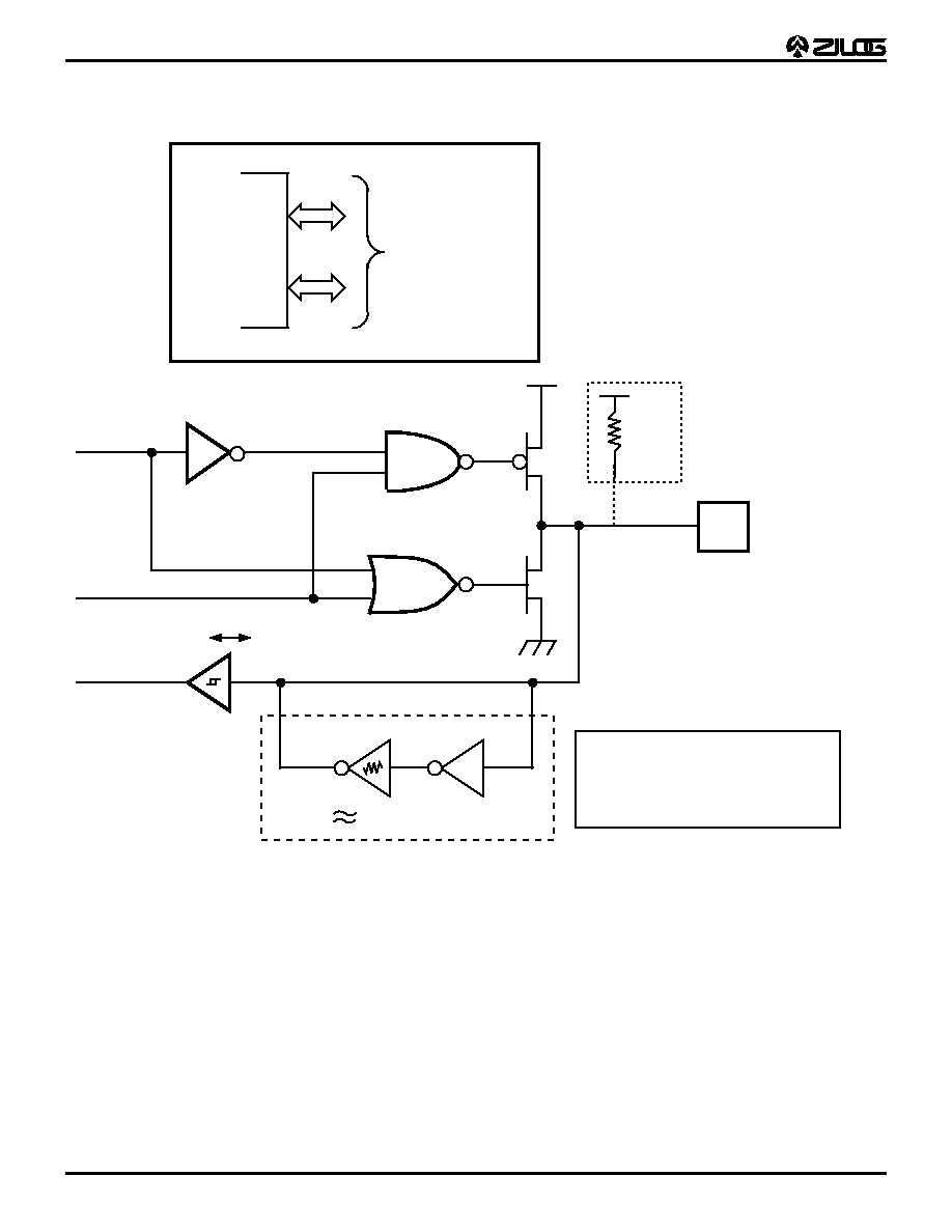
Port 0 P00-P06.
(P03-P06 is not available on the
Z86C84).
Port 0 is a 7-bit, bidirectional, CMOS-compatible
I/O port. These seven I/O lines can be nibble
programmable as P00-P03 input/output and P04-P06
input/output, separately (Figure 10). All input buffers are
Schmitt-triggered and output drivers are push-pull. There
is a ROM mask option to enable 100K (
±
40%) pull-up
resistors to Port 0, P00 to P02.
Port 0 Auto Latch.
(Auto Latch Mask Option available
only on P00-P02. P03-P06 has the Auto Latches
permanently enabled.) The Auto Latch provides valid
CMOS Levels when P00-P06 (P00-P02 on C84) are
selected as inputs and not externally driven. It is
impossible to determine if a non-driven input is 1 or 0,
however; the Auto Latch will sense the input condition and
drive a valid CMOS level, thereby eliminating a floating
mode that could cause excessive current. (Auto Latch is a
ROM mask option for the Z86C83, Z86C84).
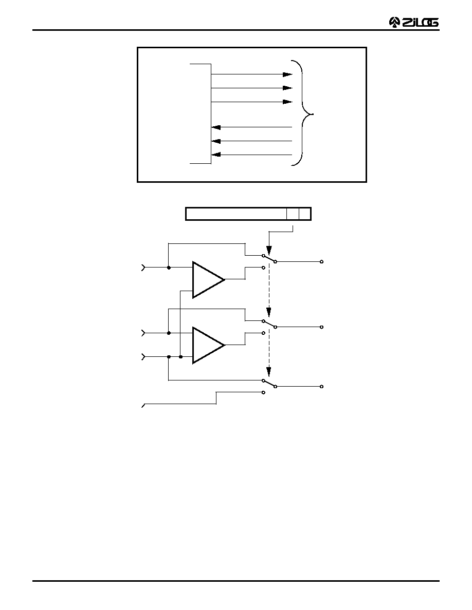
Port 2 (P27-P20) Port 2 is an 8-bit, bi-directional, CMOS-
compatible I/O port and an 8-channel muxed input to the
8-bit ADC. When configured as a digital input, by
programming the Port2 Mode register, the Port 2 register
can be evaluated to read digital data applied to Port 2, or
the ADC result register can be read to evaluate the analog
signals applied to Port 2 after configuring the ADC Control
Registers. The direction of each of the eight Port 2 I/O lines
can be configured individually (Figure 11).
In addition, all four versions of the device provide the
capability of connecting 10K (
±
20%) pull-up resistors to
each of the Port 2 I/O lines individually. The pull-ups are
connected when activated through software control of
P2RES register (Figure 67) when the corresponding Port
2 pin is configured to be an input. The pull-up resistor of a
Port 2 I/O line is automatically disabled when the
corresponding I/O is an output, regardless of the state of
the corresponding P2RES bit value.
Note: The Z86C83/C84 Emulator does not emulate the
P2RES Register. Selection of the pull-ups are done via
jumper settings on the emulator.
Z86C83/C84
Z8
Æ
MCU Microcontrollers
17
DS96DZ80203
PIN FUNCTIONS (Continued)
Figure 10. Port 0 Configuration
R 500 k
/OEN
Out
In
1.5 2.3 Hysteresis
Pad
100K
ROM Mask Pull-Up Option
(P00-P02 only)
Port 0 (I/O)
Notes:
Auto Latch
C83/E83: P00-P02 Mask Option
P03-P06 Permanent
C84/E84: P00 - P02 Mask Option
Z86C83/C84
Z8
Æ
MCU Microcontrollers
18
DS96DZ80203
Figure 11. Port 2 Configuration
Port 2 (I/O)
/C83
/C84
/E84
P27
P26
P25
P24
P23
P22
P21
P20
P2
Analog Mux
Select from
P2RES
ADC0 (Bits 7, 6, 5)
Input_en
/OEN
Data
ADC
10K
Pad

Z86C83/C84
Z8
Æ
MCU Microcontrollers
19
DS96DZ80203
PIN FUNCTIONS (Continued)
Port 3 (P37-P30). Port 3 is a 6-bit, CMOS-compatible
port, with three fixed inputs (P33-P31) and three fixed
outputs (P34-P36), configured under software control for
Input/Output, Counter/Timers, interrupt, and port
handshake. P31, P32, and P33 are standard CMOS inputs
(no Auto Latches). Pins P34, P35, and P36 are push-pull
output lines (Figure 11). Low EMI output buffers can be
globally programmed by the software.
Two on-board comparators can process analog signals on
P31 and P32 with reference to the voltage on P33. The
analog function is enabled by programming Port 3 Mode
Register (P3M bit 1). For Interrupt functions, Port 3, pin 3
is falling-edge interrupt input. P31 and P32 are
programmable as rising, falling, or both edge triggered
interrupts (IRQ register bits 6 and bit 7). P33 is the
comparator reference voltage input when in Analog Mode.
Access to Counter/Timers 1 is made through P31 (T
IN
) and
P36 (T
OUT
). Handshake lines for Ports 0 and 2 are available
on P31/P36 and P32/P35 (Table 9).
Port 3 also provides the following control functions:
handshake for Ports 0 and 2 (/DAV and RDY); three
external interrupt request signals (IRQ2-IRQ0); timer input
and output signals (T
IN
and T
OUT
).
Auto Latch. The Auto-Latch instruction puts valid CMOS
levels on all CMOS inputs (except P33-P31) that are not
externally driven. Whether this level is 0 or 1, cannot be
determined. A valid CMOS level, rather than a floating
node, reduces excessive supply current flow in the input
buffer.
Notes:
1.
Deletion of Port Auto Latches is available as a ROM
mask option. The Auto Latch Delete option is selected
by the customer when the ROM code is submitted.
2.
Ports 03, 04, 05, 07 have permanently enabled Auto
Latches.
Comparator Inputs. Port 3, P31 and P32, each have a
comparator front end. The comparator reference voltage,
P33, is common to both comparators. In analog mode, the
P33 input functions as a reference voltage to the
comparators. In Analog Mode, the internal P33 register
and its corresponding IRQ1 is connected to the Stop-Mode
Recovery source selected by the SMR register. In this
mode, any of the Stop-Mode Recovery sources are used
to toggle the P33 bit or generate IRQ1. In Digital Mode,
P33 can be used as a Port 3 register input or IRQ1 source.
P34 outputs the comparator outputs by software
programming the PCON Register bit D0 to 1.
Table 9. Port 3 Pin Assignments
Pin
I/O
CTC1
Analog
Int.
P0 HS P2 HS
P31 IN
T
IN
AN1
IRQ2
D/R
P32 IN
AN2
IRQ0 D/R
P33 IN
REF
IRQ1
P34 OUT
AN1-OUT
P35 OUT
R/D
P36 OUT
T
OUT
R/D
Notes:
HS = Handshake Signals
D = /DAV
R = RDY
Z86C83/C84
Z8
Æ
MCU Microcontrollers
20
DS96DZ80203
Figure 12. Port 3 Input Configuration
Port 3 (I/O)
Port 3
Z86C83/C84
P36
P35
P34
P33
P32
P31
D1
R247 = P3M
P31 (AN1)
P32 (AN2)
P33 (REF)
From Stop-Mode Recovery
Source
1 = Analog
0 = Digital
IRQ2, T
IN
, P31 Data Latch
IRQ0, P32 Data Latch
IRQ1, P33 Data Latch
DIG.
AN
+
-
+
-
Z86C83/C84
Z8
Æ
MCU Microcontrollers
21
DS96DZ80203
PIN FUNCTIONS (Continued)
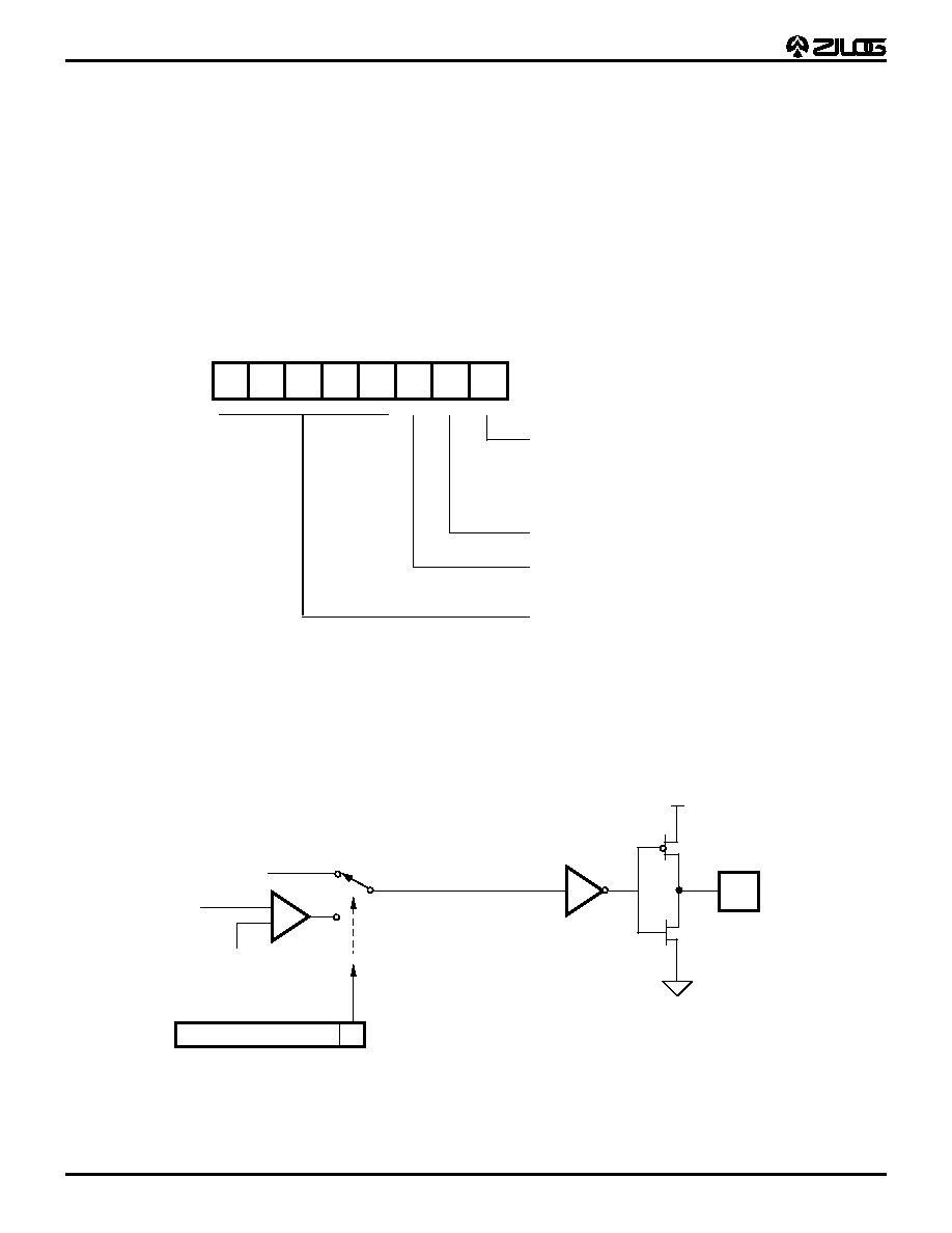
Port Configuration Register (PCON). The PCON con-
figures the ports individually for comparator output on Port
3. The PCON Register is located in the Expanded Register
File at Bank F, location 00 (Figure 13).
Bit 0 multiplexes comparator AN1 Output at P34. A "1" in
this location brings the comparator output to P34
(Figure 14), and a "0" puts P34 into its standard I/O
configuration.
Note: Only comparator output AN1 is multiplexed to a
Port 3 output. Comparator AN2 output is not connected to
any pins. Note that the PCON Register is reset upon the
occurrence of a WDT RESET (not in Stop Mode), and
Power-On Reset (POR).
Figure 13. Port Configuration Register (PCON) (Write-Only)
Figure 14. Port 3 P34 Output Configuration
D7
D6
D5
D4
D3
D2
D1
D0
Comparator
Output Port 3
0 P34 Standard Output
*
1 P34 Comparator Output
Reserved (Must be 1.)
PCON (F) 00
* Default setting from Stop-Mode Recovery,
Power-On Reset, and any WDT Reset.
0 Port 0 Open-Drain
1 Port 0 Push-Pull*
Reserved (Must be 1.)
P34 OUT
P31
+
-
REF (P33)
P34
PAD
PCON
D0
*
Reset Condition
Normal
0 P34 Standard Output
1 P34 Comparator Output
*
AN1
Z86C83/C84
Z8
Æ
MCU Microcontrollers
22
DS96DZ80203
FUNCTIONAL DESCRIPTION
RESET.
(Input, Active Low). This pin initializes the MCU.
Reset is accomplished either through Power-On Reset
(POR), Watch-Dog Timer (WDT) Reset, or external reset.
During POR, and WDT Reset, the internally generated
reset is driving the reset pin Low for the POR time.
Any
devices driving the reset line must be open-drain to
avoid damage from a possible conflict during reset
conditions. Pull-up is provided internally.
After the POR time, /RESET is a Schmitt-triggered input.
After the reset is detected, an internal RST signal is
latched and held for an internal register count of 18
external clocks, or for the duration of the external reset,
whichever is longer. Program execution begins at location
000C (hex), 5-10 TpC cycles after the RST is released. For
POR, the reset output time is T
POR
.
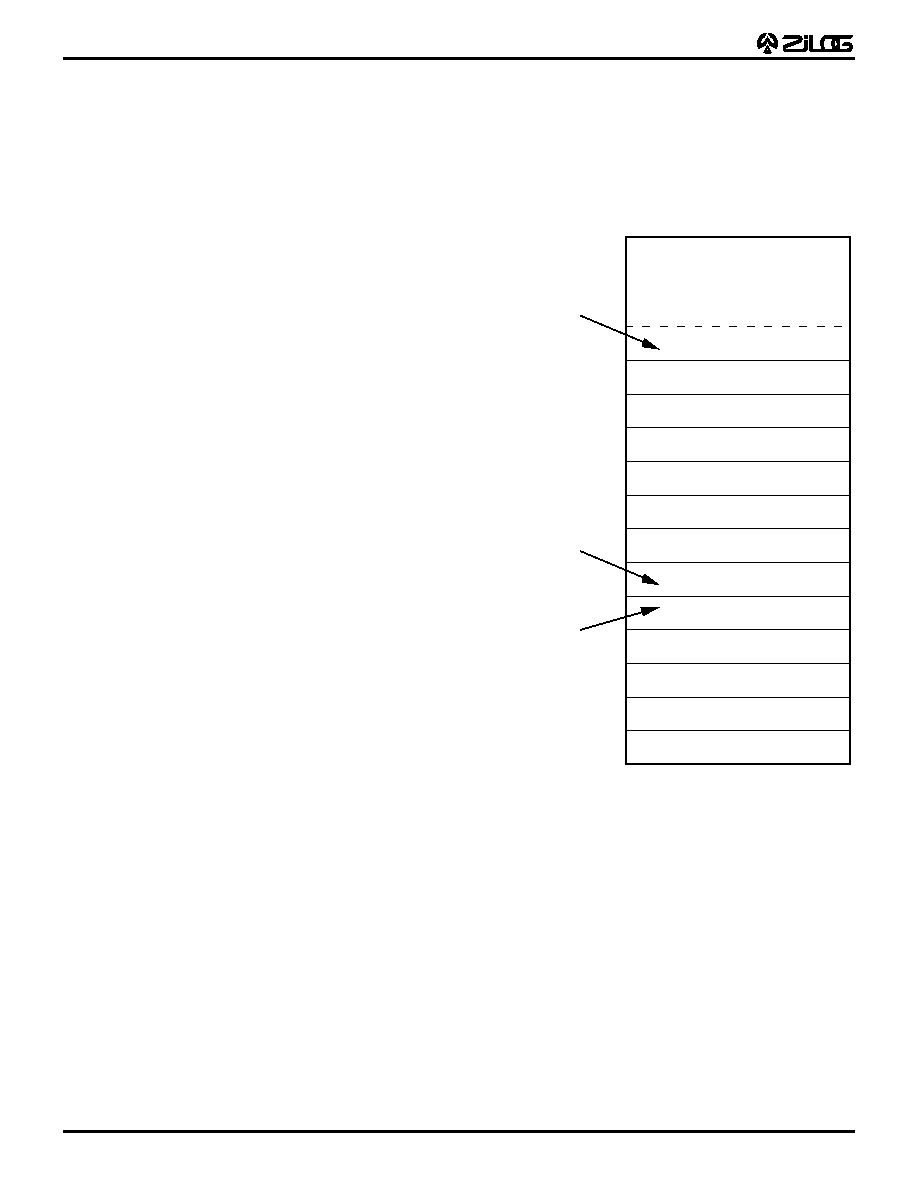
Program Memory. C83/C84 can address up to 4 KB of
internal Program Memory (Figure 15). The first 12 bytes of
program memory are reserved for the interrupt vectors.
These locations contain six 16-bit vectors that correspond
to the six available interrupts. Bytes 13 to 4095 consist of
on-chip, mask-programmed ROM.
ROM Protect. The 4 KB of Program Memory is mask
programmable. A ROM protect feature will prevent
dumping of the ROM contents from an external program
outside the ROM.
Expanded Register File. The register file has been
expanded to allow for additional system control registers
and for mapping of additional peripheral devices and
input/output ports into the register address area. The Z8
register address space R0 through R15 is implemented as
16 groups of 16 registers per group (Figure 16). These
register banks are known as the Expanded Register File
(ERF). Bits 3-0 of the Register Pointer (RP) select the
active ERF bank. Bits 7-4 of register RP select the working
register group (Figure 17). Four system configuration
registers reside in the ERF address space in Bank F and
eight registers reside in Bank C. The rest of the ERF
addressing space is not physically implemented, and is
open for future expansion.
Note: When using Zilog's Cross Assembler version 2.1 or
earlier, use the LD RP, #0X instruction rather than the SRP
#0X instruction to access the ERF.
Figure 15. Program Memory Map
12
11
10
9
8
7
6
5
4
3
2
1
0
On-Chip
ROM
Location of
First Byte of
Instruction
Executed
After RESET
Interrupt
Vector
(Lower Byte)
Interrupt
Vector
(Upper Byte)
IRQ5
IRQ4
IRQ4
IRQ3
IRQ3
IRQ2
IRQ2
IRQ1
IRQ1
IRQ0
IRQ0
IRQ5
2048/4096
Z86C83/C84
Z8
Æ
MCU Microcontrollers
23
DS96DZ80203
FUNCTIONAL DESCRIPTION (Continued)
\
Figure 16. Expanded Register File Architecture
U = Unkno
wn
*
Will not be reset with a Stop--Mode Reco
v
e
r
y
**
All addresses are in He
xadecimal
Will not be reset with a Stop-Mode Reco
v
e
r
y
, e
xcept Bit 0.
Notes:
7
654321
0
W
o
r
king Register
Group P
ointer
Expanded Register
Group P
ointer
FF
FO
7F
0F
00
Z8 Register File**
REGISTER POINTER
(F) 0F
(F) 0E
(F) 0D
(F) 0C
(F) 0B
(F) 0A
(F) 09
(F) 08
(F) 07
(F) 06
(F) 05
(F) 04
(F) 03
(F) 02
(F) 01
(F) 00
WDTMR
SMR
UU
U
0
1
101
00
100
0
0
0
REGISTER**
EXP
ANDED REG.
GR
OUP
(F)
RESET CONDITION
Z8
Æ
ST
AND
ARD CONTR
OL
REGISTERS
Reser
v
e
d
*
Reser
v
e
d
SMR2
Reser
v
e
d
Reser
v
e
d
Reser
v
e
d
Reser
v
e
d
Reser
v
e
d
Reser
v
e
d
Reser
v
e
d
Reser
v
e
d
Reser
v
e
d
Reser
v
e
d
Reser
v
e
d
PCON
1
1
*
U1
1
1
U
U
UU
UU
UU
U
UUU
UU
UU
UU
U
U
U
U
U
UU
U
UU
REGISTER**
EXP
ANDED REG.
GR
OUP
(0)
RESET CONDITION
(0) 03
P3
(0) 02
P2
(0) 01
P1
(0) 00
P0
*
*
U
U
UUU
U
0
0
Reser
v
e
d
1
1
1
1
1
1
0
0
0
U
0
0
U
0
0
1
0
0
0
U
U
0
U
1
0
1
0
0
0
U
U
0
U
0
0
1
0
0
0
U
U
0
U
0
0
1
0
0
0
U
U
0
U
1
0
1
0
0
0
U
U
0
U
1
0
1
0
0
0
U
U
0
U
0
0
1
0
0
0
U
U
0
U
1
0
1
RESET CONDITION
D7
D6
D5
D4
D3
D2
D1
D0
UU
U
U
U
UU
U
UU
U
UUU
U
U
UU
U
UU
U
UU
UU
U
U
U
UU
U
0
0
00
0
000
0U
U
00
00
0
FF
FE
FD
FC
FB
FA
F9
F8
F7
F6
F5
F4
F3
F2
F1
F0
SPL
RP
FLA
GS
IMR
IRQ
IPR
P01M
P3M
P2M
REGISTER**
*
*
P0
T0
P1
T1
TMR
Reser
v
e
d
EXP
ANDED REG.
GR
OUP
(C)
REGISTER
(C) 0F
(C) 0E
(C) 0D
(C) 0C
(C) 0B
(C) 0A
(C) 09
(C) 08
(C) 07
(C) 06
(C) 05
Reserved
Reserved
Reserved
Reserved
ADR1
ADC1
ADC0
DAC2
DAC1
DACR2
RESET CONDITION
U
UU
U
U
U
U
UUU
U
U
U
U
U
0
1
U
0
UUU
UU
U
U
U
U
1
U
0
UU
UUU
U
U
U
U
1
U
0
U
U
U
0
U
0
0UU
U
UUU
U
U
U
U
0
UU
UU
U
UU
U
000
0
0
00
0U
U
U
0
(C) 04
(C) 03
DACR1
P2RES
(C) 02
Reserved
(C) 01
(C) 00
Reserved
Reserved
U
U
U
U
UUU0
U
U
U
U
UUU
U
U
U
U
U
U
U
UU
U
U
U
U
U
U
U
UUU
UU
U
U
U
U
Reserved
00
0
0000
*
GPR
*
*
*
*
*
*
*
Z86C83/C84
Z8
Æ
MCU Microcontrollers
24
DS96DZ80203
Register File. The Register File consists of three I/O port
registers, 237 general-purpose registers, 15 control and
status registers, and four system configuration registers in
the Expanded Register Group (Figure
16). The
instructions can access registers directly or indirectly
through an 8-bit address field. This allows a short 4-bit
register address using the Register Pointer (Figure 18). In
the 4-bit mode, the Register File is divided into 16 working
register groups, each occupying 16 continuous locations.
The Register Pointer addresses the starting location of the
active working-register group.
Note: Register Bank E0-EF is only accessed through
working registers and indirect addressing modes.
CAUTION: D4 of Control Register P01M (R251) must
be 0.
R254. The C83/C84 has one extra general-purpose
register located at FEH (R254). It is set to 00H after any
reset.
Stack. The C83/C84 has an 8-bit Stack Pointer (R255)
used for the internal stack that resides within the 236
general-purpose registers. Register R254 cannot be used
for stack.
General-Purpose Registers (GPR). These registers are
undefined after the device is powered up. The registers
keep their last value after any reset, as long as the reset
occurs in the V
CC
voltage-specified operating range. It will
not keep its last state from a V
LV
reset if the V
CC
drops below
1.8V. This includes Register R254.
Note: Register Bank E0-EF is only accessed through
working register and indirect addressing modes.
RAM Protect. The upper portion of the RAM's address
spaces %80F to %EF (excluding the control registers) are
protected from reading and writing. The RAM Protect bit
option is mask-programmable and is selected by the
customer when the ROM code is submitted. After the mask
option is selected, the user activates this feature from the
internal ROM code to turn off/on the RAM Protect by
loading either a 0 or 1 into the Interrupt Mask (IMR)
register, bit D6. A 1 in D6 enables RAM Protect.
Figure 17. Register Pointer Register
D7
D6
D5
D4
D3
D2
D1
D0
Expanded Register Group
Working Register Group
RP
R253
Note: Default Setting After Reset = 00000000
Figure 18. Register Pointer
The upper nibble of the register file address
provided by the register pointer specifies
the active working-register group.
r7
r6
r5
r4
R253
(Register Pointer)
I/O Ports*
Specified Working
Register Group
The lower nibble
of the register
file address
provided by the
instruction points
to the specified
register.
r3
r2
r1
r0
Register Group 1
Register Group 0*
R15 to R0
R15 to R4*
R3 to R0*
R15 to R0
FF
F0
0F
00
1F
10
2F
20
3F
30
4F
40
5F
50
6F
60
7F
70
* Expanded Register File Bank (0) is selected
in this figure by handling bits D3 to D0 as "0"
in Register R253 (RP).
Z86C83/C84
Z8
Æ
MCU Microcontrollers
25
DS96DZ80203
FUNCTIONAL DESCRIPTION (Continued)
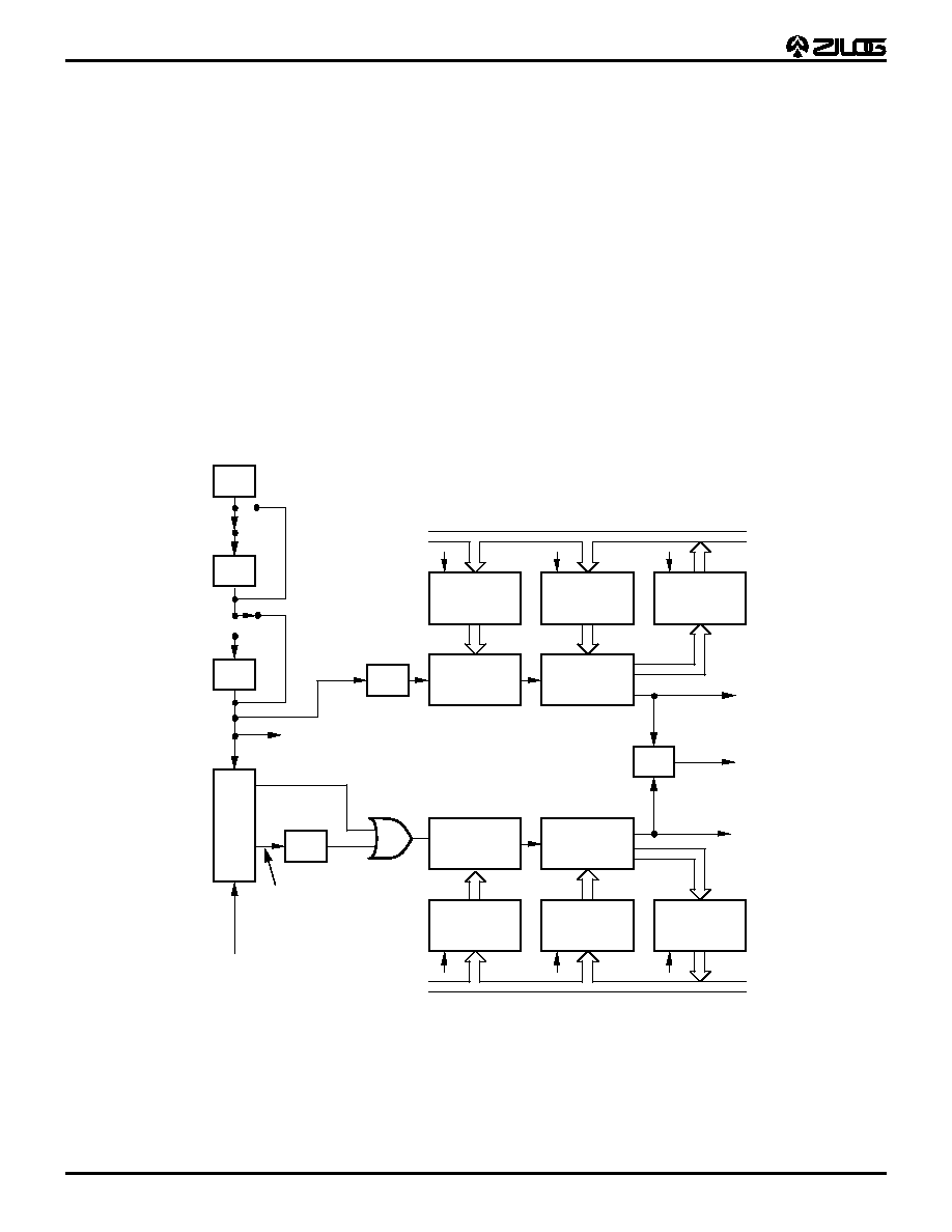
Counter/Timers. There are two 8-bit programmable
counter/timers (T0-T1), each driven by its own 6-bit
programmable prescaler. The T1 prescaler is driven by
internal or external clock sources; however, the T0
prescaler is driven by the internal clock only (Figure 19).
The 6-bit prescalers can divide the input frequency of the
clock source by any integer number from 1 to 64. Each
prescaler drives its counter, which decrements the value
(1 to 256) that has been loaded into the counter. When the
counter reaches the end of the count, a timer interrupt
request, IRQ4 (T0) or IRQ5 (T1), is generated.
The counters can be programmed to start, stop, restart to
continue, or restart from the initial value. The counters can
also be programmed to stop upon reaching zero (single
pass mode) or to automatically reload the initial value and
continue counting (modulo-n continuous mode).
The counters,
but not the prescalers, are read at any
time without disturbing their value or count mode. The
clock source for T1 is user-definable and is either the
internal microprocessor clock divide-by-four, or an
external signal input through Port 3. The Timer Mode
register configures the external timer input (P31) as an
external clock, a trigger input that can be retriggerable or
non-retriggerable, or as a gate input for the internal clock.
The counter/timers can be cascaded by connecting the T0
output to the input of T1. T
IN
Mode is enabled by setting
R243 PRE1 Bit D1 to 0.
Figure 19. Counter/Timer Block Diagram
PRE0
Initial Value
Register
T0
Initial Value
Register
T0
Current Value
Register
6-Bit
Down
Counter
8-bit
Down
Counter
˜
16
˜
4
6-Bit
Down
Counter
8-Bit
Down
Counter
PRE1
Initial Value
Register
T1
Initial Value
Register
T1
Current Value
Register
˜
2
Clock
Logic
IRQ4
TOUT
P36
IRQ5
Internal Data Bus
Write
Write
Read
Internal Clock
Gated Clock
Triggered Clock
TIN P31
Write
Write
Read
Internal Data Bus
External Clock
Internal
Clock
D0 (SMR)
˜
4
˜
2
OSC
D1 (SMR)
Z86C83/C84
Z8
Æ
MCU Microcontrollers
26
DS96DZ80203
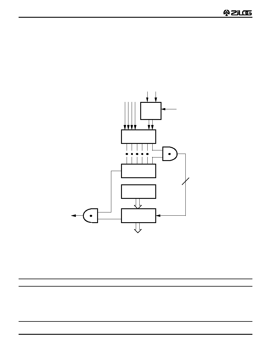
Interrupts. The Z8 has six different interrupts from six
different sources. These interrupts are maskable,
prioritized (Figure 20) and the six sources are divided as
follows: four sources are claimed by Port 3 lines P33-P30,
and two in counter/timers (Table 10). The Interrupt Mask
Register globally or individually enables or disables the six
interrupt requests.
When more than one interrupt is pending, priorities are
resolved by a programmable priority encoder that is
controlled by the Interrupt Priority register. An interrupt
machine cycle is activated when an interrupt request is
granted. This action disables all subsequent interrupts,
saves the Program Counter and Status Flags, and then
branches to the program memory vector location reserved
for that interrupt.
Figure 20. Interrupt Block Diagram
Table 10. Interrupt Types, Sources, and Vectors
Name
Source
Vector Location
Comments
IRQ0
/DAV0, IRQ0
0, 1
External (P32), Rise/ Fall Edge Triggered
IRQ1,
IRQ1
2, 3
External (P33), Fall Edge Triggered
IRQ2
/DAV2, IRQ2, T
IN
4, 5
External (P31), Rise /Fall Edge Triggered
IRQ3
IRQ3
6, 7
By User Software
IRQ4
T0
8, 9
Internal
IRQ5
T1
10, 11
Internal
Interrupt
Edge
Select
IRQ (D6, D7)
IRQ1, 3, 4, 5
IRQ
IMR
IPR
PRIORITY
LOGIC
6
Global
Interrupt
Enable
Vector Select
Interrupt
Request
IRQ0 IRQ2
Z86C83/C84
Z8
Æ
MCU Microcontrollers
27
DS96DZ80203
FUNCTIONAL DESCRIPTION (Continued)
All Z8 interrupts are vectored through locations in the
program memory. This memory location and the next byte
contain the 16-bit address of the interrupt service routine
for that particular interrupt request. To accommodate
polled interrupt systems, interrupt inputs are masked and
the Interrupt Request register is polled to determine which
of the interrupt requests need service.
An interrupt resulting from AN1 is mapped into IRQ2, and
an interrupt from AN2 is mapped into IRQ0. Interrupts
IRQ2 and IRQ0 may be rising, falling, or both edge
triggered, and are programmable by the user. The
software may poll to identify the state of the pin.
Programming bits for the Interrupt Edge Select is located
in the IRQ Register (R250), bits D7 and D6. The
configuration is shown in Table 11.
Clock. The Z8 on-chip oscillator has a high-gain, parallel-
resonant amplifier for connection to a crystal, LC, RC,
ceramic resonator, or any suitable external clock source
(XTAL1 = Input, XTAL2 = Output). The crystal should be
AT cut, 16 MHz max., with a series resistance (RS) of less
than or equal to 100 Ohms when clocking from 1 MHz to
16 MHz.
The crystal should be connected across XTAL1 and
XTAL2 using the vendor's recommended capacitor values
from each pin directly to the device Ground pin to reduce
Ground noise injection into the oscillator.
Note: For better noise immunity, the capacitors should be
tied directly to the device Ground pin (V
SS
).
Table 11. IRQ Register
IRQ
Interrupt Edge
D7
D6
P31
P32
0
0
F
F
0
1
F
R
1
0
R
F
1
1
R/F
R/F
Notes:
F = Falling Edge
R = Rising Edge
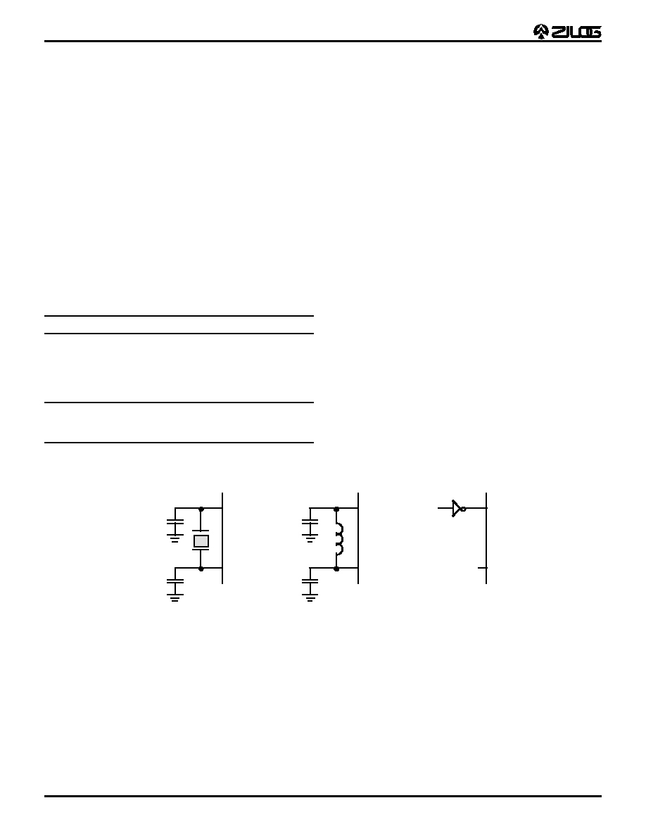
Figure 21. Oscillator Configuration
XTAL1
XTAL2
C1
C2
C1
C2
XTAL1
XTAL2
XTAL1
XTAL2
Ceramic Resonator or
Crystal
C1, C2 = 47 pF TYP *
f = 8 MHz
LC
C1, C2 = 22 pF
L = 130 uH *
f = 3 MHz *
External Clock
L
* Preliminary value including pin parasitics
* * Device ground pin
VSS* *
VSS* *
VSS* *
VSS* *
Z86C83/C84
Z8
Æ
MCU Microcontrollers
28
DS96DZ80203
Analog-to-Digital Converter
The Analog-to-Digital (ADC) is an 8-bit half flash converter
that uses two reference resistor ladders for its upper 4 bits
(MSBs) and lower 4 bits (LSBs) conversion. Two reference
voltage pins, AV
CC
and A
GND
, are provided for external
reference voltage supplies. During the sampling period
from one of the eight channel inputs, the converter is also
being auto-zeroed before starting the conversion. The
conversion time is dependent on the internal clock
frequency. The minimum conversion time is 35 X
SCLK(see Figure 22).
The ADC is controlled by the Z8
Æ
and its three registers
(two Control and one Result) are mapped into the
Extended Register File. A conversion can be initiated by
writing to the ADC Control Register 0 after the ADC
Control Register 1 is configured.
The start command is implemented in such a way as to
begin a conversion at any time, if a conversion is in
progress and a new start command is received, then the
conversion in progress will be aborted and a new
conversion will be initiated. This allows the programmed
values to be changed without affecting a conversion-in-
progress. The new values will take effect only after a new
start command is received.
The ADC can be disabled (for low power) or enabled by a
Control Register bit.
Though the ADC will function for a smaller input voltage
and voltage reference, the noise and offsets remain
constant over the specified electrical range. The errors of
the converter will increase and the conversion time may
also take slightly longer due to smaller input signals.
ADC Calibration Offset
Specially matched resistors are program-enabled to allow
35.0 percent or 50 percent offset from A
GND
. They may
selectively enable these resistors to offset the A
GND
by 35.0
percent (2.5V to 5V) or 50 percent (1.75V to 5V) thereby
allowing the 8-bit ADC across a narrower voltage range.
This will allow significant resolution improvement within
the reduced voltage range.
Note: The AV
CC
must be the same value as V
CC
and A
GND
must be the same value as GND.
Figure 22. ADC Architecture
Start
Converter
A/D
Control
Reg.
8
8
8
A/D
Result
Reg.
A/D
Converter
AV
CC
A
GND
A/D
Control
Reg.
8
Selected
Channel
EXT
Sample
and
Hold
ADC Register
9
D4, D5
4
Calibration Offset
ADC0
ADR1
ADC1
Vref +
Vcc
Vref -
GND
Z86C83/C84
Z8
Æ
MCU Microcontrollers
29
DS96DZ80203
FUNCTIONAL DESCRIPTION (Continued)
Channel Select (bits 2, 1, 0).
ADE (bit 7). A zero disables any A/D conversions or
accessing any ADC registers except writing to ADE bit. A
one Enables all ADC accesses. ADC result register is
shown in Figure 25.
Figure 23. ADC Control Register 0 (Read/Write)
SCAN
0
No action*
1
Convert channel then stop
CSEL2
CSEL1
CSEL0
Channel
0
0
0
0 (P20)*
0
0
1
1 (P21)
0
1
0
2 (P22)
0
1
1
3 (P23)
1
0
0
4 (P24)
1
0
1
5 (P25)
1
1
0
6 (P26)
1
1
1
7 (P27)
Note: *The desired P2 bit must be set equal 1 to allow Port bit
ias ADC input.
Figure 24. ADC Control Register 1 (Read/Write)
D7
D6
D5
D4
D3
D2
D1
D0
CSEL0
CSEL1
CSEL2
ADC0 (A) Bank C, Register 8
SCAN
0 = No action. *
1 = Convert, then stop.
A
IN
/Input/Output Control
0 = No action *
1 = Enable selected channel
(D
2
,D
1
,D
0
) as analog input
on associated Port 20-27
Must be D7 = 0
D6 = 0
D5 = 1
* Default After Reset
D7
D6
D5
D4
D3
D2
D1
D0
ADC1 Bank C, Register 9
ADE
0 Disable*
1 Enable
Must be 0.
D5 D4
0 0 50 % AGND Offset
1 0 35% AGND Offset
0 1 Reserved
1 1 No Offset
Reserved (Must be 1.)
Figure 25. Result Register (Read-Only)
Figure 26. Bank C
Data
D7 D6
D5
D4
D3
D2
D1
D0
ADR Bank C, Register A
Reg F
Reg E
Reg D
Reg C
Reg B
Reg A
Reg 9
Reg 8
AD Control 0
Reg 7
Reg 6
Reg 5
Reg 4
Reg 3
Reg 2
Reg 1
Reg 0
AD Control 1
AD Result 1
These registers
can be accessed.
Z86C83/C84
Z8
Æ
MCU Microcontrollers
30
DS96DZ80203
Figure 27 shows the input circuit of the ADC. When
conversion starts the analog input voltage is connected to
the MSB and LSB flash converter inputs as shown in the
Input Impedance CKT diagram. Effectively, shunting 31
parallel internal resistance of the analog switches and
simultaneously charging 31 parallel 0.5 pF capacitors,
which is equivalent to seeing a 400 Ohms input impedance
in parallel with a 16 pF capacitor. Other input stray
capacitance adds about 10 pF to the input load. For input
source resistances up to 2 kOhms can be used under
normal operating condition without any degradation of the
input settling time. For larger input source resistance,
longer conversion cycle time may be required to
compensate the input settling time problem.
Typical Z8 A/D Conversion Sequence
1.
Set the register pointer to Extended Bank (C),that is,
SRP #%0C instruction.
2.
Next, set ADE flag by loading ADC1 Control Register
Bank (C) Register 9, bit 7. Also, load bits 0-4 of this
same register to select a AV
CC
or A
GND
offset value. A
precision voltage divider connected to the A/D
resistive ladder can offset conversion dynamic range
to specified limits within the AV
CC
and A
GND
limits. By
loading Bank (C) Register 9, bits 0-4, with the
appropriate value it is possible to select from these
groups:
a.
No Offset. The Converter Dynamic range is from
0V to 5.0V for AV
CC
= 5.0V.
b.
35 Percent A
GND
Offset. The Converter Dynamic
range is 1.75V - 5.0V for AV
CC
= 5.0V.
c.
50 Percent A
GND
Offset. The Converter Dynamic
range is 2.5V - 5.0V for AV
CC
= 5.0V.
3.
Select one of the eight A/D inputs for conversion by
loading Bank (C) Register 8 with the desired attributes:
Bits 0 - 2 select an A/D input, bits 3 and 4 select A/D
conversion (or digital port I/O).
4.
Set Bank (C) Register 8, bit 3 to enable A/D
conversion. (This flag can be set concurrently with
step 3.) This flag is automatically reset when the A/D
conversion is completed, so a bit test can be
performed to determine A/D readiness if necessary.
5.
Read the A/D result in Bank (C) Register A. Please
note that the A/D result is not valid (indeterminate)
unless ADE flag (Register 9, bit 7) was previously set,
otherwise A/D converter output is tri-stated.
Figure 27. Input Impedance of ADC
CMOS Switch
on Resistance
2 - 5 k
C Parasitic
R Source
C .5 pF
V Ref
C .5 pF
C .5 pF
31 CMOS Digital
Comparators
V Ref
V Ref
Z86C83/C84
Z8
Æ
MCU Microcontrollers
31
DS96DZ80203
FUNCTIONAL DESCRIPTION (Continued)
Digital-to-Analog Converters
The Z86C84 has two Digital-to-Analog Converters
(DACs). Each DAC is an 8-bit resistor string, with a
programmable 0.25X, 0.5X, or 1X gain output buffer. The
DAC output voltage settles after the internal data is latched
into the DAC Data register. The top and bottom ends of the
resistor ladder are register-selected to be connected to
either the analog supply rails, AV
CC
and A
GND
, or two
externally-provided reference voltages, VDHI and VDLO.
External references are recommended to explicitly set the
DAC output limits. Since the gain stage cannot drive to the
supply rails, VDHI and VDLO must be within ranges shown
in the specifications. If either reference approaches the
analog supply rails, the output will be unable to span the
reference voltage range. The externally provided
reference voltages should not exceed the supply voltages.
The DAC outputs are latch-up protected and can drive
output loads (Figure 28).
Note: The AV
CC
must be the same value as V
CC
and A
GND
must be the same value as GND
Figure 28. DAC Block Diagram
Programmable
Gain
Data
Bus
8-Bit
Resistor
Ladder
8
8
DACn
Data
Register
DACRn
Control
Register
8
Analog
+
-
AVCC
DAC1
or
DAC2
* Bits 0, 1
AGND
PAD
PAD
VDLO
High
PAD
VDHI
Note:
* DACRn Control Register Bits
Low
(n = 1 or 2)
Z86C83/C84
Z8
Æ
MCU Microcontrollers
32
DS96DZ80203
The D/A conversion for DAC1 is driven by writing 8-bit data
to the DAC1 data register (Bank C, Register 06H). The
D/A conversion for DAC 2 is controlled by the DAC2 data
register (Bank C, Register 07H). Each DAC data register
is initialized to midrange 80H on power-up.
There are two DAC control registers: DACR1 (Bank C,
Register 04H) for DAC1, and DACR2 (Bank C, Register
05H) for DAC2. Control register bits 0 and 1 set the DAC
gain. When DAC data is 80H, the DAC output is constant
for any gain setting (Figure 29 and Figure 31).
Figure 29. D/A 1 Control Register
Figure 30. D/A 1 Data Register
D7
D6
D5
D4
D3
D2
D1
D0
DAC1 Gain
0 0 1 X
0 1 1/2 X
1 0 1 Not Used
1 1 1/4 X
DACR1 Bank C, Register 4
DAC1 Enable
0 Disable
1 Enable
Reserved (Must be 0)
D7
D6
D5
D4
D3
D2
D1
D0
DAC1 Bank C, Register 6
0 = Low Level
1 = High Level
Figure 31. D/A 2 Control Register
Figure 32. D/A 2 Data Register
D7
D6
D5
D4
D3
D2
D1
D0
DAC2 Gain
0 0 1 X
0 1 1/2 X
1 0 1 Not Used
1 1 1/4 X
DACR2 Bank C, Register 5
DAC2 Enable
0 Disable
1 Enable
Reserved (Must be 0)
D7
D6
D5
D4
D3
D2
D1
D0
DAC2 Bank C, Register 7
= Low Level
= High Level
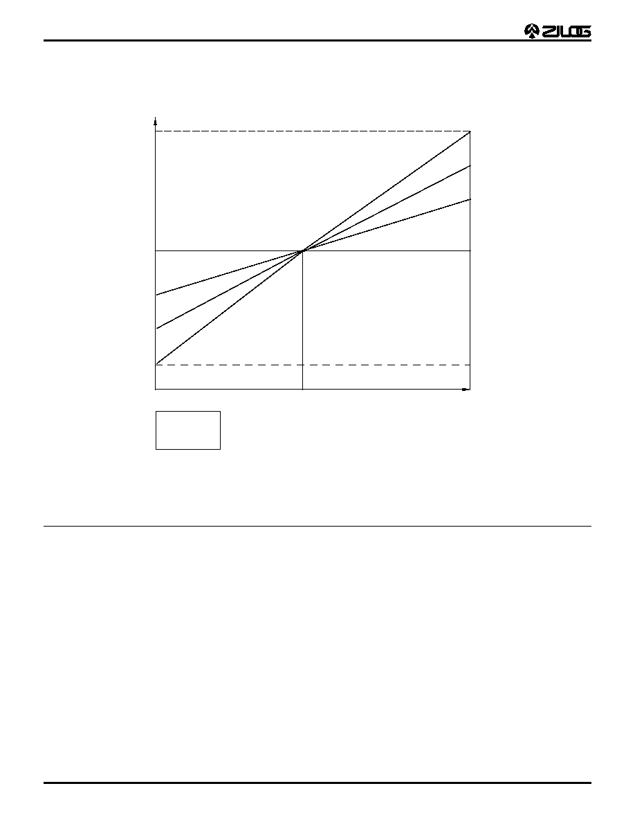
Z86C83/C84
Z8
Æ
MCU Microcontrollers
33
DS96DZ80203
FUNCTIONAL DESCRIPTION (Continued)
Power-On Reset (POR). A timer circuit clocked by a
dedicated on-board RC oscillator or by the XTAL oscillator
is used for the POR timer function. The POR time allows
V
CC
and the oscillator circuit to stabilize before instruction
execution begins. The POR timer circuit is a one-shot timer
triggered by one of three conditions:
s
Power Fail to Power OK Status
s
Stop-Mode Recovery (If D5 of SMR Register = 1)
s
WDT Time-Out (Including from Stop Mode)
The POR time is T
POR
minimum. Bit 5 of the STOP Mode
Register determines whether the POR timer is bypassed
after Stop-Mode Recovery (typical for external clock, and
RC/LC oscillators with fast start up time).
HALT. Turns off the internal CPU clock but not the XTAL
oscillation. The counter/timers and external interrupts
IRQ0, IRQ1, and IRQ2 remain active. The device is
recovered by interrupts, either externally or internally
generated (a POR or a WDT time-out). An interrupt
request must be executed (enabled) to exit HALT mode.
After the interrupt service routine, the program continues
from the instruction after the HALT. In case of a POR or a
WDT time-out, program execution will restart at address
000CH.
STOP. This instruction turns off the internal clock and
external crystal oscillation and reduces the standby
current to 10
µ
A (typical) or less. The STOP mode is
terminated by a reset of either WDT time-out, POR, or
Stop-Mode Recovery. This causes the processor to restart
the application program at address 000CH.
Figure 33. Gain Control on DAC
3.5
3.05
2.6
2.15
2% accuracy
1.7
1.26
.8
VDLO
0
80H
FFH
3.5V
VDHI
1/4X
1/2X
1X
DAC Output in Volts
2.15
DAC Data Register Value
Notes:
Vcc = 5.0V
±
10%
VDHI = 3.5V
VDLO = 0.8V
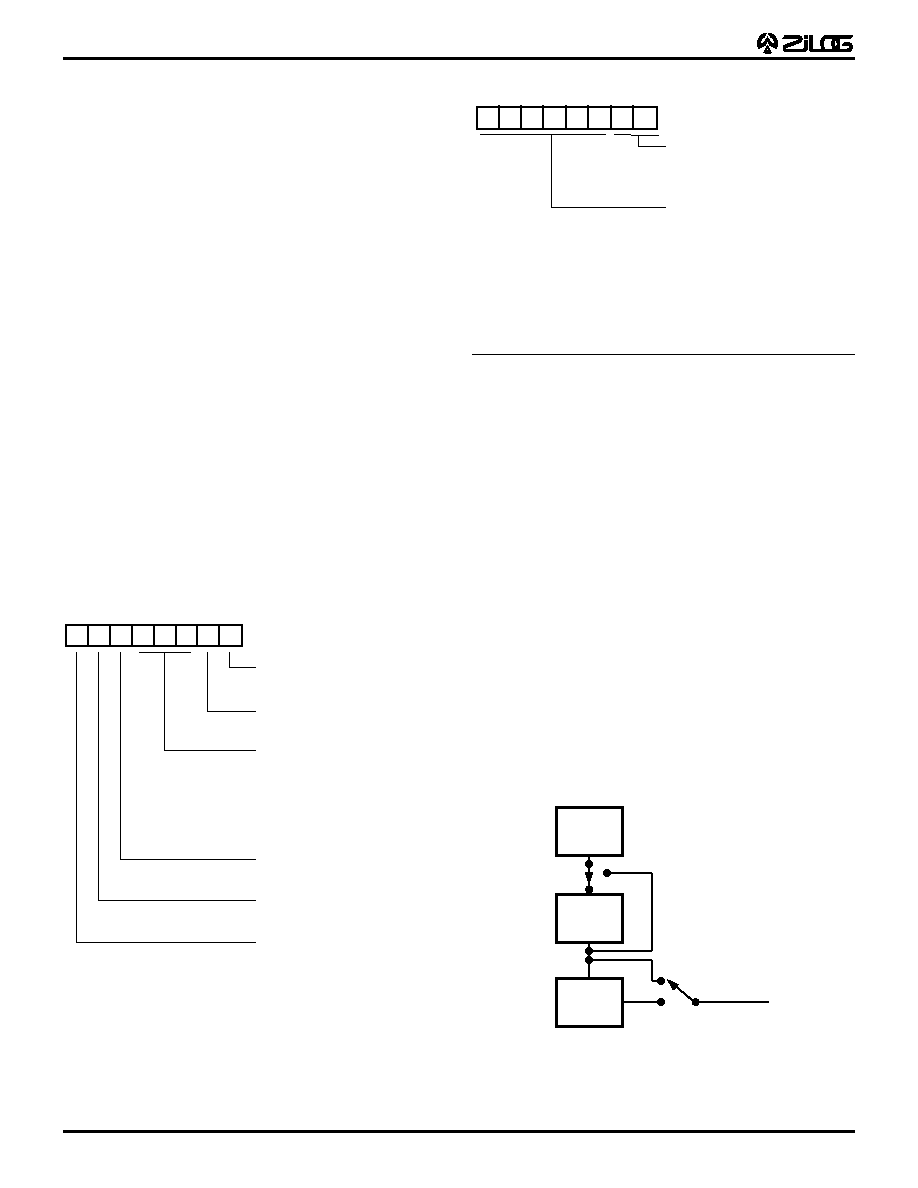
Z86C83/C84
Z8
Æ
MCU Microcontrollers
34
DS96DZ80203
In order to enter STOP (or HALT) mode, it is necessary to
first flush the instruction pipeline to avoid suspending
execution in mid-instruction. To do this, the user must
execute a NOP (opcode = FFH) immediately before the
appropriate sleep instruction, that is,
STOP-Mode Recovery (SMR) Register. This register se-
lects the clock divide value and determines the mode of
STOP-Mode Recovery (Figure 34 and Figure 35). All bits
are Write-Only, except bit 7, which is Read-Only. Bit 7 is a
flag bit that is hardware set on the condition of STOP re-
covery and reset by a power-on cycle. Bit 6 controls wheth-
er a low level or a high level is required from the recovery
source. Bit 5 controls the reset delay after recovery. Bits 2,
3, and 4, or the SMR Register, specify the source of the
STOP-Mode Recovery signal. Bits 0 and 1 determine the
timeout period of the WDT. The SMR Register is located in
Bank F of the Expanded Register Group at address 0BH.
When the Stop-Mode Recovery sources are selected in
this register, then SMR2 Register bits D0,D1 must be set
to 0.
SCLK/TCLK Divide-by-16 Select (D0). D0 of the SMR
controls a divide-by-16 prescaler of SCLK/TCLK. The
control selectively reduces device power consumption
during normal processor execution (SCLK control) and/or
HALT mode (where TCLK sources counter/timers and
interrupt logic). This bit is reset to D0 = 0 after a Stop-Mode
Recovery, WDT Timeout, and POR.
External Clock Divide-by-Two (D1). This bit can elimi-
nate the oscillator divide-by-two circuitry. When this bit is
0, the System Clock (SCLK) and Timer Clock (TCLK) are
equal to the external clock frequency divided by two. The
SCLK/TCLK is equal to the external clock frequency when
this bit is set (D1=1). Using this bit together with D7 of
PCON further helps lower EMI (that is, D7 (PCON) = 0, D1
(SMR) = 1). The default setting is zero. Maximum external
clock frequency is 4 MHz when SMR Bit D1 = 1 where
SCLK/TCLK = XTAL.
FF
NOP
; clear the pipeline
6F
STOP
; enter STOP mode
or
FF
NOP
; clear the pipeline
7F
HALT
; enter HALT mode
Figure 34. STOP-Mode Recovery Register (Write-
Only Except Bit D7, Which Is Read-Only)
D7
D6 D5
D4
D3
D2
D1
D0
SMR (FH) 0B
SCLK/TCLK Divide-by-16
0 OFF* *
1 ON
Stop-Mode Recovery Source
000 POR Only and/or External Reset*
001 Reserved
010 P31
011 P32
100 P33
101 P27
110 P2 NOR 0-3
111 P2 NOR 0-7
Stop Delay
0 OFF
1 ON
Stop Recovery Level
0 Low *
1 High
Stop Flag (Read-Only)
0 POR
1 Stop Recovery
Note: Not used in conjunction with SMR2
Source
* Default Setting After RESET
** Default setting after RESET and
Stop-Mode Recovery
*
*
External Clock Divide-by-2
0 SCLK/TCLK = XTAL/2*
1 SCLK/TCLK = XTAL
Figure 35. Stop-Mode Recovery Register 2
([0F] DH: Write-Only)
Figure 36. SCLK Circuit
D7
D6
D5
D4
D3
D2
D1
D0
SMR2 (0F) DH
Note: Not used in conjunction with SMR Source
Stop-Mode Recovery Source 2
00 POR only*
01 AND P20,P21,P22,P23
10 AND P20,P21,P22,P23,
P24,P25,P26,P27
Reserved (Must be 0)
SMR, D0
˜
2
˜
16
OSC
SCLK
TCLK
SMR, D1

Z86C83/C84
Z8
Æ
MCU Microcontrollers
35
DS96DZ80203
FUNCTIONAL DESCRIPTION (Continued)
STOP-Mode Recovery Source (D2, D3, and D4).
These three bits of the SMR register specify the wake-up
source of the STOP recovery (Figure 37 and Table 12).
When the STOP-Mode Recovery Sources are selected in
this register then SMR2 register bits D0,D1 must be set to
zero. P33-P31 cannot wake up from Stop Mode if the input
lines are configured as analog inputs to the Analog
comparator or Analog-to-Digital Converter since the
Analog Comparator's are powered down in Stop Mode.
Note: If the Port 2 pin is configured as an output, this
output level will be read by the SMR circuitry.
STOP-Mode Recovery Delay Select (D5). This bit, if
High, enables the T
POR
/RESET delay after Stop-Mode
Recovery. The default configuration of this bit is "1". A
POR or WDT reset will override the selection and cause
the reset delay to occur.
STOP-Mode Recovery Edge Select (D6). A "1" in this bit
position indicates that a high level on the output to the
exclusive Or-Gate input from the selected recovery source
wakes the Z86C83/C84 from STOP mode. A "0" indicates
low-level recovery. The default is 0 on POR. This bit is
used for either SMR or SMR2.
Cold or Warm Start (D7). This bit is set by the device
upon entering STOP mode. A 0 in this bit (cold) indicates
that the device resets by POR/WDT reset. A "1" in this bit
(warm) indicates that the device awakens by a Stop-Mode
Recovery source.
Note: A WDT reset out of Stop Mode will also set this bit
to a "1."
STOP-Mode Recovery Register 2 (SMR2). This register
contains additional Stop-Mode Recovery sources. When
the Stop-Mode Recovery sources are selected in this
register then SMR Register Bits D2, D3, and D4 must be 0.
Table 12. STOP-Mode Recovery Source
SMR:432
Operation
D4 D3 D2 Description of Action
0
0
0
POR and/or external reset recovery
0
0
1
Reserved
0
1
0
P31 transition (not in Analog Mode)
0
1
1
P32 transition (not in Analog Mode)
1
0
0
P33 transition (not in Analog Mode)
1
0
1
P27 transition
1
1
0
Logical NOR of P20 through P23
1
1
1
Logical NOR of P20 through P27
Table 13. Stop-Mode Recovery Source
SMR:10
Operation
D1
D0
Description of Action
0
0
SMR2 disables source
0
1
Logical AND of P20 through P23
1
0
Logical AND of P20 through P27
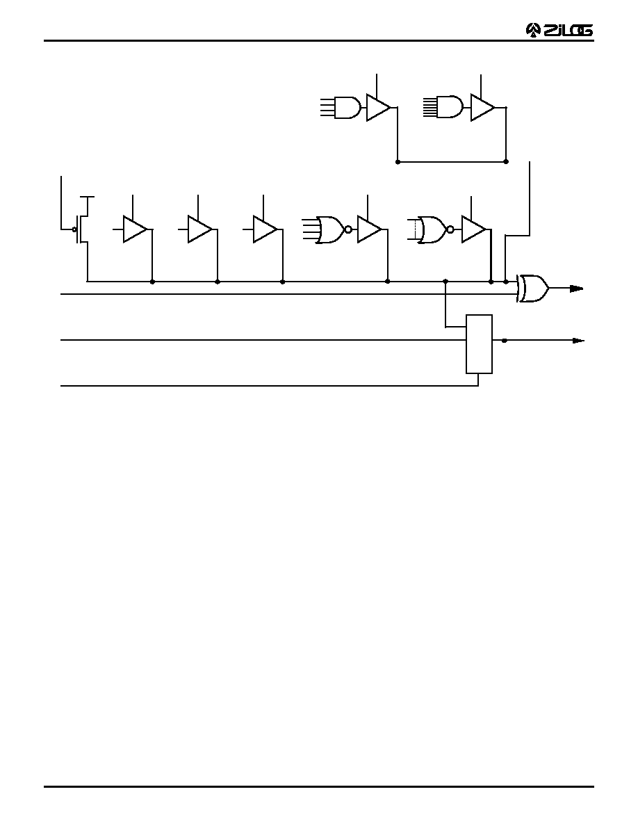
Z86C83/C84
Z8
Æ
MCU Microcontrollers
36
DS96DZ80203
Figure 37. STOP-Mode Recovery Source
P31
P32
P33
P27
Stop-Mode Recovery Edge
Select (SMR)
P33 From Pads
Digital/Analog Mode
Select (P3M)
To P33 Data
Latch and IRQ1
To POR
RESET
SMR
SMR
SMR
D4 D3 D2
0 0 1
0 1 0
0 1 1
D4 D3 D2
1 0 0
D4 D3 D2
1 0 1
MUX
SMR
SMR
D4 D3 D2
1 1 0
D4 D3 D2
1 1 1
P20
P23
P20
P27
SMR2
SMR2
D1 D0
1 1
D1 D0
1 1
P20
P23
P20
P27
SMR
D4 D3 D2
0 0 0
VDD
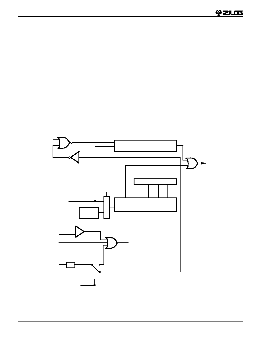
Z86C83/C84
Z8
Æ
MCU Microcontrollers
37
DS96DZ80203
FUNCTIONAL DESCRIPTION (Continued)
Watch-Dog Timer Mode Register (WDTMR). The WDT
is a retriggerable one-shot timer that resets the Z8 if it
reaches its terminal count. The WDT is initially enabled by
executing the WDT instruction and refreshed on
subsequent executions of the WDT instruction. The WDT
circuit is driven by an on-board RC oscillator or external
oscillator from the XTAL1 pin. The POR clock source is
selected with bit 4 of the WDT register (Figure 38).
WDT instruction affects the Z (Zero), S (Sign), and V
(Overflow) flags. The WDTMR must be written to within 64
internal system clocks. After that, the WDTMR is write
protected.
Note: WDT time-out while in Stop-Mode will not reset
SMR, PCON, WDTMR, P2M, P3M, Ports 2 and 3 Data
Registers, but will cause the reset delay to occur.
The Power-On Reset (POR) clock source is selected with
bit 4 of the WDTMR. Bits 0 and 1 control a tap circuit that
determines the time-out period. Bit 2 determines whether
the WDT is active during HALT and bit 3 determines WDT
activity during STOP. If bits 3 and 4 of this register are both
set to "1," the WDT is only driven by the external clock
during STOP mode. This feature makes it possible to wake
up from STOP mode from an internal source. Bits 5
through 7 of the WDTMR are reserved (Figure 39). This
register is accessible only during the first 64 processor
cycles (64 SCLKs) from the execution of the first
instruction after Power-On-Reset, Watch-Dog Reset or a
Stop-Mode Recovery. After this point, the register cannot
be modified by any means, intentional or otherwise. The
WDTMR cannot be read and is located in Bank F of the
Expanded Register group at address location 0FH.
Figure 38. Resets and WDT
CLK
18 Clock RESET
Generator
RESET
Clear
WDT TAP SELECT
RC
OSC.
CK
CLR
128 SCLK
POR
128
SCLK
256
SCLK
512
SCLK
2048
SCLK
3.0V Operating
Voltage Det.
Internal
RESET
WDT Select
(WDTMR)
CK Source
Select
(WDTMR)
XTAL
VCC
3.0V REF.
From Stop
Mode
Recovery
Source
WDT
Stop Delay
Select (SMR D5)
12 ns Glitch Filter
+
-
WDT/POR Counter Chain
M
U
X
/RESET
Z86C83/C84
Z8
Æ
MCU Microcontrollers
38
DS96DZ80203
WDT Time Select (D1, D0). Selects the WDT time-out
period. It is configured as shown in Table 14.
WDT During HALT (D2). This bit determines whether or
not the WDT is active during HALT mode. A "1" indicates
active during HALT. The default is "1."
Note: If WDT is permanently selected (always ON mode),
the WDT will continue to run even if set not to run in STOP
or HALT Mode.
WDT During STOP (D3). This bit determines whether or
not the WDT is active during STOP mode. Since XTAL
clock is stopped during STOP mode, unless as specified
below, the on-board RC has to be selected as the clock
source to the POR counter. A "1" indicates active during
STOP. The default is "1". If bits D3 and D4 are both set to
"1," the WDT only, is driven by the external clock during
STOP mode.
Notes:
1.
If WDT is permanently selected (always ON mode),
the WDT will continue to run even if set not to run in
STOP or HALT Mode.
2.
WDT instructions affect the Z (Zero), S (Sign), and V
(Overflow) flags.
On-Board, Power-On-Reset RC or External XTAL1
Oscillator Select (D4). This bit determines which
oscillator source is used to clock the internal POR and
WDT counter chain. If the bit is a "1," the internal RC
oscillator is bypassed and the POR and WDT clock source
is driven from the external pin, XTAL1. The default
configuration of this bit is 0, which selects the RC
oscillator. If the XTAL1 pin is selected as the oscillator
source for the WDT, during Stop Mode, the oscillator will
be stopped and the WDT will not run. This is true even if
the WDT is selected to run during Stop Mode.
V
CC
Voltage Comparator. An on-board Voltage Compara-
tor checks that V
CC
is at the required level to ensure correct
operation of the device. RESET is globally driven if V
CC
is
below the specified voltage (typically 2.6V).
ROM Protect. ROM Protect is mask-programmable. It is
selected by the customer at the time the ROM code is
submitted.
ROM Mask Selectable Options
There are six ROM mask options that must be selected at
the time the ROM mask is ordered (ROM code submitted).
Figure 39. Watch-Dog Timer Mode Register
(Write Only)
Table 14. WDT Time Select (Min. @ 5.0V)
D1
D0
Time-Out of
Internal RC OSC
Time-Out of
SCLK Clock
0
0
6.25 ms min
256 SCLK
0
1
12.5 ms min
512 SCLK*
1
0
25 ms min
1024 SCLK
1
1
100 ms min
4096 SCLK
Notes:
The default on a WDT initiated reset is 512 SCLK.
The minimum time shown is for V
CC
@ 5.0V.
D7
D6
D5
D4
D3
D2
D1
D0
WDTMR (F) 0F
WDT TAP
00 256 SCLK
01 512 SCLK *
10 1024 SCLK
11 4096 SCLK
WDT During HALT
0 OFF
1 ON
WDT During STOP
0 OFF
1 ON
XTAL1/INT RC Select for WDT
0 On-Board RC
1 XTAL
Reserved (Must be 0)
*
Default setting after RESET
XTAL=SCLK/TCLK shown
*
*
*
Table 15. ROM Mask Selectable Options
Option
Selection
Permanent WDT
Yes/No
Port0 Pull-Ups
Yes/No
Port0 Auto Latches
Yes/No
ROM Protect
Yes/No
RAM Protect
Yes/No
Z86C83/C84
Z8
Æ
MCU Microcontrollers
DS96DZ80203
39
1
EXPANDED REGISTER FILE CONTROL REGISTERS (0C)
Figure 40. ADC Control Register 0 (Read/Write)
Figure 41. ADC Control Register 1 (Read/Write)
Figure 42. AD Result Register (Read Only)
D7 D6
D5
D4
D3
D2
D1
D0
ADC0 (OC) 8H
Scan 0 = No action.*
1 = Convert channel then stop.
A
IN
/Input/Output Control
0 = No Action (Digital Function)*
1 = Enable Selected Channel
(M
2
, M
1
, M
0
) as analog input on
associated Port P27-P20
Channel Select (bits 2,1,0)
CSEL2
0
0
0
0
1
1
1
1
CSEL1
0
0
1
1
0
0
1
1
CSEL0
0
1
0
1
0
1
0
1
Channel
0*
1
2
3
4
5
6
7
* Default setting after reset.
Must be 0 0 1
D7
D6
D5
D4
D3
D2
D1
D0
ADC1 Bank C, Register 9
ADE
0 Disable*
1 Enable
Must be 0.
D5 D4
0 0 50 % AGND Offset
1 0 35% AGND Offset
0 1 Reserved
1 1 No Offset
Reserved (Must be 1.)
D7 D6
D5
D4
D3
D2
D1
D0
ADR1 (OC) AH
Data
Figure 43. D/A 1 Control Register
Figure 44. D/A 2 Control Register
Figure 45. D/A 1 Data Register
Figure 46. D/A 2 Data Register
D7
D6
D5
D4
D3
D2
D1
D0
DAC1 Gain
0 0 1 X
0 1 1/2 X
1 0 1 Not Used
1 1 1/4 X
DACR1 Bank C, Register 4
DAC1 Enable
0 Disable
1 Enable
Reserved (Must be 0)
D7
D6
D5
D4
D3
D2
D1
D0
DAC2 Gain
0 0 1 X
0 1 1/2 X
1 0 1 Not Used
1 1 1/4 X
DACR2 Bank C, Register 5
DAC2 Enable
0 Disable
1 Enable
Reserved (Must be 0)
D7
D6
D5
D4
D3
D2
D1
D0
DAC1 Bank C, Register 6
0 = Low Level
1 = High Level
D7
D6
D5
D4
D3
D2
D1
D0
DAC2 Bank C, Register 7
0 = Low Level
1 = High Level
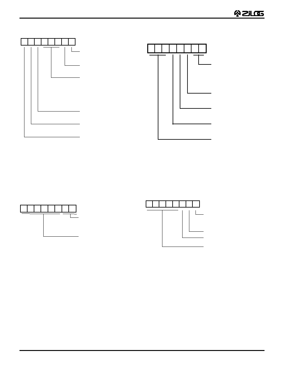
Z86C83/C84
Z8
Æ
MCU Microcontrollers
40
DS96DZ80203
EXPANDED REGISTER FILE CONTROL REGISTERS
Figure 47. Stop-Mode Recovery Register
(Write-Only, except Bit 7 which is Read-Only)
Figure 48. Watch-Dog Timer Mode Register 2
D7
D6 D5
D4
D3
D2
D1
D0
(
)
SCLK/TCLK Divide-by-16
0 OFF* *
1 ON
Stop-Mode Recovery Source
000 POR Only and/or External Reset*
001 Reserved
010 P31
011 P32
100 P33
101 P27
110 P2 NOR 0-3
111 P2 NOR 0-7
Stop Delay
0 OFF
1 ON
Stop Recovery Level
0 Low *
1 High
Stop Flag (Read-Only)
0 POR
1 Stop Recovery
Note: Not used in conjunction with SMR2
Source
* Default Setting After RESET
** Default setting after RESET and
Stop-Mode Recovery
*
*
External Clock Divide-by-2
0 SCLK/TCLK = XTAL/2*
1 SCLK/TCLK = XTAL
D7
D6
D5
D4
D3
D2
D1
D0
SMR2 (0F) DH
Note: Not used in conjunction with SMR Source
Stop-Mode Recovery Source 2
00 POR only*
01 AND P20,P21,P22,P23
10 AND P20,P21,P22,P23,
P24,P25,P26,P27
Reserved (Must be 0)
Figure 49. Watch-Dog Timer Mode Register
(Write-Only)
Figure 50. Port Configuration Register (PCON)
(Write-Only)
D7 D6 D5 D4 D3 D2 D1 D0
WDTMR (F) 0F
WDT TAP
00 256 SCLK
01 512 SCLK *
10 1024 SCLK
11 4096 SCLK
WDT During HALT
0 OFF
1 ON
WDT During STOP
0 OFF
1 ON
XTAL1/INT RC Select for WDT
0 On-Board RC
1 XTAL
Reserved (Must be 0)
*
Default setting after RESET
XTAL=SCLK/TCLK shown
*
*
*
D7
D6
D5
D4
D3
D2
D1
D0
Comparator
Output Port 3
0 P34 Standard Output
*
1 P34 Comparator Output
Reserved (Must be 1.)
PCON (F) 00
* Default setting from Stop-Mode Recovery,
Power-On Reset, and any WDT Reset.
0 Port 0 Open-Drain
1 Port 0 Push-Pull*
Reserved (Must be 1.)
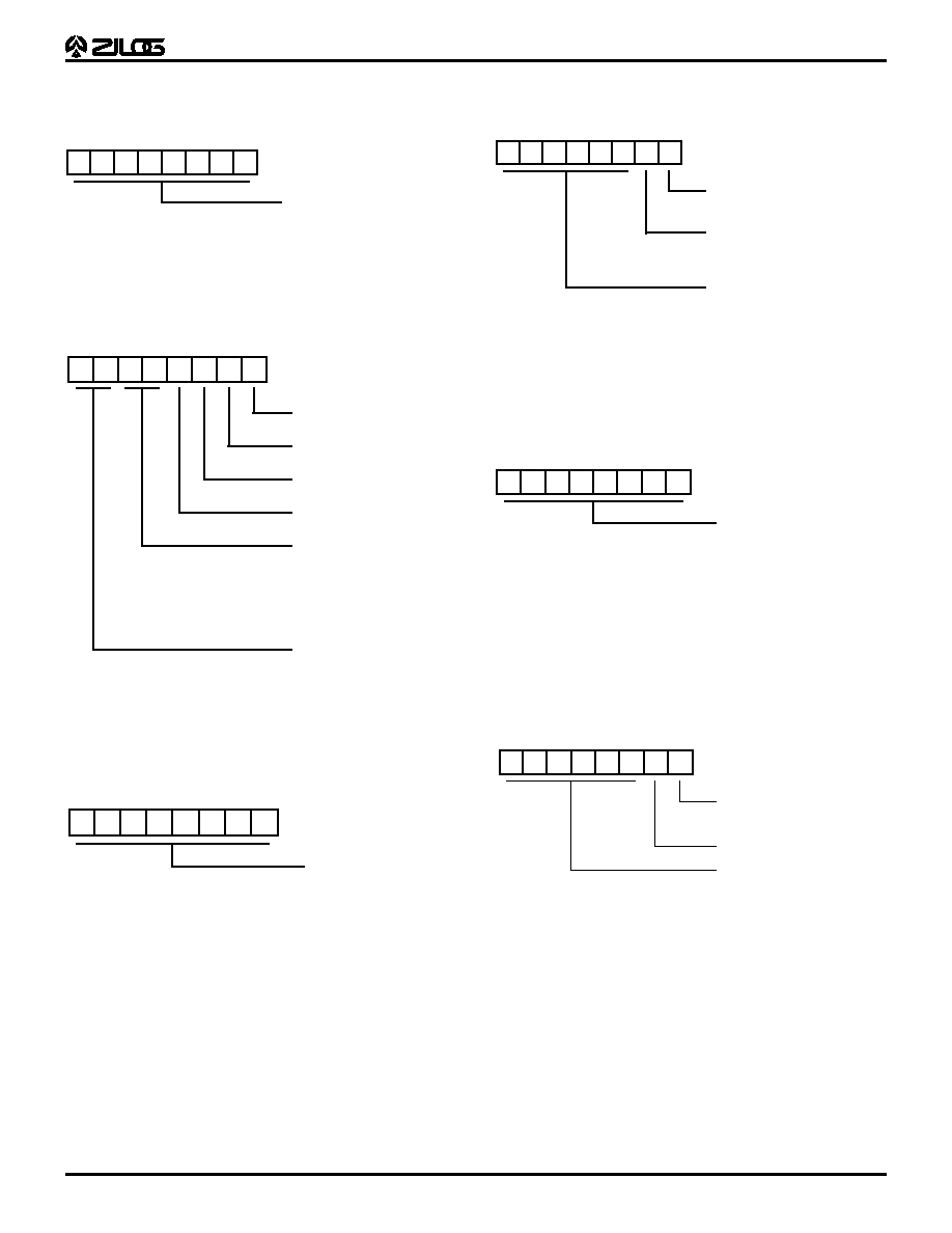
Z86C83/C84
Z8
Æ
MCU Microcontrollers
DS96DZ80203
41
1
Z8
CONTROL REGISTERS
Figure 51. Reserved
Figure 52. Timer Mode Register (F1
H
: Read/Write)
Figure 53. Counter/Timer 1 Register (F2
H
: Read/Write)
D7
D6
D5
D4
D3
D2
D1
D0
Reserved (Must be 0)
R240
D7 D6
D5
D4
D3 D2
D1
D0
0 Disable T0 Count
1 Enable T0 Count
0 No Function
1 Load T0
0 No Function
1 Load T1
0 Disable T1 Count
1 Enable T1 Count
TIN Modes
00 External Clock Input
01 Gate Input
10 Trigger Input
(Non-retriggerable)
11 Trigger Input
(Retriggerable)
Reserved (Must be 0)
R241 TMR
D7
D6
D5
D4
D3
D2
D1
D0
T1 Initial Value
(When Written)
(Range 1-256 Decimal
01-00 HEX)
T1 Current Value
(When READ)
R242 T1
Figure 54. Prescaler 1 Register (F3
H
: Write-Only)
Figure 55. Counter/Timer 0 Register (F4
H
: Read/Write)
Figure 56. Prescaler 0 Register (F5
H
: Write-Only)
D7
D6
D5
D4
D3
D2
D1
D0
Count Mode
0 T1 Single Pass
1 T1 Modulo
Clock Source
1 T1 Internal
0 T1 External Timing Input
(TIN) Mode
Prescaler Modulo
(Range: 1-64 Decimal
01-00 HEX)
R243 PRE1
D7
D6
D5
D4
D3
D2
D1
D0
T0 Initial Value
(When Written)
(Range: 1-256 Decimal
01-00 HEX)
T0 Current Value
(When READ)
R244 T0
D7
D6
D5
D4
D3
D2
D1
D0
Count Mode
0 T0 Single Pass
1 T0 Modulo N
Reserved (Must be 0.)
R245 PRE0
Prescaler Modulo
(Range: 1-64 Decimal
01-00 Hex)
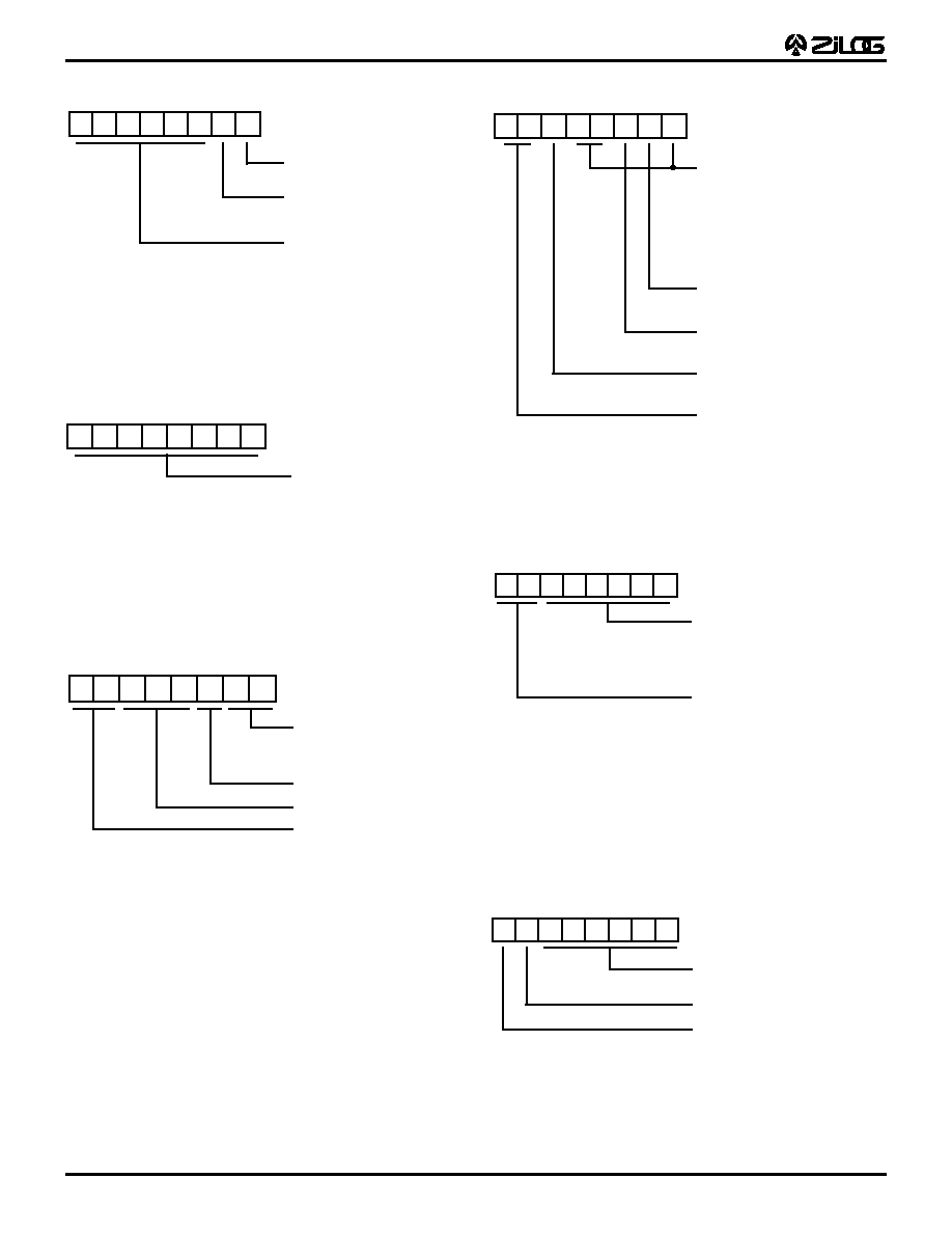
Z86C83/C84
Z8
Æ
MCU Microcontrollers
42
DS96DZ80203
Figure 57. Port 3 Mode Register (F7
H
: Write-Only)
Figure 58. Port 2 Mode Register (F6
H
: Write-Only)
Figure 59. Port 0 and 1 Mode Register
(F8
H
: Write-Only)
D7 D6
D5 D4
D3 D2
D1
D0
0 Port 2 Open-Drain*
1 Port 2 Push-Pull
Port 3 Inputs
0 Digital*
1 Analog
Reserved (Must be 0)
R247 P3M
*Default Setting After Reset
D7
D6
D5
D4
D3
D2
D1
D0
P27- P20 I/O Definition
0 Defines Bit as OUTPUT
1 Defines Bit as INPUT*
R246 P2M
*Default Setting After Reset
D7
D6
D5
D4
D3
D2
D1
D0
P00-P03 Mode
00 Output
01 Input *
1X A11-A8
R248 P01M
Reserved (Must be 1)
Reserved (Must be 0)
P04-P06 Mode
00 Output
01 Input *
1X A15-A12
Not available for
Z86C82, but must be set to 00.
Figure 60. Interrupt Priority Register (F9
H
: Write-Only)
Figure 61. Interrupt Request Register
(F
AH
: Read/Write)
Figure 62. Interrupt Mask Register (F
BH
: Read/Write)
D7
D6
D5
D4
D3
D2
D1
D0
Interrupt Group Priority
000 Reserved
001 C > A > B
010 A > B > C
011 A > C > B
100 B > C > A
101 C > B > A
110 B > A > C
111 Reserved
IRQ3, IRQ5 Priority (Group A)
0 IRQ5 > IRQ3
1 IRQ3 > IRQ5
IRQ0, IRQ2 Priority (Group B)
0 IRQ2 > IRQ0
1 IRQ0 > IRQ2
IRQ1, IRQ4 Priority (Group C)
0 IRQ1 > IRQ4
1 IRQ4 > IRQ1
Reserved (Must be 0)
R249 IPR
D7
D6
D5
D4
D3
D2
D1
D0
IRQ0 = P32 Input
IRQ1 = P33 Input
IRQ2 = P31 Input
IRQ3 = Software Controlled
IRQ4 = T0
IRQ5 = T1
Inter Edge
00 P31
01 P31
10 P31
11 P31
R250 IRQ
Default Setting After Reset = 00H
P32
P32
P32
P32
D7 D6
D5
D4
D3
D2
D1
D0
1 RAM Protect Enabled
0 RAM Protect Disabled *
1 Enables IRQ5-IRQ0
(D0 = IRQ0)
1 Enables Interrupts
0 Disable interrupts *
* (Default setting after RESET.)
R251 IMR
This option must be selected when
ROM code is submitted for Rom Masking;
otherwise, this control bit is disabled
permanently.
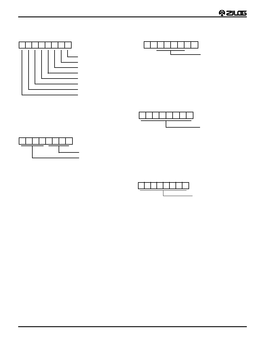
Z86C83/C84
Z8
Æ
MCU Microcontrollers
43
DS96DZ80203
Z8 CONTROL REGISTERS (Continued)
Figure 63. Flag Register (F
CH
: Read/Write)
Figure 64. Register Pointer (F
DH
: Read/Write)
D7
D6
D5
D4
D3
D2
D1
D0
User Flag F1
User Flag F2
Half Carry Flag
Decimal Adjust Flag
Overflow Flag
Sign Flag
Zero Flag
Carry Flag
R252 Flags
D7
D6
D5
D4
D3
D2
D1
D0
Expanded Register Group
Working Register Group
R253 RP
Note: Default Setting After Reset = 00000000
Figure 65. General-Purpose Register
(F
EH
: Read/Write)
Figure 66. Stack Pointer (F
FH
: Read/Write)
Figure 67. Port 2 Pull-up Register
D7
D6
D5
D4
D3
D2
D1
D0
R254 GPR
0 = Low Level
1 = High Level
Default Setting After Reset = 00H
D7
D6
D5
D4
D3
D2
D1
D0
Stack Pointer Lower
Byte (SP7-SP0)
R255 SPL
0 = Low Level
1 = High Level
Default Setting After Reset = 00H
D7
D6
D5
D4
D3
D2
D1
D0
Port 2 (P27-P20) 10K Pull-up
0 = Disabled
1 = Enabled
P2RES Bank C, Register 3
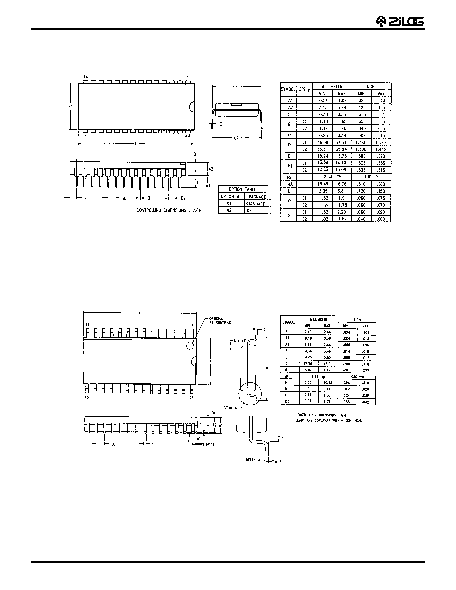
Z86C83/C84
Z8
Æ
MCU Microcontrollers
44
DS96DZ80203
PACKAGE INFORMATION
Figure 68. 28-Pin DIP Package Diagram
Figure 69. 28-Pin SOIC Package Diagram
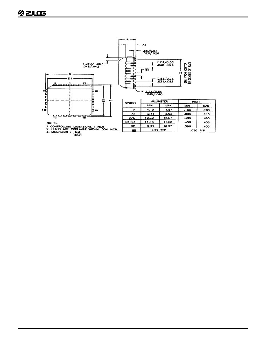
Z86C83/C84
Z8
Æ
MCU Microcontrollers
DS96DZ80203
45
1
Figure 70. 28--Pin PLCC Package Diagram

Z86C83/C84
Z8
Æ
MCU Microcontrollers
46
DS96DZ80203
ORDERING INFORMATION
For fast results, contact your local Zilog sales office for assistance in ordering the part desired.
CODES
Package
P = Plastic DIP
S = Plastic SOIC
Temperature
S = 0
∞
C to + 70
∞
C
E = -40
∞
C to +105
∞
C
Speed
16 = 16 MHz
Environmental
C = Plastic Standard
Z86C83
16 MHz
28-Pin DIP
28-Pin SOIC
28-Pin PLCC
Z86C8316PSC
Z86C8316SSC
Z86C8316VSC
Z86C8316PEC
Z86C8316SEC
Z86C8316VEC
Z86C84
16 MHz
28-Pin DIP
28-Pin SOIC
28-Pin PLCC
Z86C8416PSC
Z86C8416SSC
Z86C8416VSC
Z86C8416PEC
Z86C8416SEC
Z86C8416VEC
Example:
Z 86C83 16 P S C is a Z86C83, 16 MHz, DIP, 0
∞
to +70
∞
C, Plastic Standard Flow
Environmental Flow
Temperature
Package
Speed
Product Number
Zilog Prefix