 | –≠–ª–µ–∫—Ç—Ä–æ–Ω–Ω—ã–π –∫–æ–º–ø–æ–Ω–µ–Ω—Ç: Z86C95 | –°–∫–∞—á–∞—Ç—å:  PDF PDF  ZIP ZIP |
1
Z86C95 DSP
CPS DC-4067-13
GENERAL DESCRIPTION
The Z86C95 MCU (Microcontroller Unit ) introduces a new
level of sophistication to SuperintegrationTM ICs. The
Z86C95 is a member of the Z8
Æ
single-chip microcontroller
family incorporating a CMOS ROMless Z8 microcontroller
with an embedded DSP processor for digital servo control.
The DSP slave processor can perform 16-bit x 16-bit
multiplicates and accumulates in one clock cycle. Addi-
tionally, the Z86C95 is further enhanced with a hardwired
16-bitx16-bit multiplier and a 32-bit/16-bit divider, three
16-bit counter timers with capture and compare registers,
a half flash 8-channel 8-bit A/D converter with a 2
µ
sec
conversion time, an 8-bit DAC with 1/4 programmable gain
stage, UART, serial peripheral interface, and a PWM
output channel (Functional Block Diagram). It is fabricated
using CMOS technology and offered in an 80-pin QFP, 84-
pin PLCC, or 100-pin VQFP package.
The Z86C95 provides up to 16 output address lines thus
permitting an address space of up to 64 Kbytes of data and
program memory each. Eight address outputs (AD7-AD0)
are provided by a multiplexed, 8-bit, Address/Data bus.
The remaining 8 bits are provided via output address bits
A15-A8.
DC-4067-13
(5-17-94)
There are 256 registers located on chip and organized as
236 general-purpose registers, 16 control and status reg-
isters, and four I/O port registers. The register file can be
divided into sixteen groups of 16 working registers each.
Configuration of the registers in this manner allows the use
of short format instructions; in addition, any of the indi-
vidual registers can be accessed directly. Also, the Z86C95
contains 512 bytes of DSP Program RAM and 128 words
of DSP data RAM.
Notes:
All Signals with a preceding front slash, "/", are active Low, e.g.:
B//W (WORD is active Low); /B/W (BYTE is active Low, only).
Power connections follow conventional descriptions below:
Connection
Circuit
Device
Power
V
CC
V
DD
Ground
GND
V
SS
OPERATING ERRATA
Z86C95
CMOS Z8
Æ
D
IGITAL
S
IGNAL
P
ROCESSOR
(DSP)
C
USTOMER
P
ROCUREMENT
S
PECIFICATION
This notice only applies to devices top marked "Z86C9524
ASC/FSC/VSC" with a date code of 9237 or later.
1.
A DSP load to the DAC Register fails below approxi-
mately V
CC
= 4.7V.
2.
Clipping occurs in the linearity of the DAC with a 100K
load at about 3.3V output (VDHI = 3.5V).
3.
I
CC
1 at HALT Mode will show a current of 17-18 mA,
then will jump to 40-70 mA, and will settle between 17-
24 mA. Settling time is about 10-15 seconds.
4.
I
CC
2 at STOP Mode and DSP Pause will show a current
of 1-2 mA, then will jump to 5-7 mA, and will settle at 3-
4 mA. Settling time is about 10-15 seconds.
The following operating errata only applies to devices
topmarked with "Z86C95 ASC/FSC/VSC."
1.
ICC1 at HALT Mode will show a current of 17-18 mA,
then will jump to 40-70 mA, and will settle between 17-
24 mA. Settling time is about 10-15 seconds.
2.
ICC2 at STOP Mode and DSP Pause will show a
current of 1-2 mA, then will jump to 5-7 mA, and will
settle at 3-4 mA. Settling time is about 10-15 seconds.
The following operating errata only applies to devices
topmarked with "Z86C9540 ASC/FSC/VSC or SL 1636."
1.
ICC1 at HALT Mode will show a current of 17-18 mA,
then will jump to 40-70 mA, and will settle between 17-
24 mA. Settling time is about 10-15 seconds.
2
Z86C95 DSP
CPS DC-4067-13
GENERAL DESCRIPTION
(Continued)
2.
ICC2 at STOP Mode and DSP Pause will show a
current of 1-2 mA, then will jump to 5-7 mA, and will
settle at 3-4 mA. Settling time is about 10-15 seconds.
3.
The zero error for the ADC at 25
∞
C is about 180 mV.
Port 3
ALU
Flags
Register
Pointer
Register File
256 x 8-Bit
Machine Timing and
Instruction Control
Vcc
GND
XTAL
R//W /RESET
Output
Input
/AS /DS
SPI
UART
Three 16-Bit
Counter/
Timers
32
˜
16
Divider
16 x 16
Multiplier
Interrupt
Control
Digital Signal Processor
Program
Counter
/WAIT
Port 2
I/O
(Bit Programmable)
Address
A15-A0*
Address/Data
8
Program
RAM
DSP RAM
Bank 1
ADC
DSP RAM
Bank 2
DAC
8 Channel
Analog In
Analog
Out
PWM
PWM
* In multiplexed mode,
A7-A0 reflects the DSP
address bus for emulation.
AD7-AD0
Functional Block Diagram
3
Z86C95 DSP
CPS DC-4067-13
PIN DESCRIPTION
Z86C95
80-Lead QFP
P2(0)
P2(1)
P2(2)
P2(3)
P2(5)
P2(6)
P2(7)
VSS
ANGND
AVCC
VAHI
VALO
ANA(0)
ANA(1)
ANA(2)
A3
A2
A1
A0
AD0
VSS
AD1
AD2
AD3
AD4
AD5
AD6
AD7
R/W
/DS
/AS
P2(4)
/WAIT
DSP_SSN
C01
C02
DSP_RW
SLAVESEL
SK
DI
DO
VDD
VSS
A15
A14
A13
A12
A11
A10
A9
A8
A7
DSP_SYN
C
A6
A5
A4
1
24
25
40
41
64
65
80
ANA(3)
ANA(4)
ANA(5)
ANA(6)
VDLO
DAC
VDHI
VDD
P3(7)
P3(6)
P3(5)
P3(3)
P3(2)
P3(0)
XTAL1
ANA(7)
XTAL2
PWM
/RESET
SCLK
SYNC
IACK
P3(4)
P3(1)
80-Lead QFP Pin Assignments

4
Z86C95 DSP
CPS DC-4067-13
PIN DESCRIPTION
(Continued)
N/C
ANA3
ANA2
ANA1
VALO
VAHI
AVCC
ANGND
VSS
P27
P26
P25
P24
P23
P22
P21
P20
/WAIT
N/C
DSP_SSN
ANA0
1
84
Z86C95
84-Lead PLCC
33
42
43
32
53
54
11
12
75
74
ANA4
ANA5
ANA6
ANA7
DAC
VDHI
VDD
P37
P36
P35
P33
P32
P31
P30
XTAL1
XTAL2
PWM
/RESET
SCLK
SYNC
C01
C02
DSP_SYNC
DSP_RW
SLAVESEL
SK
D1
D0
VDD
VSS
A15
A14
A13
A12
A11
A10
A9
A8
A7
A6
A5
A4
DSP-A8
A3
A2
A1
A0
AD0
VSS
AD1
AD2
AD3
AD4
AD5
AD6
AD7
R//W
/DS
/AS
P34
IACK
N/C
VDLO
84-Lead PLCC Pin Assignments
5
Z86C95 DSP
CPS DC-4067-13
NC
SYNC
SCLK
NC
RESET
PWM
XTAL2
XTAL1
P30
P31
P32
P33
P35
P36
P37
VDD
VDHI
DAC
VDLO
ANA7
ANA6
ANA5
ANA4
NC
NC
Z86C95
100-Lead VQFP
A4
A5
A6
A7
A8
A9
A10
A11
A12
A13
A14
A15
VSS
VDD
NC
D0
D1
SK
SLAVESEL
DSP_RW
DSP_SYNC
C02
C01
DSP_SSN
/WAIT
NC
NC
P20
P21
P22
P23
P24
P25
P26
P27
VSS
NC
NC
NC
ANGND
AVCC
AVHI
AVLO
ANA0
ANA1
ANA2
ANA3
NC
NC
NC
NC
NC
NC
DSP_A
8
A3
A2
A1
A0
AD0
VSS
AD1
AD2
AD3
AD4
AD5
AD6
AD7
R//W
/DS
/AS
P34
IACK
NC
NC
NC
50
60
65
70
75
55
25
15
10
5
1
20
80
85
90
95
45
40
35
30
PIN DESCRIPTION
(Continued)
100-Pin VQFP Pin Assignments

6
Z86C95 DSP
CPS DC-4067-13
PIN FUNCTIONS
V
AHI
V
ALO
A/D
Ref Voltage
P20
P21
P22
P23
P24
P25
P26
P27
Port 2
(Bit Programmable I/O)
P30
P31
P32
P33
P34
P35
P36
P37
Port 3
Z86C95
AN0
AN1
AN2
AN3
AN4
AN5
AN6
AN7
Analog
Inputs
To A/D
C02
C01
PWM
DAC
Compare
Outputs
DAC Output
PWM Output
/WAIT
DO
DI
SK
SLAVESEL
SPI Slave Select
SPI Clock
SPI Data
Asynchronous
WAIT States
VDLO
VDHI
D/A Ref
Voltage
AD0
AD1
AD2
AD3
AD4
AD5
AD6
AD7
A7-A0
(DSP Emulator
Support)
A7
A6
A5
A4
A3
A2
A1
A0
Address
A15-A0
A15
A14
A13
A12
A11
A10
A9
A8
+5V
GND
SCLK
IACK
/SYNC
Emulation Pins
DSP-A8
Clock
XT
AL1
XT
AL2
DSP_SSN
DSP
Single
Step
DSP_R
W
DSP
Read
Write
DSP_SYNC
DSP
Sync
Timing and Control
/DS
/AS
/RESET
R//W
ANVCC
ANGND
Analog Power
7
Z86C95 DSP
CPS DC-4067-13
ABSOLUTE MAXIMUM RATINGS
Symbol
Description
Min
Max
Unit
V
DD
Supply Voltage*
≠0.3
+7.0
V
T
STG
Storage Temp
≠65
+150
C
T
A
Oper Ambient Temp
C
Stresses greater than those listed under Absolute Maxi-
mum Ratings may cause permanent damage to the de-
vice. This is a stress rating only; operation of the device at
any condition above those indicated in the operational
sections of these specifications is not implied. Exposure to
absolute maximum rating conditions for an extended pe-
riod may affect device reliability.
V Commutation
DUT
Device Under Test
I
OH
OL
I
50 pf
Notes:
* Voltages on all pins with respect to GND.
See Ordering Information
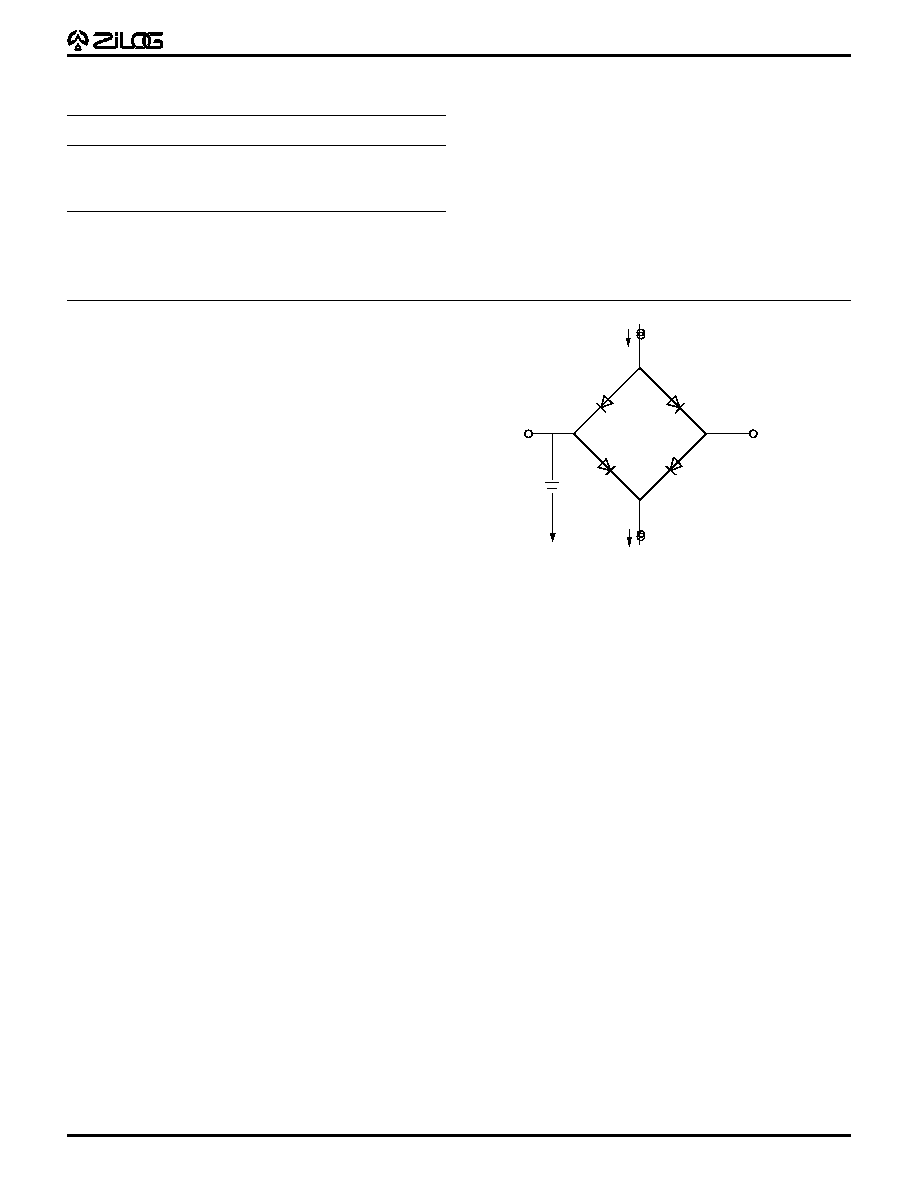
STANDARD TEST CONDITIONS
The characteristics listed below apply for standard test
conditions as noted (Test Load Diagram).
Test Load Diagram
8
Z86C95 DSP
CPS DC-4067-13
DC ELECTRICAL CHARACTERISTICS
V
CC
= 3.3V
±
10%
T
A
= 0
∞
C to +70
∞
C
Typical
Sym
Parameter
Min
Max
at 25
∞
C
Units
Conditions
Max Input Voltage
7
V
I
IN
250
µ
A
V
CH
Clock Input High Voltage
0.8 V
CC
V
CC
V
Driven by External Clock Generator
V
CL
Clock Input Low Voltage
≠0.03
0.1xV
CC
V
Driven by External Clock Generator
V
IH
Input High Voltage
0.6xV
CC
V
CC
V
V
IL
Input Low Voltage
≠0.3
0.2xV
CC
V
V
OH
Output High Voltge
2.0
V
I
OH
= ≠1.0 mA
V
OH
Output High Voltge
V
CC
≠ 100 mV
V
I
OH
= ≠100
µ
A
V
OL
Output Low Voltage
0.4
V
I
OL
= +1.0 mA
V
RH
Reset Input High Voltage
0.8xV
CC
V
CC
V
V
Rl
Reset Input Low Voltage
≠0.03
0.2xV
CC
V
I
IL
Input Leakage
≠2
2
µ
A
Test at 0V, V
CC
I
OL
Output Leakage
≠2
2
µ
A
Test at 0V, V
CC
I
IR
Reset Input Current
≠180
µ
A
V
RL
= 0V
I
CC
Supply Current
50
40
mA
@ 24 MHz [1]
I
CC1
HALT
15
10
mA
HALT Mode V
IN
=OV, V
CC
@ 24 MHz [1]
I
CC2
STOP and Pause Mode
20
6
µ
A
STOP Mode V
IN
=OV, V
CC
[1]
I
ALL
Auto Latch Low Current
≠10
10
5
µ
A
Note:
[1] All inputs driven to 0V, V
CC
and outputs floating.
9
Z86C95 DSP
CPS DC-4067-13
DC ELECTRICAL CHARACTERISTICS
V
CC
= 5.0V
±
10%
T
A
= 0
∞
C to +70
∞
C
Typical
Sym
Parameter
Min
Max
at 25
∞
C
Units
Conditions
Max Input Voltage
7
V
I
IN
250
µ
A
V
CH
Clock Input High Voltage
3.8
V
CC
V
Driven by External Clock Generator
V
CL
Clock Input Low Voltage
≠0.03
0.8
V
Driven by External Clock Generator
V
IH
Input High Voltage
2.0
V
CC
V
V
IL
Input Low Voltage
≠0.3
0.8
V
V
OH
Output High Voltge
2.4
V
I
OH
= ≠2.0 mA
V
OH
Output High Voltge
V
CC
≠ 100mV
V
I
OH
= ≠100
µ
A
V
OL
Output Low Voltage
0.4
V
I
OH
= +2.0 mA
V
RH
Reset Input High Voltage
3.8
V
CC
V
V
Rl
Reset Input Low Voltage
≠0.03
0.8
V
I
IL
Input Leakage
≠2
2
µ
A
Test at 0V, V
CC
I
OL
Output Leakage
≠2
2
µ
A
Test at 0V, V
CC
I
IR
Reset Input Current
≠180
µ
A
V
RL
= 0V
I
CC
Supply Current
82
50
mA
@ 24 MHz [1]
120
70
mA
@ 33 MHz [1]
150
85
mA
@ 40 MHz [1], [2]
I
CC1
HALT
20
13
mA
HALT Mode V
IN
=OV, V
CC
@ 24 MHz [1]
30
20
mA
HALT Mode V
IN
=OV, V
CC
@ 33 MHz [1]
45
30
mA
HALT Mode V
IN
=OV, V
CC
@ 40 MHz [1], [2]
I
CC2
STOP and Pause Mode
20
6
µ
A
STOP Mode V
IN
=OV, V
CC
[1]
I
ALL
Auto Latch Low Current
≠20
20
5
µ
A
Note:
[1] All inputs driven to 0V, V
CC
and outputs floating.
[2] Preliminary values, to be characterized.
10
Z86C95 DSP
CPS DC-4067-13
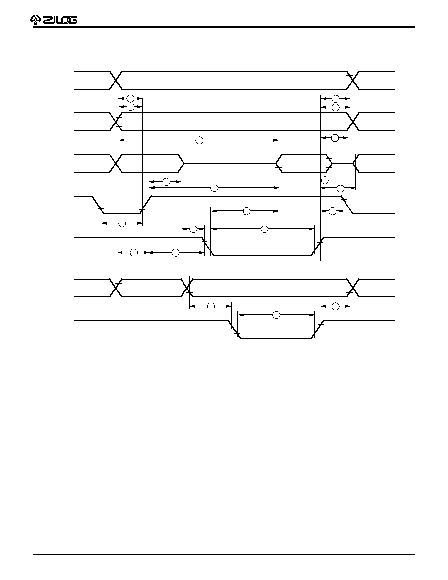
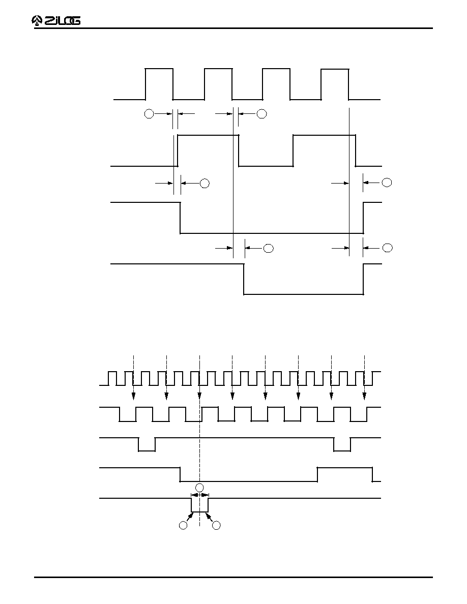
AC CHARACTERISTICS
External I/O or Memory Read/Write Timing Diagram
R/W, /DM
9
12
3
16
20
4
5
8
11
6
17
15
7
14
2
Port 0
Port 1
/AS
/DS
(Read)
Port1
/DS
(Write)
A0 - A7
D0 - D7 IN
D0 - D7 OUT
A0 - A7
13
21
19
10
A0 - A7
A0-A7
1
A8 - A15
External I/O or Memory Read/Write Timing

11
Z86C95 DSP
CPS DC-4067-13
AC CHARACTERISTICS
External I/O or Memory Read and Write; DSR/DSW; WAIT Timing Table
T
A
= 0
∞
C to +70
∞
C
40 MHz**
33 MHz
24 MHz
No
Sym
Parameter
Min
Max
Min
Max
Min
Max
Units
1
TdA(AS)
Address Valid To /AS Rise Delay
8
15
22
ns
2
TdAS(A)
/AS Rise To Address Hold Time
15
20
25
ns
3
TdAS(DI)
/AS Rise Data In Req'd Valid Delay
75
96
130
ns
4
TwAS
/AS Low Width
10
15
28
ns
5
TdAZ(DSR)
Address Float To /DS Fall (Read)
0
0
0
ns
6
TwDSR
/DS (Read) Low Width
60
65
100
ns
7
TwDSW
/DS (Write) Low Width
35
40
65
ns
8
TdDSR(DI)
/DS Fall (Read) To Data Req'd Valid Delay
40
45
80
ns
9
ThDSR(DI)
/DS Rise (Read) to Data In Hold Time
0
0
0
ns
10
TdDS(A)
/DS Rise To Address Active Delay
20
25
40
ns
11
TdDS(AS)
/DS Rise To /AS Delay
16
16
30
ns
12
TdR/W(AS)
R/W To Valid /AS Rise Delay
10
12
26
ns
13
TdDS(R/W)
/DS Rise To R/W Not Valid Delay
12
12
30
ns
14
TdDO(DSW)
Data Out To /DS Fall (Write) Delay
12
12
34
ns
15
ThDSW(DO)
/DS Rise (Write) To Data Out Hold Time
12
12
34
ns
16
TdA(DI)
Address Valid To Data Req'd Valid Delay
90
115
160
ns
17
TdAS(DSR)
/AS Rise To /DS Fall (Read) Delay
20
20
40
ns
19
TdDM(AS)
/DM Valid To /AS Rise Delay
10
10
22
ns
20
TdDS(DM)
/DS Rise To /DM Valid Delay
15
15
35
ns
21
ThDS(A)
/DS Rise To Address Valid Hold Time
15
15
30
ns
22
TdXT(SCR)
XTAL Falling to SCLK Rising
30
35
40
ns
23
TdXT(SCF)
XTAL Falling to SCLK Falling
30
35
40
ns
24
TdXT(DSRF)
XTAL Falling to/DS Read Falling
40
45
50
ns
25
TdXT(DSRR)
XTAL Falling to /DS Read Rising
30
35
45
ns
26
TdXT(DSWF)
XTAL Falling to /DS Write Falling
40
45
50
ns
27
TdXT(DSWF)
XTAL Falling to /DS Write Rising
30
35
45
ns
28
TsW(XT)
Wait Set-up Time
5
5
5
ns
29
ThW(XT)
Wait Hold Time
15
15
15
ns
30
TwW
Wait Width (One Wait Time)
20
20
25
ns
Notes:
When using extended memory timing add 2 TpC.
Timing numbers given are for minimum TpC.
** Preliminary values, to be characterized.
12
Z86C95 DSP
CPS DC-4067-13
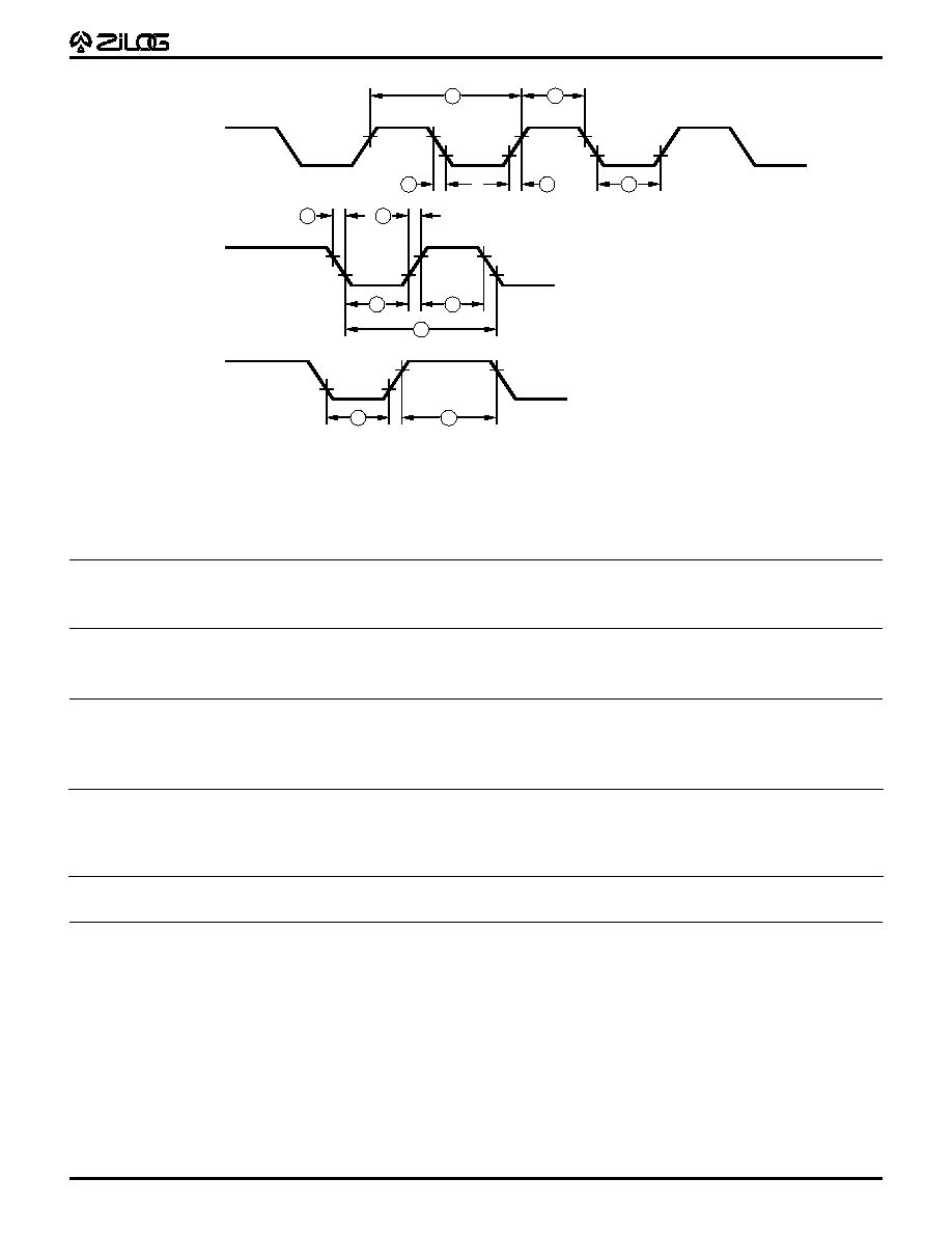
AC CHARACTERISTICS
(Continued)
Timing Diagrams
XTAL1
SCLK
/DS
27
26
25
24
23
22
/DS
(External Clock Drive)
(Read)
(Write)
XTAL/SCLK To DSR and DSW Timing
XTAL1
SCLK
/AS
/DS
/WAIT
T1
T2
TW
TW
TW
T3
T1
30
28
29
XTAL/SCLK To WAIT Timing
13
Z86C95 DSP
CPS DC-4067-13
Clock
1
3
4
8
2
2
3
T IN
IRQ N
6
5
7
7
9
AC CHARACTERISTICS
Additional Timing Table
T
A
= 0
∞
C to +70
∞
C
40 MHz 24 MHz 33 MHz
No
Symbol
Parameter
Min
Max
Min
Max
Min
Max
Units
Notes
1
TpC
Input Clock Period
25
1000
42
1000
30
1000
ns
[1]
2
TrC,TfC
Clock Imput Rise & Fall Times
5
10
5
ns
[1]
3
TwC
Input Clock Width
8
11
10
ns
[1]
4
TwTinL
Timer Input Low Width
75
75
75
ns
[2]
5
TwTinH
Timer Input High Width
3 TpC
3 TpC
3 TpC
[2]
6
TpTin
Timer Input Period
8 TpC
8 TpC
8 TpC
[2]
7
TrTin,TfTin
Timer Input Rise & Fall Times
100
100
100
ns
[2]
8a
TwIL
Interrupt Request Input Low Times
70
70
70
ns
[2,4]
8b
TwIL
Interrupt Request Input Low Times
5 TpC
5 TpC
5 TpC
[2,5]
9
TwIH
Interrupt Request Input High Times
3 TpC
3 TpC
3 TpC
[2,3]
Additional Timing
Notes:
[1] Clock timing references use 3.8V for a logic 1 and 0.8V for a logic 0.
[2] Timing references use 2.0V for a logic 1 and 0.8V for a logic 0.
[3] Interrupt references request via Port 3.
[4] Interrupt request via Port 3 (P33-P31).
[5] Interrupt request via Port 30.
14
Z86C95 DSP
CPS DC-4067-13
AC CHARACTERISTICS
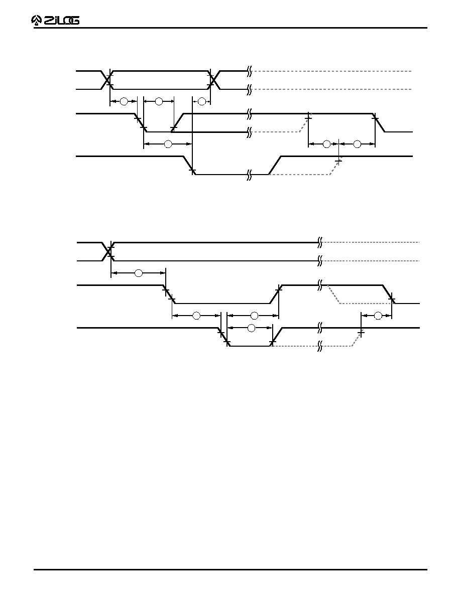
Handshake Timing Diagrams
Data In
1
3
4
5
6
/DAV
(Input)
RDY
(Output)
Next Data In Valid
Delayed RDY
Delayed DAV
Data In Valid
2
Data Out
/DAV
(Output)
RDY
(Input)
Next Data Out Valid
Delayed RDY
Delayed DAV
Data Out Valid
7
8
9
10
11
Input Handshake Timing
Output Handshake Timing
15
Z86C95 DSP
CPS DC-4067-13
AC CHARACTERISTICS
Handshake Timing Table
T
A
= 0
∞
C to +70
∞
C
Data
No
Symbol
Parameter
Min
Max
Units Direction
1
TsDI(DAV)
Data In Setup Time to /DAV
0
ns
In
2
ThDI(DAV)
RDY to Data In Hold Time
0
ns
In
3
TwDAV
/DAV Width
40
ns
In
4
TdDAVIf(RDYf)
/DAV to RDY Delay
70
ns
In
5
TdDAVIr(RDYr)
DAV Rise to RDY Wait Time
40
ns
In
6
TdRDYOr(DAVIf)
RDY Rise to DAV Delay
0
ns
In
7
TdD0(DAV)
Data Out to DAV Delay
TpC
ns
Out
8
TdDAV0f(RDYIf)
/DAV to RDY Delay
0
ns
Out
9
TdRDYIf(DAVOr)
RDY to /DAV Rise Delay
70
ns
Out
10
TwRDY
RDY Width
40
ns
Out
11
TdRDYIr(DAVOf)
RDY Rise to DAV Wait Time
40
ns
Out

16
Z86C95 DSP
CPS DC-4067-13
AC CHARACTERISTICS
(Continued)
A/D Converter Electrical Characteristics
V
CC
= 3.3V
±
10%
Parameter
Minimum
Typical
Maximum
Units
Resolution
8
Bits
Integral non-linearity
0.5
1
LSB
Differential non-linearity
0.5
1
LSB
Zero Error at 25
∞
C
5.0
mV
Supply Range
2.7
3.0
3.3
Volts
Power dissapation, no load
20
40
mW
Clock frequency
24
MHz
Input voltage range
VA
LO
VA
HI
Volts
Conversion time
2
µ
sec
Input capacitance on ANA
25
40
pF
VA
HI
range
VA
LO
+2.5
AV
CC
Volts
VA
LO
range
AN
GND
AV
CC
≠2.5
Volts
VA
HI
-≠VA
LO
2.5
AV
CC
Volts
Notes:
Voltage 2.7V ≠ 3.3V
Temp 0-70
∞
C
D/A Converter Electrical Characteristics
V
CC
= 3.3V
±
10%
Parameter
Minimum
Typical
Maximum
Units
Resolution
8
Bits
Integral non-linearity
0.25
1
LSB
Differential non-linearity
0.25
0.5
LSB
Setting time, 1/2 LSB
1.5
3.0
µ
sec
Zero Error at 25
∞
C
10
20
mV
Full Scale error at 25
∞
C
0.25
0.5
LSB
Supply Range
2.7
3.0
3.3
Volts
Power dissapation, no load
10
mW
Ref Input resistance
2K
4K
10K
Ohms
Output noise voltage
50
µ
Vp-p
VD
HI
range at 3 volts
1.5
1.8
2.1
Volts
VD
LO
range at 3 volts
0.2
0.5
0.8
Volts
VD
HI
≠VD
LO
, at 3 volts
1.3
1.6
1.9
Volts
Capacitive output load, CL
20
pF
Resistive output load, RL
50K
Ohms
Output slew rate
1.0
3.0
V/
µ
sec
Notes:
Voltage 2.7V ≠ 3.3V
Temp 0-70
∞
C
17
Z86C95 DSP
CPS DC-4067-13
A/D Converter Electrical Characteristics
V
CC
= 5.0V
±
10%
Parameter
Minimum
Typical
Maximum
Units
Resolution
8
Bits
Integral non-linearity
0.5
1
LSB
Differential non-linearity
0.5
1
LSB
Zero Error at 25
∞
C
45
mV
Supply Range
4.5
5.0
5.5
Volts
Power dissapation, no load
50
85
mW
Clock frequency
33
MHz
Input voltage range
VA
LO
VA
HI
Volts
Conversion time
2
µ
sec
Input capacitance on ANA
25
40
pF
VA
HI
range
VA
LO
+2.5
AV
CC
Volts
VA
LO
range
AN
GND
AV
CC
≠2.5
Volts
VA
HI
-≠VA
LO
2.5
AV
CC
Volts
Notes:
Voltage 4.5V ≠5.5V
Temp 0-70
∞
C
D/A Converter Electrical Characteristics
V
CC
= 5.0V
±
10%
Parameter
Minimum
Typical
Maximum
Units
Resolution
8
Bits
Integral non-linearity
0.25
1
LSB
Differential non-linearity
0.25
0.5
LSB
Setting time, 1/2 LSB
1.5
3.0
µ
sec
Zero Error at 25
∞
C
10
20
mV
Full Scale error at 25
∞
C
1
2
% FSR
Supply Range
4.5
5.0
5.5
Volts
Power dissapation, no load
50
85
mW
Ref Input resistance
2K
4K
10K
Ohms
Output noise voltage
50
µ
Vp-p
VD
HI
range at 3 volts
2.6
3.5
Volts
VD
LO
range at 5V volts
0.8
1.7
Volts
VD
HI
≠VD
LO
, at 5V volts
0.9
2.7
Volts
Capacitive output load, CL
30
pF
Resistive output load, RL
20K*
Ohms
Output slew rate
1.0
3.0
V/
µ
sec
Notes:
Voltage 4.5V - 5.5V
Temp 0-70
∞
C
* 100K for 24 MHz device.
18
Z86C95 DSP
CPS DC-4067-13
© 1994 by Zilog, Inc. All rights reserved. No part of this document
may be copied or reproduced in any form or by any means
without the prior written consent of Zilog, Inc. The information in
this document is subject to change without notice. Devices sold
by Zilog, Inc. are covered by warranty and patent indemnification
provisions appearing in Zilog, Inc. Terms and Conditions of Sale
only. Zilog, Inc. makes no warranty, express, statutory, implied or
by description, regarding the information set forth herein or
regarding the freedom of the described devices from intellectual
property infringement. Zilog, Inc. makes no warranty of mer-
chantability or fitness for any purpose. Zilog, Inc. shall not be
responsible for any errors that may appear in this document.
Zilog, Inc. makes no commitment to update or keep current the
information contained in this document.
Zilog's products are not authorized for use as critical compo-
nents in life support devices or systems unless a specific written
agreement pertaining to such intended use is executed between
the customer and Zilog prior to use. Life support devices or
systems are those which are intended for surgical implantation
into the body, or which sustains life whose failure to perform,
when properly used in accordance with instructions for use
provided in the labeling, can be reasonably expected to result in
significant injury to the user.
Zilog, Inc. 210 East Hacienda Ave.
Campbell, CA 95008-6600
Telephone (408) 370-8000
Telex 910-338-7621
FAX 408 370-8056