
ZiLOG Worldwide Headquarters ∑ 532 Race Street ∑ San Jose, CA 95126-3432
Telephone: 408.558.8500 ∑ Fax: 408.558.8300 ∑
www.ZiLOG.com
Preliminary Product Specification
PS008904-1003
Z86D86
28-Pin Low-Voltage OTP
Microcontroller

P R E L I M I N A R Y
PS008904-1003
This publication is subject to replacement by a later edition. To determine whether a later edition
exists, or to request copies of publications, contact:
ZiLOG Worldwide Headquarters
532 Race Street
San Jose, CA 95126-3432
Telephone: 408.558.8500
Fax: 408.558.8300
www.ZiLOG.com
ZiLOG is a registered trademark of ZiLOG Inc. in the United States and in other countries. All other products and/or
service names mentioned herein may be trademarks of the companies with which they are associated.
Document Disclaimer
© 2003 by ZiLOG, Inc. All rights reserved. Information in this publication concerning the devices, applications, or
technology described is intended to suggest possible uses and may be superseded. ZiLOG, INC. DOES NOT
ASSUME LIABILITY FOR OR PROVIDE A REPRESENTATION OF ACCURACY OF THE INFORMATION, DEVICES,
OR TECHNOLOGY DESCRIBED IN THIS DOCUMENT. ZiLOG ALSO DOES NOT ASSUME LIABILITY FOR
INTELLECTUAL PROPERTY INFRINGEMENT RELATED IN ANY MANNER TO USE OF INFORMATION, DEVICES,
OR TECHNOLOGY DESCRIBED HEREIN OR OTHERWISE. Except with the express written approval ZiLOG, use of
information, devices, or technology as critical components of life support systems is not authorized. No licenses or
other rights are conveyed, implicitly or otherwise, by this document under any intellectual property rights.

Z86D86
28-Pin Low-Voltage OTP Microcontroller
PS008904-1003
P R E L I M I N A R Y
iii
Table of Contents
Features . . . . . . . . . . . . . . . . . . . . . . . . . . . . . . . . . . . . . . . . . . . . . . . . . . . . . . . 1
General Description . . . . . . . . . . . . . . . . . . . . . . . . . . . . . . . . . . . . . . . . . . . . . . . 2
Pin Description . . . . . . . . . . . . . . . . . . . . . . . . . . . . . . . . . . . . . . . . . . . . . . . . . . 5
Absolute Maximum Ratings . . . . . . . . . . . . . . . . . . . . . . . . . . . . . . . . . . . . . . . . . 6
Standard Test Conditions . . . . . . . . . . . . . . . . . . . . . . . . . . . . . . . . . . . . . . . . . . 7
Capacitance . . . . . . . . . . . . . . . . . . . . . . . . . . . . . . . . . . . . . . . . . . . . . . . . . . . . 7
DC Characteristics . . . . . . . . . . . . . . . . . . . . . . . . . . . . . . . . . . . . . . . . . . . . . . . 8
AC Characteristics . . . . . . . . . . . . . . . . . . . . . . . . . . . . . . . . . . . . . . . . . . . . . . . 10
Pin Functions (Standard Mode) . . . . . . . . . . . . . . . . . . . . . . . . . . . . . . . . . . . . . 12
XTAL1 Crystal 1 (Time-Based Input) . . . . . . . . . . . . . . . . . . . . . . . . . . . . . 12
XTAL2 Crystal 2 (Time-Based Output) . . . . . . . . . . . . . . . . . . . . . . . . . . . . 12
Port 0 (P07≠P00) . . . . . . . . . . . . . . . . . . . . . . . . . . . . . . . . . . . . . . . . . . . . . 12
Port 2 (P27≠P20) . . . . . . . . . . . . . . . . . . . . . . . . . . . . . . . . . . . . . . . . . . . . . 13
Port 3 (P37≠P31) . . . . . . . . . . . . . . . . . . . . . . . . . . . . . . . . . . . . . . . . . . . . . 14
Comparator Inputs . . . . . . . . . . . . . . . . . . . . . . . . . . . . . . . . . . . . . . . . . . . . 16
Comparator Outputs . . . . . . . . . . . . . . . . . . . . . . . . . . . . . . . . . . . . . . . . . . 16
Functional Description . . . . . . . . . . . . . . . . . . . . . . . . . . . . . . . . . . . . . . . . . . . . 18
Program Memory . . . . . . . . . . . . . . . . . . . . . . . . . . . . . . . . . . . . . . . . . . . . . 18
RAM . . . . . . . . . . . . . . . . . . . . . . . . . . . . . . . . . . . . . . . . . . . . . . . . . . . . . . 18
Expanded Register File . . . . . . . . . . . . . . . . . . . . . . . . . . . . . . . . . . . . . . . . 18
Register File . . . . . . . . . . . . . . . . . . . . . . . . . . . . . . . . . . . . . . . . . . . . . . . . 32
Stack . . . . . . . . . . . . . . . . . . . . . . . . . . . . . . . . . . . . . . . . . . . . . . . . . . . . . . 33
Counter/Timer Registers . . . . . . . . . . . . . . . . . . . . . . . . . . . . . . . . . . . . . . . 34
Counter/Timer Functional Blocks . . . . . . . . . . . . . . . . . . . . . . . . . . . . . . . . 43
Interrupts . . . . . . . . . . . . . . . . . . . . . . . . . . . . . . . . . . . . . . . . . . . . . . . . . . . 54
Clock . . . . . . . . . . . . . . . . . . . . . . . . . . . . . . . . . . . . . . . . . . . . . . . . . . . . . . 56
Power-On Reset (POR) . . . . . . . . . . . . . . . . . . . . . . . . . . . . . . . . . . . . . . . . 57
HALT . . . . . . . . . . . . . . . . . . . . . . . . . . . . . . . . . . . . . . . . . . . . . . . . . . . . . . 58
STOP . . . . . . . . . . . . . . . . . . . . . . . . . . . . . . . . . . . . . . . . . . . . . . . . . . . . . . 58
Port Configuration Register (PCON) . . . . . . . . . . . . . . . . . . . . . . . . . . . . . . 59
Stop-Mode Recovery Register (SMR) . . . . . . . . . . . . . . . . . . . . . . . . . . . . . 59
Stop-Mode Recovery Register 2 (SMR2) . . . . . . . . . . . . . . . . . . . . . . . . . . 64
Watch-Dog Timer Mode Register (WDTMR) . . . . . . . . . . . . . . . . . . . . . . . . 65
Mask Selectable Options . . . . . . . . . . . . . . . . . . . . . . . . . . . . . . . . . . . . . . . 68
Low Voltage/Standby . . . . . . . . . . . . . . . . . . . . . . . . . . . . . . . . . . . . . . . . . 68

Z86D86
28-Pin Low-Voltage OTP Microcontroller
PS008904-1003
P R E L I M I N A R Y
iv
Low Battery Detection and Flag . . . . . . . . . . . . . . . . . . . . . . . . . . . . . . . . . 68
Ordering Information . . . . . . . . . . . . . . . . . . . . . . . . . . . . . . . . . . . . . . . . . . . . . 69
Z86D86 8.0 MHz . . . . . . . . . . . . . . . . . . . . . . . . . . . . . . . . . . . . . . . . . . . . . 70
Codes . . . . . . . . . . . . . . . . . . . . . . . . . . . . . . . . . . . . . . . . . . . . . . . . . . . . . 71
Precharacterization Product . . . . . . . . . . . . . . . . . . . . . . . . . . . . . . . . . . . . 71
Customer Feedback Form . . . . . . . . . . . . . . . . . . . . . . . . . . . . . . . . . . . . . . . . . 72
Z86D86 28-Pin Low-Voltage OTP Microcontroller . . . . . . . . . . . . . . . . . . . 72
Customer Information . . . . . . . . . . . . . . . . . . . . . . . . . . . . . . . . . . . . . . . . . 72
Product Information . . . . . . . . . . . . . . . . . . . . . . . . . . . . . . . . . . . . . . . . . . . 72
Return Information . . . . . . . . . . . . . . . . . . . . . . . . . . . . . . . . . . . . . . . . . . . . 72
Problem Description or Suggestion . . . . . . . . . . . . . . . . . . . . . . . . . . . . . . . 72

Z86D86
28-Pin Low-Voltage OTP Microcontroller
PS008904-1003
P R E L I M I N A R Y
v
List of Figures
Figure 1. Counter/Timers Diagram . . . . . . . . . . . . . . . . . . . . . . . . . . . . . . . . . . 3
Figure 2. Functional Block Diagram . . . . . . . . . . . . . . . . . . . . . . . . . . . . . . . . . 4
Figure 3. 28-Pin DIP/SOIC Pin Assignment . . . . . . . . . . . . . . . . . . . . . . . . . . . 5
Figure 4. Test Load Diagram . . . . . . . . . . . . . . . . . . . . . . . . . . . . . . . . . . . . . . 7
Figure 5. Timing Diagram . . . . . . . . . . . . . . . . . . . . . . . . . . . . . . . . . . . . . . . . 10
Figure 6. Port 0 Configuration . . . . . . . . . . . . . . . . . . . . . . . . . . . . . . . . . . . . . 13
Figure 7. Port 2 Configuration . . . . . . . . . . . . . . . . . . . . . . . . . . . . . . . . . . . . . 14
Figure 8. Port 3 Configuration . . . . . . . . . . . . . . . . . . . . . . . . . . . . . . . . . . . . . 15
Figure 9. Port 3 Counter/Timer Output Configuration . . . . . . . . . . . . . . . . . . . 17
Figure 10. Program Memory Map (32K ROM) . . . . . . . . . . . . . . . . . . . . . . . . . 18
Figure 11. Expanded Register File Architecture . . . . . . . . . . . . . . . . . . . . . . . . 20
Figure 12. Register Pointer Register . . . . . . . . . . . . . . . . . . . . . . . . . . . . . . . . 21
Figure 13. TC8 Control Register--(0D) OH: Read/Write
Except Where Noted . . . . . . . . . . . . . . . . . . . . . . . . . . . . . . . . . . . . 21
Figure 14. T8 and T16 Common Control Functions--(0D) 1H:
Read/Write . . . . . . . . . . . . . . . . . . . . . . . . . . . . . . . . . . . . . . . . . . . . 22
Figure 15. T16 Control Register--(0D) 2H: Read/Write
Except Where Noted . . . . . . . . . . . . . . . . . . . . . . . . . . . . . . . . . . . . 23
Figure 16. Low Battery Detection . . . . . . . . . . . . . . . . . . . . . . . . . . . . . . . . . . . 24
Figure 17. Stop-Mode Recovery Register--(0F) 0BH:
D6≠D0 = Write Only, D7 = Read Only . . . . . . . . . . . . . . . . . . . . . . . 25
Figure 18. Stop-Mode Recovery Register 2--(0F) 0DH: D2≠D4,
D6 Write Only . . . . . . . . . . . . . . . . . . . . . . . . . . . . . . . . . . . . . . . . . 26
Figure 19. Watch-Dog Timer Register--(0F) 0FH: Write Only . . . . . . . . . . . . . 27
Figure 20. Port Configuration Register (PCON)--(0F) 0H: Write Only . . . . . . . 27
Figure 21. Port 2 Mode Register--F6H: Write Only . . . . . . . . . . . . . . . . . . . . . 28
Figure 22. Port 3 Mode Register--F7H: Write Only . . . . . . . . . . . . . . . . . . . . . 28
Figure 23. Port 0 and 1 Mode Register--F8H: Write Only . . . . . . . . . . . . . . . . 29
Figure 24. Interrupt Priority Register--F9H: Write Only . . . . . . . . . . . . . . . . . . 30
Figure 25. Interrupt Request Register--FAH: Read/Write . . . . . . . . . . . . . . . . 30
Figure 26. Interrupt Mask Register--FBH: Read/Write . . . . . . . . . . . . . . . . . . . 31
Figure 27. Flag Register--FCH: Read/Write . . . . . . . . . . . . . . . . . . . . . . . . . . 31
Figure 28. Register Pointer--FDH: Read/Write . . . . . . . . . . . . . . . . . . . . . . . . 32
Figure 29. Stack Pointer High--FEH: Read/Write . . . . . . . . . . . . . . . . . . . . . . 32
Figure 30. Stack Pointer Low--FFH: Read/Write . . . . . . . . . . . . . . . . . . . . . . . 32

Z86D86
28-Pin Low-Voltage OTP Microcontroller
PS008904-1003
P R E L I M I N A R Y
vi
Figure 31. Register Pointer . . . . . . . . . . . . . . . . . . . . . . . . . . . . . . . . . . . . . . . . 33
Figure 32. Glitch Filter Circuitry . . . . . . . . . . . . . . . . . . . . . . . . . . . . . . . . . . . . 44
Figure 33. 8-Bit Counter/Timer Circuits . . . . . . . . . . . . . . . . . . . . . . . . . . . . . . 44
Figure 34. Transmit Mode Flowchart . . . . . . . . . . . . . . . . . . . . . . . . . . . . . . . . 46
Figure 35. T8_OUT in Single-Pass Mode . . . . . . . . . . . . . . . . . . . . . . . . . . . . . 47
Figure 36. T8_OUT in Modulo-N Mode . . . . . . . . . . . . . . . . . . . . . . . . . . . . . . 47
Figure 37. Demodulation Mode Count Capture Flowchart . . . . . . . . . . . . . . . . 48
Figure 38. Demodulation Mode Flowchart . . . . . . . . . . . . . . . . . . . . . . . . . . . . 49
Figure 39. 16-Bit Counter/Timer Circuits . . . . . . . . . . . . . . . . . . . . . . . . . . . . . 50
Figure 40. T16_OUT in Single-Pass Mode . . . . . . . . . . . . . . . . . . . . . . . . . . . . 51
Figure 41. T16_OUT in Modulo-N Mode . . . . . . . . . . . . . . . . . . . . . . . . . . . . . 51
Figure 42. Ping-Pong Mode . . . . . . . . . . . . . . . . . . . . . . . . . . . . . . . . . . . . . . . 53
Figure 43. Output Circuit . . . . . . . . . . . . . . . . . . . . . . . . . . . . . . . . . . . . . . . . . . 54
Figure 44. Interrupt Block Diagram . . . . . . . . . . . . . . . . . . . . . . . . . . . . . . . . . . 55
Figure 45. Oscillator Configuration . . . . . . . . . . . . . . . . . . . . . . . . . . . . . . . . . . 57
Figure 46. Port Configuration Register (PCON)--Write Only . . . . . . . . . . . . . . 59
Figure 47. Stop-Mode Recovery Register . . . . . . . . . . . . . . . . . . . . . . . . . . . . 60
Figure 48. SCLK Circuit . . . . . . . . . . . . . . . . . . . . . . . . . . . . . . . . . . . . . . . . . . . 60
Figure 49. Stop-Mode Recovery Source . . . . . . . . . . . . . . . . . . . . . . . . . . . . . 62
Figure 50. Stop-Mode Recovery Register 2--(0F) DH:D2≠D4,
D6 Write Only . . . . . . . . . . . . . . . . . . . . . . . . . . . . . . . . . . . . . . . . . 64
Figure 51. Watch-Dog Timer Mode Register--Write Only . . . . . . . . . . . . . . . . 66
Figure 52. Resets and WDT . . . . . . . . . . . . . . . . . . . . . . . . . . . . . . . . . . . . . . . 67
Figure 53. 28-Pin SOIC Package Diagram . . . . . . . . . . . . . . . . . . . . . . . . . . . . 69
Figure 54. 28-Pin DIP Package Diagram . . . . . . . . . . . . . . . . . . . . . . . . . . . . . 70
Figure 55. Ordering Codes Example . . . . . . . . . . . . . . . . . . . . . . . . . . . . . . . . 71

Z86D86
28-Pin Low-Voltage OTP Microcontroller
PS008904-1003
P R E L I M I N A R Y
vii
List of Tables
Table 1.
Z86D86 Features . . . . . . . . . . . . . . . . . . . . . . . . . . . . . . . . . . . . . . . . 1
Table 2.
28-Pin DIP and SOIC Pin Identification . . . . . . . . . . . . . . . . . . . . . . . 5
Table 3.
Absolute Maximum Ratings . . . . . . . . . . . . . . . . . . . . . . . . . . . . . . . . 6
Table 4.
Capacitance . . . . . . . . . . . . . . . . . . . . . . . . . . . . . . . . . . . . . . . . . . . . 7
Table 5.
DC Characteristics . . . . . . . . . . . . . . . . . . . . . . . . . . . . . . . . . . . . . . 8
Table 6.
AC Characteristics . . . . . . . . . . . . . . . . . . . . . . . . . . . . . . . . . . . . . . 11
Table 7.
Pin Assignments . . . . . . . . . . . . . . . . . . . . . . . . . . . . . . . . . . . . . . . 16
Table 8.
Expanded Register Group D . . . . . . . . . . . . . . . . . . . . . . . . . . . . . . 34
Table 9.
LBD(D)0C--Low Battery Detection Register . . . . . . . . . . . . . . . . . . 35
Table 10. HI8(D)0Bh . . . . . . . . . . . . . . . . . . . . . . . . . . . . . . . . . . . . . . . . . . . . 35
Table 11. L08(D)0Ah . . . . . . . . . . . . . . . . . . . . . . . . . . . . . . . . . . . . . . . . . . . . 35
Table 12. HI16(D)09h . . . . . . . . . . . . . . . . . . . . . . . . . . . . . . . . . . . . . . . . . . . 36
Table 13. L016(D)08h . . . . . . . . . . . . . . . . . . . . . . . . . . . . . . . . . . . . . . . . . . . 36
Table 14. TC16H(D)07h . . . . . . . . . . . . . . . . . . . . . . . . . . . . . . . . . . . . . . . . . 36
Table 15. TC16L(D)06h . . . . . . . . . . . . . . . . . . . . . . . . . . . . . . . . . . . . . . . . . . 36
Table 16. TC8H(D)05h . . . . . . . . . . . . . . . . . . . . . . . . . . . . . . . . . . . . . . . . . . 37
Table 17. TC8L(D)04h . . . . . . . . . . . . . . . . . . . . . . . . . . . . . . . . . . . . . . . . . . . 37
Table 18. CTR0 (D)00 Counter/Timer8 Control Register . . . . . . . . . . . . . . . . 37
Table 19. CTR1(D)01h Register . . . . . . . . . . . . . . . . . . . . . . . . . . . . . . . . . . . 39
Table 20. CTR2 (D)02h: Counter/Timer16 Control Register . . . . . . . . . . . . . . 42
Table 21. Interrupt Types, Sources, and Vectors . . . . . . . . . . . . . . . . . . . . . . 55
Table 22. IRQ Register. . . . . . . . . . . . . . . . . . . . . . . . . . . . . . . . . . . . . . . . . . . 56
Table 23. Stop-Mode Recovery Source . . . . . . . . . . . . . . . . . . . . . . . . . . . . . 63
Table 24. SMR2(F)0Dh: Stop-Mode Recovery Register 2 . . . . . . . . . . . . . . . 65
Table 25. WDT Time Select . . . . . . . . . . . . . . . . . . . . . . . . . . . . . . . . . . . . . . 66
Table 26. Mask Selectable Options . . . . . . . . . . . . . . . . . . . . . . . . . . . . . . . . . 68

Z86D86
28-Pin Low-Voltage OTP Microcontroller
PS008904-1003
P R E L I M I N A R Y
1
Features
Table 1 shows some of the features of the Z86D86 microcontroller.
∑
Low Power Consumption≠40 mW (Typical)
∑
Three Standby Modes
≠ STOP--2 µA
≠ HALT--0.8 mA
≠ Low Voltage
∑
Special Architecture to Automate Both Generation and Reception of Complex
Pulses or Signals:
≠ One Programmable 8-Bit Counter/Timer with Two Capture Registers and
Two Load Registers
≠ One Programmable 16-Bit Counter/Timer with One 16-Bit Capture
Register Pair and One 16-Bit Load Register Pair
≠ Programmable Input Glitch Filter for Pulse Reception
∑
Six Priority Interrupts
≠ Three External
≠ Two Assigned to Counter/Timers
≠ One Low Battery Detection Interrupt
∑
Low Battery Detection with Flag
∑
Programmable Watch-Dog/Power-On Reset Circuits
∑
Two Independent Comparators with Programmable Interrupt Polarity
∑
Mask Selectable 200
±
50% K
Transistor Pull-Ups on Ports 0, 2.
∑
Programmable OTP Options:
≠ Oscillator Selection: RC Oscillator vs. Crystal or Other Clock Source
Table 1. Z86D86 Features
Device
ROM (KB) RAM* (Bytes)
I/O Lines
Voltage Range
Z86D86
32
237
23
2.3 V to 5.5 V
Note: *General purpose

Z86D86
28-Pin Low-Voltage OTP Microcontroller
PS008904-1003
P R E L I M I N A R Y
2
≠ Oscillator Operational Mode: Normal High Frequency Operation Enabled
or 32 KHz Operation Enabled
≠ Port 0: 0≠3 Pull-Ups
≠ Port 0: 4≠7 Pull-Ups
≠ Port 2: 0≠7 Pull-Ups
≠ Port 0: 0≠3 Mouse Mode: Normal Mode (.5V
DD
Input Threshold) vs.
Mouse Mode (.4V
DD
Input Threshold)
∑
Port 3 does not feature the pull-up option.
General Description
The Z86D86 is a 28-pin one-time programmable (OTP) infrared (IR) microcontrol-
ler. Based on a single-chip Z8 microcontroller (MCU) design, the Z86D86 features
237 bytes of general-purpose RAM and 32 KB of OTP ROM. ZiLOG's CMOS
microcontrollers offer fast executing, efficient use of memory, sophisticated inter-
rupts, input/output bit-manipulation capabilities, automated pulse generation/
reception, and internal key-scan pull-up transistors.
The Z86L825 architecture is based on ZiLOG's 8-bit microcontroller core, featur-
ing an Expanded Register File to allow access to register-mapped peripherals, I/O
circuits, and powerful counter/timer circuitry. The Z8 offers a flexible I/O scheme,
an efficient register and address space structure, and a number of ancillary fea-
tures that are useful in many consumer, automotive, computer peripheral, and bat-
ter-operated hand-held applications.
There are three basic address spaces available to support a wide range of config-
urations: program memory, register file, and Expanded Register File. The register
file consists of 256 bytes of RAM. It includes 4 I/O port registers, 16 control and
status registers, and 236 general-purpose registers. (Register FEh (SPH) can be
used as a general-purpose register.) The Expanded Register File consists of two
additional register groups (F and D).
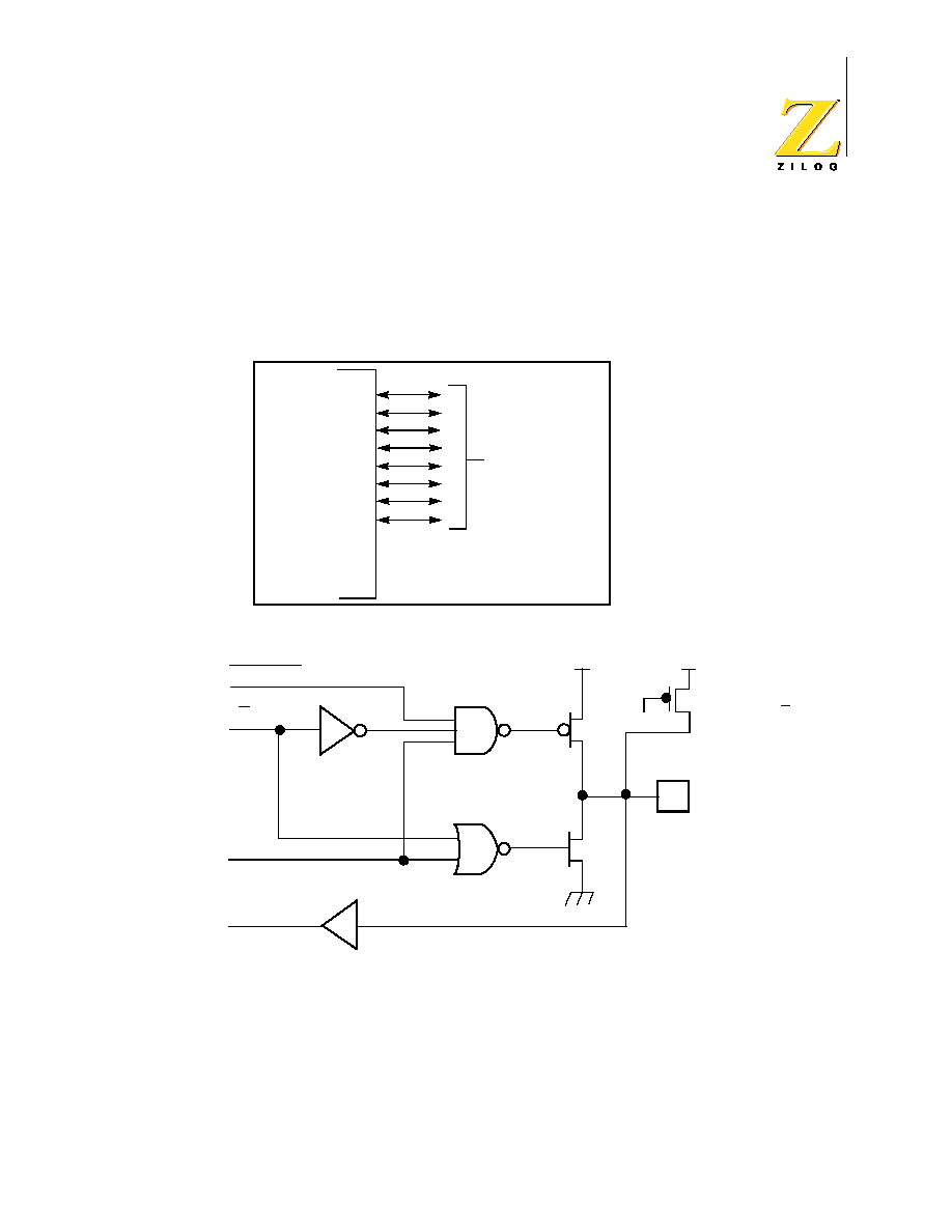
The Z86D86 offers a new intelligent counter/timer architecture with 8-bit and 16-
bit counter/timers (Figure 1). Also included are a large number of user-selectable
modes and two on-board comparators to process analog signals with separate
reference voltages (Figure 9 on page 17).
Z86D86
28-Pin Low-Voltage OTP Microcontroller
PS008904-1003
P R E L I M I N A R Y
3
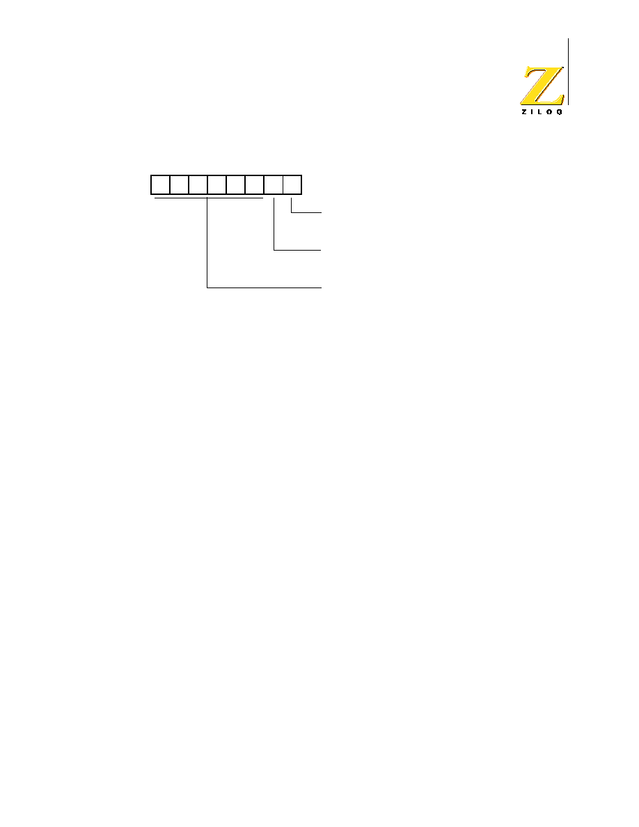
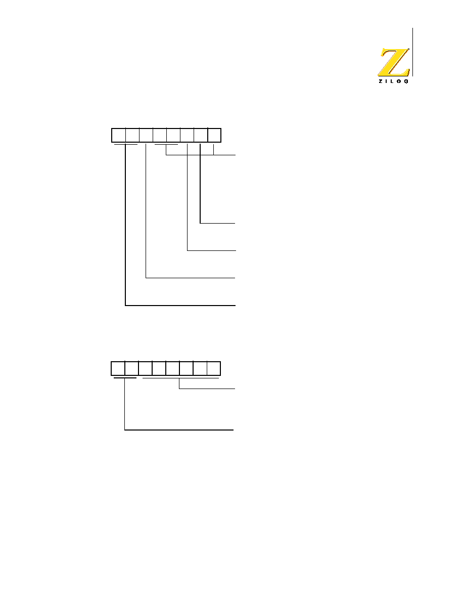
Figure 1. Counter/Timers Diagram
All signals with an overline, " ", are active Low. For example,
B/W, in which WORD is active Low, and B/W, in which BYTE is
active Low.
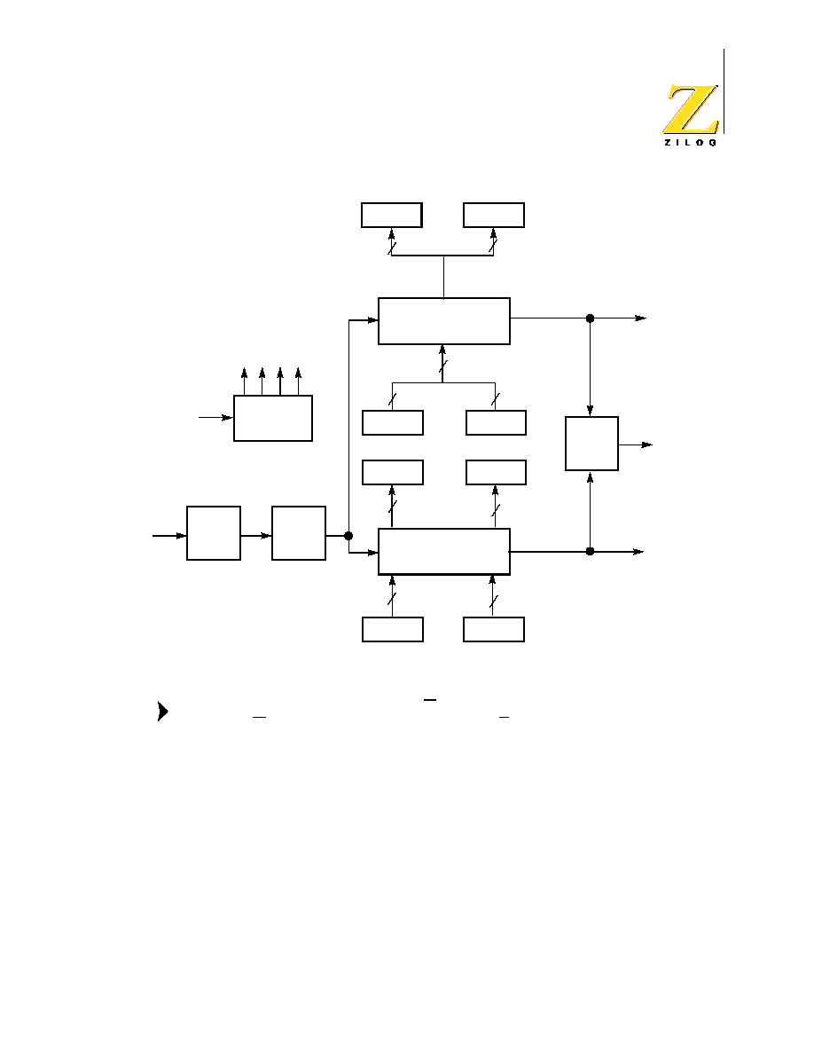
Figure 2 shows the functional block diagram.
HI 16
Lo 16
8
8
16-Bit
T 16
16
Timer 16
1 2 4 8
SCLK
Clock
Divider
8
8
TC16H
TC16L
And/Or
Logic
Timer 8/16
Input
Glitch
Filter
Edge
Detect
Circuit
8-Bit
T8
8
8
TC8H
TC8L
Timer 8
8
8
HI8
LO8
Note:

Z86D86
28-Pin Low-Voltage OTP Microcontroller
PS008904-1003
P R E L I M I N A R Y
4
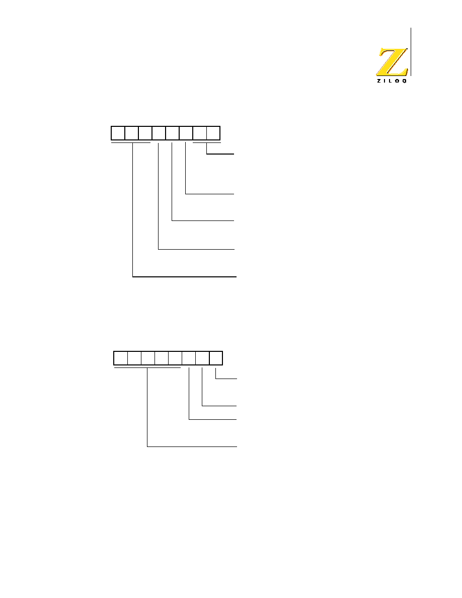
Figure 2. Functional Block Diagram
P00
P01
P02
P03
P04
P05
P06
P07
4
4
Port 0
P20
P21
P22
P23
P24
P25
P26
P27
Port 2
I/O Bit
Programmable
Counter/Timer 8
8-Bit
Expanded
Register
File
OTP or EPROM
32K x 8
Internal
Address Bus
Register File
256 x 8-Bit
Machine
Timing
and
Instruction
Control
Counter/Timer 16
16-Bit
Pref1
P31
P32
P33
P34
P35
P36
P37
Internal
Z8 Core
Expanded
Register Bus
Power
XTAL
V
DD
V
SS
Register Bus
Port 3
Data Bus
I/O Nibble
Programmable

Z86D86
28-Pin Low-Voltage OTP Microcontroller
PS008904-1003
P R E L I M I N A R Y
5
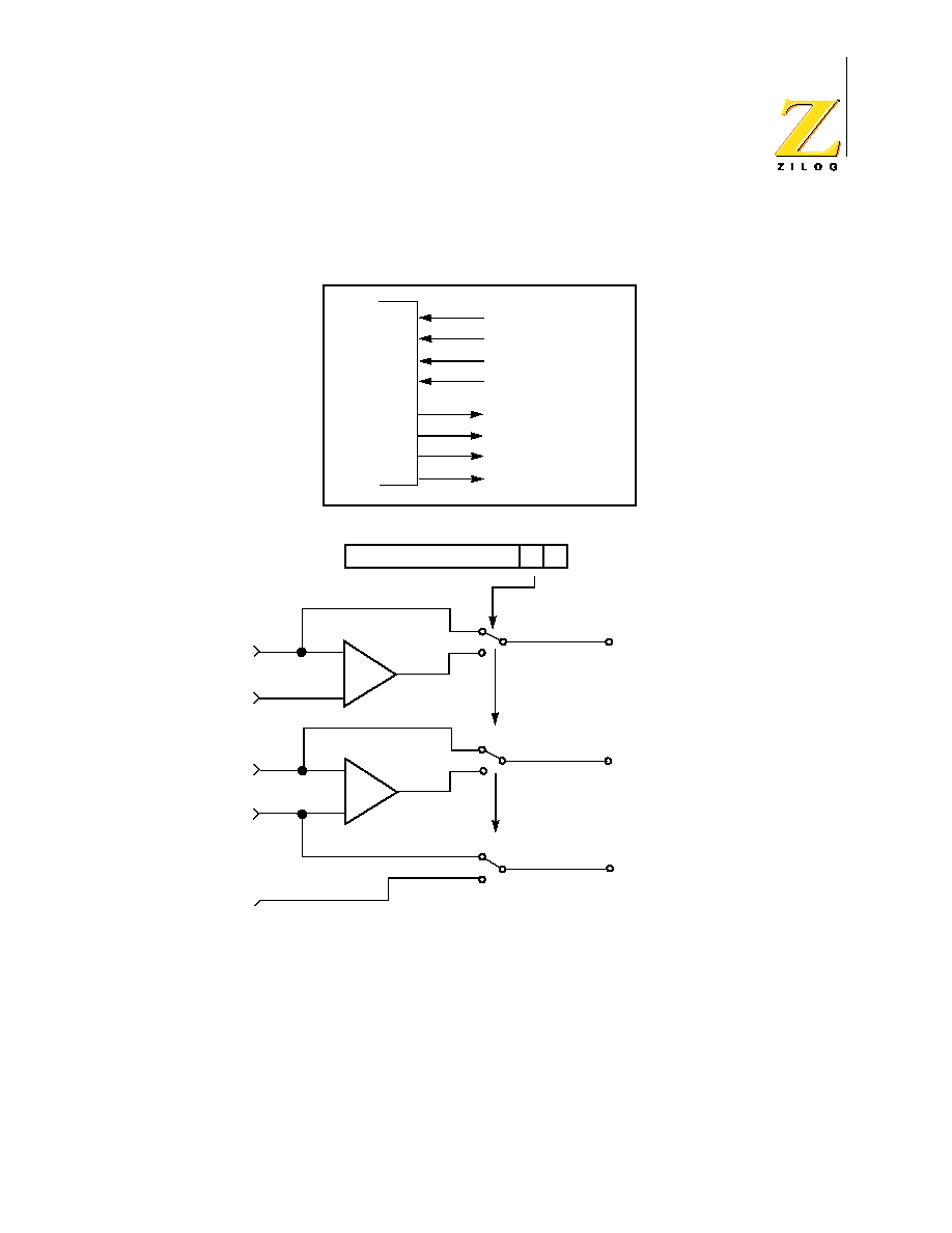
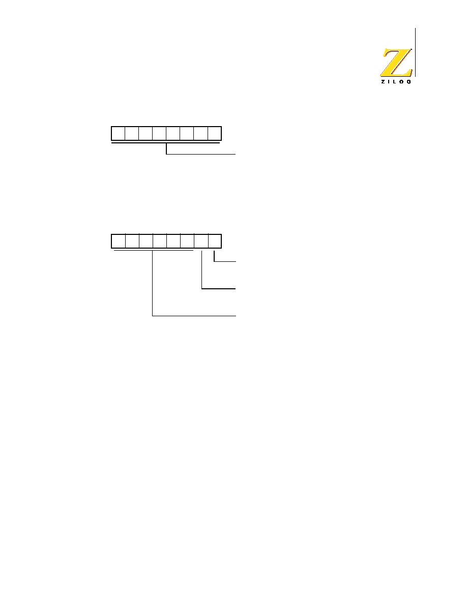
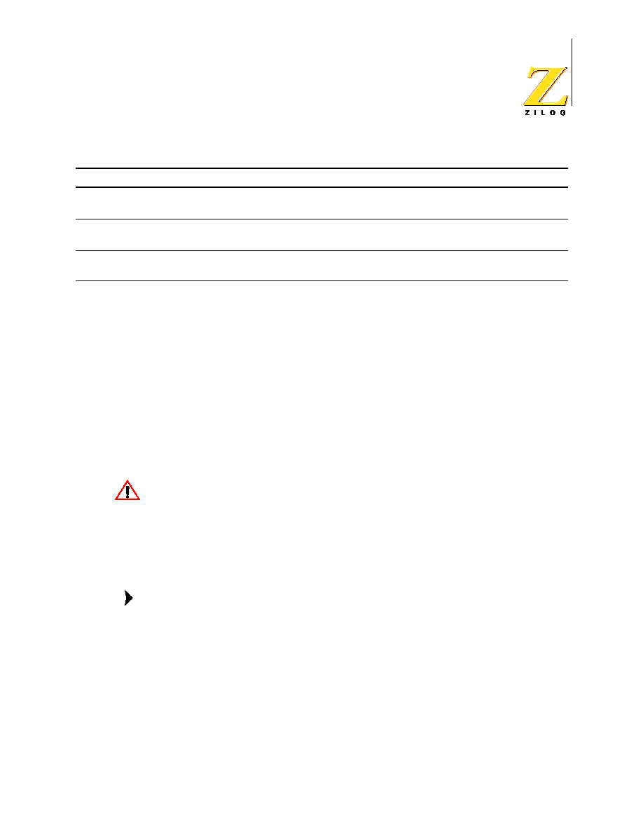
Pin Description
Figure 3 shows the pin assignment for the 28-pin dual in-line package (DIP)/small
outline integrated circuit (SOIC). Table 2 identifies the pins.
Figure 3. 28-Pin DIP/SOIC Pin Assignment
Table 2. 28-Pin DIP and SOIC Pin Identification
28-Pin DIP and SOIC Standard Mode
Direction
Description
19
P00
Input/Output
Port 0 is nibble programmable.
20
P01
Input/Output
Port 0≠3 can be configured as a
21
P02
Input/Output
mouse/trackball input.
23
P03
Input/Output
4
P04
Input/Output
5
P05
Input/Output
6
P06
Input/Output
7
P07
Input/Output
24
P20
Input/Output
Port 2 pins are individually
25
P21
Input/Output
configurable as input or output.
26
P22
Input/Output
27
P23
Input/Output
28
P24
Input/Output
1
P25
Input/Output
2
P26
Input/Output
3
P27
Input/Output
P24
P23
P22
P21
P20
P03
V
SS
P02
P01
P00
Pref1
P36
P37
P35
P25
P26
P27
P04
P05
P06
P07
V
DD
XTAL2
XTAL1
P31
P32
P33
P34
1
14
28
15
Z86D86
DIP/SOIC

Z86D86
28-Pin Low-Voltage OTP Microcontroller
PS008904-1003
P R E L I M I N A R Y
6
Absolute Maximum Ratings
Table 3 lists the absolute maximum ratings for the Z86D86 microcontroller.
Stresses greater than those listed under Absolute Maximum Ratings may cause
permanent damage to the device. This rating is a stress rating only. Functional
operation of the device at any condition above those indicated in the operational
sections of these specifications is not implied. Exposure to absolute maximum rat-
ing conditions for an extended period may affect device reliability.
18
Pref1
Input
Analog ref input (must be pulled high
externally, if not used)
11
P31
Input
IRQ2/modulator input
12
P32
Input
IRQ0
13
P33
Input
IRQ1
14
P34
Output
T8 output
15
P35
Output
T16 output
17
P36
Output
T8/T16 output
16
P37
Output
10
XTAL1
Input
Crystal, oscillator clock
9
XTAL2
Output
Crystal, oscillator clock
8
V
DD
Power supply
22
V
SS
Ground
Table 3. Absolute Maximum Ratings
Symbol
Description
Min
Max
Units
V
MAX
Supply Voltage (*)
≠0.3
+7.0
V
T
STG
Storage Temperature
≠65∞
+150∞
C
T
A
Oper. Ambient Temperature
0∞
70∞
C
Notes:
* Voltage on all pins with respect to GND
Table 2. 28-Pin DIP and SOIC Pin Identification (Continued)
28-Pin DIP and SOIC Standard Mode
Direction
Description
Z86D86
28-Pin Low-Voltage OTP Microcontroller
PS008904-1003
P R E L I M I N A R Y
7
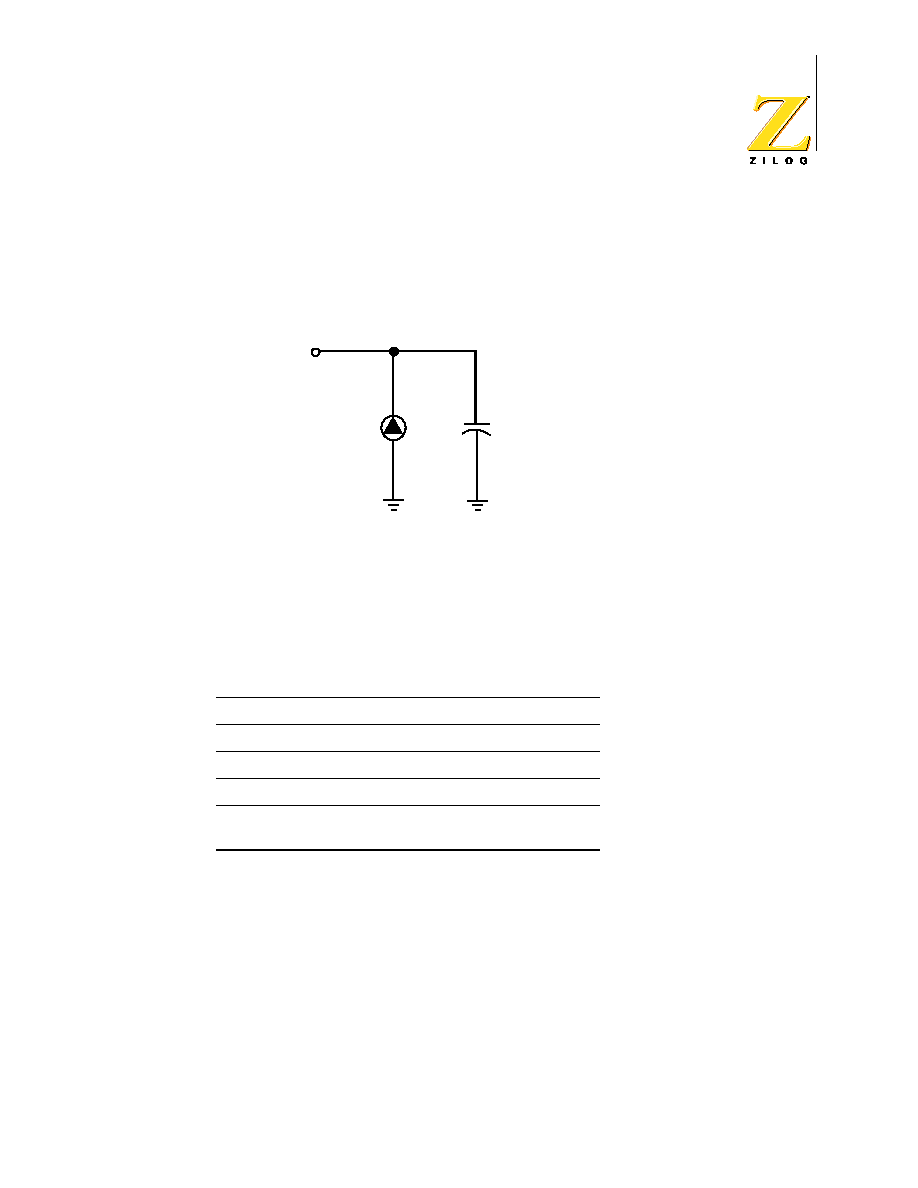
Standard Test Conditions
The characteristics listed below apply for standard test conditions as noted. All
voltages are referenced to GND. Positive current flows into the referenced pin
(see Figure 4).
Figure 4. Test Load Diagram
Capacitance
Table 4 lists the capacitance for the Z86D86 microcontroller.
.
Table 4. Capacitance
Parameter
Max
Input capacitance
12 pF
Output capacitance
12 pF
I/O capacitance
12 pF
Note: T
A
= 25 ∞C, V
CC
= GND = 0 V, f = 1.0 MHz, unmeasured
pins returned to GND.
From Output
Under Test
I

Z86D86
28-Pin Low-Voltage OTP Microcontroller
PS008904-1003
P R E L I M I N A R Y
8
DC Characteristics
Table 5 lists the direct current (DC) characteristics.
Table 5. DC Characteristics
T
A
= 0 ∞C to +70 ∞C
Symbol Parameter
V
CC
Min
Max
Units Conditions
Notes
V
CH
Clock Input High Voltage
2.3 V 0.8 V
CC
V
CC
+ 0.3 V
Driven by External
Clock Generator
5.5 V 0.8 V
CC
V
CC
+ 0.3 V
Driven by External
Clock Generator
V
CL
Clock Input Low Voltage
2.3 V V
SS
≠0.3 0.2 V
CC
V
Driven by External
Clock Generator
5.5 V V
SS
≠0.3 0.2 V
CC
V
Driven by External
Clock Generator
V
IH
Input High Voltage
2.3 V 0.7 V
CC
V
CC
+ 0.3 V
5.5 V 0.7 V
CC
V
CC
+ 0.3 V
V
IL
Input Low Voltage
2.3 V V
SS
≠0.3 0.2 V
CC
V
5.5 V V
SS
≠0.3 0.2 V
CC
V
V
OH1
Output High Voltage
2.3 V V
CC
≠0.4
V
I
OH
= ≠0.5 mA
5.5 V V
CC
≠0.4
V
I
OH
= ≠0.5 mA
V
OH2
Output High Voltage
2.3 V V
CC
≠0.8
V
I
OH
= ≠7 mA
(P36, P37, P00, and P01)
5.5 V V
CC
≠0.8
V
I
OH
= ≠7 mA
V
OL1
Output Low Voltage
2.3 V
0.4
V
I
OL
= 1.0 mA
5.5 V
0.4
V
I
OL
= 4.0 mA
V
OL2
Output Low Voltage
2.3 V
0.8
V
I
OL
= 5.0 mA
1
5.5 V
0.8
V
I
OL
= 7.0 mA
1
V
OL2
Output Low Voltage
2.3 V
0.8
V
I
OL
= 10 mA
(P00, P01, P36, and P37)
5.5 V
0.8
V
I
OL
= 10 mA
V
OFFSET
Comparator Input Offset Voltage 2.3 V
25
mV
5.5 V
25
mV
V
REF
Comparator Reference Voltage
2.3 V 0
V
CC
≠
1.75
V
5.5 V 0
V
CC
≠
1.75
V
I
IL
Input Leakage
2.3 V ≠1
1
µA
V
IN
= 0
V
, V
CC
5.5 V ≠1
1
µA
V
IN
= 0
V
, V
CC
I
OL
Output Leakage
2.3 V ≠1
1
µA
V
IN
= 0
V
, V
CC
5.5 V ≠1
1
µA
V
IN
= 0
V
, V
CC

Z86D86
28-Pin Low-Voltage OTP Microcontroller
PS008904-1003
P R E L I M I N A R Y
9
I
CC
Supply Current
2.3 V
10
mA
@ 8.0 MHz
2, 3
5.5 V
15
mA
@ 8.0 MHz
2, 3
2.3 V
250
µA
@ 32 kHz
2, 3, 4
5.5 V
850
µA
@ 32 kHz
2, 3, 4
I
CC1
Standby Current (HALT Mode)
2.3 V
3
mA
V
IN
= 0
V
, V
CC
@
8.0 MHz
2, 3
5.5 V
5
mA
Same as above
2, 3
2.3 V
2
mA
Clock Divide-by-16
@ 8.0 MHz
2, 3
5.5 V
4
mA
Same as above
2, 3
I
CC2
Standby Current (STOP Mode)
2.3 V
8
µA
V
IN
= 0
V
, V
CC
WDT is not running
5, 6, 9
5.5 V
10
µA
Same as above
5, 6, 9
2.3 V
500
µA
V
IN
= 0
V
, V
CC
WDT is running
5, 6, 9
5.5 V
800
µA
Same as above
5, 6, 9
I
LV
Standby Current (Low Voltage)
100
µA
Vcc < V
LV
7
T
POR
Power-On Reset
2.3 V 12
75
ms
5.5 V 5
20
ms
V
LV
Low Voltage Protection
2
2.3
V
8 MHz max
Ext. CLK Freq.
8
V
LB
Low Battery Detection Flag
2.4
2.7
V
V
LB
= V
LV
+ 0.4 V
Notes:
1. All outputs excluding P00, P01, P36, and P37
2. All outputs unloaded, inputs at rail
3. CL1 = CL2 = 100 pF
4. 32 kHz clock driver input
5. V
LV
increases as the temperature decreases; inputs at V
CC
6. Oscillator stopped
7. Oscillator stops when V
CC
falls below V
LV
limit.
8. V
LV
increases as the temperature decreases.
9. WDT, Comparators, Low Voltage Detection, and ADC (if applicable) are disabled. The IC might draw more
current if any of the above peripherals is enabled.
Table 5. DC Characteristics (Continued)
T
A
= 0 ∞C to +70 ∞C
Symbol Parameter
V
CC
Min
Max
Units Conditions
Notes
Z86D86
28-Pin Low-Voltage OTP Microcontroller
PS008904-1003
P R E L I M I N A R Y
10
AC Characteristics
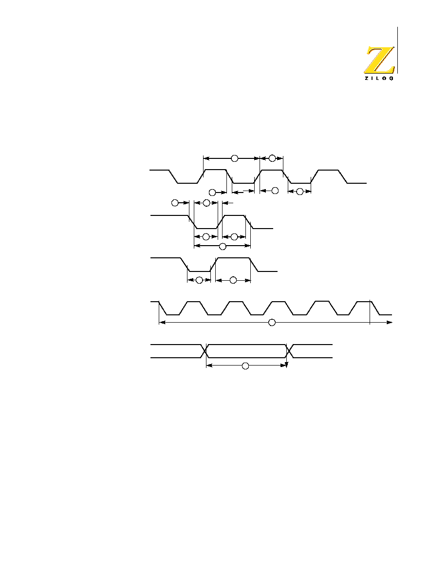
Figure 5 shows the timing diagram. Table 6 describes the alternating current (AC)
characteristics.
Figure 5. Timing Diagram
Clock
T
IN
IRQ
N
Clock
Setup
Stop
Mode
Recovery
Source
2
2
3
3
1
7
7
4
5
6
9
8
11
10

Z86D86
28-Pin Low-Voltage OTP Microcontroller
PS008904-1003
P R E L I M I N A R Y
11
Table 6. AC Characteristics
T
A
= 0∞C to +70∞C
8.0 MHz
Stop-Mode
Recovery
(D1, D0)
Number Symbol
Parameter
V
CC
Min
Max
Units Notes
1
TpC
Input Clock Period
2.3 V
121
DC
ns
1
5.5 V
121
DC
ns
1
2
TrC,TfC
Clock Input Rise and
Fall Times
2.3 V
25
ns
1
5.5 V
25
ns
1
3
TwC
Input Clock Width
2.3 V
37
ns
1
5.5 V
37
ns
1
4
TwTinL
Timer Input
Low Width
2.3 V
100
ns
1
5.5 V
70
ns
1
5
TwTinH
Timer Input High
Width
2.3 V
3TpC
1
5.5 V
3TpC
1
6
TpTin
Timer Input Period
2.3 V
8TpC
1
5.5 V
8TpC
1
7
TrTin,TfTin Timer Input Rise and
Fall Times
2.3 V
100
ns
1
5.5 V
100
ns
1
8A
TwIL
Interrupt Request
Low Time
2.3 V
100
ns
1, 2
5.5 V
70
ns
1, 2
9
TwIH
Interrupt Request
Input High Time
2.3 V
5TpC
1, 2
5.5 V
5TpC
1, 2
10
Twsm
Stop-Mode Recovery
Width Spec
2.3 V
12
ns
5.5 V
12
ns
12
Twdt
Watch-Dog Timer
Delay Time
2.3 V
12
ms
5
0, 0
5.5 V
5
ms
5
2.3 V
24
ms
5
0, 1
5.5 V
10
ms
5
2.3 V
48
ms
5
1, 0
5.5 V
20
ms
5
2.3 V
192
ms
5
1, 1
5.5 V
80
ms
5
Notes:
1. Timing Reference uses 0.9 V
CC
for a logic 1 and 0.1 V
CC
for a logic 0.
2. Interrupt request through Port 3 (P33≠P31)
3. N/A
4. SMR ≠ D5 = 0.
5. For internal RC oscillator

Z86D86
28-Pin Low-Voltage OTP Microcontroller
PS008904-1003
P R E L I M I N A R Y
12
Pin Functions (Standard Mode)
XTAL1 Crystal 1 (Time-Based Input)
This pin connects a parallel-resonant crystal, ceramic resonator, LC, or RC net-
work to the on-chip oscillator input. An external single-phase clock to the on-chip
oscillator input is also an option.
XTAL2 Crystal 2 (Time-Based Output)
This pin connects a parallel-resonant crystal, ceramic resonant, LC, or RC net-
work to the on-chip oscillator output.
Port 0 (P07≠P00)
Port 0 is an 8-bit, bidirectional, CMOS-compatible port. These eight I/O lines are
configured under software control as a nibble I/O port. The output drivers are
push-pull or open drain controlled by bit D2 in the PCON register.
If one or both nibbles are required for I/O operation, they must be configured by
writing to the Port 0 mode register. After a hardware reset, Port 0 is configured as
an input port.
An EPROM option is available to program 0.4 V
CC
CMOS trip inputs on P00≠P03.
This allows direct interface to mouse/trackball IR sensors.
An optional 200
±
50%K
s pull-up transistor is available as a mask option on all
Port 0 bits with nibble select. See Figure 6.
Internal pull-ups are disabled on any given pin or group of port
pins when programmed into output mode.
Note:
Z86D86
28-Pin Low-Voltage OTP Microcontroller
PS008904-1003
P R E L I M I N A R Y
13
Figure 6. Port 0 Configuration
Port 2 (P27≠P20)
Port 2 is an 8-bit, bidirectional, CMOS-compatible I/O port. These eight I/O lines
can be independently configured under software control as inputs or outputs. Port
2 is always available for I/O operation. A mask option is available to connect eight
200 K
(±50%) pull-up transistors on this port. Bits programmed as outputs are
Port 0 (I/O)
Z86D86
MCU
Open-Drain
I/O
EPROM
Option
V
CC
200 KOhms +50%
Pad
Out
In
In
0.4 V
CC
Trip Point Buffer
*EPROM Selectable
4
4
resistive transistor
pull-ups
Z86D86
28-Pin Low-Voltage OTP Microcontroller
PS008904-1003
P R E L I M I N A R Y
14
globally programmed as either push-pull or open-drain. The POR resets with the
eight bits of Port 2 configured as inputs.
Port 2 also has an 8-bit input OR and an AND gate, which can be used to wake up
the part. P20 can be programmed to access the edge-detection circuitry in
demodulation mode. See Figure 7.
Figure 7. Port 2 Configuration
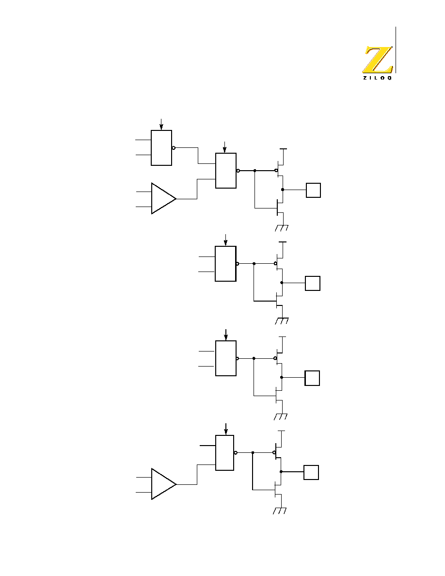
Port 3 (P37≠P31)
Port 3 is a 7-bit, CMOS-compatible fixed I/O port (see Figure 8). Port 3 consists of
three fixed input (P33≠P31) and four fixed output (P37≠P34) ports, and each can
be configured under software control for interrupt, and output from the counter/
Port 2 I/O
Z86D86
MCU
Open-Drain
I/O
EPROM
Option
V
CC
Pad
Out
In
200 KOhms +50%
resistive transistor
pull-ups
Z86D86
28-Pin Low-Voltage OTP Microcontroller
PS008904-1003
P R E L I M I N A R Y
15
timers. P31, P32, and P33 are standard CMOS inputs; P34, P35, P36, and P37
are push-pull outputs.
Figure 8. Port 3 Configuration
Two on-board comparators process analog signals on P31 and P32 with refer-
ence to the voltage on Pref1 and P33. The analog function is enabled by program-
ming the Port 3 Mode Register (bit 1). P31 and P32 are programmable as rising,
falling, or both edge-triggered interrupts (IRQ register bits 6 and 7). Pref1 and P33
are the comparator reference voltage inputs. Access to the counter/timer
edge-detection circuit is through P31 or P20 (see "CTR1 Counter/Timer T8 and
Port 3 (I/O)
Z86D86
MCU
R247 = P3M
P31
P32
P33
P34
P35
P36
P37
+
≠
+
≠
1 = Analog
0 = Digital
P31 (AN1)
Comp1
DIG.
AN.
Pref
D1
P32 (AN2)
Comp1
P33 (Ref2)
From Stop Mode
Recovery Source of SMR
IRQ2, P31 Data Latch
IRQ0, P32 Data Latch
IRQ1, P33 Data Latch
Pref1

Z86D86
28-Pin Low-Voltage OTP Microcontroller
PS008904-1003
P R E L I M I N A R Y
16
T16 Common Control Register" on page 39). Other edge-detect and IRQ modes
are described in Table 7.
Port 3 also provides output for the counter/timers and the AND/OR logic. Control
is performed by programming bits D5≠D4 of CTR1 and bit 0 of CTR2.
Comparator Inputs
In analog mode, P31 and P32 have a comparator front end. The comparator refer-
ence is supplied to P33 and Pref1. In this mode, the P33 internal data latch and its
corresponding IRQ1 are diverted to the SMR sources (excluding P31, P32, and
P33) as indicated in Figure 8 on page 15. In digital mode, P33 is used as D3 of
the Port 3 input register, which then generates IRQ1.
Comparators are powered down by entering STOP Mode. For
P31≠P33 to be used in a Stop-Mode Recovery source, these
inputs must be placed into digital mode.
Comparator Outputs
These outputs can be programmed to output on P34 and P37 through the PCON
register (Figure 9).
Table 7. Pin Assignments
Pin
I/O
C/T
Comp.
Int.
Pref1
RF1
P31
IN
IN
AN1
IRQ2
P32
IN
AN2
IRQ0
P33
IN
RF2
IRQ1
P34
OUT
T8
AO1
P35
OUT
T16
P36
OUT
T8/16
P37
OUT
AO2
P20
I/O
IN
Note:
Z86D86
28-Pin Low-Voltage OTP Microcontroller
PS008904-1003
P R E L I M I N A R Y
17
Figure 9. Port 3 Counter/Timer Output Configuration
+
≠
V
DD
Pad
P34
MUX
PCON, D0
MUX
P34 data
T8_Out
P31
Pref
1
Comp
1
CTR0, D0
V
DD
Pad
P35
MUX
Out 35
T16_Out
CTR2, D0
V
DD
Pad
P36
MUX
Out 36
T8/16_Out
CTR1, D6
V
DD
Pad
P37
MUX
P37 data
PCON, D0
+
≠
P32
Pref
2
Comp
2

Z86D86
28-Pin Low-Voltage OTP Microcontroller
PS008904-1003
P R E L I M I N A R Y
18
Functional Description
The Z86D86 incorporates special functions to enhance the Z8's functionality in
consumer and battery-operated applications.
Program Memory
The Z86D86 family addresses 32 KB of internal program memory. The first twelve
bytes are reserved for interrupt vectors. These locations contain the five 16-bit
vectors that correspond to the five available interrupts.
RAM
The Z86D86 device has 237 bytes of RAM that make up the register file.
Figure 10. Program Memory Map (32K ROM)
Expanded Register File
The register file has been expanded to allow for additional system control regis-
ters and for mapping of additional peripheral devices into the register address
area. The Z8 register address space R0 through R15 has been implemented as
Location of
First byte of
Instruction
Executed
After RESET
16383
12
11
10
9
8
7
6
5
4
3
2
1
0
Not Accessible
On-Chip ROM
Reset Start Address
IRQ5
IRQ5
IRQ4
IRQ4
IRQ3
IRQ3
IRQ2
IRQ2
IRQ1
IRQ1
IRQ0
IRQ0
Interrupt
Vector
(Lower Byte)
Interrupt
Vector
(Upper Byte)

Z86D86
28-Pin Low-Voltage OTP Microcontroller
PS008904-1003
P R E L I M I N A R Y
19
16 banks, with 16 registers per bank. These register groups are known as the
ERF (Expanded Register File). Bits 7≠4 of register RP select the working register
group. Bits 3≠0 of register RP select the expanded register file bank.
An expanded register bank is also referred to as an expanded
register group (see Figure 11).
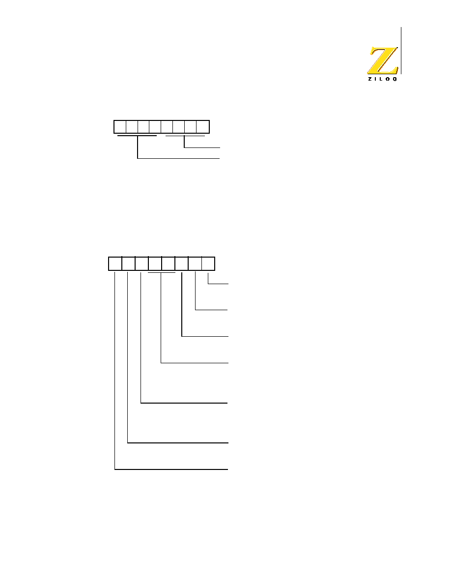
The upper nibble of the register pointer (Figure 12 on page 21) selects which
working register group, of 16 bytes in the register file, is accessed out of the possi-
ble 256. The lower nibble selects the expanded register file bank and, in the case
of the Z86D86 family, banks 0, F, and D are implemented. A 0h in the lower nibble
allows the normal register file (bank 0) to be addressed, but any other value from
1h to Fh exchanges the lower 16 registers to an expanded register bank. For
example, for the Z86D86 (see Figure 11):
R253 RP = 00h
R0 = Port 0
R1 = Port 1
R2 = Port 2
R3 = Port 3
But if:
R253 RP = 0Dh
R0 = CTRL0
R1 = CTRL1
R2 = CTRL2
R3 = Reserved
The counter/timers are mapped into ERF group D. Access is easily performed
using the following:
LD
RP, #0Dh
; Select ERF D for access to bank D
; (working register group 0)
LD
R0,#xx
; load CTRL0
LD
1, #xx
; load CTRL1
LD
R1, 2
; CTRL2
CTRL1
LD
RP, #0Dh
; Select ERF D for access to bank D
; (working register group 0)
LD
RP, #7Dh
; Select expanded register bank D
; working register group 7 of bank 0
; for access.
LD
71h, 2
; CTRL2
register 71h
LD
R1, 2
; CTRL2
register 71h
Note:

Z86D86
28-Pin Low-Voltage OTP Microcontroller
PS008904-1003
P R E L I M I N A R Y
20
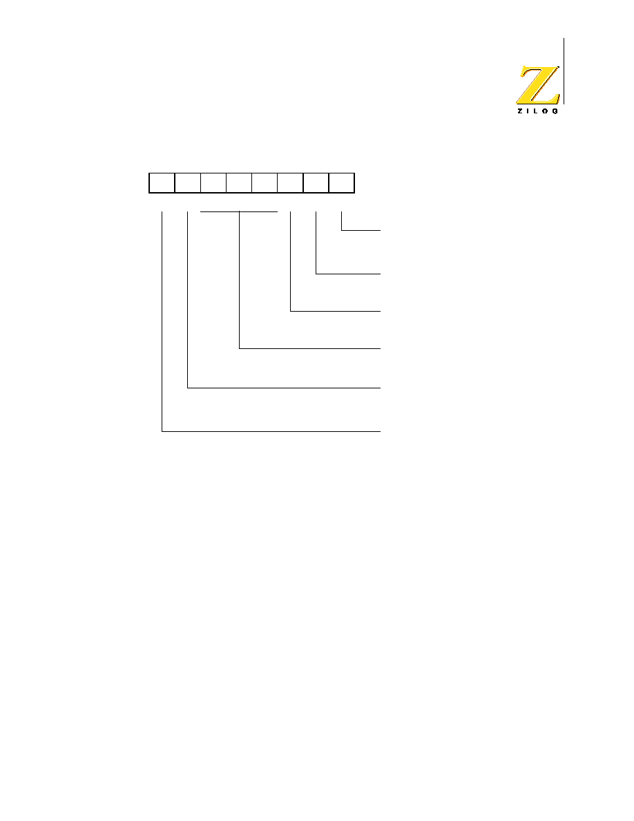
Figure 11.
Expanded Register File Architecture
U U U U U U U U
REGISTER POINTER
7 6 5 4 3 2 1 0
RESET CONDITION
7 6 5 4 3 2 1 0
REGISTER**
EXPANDED REG. BANK (D)
REGISTER**
RESET CONDITION
RESET CONDITION
EXPANDED REG. BANK (F)
REGISTER**
Working Register
Group Pointer
Z8 Register File (Bank 0)**
Expanded Register
Bank Group Pointer
Reserved
Reserved
EXPANDED REG. GROUP (0)
REGISTER**
RESET CONDITION
U = Unknown
* Not reset with a Stop-Mode Recovery
** All addresses are in hexadecimal
Not reset with a Stop-Mode Recovery, except Bit 0.
FF
F0
7F
0F
00
*
*
*
*
FF
FE
FD
FC
FB
FA
F9
F8
F7
F6
F5
F4
F3
F2
F1
F0
(F) 0F
(F) 0E
(F) 0D
(F) 0C
(F) 0B
(F) 0A
(F) 09
(F) 08
(F) 07
(F) 06
(F) 05
(F) 04
(F) 03
(F) 02
(F) 01
(F) 00
(D) 0C
(D) 0B
(D) 0A
(D) 09
(D) 08
(D) 07
(D) 06
(D) 05
(D) 04
(D) 03
(D) 02
(D) 01
(D) 00
LVD
HI8
LO8
HI16
LO16
TC16H
TC16L
TC8H
TC8L
Reserved
CTR2
CTR1
CTR0
U
U
U
U
U
U
U
U
U
0
0
0
U
U
U
U
U
U
U
U
U
U
0
0
U
U
U
U
U
U
U
U
U
U
U
U
U
U
U
U
U
U
U
U
U
U
U
U
U
U
U
U
U
U
U
U
U
U
U
U
U
U
U
U
U
U
U
U
U
U
U
U
U
U
U
U
U
U
U
U
U
U
U
U
U
U
U
U
U
U
U
U
U
0
U
0
WDTMR
Reserved
SMR2
Reserved
SMR
Reserved
Reserved
Reserved
Reserved
Reserved
Reserved
Reserved
Reserved
Reserved
Reserved
PCON
U
U
0
U
U
0
0
U
U
U
1
U
0
0
0
U
0
0
0
U
0
0
0
U
0
0
0
U
0
0
0
U
SPL
SPH
RP
FLAGS
IMR
IRQ
IPR
P01M
P3M
P2M
Reserved
Reserved
Reserved
Reserved
Reserved
Reserved
U
U
0
U
0
0
U
0
0
1
U
U
U
U
0
0
U
U
0
U
0
0
U
1
0
1
U
U
U
U
0
U
U
U
0
U
0
0
U
0
0
1
U
U
U
U
0
U
U
U
0
U
0
0
U
0
0
1
U
U
U
U
0
0
U
U
0
U
0
0
U
1
0
1
U
U
U
U
0
0
U
U
0
U
0
0
U
1
0
1
U
U
U
U
0
0
U
U
0
U
0
0
U
0
0
1
U
U
U
U
0
0
U
U
0
U
0
0
U
1
0
1
U
U
U
U
0
0
*
*
(0) 03
(0) 02
(0) 00
P3
P2
P0
0
U
0
U
U
U
0
U
U
U
U
U
U
U
U
U
Z8 Standard Control Registers
Z86D86
28-Pin Low-Voltage OTP Microcontroller
PS008904-1003
P R E L I M I N A R Y
21
Figure 12. Register Pointer Register
Expanded Register File Control Registers (0D)
Figure 13, Figure 14, Figure 15, and Figure 16 show the expanded register file
control registers (0D).
Figure 13. TC8 Control Register--(0D) OH: Read/Write Except Where Noted
R253 RP
D7 D6 D5
D4 D3 D2 D1 D0
Expanded Register
File Pointer
Working Register
Pointer
Default setting after reset = 0000 0000
D7 D6 D5 D4 D3 D2 D1 D0
0 = P34 as Port Output *
* Default setting after reset
1 = Timer8 Output
0 = Disable T8 Time-out Interrupt
1 = Enable T8 time-out Interrupt
1 = Enable T8 Data Capture Interrupt
0 = Disable T8 Data Capture Interrupt
00 = SCLK on T8
01 = SCLK/2 on T8
10 = SCLK/4 on T8
11 = SCLK/8 on T8
R = 0 No T8 Counter Time-out
R = 1 T8 Counter Time-out Occurred
W = 0 No Effect
W = 1 Reset Flag to 0
1 = Single Pass
0 = Modulo-N
R = 0 T8 Disabled *
R = 1 T8 Enabled
W = 0 Stop T8
W = 1 Enable T8
CTR1 (0D) 0H

Z86D86
28-Pin Low-Voltage OTP Microcontroller
PS008904-1003
P R E L I M I N A R Y
22
Figure 14. T8 and T16 Common Control Functions--(0D) 1H: Read/Write
D7 D6 D5 D4 D3 D2 D1 D0
Transmit Mode
R/W 0 Reserved
1 Reserved
Demodulation Mode
R 0 = No Falling Edge Detection
R 1 = Falling Edge Detection
W 0 = No Effect
W 1 = Reset Flag to 0
Transmit Mode
R/W 0 = T8_OUT is 0 initially
R/W 1 = T8_OUT is 1 initially
Demodulation Mode
R 0 = No Rising Edge Detection
R 1 = Rising Edge Detection
W 0 = No Effect
W 1 = Reset flag to 0
Transmit Mode
0 0 = Normal Operation
0 1 = Ping-Pong Mode
1 0 T16_OUT = 0
1 1 T16_OUT = 1
Demodulation Mode
0 0 = No Filter
0 1 = 4 SCLK Cycle Filter
1 0 = 8 SCLK Cycle Filter
1 1 = Reserved
Transmit Mode/T8/T16 Logic
0 0 = AND
0 1 = OR
1 0 = NOR
1 1 = NAND
Demodulation Mode
0 0 = Falling Edge Detection
0 1 = Rising Edge Detection
1 0 = Both Edge Detection
1 1 = Reserved
Transmit Mode
0 = P36 as Port Output *
1 = P36 as T8/T16_OUT
Demodulation Mode
0 = P31 as Demodulator Input
1 = P20 as Demodulator Input
Transmit/Demodulation Modes
0 = Transmit Mode *
1 = Demodulation Mode
* Default setting after reset
CTR1 (0D) 1H
Note: Care must be taken in differentiating
Note: Changing from one mode to
transmit mode from demodulation mode.
Depending on which of these two modes is
operating, the CTR1 bit has different
functions.
another cannot be done without
disabling the counter/timers.

Z86D86
28-Pin Low-Voltage OTP Microcontroller
PS008904-1003
P R E L I M I N A R Y
23
Figure 15. T16 Control Register--(0D) 2H: Read/Write Except Where Noted
D7 D6 D5 D4 D3 D2 D1 D0
0 = P35 is Port Output *
* Default setting after reset
1 = P35 is TC16 Output
0 = Disable T16 Time-out Interrupt
1 = Enable T16 time-out Interrupt
1 = Enable T16 Data Capture Interrupt
0 = Disable T16 Data Capture Interrupt
00 = SCLK on T16
01 = SCLK/2 on T16
10 = SCLK/4 on T16
11 = SCLK/8 on T16
R = 0 No T16 Time-out
R = 1 T16 Time-out Occurs
W = 0 No Effect
W = 1 Reset Flag to 0
R = 0 T16 Disabled *
R = 1 T16 Enabled
W = 0 Stop T16
W = 1 Enable T16
CTR2 (0D) 02H
Transmit Mode
0 = Modulo-N for T16
1 = Single Pass for T16
Demodulator Mode
0 = T16 Recognizes Edge
1 = T16 doe Not Recognize Edge
Z86D86
28-Pin Low-Voltage OTP Microcontroller
PS008904-1003
P R E L I M I N A R Y
24
Figure 16. Low Battery Detection
D7 D6 D5 D4 D3 D2 D1 D0
LBD (0D) 0CH
0: disable*
LBD Flag (read only)
*Default
0: LBD flag reset*
1: LBD flag set
Reserved (must be 0)
1: enable
Low Battery Detection at VLV + 0.4 V

Z86D86
28-Pin Low-Voltage OTP Microcontroller
PS008904-1003
P R E L I M I N A R Y
25
Expanded Register File Control Registers (0F)
Figure 17 through Figure 30 show the expanded register file control registers (0F).
Figure 17. Stop-Mode Recovery Register--(0F) 0BH: D6≠D0 = Write Only, D7 = Read
Only
D7 D6 D5 D4 D3 D2 D1 D0
SCLK/TCLK Divide-by-16
0 = OFF **
Reserved (must be 0)
Stop-Mode Recovery Source
SMR (0F) 0B
1 = ON
000 = POR Only *
001 = Reserved
010 = P31
011 = P32
100 = P33
101 = P27
110 = P2 NOR 0≠3
111 = P2 NOR 0≠7
Stop Delay
Reserved (must be 1)
1 = ON*
Stop Recovery Level ***
0 = Low *
1 = High
Stop Flag
0 = POR *
1 = Stop Recovery **
* Default setting after reset
** Default setting after reset and Stop-Mode Recovery
*** At the XOR gate input

Z86D86
28-Pin Low-Voltage OTP Microcontroller
PS008904-1003
P R E L I M I N A R Y
26
Figure 18. Stop-Mode Recovery Register 2--(0F) 0DH: D2≠D4, D6 Write Only
D7 D6 D5 D4 D3 D2 D1 D0
Reserved (must be 0)
Stop-Mode Recovery Source
SMR2 (0F) DH
000 = POR Only *
001 = NAND P20, P21, P22, P23
010 = NAND P20, P21, P22, P23, P24, P25, P26, P27
011 = NOR P31, P32, P33
100 = NAND P31, P32, P33
101 = NOR P31, P32, P33, P00, P07
110 = NAND P31, P32, P33, P00, P07
111 = NAND P31, P32, P33, P20, P21, P22
Reserved (must be 0)
Recovery Level **
0 = Low *
1 = High
* Default setting after reset
** At the XOR gate input
Reserved (must be 0)
Reserved (must be 0)
Note: If used in conjunction with SMR,
either of the two specified events
causes a Stop-Mode Recovery.
Z86D86
28-Pin Low-Voltage OTP Microcontroller
PS008904-1003
P R E L I M I N A R Y
27
Figure 19. Watch-Dog Timer Register--(0F) 0FH: Write Only
Figure 20. Port Configuration Register (PCON)--(0F) 0H: Write Only
D7 D6 D5 D4 D3 D2 D1 D0
WDT TAP INT RC OSC External Clock
* Default setting after reset
00 5 ms min 256 TpC
01* 10 ms min 512 TpC
10 20 ms min 1024 TpC
11 80 ms min 4096 TpC
WDT during HALT
0 = OFF
1 = ON*
WDT during STOP
0 = OFF
1 = ON*
Reserved (must be 0)
WDTMR (0F) 0F
XTAL/INT RC Select for WDT
0 = RC OSC
1 = XTAL
D7 D6 D5 D4 D3 D2 D1 D0
Comparator Output Port 3
Reserved (must be 1)
Port 0
0 = Open-drain
1 = Push-pull*
Reserved (must be 1)
*Default setting after reset
PCON (FH) 00H
0 P34, P37, Standard Output*
1 P34, P37, Comparator Output
Z86D86
28-Pin Low-Voltage OTP Microcontroller
PS008904-1003
P R E L I M I N A R Y
28
Figure 21. Port 2 Mode Register--F6H: Write Only
Figure 22. Port 3 Mode Register--F7H: Write Only
D7 D6 D5 D4 D3 D2 D1 D0
R246 P2M
P27≠P20 I/O Definition
0 = Defines bit as OUTPUT
1 = Defines bit as IINPUT *
*Default setting after reset
D7 D6 D5 D4 D3 D2 D1 D0
R247 P3M
0 = Port 2 Open-drain *
1 = Port 2 Push-Pull
*Default setting after reset
0 = P31, P32 Digital Mode
1 = P31, P32 analog Mode
Reserved (must be 0)
Z86D86
28-Pin Low-Voltage OTP Microcontroller
PS008904-1003
P R E L I M I N A R Y
29
R248 P01M
Figure 23. Port 0 and 1 Mode Register--F8H: Write Only
D7
D6
D5
D4
D3
D2
D1
D0
P00≠P03 Mode
0: Output
1: Input *
Reserved; must be 0
Reserved; must be 1
Reserved; must be 0
P07≠P04 Mode
0: Output
1: Input *
Reserved; must be 0
* Default setting after reset
Z86D86
28-Pin Low-Voltage OTP Microcontroller
PS008904-1003
P R E L I M I N A R Y
30
Figure 24. Interrupt Priority Register--F9H: Write Only
Figure 25. Interrupt Request Register--FAH: Read/Write
D7 D6 D5 D4 D3 D2 D1 D0
R249 IPR
Interrupt Group Priority
000 = Reserved
Reserved (must be 0)
001 = C>A>B
101 = A>B>C
011 = A>C>B
100 = B>C>A
101 = C>B>A
110 = B>A>C
111 = Reserved
IRQ1, IRQ, Priority (Group C)
0 = IRQ1>IRQ4
1 = IRQ4>IRQ1
IRQ0, IRQ2, Priority (Group B)
0 = IRQ2>IRQ0
1 = IRQ0>IRQ2
IRQ3, IRQ5, Priority (Group A)
0 = IRQ5>IRQ3
1 = IRQ3>IRQ5
D7 D6 D5 D4 D3 D2 D1 D0
R250 IRQ
IRQ0 = P32 Input
IRQ1 = P23 Input
IRQ2 = P31 Input
IRQ3 = T16
IRQ4 = T8
Inner Edge
P31
P32
= 00
P31
P32
= 01
P31
P32
= 10
P31
P32
= 11
IRQ5 = LBD

Z86D86
28-Pin Low-Voltage OTP Microcontroller
PS008904-1003
P R E L I M I N A R Y
31
Figure 26. Interrupt Mask Register--FBH: Read/Write
Figure 27. Flag Register--FCH: Read/Write
D7 D6 D5 D4 D3 D2 D1 D0
R251 IMR
1 = Enables IRQ5≠IRQ0
(D0 = IRQ0)
Reserved (must be 0)
0 = Master Interrupt Disable *
1 = Master Interrupt Enable **
* Default setting after reset
** Only by using E1, D1 instruction. D1 is required before changing the IMR register.
D7 D6 D5 D4 D3 D2 D1 D0
R252 Flags
User Flag F1
User Flag F2
Half Carry Flag
Decimal Adjust Flag
Overflow Flag
Sign Flag
Zero Flag
Carry Flag
Z86D86
28-Pin Low-Voltage OTP Microcontroller
PS008904-1003
P R E L I M I N A R Y
32
Figure 28. Register Pointer--FDH: Read/Write
Figure 29. Stack Pointer High--FEH: Read/Write
Figure 30. Stack Pointer Low--FFH: Read/Write
Register File
The register file (bank 0) consists of four I/O port registers, 237 general-purpose
registers, and 16 control and status registers (R0≠R3, R4≠R239, and R240≠255,
respectively). Additional, there are two expanded registers groups in Banks D and
F. Instructions can access registers directly or indirectly through an 8-bit address
field, thereby allowing a short, 4-bit register address to use the Register Pointer
(Figure 31). In the 4-bit mode, the register file is divided into 16 working register
groups, each occupying 16 continuous locations. The Register Pointer addresses
the starting location of the active working register group.
Working register group E0≠EF can only be accessed through
working registers and indirect addressing modes.
D7 D6 D5 D4 D3 D2 D1 D0
Expanded Register Bank
Pointer
Working Register
Pointer
R253 RP
Default setting after
reset = 0000 0000
D7 D6 D5 D4 D3 D2 D1 D0
General Purpose Register
Byte (SP15≠SP8)
R254 SPH
D7 D6 D5 D4 D3 D2 D1 D0
Stack Pointer Lower
Byte (SP7≠SP0)
R255 SPL
Note:

Z86D86
28-Pin Low-Voltage OTP Microcontroller
PS008904-1003
P R E L I M I N A R Y
33
Figure 31. Register Pointer
Stack
The Z86D86 internal register file is used for the stack. An 8-bit Stack Pointer
(R255) is used for the internal stack that resides in the general-purpose registers
(R4≠R239). SPH is used as a general-purpose register only when using internal
stacks.
When SPH is used as a general-purpose register and Port 0 is
in address mode, the contents of SPH are loaded into Port 0
whenever the internal stack is accessed.
7F
70
6F
60
5F
50
4F
40
3F
30
2F
20
1F
10
0F
00
00
r
7
r
6
r
5
r
4
r
3
r
2
r
1
r
0
The upper nibble of the register file address
provided by the register pointer specifies
the active working-register group
R253
Specified Working
Register Group
The lower nibble
of the register
file address
provided by the
Instruction points
to the specified
register
Register Group 1
Register Group 2
I/O Ports
R15 to R0
R15 to R4*
R3 to R0*
* RP =00: Selects Register Group 0, Working Register 0
Note:

Z86D86
28-Pin Low-Voltage OTP Microcontroller
PS008904-1003
P R E L I M I N A R Y
34
Counter/Timer Registers
Table 8 describes the expanded register group D.
Register Description
LBD(D)0Ch--Low Battery Detection Register
Bit 0 enables/disables the Low Battery Detection Circuit. Bit 1 flags if low battery is
detected. Interrupt 5 is triggered when the flag bit is set, given that IRQ5 is not
masked. See Table 9.
The LVD flag will be valid after enabling the detection for 20
µ
S
(design estimation, not tested in production). LVD does not
work at STOP mode. It must be disabled during STOP mode in
order to reduce current.
Table 8. Expanded Register Group D
(D)0Ch
LVD
(D)0Bh
HI8
(D)0Ah
LO8
(D)09h
HI16
(D)08h
LO16
(D)07h
TC16H
(D)06h
TC16L
(D)05h
TC8H
(D)04h
TC8L
(D)03h
Reserved
(D)02h
CTR2
(D)01h
CTR1
(D)00h
CTR0
Note:

Z86D86
28-Pin Low-Voltage OTP Microcontroller
PS008904-1003
P R E L I M I N A R Y
35
HI8(D)0Bh
This register (Table 10) holds the captured data from the output of the 8-bit
Counter/Timer0. This register is typically used to hold the number of counts when
the input signal is 1.
L08(D)0Ah
This register (Table 11) holds the captured data from the output of the 8-bit
Counter/Timer0. This register is typically used to hold the number of counts when
the input signal is 0.
.
HI16(D)09h
This register (Table 12) holds the captured data from the output of the 16-bit
Counter/Timer16. This register holds the MS-Byte of the data.
Table 9. LBD(D)0C--Low Battery Detection Register
Field
Bit Position
Description
LBD
765432--
Reserved
No effect
------1-
R
1
0*
LB flag set
LB flag reset
-------0
R/W 1
0*
Enable LBD
Disable LBD
Note:
*Default after POR
Table 10. HI8(D)0Bh
Field
Bit Position
Description
T8_Capture_HI
76543210
R
W
Captured Data
No Effect
Table 11.
L08(D)0Ah
Field
Bit Position
Description
T8_Capture_L0
76543210
R
W
Captured Data
No Effect

Z86D86
28-Pin Low-Voltage OTP Microcontroller
PS008904-1003
P R E L I M I N A R Y
36
L016(D)08h
This register (Table 13) holds the captured data from the output of the 16-bit
Counter/Timer16. This register holds the LS-Byte of the data.
TC16H(D)07h
Table 14 describes the Counter/Timer2 MS-Byte Hold Register.
TC16L(D)06h
Table 15 describes the Counter/Timer2 LS-Byte Hold Register.
TC8H(D)05h
Table 16 describes the Counter/Timer8 High Hold Register.
Table 12.
HI16(D)09h
Field
Bit Position
Description
T16_Capture_HI
76543210
R
W
Captured Data
No Effect
Table 13. L016(D)08h
Field
Bit Position
Description
T16_Capture_LO
76543210
R
W
Captured Data
No Effect
Table 14. TC16H(D)07h
Field
Bit Position
Description
T16_Data_HI
76543210
R/W
Data
Table 15. TC16L(D)06h
Field
Bit Position
Description
T16_Data_LO
76543210
R/W
Data

Z86D86
28-Pin Low-Voltage OTP Microcontroller
PS008904-1003
P R E L I M I N A R Y
37
TC8L(D)04h
Table 17 describes the Counter/Timer8 Low Hold Register.
CTR0 Counter/Timer8 Control Register
Table 18 describes the CTR0 (D)00 Counter/Timer8 Control Register.
Table 16. TC8H(D)05h
Field
Bit Position
Description
T8_Level_HI
76543210
R/W Data
Table 17. TC8L(D)04h
Field
Bit Position
Description
T8_Level_LO
76543210
R/W
Data
Table 18. CTR0 (D)00 Counter/Timer8 Control Register
Field
Bit Position
Value
Description
T8_Enable
7-------
R
W
0*
1
0
1
Counter Disabled
Counter Enabled
Stop Counter
Enable Counter
Single/Modulo-N
-6-------
R/W
0
1
Modulo-N
Single Pass
Time_Out
--5------
R
W
0
1
0
1
No Counter Time-Out
Counter Time-Out Occurred
No Effect
Reset Flag to 0
T8 _Clock
---43---
R/W 0
0
0 1
1 0
1 1
SCLK
SCLK/2
SCLK/4
SCLK/8
Capture_INT_MASK
-----2--
R/W
0
1
Disable Data Capture Int.
Enable Data Capture Int.
Z86D86
28-Pin Low-Voltage OTP Microcontroller
PS008904-1003
P R E L I M I N A R Y
38
T8 Enable
This field enables T8 when set (written) to 1.
Single/Modulo-N
When set to 0 (modulo-n), the counter reloads the initial value when the terminal
count is reached. When set to 1 (single pass), the counter stops when the terminal
count is reached.
Time-Out
This bit is set when T8 times out (terminal count reached). To reset this bit, a 1
must be written to this location.
Writing a 1 is the only way to reset the Terminal Count
status condition. Therefore, you must reset this bit before
using/enabling the counter/timers.
The first clock of T8 might not exhibit complete clock width
and can occur anytime when enabled.
Care must be taken when utilizing the OR or AND commands
to manipulate CTR0, bit 5 and CTR1, bits 0 and 1
(demodulation mode). These instructions use a Read-Modify-
Write sequence in which the current status from the CTR0 and
CTR1 registers is ORed or ANDed with the designated value
and then written back into the registers.
For example, when the status of bit 5 is 1, a timer reset condition occurs.
T8 Clock
This bit defines the frequency of the input signal to T8.
Counter_INT_Mask
------1-
R/W
0
1
Disable Time-Out Int.
Enable Time-Out Int.
P34_Out
-------0
R/W
0*
1
P34 as Port Output
T8 Output on P34
Note:
* Indicates the value upon Power-On Reset.
Table 18. CTR0 (D)00 Counter/Timer8 Control Register (Continued)
Field
Bit Position
Value
Description
Caution:
Note:

Z86D86
28-Pin Low-Voltage OTP Microcontroller
PS008904-1003
P R E L I M I N A R Y
39
Capture_INT_Mask
Set this bit to allow an interrupt when data is captured into either LO8 or HI8 upon
a positive or negative edge detection in demodulation mode.
Counter_INT_Mask
Set this bit to allow an interrupt when T8 has a time-out.
P34_Out
This bit defines whether P34 is used as a normal output pin or the T8 output.
CTR1 Counter/Timer T8 and T16 Common Control Register
This register controls the functions in common with the T8 and T16. See Table 19.
Table 19. CTR1(D)01h Register
Field
Bit Position
Value
Description
Mode
7-------
R/W 0*
Transmit Mode
Demodulation Mode
P36_Out/Demodulator_Input
-6------
R/W
0*
1
0
1
Transmit Mode
Port Output
T8/T16 Output
Demodulation Mode
P31
P20
T8/T16_Logic/Edge _Detect
--54----
R/W
00
01
10
11
00
01
10
11
Transmit Mode
AND
OR
NOR
NAND
Demodulation Mode
Falling Edge
Rising Edge
Both Edges
Reserved

Z86D86
28-Pin Low-Voltage OTP Microcontroller
PS008904-1003
P R E L I M I N A R Y
40
Mode
If it is 0, the counter/timers are in the transmit mode; otherwise, they are in the
demodulation mode.
P36_Out/Demodulator_Input
In transmit mode, this bit defines whether P36 is used as a normal output pin or
the combined output of T8 and T16.
In demodulation mode, this bit defines whether the input signal to the counter/tim-
ers is from P20 or P31.
Transmit_Submode/Glitch_Filter
----32--
R/W
00
01
10
11
00
01
10
11
Transmit Mode
Normal Operation
Ping-Pong Mode
T16_Out = 0
T16_Out = 1
Demodulation Mode
No Filter
4 SCLK Cycle
8 SCLK Cycle
Reserved
Initial_T8_Out/Rising Edge
------1-
R/W
R
W
0
1
0
1
0
1
Transmit Mode
T8_OUT is 0 Initially
T8_OUT is 1 Initially
Demodulation Mode
No Rising Edge
Rising Edge Detected
No Effect
Reset Flag to 0
Initial_T16_Out/Falling_Edge
-------0
R/W
R
W
0
1
0
1
0
1
Transmit Mode
T16_OUT is 0 initially.
T16_OUT is 1 initially.
Demodulation Mode
No Falling Edge
Falling Edge Detected
No Effect
Reset Flag to 0
Note:
*Default upon Power-On Reset
Table 19. CTR1(D)01h Register (Continued)
Field
Bit Position
Value
Description

Z86D86
28-Pin Low-Voltage OTP Microcontroller
PS008904-1003
P R E L I M I N A R Y
41
T8/T16_Logic/Edge _Detect
In transmit mode, this field defines how the outputs of T8 and T16 are combined
(AND, OR, NOR, NAND).
In demodulation mode, this field defines which edge needs to be detected by the
edge detector.
Transmit_Submode/Glitch Filter
In transmit mode, this field defines whether T8 and T16 are in the "Ping-Pong"
mode or in independent normal operation mode. Setting this field to "Normal
Operation Mode" terminates the "Ping-Pong Mode" operation. When set to 10,
T16 is immediately forced to a 0; a setting of 11 forces T16 to output a 1.
In demodulation mode, this field defines the width of the glitch that needs to be fil-
tered out.
Initial_T8_Out/Rising_Edge
In transmit mode, if 0, the output of T8 is set to 0 when it starts to count. If 1, the
output of T8 is set to 1 when it starts to count. When the counter is not enabled
and this bit is set to 1 or 0, T8_OUT is set to the opposite state of this bit. This
measure ensures that when the clock is enabled, a transition occurs to the initial
state set by CTR1, D1.
In demodulation mode, this bit is set to 1 when a rising edge is detected in the
input signal. In order to reset it, a 1 must be written to this location.
Initial_T16 Out/Falling _Edge
In transmit mode, if it is 0, the output of T16 is set to 0 when it starts to count. If it
is 1, the output of T16 is set to 1 when it starts to count. This bit is effective only in
Normal or Ping-Pong Mode (CTR1, D3, D2). When the counter is not enabled and
this bit is set, T16_OUT is set to the opposite state of this bit. This measure
ensures that when the clock is enabled, a transition occurs to the initial state set
by CTR1, D0.
In demodulation mode, this bit is set to 1 when a falling edge is detected in the
input signal. In order to reset it, a 1 must be written to this location.
Modifying CTR1 (D1 or D0) while the counters are enabled
causes unpredictable output from T8/16_OUT.
Note:

Z86D86
28-Pin Low-Voltage OTP Microcontroller
PS008904-1003
P R E L I M I N A R Y
42
CTR2 Counter/Timer16 Control Register
Table 20 describes the contents of the CTR2 register.
T16_Enable
This field enables T16 when set to 1.
Single/Modulo-N
In transmit mode, when this bit is set to 0, the counter reloads the initial value
when terminal count is reached. When this bit is set to 1, the counter stops when
the terminal count is reached.
Table 20. CTR2 (D)02h: Counter/Timer16 Control Register
Field
Bit Position
Value
Description
T16_Enable
7-------
R
W
0*
1
0
1
Counter Disabled
Counter Enabled
Stop Counter
Enable Counter
Single/Modulo-N
-6------
R/W
0
1
0
1
Transmit Mode
Modulo-N
Single Pass
Demodulation Mode
T16 Recognizes Edge
T16 Does Not Recognize Edge
Time_Out
--5-----
R
W
0
1
0
1
No Counter Time-Out
Counter Time-Out Occurred
No Effect
Reset Flag to 0
T16 _Clock
---43---
R/W
00
01
10
11
SCLK
SCLK/2
SCLK/4
SCLK/8
Capture_INT_Mask
-----2--
R/W
0
1
Disable Data Capture Int.
Enable Data Capture Int.
Counter_INT_Mask
------1-
R/W
0
Disable Time-Out Int.
Enable Time-Out Int.
P35_Out
-------0
R/W
0*
1
P35 as Port Output
T16 Output on P35
Note:
* Indicates the value upon Power-On Reset.

Z86D86
28-Pin Low-Voltage OTP Microcontroller
PS008904-1003
P R E L I M I N A R Y
43
In demodulation mode, when this bit is set to 0, T16 captures and reloads on
detection of all the edges. When this bit is set to 1, T16 captures and detects on
the first edge, but ignores the subsequent edges. For details, see "T16 Demodula-
tion Mode" on page 51.
Time_Out
This bit is set when T16 times out (terminal count reached). In order to reset this
bit, a 1 must be written to this location.
T16_Clock
This bit defines the frequency of the input signal to Counter/Timer16.
Capture_INT_Mask
This bit is set to allow an interrupt when data is captured into LO16 and HI16.
Counter_INT_Mask
This bit is set to allow an interrupt when T16 times out.
P35_Out
This bit defines whether P35 is used as a normal output pin or T16 output.
Counter/Timer Functional Blocks
The following are the counter/timer functional blocks:
∑
Input circuit
∑
Eight-bit counter/timer circuits (page 44)
∑
Sixteen-bit counter/timer circuits (page 50)
∑
Output circuit (page 54)
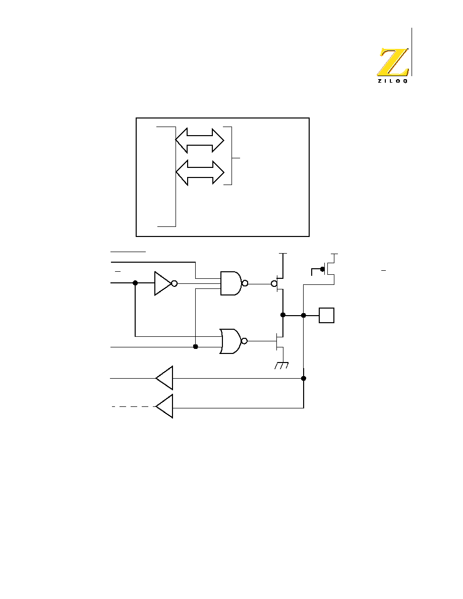
Input Circuit
The edge detector monitors the input signal on P31 or P20. Based on CTR1 D5≠
D4, a pulse is generated at the Pos Edge or Neg Edge line when an edge is
detected. Glitches in the input signal that have a width less than specified (CTR1
D3, D2) are filtered out (see Figure 32).

Z86D86
28-Pin Low-Voltage OTP Microcontroller
PS008904-1003
P R E L I M I N A R Y
44
Figure 32. Glitch Filter Circuitry
Eight-Bit Counter/Timer Circuits
Figure 33 shows the 8-bit counter/timer circuits.
Figure 33. 8-Bit Counter/Timer Circuits
CTR1 D5, D4
P31
P20
MUX
CTR1 D6
Glitch Filter
Edge Detector
Pos Edge
Neg Edge
CTR1 D3, D2
Z8 Data Bus
Pos Edge
Neg Edge
CTR0 D4, D3
SCLK
Z8 Data Bus
Clock
Select
Clock
8-Bit
Counter T8
TC8H
TC8L
CTR0 D2
IRQ4
CTR0 D1
T8_OUT
HI8
LO8

Z86D86
28-Pin Low-Voltage OTP Microcontroller
PS008904-1003
P R E L I M I N A R Y
45
T8 Transmit Mode
Before T8 is enabled, the output of T8 depends on CTR1, D1. If it is 0, T8_OUT is
1. If it is 1, T8_OUT is 0.
When T8 is enabled, the output T8_OUT switches to the initial value (CTR1, D1).
If the initial value (CTR1, D1) is 0, TC8L is loaded; otherwise, TC8H is loaded into
the counter (see Figure 34). In Single-Pass Mode (CTR0, D6), T8 counts down to
0 and stops, T8_OUT toggles, and the time-out status bit (CTR0, D5) is set. A
time-out interrupt can be generated if it is enabled (CTR0, D1). See Figure 35. In
Modulo-N Mode, upon reaching terminal count, T8_OUT is toggled, but no inter-
rupt is generated. Then T8 loads a new count (if the T8_OUT level now is 0),
TC8L is loaded; if it is 1, TC8H is loaded. T8 counts down to 0, toggles T8_OUT,
sets the time-out status bit (CTR0, D5) and generates an interrupt if enabled
(CTR0, D1). One cycle is thus completed. T8 then loads from TC8H or TC8L
according to the T8_OUT level, and repeats the cycle. See Figure 36.

Z86D86
28-Pin Low-Voltage OTP Microcontroller
PS008904-1003
P R E L I M I N A R Y
46
Figure 34. Transmit Mode Flowchart
T8 (8-Bit)
Transmit Mode
No
T8_Enable Bit
Set CTR0, D7
Yes
Reset T8_Enable Bit
Load TC8L
Reset T8_OUT
Load TC8H
Set T8_OUT
Enable T8
No
T8_Timeout
Yes
Single Pass
Single Pass?
Modulo-N
T8_OUT Value
1
0
Load TC8H
Set T8_OUT
Enable T8
No
T8_Timeout
Yes
Set Time-out Status Bit
(CTR0, D5) and generate
Timeout_Int if enabled
Set Time-out Status Bit
(CTR0, D5) and generate
Temeout_Int if enabled
CTR1, D1
Value
Load TC8L
Reset T8_OUT

Z86D86
28-Pin Low-Voltage OTP Microcontroller
PS008904-1003
P R E L I M I N A R Y
47
Figure 35. T8_OUT in Single-Pass Mode
Figure 36. T8_OUT in Modulo-N Mode
You can modify the values in TC8H or TC8L at any time. The new values take
effect when they are loaded. T ensure known operation, do not to write these reg-
isters at the time the values are to be loaded into the counter/timer.
An initial count
of 1 is not allowed (a nonfunction occurs).
An initial count of 0 causes TC8 to count
from 0 to FFh to FEh.
"h" is used for hexadecimal values.
Transition from 0 to FFh is not a time-out condition.
Do not use the same instructions for stopping the counter/
timers and setting the status bits.
Two successive commands are necessary. First, the counter/timers must be
stopped, and second, the status bits must be reset. These commands are
required because it takes one counter/timer clock interval for the initiated event to
actually occur.
T8 Demodulation Mode
You need to program TC8L and TC8H to FFh. After T8 is enabled, when the first
edge (rising, falling, or both, depending on CTR1, D5, D4) is detected, it starts to
count down. When a subsequent edge (rising, falling, or both, depending on
CTR1, D5, D4) is detected during counting, the current value of T8 is one's com-
plemented and put into one of the capture registers. If it is a positive edge, data is
TC8H Counts
Counter Enable Command,
T8_OUT switches to its
initial value (CTR1 D1)
T8_OUT toggles
Time-out Interrupt
T8_OUT
TC8L
TC8H
Time-out
Interrupt
Counter Enable Command,
T8_OUT switches to its
initial value (CTR1 D1)
T8_OUT Toggles
TC8L
TC8H
TC8L
Time-out
Interrupt
Note:
Caution:

Z86D86
28-Pin Low-Voltage OTP Microcontroller
PS008904-1003
P R E L I M I N A R Y
48
put into LO8; if it is a negative edge, HI8. From that point, one of the edge-detect
status bits (CTR1, D1, D0) is set, and an interrupt can be generated if enabled
(CTR0, D2). Meanwhile, T8 is loaded with FFh and starts counting again. If T8
reaches 0, the time-out status bit (CTR0, D5) is set, an interrupt can be generated
if enabled (CTR0, D1), and T8 continues counting from FFh (see Figure 37 and
Figure 38).
Figure 37. Demodulation Mode Count Capture Flowchart
No
Yes
Pos
Neg
T8 LO8
T8 HI8
FFh T8
What Kind
of Edge
Edge
Present
T8_Enable
(Set by User)
T8 (8-Bit)
Count Capture
No
Yes

Z86D86
28-Pin Low-Voltage OTP Microcontroller
PS008904-1003
P R E L I M I N A R Y
49
Figure 38. Demodulation Mode Flowchart
T8 (8-Bit)
Demodulation
T8 Enable
CTR0, D7
No
Yes
FFh TC8
First Edge
Present
No
Yes
Enable TC8
Disable T8
T8_Enable Bit Set
Edge Present
No
Yes
T8 Time-out
No
Yes
Set Edge Present Status
Bit and Trigger Data
Capture Int. if enabled
Continue Counting
Set Edge Present Status
Bit and Trigger Time
Out Int. if enabled
Mode
No
Yes
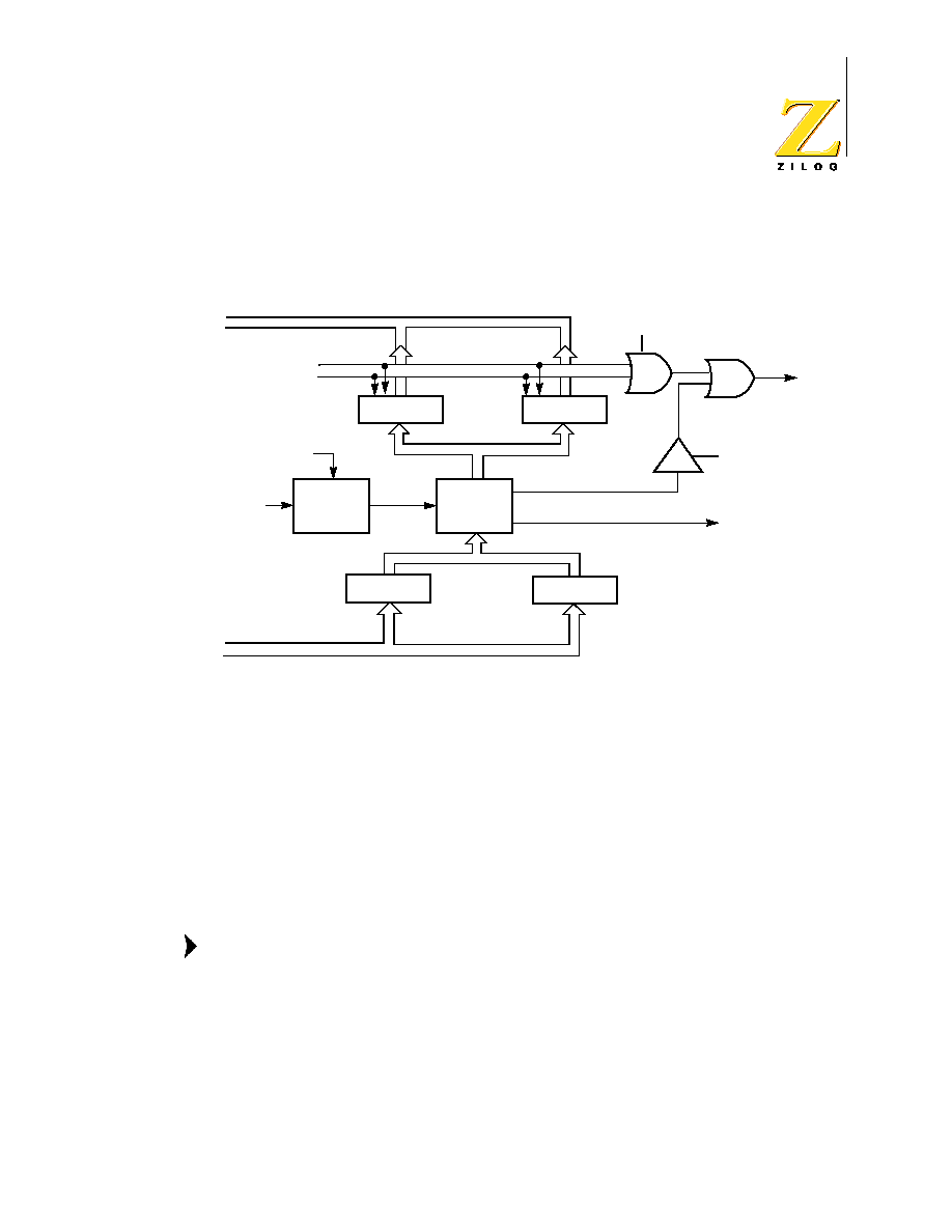
Z86D86
28-Pin Low-Voltage OTP Microcontroller
PS008904-1003
P R E L I M I N A R Y
50
Sixteen-Bit Counter/Timer Circuits
Figure 39 shows the 16-bit counter/timer circuits.
Figure 39. 16-Bit Counter/Timer Circuits
T16 Transmit Mode
In Normal or Ping-Pong Mode, the output of T16, when not enabled, is dependent
on CTR1, D0. If the result is a 0, T16_OUT is a 1; if it is a 1, T16_OUT is 0. You
can force the output of T16 to either a 0 or 1 whether it is enabled or not by pro-
gramming CTR1 D3, D2 to a 10 or 11.
When T16 is enabled, TC16H * 256 + TC16L is loaded, and T16_OUT is switched
to its initial value (CTR1, D0). When T16 counts down to 0, T16_OUT is toggled
(in Normal or Ping-Pong Mode), an interrupt is generated if enabled (CTR2, D1),
and a status bit (CTR2, D5) is set.
Global interrupts override this function as described in
"Interrupts" on page 54.
If T16 is in Single-Pass Mode, T16 is stopped at this point (see Figure 40). If T16
is in Modulo-N Mode, T16 is loaded with TC16H * 256 + TC16L and the counting
continues (see Figure 41).
Z8 Data Bus
Pos Edge
Neg Edge
CTR2 D4, D3
SCLK
Z8 Data Bus
Clock
Select
Clock
16-Bit
Counter
TC16H
TC16L
CTR2 D2
IRQ3
CTR2 D1
T16_OUT
HI16
LO16
T16
Note:
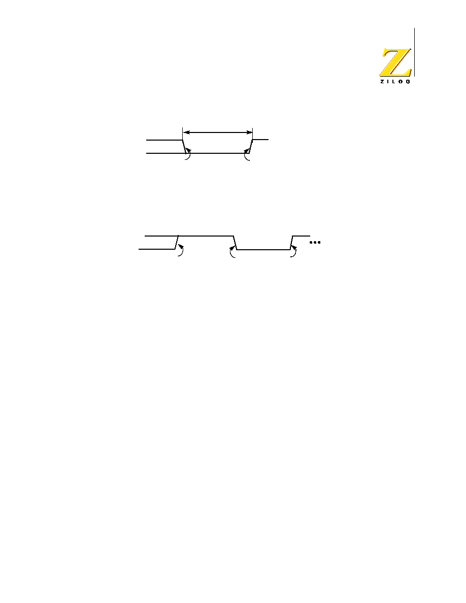
Z86D86
28-Pin Low-Voltage OTP Microcontroller
PS008904-1003
P R E L I M I N A R Y
51
Figure 40. T16_OUT in Single-Pass Mode
Figure 41. T16_OUT in Modulo-N Mode
You can modify the values in TC16H and TC16L at any time. The new values take
effect when they are loaded. To ensure known operation, do not load these regis-
ters at the time the values are to be loaded into the counter/timer. An initial count
of 1 is not allowed. An initial count of 0 causes T16 to count from 0 to FFFFh to
FFFEh. Transition from 0 to FFFFh is not a time-out condition.
T16 Demodulation Mode
You need to program TC16L and TC16H to FFh. After T16 is enabled, when the
first edge (rising, falling, or both, depending on CTR1 D5, D4) is detected, T16
captures HI16 and LO16, reloads, and begins counting.
If D6 of CTR2 Is 0
When a subsequent edge (rising, falling, or both, depending on CTR1, D5, D4) is
detected during counting, the current count in T16 is one's complemented and put
into HI16 and LO16. When data is captured, one of the edge-detect status bits
(CTR1, D1, D0) is set, and an interrupt is generated if enabled (CTR2, D2). From
that point, T16 is loaded with FFFFh and starts again.
This T16 mode is generally used to measure mark time, defined as the length of
time between carrier signal bursts (marks).
TC16H*256+TC16L Counts
Counter Enable Command,
T16_OUT switches to its
initial value (CTR1 D0)
T16_OUT toggles
Time-out Interrupt
T16_OUT
TC16H*256+TCl16
Counter Enable Command,
T16_OUT switches to its
initial value (CTR1 D0)
T16_OUT Toggles,
Time-out Interrupt
T16_OUT Toggles,
Time-out Interrupt
TC16H*256+TCl16
TC16H*256+TCl16

Z86D86
28-Pin Low-Voltage OTP Microcontroller
PS008904-1003
P R E L I M I N A R Y
52
If D6 of CTR2 Is 1
T16 ignores the subsequent edges in the input signal and continues counting
down. A time-out of T8 causes T16 to capture its current value and generate an
interrupt if enabled (CTR2, D2). In this case, T16 does not reload and continues
counting. If the D6 bit of CTR2 is toggled (by writing a 0 and then a 1 to it), T16
captures and reloads on the next edge (rising, falling, or both, depending on
CTR1, D5, D4), thereby continuing to ignore subsequent edges.
This T16 mode is generally used to measure mark time, defined by the length of
time between active carrier signal bursts (marks).
When T16 reaches 0, it continues counting from FFFFh. Meanwhile, a status bit
(CTR2, D5) is set, and an interrupt time-out can be generated if enabled (CTR2,
D1).
Ping-Pong Mode
This operation mode (see Figure 42) is only valid in transmit mode. T8 and T16
must be programmed in Single-Pass Mode (CTR0, D6; CTR2, D6), and Ping-
Pong Mode must be programmed in CTR1, D3, D2. You can begin the operation
by enabling either T8 or T16 (CTR0, D7 or CTR2, D7). For example, if T8 is
enabled, T8_OUT is set to this initial value (CTR1, D1). According to T8_OUT's
level, TC8H or TC8L is loaded into T8. After the terminal count is reached, T8 is
disabled, and T16 is enabled. T16_OUT switches to its initial value (CTR1, D0),
data from TC16H and TC16L is loaded, and T16 starts to count. After T16 reaches
the terminal count, it stops, T8 is enabled again, and the entire cycle repeats.
Interrupts can be allowed when T8 or T16 reaches terminal control (CTR0, D1;
CTR2, D1). To stop the Ping-Pong operation, write 00 to bits D3 and D2 of CTR1.
Enabling Ping-Pong operation while the counter/timers are
running might cause intermittent counter/timer function. Disable
the counter/timers and then reset the status flags before
instituting this operation.
Note:

Z86D86
28-Pin Low-Voltage OTP Microcontroller
PS008904-1003
P R E L I M I N A R Y
53
Figure 42. Ping-Pong Mode
Starting Ping-Pong Mode
First, make sure both counter/timers are not running. Then set T8 into Single-
Pass Mode (CTR0, D6), set T16 into Single-Pass Mode (CTR2, D6), and set the
Ping-Pong Mode (CTR1, D2, D3). These instructions do not have to be in any par-
ticular order. Finally, start Ping-Pong Mode by enabling either T8 (CTR0, D7) or
T16 (CTR2, D7).
During Ping-Pong Mode
The enable bits of T8 and T16 (CTR0, D7; CTR2, D7) are set and cleared alter-
nately by hardware. The time-out bits (CTR0, D5; CTR2, D5) are set every time
the counter/timers reach the terminal count.
Enable
TC8
Time-out
Enable
TC16
Time-out
Ping-Pong
CTR1, D3, D2

Z86D86
28-Pin Low-Voltage OTP Microcontroller
PS008904-1003
P R E L I M I N A R Y
54
Output Circuit
Figure 43 shows the output circuit.
Figure 43. Output Circuit
Interrupts
The Z86D86 features six different interrupts. The interrupts are maskable and pri-
oritized, as shown in Figure 44. The six sources are divided as follows: three
sources are claimed by Port 3 lines P33≠P31, two by the counter/timers, and one
by LBD (seeTable 21). The Interrupt Mask Register, globally or individually,
enables or disables the six interrupt requests.
MUX
MUX
MUX
MUX
AND/OR/NOR/NAND
Logic
T8_OUT
T16_OUT
CTR1 D2
CTR1 D3
CTR1 D5, D4
P35_INTERNAL
CTR2 D0
P35
CTR1 D6
P36
CTR0 D0
P36_INTERNAL
P34
P34_INTERNAL
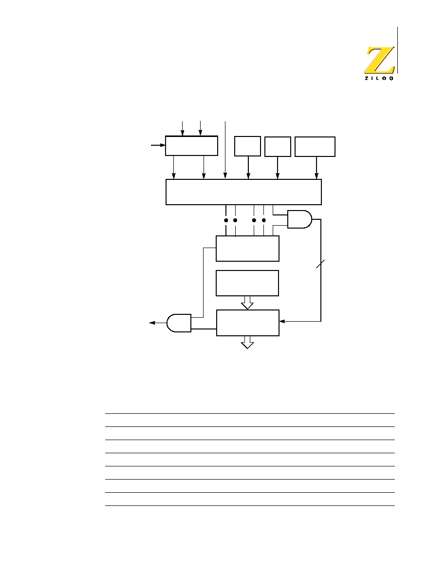
Z86D86
28-Pin Low-Voltage OTP Microcontroller
PS008904-1003
P R E L I M I N A R Y
55
Figure 44. Interrupt Block Diagram
Table 21. Interrupt Types, Sources, and Vectors
Name
Source
Vector Location Comments
IRQ0
P32
0,1
External (P32), Rising Falling Edge Triggered
IRQ1
P33
2,3
External (P33), Falling Edge Triggered
IRQ2
P31, T
IN
4,5
External (P31), Rising Falling Edge Triggered
IRQ3
T16
6,7
Internal
IRQ4
T8
8,9
Internal
IRQ5
LBD
10,11
Internal
P31 P32
P33
IRQ Register
D6, D7
Interrupt
Edge Select
Timer
Timer
Low Battery
IRQ2
IMR
Global
Interrupt
Enable
Interrupt
Request
Vector Select
16
8
Detection
5
IRQ0 IRQ1
IRQ3
IRQ4
IRQ5
IPR
Priority
Logic
IRQ

Z86D86
28-Pin Low-Voltage OTP Microcontroller
PS008904-1003
P R E L I M I N A R Y
56
When more than one interrupt is pending, priorities are resolved by a programma-
ble priority encoder controlled by the Interrupt Priority Register. An interrupt
machine cycle is activated when an interrupt request is granted. As a result, all
subsequent interrupt are disabled, and the Program Counter and Status Flags are
saved. The cycle then branches to the program memory vector location reserved
for that interrupt. All Z86D86 interrupts are vectored through locations in the pro-
gram memory. This memory location and the next byte contain the 16-bit address
of the interrupt service routine for that particular interrupt request. To accommo-
date polled interrupt systems, interrupt inputs are masked, and the Interrupt
Request register is polled to determine which of the interrupt requests require ser-
vice.
An interrupt resulting from AN1 is mapped into IRQ2, and an interrupt from AN2 is
mapped into IRQ0. Interrupts IRQ2 and IRQ0 can be rising, falling, or both edge
triggered; all are programmable by the user. The software can poll to identify the
state of the pin.
Programming bits for the Interrupt Edge Select are located in the IRQ Register
(R250), bits D7 and D6. The configuration is indicated in Table 22.
Clock
The Z86D86 on-chip oscillator has a high-gain, parallel-resonant amplifier for con-
nection to a crystal, LC, ceramic resonator, or any suitable external clock source
(XTAL1 = Input, XTAL2 = Output). The crystal must be AT cut, 1 MHz to 8 MHz
maximum, with a series resistance (RS) less than or equal to 100 Ohms. The
Z86D86 on-chip oscillator can be driven with a low-cost RC network or other suit-
able external clock source.
Table 22. IRQ Register*
IRQ
Interrupt Edge
D7
D6
IRQ2 (P31)
IRQ0 (P32)
0
0
F
F
0
1
F
R
1
0
R
F
1
1
R/F
R/F
Notes:
F = Falling Edge
R = Rising Edge
*In stop mode, the comparators are turned off.
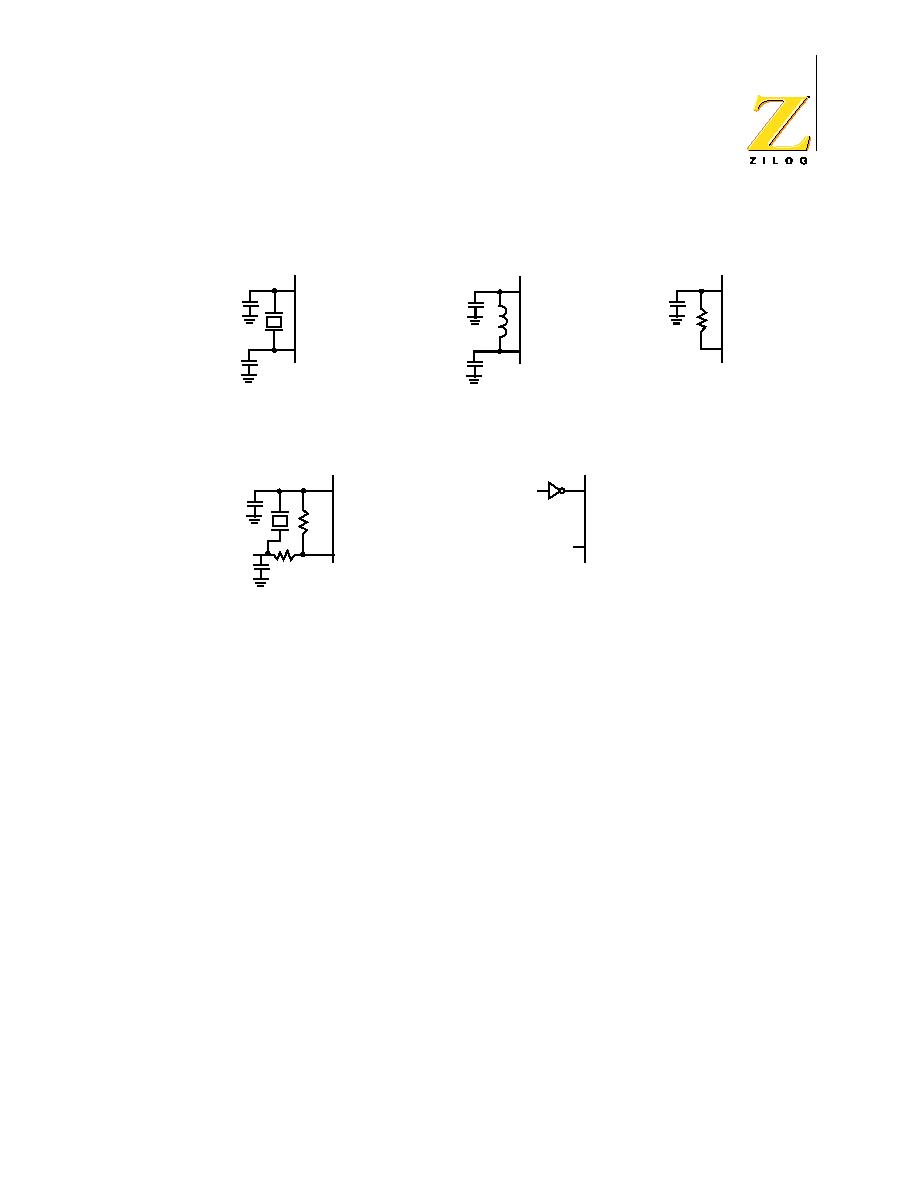
Z86D86
28-Pin Low-Voltage OTP Microcontroller
PS008904-1003
P R E L I M I N A R Y
57
For 32-kHz crystal operation, an external feedback resistor (Rf) and a serial resis-
tor (Rd) are required. See Figure 45.
Figure 45. Oscillator Configuration
The crystal needs to be connected across XTAL1 and XTAL2 using the recom-
mended capacitors (capacitance greater than or equal to 22 pF) from each pin to
ground. The RC oscillator configuration is an external resistor connected from
XTAL1 to XTAL2, with a frequency-setting capacitor from XTAL1 to ground (see
Figure 45).
Power-On Reset (POR)
A timer circuit clocked by a dedicated on-board RC oscillator is used for the
Power-On Reset (POR) timer function. The POR time allows V
CC
and the oscilla-
tor circuit to stabilize before instruction execution begins.
The POR timer circuit is a one-shot timer triggered by one of three conditions:
∑
Power Fail to Power OK status including waking up from V
LV
Standby
∑
Stop-Mode Recovery (if D5 of SMR = 1)
∑
WDT Time-Out
C1
C2
XTAL1
XTAL2
L
R
Rf
Rd
C1
C1
C1
C2
C2
XTAL1
XTAL2
XTAL1
XTAL2
XTAL1
XTAL2
XTAL1
XTAL2
Ceramic Resonator or Crystal
C1, C2 = 47pF TYP*
f = 8 MHz
LC
C1, C2 = 22 pF
L = 130
µ
H*
f = 3 MHz*
RC
@ 3V VCC (TYP)
C1 = 33 pF*
R = 1K*
32 kHz XTAL
C1 = 20 pF, C = 33 pF
Rd = 56≠470K
Rf = 10M
External Clock
* Preliminary value including pin parasitics

Z86D86
28-Pin Low-Voltage OTP Microcontroller
PS008904-1003
P R E L I M I N A R Y
58
The POR time is a nominal 5 ms. Bit 5 of the Stop-Mode Register determines
whether the POR timer is bypassed after Stop-Mode Recovery (typical for external
clock, RC, and LC oscillators).
HALT
HALT turns off the internal CPU clock, but not the XTAL oscillation. The counter/
timers and external interrupts IRQ0, IRQ1, IRQ2, IRQ3, and IRQ4 remain active.
The devices are recovered by interrupts, either externally or internally generated.
An interrupt request must be executed (enabled) to exit HALT Mode. After the
interrupt service routine, the program continues from the instruction after the
HALT.
STOP
This instruction turns off the internal clock and external crystal oscillation and
reduces the standby current to 10 µA or less. STOP Mode is terminated only by a
reset (such as WDT time-out), POR, SMR, or external reset. This termination
causes the processor to restart the application program at address 000CH. To
enter STOP (or HALT) mode, you need to first flush the instruction pipeline to
avoid suspending execution in mid-instruction. To execute this action, you must
execute a NOP (op code = FFH) immediately before the appropriate sleep instruc-
tion. For example:
FF
NOP
; clear the pipeline
6F
STOP
; enter STOP Mode
or
FF
NOP
; clear the pipeline
7F
HALT
; enter HALT Mode
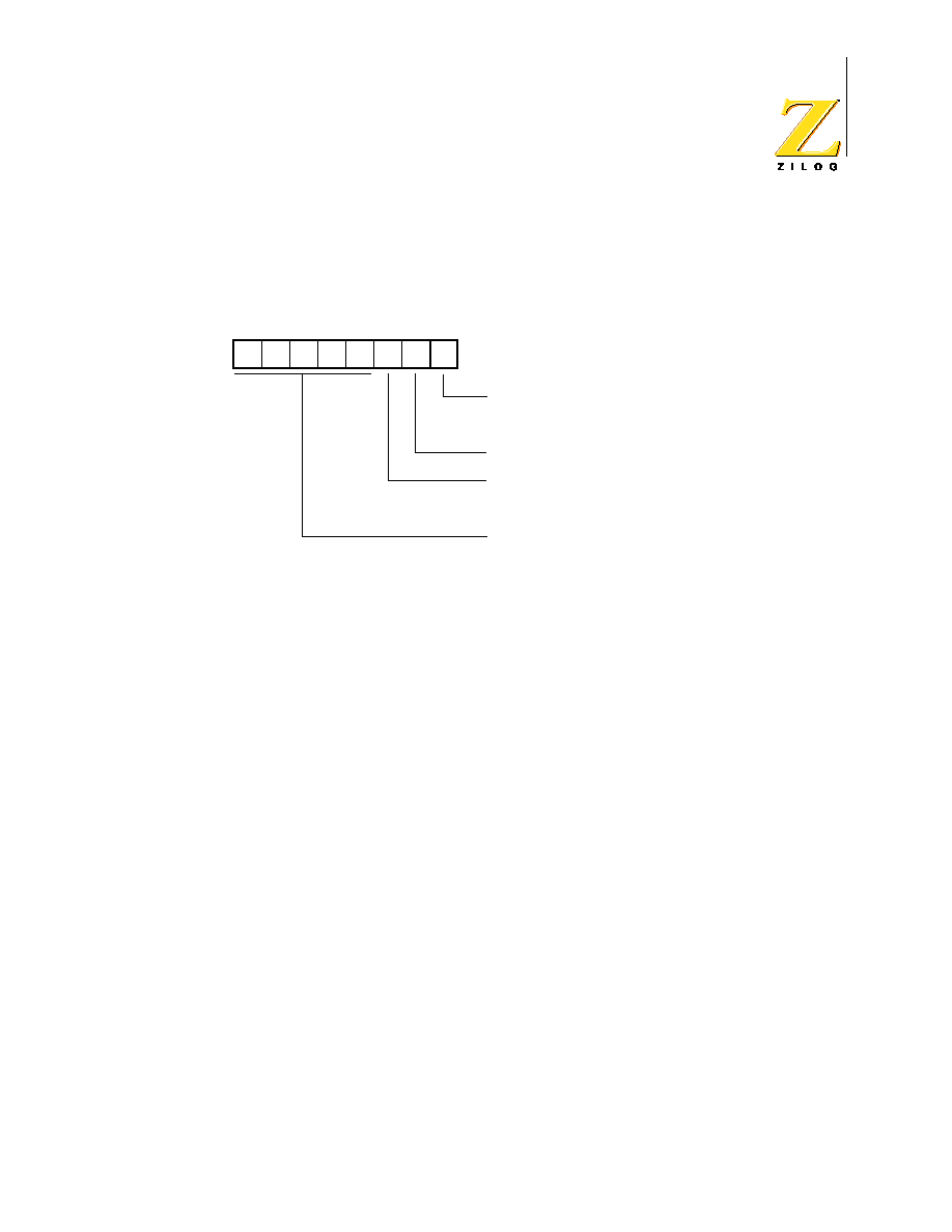
Z86D86
28-Pin Low-Voltage OTP Microcontroller
PS008904-1003
P R E L I M I N A R Y
59
Port Configuration Register (PCON)
The PCON register configures the comparator output on Port 3. It is located in the
expanded register 2 at Bank F, location 00, as shown in Figure 46.
Figure 46. Port Configuration Register (PCON)--Write Only
Comparator Output Port 3 (D0)
Bit 0 controls the comparator used in Port 3. A 1 in this location brings the compar-
ator outputs to P34 and P37, and a 0 releases the port to its standard (/O configu-
ration.
Port 0 Output Mode (D2)
Bit 2 controls the output mode of Port 0. A 1 in this location sets the output to
push-pull, and a 0 sets the output to open-drain.
Stop-Mode Recovery Register (SMR)
This register selects the clock divide value and determines the mode of Stop-
Mode Recovery (Figure 47). All bits are write only except bit 7, which is read only.
Bit 7 is a flag bit that is hardware set on the condition of STOP recovery and reset
by a power-on cycle. Bit 6 controls whether a low level or a high level at the XOR-
gate input is required from the recovery source. Bit 5 controls the reset delay after
recovery. Bits D2, D3, and D4, or the SMR register, specify the source of the Stop-
Mode Recovery signal. Bit D0 determines if SCLK/TCLK (shown in Figure 48) are
divided by 16 or not. The SMR is located in Bank F of the Expanded Register
Group at address 0BH.
D7 D6 D5 D4 D3 D2 D1 D0
Comparator Output Port 3
Reserved (must be 1)
Port 0
0 = Open-drain
1 = Push-pull*
Reserved (must be 1)
*Default setting after reset
PCON (FH) 00H
0 P34, P37, Standard Output*
1 P34, P37, Comparator Output

Z86D86
28-Pin Low-Voltage OTP Microcontroller
PS008904-1003
P R E L I M I N A R Y
60
Figure 47. Stop-Mode Recovery Register
Figure 48. SCLK Circuit
D7 D6 D5 D4 D3 D2 D1 D0
SCLK/TCLK Divide-by-16
0 = OFF **
1 = ON
Reserved (must be 0)
Stop-Mode Recovery Source
000 = POR Only *
001 = Reserved
010 = P31
011 = P32
100 = P33
101 = P27
110 = P2 NOR 0≠3
111 = P2 NOR 0≠7
Stop Delay
Reserved (must be 1)
1 = ON *
Stop Recovery Level ***
0 = Low *
1 = High
Stop Flag
0 = POR *
1 = Stop Recovery **
* Default setting after reset
** Default setting after reset and Stop-Mode Recovery
*** At the XOR gate input
SMR (0F) 0B
OSC
Divide
by 2
Divide
by 16
SCLK
TCLK
SMR, D0

Z86D86
28-Pin Low-Voltage OTP Microcontroller
PS008904-1003
P R E L I M I N A R Y
61
SCLK/TCLK Divide-by-16 Select (D0)
D0 of the SMR controls a Divide-by-16 prescaler of SCLK/TCLK. The purpose of
this control is to selectively reduce device power consumption during normal pro-
cessor execution (SCLK control) and/or HALT Mode (where TCLK sources inter-
rupt logic). After Stop-Mode Recovery, this bit is set to a 0.
Stop-Mode Recovery Source (D2, D3, and D4)
These three bits of the SMR specify the wake-up source of the STOP recovery
(Figure 49 and Table 23 on page 63).
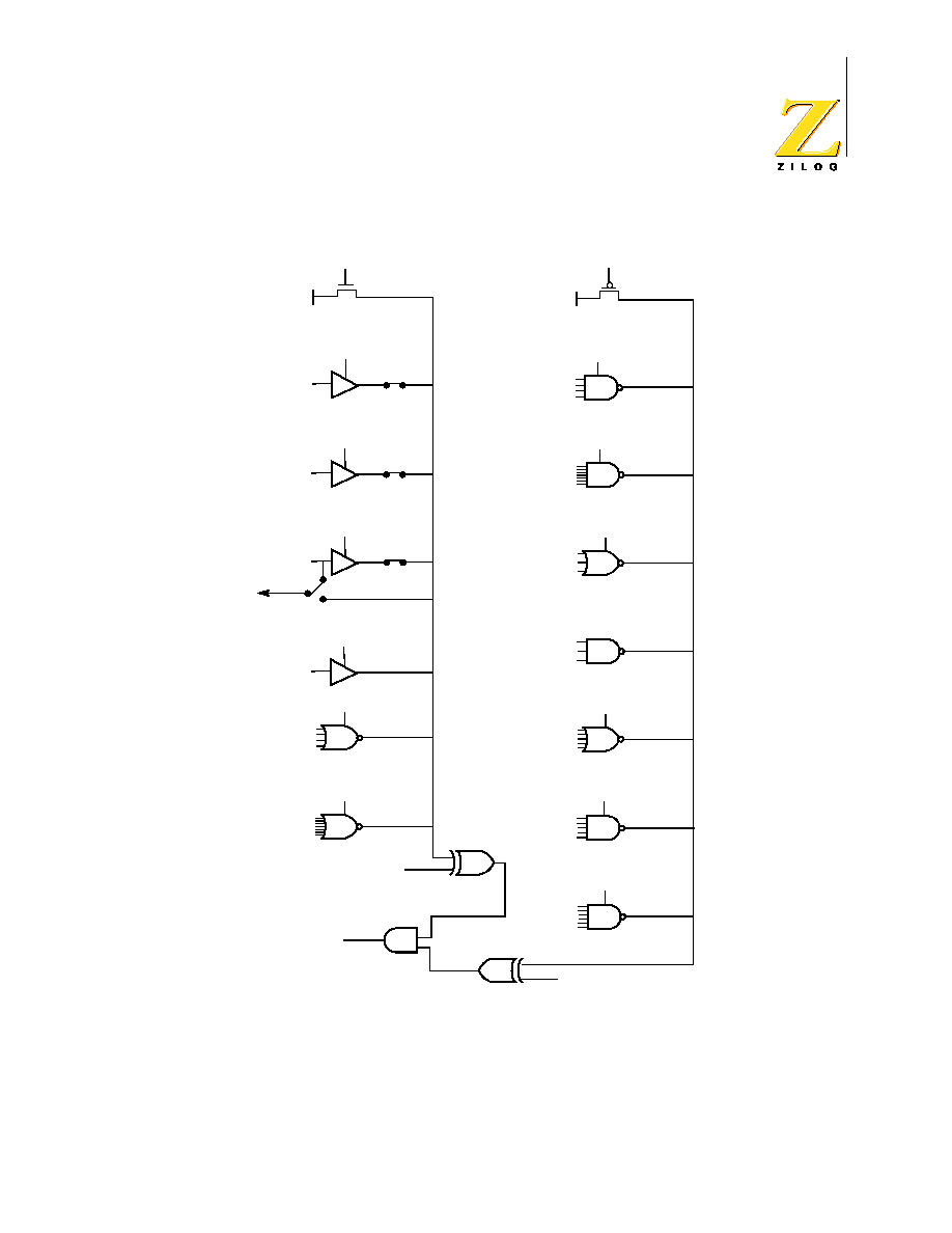
Z86D86
28-Pin Low-Voltage OTP Microcontroller
PS008904-1003
P R E L I M I N A R Y
62
Figure 49. Stop-Mode Recovery Source
SMR D4 D3 D2
V
CC
P31
P32
P33
To IRQ1
S3
S4
P27
P20
P23
P20
P27
SMR D6
0 0
0
SMR D4 D3 D2
1 0
0
SMR D4 D3 D2
1 1
1
SMR D4 D3 D2
1 0
1
SMR D4 D3 D2
0 1
1
SMR D4 D3 D2
0 0
1
SMR D4 D3 D2
1 1
0
SMR D4 D3 D2
1 0
0
SMR D4 D3 D2
0 1
0
SMR D4 D3 D2
0 0
0
SMR D4 D3 D2
1 1
1
SMR D4 D3 D2
1 0
1
SMR D4 D3 D2
0 1
1
SMR D4 D3 D2
0 0
1
SMR D4 D3 D2
1 1
0
S1
S2
SMR2 D6
P20
P23
P20
P27
P31
P32
P33
P31
P32
P33
P31
P32
P33
P00
P07
P31
P32
P33
P20
P21
P22
P31
P32
P33
P00
P07
V
CC
To RESET and WDT
Circuitry (Active Low)

Z86D86
28-Pin Low-Voltage OTP Microcontroller
PS008904-1003
P R E L I M I N A R Y
63
Any Port 2 bit defined as an output drives the corresponding
input to the default state to allow the remaining inputs to control
the AND/OR function. Refer to "Stop-Mode Recovery Register
2 (SMR2)" on page 64 for other recover sources.
Stop-Mode Recovery Delay Select (D5)
This bit, if low, disables the 5-ms RESET delay after Stop-Mode Recovery. The
default configuration of this bit is one. If the "fast" wake up is selected, the Stop-
Mode Recovery source must be kept active for at least 5TpC.
Stop-Mode Recovery Edge Select (D6)
A 1 in this bit position indicates that a High level on any one of the recovery
sources wakes the Z86D86 from STOP Mode. A 0 indicates Low level recovery.
The default is 0 on POR.
Cold or Warm Start (D7)
This bit is read only. It is set to 1 when the device is recovered from stop mode.
The bit is set to 0 when the device reset is other than Stop-Mode Recovery
(SMR).
Table 23. Stop-Mode Recovery Source
SMR:432
Operation
D4
D3
D2
Description of Action
0
0
0
POR and/or external reset recovery
0
0
1
Reserved
0
1
0
P31 transition
0
1
1
P32 transition
1
0
0
P33 transition
1
0
1
P27 transition
1
1
0
Logical NOR of P20 through P23
1
1
1
Logical NOR of P20 through P27
Note:
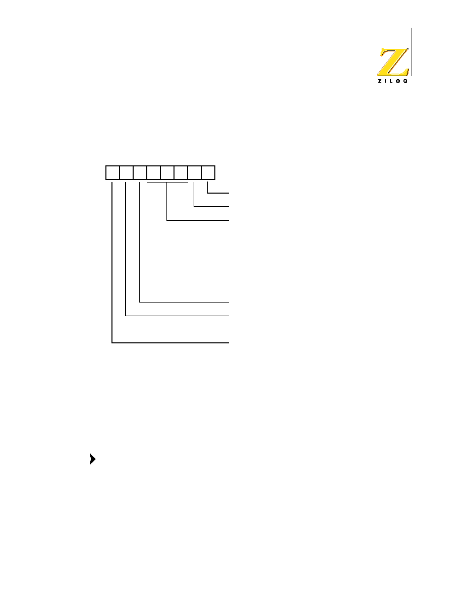
Z86D86
28-Pin Low-Voltage OTP Microcontroller
PS008904-1003
P R E L I M I N A R Y
64
Stop-Mode Recovery Register 2 (SMR2)
This register determines the mode of Stop-Mode Recovery for SMR2 (see
Figure 50).
Figure 50. Stop-Mode Recovery Register 2--(0F) DH:D2≠D4, D6 Write Only
If SMR2 is used in conjunction with SMR, either of the specified events causes a
Stop-Mode Recovery.
Port pins configured as outputs are ignored as a SMR or SMR2
recovery source. For example, if the NAND or P23≠P20 is
selected as the recovery source and P20 is configured as an
output, the remaining SMR pins (P23≠P21) form the NAND
equation.
Table 24 describes the contents of the Stop-Mode Recovery register 2.
D7 D6 D5 D4 D3 D2 D1 D0
Reserved (must be 0)
Reserved (must be 0)
Stop-Mode Recovery Source 2
000 = POR Only *
001 = NAND P20, P21, P22, P23
010 = NAND P20, P21, P22, P33, P24, P25, P26, P27
011 = NOR P31, P32, P33
100 = NAND P31, P32, P33
101 = NOR P31, P32, P33, P00, P07
110 = NAND P31, P32, P33, P00, P07
111 = NAND P31, P32, P33, P20, P21, P22
Reserved (must be 0)
Recovery Level **
0 = Low *
1 = High
* Default setting after reset
** At the XOR gate input
Reserved (must be 0)
SMR2 (0F) DH
Note: If used in conjunction with SMR,
either of the two specified events
causes a Stop-Mode Recovery.
Note:

Z86D86
28-Pin Low-Voltage OTP Microcontroller
PS008904-1003
P R E L I M I N A R Y
65
Watch-Dog Timer Mode Register (WDTMR)
The WDT is a retriggerable, one-shot timer that resets the Z8 if it reaches its ter-
minal count. The WDT must initially be enabled by executing the WDT instruction.
On subsequent executions of the WDT instruction, the WDT circuit is refreshed.
The WDT circuit is driven by an on-board RC oscillator or external oscillator from
the XTAL1 pin. The WDT instruction affects the Zero (Z), Sign (S), and Overflow
(V) flags.
The POR clock source is selected with bit 4 of the WDT register. Bits 0 and 1 con-
trol a tap circuit that determines the minimum time-out period. Bit 2 determines
whether the WDT is active during HALT, and Bit 3 determines WDT activity during
STOP. Bits 5 through 7 are reserved (Figure 51). This register is accessible only
during the first 60 processor cycles (122 XTAL clocks) from the execution of the
first instruction after Power-On-Reset, Watch-Dog Reset, or a Stop-Mode Recov-
ery (Figure 51). After this point, the register cannot be modified by any means,
intentional or otherwise. The WDTMR cannot be read. The register is located in
Bank F of the Expanded Register Group at address location 0FH. The WDTMR is
organized as shown in Figure 51.
Table 24. SMR2(F)0Dh: Stop-Mode Recovery Register 2
Field
Bit Position
Value
Description
Reserved
7-------
0
Reserved (Must be 0)
Recovery Level
-6------
W
0*
1
Low
High
Reserved
--5-----
0
Reserved (Must be 0)
Source
---432--
W
000*
001
010
011
100
101
110
111
A. POR Only
B. NAND of P23≠P20
C. NAND or P27≠P20
D. NOR of P33≠P31
E. NAND of P33≠P31
F. NOR of P33≠P31, P00, P07
G. NAND of P33≠P31, P00, P07
H. NAND of P33≠P31, P22≠P20
Reserved
------10
00
Reserved (Must be 0)
Notes:
*Indicates the value upon Power-On Reset
Port pins configured as outputs are ignored as a SMR recovery source.

Z86D86
28-Pin Low-Voltage OTP Microcontroller
PS008904-1003
P R E L I M I N A R Y
66
Figure 51. Watch-Dog Timer Mode Register--Write Only
WDT Time Select (D0, D1)
This bit selects the WDT time period. It is configured as indicated in Table 25.
WDTMR During HALT (D2)
This bit determines whether or not the WDT is active during HALT Mode. A 1 indi-
cates active during HALT. The default is 1.
Table 25. WDT Time Select*
D1
D0
Time-Out of Internal RC OSC
Time-Out of XTAL Clock
0
0
5 ms min
256 TpC
0
1
10 ms min
512 TpC
1
0
20 ms min
1024 TpC
1
1
80 ms min
4096 TpC
Notes:
*TpC = XTAL clock cycle. The default on reset is 10 ms.
D7 D6 D5 D4 D3 D2 D1 D0
WDT TAP INT RC OSC External Clock
* Default setting after reset
00 5 ms min 256 TpC
01* 10 ms min 512 TpC
10 20 ms min 1024 TpC
11 80 ms min 4096 TpC
WDT during HALT
0 = OFF
1 = ON*
WDT during STOP
0 = OFF
1 = ON*
Reserved (must be 0)
WDTMR (0F) 0F
XTAL/INT RC Select for WDT
0 = RC OSC
1 = XTAL
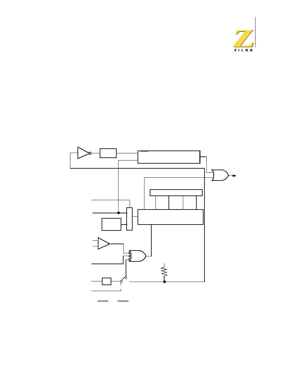
Z86D86
28-Pin Low-Voltage OTP Microcontroller
PS008904-1003
P R E L I M I N A R Y
67
WDTMR During STOP (D3)
This bit determines whether or not the WDT is active during STOP Mode. Since
the XTAL clock is stopped during STOP Mode, the on-board RC has to be
selected as the clock source to the WDT/POR counter. A 1 indicates active during
STOP. The default is 1.
Clock Source for WDT (D4)
This bit determines which oscillator source is used to clock the internal POR and
WDT counter chain. If the bit is a 1, the internal RC oscillator is bypassed, and the
POR and WDT clock source is driven from the external pin, XTAL1. The default
configuration of this bit is 0, which selects the RC oscillator. See Figure 51.
Figure 51. Resets and WDT
+
≠
5 Clock
Filter
*
CLR2
CLK
18 Clock Reset
Generator
Reset
Internal
Reset
Active
High
WDT
TAP SELECT
Ck source
Select
(WDTMR)
XTAL
Internal
RD OSC.
M
U
X
POR
10 ms
20 ms
80 ms
5 ms
CLK
*CLR1
WDT/POR Counter Chain
V
DD
VBO/VLV
2V Ref.
WDT
From Stop Mode
Recovery Source
12 ns Glitch Filter
Stop Delay
Select (SMR)
V
CC
Low Operating
Voltage Det.
256 TpC 512 TpC 1024 TpC 4096 TpC
*CLR1 and CLR2 enable the WDT/POR and
18 Clock Reset timers upon a Low-to-High input translation.

Z86D86
28-Pin Low-Voltage OTP Microcontroller
PS008904-1003
P R E L I M I N A R Y
68
Mask Selectable Options
There are six Mask Selectable Options to choose from based on ROM code
requirements. These are listed in Table 26.
Low Voltage/Standby
An on-chip Voltage Comparator checks that the V
CC
is at the required level for
correct operation of the device. Reset is globally driven when V
CC
falls below V
LV
.
A further small drop in V
CC
causes the XTAL1 and XTAL2 circuitry to stop the
crystal or resonator clock. Typical low-voltage power consumpion in this Low Volt-
age Standby mode (I
LV
) is about 100 µA. If the V
CC
is allowed to stay above Vram,
the RAM content is preserved. When the power level is returned to above V
LV
, the
device performs a POR and functions normally.
Low Battery Detection and Flag
A Low Battery Detection circuit can be used to signal dropping voltage levels.
Expanded Register Bank 0Dh register 0Ch bit 0 and 1 are used for this option.
Bit D0 is used to enable/disable this function.
Bit D1 is the status flag bit of this LBD.
The minimum operating voltage varies with the temperature and operating fre-
quency, while VLV varies with temperature only.
Table 26. Mask Selectable Options
RC/Other
RC/XTAL
32 kHz XTAL
On/Off
Port 04≠07 Pull-Ups
On/Off
Port 00≠03 Pull-Ups
On/Off
Port 20≠27 Pull-Ups
On/Off
Port 0:0≠3 Mouse Mode 0.4 V
CC
Trip
On/Off

Z86D86
28-Pin Low-Voltage OTP Microcontroller
PS008904-1003
P R E L I M I N A R Y
69
Ordering Information
Figure 52 shows the 28-pin SOIC package diagram. Figure 53 shows the 28-pin
DIP package diagram.
Figure 52. 28-Pin SOIC Package Diagram

Z86D86
28-Pin Low-Voltage OTP Microcontroller
PS008904-1003
P R E L I M I N A R Y
70
Figure 53. 28-Pin DIP Package Diagram
Z86D86 8.0 MHz
For fast results, contact your local ZiLOG sales office for assistance in ordering
the part desired.
28-Pin DIP
Z86D8608PSC
28-Pin SOIC
Z86D8608SSC

Z86D86
28-Pin Low-Voltage OTP Microcontroller
PS008904-1003
P R E L I M I N A R Y
71
Codes
Figure 54 shows an example of what the ordering codes represent.
Figure 54. Ordering Codes Example
Package
P = Plastic DIP
S = SOIC
Temperature
S = 0 ∞C to +70 ∞C
Speed
8 = 8.0 MHz
Environmental
C = Plastic Standard
Precharacterization Product
The product represented by this document is newly introduced and ZiLOG has not
completed the full characterization of the product. The document states what
ZiLOG knows about this product at this time, but additional features or nonconfor-
mance with some aspects of the document may be found, either by ZiLOG or its
customers in the course of further application and characterization work. In addi-
tion, ZiLOG cautions that delivery may be uncertain at times, due to startup yield
issues.
Example:
Z 86D86 08 P S
C
is a Z86D86, 8 MHz, DIP, 0 ∞C to 70 ∞C, Plastic Standard Flow
Environmental Flow
Temperature
Package
Speed
Product Number
ZiLOG Prefix

Z86D86
28-Pin Low-Voltage OTP Microcontroller
PS008904-1003
P R E L I M I N A R Y
72
Customer Feedback Form
Z86D86 28-Pin Low-Voltage OTP Microcontroller
If you experience any problems while operating this product, or if you note any inaccura-
cies while reading this product specification, please copy and complete this form, then
mail or fax it to ZiLOG (see Return Information, below). We also welcome your sugges-
tions!
Customer Information
Product Information
Return Information
ZiLOG
System Test/Customer Support
532 Race Street
San Jose, CA 95126-3432
Fax: (408) 558-8300
Problem Description or Suggestion
Provide a complete description of the problem or your suggestion. If you are reporting a
specific problem, include all steps leading up to the occurrence of the problem. Attach
additional pages as necessary.
_______________________________________________________________________________
_______________________________________________________________________________
_______________________________________________________________________________
Name
Country
Company
Phone
Address
Fax
City/State/Zip
email
Serial # or Board Fab #/Rev #
Software Version
Document Number
Host Computer Description/Type