 | –≠–ª–µ–∫—Ç—Ä–æ–Ω–Ω—ã–π –∫–æ–º–ø–æ–Ω–µ–Ω—Ç: Z86E0412 | –°–∫–∞—á–∞—Ç—å:  PDF PDF  ZIP ZIP |
DS97Z8X0401
P R E L I M I N A R Y
1
1
P
RELIMINARY
P
RODUCT
S
PECIFICATION
Z86E04/E08
1
CMOS Z8 OTP M
ICROCONTROLLERS
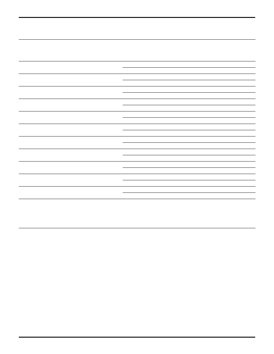
PRODUCT DEVICES
Several key product features of the extensive family of Zilog Z86E04/E08 CMOS OTP microcontrollers are presented in
the above table. This table enables the user to identify which of the twenty E04/E08 product variants most closely match
the user's application requirements.
Part
Oscillator
Operating
Operating
ROM
Number
Type
V
CC
Temperature
(KB)
Package
Z86E0412PEC
Crystal
4.5V - 5.5V
-40
∞
C/105
∞
C
1
18-Pin DIP
Z86E0412PSC1860
Crystal
3.0V - 5.5V
0
∞
C/70
∞
C
1
18-Pin DIP
Z86E0412PSC1866
Crystal
4.5V - 5.5V
0
∞
C/70
∞
C
1
18-Pin DIP
Z86E0412PSC1903
RC
4.5V - 5.5V
0
∞
C/70
∞
C
1
18-Pin DIP
Z86E0412PSC1924
RC
3.0V - 5.5V
0
∞
C/70
∞
C
1
18-Pin DIP
Z86E0412SEC
Crystal
4.5V - 5.5V
-40
∞
C/105
∞
C
1
18-Pin SOIC
Z86E0412SSC1860
Crystal
3.0V - 5.5V
0
∞
C/70
∞
C
1
18-Pin SOIC
Z86E0412SSC1866
Crystal
4.5V - 5.5V
0
∞
C/70
∞
C
1
18-Pin SOIC
Z86E0412SSC1903
RC
4.5V - 5.5V
0
∞
C/70
∞
C
1
18-Pin SOIC
Z86E0412SSC1924
RC
3.0V - 5.5V
0
∞
C/70
∞
C
1
18-Pin SOIC
Z86E0812PEC
Crystal
4.5V - 5.5V
-40
∞
C/105
∞
C
2
18-Pin DIP
Z86E0812PSC1860
Crystal
3.0V - 5.5V
0
∞
C/70
∞
C
2
18-Pin DIP
Z86E0812PSC1866
Crystal
4.5V - 5.5V
0
∞
C/70
∞
C
2
18-Pin DIP
Z86E0812PSC1903
RC
4.5V - 5.5V
0
∞
C/70
∞
C
2
18-Pin DIP
Z86E0812PSC1924
RC
3.0V - 5.5V
0
∞
C/70
∞
C
2
18-Pin DIP
Z86E0812SEC
Crystal
4.5V - 5.5V
-40
∞
C/105
∞
C
2
18-Pin SOIC
Z86E0812SSC1860
Crystal
3.0V - 5.5V
0
∞
C/70
∞
C
2
18-Pin SOIC
Z86E0812SSC1866
Crystal
4.5V - 5.5V
0
∞
C/70
∞
C
2
18-Pin SOIC
Z86E0812SSC1903
RC
4.5V - 5.5V
0
∞
C/70
∞
C
2
18-Pin SOIC
Z86E0812SSC1924
RC
3.0V - 5.5V
0
∞
C/70
∞
C
2
18-Pin SOIC

Z86E04/E08
CMOS Z8 OTP Microcontrollers
Zilog
2
P R E L I M I N A R Y
DS97Z8X0401
FEATURES
s
14 Input / Output Lines
s
Six Vectored, Prioritized Interrupts
(3 falling edge, 1 rising edge, 2 timers)
s
Two Analog Comparators
s
Program Options:
≠
Low Noise
≠
ROM Protect
≠
Auto Latch
≠
Watch-Dog Timer (WDT)
≠
EPROM/Test Mode Disable
s
Two Programmable 8-Bit Counter/Timers, Each with
6-Bit Programmable Prescaler
s
WDT/ Power-On Reset (POR)
s
On-Chip Oscillator that Accepts XTAL, Ceramic
Resonance, LC, RC, or External Clock
s
Clock-Free WDT Reset
s
Low-Power Consumption (50 mw typical)
s
Fast Instruction Pointer (1
µ
s @ 12 MHz)
s
RAM Bytes (125)
GENERAL DESCRIPTION
Zilog's Z86E04/E08 Microcontrollers (MCU) are One-Time
Programmable (OTP) members of Zilog's single-chip Z8
Æ
MCU family that allow easy software development, debug,
prototyping, and small production runs not economically
desirable with masked ROM versions.
For applications demanding powerful I/O capabilities, the
Z86E04/E08's dedicated input and output lines are
grouped into three ports, and are configurable under soft-
ware control to provide timing, status signals, or parallel
I/O.
Two on-chip counter/timers, with a large number of user
selectable modes, offload the system of administering
real-time tasks such as counting/timing and I/O data com-
munications.
Note:
All Signals with a preceding front slash, "/", are
active Low, for example: B//W (WORD is active Low); /B/W
(BYTE is active Low, only).
Power connections follow conventional descriptions be-
low:
Connection
Circuit
Device
Power
V
CC
V
DD
Ground
GND
V
SS
Z86E04/E08
Zilog
CMOS Z8 OTP Microcontrollers
DS97Z8X0401
P R E L I M I N A R Y
3
1
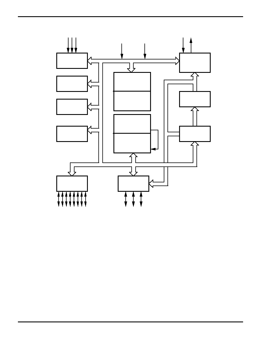
Figure 1. Functional Block Diagram
Port 3
Counter/
Timers (2)
Interrupt
Control
Two Analog
Comparators
Port 2
I/O
(Bit Programmable)
FLAG
Register
Pointer
General-Purpose
Register File
Machine
Timing & Inst.
Control
OTP
Program
Counter
Vcc
GND
XTAL
Port 0
I/O
Input
ALU
Z86E04/E08
CMOS Z8 OTP Microcontrollers
Zilog
4
P R E L I M I N A R Y
DS97Z8X0401
GENERAL DESCRIPTION
(Continued)
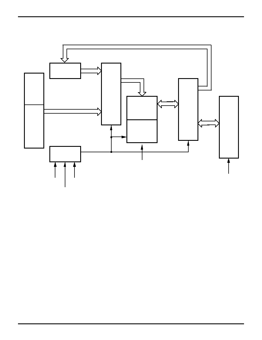
Figure 2. EPROM Programming Mode Block Diagram
Address
MUX
EPROM
ROM PROT
Low Noise
AD 11- 0
Z8 MCU
Z8
Port 0
MSN
Port 3
PGM + Test
Mode Logic
EPM
P32
/CE
XT1
/PGM
P30
D7 - 0
AD 11- 0
AD 11- 0
Data
MUX
Z8
Port 2
D7 - 0
/OE
P31
VPP
P33
D7 - 0
Z86E04/E08
Zilog
CMOS Z8 OTP Microcontrollers
DS97Z8X0401
P R E L I M I N A R Y
5
1
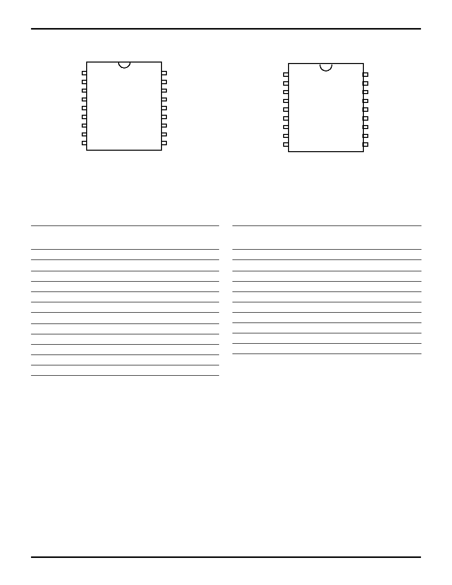
PIN DESCRIPTION
Figure 3. 18-Pin EPROM Mode Configuration
Table 1. 18-Pin DIP Pin Identification
EPROM Programming Mode
Pin #
Symbol
Function
Direction
1≠4
D4≠D7
Data 4, 5, 6, 7
In/Output
5
V
CC
Power Supply
6
N/C
No Connection
7
/CE
Chip Enable
Input
8
/OE
Output Enable
Input
9
EPM
EPROM Prog Mode
Input
10
V
PP
Prog Voltage
Input
11
Clear
Clear Clock
Input
12
Clock
Address
Input
13
/PGM
Prog Mode
Input
14
GND
Ground
15≠18
D0≠D3
Data 0,1, 2, 3
In/Output
D4
D5
D6
D7
VCC
NC
/CE
/OE
EPM
D3
D2
D1
D0
GND
/PGM
CLOCK
CLEAR
VPP
18
1
9
10
Figure 4. 18-Pin DIP/SOIC Mode Configuration
Table 2. 18-Pin DIP/SOIC Pin Identification
Standard Mode
Pin #
Symbol
Function
Direction
1≠4
P24≠P27
Port 2, Pins 4,5,6,7
In/Output
5
V
cc
Power Supply
6
XTAL2
Crystal Osc. Clock
Output
7
XTAL1
Crystal Osc. Clock
Input
8
P31
Port 3, Pin 1, AN1
Input
9
P32
Port 3, Pin 2, AN2
Input
10
P33
Port 3, Pin 3, REF
Input
11≠13
P00≠P02
Port 0, Pins 0,1,2
In/Output
14
GND
Ground
15≠18
P20≠P23
Port 2, Pins 0,1,2,3
In/Output
P24
P25
P26
P27
VCC
XTAL2
XTAL1
P31
P32
P23
P22
P21
P20
GND
P02
P01
P00
P33
18
1
9
10
Z86E04/E08
CMOS Z8 OTP Microcontrollers
Zilog
6
P R E L I M I N A R Y
DS97Z8X0401
ABSOLUTE MAXIMUM RATINGS
Stresses greater than those listed under Absolute Maxi-
mum Ratings may cause permanent damage to the de-
vice. This is a stress rating only; functional operation of the
device at any condition above those indicated in the oper-
ational sections of these specifications is not implied. Ex-
posure to absolute maximum rating conditions for an ex-
tended period may affect device reliability. Total power
dissipation should not exceed 462 mW for the package.
Power dissipation is calculated as follows:
Total Power Dissipation = V
DD
x [I
DD
- (sum of I
OH
)]
+ sum of [(V
DD
- V
OH
) x I
OH
]
+ sum of (V
0L
x I
0L
)
Parameter
Min
Max
Units
Note
Ambient Temperature under Bias
≠40
+105
C
Storage Temperature
≠65
+150
C
Voltage on any Pin with Respect to V
SS
≠0.7
+12
V
1
Voltage on V
DD
Pin with Respect to V
SS
≠0.3
+7
V
Voltage on Pins 7, 8, 9, 10 with Respect to V
SS
≠0.6
V
DD
+1
V
2
Total Power Dissipation
1.65
W
Maximum Allowable Current out of V
SS
300
mA
Maximum Allowable Current into V
DD
220
mA
Maximum Allowable Current into an Input Pin
≠600
+600
µ
A
3
Maximum Allowable Current into an Open-Drain Pin
≠600
+600
µ
A
4
Maximum Allowable Output Current Sinked by Any I/O Pin
25
mA
Maximum Allowable Output Current Sourced by Any I/O Pin
25
mA
Total Maximum Output Current Sinked by a Port
60
mA
Total Maximum Output Current Sourced by a Port
45
mA
Notes:
1. This applies to all pins except where otherwise noted. Maximum current into pin must be
±
600
µ
A.
2. There is no input protection diode from pin to V
DD
(not applicable to EPROM Mode).
3. This excludes Pin 6 and Pin 7.
4. Device pin is not at an output Low state.
Z86E04/E08
Zilog
CMOS Z8 OTP Microcontrollers
DS97Z8X0401
P R E L I M I N A R Y
7
1
STANDARD TEST CONDITIONS
The characteristics listed below apply for standard test
conditions as noted. All voltages are referenced to
Ground. Positive current flows into the referenced pin (Fig-
ure 5).
CAPACITANCE
T
A
= 25
∞
C, V
CC
= GND = 0V, f = 1.0 MHz, unmeasured pins returned to GND.
Figure 5. Test Load Diagram
From Output
Under Test
150 pF
Parameter
Min
Max
Input capacitance
0
10 pF
Output capacitance
0
20 pF
I/O capacitance
0
25 pF
Z86E04/E08
CMOS Z8 OTP Microcontrollers
Zilog
8
P R E L I M I N A R Y
DS97Z8X0401
DC ELECTRICAL CHARACTERISTICS
T
A
= 0
∞
C to +70
∞
C
Typical
Note 4
Sym
Parameter
V
CC
[4]
Min
Max
@ 25
∞
C
Units Conditions
Notes
V
INMAX
Max Input Voltage
3.0V
12
V
I
In
<250
µ
A 1
5.5V
12
V
I
In
<250
µ
A 1
V
CH
Clock Input High
Voltage
3.0V
0.8 V
CC
V
CC
+0.3
1.7
V
Driven by External
Clock Generator
5.5V
0.8 V
CC
V
CC
+0.3
2.8
V
Driven by External
Clock Generator
V
CL
Clock Input Low
Voltage
3.0V
V
SS
≠0.3
0.2 V
CC
0.8
V
Driven by External
Clock Generator
5.5V
V
SS
≠0.3
0.2 V
CC
1.7
V
Driven by External
Clock Generator
V
IH
Input High Voltage
3.0V
5.5V
0.7 V
CC
0.7 V
CC
V
CC
+0.3
V
CC
+0.3
1.8
2.8
V
V
V
IL
Input Low Voltage
3.0V
5.5V
V
SS
≠0.3
V
SS
≠0.3
0.2 V
CC
0.2 V
CC
0.8
1.5
V
V
V
OH
Output High Voltage
3.0V
V
CC
≠0.4
3.0
V
I
OH
= ≠2.0 mA
5
5.5V
V
CC
≠0.4
4.8
V
I
OH
= ≠2.0 mA
5
3.0V
V
CC
≠0.4
3.0
V
Low Noise @ I
OH
= ≠0.5 mA
5.5V
V
CC
≠0.4
4.8
V
Low Noise @ I
OH
= ≠0.5 mA
V
OL1
Output Low Voltage
3.0V
0.8
0.2
V
I
OL
= +4.0 mA
5
5.5V
0.4
0.1
V
I
OL
= +4.0 mA
5
3.0V
0.4
0.2
V
Low Noise @ I
OL
= 1.0 mA
5.5V
0.4
0.1
V
Low Noise @ I
OL
= 1.0 mA
V
OL2
Output Low Voltage
3.0V
1.0
1.0
V
I
OL
= +12 mA,
5
5.5V
0.8
0.8
V
I
OL
= +12 mA,
5
V
OFFSET
Comparator Input
Offset Voltage
3.0V
25.0
10.0
mV
5.5V
25.0
10.0
mV
V
LV
V
CC
Low Voltage
Auto Reset
2.2
3.0
2.8
V
@ 6 MHz Max.
Int. CLK Freq.
I
IL
Input Leakage
(Input Bias
Current of
Comparator)
3.0V
≠1.0
1.0
µ
A
V
IN
= 0V, V
CC
5.5V
≠1.0
1.0
µ
A
V
IN
= 0V, V
CC
I
OL
Output Leakage
3.0V
≠1.0
1.0
µ
A
V
IN
= 0V, V
CC
5.5V
≠1.0
1.0
µ
A
V
IN
= 0V, V
CC
V
ICR
Comparator Input
Common Mode
Voltage Range
0
V
CC
≠1.0
V

Z86E04/E08
Zilog
CMOS Z8 OTP Microcontrollers
DS97Z8X0401
P R E L I M I N A R Y
9
1
T
A
= 0
∞
C to +70
∞
C
Typical
Note 4
Sym
Parameter
V
CC
[4]
Min
Max
@ 25
∞
C
Units Conditions
Notes
I
CC
Supply Current
3.0V
3.5
1.5
mA
All Output and I/O Pins
Floating @ 2 MHz
5,7
5.5V
11.0
6.8
mA
All Output and I/O Pins
Floating @ 2 MHz
5,7
3.0V
8.0
3.0
mA
All Output and I/O Pins
Floating @ 8 MHz
5,7
5.5V
15.0
8.2
mA
All Output and I/O Pins
Floating @ 8 MHz
5,7
3.0V
10.0
3.6
mA
All Output and I/O Pins
Floating @ 12 MHz
5,7
5.5V
20.0
12.0
mA
All Output and I/O Pins
Floating @ 12 MHz
5,7
I
CC1
Standby Current
3.0V
2.5
0.7
mA
HALT Mode V
IN
= 0V,V
CC
@ 2 MHz
5,7
5.5V
4.0
2.5
mA
HALT Mode V
IN
= 0V,V
CC
@ 2 MHz
5,7
3.0V
4.0
1.0
mA
HALT Mode V
IN
= 0V, V
CC
@ 8 MHz
5,7
5.5V
5.0
3.0
mA
HALT Mode V
IN
= 0V, V
CC
@ 8 MHz
5,7
3.0V
4.5
1.5
mA
HALT Mode V
IN
= 0V, V
CC
@ 12 MHz
5,7
5.5V
7.0
4.0
mA
HALT Mode V
IN
= 0V, V
CC
@ 12 MHz
5,7
I
CC
Supply Current
(Low Noise Mode)
3.0V
3.5
1.5
mA
All Output and I/O Pins
Floating @ 1 MHz
7
5.5V
11.0
6.8
mA
All Output and I/O Pins
Floating @ 1 MHz
7
3.0V
5.8
2.5
mA
All Output and I/O Pins
Floating @ 2 MHz
7
5.5V
13.0
7.5
mA
All Output and I/O Pins
Floating @ 2 MHz
7
3.0V
8.0
3.0
mA
All Output and I/O Pins
Floating @ 4 MHz
7
5.5V
15.0
8.2
mA
All Output and I/O Pins
Floating @ 4 MHz
7

Z86E04/E08
CMOS Z8 OTP Microcontrollers
Zilog
10
P R E L I M I N A R Y
DS97Z8X0401
DC ELECTRICAL CHARACTERISTICS (Continued)
T
A
= 0
∞
C to
+70
∞
C
Typical
Note 4
Sym Parameter
V
CC
[4]
Min
Max
@ 25
∞
C
Units
Conditions
Notes
I
CC1
Standby Current
(Low Noise Mode)
3.0V
2.5
0.7
mA
HALT Mode V
IN
= 0V,V
CC
@ 1 MHz
7
5.5V
4.0
2.5
mA
HALT Mode V
IN
= 0V,V
CC
@ 1 MHz
7
3.0V
3.0
0.9
mA
HALT Mode V
IN
= 0V,V
CC
@ 2 MHz
7
5.5V
4.5
2.8
mA
HALT Mode V
IN
= 0V,V
CC
@ 2 MHz
7
3.0V
4.0
1.0
mA
HALT Mode V
IN
= 0V,V
CC
@ 4 MHz
7
5.5V
5.0
3.0
mA
HALT Mode V
IN
= 0V,V
CC
@ 4 MHz
7
I
CC2
Standby Current
3.0V
10.0
1.0
µ
A
STOP Mode V
IN
= 0V, V
CC
WDT is not Running
7,8
5.5V
10.0
1.0
µ
A
STOP Mode V
IN
= 0V,V
CC
WDT is not Running
7,8
I
ALL
Auto Latch Low
Current
3.0V
12.0
3.0
µ
A
0V < V
IN
< V
CC
5.5V
32
16
µ
A
µ
0V < V
IN
< V
CC
I
ALH
Auto Latch High
Current
3.0V
≠8.0
≠1.5
µ
A
µ
0V < V
IN
< V
CC
5.5V
≠16.0
≠8.0
µ
A
0V < V
IN
< V
CC
Notes:
1. Port 2 and Port 0 only
2. V
SS
= 0V = GND
3. The device operates down to V
LV
of the specified frequency for V
LV
.
The minimum operational V
CC
is determined on the value of
the voltage V
LV
at the ambient temperature. The V
LV
increases as the temperature decreases.
4. The V
CC
voltage specification of 3.0 V guarantees 3.3 V
±
0.3 V with typical values measured at V
CC
= 3.3V.
The V
CC
voltage specification of 5.5 V guarantees 5.0 V
±
0.5 V with typical values measured at V
CC
= 5.0 V.
5. Standard Mode (not Low EMI Mode)
6. Z86E08 only
7. All outputs unloaded and all inputs are at V
CC
or V
SS
level.
8. If analog comparator is selected, then the comparator inputs must be at V
CC
level.

Z86E04/E08
Zilog
CMOS Z8 OTP Microcontrollers
DS97Z8X0401
P R E L I M I N A R Y
11
1
T
A
= -40
∞
C to
+105
∞
C
Typical
Note 4
Sym
Parameter
V
CC
[4]
Min
Max
@ 25
∞
C
Units
Conditions
Notes
V
INMAX
Max Input Voltage
4.5V
12.0
V
I
IN
< 250
µ
A
1
5.5V
12.0
V
I
IN
< 250
µ
A
1
V
CH
Clock Input High
Voltage
4.5V
0.8 V
CC
V
CC
+0.3
2.8
V
Driven by External Clock
Generator
5.5V
0.8 V
CC
V
CC
+0.3
2.8
V
Driven by External Clock
Generator
V
CL
Clock Input Low
Voltage
4.5V
V
SS
≠0.3
0.2 V
CC
1.7
V
Driven by External Clock
Generator
5.5V
V
SS
≠0.3
0.2 V
CC
1.7
V
Driven by External Clock
Generator
V
IH
Input High Voltage
4.5V
0.7 V
CC
V
CC
+0.3
2.8
V
5.5V
0.7 V
CC
V
CC
+0.3
2.8
V
V
IL
Input Low Voltage
4.5V
V
SS
≠0.3
0.2 V
CC
1.5
V
5.5V
V
SS
≠0.3
0.2 V
CC
1.5
V
V
OH
Output High Voltage
4.5V
V
CC
≠0.4
4.8
V
I
OH
= ≠2.0 mA
5
5.5V
V
CC
≠0.4
4.8
V
I
OH
= ≠2.0 mA
5
4.5V
V
CC
≠0.4
V
Low Noise @ I
OH
= ≠0.5 mA
5.5V
V
CC
≠0.4
V
Low Noise @ I
OH
= ≠0.5 mA
V
OL1
Output Low Voltage
4.5V
0.4
0.1
V
I
OL
= +4.0 mA
5
5.5V
0.4
0.1
V
I
OL
= +4.0 mA
5
4.5V
0.4
0.1
V
Low Noise @ I
OL
= 1.0 mA
5.5V
0.4
0.1
V
Low Noise @ I
OL
= 1.0 mA
V
OL2
Output Low Voltage
4.5V
1.0
0.3
V
I
OL
= +12 mA,
5
5.5V
1.0
0.3
V
I
OL
= +12 mA,
5
V
OFFSET
Comparator Input
Offset Voltage
4.5V
25.0
10.0
mV
5.5V
25.0
10.0
mV
V
LV
V
CC
Low Voltage
Auto Reset
1.8
3.8
2.8
V
@ 6 MHz Max. Int.
CLK Freq.
3
I
IL
Input Leakage
(Input Bias Current
of Comparator)
4.5V
≠1.0
1.0
µ
A
V
IN
= 0V, V
CC
5.5V
≠1.0
1.0
µ
A
V
IN
= 0V, V
CC
I
OL
Output Leakage
4.5V
≠1.0
1.0
µ
A
V
IN
= 0V, V
CC
5.5V
≠1.0
1.0
µ
A
V
IN
= 0V, V
CC
V
ICR
Comparator Input
Common Mode
Voltage Range
0 V
CC
≠1.5
V

Z86E04/E08
CMOS Z8 OTP Microcontrollers
Zilog
12
P R E L I M I N A R Y
DS97Z8X0401
DC ELECTRICAL CHARACTERISTICS (Continued)
I
CC
Supply Current
4.5V
11.0
6.8
mA
All Output and I/O Pins
Floating @ 2 MHz
5,7
5.5V
11.0
6.8
mA
All Output and I/O Pins
Floating @ 2 MHz
5,7
4.5V
15.0
8.2
mA
All Output and I/O Pins
Floating @ 8 MHz
5,7
5.5V
15.0
8.2
mA
All Output and I/O Pins
Floating @ 8 MHz
5,7
4.5V
20.0
12.0
mA
All Output and I/O Pins
Floating @ 12 MHz
5,7
5.5V
20.0
12.0
mA
All Output and I/O Pins
Floating @ 12 MHz
5,7
I
CC1
Standby Current
4.5V
5.0
2.5
mA
HALT Mode V
IN
= 0V, V
CC
@ 2 MHz
5,7
5.5V
5.0
2.5
mA
HALT Mode V
IN
= 0V, V
CC
@ 2 MHz
5,7
4.5V
5.0
3.0
mA
HALT Mode V
IN
= 0V, V
CC
@ 8 MHz
5,7
5.5V
5.0
3.0
mA
HALT Mode V
IN
= 0V, V
CC
@ 8 MHz
5,7
4.5V
7.0
4.0
mA
HALT Mode V
IN
= 0V, V
CC
@ 12 MHz
5,7
5.5V
7.0
4.0
mA
HALT Mode V
IN
= 0V, V
CC
@ 12 MHz
5,7
I
CC
Supply Current
(Low Noise Mode)
4.5V
11.0
6.8
mA
All Output and I/O Pins
Floating @ 1 MHz
7
5.5V
11.0
6.8
mA
All Output and I/O Pins
Floating @ 1 MHz
7
4.5V
13.0
7.5
mA
All Output and I/O Pins
Floating @ 2 MHz
7
5.5V
13.0
7.5
mA
All Output and I/O Pins
Floating @ 2 MHz
7
4.5V
15.0
8.2
mA
All Output and I/O Pins
Floating @ 4 MHz
7
5.5V
15.0
8.2
mA
All Output and I/O Pins
Floating @ 4 MHz
7
T
A
= -40
∞
C to
+105
∞
C
Typical
Note 4
Sym
Parameter
V
CC
[4]
Min
Max
@ 25
∞
C
Units
Conditions
Notes

Z86E04/E08
Zilog
CMOS Z8 OTP Microcontrollers
DS97Z8X0401
P R E L I M I N A R Y
13
1
T
A
= -40
∞
C to
+105
∞
C
Typical
Note 4
Sym
Parameter
V
CC
[4]
Min
Max
@ 25
∞
C
Units
Conditions
Notes
I
CC1
Standby Current
(Low Noise Mode)
4.5V
4.0
2.5
mA
HALT Mode V
IN
= 0V, V
CC
@ 1 MHz
7
5.5V
4.0
2.5
mA
HALT Mode V
IN
= 0V, V
CC
@ 1 MHz
7
4.5V
4.5
2.8
mA
HALT Mode V
IN
= 0V, V
CC
@ 2 MHz
7
5.5V
4.5
2.8
mA
HALT Mode V
IN
= 0V, V
CC
@ 2 MHz
7
4.5V
5.0
3.0
mA
HALT Mode V
IN
= 0V, V
CC
@ 4 MHz
7
5.5V
5.0
3.0
mA
HALT Mode V
IN
= 0V, V
CC
@ 4 MHz
7
I
CC2
Standby Current
4.5V
20
1.0
µ
A
STOP Mode V
IN
= 0V, V
CC
WDT is not Running
7,8
5.5V
20
1.0
µ
A
STOP Mode V
IN
= 0V, V
CC
WDT is not Running
7,8
I
ALL
Auto Latch Low
Current
4.5V
40
16
µ
A
0V < V
IN
< V
CC
5.5V
40
16
µ
A
0V < V
IN
< V
CC
I
ALH
Auto Latch High
Current
4.5V
≠20.0
≠8.0
µ
A
0V < V
IN
< V
CC
5.5V
≠20.0
≠8.0
µ
A
0V < V
IN
< V
CC
Notes:
1. Port 2 and Port 0 only
2. V
SS
= 0V = GND
3. The device operates down to V
LV
of the specified frequency for V
LV
.
The minimum operational V
CC
is determined on the value of
the voltage V
LV
at the ambient temperature. The V
LV
increases as the temperature decreases.
4. V
CC
= 4.5V to 5.5V, typical values measured at V
CC
= 5.0V
5. Standard Mode (not Low EMI Mode)
6. Z86E08 only
7. All outputs unloaded and all inputs are at V
CC
or V
SS
level.
8. If analog comparator is selected, then the comparator inputs must be at V
CC
level.
Z86E04/E08
CMOS Z8 OTP Microcontrollers
Zilog
14
P R E L I M I N A R Y
DS97Z8X0401
AC ELECTRICAL CHARACTERISTICS
Figure 6. AC Electrical Timing Diagram
1
3
4
8
2
2
3
T
IRQ
IN
N
6
5
7
7
9
Clock
Z86E04/E08
Zilog
CMOS Z8 OTP Microcontrollers
DS97Z8X0401
P R E L I M I N A R Y
15
1
AC ELECTRICAL CHARACTERISTICS
Timing Table (Standard Mode for SCLK/TCLK = XTAL/2)
T
A
= 0
∞
C to +70
∞
C
8 MHz
12 MHz
No
Symbol
Parameter
V
CC
Min
Max
Min
Max
Units
Notes
1
TpC
Input Clock Period
3.0V
125
DC
83
DC
ns
1
5.5V
125
DC
83
DC
ns
1
2
TrC,TfC
Clock Input Rise
and Fall Times
3.0V
25
15
ns
1
5.5V
25
15
ns
1
3
TwC
Input Clock Width
3.0V
62
41
ns
1
5.5V
62
41
ns
1
4
TwTinL
Timer Input Low Width
3.0V
100
100
ns
1
5.5V
70
70
ns
1
5
TwTinH
Timer Input High Width
3.0V
5TpC
5TpC
1
5.5V
5TpC
5TpC
1
6
TpTin
Timer Input Period
3.0V
8TpC
8TpC
1
5.5V
8TpC
8TpC
1
7
TrTin,
TtTin
Timer Input Rise
and Fall Time
3.0V
100
100
ns
1
5.5V
100
100
ns
1
8
TwIL
Int. Request Input
Low Time
3.0V
100
100
ns
1,2
5.5V
70
70
ns
1,2
9
TwIH
Int. Request Input
High Time
3.0V
5TpC
5TpC
1
5.5V
5TpC
5TpC
1,2
10
Twdt
Watch-Dog Timer
Delay Time for Timeout
3.0V
25
25
ms
1
5.5V
12
12
ms
1
11
Tpor
Power-On Reset Time
3.0V
50
180
50
180
ms
1
5.5V
20
80
20
80
ms
1
Notes:
1. Timing Reference uses 0.7 V
CC
for a logic 1 and 0.2 V
CC
for a logic 0.
2. Interrupt request through Port 3 (P33-P31)
3. The V
DD
voltage specification of 3.0V guarantees 3.3V
±
0.3V.
The V
DD
voltage specification of 5.5V guarantees 5.0V
±
0.5V.
Z86E04/E08
CMOS Z8 OTP Microcontrollers
Zilog
16
P R E L I M I N A R Y
DS97Z8X0401
AC ELECTRICAL CHARACTERISTICS
Timing Table (Standard Mode for SCLK/TCLK = XTAL/2)
T
A
= ≠40
∞
C to +105
∞
C
8 MHz
12 MHz
No
Symbol
Parameter
V
CC
Min
Max
Min
Max
Units
Notes
1
TpC
Input Clock Period
4.5V
125
DC
83
DC
ns
1
5.5V
125
DC
83
DC
ns
1
2
TrC,TfC
Clock Input Rise
and Fall Times
4.5V
25
15
ns
1
5.5V
25
15
ns
1
3
TwC
Input Clock Width
4.5V
62
41
ns
1
5.5V
62
41
ns
1
4
TwTinL
Timer Input Low Width
4.5V
70
70
ns
1
5.5V
70
70
ns
1
5
TwTinH
Timer Input High Width
4.5V
5TpC
5TpC
1
5.5V
5TpC
5TpC
1
6
TpTin
Timer Input Period
4.5V
8TpC
8TpC
1
5.5V
8TpC
8TpC
1
7
TrTin,
TtTin
Timer Input Rise
and Fall Time
4.5V
100
100
ns
1
5.5V
100
100
ns
1
8
TwIL
Int. Request Input
Low Time
4.5V
70
70
ns
1,2
5.5V
70
70
ns
1,2
9
TwIH
Int. Request Input
High Time
4.5V
5TpC
5TpC
1
5.5V
5TpC
5TpC
1,2
10
Twdt
Watch-Dog Timer
Delay Time for Timeout
4.5V
10
10
ms
1
5.5V
10
10
ms
1
11
Tpor
Power-On Reset Time
4.5V
12
100
12
100
ms
1
5.5V
12
100
12
100
ms
1
Notes:
1. Timing Reference uses 0.7 V
CC
for a logic 1 and 0.2 V
CC
for a logic 0.
2. Interrupt request made through Port 3 (P33-P31).
Z86E04/E08
Zilog
CMOS Z8 OTP Microcontrollers
DS97Z8X0401
P R E L I M I N A R Y
17
1
AC ELECTRICAL CHARACTERISTICS
Low Noise Mode
T
A
= 0
∞
C to +70
∞
C
1 MHz
4 MHz
No
Symbol
Parameter
V
CC
Min
Max
Min
Max
Units
Notes
1
TPC
Input Clock Period
3.0V
1000
DC
250
DC
ns
1
5.5V
1000
DC
250
DC
ns
1
2
TrC
TfC
Clock Input Rise
and Fall Times
3.0V
25
25
ns
1
5.5V
25
25
ns
1
3
TwC
Input Clock Width
3.0V
500
125
ns
1
5.5V
500
125
ns
1
4.
TwTinL
Timer Input Low Width
3.0V
100
100
ns
1
5.5V
70
70
ns
1
5
TwTinH
Timer Input High Width
3.0V
2.5TpC
2.5TpC
1
5.5V
2.5TpC
2.5TpC
1
6
TpTin
Timer Input Period
3.0V
4TpC
4TpC
1
5.5V
4TpC
4TpC
1
7
TrTin,
TtTin
Timer Input Rise
and Fall Time
3.0V
100
100
ns
1
5.5V
100
100
ns
1
8
TwIL
Low Time
Int. Request Input
3.0V
100
100
ns
1,2
5.5V
70
70
ns
1,2
9
TwIH
High Time
Int. Request Input
3.0V
2.5TpC
2.5TpC
1
5.5V
2.5TpC
2.5TpC
1,2
10
Twdt
Watch-Dog Timer
Delay Time for Timeout
3.0V
25
25
ms
1
5.5V
12
12
ms
1
Notes:
1. Timing Reference uses 0.7 V
CC
for a logic 1 and 0.2 V
CC
for a logic 0.
2. Interrupt request through Port 3 (P33-P31).
3. The V
DD
voltage specification of 3.0V guarantees 3.3V
±
0.3V.
The V
DD
voltage specification of 5.5V guarantees 5.0V
±
0.5V.
Z86E04/E08
CMOS Z8 OTP Microcontrollers
Zilog
18
P R E L I M I N A R Y
DS97Z8X0401
AC ELECTRICAL CHARACTERISTICS (Continued)
Low Noise Mode
T
A
= ≠40
∞
C to +105
∞
C
1 MHz
4 MHz
No
Symbol
Parameter
V
CC
Min
Max
Min
Max
Units
Notes
1
TPC
Input Clock Period
4.5V
1000
DC
250
DC
ns
1
5.5V
1000
DC
250
DC
ns
1
2
TrC
TfC
Clock Input Rise
and Fall Times
4.5V
25
25
ns
1
5.5V
25
25
ns
1
3
TwC
Input Clock Width
4.5V
500
125
ns
1
5.5V
500
125
ns
1
4.
TwTinL
Timer Input Low Width
4.5V
70
70
ns
1
5.5V
70
70
ns
1
5
TwTinH
Timer Input High Width
4.5V
2.5TpC
2.5TpC
1
5.5V
2.5TpC
2.5TpC
1
6
TpTin
Timer Input Period
4.5V
4TpC
4TpC
1
5.5V
4TpC
4TpC
1
7
TrTin,
TtTin
Timer Input Rise
and Fall Time
4.5V
100
100
ns
1
5.5V
100
100
ns
1
8
TwIL
Int. Request Input
Low Time
4.5V
70
70
ns
1,2
5.5V
70
70
ns
1,2
9
TwIH
Int. Request Input
High Time
4.5V
2.5TpC
2.5TpC
1
5.5V
2.5TpC
2.5TpC
1,2
10
Twdt
Watch-Dog Timer
Delay Time for Timeout
4.5V
10
10
ms
1
5.5V
10
10
ms
1
Notes:
1. Timing Reference uses 0.7 V
CC
for a logic 1 and 0.2 V
CC
for a logic 0.
2. Interrupt request through Port 3 (P33-P31).

Z86E04/E08
Zilog
CMOS Z8 OTP Microcontrollers
DS97Z8X0401
P R E L I M I N A R Y
19
1
LOW NOISE VERSION
Low EMI Emission
The Z86E04/E08 can be programmed to operate in a Low
EMI Emission Mode by means of a mask ROM bit option.
Use of this feature results in:
s
All pre-driver slew rates reduced to 10 ns typical.
s
Internal SCLK/TCLK operation limited to a maximum of
4 MHz - 250 ns cycle time.
s
Output drivers have resistances of 500 Ohms (typical).
s
Oscillator divide-by-two circuitry eliminated.
The Low EMI Mode is mask-programmable to be selected
by the customer at the time the ROM code is submitted.
PIN FUNCTIONS
OTP Programming Mode
D7-D0
Data Bus. Data can be read from, or written to, the
EPROM through this data bus.
V
CC
Power Supply. It is typically 5V during EPROM Read
Mode and 6.4V during the other modes (Program, Pro-
gram Verify, and so on).
/CE
Chip Enable (active Low). This pin is active during
EPROM Read Mode, Program Mode, and Program Verify
Mode.
/OE
Output Enable (active Low). This pin drives the Data
Bus direction. When this pin is Low, the Data Bus is output.
When High, the Data Bus is input.
EPM
EPROM Program Mode. This pin controls the differ-
ent EPROM Program Modes by applying different
voltages.
V
PP
Program Voltage. This pin supplies the program volt-
age.
Clear
Clear (active High). This pin resets the internal ad-
dress counter at the High Level.
Clock
Address Clock. This pin is a clock input. The internal
address counter increases by one with one clock cycle.
/PGM
Program Mode (active Low). A Low level at this pin
programs the data to the EPROM through the Data Bus.
Application Precaution
The production test-mode environment may be enabled
accidentally during normal operation if
excessive noise
surges above V
cc
occur on the XTAL1 pin.
In addition, processor operation of Z8 OTP devices may be
affected by
excessive noise surges on the V
pp
, /CE,
/EPM, /OE pins while the microcontroller is in Standard
Mode.
Recommendations for dampening voltage surges in both
test and OTP Mode include the following:
s
Using a clamping diode to V
CC
.
s
Adding a capacitor to the affected pin.
Note: Programming the EPROM/Test Mode Disable
option will prevent accidental entry into EPROM Mode or
Test Mode.
Z86E04/E08
CMOS Z8 OTP Microcontrollers
Zilog
20
P R E L I M I N A R Y
DS97Z8X0401
PIN FUNCTIONS (Continued)
XTAL1, XTAL2
Crystal In, Crystal Out (time-based input
and output, respectively). These pins connect a parallel-
resonant crystal, LC, or an external single-phase clock
(8 MHz or 12 MHz max) to the on-chip clock oscillator and
buffer.
Port 0, P02-P00. Port 0 is a 3-bit bidirectional, Schmitt-trig-
gered CMOS-compatible I/O port. These three I/O lines
can be globally configured under software control to be in-
puts or outputs (Figure 7).
Auto Latch. The Auto Latch puts valid CMOS levels on all
CMOS inputs (except P33, P32, P31) that are not external-
ly driven. A valid CMOS level, rather than a floating node,
reduces excessive supply current flow in the input buffer.
On Power-up and Reset, the Auto Latch will set the ports
to an undetermined state of 0 or 1. Default condition is
Auto Latches enabled.
Figure 7. Port 0 Configuration
Open
Out
In
1.5 2.3 Hysteresis
PAD
Port 0 (I/O)
Z86E04
and
Z86E08
Auto Latch Option
R 500 k
VCC @ 5.0V
Z86E04/E08
Zilog
CMOS Z8 OTP Microcontrollers
DS97Z8X0401
P R E L I M I N A R Y
21
1
Port 2, P27-P20. Port 2 is an 8-bit, bit programmable, bi-
directional, Schmitt-triggered CMOS-compatible I/O port.
These eight I/O lines can be configured under software
control to be inputs or outputs, independently. Bits pro-
grammed as outputs can be globally programmed as ei-
ther push-pull or open-drain (Figure 8).
Figure 8. Port 2 Configuration
Open-Drain
Open
Out
In
1.5 2.3 Hysteresis
PAD
Port 2 (I/O)
Port 2
Z86E04
and
Z86E08
Auto Latch Option
R 500 k
VCC @ 5.0V
Z86E04/E08
CMOS Z8 OTP Microcontrollers
Zilog
22
P R E L I M I N A R Y
DS97Z8X0401
PIN FUNCTIONS (Continued)
Port 3, P33-P31. Port 3 is a 3-bit, CMOS-compatible port
with three fixed input (P33-P31) lines. These three input
lines can be configured under software control as digital
Schmitt-trigger inputs or analog inputs.
These three input lines are also used as the interrupt
sources IRQ0-IRQ3, and as the timer input signal T
IN
(Fig-
ure 9).
Figure 9. Port 3 Configuration
Port 3
Z86E04
and
Z86E08
D1
R247 = P3M
P31 (AN1)
P32 (AN2)
P33 (REF)
cc
DIG.
AN.
+
-
+
-
V
TIN
P31 Data Latch
IRQ2
IRQ3
P32 Data Latch
IRQ0
P33 Data Latch
IRQ1
PAD
PAD
PAD
0 = Digital
1 = Analog
IRQ 0,1,2 = Falling Edge Detection
IRQ3 = Rising Edge Detection
Z86E04/E08
Zilog
CMOS Z8 OTP Microcontrollers
DS97Z8X0401
P R E L I M I N A R Y
23
1
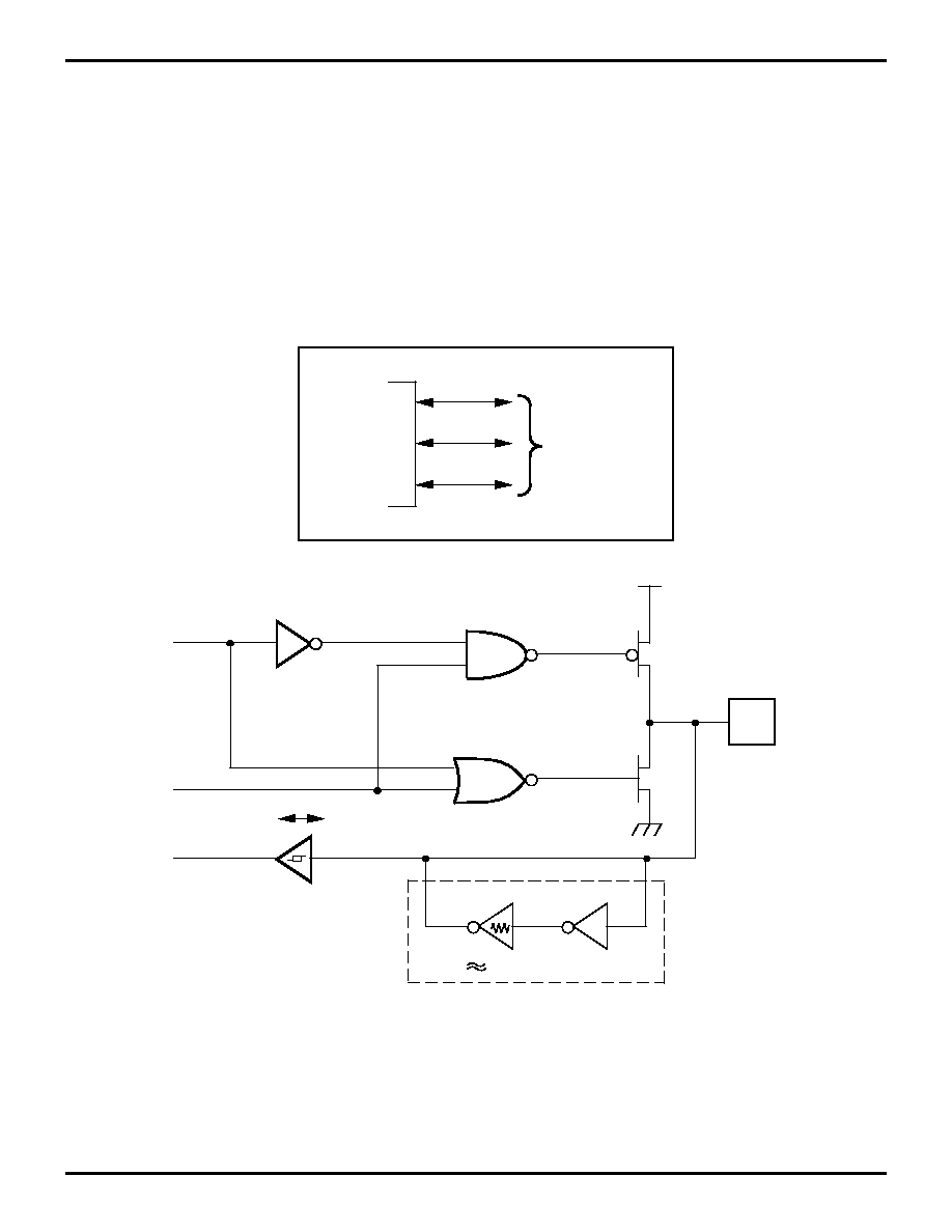
Comparator Inputs. Two analog comparators are added
to input of Port 3, P31, and P32, for interface flexibility. The
comparators reference voltage P33 (REF) is common to
both comparators.
Typical applications for the on-board comparators; Zero
crossing detection, A/D conversion, voltage scaling, and
threshold detection. In Analog Mode, P33 input functions
serve as a reference voltage to the comparators.
The dual comparator (common inverting terminal) features
a single power supply which discontinues power in STOP
Mode. The common voltage range is 0-4 V when the V
CC
is 5.0V; the power supply and common mode rejection ra-
tios are 90 dB and 60 dB, respectively.
Interrupts are generated on either edge of Comparator 2's
output, or on the falling edge of Comparator 1's output.
The comparator output is used for interrupt generation,
Port 3 data inputs, or T
IN
through P31. Alternatively, the
comparators can be disabled, freeing the reference input
(P33) for use as IRQ1 and/or P33 input.
FUNCTIONAL DESCRIPTION
The following special functions have been incorporated
into the Z86E04/E08 devices to enhance the standard Z8
core architecture to provide the user with increased design
flexibility.
RESET. This function is accomplished by means of a Pow-
er-On Reset or a Watch-Dog Timer Reset. Upon power-
up, the Power-On Reset circuit waits for T
POR
ms, plus 18
clock cycles, then starts program execution at address
000C (Hex) (Figure 10). The Z86E04/E08 control registers'
reset value is shown in Table 3.
Power-On Reset (POR)
. A timer circuit clocked by a ded-
icated on-board RC oscillator is used for a POR timer func-
tion. The POR time allows V
CC
and the oscillator circuit to
stabilize before instruction execution begins. The POR
timer circuit is a one-shot timer triggered by one of the four
following conditions:
s
Power-bad to power-good status
s
Stop-Mode Recovery
s
WDT time-out
s
WDH time-out
Watch-Dog Timer Reset. The WDT is a retriggerable
one-shot timer that resets the Z8 if it reaches its terminal
count. The WDT is initially enabled by executing the WDT
instruction and is retriggered on subsequent execution of
the WDT instruction. The timer circuit is driven by an on-
board RC oscillator.
Figure 10. Internal Reset Configuration
INT OSC
XTAL OSC
POR
(Cold Start)
P27
(Stop Mode)
18 CLK
Reset Filiter
Chip Reset
Delay Line
TPOR msec

Z86E04/E08
CMOS Z8 OTP Microcontrollers
Zilog
24
P R E L I M I N A R Y
DS97Z8X0401
FUNCTIONAL DESCRIPTION (Continued)
Table 3. Z86E04/E08 Control Registers
Reset Condition
Addr.
Reg.
D7
D6
D5
D4
D3
D2
D1
D0
Comments
FF
SPL
0
0
0
0
0
0
0
0
FD
RP
0
0
0
0
0
0
0
0
FC
FLAGS
U
U
U
U
U
U
U
U
FB
IMR
0
U
U
U
U
U
U
U
FA
IRQ
U
U
0
0
0
0
0
0
IRQ3 is used for positive edge
detection
F9
IPR
U
U
U
U
U
U
U
U
F8*
P01M
U
U
U
0
U
U
0
1
F7*
P3M
U
U
U
U
U
U
0
0
F6*
P2M
1
1
1
1
1
1
1
1
Inputs after reset
F5
PRE0
U
U
U
U
U
U
U
0
F4
T0
U
U
U
U
U
U
U
U
F3
PRE1
U
U
U
U
U
U
0
0
F2
T1
U
U
U
U
U
U
U
U
F1
TMR
0
0
0
0
0
0
0
0
Note: *Registers are not reset after a STOP-Mode Recovery using P27 pin. A subsequent reset will cause these control registers to
be reconfigured as shown in Table 4 and the user must avoid bus contention on the port pins or it may affect device reliability.
Z86E04/E08
Zilog
CMOS Z8 OTP Microcontrollers
DS97Z8X0401
P R E L I M I N A R Y
25
1
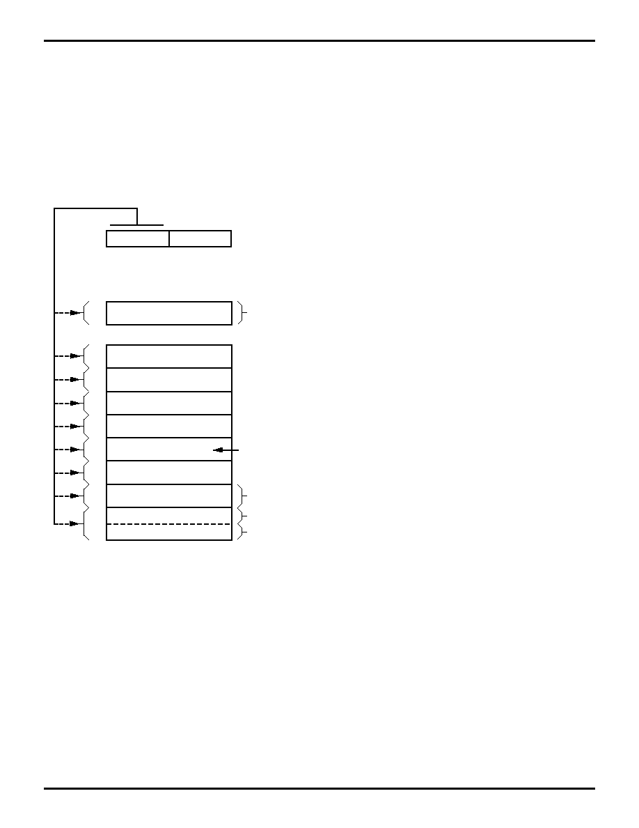
Program Memory. The Z86E04/E08 addresses up to
1K/2KB of Internal Program Memory (Figure 11). The first
12 bytes of program memory are reserved for the interrupt
vectors. These locations contain six 16-bit vectors that cor-
respond to the six available interrupts. Bytes 0-1024/2048
are on-chip one-time programmable ROM.
Register File. The Register File consists of three I/O port
registers, 124 general-purpose registers, and 14 control
and status registers R0-R3, R4-R127 and R241-R255, re-
spectively (Figure 12). General-purpose registers occupy
the 04H to 7FH address space. I/O ports are mapped as
per the existing CMOS Z8.
Figure 11. Program Memory Map
12
11
10
9
8
7
6
5
4
3
2
1
0
On-Chip
ROM
Location of
First Byte of
Instruction
Executed
After RESET
Interrupt
Vector
(Lower Byte)
Interrupt
Vector
(Upper Byte)
IRQ5
IRQ4
IRQ4
IRQ3
IRQ3
IRQ2
IRQ2
IRQ1
IRQ1
IRQ0
IRQ0
IRQ5
1023/2047
0CH
0BH
0AH
09H
08H
07H
06H
05H
04H
03H
02H
01H
00H
3FH/7FFH
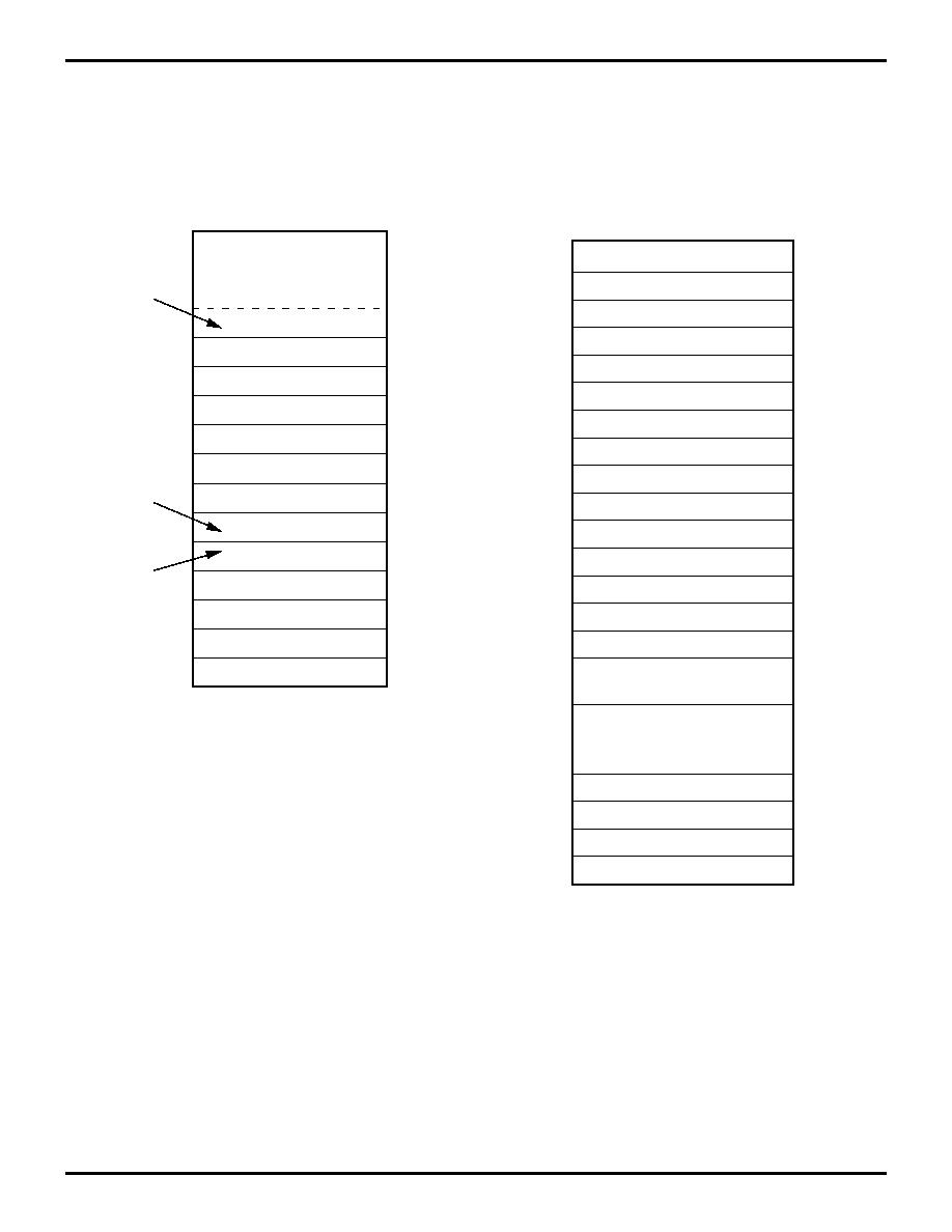
Figure 12. Register File
SPL
Stack Pointer (Bits 7-0)
General-Purpose Register
Register Pointer
Program Control Flags
Interrupt Mask Register
Interrupt Request Register
Interrupt Priority Register
Ports 0-1 Mode
Port 3 Mode
Port 2 Mode
T0 Prescaler
Timer/Counter 0
T1 Prescaler
Timer/Counter 1
Timer Mode
Not Implemented
General-Purpose
Registers
Port 3
Port 2
Reserved
Port 0
RP
IMR
IRQ
IPR
P3M
P2M
PRE0
T0
PRE1
T1
TMR
P3
P2
P1
P0
P01M
FLAGS
Indentifiers
Location
255 (FFH)
254 (FE)
253 (FD)
252 (FC)
251 (FB)
250 (FA)
249 (F9)
248 (F8)
247 (F7)
246 (F6)
245 (F5)
244 (F4)
243 (F3)
242 (F2)
241 (F1H)
4
3
2
1
0 (00H)
128
127 (7FH)
GPR
Z86E04/E08
CMOS Z8 OTP Microcontrollers
Zilog
26
P R E L I M I N A R Y
DS97Z8X0401
FUNCTIONAL DESCRIPTION (Continued)
The Z86E04/E08 instructions can access registers directly
or indirectly through an 8-bit address field. This allows
short 4-bit register addressing using the Register Pointer.
In the 4-bit mode, the register file is divided into eight work-
ing register groups, each occupying 16 continuous loca-
tions. The Register Pointer (Figure 13) addresses the
starting location of the active working-register group.
Stack Pointer. The Z86E04/E08 has an 8-bit Stack Point-
er (R255) used for the internal stack that resides within the
124 general-purpose registers.
General-Purpose Registers (GPR). These registers are
undefined after the device is powered up. The registers
keep their last value after any reset, as long as the reset
occurs in the V
CC
voltage-specified operating range. Note:
Register R254 has been designated as a general-purpose
register and is set to 00 Hex after any reset or Stop-Mode
Recovery.
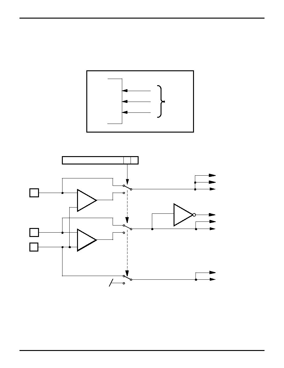
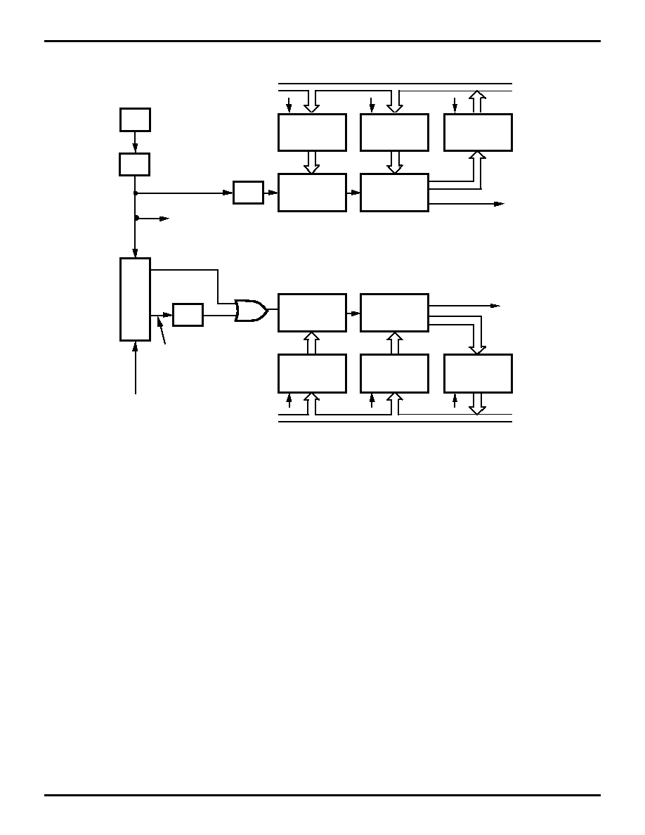
Counter/Timer. There are two 8-bit programmable
counter/timers (T0 and T1), each driven by its own 6-bit
programmable prescaler. The T1 prescaler is driven by in-
ternal or external clock sources; however, the T0 can be
driven by the internal clock source only (Figure 15).
The 6-bit prescalers divide the input frequency of the clock
source by any integer number from 1 to 64. Each prescaler
drives its counter, which decrements the value (1 to 256)
that has been loaded into the counter. When both counter
and prescaler reach the end of count, a timer interrupt re-
quest IRQ4 (T0) or IRQ5 (T1) is generated.
The counter can be programmed to start, stop, restart to
continue, or restart from the initial value. The counters are
also programmed to stop upon reaching zero (Single-Pass
Mode) or to automatically reload the initial value and con-
tinue counting (Modulo-N Continuous Mode).
The counters, but not the prescalers, are read at any time
without disturbing their value or count mode. The clock
source for T1 is user-definable and is either the internal mi-
croprocessor clock divided by four, or an external signal in-
put through Port 3. The Timer Mode register configures the
external timer input (P31) as an external clock, a trigger in-
put that is retriggerable or non-retriggerable, or used as a
gate input for the internal clock.
Figure 13. Register Pointer
The upper nibble of the register file address
provided by the register pointer specifies
the active working-register group.
r7
r6
r5
r4
R253
(Register Pointer)
I/O Ports
Specified Working
Register Group
The lower nibble
of the register
file address
provided by the
instruction points
to the specified
register.
r3
r2
r1
r0
Register Group 1
Register Group 0
R15 to R0
Register Group F
R15 to R4*
R3 to R0
R15 to R0
FF
F0
0F
00
1F
10
2F
20
3F
30
4F
40
5F
50
6F
60
7F
70
*Expanded Register Group (0) is selected in this figure
by handling bits D3 to D0 as "0" in Register R253(RP).
Z86E04/E08
Zilog
CMOS Z8 OTP Microcontrollers
DS97Z8X0401
P R E L I M I N A R Y
27
1
* Note: By passed, if Low EMI Mode is selected.
Figure 14. Counter/Timers Block Diagram
OSC
PRE0
Initial Value
Register
T0
Initial Value
Register
T0
Current Value
Register
6-Bit
Down
Counter
8-bit
Down
Counter
˜
4
6-Bit
Down
Counter
8-Bit
Down
Counter
PRE1
Initial Value
Register
T1
Initial Value
Register
T1
Current Value
Register
˜
2
Clock
Logic
IRQ4
IRQ5
Internal Data Bus
Write
Write
Read
Internal Clock
Gated Clock
Triggered Clock
TIN P31
Write
Write
Read
Internal Data Bus
External Clock
Internal Clock
˜
4
Z86E04/E08
CMOS Z8 OTP Microcontrollers
Zilog
28
P R E L I M I N A R Y
DS97Z8X0401
FUNCTIONAL DESCRIPTION (Continued)
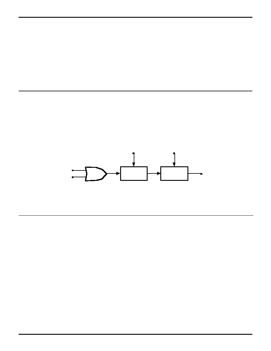
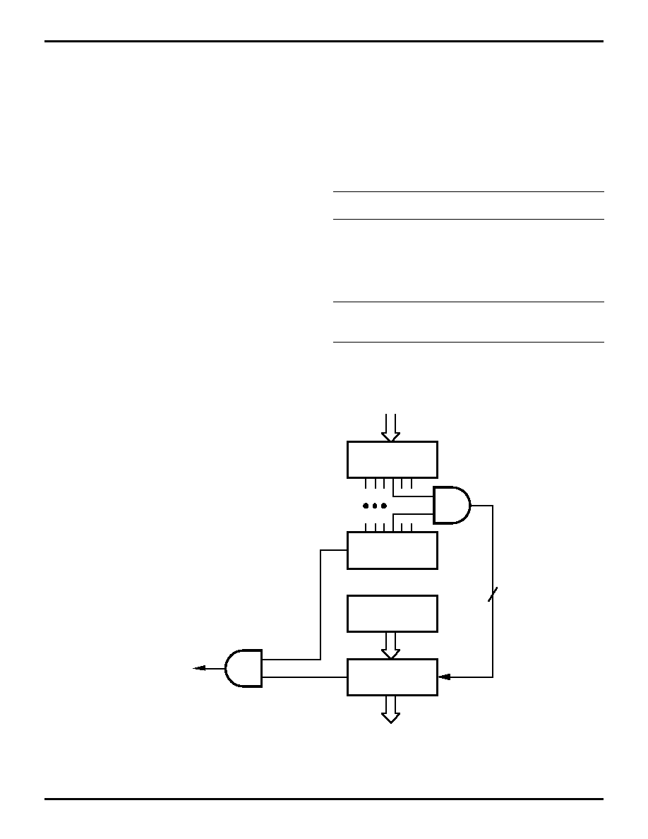
Interrupts. The Z86E04/E08 has six interrupts from six
different sources. These interrupts are maskable and pri-
oritized (Figure 15). The sources are divided as follows:
the falling edge of P31 (AN1), P32 (AN2), P33 (REF), the
rising edge of P32 (AN2), and two counter/timers. The In-
terrupt Mask Register globally or individually enables or
disables the six interrupt requests (Table 4).
When more than one interrupt is pending, priorities are re-
solved by a programmable priority encoder that is con-
trolled by the Interrupt Priority register. All Z86E04/E08 in-
terrupts are vectored through locations in program
memory. When an Interrupt machine cycle is activated, an
Interrupt Request is granted. This disables all subsequent
interrupts, saves the Program Counter and Status Flags,
and then branches to the program memory vector location
reserved for that interrupt. This memory location and the
next byte contain the 16-bit starting address of the interrupt
service routine for that particular interrupt request.
To accommodate polled interrupt systems, interrupt inputs
are masked and the interrupt request register is polled to
determine which of the interrupt requests needs service.
Note: User must select any Z86E08 mode in Zilog's C12
ICEBOX
TM
emulator. The rising edge interrupt is not sup-
ported on the Z86CCP00ZEM emulator.
Table 4. Interrupt Types, Sources, and Vectors
Vector
Name
Source
Location Comments
IRQ0
AN2(P32)
0,1
External (F)Edge
IRQ1
REF(P33)
2,3
External (F)Edge
IRQ2
AN1(P31)
4,5
External (F)Edge
IRQ3
AN2(P32)
6,7
External (R)Edge
IRQ4
T0
8,9
Internal
IRQ5
T1
10,11
Internal
Notes:
F = Falling edge triggered
R = Rising edge triggered
Figure 15. Interrupt Block Diagram
IRQ
IMR
IPR
PRIORITY
LOGIC
6
Global
Interrupt
Enable
Vector Select
Interrupt
Request
IRQ0 - IRQ5
Z86E04/E08
Zilog
CMOS Z8 OTP Microcontrollers
DS97Z8X0401
P R E L I M I N A R Y
29
1
Clock. The Z86E04/E08 on-chip oscillator has a high-
gain, parallel-resonant amplifier for connection to a crystal,
LC, RC, ceramic resonator, or any suitable external clock
source (XTAL1 = INPUT, XTAL2 = OUTPUT). The crystal
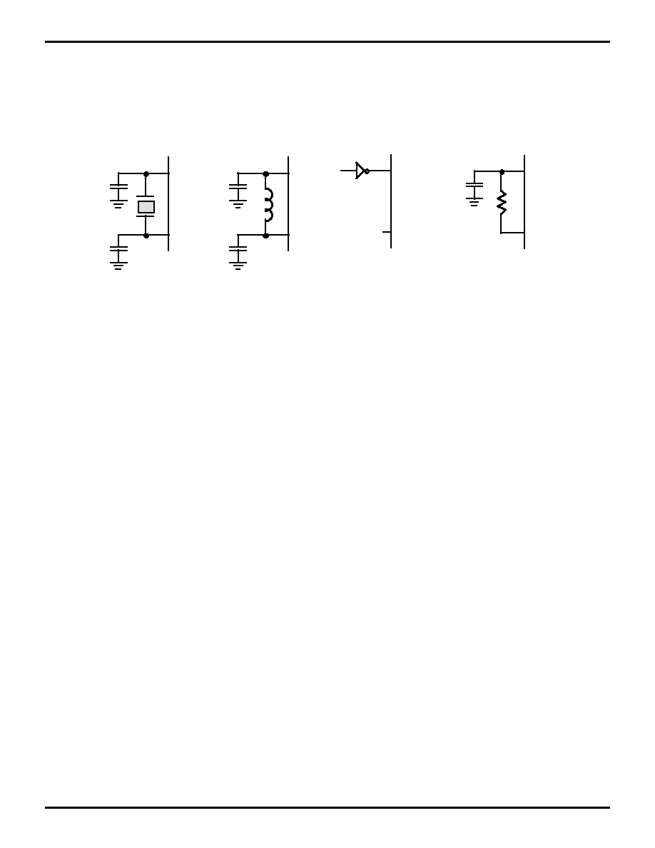
should be AT cut, up to 12 MHz max., with a series resis-
tance (RS) of less than or equal to 100 Ohms.
The crystal should be connected across XTAL1 and
XTAL2 using the vendors crystal recommended capacitors
from each pin directly to device ground pin 14 (Figure 16).
Note that the crystal capacitor loads should be connected
to V
SS
, Pin 14 to reduce Ground noise injection.
Figure 16. Oscillator Configuration
XTAL1
XTAL2
C1
C2
C1
C2
C1
XTAL1
XTAL2
XTAL1
XTAL2
XTAL1
XTAL2
Ceramic Resonator or
Crystal
C1, C2 = 47 pF TYP *
F = 8 MHz
LC
RC
@ 5V Vcc (TYP)
C1 = 100 pF
R = 2K
F = 6 MHz
External Clock
L
R
* Typical value including pin parasitics
*
*
*
*
*
Z86E04/E08
CMOS Z8 OTP Microcontrollers
Zilog
30
P R E L I M I N A R Y
DS97Z8X0401
FUNCTIONAL DESCRIPTION (Continued)
Table 5. Typical Frequency Vs. RC Values
V
CC
= 5.0V @ 25
∞
C
Load Capacitor
Resistor (R)
33 pFd
56 pFd
100 pFd
0.00 1
µ
Fd
A(Hz) B(Hz)
A(Hz)
B(Hz)
A(Hz)
B(Hz)
A(Hz)
B(Hz)
1.0M
33K
31K
20K
20K
12K
11K
1.4K
1.4K
560K
56K
52K
34K
32K
20K
19K
2.5K
2.4K
220K
144K
130K
84K
78K
48K
45K
6K
6K
100K
315K
270K
182K
164K
100K
95K
12K
12K
56K
552K
480K
330K
300K
185K
170K
23K
22K
20K
1.4M
1M
884K
740K
500K
450K
65K
61K
10K
2.6M
2M
1.6M
1.3M
980K
820K
130K
123K
5K
4.4M
3M
2.8M
2M
1.7K
1.3M
245K
225K
2K
8M
5M
6M
4M
3.8K
2.7M
600K
536K
1K
12M
7M
8.8M
6M
6.3K
4.2M
1.0M
950K
Notes:
A = STD Mode Frequency.
B = Low EMI Mode Frequency.
Table 6. Typical Frequency Vs. RC Values
V
CC
= 5.0V @ 25
∞
C
Load Capacitor
Resistor (R)
33 pFd
56 pFd
100 pFd
0.00 1
µ
Fd
A(Hz) B(Hz)
A(Hz)
B(Hz)
A(Hz)
B(Hz)
A(Hz)
B(Hz)
1.0M
18K
18K
12K
12K
7.4K
7.7K
1K
1K
560K
30K
30K
20K
20K
12K
12K
1.6K
1.6K
220K
70K
70K
47K
47K
30K
30K
4K
4K
100K
150K
148K
97K
96K
60K
60K
8K
8K
56K
268K
250K
176K
170K
100K
100K
15K
15K
20K
690M
600K
463K
416K
286K
266K
40K
40K
10K
1.2M
1M
860K
730K
540K
480K
80K
76K
5K
2M
1.7M
1.5M
1.2M
950K
820K
151K
138K
2K
4.6M
3M
3.3M
2.4M
2.2M
1.6M
360K
316K
1K
7M
4.6M
5M
3.6M
3.6K
2.6M
660K
565K
Notes:
A = STD Mode Frequency.
B = Low EMI Mode Frequency.

Z86E04/E08
Zilog
CMOS Z8 OTP Microcontrollers
DS97Z8X0401
P R E L I M I N A R Y
31
1
HALT Mode. This instruction turns off the internal CPU
clock but not the crystal oscillation. The counter/timers and
external interrupts IRQ0, IRQ1, IRQ2 and IRQ3 remain ac-
tive. The device is recovered by interrupts, either external-
ly or internally generated. An interrupt request must be ex-
ecuted (enabled) to exit HALT Mode. After the interrupt
service routine, the program continues from the instruction
after the HALT.
Note: On the C12 ICEBOX, the IRQ3 does not wake the
device out of HALT Mode.
STOP Mode. This instruction turns off the internal clock
and external crystal oscillation and reduces the standby
current to 10
µ
A. The STOP Mode is released by a RESET
through a Stop-Mode Recovery (pin P27). A Low input
condition on P27 releases the STOP Mode. Program exe-
cution begins at location 000C(Hex). However, when P27
is used to release the STOP Mode, the I/O port Mode reg-
isters are not reconfigured to their default power-on condi-
tions. This prevents any I/O, configured as output when the
STOP instruction was executed, from glitching to an un-
known state. To use the P27 release approach with STOP
Mode, use the following instruction:
Note: A low level detected on P27 pin will take the device
out of STOP Mode even if configured as an output.
In order to enter STOP or HALT Mode, it is necessary to
first flush the instruction pipeline to avoid suspending exe-
cution in mid-instruction. To do this, the user executes a
NOP (opcode=FFH) immediately before the appropriate
SLEEP instruction, such as:
Watch-Dog Timer (WDT). The Watch-Dog Timer is en-
abled by instruction WDT. When the WDT is enabled, it
cannot be stopped by the instruction. With the WDT in-
struction, the WDT is refreshed when it is enabled within
every 1 Twdt period; otherwise, the controller resets itself,
The WDT instruction affects the flags accordingly; Z=1,
S=0, V=0.
WDT = 5F (Hex)
Opcode WDT (5FH). The first time Opcode 5FH is execut-
ed, the WDT is enabled and subsequent execution clears
the WDT counter. This must be done at least every T
WDT
;
otherwise, the WDT times out and generates a reset. The
generated reset is the same as a power-on reset of T
POR
,
plus 18 XTAL clock cycles. The software enabled WDT
does not run in STOP Mode.
Opcode WDH (4FH). When this instruction is executed it
enables the WDT during HALT. If not, the WDT stops
when entering HALT. This instruction does not clear the
counters, it just makes it possible to have the WDT running
during HALT Mode. A WDH instruction executed without
executing WDT (5FH) has no effect.
Permanent WDT. Selecting the hardware enabled Perma-
nent WDT option, will automatically enable the WDT upon
exiting reset. The permanent WDT will always run in HALT
Mode and STOP Mode, and it cannot be disabled.
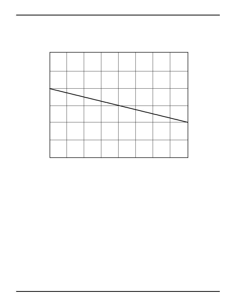
Auto Reset Voltage (V
LV
). The Z86E04/E08 has an auto-
reset built-in. The auto-reset circuit resets the Z86E04/E08
when it detects the V
CC
below V
LV
.
Figure 18 shows the Auto Reset Voltage versus tempera-
ture. If the V
CC
drops below the VCC operating voltage
range, the Z86E04/E08 will function down to the V
LV
un-
less the internal clock frequency is higher than the speci-
fied maximum V
LV
frequency.
LD
P2M, #1XXX XXXXB
NOP
STOP
X = Dependent on user's application.
FF
NOP
; clear the pipeline
6F
STOP
; enter STOP Mode
or
FF
NOP
; clear the pipeline
7F
HALT
; enter HALT Mode
Z86E04/E08
CMOS Z8 OTP Microcontrollers
Zilog
32
P R E L I M I N A R Y
DS97Z8X0401
FUNCTIONAL DESCRIPTION (Continued)
Figure 17. Typical Auto Reset Voltage
(V
LV
) vs. Temperature
2.4
2.5
2.6
2.7
2.8
2.9
Vcc
(Volts)
≠40
∞
C
40
∞
C
Temp
2.3
≠20
∞
C
0
∞
C
20
∞
C
60
∞
C
80
∞
C
100
∞
C

Z86E04/E08
Zilog
CMOS Z8 OTP Microcontrollers
DS97Z8X0401
P R E L I M I N A R Y
33
1
Low EMI Emission
The Z86E04/E08 can be programmed to operate in a low
EMI Emission (Low Noise) Mode by means of an EPROM
programmable bit option. Use of this feature results in:
s
Less than 1 mA consumed during HALT Mode.
s
All drivers slew rates reduced to 10 ns (typical).
s
Internal SCLK/TCLK = XTAL operation limited to a
maximum of 4 MHz - 250 ns cycle time.
s
Output drivers have resistances of 500 ohms (typical).
s
Oscillator divide-by-two circuitry eliminated.
The Z86E04/E08 offers programmable ROM Protect and
programmable Low Noise features. When programmed for
Low Noise, the ROM Protect feature is optional.
In addition to V
DD
and GND (V
SS
), the Z86E04/E08 chang-
es all its pin functions in the EPROM Mode. XTAL2 has no
function, XTAL1 functions as /CE, P31 functions as /OE,
P32 functions as EPM, P33 functions as V
PP
, and P02
functions as /PGM.
ROM Protect. ROM Protect fully protects the Z86E04/E08
ROM code from being read externally. When ROM Protect
is selected, the instructions LDC and LDCI are supported
(Z86E04/E08 and Z86C04/C08 do not support the instruc-
tions of LDE and LDEI). When the device is programmed
for ROM Protect, the Low Noise feature will not automati-
cally be enabled.
Please note that when using the device in a noisy environ-
ment, it is suggested that the voltages on the EPM and CE
pins be clamped to V
CC
through a diode to V
CC
to prevent
accidentally entering the OTP Mode. The V
PP
requires
both a diode and a 100 pF capacitor.
Auto Latch Disable. Auto Latch Disable option bit when
programmed will globally disable all Auto Latches.
WDT Enable. The WDT Enable option bit, when pro-
grammed, will have the hardware enabled Permanent
WDT enabled after exiting reset and can not be stopped in
Halt or Stop Mode.
EPROM/Test Mode Disable. The EPROM/Test Mode
Disable option bit, when programmed, will disable the
EPROM Mode and the Factory Test Mode. Reading, veri-
fying, and programming the Z8 will be disabled. To fully
verify that this mode is disabled, the device must be power
cycled.
User Modes. Table 7 shows the programming voltage of
each mode of Z86E04/E08.
Table 7. OTP Programming Table
Programming Modes
V
PP
EPM
/CE
/OE
/PGM
ADDR
DATA
V
CC
*
EPROM READ1
NU
V
H
V
IL
V
IL
V
IH
ADDR
Out
4.5V
EPROM READ2
NU
V
H
V
IL
V
IL
V
IH
ADDR
Out
5.5V
PROGRAM
V
H
X
V
IL
V
IH
V
IL
ADDR
In
6.4V
PROGRAM VERIFY
V
H
X
V
IL
V
IL
V
IH
ADDR
Out
6.4V
EPROM PROTECT
V
H
V
H
V
H
V
IH
V
IL
NU
NU
6.4V
LOW NOISE SELECT
V
H
V
IH
V
H
V
IH
V
IL
NU
NU
6.4V
AUTO LATCH DISABLE
V
H
V
IH
V
H
V
IL
V
IL
NU
NU
6.4V
WDT ENABLE
V
H
V
IL
V
H
V
IH
V
IL
NU
NU
6.4V
EPROM/TEST MODE
V
H
V
IL
V
H
V
IL
V
IL
NU
NU
6.4V
Notes:
1. V
H
=13.0V
±
0.25 V
DC
.
2. V
IH
= As per specific Z8 DC specification.
3. V
IL
= As per specific Z8 DC specification.
4. X = Not used, but must be set to V
H
or V
IH
level.
5. NU = Not used, but must be set to either V
IH
or V
IL
level.
6. I
PP
during programming = 40 mA maximum.
7. I
CC
during programming, verify, or read = 40 mA maximum.
8. * V
CC
has a tolerance of
±
- 0.25V.
9. V
CC
= 5.0V is acceptable.

Z86E04/E08
CMOS Z8 OTP Microcontrollers
Zilog
34
P R E L I M I N A R Y
DS97Z8X0401
FUNCTIONAL DESCRIPTION (Continued)
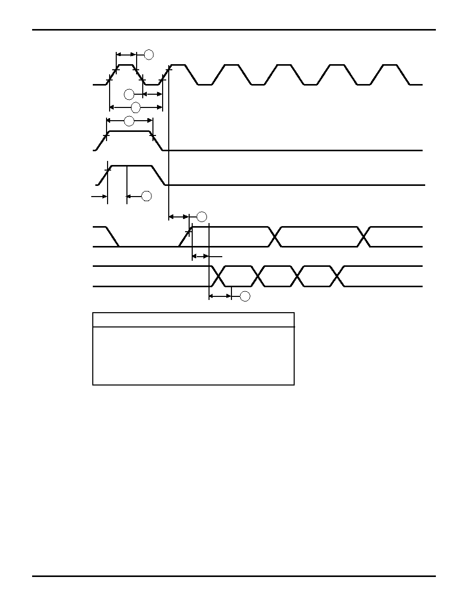
Internal Address Counter. The address of Z86E04/E08
is generated internally with a counter clocked through pin
P01 (Clock). Each clock signal increases the address by
one and the "high" level of pin P00 (Clear) will reset the ad-
dress to zero. Figure 18 shows the setup time of the serial
address input.
Programming Waveform. Figures 19, 20 and 21 show
the programming waveforms of each mode. Table 8 shows
the timing of programming waveforms.
Programming Algorithm. Figure 22 shows the flow chart
of the Z86E04/E08 programming algorithm.
Table 8. Timing of Programming Waveforms
Parameters
Name
Min
Max
Units
1
Address Setup Time
2
µ
s
2
Data Setup Time
2
µ
s
3
V
PP
Setup 2
µ
s
4
V
CC
Setup Time
2
µ
s
5
Chip Enable Setup Time
2
µ
s
6
Program Pulse Width
0.95
ms
7
Data Hold Time
2
µ
s
8
/OE Setup Time
2
µ
s
9
Data Access Time
188
ns
10
Data Output Float Time
100
ns
11
Overprogram Pulse Width
2.85
ms
12
EPM Setup Time
2
µ
s
13
/PGM Setup Time
2
µ
s
14
Address to /OE Setup Time
2
µ
s
15
Option Program Pulse Width
78
ms
16
/OE Width
250
ns
17
Address Valid to /OE Low
125
ns
Z86E04/E08
Zilog
CMOS Z8 OTP Microcontrollers
DS97Z8X0401
P R E L I M I N A R Y
35
1
Figure 18. Z86E04/E08 Address Counter Waveform
P01 = Clock
P00 = Clear
T2
T4
T3
T1
Internal
Address
T5
0 Min
9
Data
Vih
Vil
Invalid
Valid
Invalid
Valid
Legend:
T1 Reset Clock Width
T2 Input Clock High
T3 Input Clock Period
T4 Input Clock Low
T5 Clock to Address Counter Out Delay
T6 Epm/Vpp Set up Time
30 ns Min
100 ns Min
200 ns Min
100 ns Min
15 ns Max
40
µ
s Min
T6
Vpp/EPM
Z86E04/E08
CMOS Z8 OTP Microcontrollers
Zilog
36
P R E L I M I N A R Y
DS97Z8X0401
FUNCTIONAL DESCRIPTION (Continued)
Figure 19. Z86E04/E08 Programming Waveform
(EPROM Read)
Data
VIH
VIL
Invalid
Valid
Invalid
Valid
VIH
VIL
Address Stable
Address
Address Stable
17
9
12
5
EPM
VH
VIL
VCC
4.5V
/CE
VIH
VIL
/OE
VIH
VIL
VPP
VH
VIL
5.5V
/PGM
VIH
VIL
3
16
16
17
16
Z86E04/E08
Zilog
CMOS Z8 OTP Microcontrollers
DS97Z8X0401
P R E L I M I N A R Y
37
1
Figure 20. Z86E04/E08 Programming Waveform
(Program and Verify)
Address
V
IH
V
IL
Address Stable
Data
V
IH
V
IL
Data Stable
Data Out Valid
1
2
10
9
3
V
PP
V
H
V
IH
EPM
V
IL
4
7
/CE
V
IL
6
8
11
/PGM
V
IH
V
IL
V
IH
V
H
VCC
4.5V
6V
/OE
V
IH
V
IL
Program Cycle
Verify Cycle
16
13
5
Z86E04/E08
CMOS Z8 OTP Microcontrollers
Zilog
38
P R E L I M I N A R Y
DS97Z8X0401
FUNCTIONAL DESCRIPTION (Continued)
Figure 21. Z86E04/E08 Programming Options Waveform
(EPROM Protect and Low Noise Program)
Address
V
IH
V
IL
Data
V
IH
V
IL
V
PP
V
IH
V
CC
6V
/OE
3
4
5
/CE
V
H
V
IH
/PGM
V
IH
V
IL
12
15
15
EPM
V
H
V
IL
EPROM
Protect
Low
Noise
4.5V
V
IH
V
IH
V
IH
V
H
12
13
13
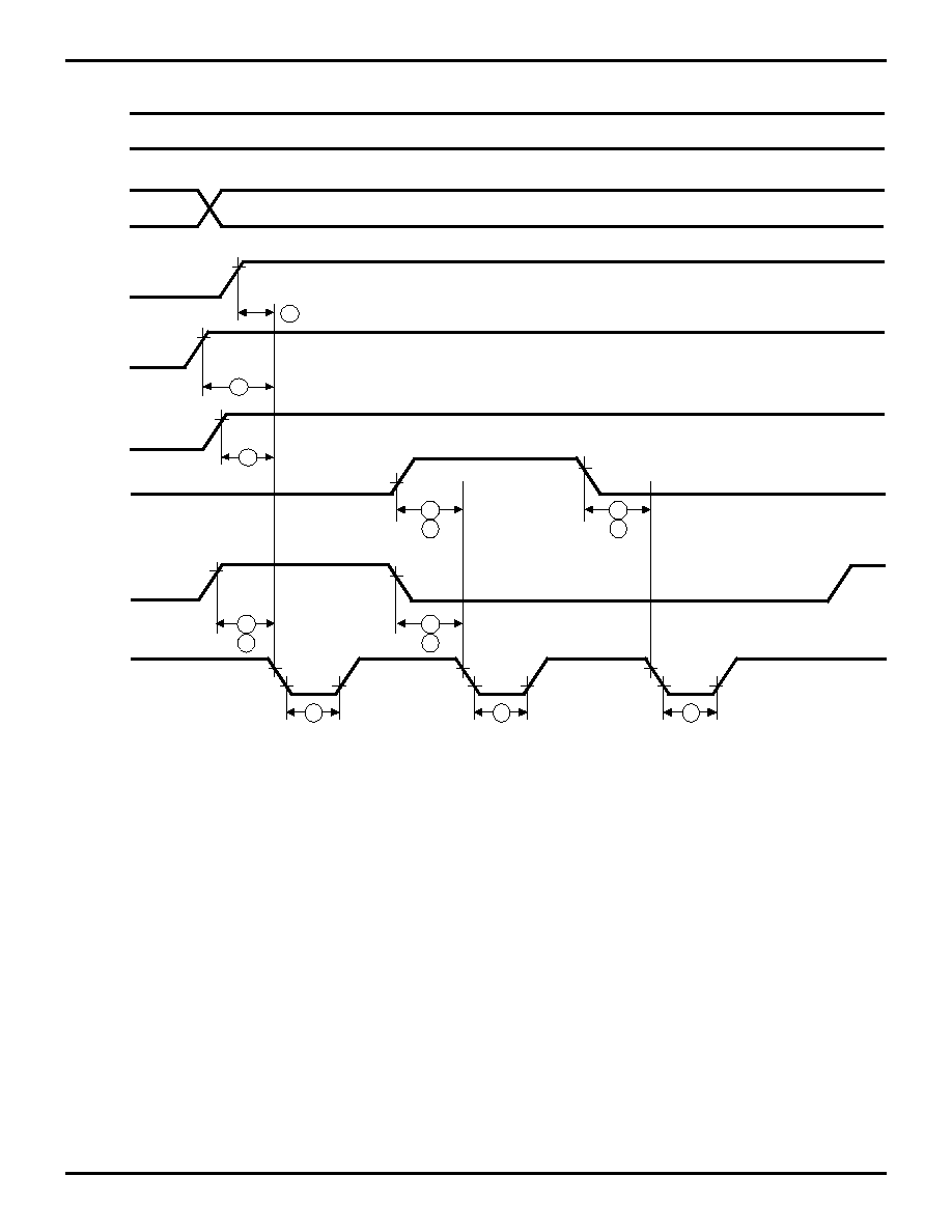
Z86E04/E08
Zilog
CMOS Z8 OTP Microcontrollers
DS97Z8X0401
P R E L I M I N A R Y
39
1
Figure 22. Z86E04/E08 Programming Options Waveform
(Auto Latch Disable, Permanent WDT Enable and
EPROM/Test Mode Disable)
Address
V
IH
V
IL
Data
V
IH
V
IL
V
PP
V
IH
V
CC
6V
/OE
3
4
5
/CE
V
H
V
IH
/PGM
V
IH
V
IL
12
15
15
EPM
V
IH
Auto Latch
WDT
4.5V
V
IL
V
IL
V
IH
V
H
12
12
12
15
EPROM/Test
Mode Disable
13
13
13
13
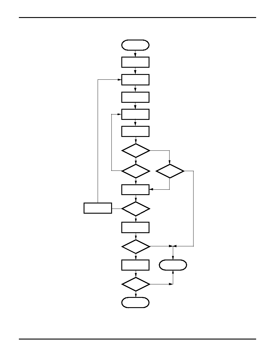
Z86E04/E08
CMOS Z8 OTP Microcontrollers
Zilog
40
P R E L I M I N A R Y
DS97Z8X0401
FUNCTIONAL DESCRIPTION (Continued)
Figure 23. Z86E04/E08 Programming Algorithm
Start
Vcc = 6.4V
Vpp = 13.0V
N = 0
Program
1 ms Pulse
Increment N
N = 25 ?
Yes
No
Verify
One Byte
Pass
Fail
Prog. One Pulse
3xN ms Duration
Verify Byte
Fail
Pass
Increment
Address
Last Addr ?
Yes
No
Vcc = Vpp = 4.5V
Verify All
Bytes
Device Failed
Addr =
First Location
Fail
Pass
Vcc = Vpp = 5.5V
Verify All
Bytes
Device Passed
Pass
Fail
Z86E04/E08
Zilog
CMOS Z8 OTP Microcontrollers
DS97Z8X0401
P R E L I M I N A R Y
41
1
Z8 CONTROL REGISTERS
Figure 24. Timer Mode Register (F1
H
: Read/Write)
Figure 25. Counter Timer 1 Register (F2
H
: Read/Write)
Figure 26. Prescaler 1 Register (F3
H
: Write Only)
D7
D6
D5
D4
D3
D2
D1
D0
0 Disable T0 Count
1 Enable T0 Count
0 No Function
1 Load T0
0 No Function
1 Load T1
0 Disable T1 Count
1 Enable T1 Count
TIN Modes
00 External Clock Input
01 Gate Input
10 Trigger Input
(Non-retriggerable)
11 Trigger Input
(Retriggerable)
Reserved (Must be 0)
R241 TMR
D7
D6
D5
D4 D3
D2
D1
D0
T Initial Value
(When Written)
(Range 1-256 Decimal
01-00 HEX)
T Current Value
(When READ)
1
1
R242 T1
D7
D6
D5
D4
D3 D2
D1
D0
Count Mode
0 = T Single Pass
1 = T Modulo N
1
1
Clock Source
1 = T Internal
0 = T External Timing Input
(T ) Mode
IN
1
1
Prescaler Modulo
(Range: 1-64 Decimal
01-00 HEX)
R243 PRE1
Figure 27. Counter/Timer 0 Register
(F4
H
: Read/Write)
Figure 28. Prescaler 0 Register (F5
H
: Write Only)
Figure 29. Port 2 Mode Register (F6
H
: Write Only)
Figure 30. Port 3 Mode Register (F7
H
: Write Only)
D7
D6
D5
D4
D3
D2
D1
D0
T Initial Value
(When Written)
(Range: 1-256 Decimal
01-00 HEX)
T Current Value
(When READ)
0
0
R244 T0
D7
D6
D5
D4
D3
D2
D1
D0
Count Mode
0 T0 Single Pass
1 T0 Modulo N
Reserved (Must be 0)
R245 PRE0
Prescaler Modulo
(Range: 1-64 Decimal
01-00 HEX)
D7 D6
D5
D4 D3
D2 D1
D0
P2 - P2 I/O Definition
0 Defines Bit as OUTPUT
1 Defines Bit as INPUT
7
0
R246 P2M
D7
D6
D5
D4
D3
D2
D1
D0
R247 P3M
0 Port 2 Open-Drain
1 Port 2 Push-pull
Reserved (Must be 0)
Port 3 Inputs
0 Digital Mode
1 Analog Mode
Z86E04/E08
CMOS Z8 OTP Microcontrollers
Zilog
42
P R E L I M I N A R Y
DS97Z8X0401
Z8 CONTROL REGISTERS (Continued)
Figure 31. Port 0 and 1 Mode Register
(F8
H
: Write Only)
Figure 32. Interrupt Priority Register
(F9
H
: Write Only)
Figure 33. Interrupt Request Register
(FA
H
: Read/Write)
D7
D6
D5
D4
D3
D2
D1
D0
P0
2
-P0
0
Mode
00 = Output
01 = Input
Reserved (Must be 1.)
R248 P01M
Reserved (Must be 0.)
D7
D6 D5 D4
D3 D2 D1
D0
Interrupt Group Priority
Reserved = 000
C > A > B = 001
A > B > C = 010
A > C > B = 011
B > C > A = 100
C > B > A = 101
B > A > C = 110
Reserved = 111
IRQ3, IRQ5 Priority (Group A)
0 = IRQ5 > IRQ3
1 = IRQ3 > IRQ5
IRQ0, IRQ2 Priority (Group B)
0 = IRQ2 > IRQ0
1 = IRQ0 > IRQ2
IRQ1, IRQ4 Priority (Group C)
0 = IRQ1 > IRQ4
1 = IRQ4 > IRQ1
Reserved (Must be 0.)
R249 IPR
D7 D6
D5
D4
D3 D2
D1
D0
R250 IRQ
Reserved (Must be 0)
IRQ0 = P32 Input
IRQ1 = P33 Input
IRQ2 = P31 Input
IRQ3 = P32 Input
IRQ4 = T0
IRQ5 = T1
Figure 34. Interrupt Mask Register
(FB
H
: Read/Write)
Figure 35. Flag Register
(FC
H
: Read/Write)
Figure 36. Register Pointer
(FD
H
: Read/Write)
Figure 37. Stack Pointer
(FF
H
: Read/Write)
D7
D6
D5
D4 D3
D2
D1
D0
Reserved (Must be 0.)
1 Enables IRQ0-IRQ5
(D = IRQ0)
1 Enables Interrupts
0
R251 IMR
D7
D6
D5
D4
D3
D2
D1
D0
User Flag F1
User Flag F2
Half Carry Flag
Decimal Adjust Flag
Overflow Flag
Sign Flag
Zero Flag
Carry Flag
R252 Flags
D7
D6
D5
D4
D3
D2
D1
D0
R253 RP
Expanded Register File
Working Register Pointer
Default After Reset = 00H
D7 D6
D5 D4 D3
D2 D1 D0
Stack Pointer Lower
Byte (SP - SP )
0
7
R255 SPL
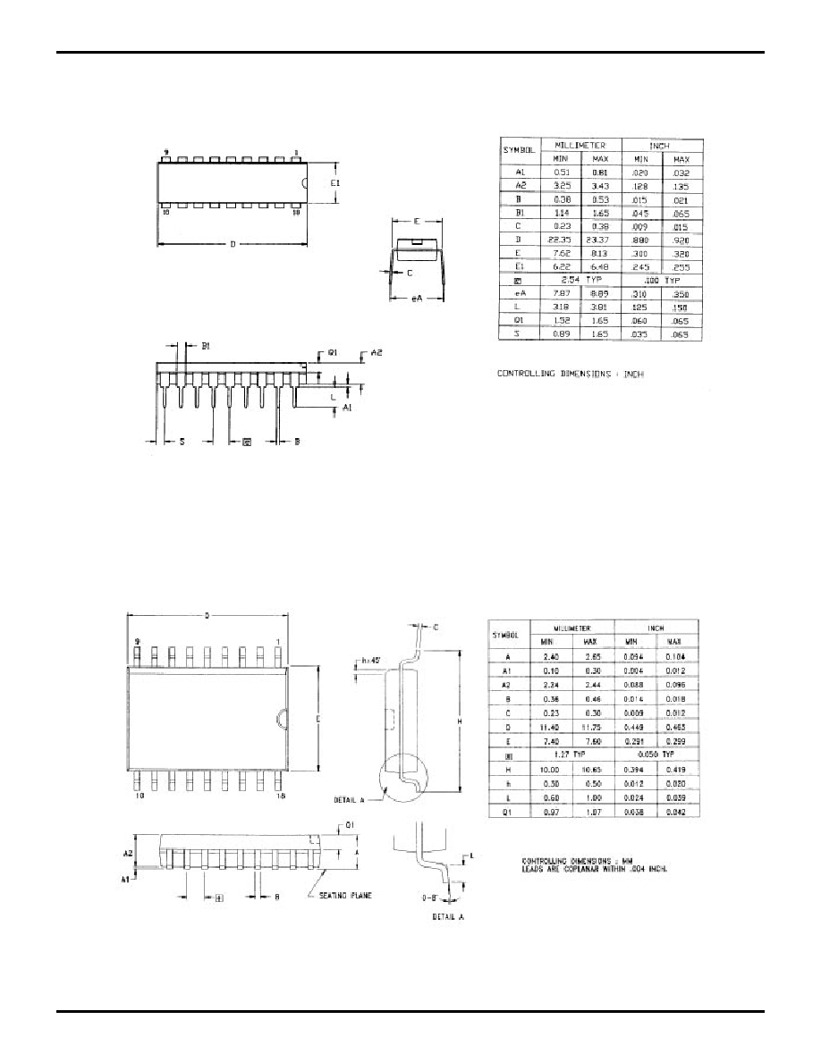
Z86E04/E08
Zilog
CMOS Z8 OTP Microcontrollers
DS97Z8X0401
P R E L I M I N A R Y
43
1
PACKAGE INFORMATION
18-Pin DIP Package Diagram
18-Pin SOIC Package Diagram

Z86E04/E08
CMOS Z8 OTP Microcontrollers
Zilog
44
P R E L I M I N A R Y
DS97Z8X0401
ORDERING INFORMATION
Z86E04
Z86E08
For fast results, contact your local Zilog sales office for assistance in ordering the part(s) desired.
Codes
Preferred Package
P = Plastic DIP
Longer Lead Time
S = SOIC
Preferred Temperature
S = 0
∞
C to +70
∞
C
E = ≠40
∞
C to +105
∞
C
Speeds
12 =12 MHz
Environmental
C = Plastic Standard
© 1997 by Zilog, Inc. All rights reserved. No part of this
document may be copied or reproduced in any form or by
any means without the prior written consent of Zilog, Inc.
The information in this document is subject to change
without notice. Devices sold by Zilog, Inc. are covered by
warranty and patent indemnification provisions appearing
in Zilog, Inc. Terms and Conditions of Sale only. Zilog, Inc.
makes no warranty, express, statutory, implied or by
description, regarding the information set forth herein or
regarding the freedom of the described devices from
intellectual property infringement. Zilog, Inc. makes no
warranty of merchantability or fitness for any purpose.
Zilog, Inc. shall not be responsible for any errors that may
appear in this document. Zilog, Inc. makes no commitment
to update or keep current the information contained in this
document.
Zilog's products are not authorized for use as critical
components in life support devices or systems unless a
specific written agreement pertaining to such intended use
is executed between the customer and Zilog prior to use.
Life support devices or systems are those which are
intended for surgical implantation into the body, or which
sustains life whose failure to perform, when properly used
in accordance with instructions for use provided in the
labeling, can be reasonably expected to result in
significant injury to the user.
Zilog, Inc. 210 East Hacienda Ave.
Campbell, CA 95008-6600
Telephone (408) 370-8000
FAX (408) 370-8056
Internet: www.zilog.com
Standard and Extended Temperature
18-Pin DIP
18-Pin SOIC
Z86E0412PSC
Z86E04012SC
Z86E0412PEC
Z86E0412SEC
Standard and Extended Temperature
18-Pin DIP
18-Pin SOIC
Z86E0812PSC
Z86E0812SSC
Z86E0812PEC
Z86E0812SEC
Example:
Z 86E04 12 P S C
Environmental Flow
Temperature
Package
Speed
Product Number
Zilog Prefix
is a Z86E04, 12 MHz, DIP, 0
∞
C to +70
∞
C, Plastic Standard Flow