1
Z86E03/E06
CP95DZ81301
P R E L I M I N A R Y
CP95DZ81301 (8/95)
P
RELIMINARY
C
USTOMER
P
ROCUREMENT
S
PECIFICATION
FEATURES
GENERAL DESCRIPTION
The Z86E03/E06 are One-Time Programmable (OTP)
members of the Z8
Æ
microcontroller family allowing easy
software development, debug, and prototyping for small
production runs that are not economically desirable with a
masked ROM version.
Three address spaces, the Program Memory, Register
File, and Expanded Register File (ERF), support a wide
range of memory configurations. Through the ERF, the
designer has access to four additional control registers
that provide extra peripheral devices, I/O ports, register
addresses, an SPI receive buffer and SPI compare
register.
ROM
RAM*
Speed
Part
(Kbytes)
(Kbytes)
SPI
(MHz)
Z86E03
512
61
No
8
Z86E06
1
125
Yes
12
Z86E03/E06
CMOS Z8
Æ
OTP
M
ICROCONTROLLERS
For applications demanding powerful I/O capabilities, the
Z86E03/E06's dedicated input and output lines are grouped
into two ports, and are configurable under software control
to provide timing, status signals, or parallel I/O.
Notes:
All Signals with a preceding front slash, "/", are active Low, e.g.:
B//W (WORD is active Low); /B/W (BYTE is active Low, only).
Power connections follow conventional descriptions below:
Connection
Circuit
Device
Power
V
CC
V
DD
Ground
GND
V
SS
*General-Purpose
s
18-Pin DIP, WIN, and SOIC Packages
s
4.5- to 5.5-Volt Operating Range
s
0
∞
C to +70
∞
C Temperature Range
s
Low-Power Consumption
s
Expanded Register File (ERF)
s
14 Input/Output Lines
s
Serial Peripheral Interface (SPI) (Z86E06 Only)
s
Software Watch-Dog Timer (WDT)
s
Power-On Reset (POR)

2
Z86E03/E06
CP95DZ81301
P R E L I M I N A R Y
GENERAL DESCRIPTION
(Continued)
Port 3
Counter/
Timer
Interrupt
Control
Two Analog
Comparators
Port 2
I/O
(Bit Programmable)
ALU
FLAG
Register
Pointer
Register File
142 x 8-Bit*
Vcc
GND
XTAL
Input
Output
Machine
Timing & Inst.
Control
Prg. Memory
1K x 8-Bit*
Program
Counter
WDT, POR
Note:
*The Z86E03 has 512 x 8-Bit Program
Memory and 78 x 8-Bit Register File.
Functional Block Diagram
3
Z86E03/E06
CP95DZ81301
P R E L I M I N A R Y
GENERAL DESCRIPTION
(Continued)
1
2
9
3
4
5
6
7
8
18
17
16
15
14
13
12
11
10
D3
D2
VPP
D1
D0
GND
/PGM
CLOCK
CLEAR
D4
D5
EPM
D6
D7
Vcc
N/C
/CE
/OE
Z86E03/E06
EPROM
1
2
9
3
4
5
6
7
8
18
17
16
15
14
13
12
11
10
P23
P22
P33
P21
P20
GND
P36
P35
P34
P24
P25
P32
P26
P27
Vcc
XTAL2
XTAL1
P31
Z86E03/
E06
PDIP
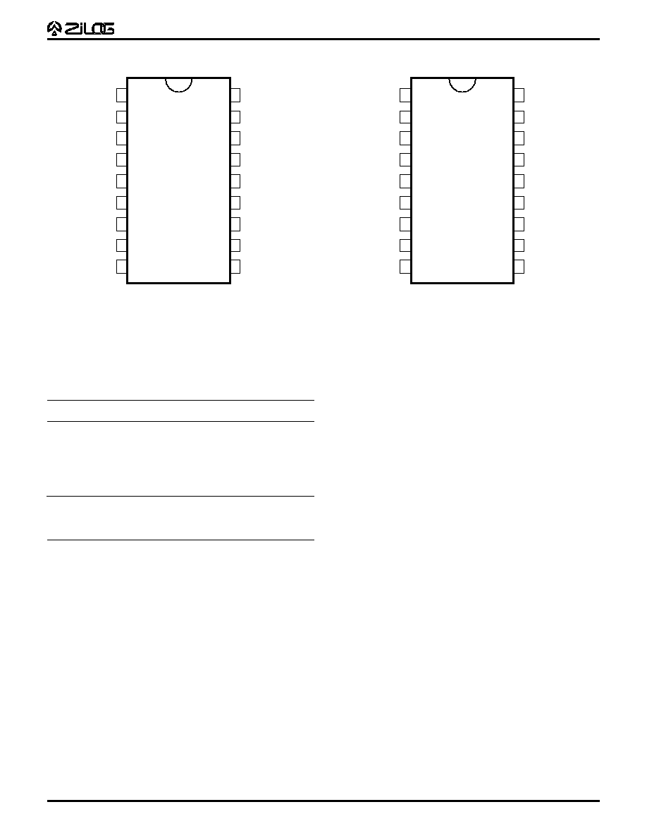
18-Pin DIP/WIN
Pin Configuration
18-Pin EPROM Mode
Pin Configuration
18-Pin Identification
Pin #
Symbol Function
Direction
1-4
P24-P27 Port 2, Pins 4,5,6,7
Input/Output
5
V
CC
Power Supply
6
XTAL2
Crystal Oscillator Clock Output
7
XTAL1
Crystal Oscillator Clock Input
8-10
P31-P33 Port 3, Pins 1,2,3
Fixed Input
11-13
P34-P36 Port 3, Pins 4,5,6
Fixed Output
14
GND
Ground
15-18
P20-23
Port 2, Pins 0,1,2,3
Input/Output

4
Z86E03/E06
CP95DZ81301
P R E L I M I N A R Y
ABSOLUTE MAXIMUM RATINGS
Symbol
Description
Min
Max
Units
V
CC
Supply Voltage*
≠0.3
+7.0
V
V
IN
Input Voltage**
≠0.3
V
CC
+ 0.3
V
T
STG
Storage Temp
≠65
+150
C
T
A
Oper Ambient Temp
C
Stress greater than those listed under Absolute Maximum
Ratings may cause permanent damage to the device. This
is a stress rating only; operation of the device at any
condition above those indicated in the operational sec-
tions of these specifications is not implied. Exposure to
absolute maximum rating conditions for extended period
may affect device reliability.
Notes:
* Voltage on Vcc with respect to Vss.
See Ordering Information
** Voltages on all pins with respect to Vss without current limitations.
STANDARD TEST CONDITIONS
The characteristics listed below apply for standard test
conditions as noted. All voltages are referenced to ground.
Positive current flows into the referenced pin (Test Load
Configuration).
Test Load Configuration
GENERAL DESCRIPTION
(Continued)
18-Pin SOIC
Pin Configuration
150 pF
1
18
P24
P27
Vcc
XTAL2
XTAL1
P31
P32
P23
P22
P21
P20
GND
P36
P35
P34
P33
Z86E03/E06
SOIC
P25
P26
2
3
4
5
6
7
8
9
17
16
15
14
13
12
10
11

5
Z86E03/E06
CP95DZ81301
P R E L I M I N A R Y
DC ELECTRICAL CHARACTERISTICS
T
A
= 0
∞
C to 70
∞
C
V
CC
(4.5V to 5.5V) Typical
Symbol Parameter
Note [3] Min
Max
@ 25
∞
C
Units
Conditions Notes
Max Input Voltage
5.0V
12
V
I
IN
250
µ
A
[8]
V
CH
Clock Input High
5.0V
0.9 V
CC
V
CC
+0.3
2.7
V
Driven by External
Voltage
Clock Generator
V
CL
Clock Input Low
5.0V
V
SS
≠0.3
0.2 V
CC
1.7
V
Driven by External
Voltage
Clock Generator
V
IH
Input High Voltage
5.0V
0.7 V
CC
V
CC
+0.3
2.5
V
V
IL
Input Low Voltage
5.0V
V
SS
≠0.3
0.2 V
CC
1.6
V
V
OH
Output High Voltage 5.0V
V
CC
≠0.4
4.9
V
I
OH
= ≠2.0 mA
[10]
(Low EMI Mode)
5.0V
V
CC
≠0.4
4.9
V
I
OH
= ≠0.5 mA
V
OL1
Output Low Voltage 5.0V
0.4
0.1
V
I
OL
=+4.0 mA
[10]
(Low EMI Mode)
5.0V
0.4
0.1
V
I
OL
=+1.0 mA
V
OL2
Output Low Voltage 5.0V
1.0
0.3
V
I
OL
= +12 mA,
[10]
V
OFFSET
Comparator Input
5.0V
±
10
±
5
mV
V
ICR
Input Common
5.0V
OV
V
CC
≠1.5v
[7]
Mode Voltage Range
I
IL
Input Leakage
5.0V
≠1.0
1.0
µ
A
V
IN
= OV, V
CC
I
OL
Output Leakage
5.0V
≠1.0
1.0
µ
A
V
IN
= OV, V
CC
I
CC
Supply Current
5.0V
11.0
8.0
mA
@ 8 MHz
[4, 5, 12]
5.0V
15
11
mA
@ 12 MHz
[4, 5, 13]
I
OB
Input Bias Current
5.0V
300
nA
[7]
I
IO
Input Offset Current 5.0V
±
150
nA
[7]
6
Z86E03/E06
CP95DZ81301
P R E L I M I N A R Y
Notes:
[1]
I
CC1
Typ
Max
Unit
Freq
Clock Driven
3.0
5.0
mA
8 MHz
Crystal or Ceramic Resonator
0.3
5.0
mA
8 MHz
[2] V
SS
= 0V = GND
[3] The V
POR
increases as the temperature decreases.
[4] All outputs unloaded, I/O pins floating, inputs at rail.
[5] C
L1
= C
L2
= 100 pF
[6] Same as note [4] except inputs at V
CC
.
[7] For analog comparator inputs when analog comparators are
enabled.
[8] Excludes clock pins and Port 3 inputs.
[9] Clock must be forced low when XTAL1 is clock driven and XTAL2 is
floating.
[10] Standard mode (not low EMI mode).
[11] Low EMI oscillator enabled.
[12] Z86E03.
[13] Z86E06.
DC ELECTRICAL CHARACTERISTICS
(Continued)
T
A
= 0
∞
C to 70
∞
C
V
CC
(4.5V to 5.5V) Typical
Symbol
Parameter
Note [3]
Min
Max
@ 25
∞
C
Units
Conditions
Notes
I
CC1
Standby Current
5.0V
5
3.0
mA
HALT Mode V
IN
= OV,
[4, 5, 12]
V
CC
@ 8 MHz
5.0V
7.0
4.0
mA
HALT Mode V
IN
= OV,
[4, 5,13]
V
CC
@ 12 MHz
5.0V
3.5
2.0
mA
Clock Divide by 16
[4, 5,13]
@ 8 MHz
5.0V
4.5
2.5
mA
Clock Divide by 16
[4, 5,13]
@ 12 MHz
5.0V
1.0
mA
HALT Mode@12 MHz
[4, 5,11,13]
I
CC2
Standby Current
5.0V
10
1.6
µ
A
STOP Mode V
IN
= OV, V
CC
[6, 9]
WDT is not Running
5.0V
50
µ
A
STOP Mode V
IN
= OV, V
CC
[6, 9]
WDT is Running
I
ALL
Auto Latch Low
5.0V
30
19
µ
A
OV < V
IN
< V
CC
Current
I
ALH
Auto Latch High
5.0V
≠20
≠11
µ
A
OV < V
IN
< V
CC
Current
T
POR
Power On Reset
5.0V
3
13
5
ms
V
POR
V
CC
Low Voltage
2.2
2.8
2.5
V
[3]
7
Z86E03/E06
CP95DZ81301
P R E L I M I N A R Y
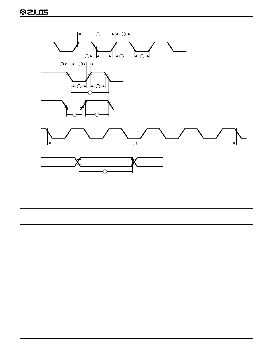
Clock
1
3
4
8
2
2
3
T
IRQ
IN
N
6
5
7
7
11
Clock
Setup
10
9
Source
AC ELECTRICAL CHARACTERISTICS
T
A
= 0
∞
C To +70
∞
C
8 MHz
12 MHz
V
CC
(E03)
(E06)
No Symbol Parameter
Note[3]
Min
Max
Min
Max
Units
Notes
1
TpC
Input Clock Period
5.0V
125
DC
83
DC
ns
[1,7,8]
2
TrC,TfC
Clock Input Rise
5.0V
25
15
ns
[1,7,8]
3
TwC
Input Clock Width
5.0V
62
41
ns
[1,7,8]
4
TwTinL
Timer Input Low Width
5.0V
70
70
ns
[1,7,8]
5
TwTinH
Timer Input High Width 5.0V
5TpC
5TpC
[1,7,8]
Additional Timing
AC ELECTRICAL CHARACTERISTICS
8
Z86E03/E06
CP95DZ81301
P R E L I M I N A R Y
AC ELECTRICAL CHARACTERISTICS
(Continued)
T
A
= 0
∞
C To +70
∞
C
8 MHz
12 MHz
V
CC
(E03)
(E06)
No Symbol Parameter
Note[3]
Min
Max
Min
Max
Units
Notes
6
TpTin
Timer Input Period
5.0V
8TpC
8TpC
[1,7,8]
7
TrTin,
Timer Input Rise
5.0V
100
100
ns
[1,7]
TtTin
and Fall Timer
8
TwIL
Int. Request Input
5.0V
70
70
ns
[1,2,7]
Low Time
9
TwIH
Int. Request Input
5.0V
5TpC
5TpC
[1,8,10]
High Time
10
Twsm
STOP Mode Recovery
5.0V
20
20
ns
[1]
Width Spec
11
Tost
Oscillator Startup Time
5.0V
5TpC
5TpC
ms
[1,4,9]
12
Twdt
Watch-Dog Timer
5.0V
6
6
ms
D1 = 0 [5,6]
Refresh Time
5.0V
12
12
ms
D1 = 0 [5,6]
5.0V
25
25
ms
D1 = 1 [5,6]
5.0V
100
100
ms
D1 = 1 [5,6]
Notes:
[1] Timing Reference uses 0.7 V
CC
for a logic 1 and 0.2 V
CC
for a logic 0.
[2] Interrupt request through Port 3 (P33-P31).
[3] V
CC
= 4.5V to 5.5V.
[4] SMR-D5 = 0, POR delay is off.
[5] Reg. WDTMR.
[6] Internal RC oscillator only.
[7] SMR D1 = 0.
[8] Maximum frequency for internal system clock is 4 MHz when using
SCLK = external clock.
[9] For RC and LC oscillator and for clock driven oscillator.
[10] SMR-D5 = 1, STOP mode recovery delay is on.

9
Z86E03/E06
CP95DZ81301
P R E L I M I N A R Y
Zilog's products are not authorized for use as critical compo-
nents in life support devices or systems unless a specific written
agreement pertaining to such intended use is executed between
the customer and Zilog prior to use. Life support devices or
systems are those which are intended for surgical implantation
into the body, or which sustains life whose failure to perform,
when properly used in accordance with instructions for use
provided in the labeling, can be reasonably expected to result in
significant injury to the user.
Zilog, Inc. 210 East Hacienda Ave.
Campbell, CA 95008-6600
Telephone (408) 370-8000
Telex 910-338-7621
FAX 408 370-8056
Internet: http://www.zilog.com
© 1994 by Zilog, Inc. All rights reserved. No part of this document
may be copied or reproduced in any form or by any means
without the prior written consent of Zilog, Inc. The information in
this document is subject to change without notice. Devices sold
by Zilog, Inc. are covered by warranty and patent indemnification
provisions appearing in Zilog, Inc. Terms and Conditions of Sale
only. Zilog, Inc. makes no warranty, express, statutory, implied or
by description, regarding the information set forth herein or
regarding the freedom of the described devices from intellectual
property infringement. Zilog, Inc. makes no warranty of mer-
chantability or fitness for any purpose. Zilog, Inc. shall not be
responsible for any errors that may appear in this document.
Zilog, Inc. makes no commitment to update or keep current the
information contained in this document.