 | –≠–ª–µ–∫—Ç—Ä–æ–Ω–Ω—ã–π –∫–æ–º–ø–æ–Ω–µ–Ω—Ç: Z86E23 | –°–∫–∞—á–∞—Ç—å:  PDF PDF  ZIP ZIP |
1
Z86E23
CPS DC-4060-06
C
USTOMER
P
ROCUREMENT
S
PECIFICATION
DC-4060-06
(3-22-94)
GENERAL DESCRIPTION
Z86E23
CMOS Z8
Æ
OTP
M
ICROCONTROLLER
The Z86E23 microcontroller introduces the next level of
sophistication to single-chip architecture. The Z86E23 is
a member of the Z8 single-chip microcontroller family with
8 Kbytes of EPROM and 236 bytes of general-purpose
RAM.
The Z86E23 is a pin compatible, One-Time-Programmable
(OTP) version of the Z8614 and Z8602 Keyboard Control-
ler (KBC).
Zilog's CMOS microcontroller offers fast execution, effi-
cient use of memory, sophisticated interrupts, input/output
bit manipulation capabilities, and easy hardware/software
system expansion along with low cost and low power
consumption.
The Z86E23 architecture is based on Zilog's 8-bit
microcontroller core. The device offers a flexible I/O
scheme, an efficient register and address space structure,
and a number of ancillary features that are useful in many
industrial and advanced scientific applications.
There are two basic address spaces available to support
this wide range of configurations: program memory and
236 general-purpose registers.
To unburden the program from coping with real-time
problems such as counting/timing, the Z86E23 offers two
on-chip counter/timers with a large number of user select-
able modes (Block Diagram).
Notes:
All Signals with a preceding front slash, "/", are active Low, e.g.,
B//W (WORD is active Low); /B/W (BYTE is active Low, only).
Power connections follow conventional descriptions below:
Connection
Circuit
Device
Power
V
CC
V
DD
Ground
GND
V
SS
2
Z86E23
CPS DC-4060-06
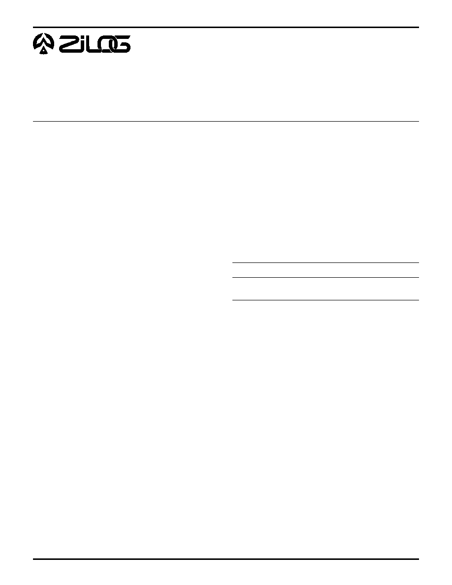
GENERAL DESCRIPTION (Continued)
Port 3
Interrupt
Control
Port 2
I/O
(Bit Programmable)
ALU
FLAGS
Register
Pointer
Register File
256 x 8-Bit
Machine Timing and
Instruction Control
Prg. Memory
8192 x 8-Bit
Program
Counter
Vcc
GND
4
4
Port 0
Output
Input
I/O
(Nibble Programmable)
Output Open Drain
8
Port 1
I/O
(Byte Programmable)
Output Open Drain
/RESET
XTAL
Counter/
Timers (2)
Functional Block Diagram
3
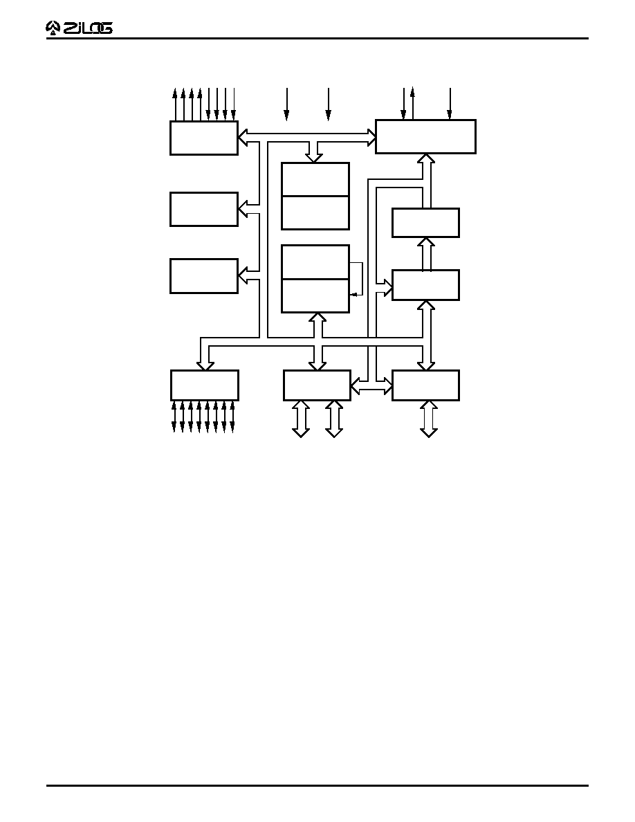
Z86E23
CPS DC-4060-06
1
2
9
3
4
5
6
7
8
40
39
38
37
36
35
34
33
32
NC
/OE
A9
/PGM
NC
NC
A12
A11
A10
VCC
NC
NC
/CE
/RESET
R//W*
/DS*
31
30
29
28
27
14
10
11
12
13
XTAL1
GND
EPM
A0
A1
A8
GND
NC
D7
D6
Z86E23
DIP
15
26
25
24
23
22
21
20
16
17
18
19
VPP
NC
A2
A3
A6
A7
A5
A4
D3
D5
D4
D2
D1
D0
40-Pin DIP Pin Assignments

4
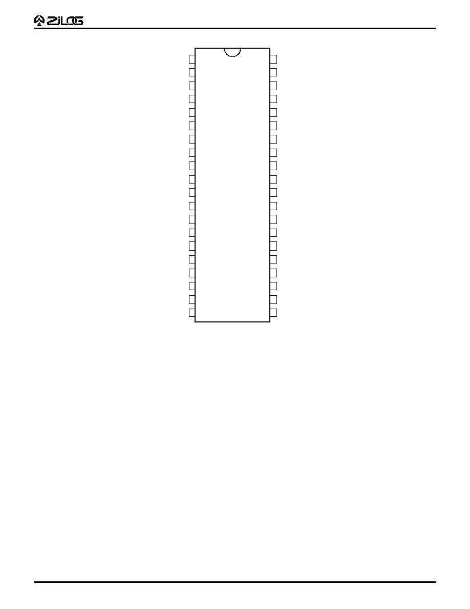
Z86E23
CPS DC-4060-06
NC
P30
P37
XTAL1
XTAL2
VCC
P36
P31
P27
P26
P25
P03
P04
P05
P06
P07
P10
P11
P12
P13
P14
NC
NC
P24
P23
P22
P21
P20
P33
P34
P17
P16
P15
/RESET
R//W*
/DS*
GND
P35
GND
P32
P00
P01
P02
R/RL
7
8
9
10
11
12
13
14
15
16
17
38
37
36
35
34
33
32
31
30
29
39
Z86E23
PLCC
6
5
4
3
2
1
44 43 42 41 40
18 19 20 21 22 23 24 25 26 27 28
44-Pin PLCC Pin Assignments
PIN DESCRIPTIONS
5
Z86E23
CPS DC-4060-06
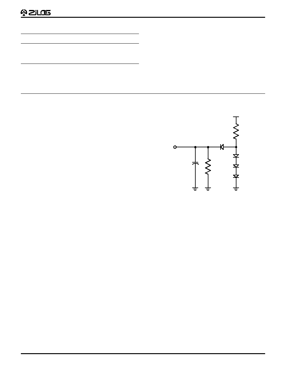
Test Load Diagram
ABSOLUTE MAXIMUM RATINGS
Symbol Description
Min
Max
Units
V
CC
Supply Voltage*
≠0.3
+7.0
V
T
STG
Storage Temp
≠65
+150
C
T
A
Oper Ambient Temp
C
Notes:
* Voltages on all pins with respect to GND.
13.0 V Maximum on P33-P30.
See Ordering Information
STANDARD TEST CONDITIONS
The characteristics listed below apply for standard test
conditions as noted. All voltages are referenced to GND.
Positive current flows into the referenced pin (Standard
Test Load).
Stresses greater than those listed under Absolute Maxi-
mum Ratings may cause permanent damage to the de-
vice. This is a stress rating only; operation of the device at
any condition above those indicated in the operational
sections of these specifications is not implied. Exposure to
absolute maximum rating conditions for an extended pe-
riod may affect device reliability.
+5V
From Output
Under Test
2.3 k
1.0 k
150 pF
6
Z86E23
CPS DC-4060-06
DC CHARACTERISTICS
V
CC
= 4.5 V to 5.5V @ 0
∞
C to +70
∞
C
Sym
Parameter
Min
Max
Typ*
Unit
Condition
V
CH
Clock Input High Voltage
3.8
V
CC
V
Driven by External Clock Generator
V
CL
Clock Input Low Voltage
≠0.3
0.8
V
Driven by External Clock Generator
V
IH
Input High Voltage
2.0
V
CC
V
V
IL
Input Low Voltage
≠0.3
0.8
V
V
RH
Reset Input High Voltage
3.8
V
CC
V
V
RL
Reset Input Low Voltage
≠0.3
0.8
V
V
OH
Output High Voltage
2.0
V
I
OH
= ≠250
µ
A (Port 2 only)
Output High Voltage
2.4
V
I
O H
= ≠250
µ
A (Port 3 only)
V
OL
Output Low Voltage
0.8
V
I
OL
= +4.0 mA (See Note (1) below.)
I
IL
Input Leakage
≠10
10
µ
A
V
IN
= 0V, 5.5V
I
OL
Output Leakage
≠10
10
µ
A
V
IN
= 0V, 5.5V
I
IR
Reset Input Current
≠50
µ
A
V
IN
= 0V, 5.5V
I
CC
V
CC
Supply Current
50
25
mA
Notes:
* Typical @ 25
∞
C
1. A combined total of six I/O pins from Ports 2 and 3 may be used to sink
10 mA each at 0.8V V
OL
(max. three pins per port). These may be used
for LEDs or as general-purpose outputs requiring high sink current.
Zilog's products are not authorized for use as critical compo-
nents in life support devices or systems unless a specific written
agreement pertaining to such intended use is executed between
the customer and Zilog prior to use. Life support devices or
systems are those which are intended for surgical implantation
into the body, or which sustains life whose failure to perform,
when properly used in accordance with instructions for use
provided in the labeling, can be reasonably expected to result in
significant injury to the user.
Zilog, Inc. 210 East Hacienda Ave.
Campbell, CA 95008-6600
Telephone (408) 370-8000
Telex 910-338-7621
FAX 408 370-8056
© 1994 by Zilog, Inc. All rights reserved. No part of this document
may be copied or reproduced in any form or by any means
without the prior written consent of Zilog, Inc. The information in
this document is subject to change without notice. Devices sold
by Zilog, Inc. are covered by warranty and patent indemnification
provisions appearing in Zilog, Inc. Terms and Conditions of Sale
only. Zilog, Inc. makes no warranty, express, statutory, implied or
by description, regarding the information set forth herein or
regarding the freedom of the described devices from intellectual
property infringement. Zilog, Inc. makes no warranty of mer-
chantability or fitness for any purpose. Zilog, Inc. shall not be
responsible for any errors that may appear in this document.
Zilog, Inc. makes no commitment to update or keep current the
information contained in this document.