 | –≠–ª–µ–∫—Ç—Ä–æ–Ω–Ω—ã–π –∫–æ–º–ø–æ–Ω–µ–Ω—Ç: Z86E33 | –°–∫–∞—á–∞—Ç—å:  PDF PDF  ZIP ZIP |

CP97DZ83300
P R E L I M I N A R Y
1
1
P
RELIMINARY
C
USTOMER
P
ROCUREMENT
S
PECIFICATION
Z86E33/733/E34
Z86E43/743/E44
1
CMOS Z8
Æ
OTP M
ICROCONTROLLERS
FEATURES
s
Standard Temperature (V
CC
= 3.5V to 5.5V)
s
Extended Temperature (V
CC
= 4.5V to 5.5V)
s
28-Pin DIP/SOIC/PLCC Packages (E33/733/E34)
40-Pin DIP Package (E43/743/E44)
44-Pin PLCC/QFP Packages (E43/743/E44)
s
Software Enabled Watch-Dog Timer (WDT)
s
Push-Pull/Open-Drain Programmable on
Port 0, Port 1, and Port 2
s
Low-Power Consumption: 60 mW
s
Programmable Crystal Oscillator, EPROM Protect,
RAM Protect, Auto Latch Disable, Permanent WDT,
32 KHz Oscillator, and EPROM /Test Mode Disable
s
Fast Instruction Pointer: 0.6
µ
s
s
Two Standby Modes: STOP and HALT
s
24/32 Input and Output Lines
s
Digital Inputs CMOS Levels, Schmitt-Triggered
s
Software Programmable Low EMI Mode
s
Two Programmable 8-Bit Counter/Timers Each with a 6-
Bit Programmable Prescaler
s
Six Vectored, Priority Interrupts from Six Different
Sources
s
Auto Latches
s
Auto Power-On Reset (POR)
s
Two Comparators
s
On-Chip Oscillator that Accepts a Crystal, Ceramic
Resonator, LC, RC, or External Clock Drive
GENERAL DESCRIPTION
The Z86E33/733/E34/E43/743/E44 8-bit CMOS One-Time
Programmable (OTP) microcontrollers are members of
Zilog's Z8
Æ
single-chip microcontroller family featuring en-
hanced wake-up circuitry, programmable Watch-Dog Tim-
ers, Low Noise EMI options, and easy hardware/software
system expansion capability.
Four basic address spaces support a wide range of mem-
ory configurations. The designer has easy access to regis-
ter mapped peripheral and I/O circuits.
For applications demanding powerful I/O capabilities, the
Z86E33/733/E34 have 24 pins and the Z86E43/743/E44
have 32 pins of dedicated input and output. These lines are
grouped into four ports, eight lines per port, and are config-
urable under software control to provide timing, status sig-
nals, and parallel I/O with or without handshake, and ad-
dress/data bus for interfacing external memory.
Notes:
All Signals with a preceding front slash, "/", are
active Low, e.g., B//W (WORD is active Low); /B/W (BYTE
is active Low, only).
Device
ROM
(KBytes)
RAM*
(Bytes)
I/O
Lines
Speed
(MHz)
Z86E33
4
237
24
16
Z86733
8
237
24
16
Z86E34
16
237
24
16
Z86E43
4
236
32
16
Z86743
8
236
32
16
Z86E44
16
236
32
16
Note:
*General-Purpose
Z86E33/733/E34/E43/743/E44
CMOS Z8Æ OTP Microcontrollers
Zilog
2
P R E L I M I N A R Y
CP97DZ83300
Power connections follow conventional descriptions be-
low:
Connection
Circuit
Device
Power
V
CC
V
DD
Ground
GND
V
SS
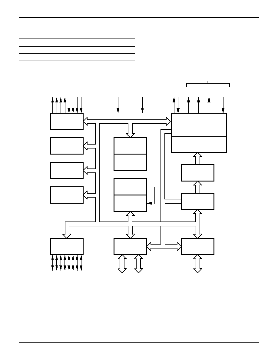
Figure 1. Functional Block Diagram
Port 3
Counter/
Timers (2)
Interrupt
Control
Two Analog
Comparators
Port 2
I/O
(Bit Programmable)
ALU
FLAGS
Machine Timing
&
Instruction Control
Program
Counter
VCC
GND
XTAL
4
4
Port 0
Output
Input
Address or I/O
(Nibble Programmable)
8
Address/Data or I/O
(Byte Programmable)
/AS /DS R//W /RESET
RESET
WDT, POR
Port 1
OTP
Register File
Register
Pointer
(E43/743/E44)
(E43/743/E44 Only)
Z86E33/733/E34/E43/743/E44
Zilog
CMOS Z8Æ OTP Microcontrollers
CP97DZ83300
P R E L I M I N A R Y
3
1
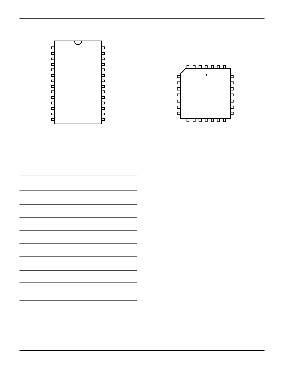
PIN IDENTIFICATION
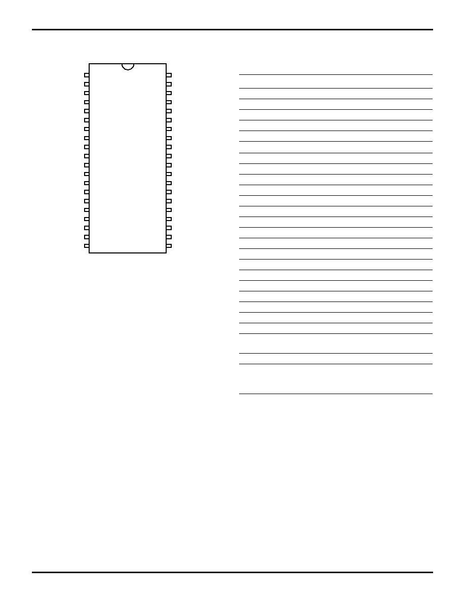
Figure 2. 40-Pin DIP Pin Configuration
Standard Mode
R//W
P25
P26
P27
P04
P05
P06
P14
P15
P07
VCC
P16
P17
XTAL2
XTAL1
P31
P32
P33
P34
/AS
/DS
P24
P23
P22
P21
P20
P03
P13
P12
GND
P02
P11
P10
P01
P00
P30
P36
P37
P35
/RESET
40
DIP
1
20
21
Table 1. 40-Pin DIP Pin Identification
Standard Mode
Pin #
Symbol
Function
Direction
1
R//W
Read/Write
Output
2-4
P25-P27
Port 2, Pins 5,6,7 In/Output
5-7
P04-P06
Port 0, Pins 4,5,6 In/Output
8-9
P14-P15
Port 1, Pins 4,5
In/Output
10
P07
Port 0, Pin 7
In/Output
11
V
CC
Power Supply
12-13
P16-P17
Port 1, Pins 6,7
In/Output
14
XTAL2
Crystal Oscillator Output
15
XTAL1
Crystal Oscillator Input
16-18
P31-P33
Port 3, Pins 1,2,3 Input
19
P34
Port 3, Pin 4
Output
20
/AS
Address Strobe
Output
21
/RESET
Reset
Input
22
P35
Port 3, Pin 5
Output
23
P37
Port 3, Pin 7
Output
24
P36
Port 3, Pin 6
Output
25
P30
Port 3, Pin 0
Input
26-27
P00-P01
Port 0, Pins 0,1
In/Output
28-29
P10-P11
Port 1, Pins 0,1
In/Output
30
P02
Port 0, Pin 2
In/Output
31
GND
Ground
32-33
P12-P13
Port 1, Pins 2,3
In/Output
34
P03
Port 0, Pin 3
In/Output
35-39
P20-P24
Port 2, Pins
0,1,2,3,4
In/Output
40
DS
Data Strobe
Output
Notes:
Pin Configuration and Identification identical on DIP
and Cerdip Window Lid style packages.
Z86E33/733/E34/E43/743/E44
CMOS Z8Æ OTP Microcontrollers
Zilog
4
P R E L I M I N A R Y
CP97DZ83300
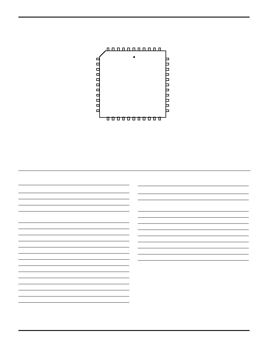
Figure 3. 44-Pin PLCC Pin Configuration
Standard Mode
PLCC 44 - Pin
7
17
P21
P22
P23
P24
/DS
NC
R//W
P25
P26
P27
P04
P30
P36
P37
P35
/RESET
R//RL
/AS
P34
P33
P32
P31
P05
P06
P14
P15
P07
VCC
VCC
P16
P17
XT
AL2
XT
AL1
P20
P03
P13
P12
GND
GND
P02
P11
P10
P01
P00
1
28
18
40
39
29
6
Table 2. 44-Pin PLCC Pin Identification
Pin #
Symbol
Function
Direction
1-2
GND
Ground
3-4
P12-P13
Port 1, Pins 2,3 In/Output
5
P03
Port 0, Pin 3
In/Output
6-10
P20-P24
Port 2, Pins
0,1,2,3,4
In/Output
11
/DS
Data Strobe
Output
12
NC
No Connection
13
R//W
Read/Write
Output
14-16
P25-P27
Port 2, Pins 5,6,7In/Output
17-19
P04-P06
Port 0, Pins 4,5,6In/Output
20-21
P14-P05
Port 1, Pins 4,5 In/Output
22
P07
Port 0, Pin 7
In/Output
23-24
VCC
Power Supply
25-26
P16-P17
Port 1, Pins 6,7 In/Output
27
XTAL2
Crystal Oscillator Output
28
XTAL1
Crystal Oscillator Input
29-31
P31-P33
Port 3, Pins 1,2,3Input
32
P34
Port 3, Pin 4
Output
33
/AS
Address Strobe Output
34
R//RL
ROM/ROMless
select
Input
35
/RESET
Reset
Input
36
P35
Port 3, Pin 5
Output
37
P37
Port 3, Pin 7
Output
38
P36
Port 3, Pin 6
Output
39
P30
Port 3, Pin 0
Input
40-41
P00-P01
Port 0, Pins 0,1 In/Output
42-43
P10-P11
Port 1, Pins 0,1 In/Output
44
P02
Port 0, Pin 2
In/Output
Table 2. 44-Pin PLCC Pin Identification
Pin #
Symbol
Function
Direction
Z86E33/733/E34/E43/743/E44
Zilog
CMOS Z8Æ OTP Microcontrollers
CP97DZ83300
P R E L I M I N A R Y
5
1
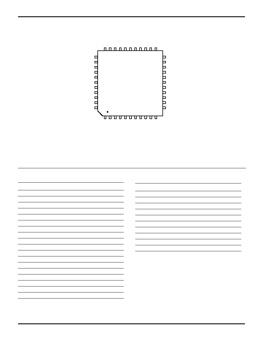
Figure 4. 44-Pin QFP Pin Configuration
Standard Mode
34
44
P21
P22
P23
P24
/DS
NC
R//W
P25
P26
P27
P04
P30
P36
P37
P35
/RESET
R//RL
/AS
P34
P33
P32
P31
P05
P06
P14
P15
P07
VCC
VCC
P16
P17
XT
AL2
XT
AL1
P20
P03
P13
P12
GND
GND
P02
P11
P10
P01
P00
1
23
33
QFP 44 - Pin
11
22
12
Table 3. 44-Pin QFP Pin Identification
Pin #
Symbol Function
Direction
1-2
P05-P06 Port 0, Pins 5,6
In/Output
3-4
P14-P05 Port 1, Pins 4,5
In/Output
5
P07
Port 0, Pin 7
In/Output
6-7
VCC
Power Supply
8-9
P16-P17 Port 1, Pins 6,7
In/Output
10
XTAL2
Crystal Oscillator
Output
11
XTAL1
Crystal Oscillator
Input
12-14
P31-P13 Port 3, Pins 1,2,3
Input
15
P34
Port 3, Pin 4
Output
16
/AS
Address Strobe
Output
17
R//RL
ROM/ROMless select Input
18
/RESET Reset
Input
19
P35
Port 3, Pin 5
Output
20
P37
Port 3, Pin 7
Output
21
P36
Port 3, Pin 6
Output
22
P30
Port 3, Pin 0
Input
23-24
P00-P01 Port 0, Pins 0,1
In/Output
25-26
P10-P11 Port 1, Pins 0,1
In/Output
27
P02
Port 0, Pin 2
In/Output
28-29
GND
Ground
30-31
P12-P13 Port 1, Pins 2,3
In/Output
32
P03
Port 0, Pin 3
In/Output
33-37
P20-4
Port 2, Pins 0,1,2,3,4 In/Output
38
/DS
Data Strobe
Output
39
NC
No Connection
40
R//W
Read/Write
Output
41-43
P25-P27 Port 2, Pins 5,6,7
In/Output
44
P04
Port 0, Pin 4
In/Output
Table 3. 44-Pin QFP Pin Identification
Pin #
Symbol Function
Direction
Z86E33/733/E34/E43/743/E44
CMOS Z8Æ OTP Microcontrollers
Zilog
6
P R E L I M I N A R Y
CP97DZ83300
Figure 5. Standard Mode
28-Pin DIP/SOIC Pin Configuration
Table 4. 28-Pin DIP/SOIC/PLCC
Pin Identification
Pin #
Symbol
Function
Direction
1-3
P25-P27
Port 2, Pins 5,6,7
In/Output
4-7
P04-P07
Port 0, Pins 4,5,6,7 In/Output
8
V
CC
Power Supply
9
XTAL2
Crystal Oscillator
Output
10
XTAL1
Crystal Oscillator
Input
11-13
P31-P33
Port 3, Pins 1,2,3
Input
14-15
P34-P35
Port 3, Pins 4,5
Output
16
P37
Port 3, Pin 7
Output
17
P36
Port 3, Pin 6
Output
18
P30
Port 3, Pin 0
Input
19-21
P00-P02
Port 0, Pins 0,1,2
In/Output
22
V
SS
Ground
23
P03
Port 0, Pin 3
In/Output
24-28
P20-P24
Port 2, Pins
0,1,2,3,4
In/Output
Notes:
Pin Identification and Configuration identical on DIP and
Cerdip Window Lid style packages.
P25
P26
P27
P04
P05
P06
P07
VCC
XTAL2
XTAL1
P31
P32
P33
P34
P24
P23
P22
P21
P20
P03
VSS
P02
P01
P00
P30
P36
P37
P35
15
DIP 28 - Pin
1
14
28
Figure 6. Standard Mode
28-Pin PLCC Pin Configuration
25
19
5
11
18
12
26
4
PLCC 28 - Pin
1
XXX
XXX
XXX
XXX
XXX
XXX
XXX
XXX
XXX
XXX
XXX
XXX
XXX
XXX
P21
P20
P03
VSS
P02
P01
P00
P05
P06
P07
VCC
XT2
XT1
P31
P04
P27
P26
P25
P24
P23
P22
P32
P33
P34
P35
P37
P36
P30
Z86E33/733/E34/E43/743/E44
Zilog
CMOS Z8Æ OTP Microcontrollers
CP97DZ83300
P R E L I M I N A R Y
7
1
ABSOLUTE MAXIMUM RATINGS
Stresses greater than those listed under Absolute Maxi-
mum Ratings may cause permanent damage to the de-
vice. This is a stress rating only; functional operation of the
device at any condition above those indicated in the oper-
ational sections of these specifications is not implied. Ex-
posure to absolute maximum rating conditions for an ex-
tended period may affect device reliability.
Total power dissipation should not exceed 1.2 W for the
package. Power dissipation is calculated as follows:
Total Power Dissipation = V
DD
x [ I
DD
≠ (sum of I
OH
) ]
+ sum of [ (V
DD
≠ V
OH
) x I
OH
]
+ sum of (V
0L
x I
0L
)
STANDARD TEST CONDITIONS
The characteristics listed below apply for standard test
conditions as noted. All voltages are referenced to
Ground. Positive current flows into the referenced pin
(Test Load).
Parameter
Min
Max
Units
Ambient Temperature under Bias
≠40
+105
C
Storage Temperature
≠65
+150
C
Voltage on any Pin with Respect to V
SS
[Note 1]
≠0.6
+7
V
Voltage on V
DD
Pin with Respect to V
SS
≠0.3
+7
V
Voltage on XTAL1 and /RESET Pins with Respect to V
SS
[Note 2]
≠0.6
V
DD
+1
V
Total Power Dissipation
1.21
W
Maximum Allowable Current out of V
SS
220
mA
Maximum Allowable Current into V
DD
180
mA
Maximum Allowable Current into an Input Pin [Note 3]
≠600
+600
µ
A
Maximum Allowable Current into an Open-Drain Pin [Note 4]
≠600
+600
µ
A
Maximum Allowable Output Current Sinked by Any I/O Pin
25
mA
Maximum Allowable Output Current Sourced by Any I/O Pin
25
mA
Notes:
1. This applies to all pins except XTAL pins and where otherwise noted.
2. There is no input protection diode from pin to V
DD
.
3. This excludes XTAL pins.
4. Device pin is not at an output Low state.
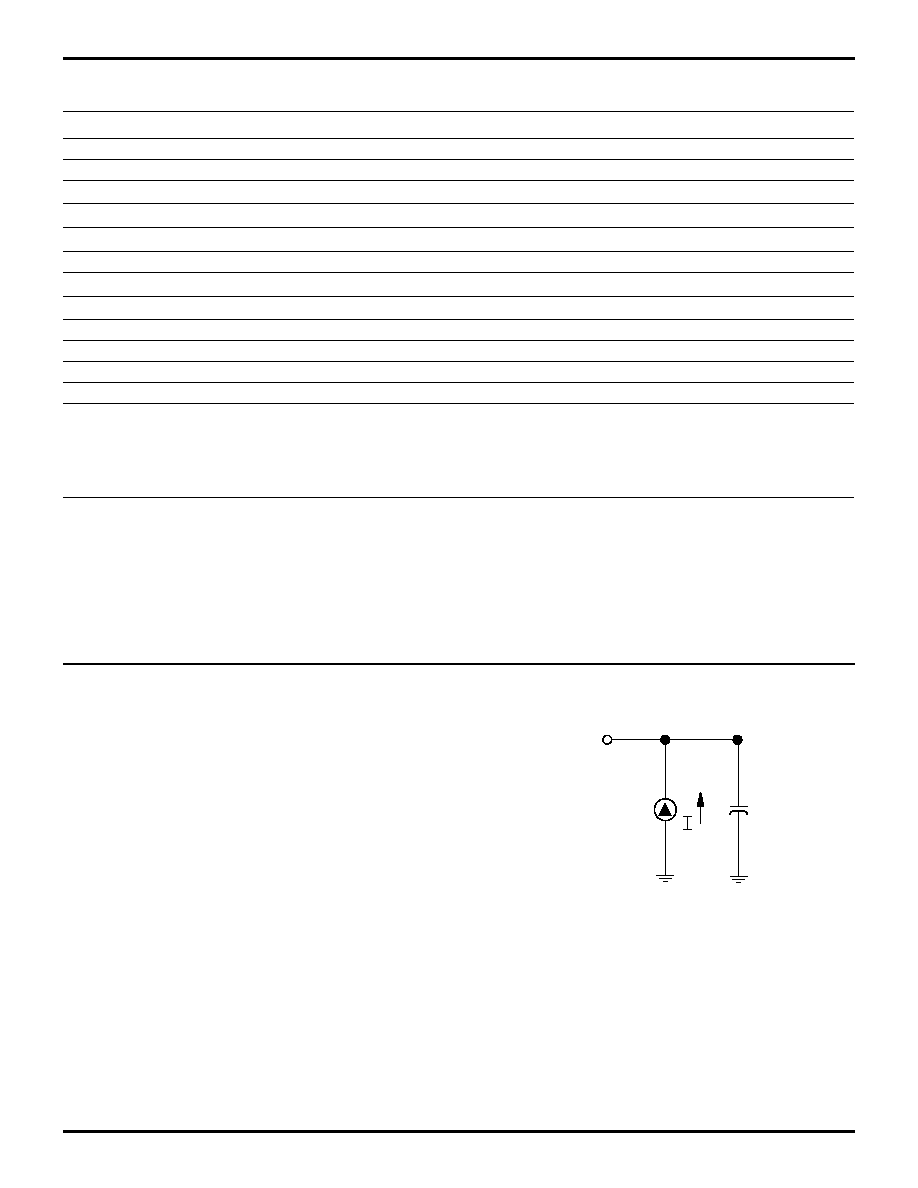
Figure 7. Test Load Diagram
150 pF
From Output
Under Test

Z86E33/733/E34/E43/743/E44
CMOS Z8Æ OTP Microcontrollers
Zilog
8
P R E L I M I N A R Y
CP97DZ83300
CAPACITANCE
T
A
= 25
∞
C, V
CC
= GND = 0V, f = 1.0 MHz; unmeasured pins returned to GND.
Parameter
Min
Max
Input capacitance
0
12 pF
Output capacitance
0
12 pF
I/O capacitance
0
12 pF

Z86E33/733/E34/E43/743/E44
Zilog
CMOS Z8Æ OTP Microcontrollers
CP97DZ83300
P R E L I M I N A R Y
9
1
© 1997 by Zilog, Inc. All rights reserved. No part of this
document may be copied or reproduced in any form or by
any means without the prior written consent of Zilog, Inc.
The information in this document is subject to change
without notice. Devices sold by Zilog, Inc. are covered by
warranty and patent indemnification provisions appearing
in Zilog, Inc. Terms and Conditions of Sale only. Zilog, Inc.
makes no warranty, express, statutory, implied or by
description, regarding the information set forth herein or
regarding the freedom of the described devices from
intellectual property infringement. Zilog, Inc. makes no
warranty of merchantability or fitness for any purpose.
Zilog, Inc. shall not be responsible for any errors that may
appear in this document. Zilog, Inc. makes no commitment
to update or keep current the information contained in this
document.
Zilog's products are not authorized for use as critical
components in life support devices or systems unless a
specific written agreement pertaining to such intended use
is executed between the customer and Zilog prior to use.
Life support devices or systems are those which are
intended for surgical implantation into the body, or which
sustains life whose failure to perform, when properly used
in accordance with instructions for use provided in the
labeling, can be reasonably expected to result in
significant injury to the user.
Zilog, Inc. 210 East Hacienda Ave.
Campbell, CA 95008-6600
Telephone (408) 370-8000
FAX 408 370-8056
Internet: http://www.zilog.com

Z86E33/733/E34/E43/743/E44
CMOS Z8Æ OTP Microcontrollers
Zilog
10
P R E L I M I N A R Y
CP97DZ83300