 | –≠–ª–µ–∫—Ç—Ä–æ–Ω–Ω—ã–π –∫–æ–º–ø–æ–Ω–µ–Ω—Ç: Z86E47 | –°–∫–∞—á–∞—Ç—å:  PDF PDF  ZIP ZIP |

1
Z86E47-ROM
CPS DC-4157-01
P R E L I M I N A R Y
GENERAL DESCRIPTION
The Z86E47 Digital Television Controller (DTC) introduce
a new level of sophistication to single-chip architecture.
The Z86E47 is a member of the Z8 single-chip
microcontroller family with 16 Kbytes of OTP (One-Time-
Programmable) ROM and 236 bytes of RAM. The device
is housed in a 64-pin DIP package, and is CMOS compat-
ible. The part features ROMs for program storage and
character generation. The Z86E47 microcontroller may be
used in prototyping, low volume applications or where
code development is required. Zilog's DTC offers fast
execution, efficient use of memory, sophisticated inter-
rupts, input/output bit manipulation capabilities, and easy
hardware/software system expansion along with low cost
and low power consumption. The device provides an ideal
performance and reliability solution for consumer and
industrial television applications.
The Z86E47 architecture utilizes Zilog's advanced
SuperintegrationTM design methodology. The device has
an 8-bit internal data path controlled by a Z8 microcontroller,
On-Screen Display (OSD) logic circuits/Pulse Width Modu-
lators (PWM). On-chip peripherals include five register/
memory mapped I/O ports (Ports 2, 3, 4, 5, and 6), Interrupt
control logic (1 software, 2 external and 3 internal inter-
rupts) and a standby mode recovery input port (Port 3, pin
P30).
The OSD control circuits support eight rows by 20 columns
for 128 kinds of characters. The character color is speci-
fied by row. One of the eight rows is assigned to show two
kinds of colors for bar type displays such as volume
control. The OSD is capable of displaying high resolution
(11x15 dot pattern) characters.
DC-4157-01
(2-18-94)
P
RELIMINARY
C
USTOMER
P
RODUCT
S
PECIFICATION
Z86E47 OTP ROM
CMOS Z8
Æ
8-B
IT
M
ICROCONTROLLER
A 14-bit PWM port provides enough voltage resolution for
a voltage synthesizer tuning system. Seven 6-bit PWM
ports are used for controlling audio signal level. Five 8-bit
PWM ports are used to vary picture levels.
DTC applications demand powerful I/O capabilities. The
Z86E47 fulfills this with 35 I/O pins dedicated to input and
output. These lines are grouped into five ports, and are
configurable under software control to provide timing,
status signals, parallel I/O and an address/data bus for
interfacing to external memory.
There are three basic address spaces available to support
this wide range of configurations: Program Memory, Reg-
ister File and Data Memory. The Data Memory address
space contains a number of control registers for the
PWMs, OSD, and I/O Ports 4, 5, and 6. Specifically, there
are 13 PWM and eight OSD control registers mapped into
the external memory address space. Three I/O registers
for Ports 4, 5, and 6 reside in data memory space as well.
The Register File is composed of 236 bytes of general
purpose register, two I/O Port registers and 15 control and
status registers.
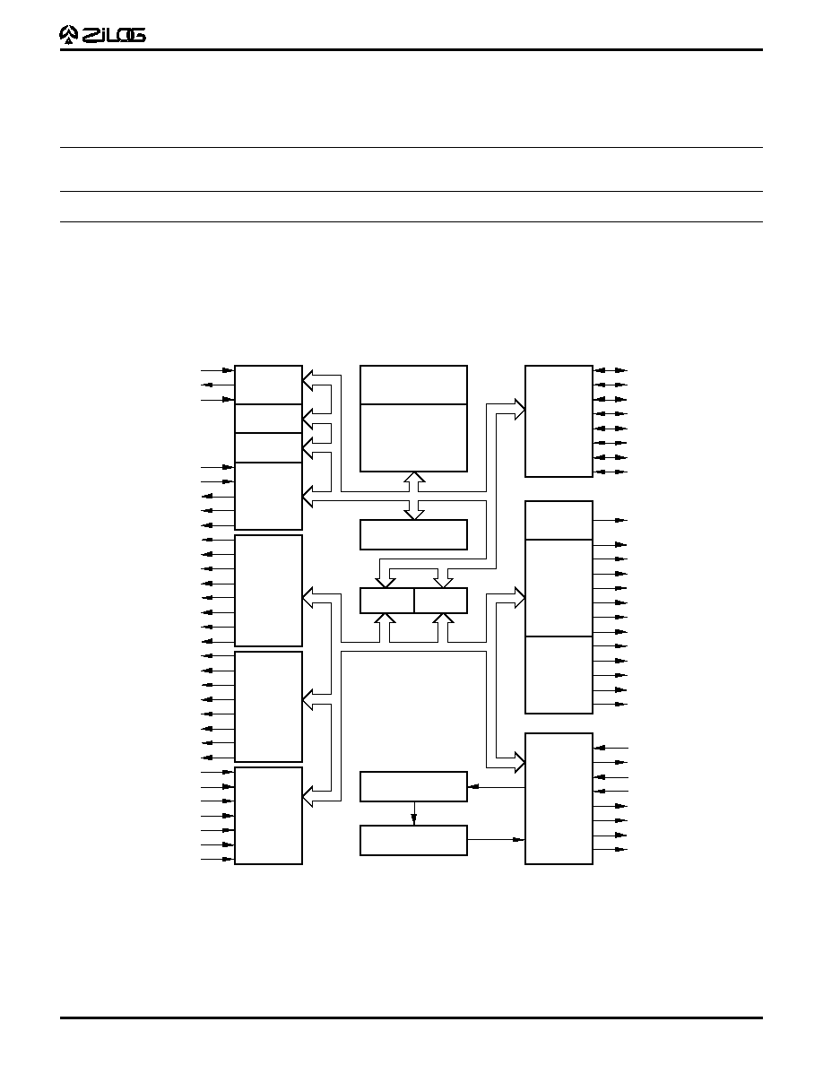
To unburden the program from coping with the real-time
problems such as counting/timing and data communica-
tion, the DTC's offer two on-chip counter/timers with a large
number of user selectable modes (see block diagram).
Note: All Signals with a preceding front slash, "/", are active
Low, e.g.: B//W (WORD is active Low); /B/W (BYTE is
active Low, only).
2
Z86E47-ROM
CPS DC-4157-01
P R E L I M I N A R Y
Counter
Timer
Counter
Timer
16K Byte
Program ROM
RESET
Oscillator
WDT
Port 3/
Interrupt
Port4
Port 5
Port 6
160 Byte
Character RAM
4 KByte
Character ROM
Z8 CPU
Core
Port 2
256 Byte
Register File
Port 1
A8:15
AD0:7
PWM 1
14 -bit
PWM 2
to
PWM 8
6-bit
PWM 9
to
PWM 13
8-bit
On Screen
Display
Port 0
P27
P26
P25
P24
P23
P22
P21
P20
PWM 1
PWM 2
PWM 3
PWM 4
PWM 5
PWM 6
PWM 7
PWM 8
PWM 9
PWM 10
PWM 11
PWM 12
PWM 13
OSCIN
OSCOUT
HSYNC
VSYNC
VRED
VGREEN
VBLUE
VBLANK
XTAL1
XTAL2
/RESET
P30
P31
P34
P35
P36
P40
P41
P42
P43
P44
P45
P46
P47
P50
P51
P52
P53
P54
P55
P56
P57
P60
P61
P62
P63
P64
P65
AFCIN
Functional Block Diagram
PRODUCT RECOMMENDATIONS
Zilog recommends the following programming equipment
for use with this one-time-programmable product.
Recommended
Device
Zilog Support Tool
Hardware
Z86E4700ZDP
Z86E47 Programming Adapter
A
Some non-Zilog programmers may have different pro-
gramming waveforms, voltages and timings and not all
programmers may meet the programming requirements of
Zilog's one-time-programmable products.
If difficulty is encountered in programming a Zilog OTP
product, please contact your local Zilog sales office.

3
Z86E47-ROM
CPS DC-4157-01
P R E L I M I N A R Y
PIN CONFIGURATION
PWM5
PWM4
PWM3
PWM2
PWM1
P35
P36
P34
P31
P30
XTAL1
XTAL2
/RESET
P60
GND
P61
P62
VCC
P63
P64
P65
AFCIN
P50
P51
P52
1
2
3
4
5
6
7
8
9
10
11
12
13
14
15
16
17
18
19
20
21
22
23
24
25
26
27
28
29
30
31
32
P53
P54
P55
P56
P57
OSCIN
OSCOUT
PWM6
PWM7
PWM8
PWM9
PWM10
PWM11
PWM12
PWM13
P27
P26
P25
P24
P23
GND
P22
VCC
P20
P47
P46
P45
P44
P43
P42
P41
P40
VBLANK
VBLUE
VGREEN
VRED
VSYNC
HSYNC
P21
64
63
62
61
60
59
58
56
55
54
53
52
51
50
49
48
47
46
45
44
43
42
41
40
39
38
37
36
35
34
33
57
Z86E47
Z86E47 OTP ROM Plastic DIP
4
Z86E47-ROM
CPS DC-4157-01
P R E L I M I N A R Y
Symbol
Parameters
Min
Max
Units
Notes
V
CC
Power Supply Voltage
≠0.3
+7
V
V
I
Input Voltage
≠0.3
V
CC
+ 0.3
V
V
I
Input Voltage
≠0.3
V
CC
+ 0.3
V
[1]
V
O
Output Voltage
≠0.3
V
CC
+ 8.0
V
[2]
I
OH
Output Current High
≠10
mA
1 pin
I
OH
Output Current High
≠100
mA
all total
I
OL
Output Current Low
20
mA
1 pin
I
OL
Output Current Low
40
mA
[3] (1 pin)
I
OL
Output Current Low,all total
200
mA
T
A
Operating Temperature
T
STG
Storage Temperature
≠65
+150
C
From Output
Under Test
RLL
VDD
RLH
150 pF
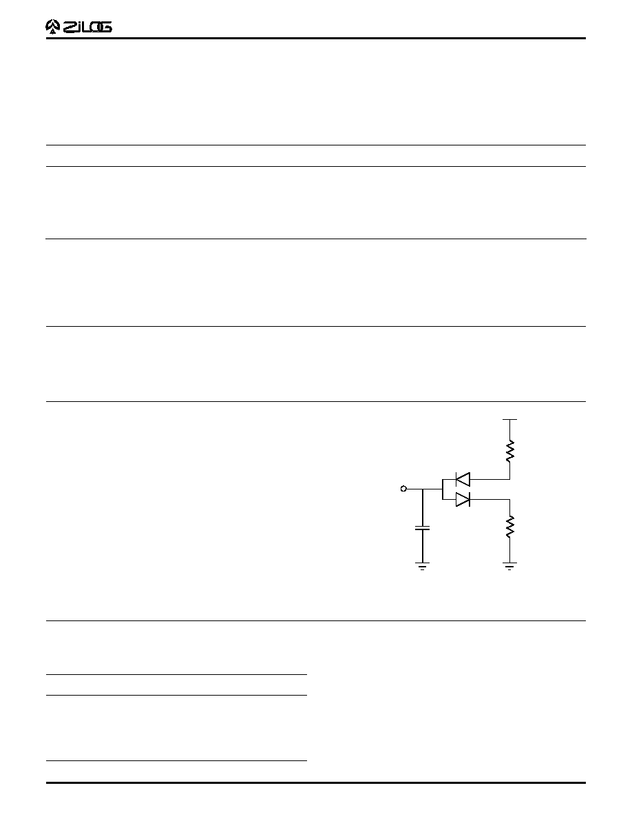
STANDARD TEST CONDITIONS
The characteristics listed below apply for standard test
conditions as noted. All voltages are referenced to GND.
Positive current flows into the referenced pin (see Test
Load Diagram).
Notes:
[1] Port 2 open-drain
[2] PWM open-drain outputs
[3] Port 5
Voltage on all pins with respect to GND.
See Ordering Information
CAPACITANCE
T
A
=25
∞
C, V
CC
=GND=0 V, Freq=1.0 MHz, unmeasured pins to GND.
Test Load Diagram
ABSOLUTE MAXIMUM RATINGS
Stress greater than those listed under Absolute Maximum
Ratings may cause permanent damage to the device. This
is a stress rating only; operation of the device at any
condition above those indicated in the operational sec-
tions of these specifications is not implied. Exposure to
absolute maximum rating conditions for extended periods
may affect device reliability.
Parameter
Max
Units
Input capacitance
10
pF
Output capacitance
20
pF
I/O capacitance
25
pF
AFC
IN
input capacitance
10
pF
5
Z86E47-ROM
CPS DC-4157-01
P R E L I M I N A R Y
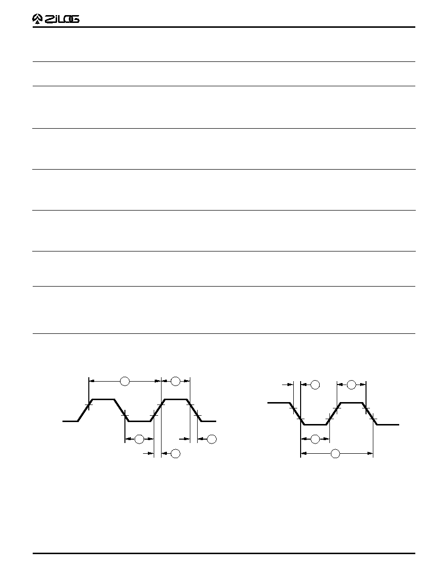
AC CHARACTERISTICS
Timing Diagrams
XTAL1
1
2
2
3
3
External Clock
Tin
7
5
4
6
Counter Timer
DC CHARACTERISTICS
T
A
=0
∞
C to +70
∞
C; V
CC
=+4.5 V to +5.5 V; F
OSC
=4 MHz
T
A
=0
∞
C to +70
∞
C
Typical
Symbol Parameter
Min
Max
@ 25
∞
C Units
Conditions
V
IL
Input Voltage Low
0
0.2 V
CC
1.48
V
V
ILC
Input XTAL/Osc In Low
0.07 V
CC
0.98
V
External Clock Generator Driven
V
IH
Input Voltage High
0.7 V
CC
V
CC
3.0
V
V
IHC
Input XTAL/Osc in High
0.8 V
CC
V
CC
3.2
V
External Clock Generator Driven
V
HY
Schmitt Hysteresis
0.1 V
CC
0.8
V
V
PU
Maximum Pull-up Voltage
12
V
[2]
V
OL
Output Voltage Low
0.4
0.16
V
I
OL
=1.00 mA
0.4
0.19
V
I
OL
=3.2 mA, [1]
0.4
0.19
V
I
OL
=0.75 mA [2]
1.5
1.00
V
I
OL
=10 mA [1]
V
00-01
AFC Level 01 In
0.45 V
CC
1.9
V
V
01-11
AFC Level 11 In
0.5 V
CC
0.75 V
CC
3.12
V
V
OH
Output Voltage High
V
CC
≠0.4
4.75
V
I
OH
= ≠0.75 mA
I
IR
Reset Input Current
≠80
≠46
µ
A
V
RL
=0 V
I
IL
Input Leakage
≠3.0
3.0
0.01
µ
A
0 V,V
CC
I
OL
Tri-State Leakage
≠3.0
3.0
0.02
µ
A
0 V,V
CC
I
CC
Supply Current
35
22
mA
All inputs at rail
I
CC1
6
3.2
mA
All inputs at rail
I
CC2
10
0
µ
A
All inputs at rail [3]
Notes:
[1] Port 5
[2] PWM Open-Drain
[3] XTAL1 Disconnected

6
Z86E47-ROM
CPS DC-4157-01
P R E L I M I N A R Y
IRQn
8
9
Interrupt Request
HSYNC
14
13
OSC2
On Screen Display
External /RESET
10
11
12
Internal /RESET
Vcc
Power On Reset

7
Z86E47-ROM
CPS DC-4157-01
P R E L I M I N A R Y
AC CHARACTERISTICS
T
A
=0
∞
C to +70
∞
C; V
CC
=+4.5 V to +5.5 V; F
OSC
=4 MHz,
No
Symbol
Parameter
Min
Max
Unit
1
TpC
Input clock period
250
1000
ns
2
TrC,TfC
Clock input raise and fall
15
ns
3
TwC
Input clock width
125
ns
4
TwTinL
Timer input low width
70
ns
5
TwTinH
Timer input high width
3 TpC
6
TpTin
Timer input period
8 TpC
7
TrTin,TfTin
Timer input raise and fall
100
ns
8A
TwIL
Int req input low
70
ns
8B
TwIL
3 TpC
9
TwIH
Int request input high
3 TpC
10
TdPOR
Power On Reset delay
25
100
ms
11
TdLVIRES
Low voltage detect to In-
200
ns
Internal RESET condition
12
TwRES
Reset minimum width
5 TpC
13
TdHsOI
Hsync start to Vosc stop
2 TpV
3 TpV
14
TdHsOh
Hsync end to Vosc start
1 TpV
15
TdWDT
WDT Refresh Time
12
ms
Notes:
[1] Refer to DC Characteristics for details on switching levels.
* Units in nanoseconds

8
Z86E47-ROM
CPS DC-4157-01
P R E L I M I N A R Y
Zilog's products are not authorized for use as critical compo-
nents in life support devices or systems unless a specific written
agreement pertaining to such intended use is executed between
the customer and Zilog prior to use. Life support devices or
systems are those which are intended for surgical implantation
into the body, or which sustains life whose failure to perform,
when properly used in accordance with instructions for use
provided in the labeling, can be reasonably expected to result in
significant injury to the user.
Zilog, Inc. 210 East Hacienda Ave.
Campbell, CA 95008-6600
Telephone (408) 370-8000
Telex 910-338-7621
FAX 408 370-8056
© 1993 by Zilog, Inc. All rights reserved. No part of this document
may be copied or reproduced in any form or by any means
without the prior written consent of Zilog, Inc. The information in
this document is subject to change without notice. Devices sold
by Zilog, Inc. are covered by warranty and patent indemnification
provisions appearing in Zilog, Inc. Terms and Conditions of Sale
only. Zilog, Inc. makes no warranty, express, statutory, implied or
by description, regarding the information set forth herein or
regarding the freedom of the described devices from intellectual
property infringement. Zilog, Inc. makes no warranty of mer-
chantability or fitness for any purpose. Zilog, Inc. shall not be
responsible for any errors that may appear in this document.
Zilog, Inc. makes no commitment to update or keep current the
information contained in this document.
Pre-Characterization Product:
The product represented by this CPS is newly introduced
and Zilog has not completed the full characterization of the
product. The CPS states what Zilog knows about this
product at this time, but additional features or non-con-
formance with some aspects of the CPS may be found,
either by Zilog or its customers in the course of further
application and characterization work. In addition, Zilog
cautions that delivery may be uncertain at times, due to
start-up yield issues.