
ZiLOG Worldwide Headquarters ∑ 910 E. Hamilton Avenue ∑ Campbell, CA 95008
Telephone: 408.558.8500 ∑ Fax: 408.558.8300 ∑
www.ZiLOG.com
Product Specification
PS014401-1001
Z86E61/Z86E63
CMOS Z8 16K/32K EPROM
Microcontroller

PS014401-1001
-
This publication is subject to replacement by a later edition. To determine whether a later edition exists, or to request
copies of publications, contact
ZiLOG Worldwide Headquarters
910 E. Hamilton Avenue
Campbell, CA 95008
Telephone: 408.558.8500
Fax: 408.558.8300
www.ZiLOG.com
Windows is a registered trademark of Microsoft Corporation.
Document Disclaimer
© 2001 by ZiLOG, Inc. All rights reserved. Information in this publication concerning the devices,
applications, or technology described is intended to suggest possible uses and may be superseded. ZiLOG,
INC. DOES NOT ASSUME LIABILITY FOR OR PROVIDE A REPRESENTATION OF ACCURACY OF
THE INFORMATION, DEVICES, OR TECHNOLOGY DESCRIBED IN THIS DOCUMENT. ZiLOG
ALSO DOES NOT ASSUME LIABILITY FOR INTELLECTUAL PROPERTY INFRINGEMENT
RELATED IN ANY MANNER TO USE OF INFORMATION, DEVICES, OR TECHNOLOGY
DESCRIBED HEREIN OR OTHERWISE. Except with the express written approval ZiLOG, use of
information, devices, or technology as critical components of life support systems is not authorized. No
licenses or other rights are conveyed, implicitly or otherwise, by this document under any intellectual property
rights.

Z86E61/E63
CMOS Z8 16K/32K EPROM Microcontroller
PS014401-1001
iii
Table of Contents
FEATURES . . . . . . . . . . . . . . . . . . . . . . . . . . . . . . . . . . . . . . . . . . . . . . . . . . . . . 1
GENERAL DESCRIPTION . . . . . . . . . . . . . . . . . . . . . . . . . . . . . . . . . . . . . . . . . 2
PIN FUNCTIONS . . . . . . . . . . . . . . . . . . . . . . . . . . . . . . . . . . . . . . . . . . . . . . . 11
ROMless (Input, Active Low). . . . . . . . . . . . . . . . . . . . . . . . . . . . . . . . . . . . 11
DS (Output, Active Low). . . . . . . . . . . . . . . . . . . . . . . . . . . . . . . . . . . . . . . . 11
AS (Output, Active Low). . . . . . . . . . . . . . . . . . . . . . . . . . . . . . . . . . . . . . . . 11
XTAL2, XTAL1 . . . . . . . . . . . . . . . . . . . . . . . . . . . . . . . . . . . . . . . . . . . . . . 11
R/W (Output, Write Low). . . . . . . . . . . . . . . . . . . . . . . . . . . . . . . . . . . . . . . 11
RESET (Input, Active Low). . . . . . . . . . . . . . . . . . . . . . . . . . . . . . . . . . . . . . 11
Port 0 (P07-P00) . . . . . . . . . . . . . . . . . . . . . . . . . . . . . . . . . . . . . . . . . . . . . 12
Port 1 (P17-P10) . . . . . . . . . . . . . . . . . . . . . . . . . . . . . . . . . . . . . . . . . . . . . 12
UART OPERATION . . . . . . . . . . . . . . . . . . . . . . . . . . . . . . . . . . . . . . . . . . 17
ADDRESS SPACE . . . . . . . . . . . . . . . . . . . . . . . . . . . . . . . . . . . . . . . . . . . 18
FUNCTIONAL DESCRIPTION . . . . . . . . . . . . . . . . . . . . . . . . . . . . . . . . . . . . . 22
Counter/Timers . . . . . . . . . . . . . . . . . . . . . . . . . . . . . . . . . . . . . . . . . . . . . . 22
Interrupts . . . . . . . . . . . . . . . . . . . . . . . . . . . . . . . . . . . . . . . . . . . . . . . . . . . 23
PROGRAMMING . . . . . . . . . . . . . . . . . . . . . . . . . . . . . . . . . . . . . . . . . . . . . . . 26
Z86E61/E63 User Modes . . . . . . . . . . . . . . . . . . . . . . . . . . . . . . . . . . . . . . 26
Z86E63 Signal Description for EPROM Program/Read . . . . . . . . . . . . . . . 27
ABSOLUTE MAXIMUM RATINGS . . . . . . . . . . . . . . . . . . . . . . . . . . . . . . . . . . 34
STANDARD TEST CONDITIONS . . . . . . . . . . . . . . . . . . . . . . . . . . . . . . . . . . . 34
DC CHARACTERISTICS . . . . . . . . . . . . . . . . . . . . . . . . . . . . . . . . . . . . . . . . . 35
AC CHARACTERISTICS . . . . . . . . . . . . . . . . . . . . . . . . . . . . . . . . . . . . . . . . . 36
AC CHARACTERISTICS . . . . . . . . . . . . . . . . . . . . . . . . . . . . . . . . . . . . . . . . . 39
Z8 CONTROL REGISTER DIAGRAMS . . . . . . . . . . . . . . . . . . . . . . . . . . . . . . 41
DC CHARACTERISTICS . . . . . . . . . . . . . . . . . . . . . . . . . . . . . . . . . . . . . . . . . 49
Supply Current . . . . . . . . . . . . . . . . . . . . . . . . . . . . . . . . . . . . . . . . . . . . . . 49
DC CHARACTERISTICS . . . . . . . . . . . . . . . . . . . . . . . . . . . . . . . . . . . . . . . . . 50
Standby Current . . . . . . . . . . . . . . . . . . . . . . . . . . . . . . . . . . . . . . . . . . . . . 50
INSTRUCTION SET NOTATION . . . . . . . . . . . . . . . . . . . . . . . . . . . . . . . . . . . 50
INSTRUCTION FORMATS . . . . . . . . . . . . . . . . . . . . . . . . . . . . . . . . . . . . . . . . 53
INSTRUCTION SUMMARY . . . . . . . . . . . . . . . . . . . . . . . . . . . . . . . . . . . . . . . 53
OPCODE MAP . . . . . . . . . . . . . . . . . . . . . . . . . . . . . . . . . . . . . . . . . . . . . . . . . 60
PACKAGE INFORMATION . . . . . . . . . . . . . . . . . . . . . . . . . . . . . . . . . . . . . . . . 61
ORDERING INFORMATION . . . . . . . . . . . . . . . . . . . . . . . . . . . . . . . . . . . . . . . 62
CODES . . . . . . . . . . . . . . . . . . . . . . . . . . . . . . . . . . . . . . . . . . . . . . . . . . . . 63

Z86E61/E63
CMOS Z8 16K/32K EPROM Microcontroller
PS014401-1001
iv

Z86E61/E63
CMOS Z8 16K/32K EPROM Microcontroller
PS014401-1001
v
List of Figures
Figure 1.
Z86E61/E63 Functional Block Diagram . . . . . . . . . . . . . . . . . . . . . . . 3
Figure 2.
40-Pin DIP Pin Configuration . . . . . . . . . . . . . . . . . . . . . . . . . . . . . . . 4
Figure 3.
44-Pin PLCC Pin Configuration . . . . . . . . . . . . . . . . . . . . . . . . . . . . . 6
Figure 4.
40-Pin DIP Pin Configuration . . . . . . . . . . . . . . . . . . . . . . . . . . . . . . . 8
Figure 5.
44-Pin PLCC Pin Configuration . . . . . . . . . . . . . . . . . . . . . . . . . . . . . 9
Figure 6.
Port 0 Configuration . . . . . . . . . . . . . . . . . . . . . . . . . . . . . . . . . . . . . 13
Figure 7.
Port 1 Configuration . . . . . . . . . . . . . . . . . . . . . . . . . . . . . . . . . . . . . 14
Figure 8.
Port 2 Configuration . . . . . . . . . . . . . . . . . . . . . . . . . . . . . . . . . . . . . 15
Figure 9.
Port 3 Configuration . . . . . . . . . . . . . . . . . . . . . . . . . . . . . . . . . . . . . 16
Figure 10. Serial Data Formats . . . . . . . . . . . . . . . . . . . . . . . . . . . . . . . . . . . . . 17
Figure 11. Program Memory Configuration . . . . . . . . . . . . . . . . . . . . . . . . . . . 18
Figure 12. Data Memory Configuration . . . . . . . . . . . . . . . . . . . . . . . . . . . . . . . 20
Figure 13. Register File . . . . . . . . . . . . . . . . . . . . . . . . . . . . . . . . . . . . . . . . . . 21
Figure 14. Register Pointer . . . . . . . . . . . . . . . . . . . . . . . . . . . . . . . . . . . . . . . . 22
Figure 15. Counter/Timers Block Diagram . . . . . . . . . . . . . . . . . . . . . . . . . . . . 23
Figure 16. Interrupt Block Diagram . . . . . . . . . . . . . . . . . . . . . . . . . . . . . . . . . . 24
Figure 17. Oscillator Configuration . . . . . . . . . . . . . . . . . . . . . . . . . . . . . . . . . . 25
Figure 18. EPROM Read . . . . . . . . . . . . . . . . . . . . . . . . . . . . . . . . . . . . . . . . . 29
Figure 19. EPROM Program and Verity . . . . . . . . . . . . . . . . . . . . . . . . . . . . . . 30
Figure 20. Programming EPROM, RAM Protect, and
4K Size Selection . . . . . . . . . . . . . . . . . . . . . . . . . . . . . . . . . . . . . . 31
Figure 21. Programming EPROM, RAM Protect, and
16K Size Selection . . . . . . . . . . . . . . . . . . . . . . . . . . . . . . . . . . . . . 32
Figure 22. Intelligent Programming Flowchart . . . . . . . . . . . . . . . . . . . . . . . . . 33
Figure 23. Test Load Diagram . . . . . . . . . . . . . . . . . . . . . . . . . . . . . . . . . . . . . 34
Figure 24. External I/O or Memory Read/Write Timing . . . . . . . . . . . . . . . . . . . 36
Figure 25. Additional Timing . . . . . . . . . . . . . . . . . . . . . . . . . . . . . . . . . . . . . . . 38
Figure 26. Input Handshake Timing . . . . . . . . . . . . . . . . . . . . . . . . . . . . . . . . . 39
Figure 27. Output Handshake Timing . . . . . . . . . . . . . . . . . . . . . . . . . . . . . . . . 40
Figure 28. Serial I/O Register (F0H: Read/Write) . . . . . . . . . . . . . . . . . . . . . . . 41
Figure 29. Timer Mode Register (F1H: Read/Write) . . . . . . . . . . . . . . . . . . . . . 41
Figure 30. Counter/Timer 1 Register (F2H: Read/Write) . . . . . . . . . . . . . . . . . 42
Figure 31. Prescaler 1 Register (F3H: Write Only) . . . . . . . . . . . . . . . . . . . . . . 42
Figure 32. Counter/Timer 0 Register (F4H: Read/Write) . . . . . . . . . . . . . . . . . 42
Figure 33. Prescaler 0 Register (F5H: Write Only) . . . . . . . . . . . . . . . . . . . . . . 43
Figure 34. Port 2 Mode Register (F6H: Write Only) . . . . . . . . . . . . . . . . . . . . . 43

Z86E61/E63
CMOS Z8 16K/32K EPROM Microcontroller
PS014401-1001
vi
Figure 35. Port 3 Mode Register (F7H: Write Only) . . . . . . . . . . . . . . . . . . . . . 44
Figure 36. Port 0 and 1 Mode Register (F8H: Write Only) . . . . . . . . . . . . . . . . 45
Figure 37. Interrupt Priority Register (F9H: Write Only) . . . . . . . . . . . . . . . . . . 46
Figure 38. Interrupt Request Register (FAH: Read/Write) . . . . . . . . . . . . . . . . 46
Figure 39. Interrupt Mask Register (FBH: Read/Write) . . . . . . . . . . . . . . . . . . . 47
Figure 40. Flag Register (FCH: Read/Write) . . . . . . . . . . . . . . . . . . . . . . . . . . . 47
Figure 41. Register Pointer Register (FDH: Read/Write) . . . . . . . . . . . . . . . . . 48
Figure 42. Stack Pointer Register (FEH: Read/Write) . . . . . . . . . . . . . . . . . . . 48
Figure 43. Stack Pointer Register (FFH: Read/Write) . . . . . . . . . . . . . . . . . . . . 48
Figure 44. Typical ICC vs. Frequency . . . . . . . . . . . . . . . . . . . . . . . . . . . . . . . 49
Figure 45. Typical ICC1 vs. Frequency . . . . . . . . . . . . . . . . . . . . . . . . . . . . . . 50
Figure 46. Instruction Formats . . . . . . . . . . . . . . . . . . . . . . . . . . . . . . . . . . . . . 53
Figure 47. Opcode Map . . . . . . . . . . . . . . . . . . . . . . . . . . . . . . . . . . . . . . . . . . 60
Figure 48. 40-Pin DIP Package Diagram . . . . . . . . . . . . . . . . . . . . . . . . . . . . . 61
Figure 49. 44-Pin PLCC Package Diagram . . . . . . . . . . . . . . . . . . . . . . . . . . . 61
Figure 50. 44-Pin OFP Package Diagram . . . . . . . . . . . . . . . . . . . . . . . . . . . . 62

Z86E61/E63
CMOS Z8 16K/32K EPROM Microcontroller
PS014401-1001
vii
List of Tables
Table 1. 40-Pin DIP Pin Identification. . . . . . . . . . . . . . . . . . . . . . . . . . . . . . . . . . 4
Table 2. 44-Pin PLCC Pin Identification . . . . . . . . . . . . . . . . . . . . . . . . . . . . . . . . 6
Table 3. 40-Pin DIP Pin Identification. . . . . . . . . . . . . . . . . . . . . . . . . . . . . . . . . . 8
Table 4. 44-Pin PLCC Pin Identification . . . . . . . . . . . . . . . . . . . . . . . . . . . . . . . 10
Table 5. Port 3 Pin Assignments . . . . . . . . . . . . . . . . . . . . . . . . . . . . . . . . . . . . 16
Table 6. OTP Programming . . . . . . . . . . . . . . . . . . . . . . . . . . . . . . . . . . . . . . . . 27
Table 7. Timing of Programming Waveforms. . . . . . . . . . . . . . . . . . . . . . . . . . . 28
Table 8. Absolute Maximum Ratings . . . . . . . . . . . . . . . . . . . . . . . . . . . . . . . . . 34
Table 9. DC Characteristics . . . . . . . . . . . . . . . . . . . . . . . . . . . . . . . . . . . . . . . . 35
Table 10. External I/O or Memory Read and Write Timing . . . . . . . . . . . . . . . . 36
Table 11. Clock Dependent Formulas . . . . . . . . . . . . . . . . . . . . . . . . . . . . . . . . 37
Table 12. Additional Timing . . . . . . . . . . . . . . . . . . . . . . . . . . . . . . . . . . . . . . . . 39
Table 13. Handshake Timing . . . . . . . . . . . . . . . . . . . . . . . . . . . . . . . . . . . . . . . 40
Table 14. Instruction Set Notation . . . . . . . . . . . . . . . . . . . . . . . . . . . . . . . . . . . 50
Table 15. Condition Codes. . . . . . . . . . . . . . . . . . . . . . . . . . . . . . . . . . . . . . . . . 52
Table 16. Instruction Summary . . . . . . . . . . . . . . . . . . . . . . . . . . . . . . . . . . . . . 54

Z86E61/E63
CMOS Z8 16K/32K EPROM Microcontroller
PS014401-1001
viii

Z86E61/E63
CMOS Z8 16K/32K EPROM Microcontroller
PS014401-1001
-
1
FEATURES
∑
8-Bit CMOS Microcontroller
∑
40-Pin DIP, 44-Pin PLCC, 44-Pin QFP Style Packages
∑
4.5V to 5.5V Operating Range
∑
Clock Speeds: 16 and 20 MHz
∑
Low Power Consumption: 275 mW (max)
∑
Fast Instruction Pointer: 1.0 ms 0 12 MHz
∑
Two Standby Modes: STOP and HALT
∑
32 Input/Output Lines
∑
Full-Duplex UART
∑
All Digital Inputs are TTL Levels
∑
Auto Latches
∑
High Voltage Protection on High Voltage Inputs
∑
RAM and EPROM Protect
∑
EPROM:
≠
16 Kbytes Z86E61
≠
32 Kbytes Z86E63
∑
256 Bytes Register File
≠
236 Bytes of General-Purpose RAM
≠
16 Bytes of Control and Status Registers
≠
4 Bytes for Ports
∑
Two Programmable 8-Bit Counter/Timers. Each with 6-Bit Programmable Pres-
caler
∑
Six Vectored, Priority Interrupts from Eight Different Sources
∑
On-Chip Oscillator that accepts a Crystal, Ceramic Resonator, LC, or External
Clock Drive

Z86E61/E63
CMOS Z8 16K/32K EPROM Microcontroller
PS014401-1001
2
GENERAL DESCRIPTION
The Z86E61/E63 microcontrollers are members of the Z8Æ single-chip microcon-
troller family with 16K/32 Kbytes of EPROM and 236 bytes of general-purpose
RAM. Offered in 40-pin DIP, 44-pin PLCC or 44-Pin QFP package styles, these
devices are pin-compatible EPROM versions of the Z86C61/ 63. The ROMless
pin option is available on the 44-pin versions only.
With 4 Kbytes of ROM and 236 bytes of general-purpose RAM, the Z86E61/E63
offers fast execution, efficient use of memory, sophisticated interrupts, input/out-
put bit manipulation capabilities, and easy hardware/software system expansion.
For applications demanding powerful I/O capabilities, the Z86E61/E63 offers 32
pins dedicated to input and output. These lines are grouped into four ports. Each
port consists of eight lines, and is configurable under software control to provide
timing, status signals, serial or parallel I/O with or without handshake, and an
address/data bus for interfacing external memory.
The Z86E61/E63 can address both external memory and preprogrammed ROM,
making it well suited for high-volume applications or where code flexibility is
required. There are three basic address spaces available to support this configu-
ration: Program Memory, Data Memory, and 236 general-purpose registers.
To unburden the system from coping with real-time tasks such as counting/timing
and serial data communication, the Z86E61/E63 offers two on-chip counter/timers
with a large number of user selectable modes (Figure 1).
Power connections follow conventional descriptions below:
Connection Circuit Device
Power V
CC
V
DD
Ground GND
V
SS

Z86E61/E63
CMOS Z8 16K/32K EPROM Microcontroller
PS014401-1001
3
Figure 1. Z86E61/E63 Functional Block Diagram
I/O
(Bit Programmable)
Address or I/O
(Nibble Programmable)
Address/Data or I/O
(Byte Programmable)
Port 2
Port 0
Port 1
Port 3
UART
Counter/
Timers
(2)
Interrupt
Control
ALU
FLAGS
Register
Pointer
Register File
256 x 8-Bit
Machine Timing and
Instruction Control
4
4
Output
Input
V
CC
GND
Prg. Memory
16K/32K
Program
Counter
XTAL AS
DS
R/W RESET
8
Z86E61/E63
CMOS Z8 16K/32K EPROM Microcontroller
PS014401-1001
4
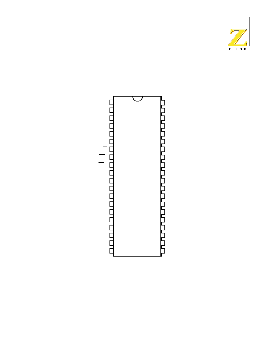
PIN DESCRIPTION
Standard Mode
Figure 2. 40-Pin DIP Pin Configuration
RESET
Z86E61
/E63
1
2
3
4
5
6
7
VCC
XTAL2
P37
P30
R/W
DS
14
10
11
12
13
XTAL1
GND
P32
P00
P01
15
20
16
17
18
19
AS
P35
P02
P03
P06
P07
P05
P04
40
39
38
37
36
35
34
33
32
P36
P31
P21
P27
P26
P25
P24
P23
P22
31
30
29
28
27
P20
P33
P34
P17
P16
26
25
24
23
22
21
P13
P15
P14
P12
P11
P10
8
9
DIP

Z86E61/E63
CMOS Z8 16K/32K EPROM Microcontroller
PS014401-1001
5
Table 17. 40-Pin DIP Pin Identification
Standard Mode
Function
Direction
Pin #
Symbol
1
V
CC
Power Supply
Input
2
XTAL2
Crystal, Oscillator Clock
Output
3
XTAL1
Crystal, Oscillator Clock
Input
4
P37
Port 3, Pin 7
Output
5
P30
Port 3, Pin 0
Input
6
RESET
Reset
Input
7
R/W
Read/Write
Output
8
DS
Data Strobe
Output
9
AS
Address Strobe
Output
10
P35
Port 3, Pin 5
Output
11
GND
Ground
Input
12
P32
Port 3, Pin 2
Input
13-20
P07-P00
Port 0, Pins 0,1,2,3,4,5,6,7
Input/Output
21-28
P17-P10
Port 1, Pins 0,1,2,3,4,5,6,7
Input/Output
29
P34
Port 3, Pin 4
Output
30
P33
Port 3, Pin 3
Input
31-38
P27-P20
Port 2, Pins 0,1,2,3,4,5,6,7
Input/Output
39
P31
Port 3, Pin 1
Input
40
P36
Port 3, Pin 6
Output
Z86E61/E63
CMOS Z8 16K/32K EPROM Microcontroller
PS014401-1001
6
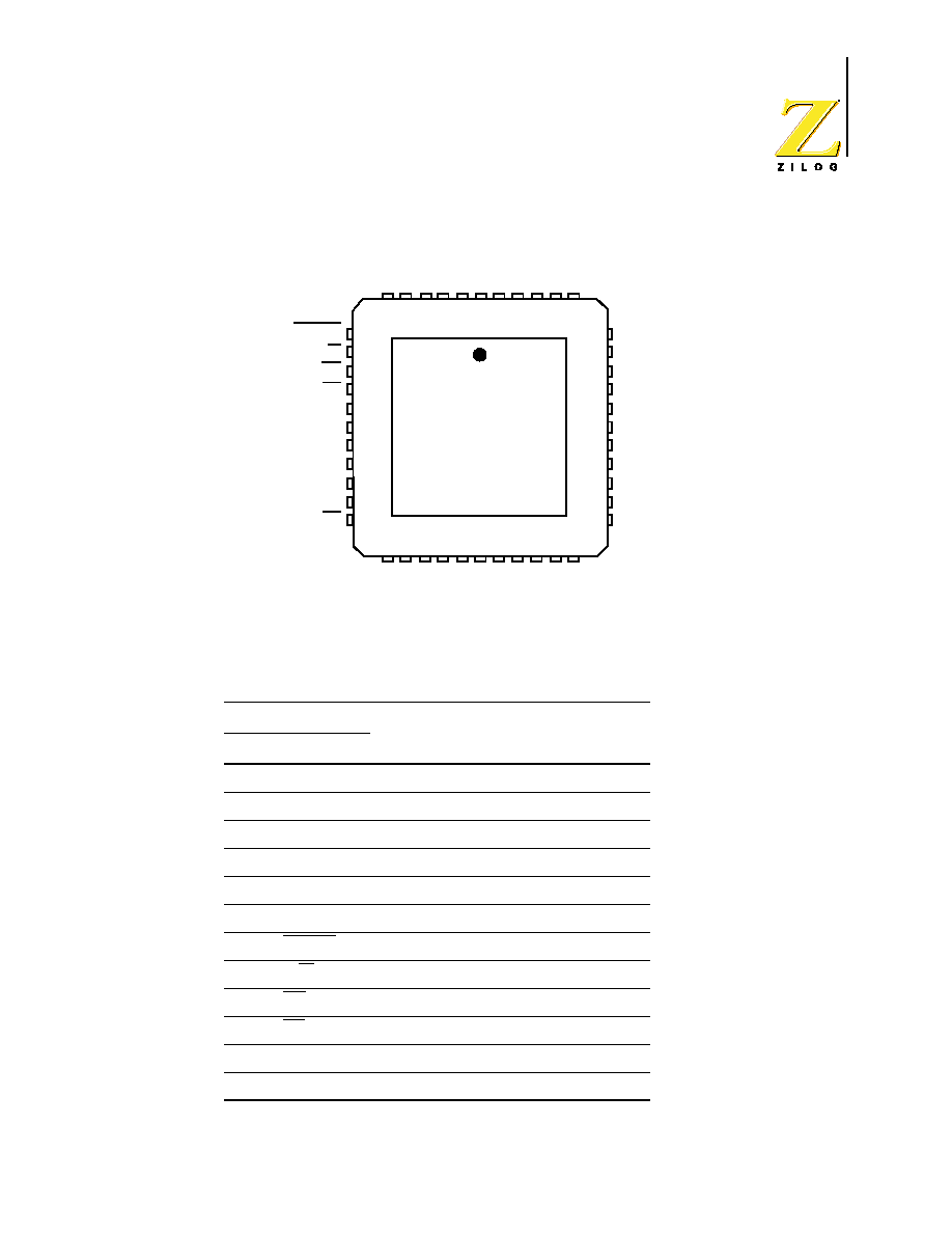
Figure 3. 44-Pin PLCC Pin Configuration
Table 18. 44-Pin PLCC Pin Identification
Standard Mode
Function
Direction
Pin #
Symbol
1
VCC
Power Supply
Input
2
XTAL2
Crystal, Osc. Clock
Output
3
XTAL1
Crystal, Osc. Clock
Input
4
P37
Port 3, Pin 7
Output
5
P30
Port 3, Pin 0
Input
6
N/C
Not Connected
Input
7
RESET
Reset
Input
8
R/W
Read/Write
Output
9
DS
Data Strobe
Output
10
AS
Address Strobe
Output
11
P35
Port 3, Pin 5
Output
12
GND
Ground
Input
GND
AS
DS
R/W
RESET
NC
P24
P23
P21
P22
P20
P33
P34
P17
P16
P15
P35
P32
P00
P01
P02
R/RL
P0
3
P0
6
P0
7
P0
5
P0
4
P1
3
P1
4
P1
2
P1
1
P1
0
NC
P30
NC
P37
XTAL1
XTAL2
VC
C
P36
P31
P27
P26
P25
12
11
10
9
8
7
13
14
15
16
17
6 5 4 3 2 1
40
39
38
37
36
35
34
33
32
31
30
29
41
42
43
44
18 19 20 21 22 23 24 25 26 27 28
Z86E61/E63
PLCC

Z86E61/E63
CMOS Z8 16K/32K EPROM Microcontroller
PS014401-1001
7
13
P32
Port 3, Pin 2
Input
14-16
P02-P00
Port 0, Pins 0, 1,2
Input/Output
17
R/RL
ROM/ROMless control Input
18-22
P 07-P03
Port 0, Pins 3,4,5,6,7
Input/Output
23-27
P 10-P14
Port 1, Pins 0,1,2,3,4
Input/Output
28
N/C
Not Connected
Input
29-31
P17-P15
Port 1, Pins 5,6,7
Input/Output
32
P34
Port 3, Pin 4
Output
33
P33
Port 3, Pin 3
Input
34-38
P24-P20
Port 2, Pins 0,1,2,3,4
Input/Output
39
N/C
Not Connected
Input
40-42
P27-P25
Port 2, Pins 5,6,7
Input/Output
43
P31
Port 3, Pin 1
Input
44
P36
Port 3, Pin 6
Output
Table 18. 44-Pin PLCC Pin Identification (Continued)
Standard Mode
Function
Direction
Pin #
Symbol

Z86E61/E63
CMOS Z8 16K/32K EPROM Microcontroller
PS014401-1001
8
Figure 4. 40-Pin DIP Pin Configuration
Table 19. 40-Pin DIP Pin Identification
EPROM Mode
Function
Direction
Pin #
Symbol
1
V
CC
Power Supply
Input
2
XTAL2
Crystal, Osc. Clock
Output
3
XTAL1
Crystal, Osc. Clock
Input
4
N/C
Not Connected
Input
5
CE
Chip Enable
Input
RESET
Z86E61
/E63
1
2
3
4
5
6
7
VCC
XTAL2
NC
CE
NC
NC
14
10
11
12
13
XTAL1
GND
EPM
A0
A1
15
20
16
17
18
19
NC
NC
A2
A3
A6
A7
A5
A4
40
39
38
37
36
35
34
33
32
NC
OE
A9
PGM
A14
A13
A12
A11
A10
31
30
29
28
27
A8
VPP
NC
D7
D6
26
25
24
23
22
21
D3
D5
D4
D2
D1
D0
8
9
DIP

Z86E61/E63
CMOS Z8 16K/32K EPROM Microcontroller
PS014401-1001
9
Figure 5. 44-Pin PLCC Pin Configuration
6
RESET
Reset
Input
7-10
N/C
Not Connected
Input
11
GND
Ground
Input
12
EPM
EPROM Prog Mode
Input
13-20
A7-A0
Address 0,1,2,3,4,5,6,7
Input
21-28
D7-D0
Data 0,1,2,3,4,5,6,7
In/Output
29
N/C
Not Connected
Input
30
V
PP
Prog Voltage
Input
31-37
A14-A8
Address 8,9,10,11,12,13,14 Input
38
PGM
Prog Mode
Input
39
OE
Output Enable
Input
40
N/C
Not Connected
Input
Table 19. 40-Pin DIP Pin Identification (Continued)
EPROM Mode
Function
Direction
Pin #
Symbol
GND
NC
NC
NC
RESET
A12
A11
A10
A8
A9
VPP
NC
D7
D6
D5
NC
EPM
A0
A1
A2
NC
A3
A6
A7
A5
A4
D3
D4
D2
D1
D0
NC
CE
NC
NC
XT
A
L
1
XT
A
L
2
VC
C
NC
OE
PG
M
A1
4
A1
3
12
11
10
9
8
7
13
14
15
16
17
6 5 4 3 2 1
40
39
38
37
36
35
34
33
32
31
30
29
41
42
43
44
18 19 20 21 22 23 24 25 26 27 28
Z86E61/E63
PLCC
NC

Z86E61/E63
CMOS Z8 16K/32K EPROM Microcontroller
PS014401-1001
10
Table 20. 44-Pin PLCC Pin Identification
EPROM
Pin #
Symbol
Function
Direction
1
V
CC
Power Supply
Input
2
XTAL2
Crystal, Osc. Clock
Input
3
XTAL1
Crystal, Osc. Clock
Input
4
N/C
Not Connected
Input
5
CE
Chip Enable
Input
6
N/C
Not Connected
Input
7
RESET
Reset
Input
8-11
N/C
Not Connected
Input
12
GND
Ground
Input
13
EPM
EPROM Prog Mode
Input
14-16
A0-A2
Address 0,1,2
Input
17
N/C
Not Connected
Input
18-22
A7-A3
Address 3,4,5,6,7
Input
23-27
D4-D0
Data 0,1,2,3,4
In/Output
28
N/C
Not Connected
Input
29-31
D7-D5
Data 5,6,7
In/Output
32
N/C
Not Connected
Input
33
V
PP
Prog Voltage
Input
34-38
A12-A
Address 8,9,10,11,12
Input
39
N/C
Not Connected
Input
40-41
A13-A14
Address 13,14
Input
42
PGM
Prog Mode
Input
43
OE
Output Enable
Input
44
N/C
Not Connected
Input

Z86E61/E63
CMOS Z8 16K/32K EPROM Microcontroller
PS014401-1001
11
PIN FUNCTIONS
ROMless (Input, Active Low).
Connecting this pin to GND disables the internal ROM and forces the device to
function as a Z86C91 ROMless Z8 (see the Z86C91 product specification for
more information). When pulled High to V
CC
, the device functions as a normal
Z86E61/E63 EPROM version.
This pin is only available on the 44-pin versions of the Z86E61/
E63.
DS (Output, Active Low).
Data Strobe is activated once for each external memory transfer. For a READ
operation, data must be available prior to the trailing edge of DS. For WRITE
operations, the falling edge of DS indicates that output data is valid.
AS (Output, Active Low).
Address Strobe is pulsed once at the beginning of each machine cycle. Address
output is through Port 1 for all external programs. Memory address transfers are
valid at the trailing edge of AS. Under program control, AS can be placed in the
high-impedance state along with Ports 0 and 1, Data Strobe, and Read/Write.
XTAL2, XTAL1
Crystal 2, Crystal 1 (time-based input and output, respectively). These pins con-
nect a parallel-resonant crystal, ceramic resonator, LC, or any external single-
phase clock to the on-chip oscillator and buffer.
R/W (Output, Write Low).
The Read/Write signal is Low when the MCU is writing to the external program or
data memory.
RESET (Input, Active Low).
To avoid asynchronous and noisy reset problems, the Z86E61/E63 is equipped
with a reset filter of four external clocks (4TpC). If the external RESET signal is
less than 4TpC in duration, no reset occurs.
Note:

Z86E61/E63
CMOS Z8 16K/32K EPROM Microcontroller
PS014401-1001
12
On the fifth clock after the RESET is detected, an internal RST signal is latched
and held for an internal register count of 18 external clocks, or for the duration of
the external RESET, whichever is longer. During the reset cycle, DS is held active
Low while AS cycles at a rate of TpC/2. When RESET is deactivated, program
execution begins at location 000C (HEX). Power-up reset time must be held low
for 50 ms, or until V
CC
is stable, whichever is longer.
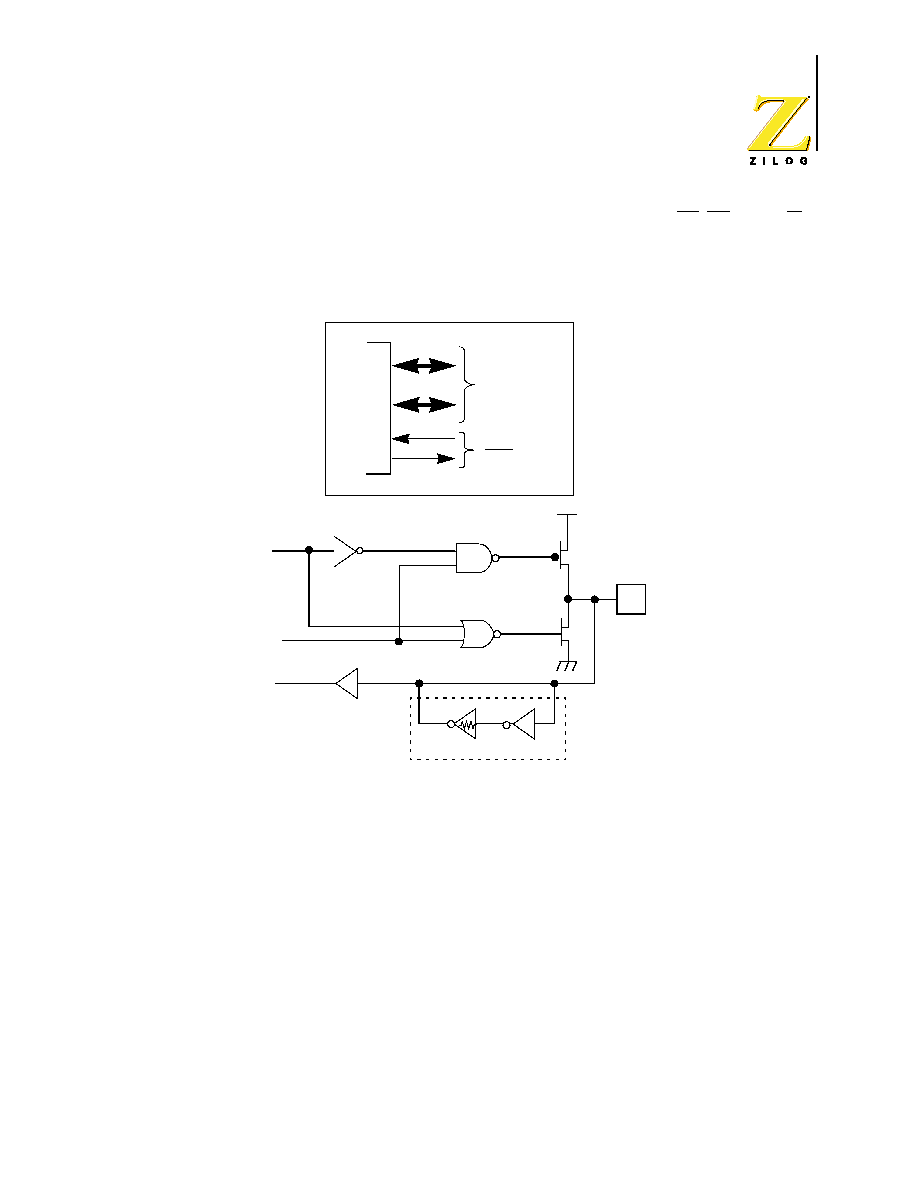
Port 0 (P07-P00)
Port 0 is an 8-bit, nibble programmable, bidirectional, TTL compatible port. These
eight I/O lines can be configured under software control as a nibble I/O port, or as
an address port for interfacing external memory. When used as an I/O port, Port 0
may be placed under handshake control. In this configuration, Port 3, lines P32
and P35 are used as the handshake control DAV0 and RDY0 (Data Available and
Ready). Handshake signal assignment is dictated by the I/O direction of the upper
nibble P07-P04. The lower nibble must have the same direction as the upper nib-
ble to be under handshake control.
For external memory references, Port 0 can provide address bits A11-A8 (lower
nibble) or A15-A8 (lower and upper nibbles) depending on the required address
space. If the address range requires 12 bits or less, the upper nibble of Port 0 can
be programmed independently as I/O while the lower nibble is used for address-
ing. If one or both nibbles are needed for I/O operation, they must be configured
by writing to the Port 0 Mode register.
In ROMless mode, after a hardware reset, Port 0 lines are defined as address
lines A15-A8, and extended timing is set to accommodate slow memory access.
The initialization routine can include reconfiguration to eliminate this extended tim-
ing mode (Figure 8).
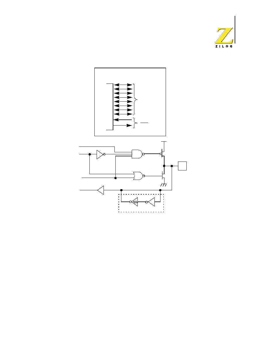
Port 1 (P17-P10)
Port 1 is an 8-bit, byte programmable, bidirectional, TTL compatible port. It has
multiplexed Address (A7-A0) and Data (D7-D0) ports. For Z86E61/E63, these
eight I/O lines can be programmed as input or output lines or are configured under
software control as an address/data port for interfacing external memory. When
used as an I/O port, Port 1 can be placed under handshake control. In this config-
uration, Port 3 lines, P33 and P34, are used as the handshake controls RDY1 and
DAV1.
Memory locations greater than 16384 (E61) or 32768 (E63) are referenced
through Port 1. To interface external memory, Port 1 must be programmed for the
multiplexed Address/ Data mode. If more than 256 external locations are required,
Port 0 must output the additional lines.
Z86E61/E63
CMOS Z8 16K/32K EPROM Microcontroller
PS014401-1001
13
Port 1 can be placed in high-impedance state along with Port 0, AS, DS, and R/W,
allowing the MCU to share common resources in multiprocessor and DMA appli-
cations. Data transfers are controlled by assigning P33 as a Bus Acknowledge
input, and P34 as a Bus Request output (Figure 7).
Figure 6. Port 0 Configuration
Z86E61
/E63
MCU
Port 0 (I/O)
Handshake controls
DAV0 and RDY0
(P32 and P35)
PAD
Auto Latch
R = 500 k
TTL Level Shifter
In
Out
OEN
4
4

Z86E61/E63
CMOS Z8 16K/32K EPROM Microcontroller
PS014401-1001
14
Figure 7. Port 1 Configuration
Port 2 (P27-P20). Port 2 is an 8-bit, bit programmable, bi-directional, CM0S com-
patible port. Each of these eight I/0 lines can be independently programmed as an
input or output, or globally as an open-drain output. Port 2 is always available for I/
0 operation. When used as an I/0 port, Port 2 can be placed under handshake
control. In this configuration, Port 3 lines P31 and P36 are used as the handshake
control lines DAV2 and RDY2. The handshake signal assignment for Port 3 lines,
P31 and P36, is dictated by the direction (input or output) assigned to P27 (Figure
8 and Table 21 on page 16).
Z86E61
/E63
MCU
Port 1
Handshake controls
DAV1 and RDY1
(P33 and P34)
PAD
Auto Latch
R = 500 k
TTL Level Shifter
In
Out
OEN
8
(AD7-AD0)
Z86E61/E63
CMOS Z8 16K/32K EPROM Microcontroller
PS014401-1001
15
Figure 8. Port 2 Configuration
Port 3 (P37-P30). Port 3 is an 8-bit, CMOS compatible four-fixed input and four-
fixed output port. These eight I/O lines have four-fixed (P33-P30) input and four-
fixed (P37-P34) output ports. Port 3, when used as serial I/O, is programmed as
serial in and serial out, respectively (Figure 9).
Z86E61
/E63
MCU
Port 2 (I/O)
Handshake controls
DAV2 and RDY2
(P31 and P36)
PAD
Auto Latch
R = 500 k
TTL Level Shifter
In
Out
OEN
Open-Drain

Z86E61/E63
CMOS Z8 16K/32K EPROM Microcontroller
PS014401-1001
16
Figure 9. Port 3 Configuration
Port 3 is configured under software control to provide the following control func-
tions: handshake for Ports 0 and 2 (DAV and RDY); four external interrupt request
signals (IRQ3-IRQ0); timer input and output signals (TIN and TOUT) Data Mem-
ory Select (/DM) and EPROM control signals (P30 = CE, P31 = OE, P32 = EPM
and P33 = VPP).
1. HS = Handshake Signals D = Data Available R = Ready
Table 21. Port 3 Pin Assignments
Pin
I/O
CTCI
Int.
P0 HS
P1 HS
P2 HS
UART
Ext
EPROM
P30
IN
T
IN
IRQ3
Serial In
CE
P31
IN
T
IN
IRQ2
D/R
OE
P32
IN
T
IN
IRQ0
D/R
EPM
P33
IN
T
IN
IRQ1
D/R
V
PP
P34
OUT
T
OUT
R/D
DM
P35
OUT
T
OUT
R/D
P36
OUT
T
OUT
R/D
P37
OUT
T
OUT
Serial Out
T0
IRQ4
T1
IRQ5
Z86E61
/E63
MCU
Port 3
(I/O or Control)
Z86E61/E63
CMOS Z8 16K/32K EPROM Microcontroller
PS014401-1001
17
UART OPERATION
Port 3 lines, P37 and P30, are programmed as serial I/0 lines for full-duplex serial
asynchronous receiver/transmitter operation. The bit rate is controlled by Counter/
Timer0.
The Z86E61/E63 automatically adds a start bit and two stop bits to transmitted
data (Figure 10). Odd parity is also available as an option. Eight data bits are
always transmitted, regardless of parity selection. If parity is enabled, the eighth
bit is the odd parity bit. An interrupt request (IRQ4) is generated on all transmitted
characters.
Received data must have a start bit, eight data bits, and at least one stop bit. If
parity is on, bit 7 of the received data is replaced by a parity error flag. Received
characters generate the IRQ3 interrupt request.
Figure 10. Serial Data Formats
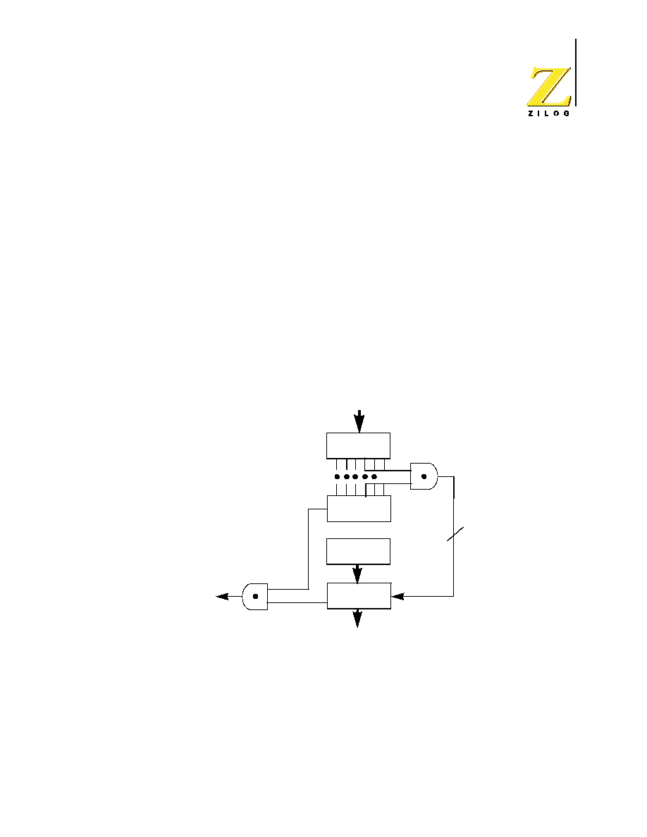
Auto Latch
The Auto Latch puts valid CMOS levels on all CMOS inputs that are not externally
driven. This reduces excessive supply current flow in the input buffer when it is not
driven by any source.
P33-P30 inputs differ from the Z86C61/C63 in that there is no
clamping diode to V
CC
because of the EPROM high voltage
detection circuits. Exceeding the VIH maximum specification
during standard operating mode may cause the device to enter
EPROM mode.
SP
D7 D6 D5 D4 D3 D2 D1 D0 ST
SP
Transmitted Data (No Parity)
Start Bit
Eight Data Bits
Two Stop Bits
SP
P D6 D5 D4 D3 D2 D1 D0 ST
SP
Transmitted Data (With Parity)
Start Bit
Seven Data Bits
Two Stop Bits
Odd Parity
SP D7 D6 D5 D4 D3 D2 D1 D0 ST
Received Data (No Parity)
Start Bit
Eight Data Bits
One Stop Bit
SP P D6 D5 D4 D3 D2 D1 D0 ST
Received Data (With Parity)
Start Bit
One Stop Bit
Parity Error Flag
Note:

Z86E61/E63
CMOS Z8 16K/32K EPROM Microcontroller
PS014401-1001
18
ADDRESS SPACE
Program Memory. The Z86E61/E63 can address 48 Kbytes (E61) or 32 Kbytes
(E63) of external program memory (Figure 11). The first 12 bytes of program
memory are reserved for the interrupt vectors. These locations contain six 16-bit
vectors that correspond to the six available interrupts. For EPROM mode, byte 13
to byte 16383 (E61) or 32767 (E63) consists of on-chip EPROM. At addresses
16384 (E61) or 32768 (E63) and above, the Z86E61/E63 executes external pro-
gram memory fetches. In ROMless mode, the Z86E61/E63 can address up to 64
Kbytes of program memory. Program execution begins at external location 000C
(HEX) after a reset.
Figure 11. Program Memory Configuration
Data Memory (
DM
)
The EPROM version can address up to 48 Kbytes (E61) or 32 Kbytes (E63) of
external data memory space beginning at location 16384 (E61) or 32768 (E63).
The ROMless version can address up to 64 Kbytes of external data memory.
External data memory may be included with, or separated from, the external pro-
gram memory space. DM, an optional I/0 function that can be programmed to
appear on pin P34, is used to distinguish between data and program memory
Interrupt
Vector
(Upper Byte)
Interrupt
Vector
(Lower Byte)
Location of
First Byte of
Instruction
Executed
After RESET
65535
16384 (E61)
32768 (E63)
16383 (E61)
32767 (E63)
12
11
10
9
8
7
6
5
4
3
2
1
0
IRQ5
IRQ5
IRQ4
IRQ4
IRQ3
IRQ3
IRQ2
IRQ2
IRQ1
IRQ1
IRQ0
IRQ0
External
ROM and RAM
On-Chip PROM

Z86E61/E63
CMOS Z8 16K/32K EPROM Microcontroller
PS014401-1001
19
space (Figure 12). The state of the DM signal is controlled by the type instruction
being executed. An LDC opcode references PROGRAM (DM inactive) memory,
and an LDE instruction references DATA (DM active Low) memory.
Register File
The register file consists of four I/0 port registers, 236 general-purpose registers,
and 16 control and status registers (Figure 13). The instructions can access regis-
ters directly or indirectly through an 8-bit address field. The Z86E61/E63 also
allows short 4-bit register addressing using the Register Pointer (Figure 14). In the
4-bit mode, the Register File is divided into 16 working register groups, each occu-
pying 16 continuous locations. The Register Pointer addresses the starting loca-
tion of the active working register group.
Stack
The Z86E61/E63 has a 16-bit Stack Pointer (R255-R254) used for external stacks
that reside anywhere in the data memory for the ROMless mode, but only from
16384 (E61) or 32768 (E63) to 65535 in the EPROM mode. An 8-bit Stack Pointer
(R255) is used for the internal stack that resides within the 236 general-purpose
registers (R239-R4). The high byte of the Stack Pointer (SPH Bits 15-8) can be
use as a general purpose register when using internal stack only.
Z86E61/E63
CMOS Z8 16K/32K EPROM Microcontroller
PS014401-1001
20
Figure 12. Data Memory Configuration
65535
16384 (E61)
32768 (E63)
16383 (E61)
32767 (E63)
0
External
Data
Not Addressable
Memory

Z86E61/E63
CMOS Z8 16K/32K EPROM Microcontroller
PS014401-1001
21
Figure 13. Register File
LOCATION
IDENTIFIERS
R255
R254
R253
R252
R251
R250
R249
R248
R247
R246
R245
R244
R243
R242
R241
R240
R239
R4
R3
R2
R1
R0
General Purpose
Registers
Port 3
Port 2
Port 1
Port 0
Serial I/O
Timer Mode
Timer/Counter1
T1 Prescaler
Timer/Counter0
T0 Prescaler
Port 2 Mode
Port 3 Mode
Port 0-1 Mode
Stack Pointer (Bits 7-0)
Stack Pointer (Bits 15-8)
Register Pointer
Program Control Flags
Interrupt Mask Register
Interrupt Request Register
Interrupt Priority Register
SPL
SPH
RP
FLAGS
IMR
IRQ
IPR
P01M
P3M
P2M
PRE0
T0
PRE1
T1
TMR
SIO
P3
P2
P1
P0

Z86E61/E63
CMOS Z8 16K/32K EPROM Microcontroller
PS014401-1001
22
Figure 14. Register Pointer
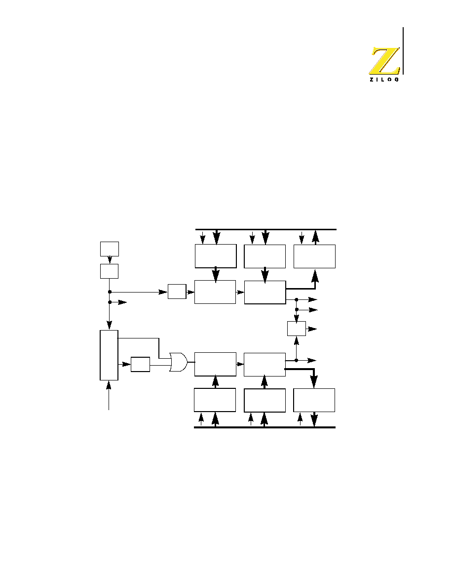
FUNCTIONAL DESCRIPTION
Counter/Timers
There are two 8-bit programmable counter/timers (T0-T1), each driven by its own
6-bit programmable prescaler. The T1 prescaler is driven by internal or external
clock sources; however, the TO prescaler is driven by the internal clock only (Fig-
ure 15).
The 6-bit prescalers can divide the input frequency of the clock source by any
integer number from 1 to 64. Each prescaler drives its counter, which decrements
the value (1 to 256) that has been loaded into the counter. When both the
counters and prescalers reach the end of the count, a timer interrupt request,
IRQ4 (T0) or IRQ5 (T1), is generated.
The counter is programmed to start, stop, restart to continue, or restart from the
initial value. The counters can also be programmed to stop upon reaching zero
R253
r7 r6 r5 r4
r3 r2 r1 r0
(Register Pointer)
The upper nibble of the register file address
provided by the register pointer specifies
the active working-register group.
R15 to R0
The lower nibble of the register file
address provided by the instruction
points to the specified register.
R15 to R0
R15 to R4
R3 to R0
FF
F0
2F
20
1F
10
0F
00
I/O Ports
Register Group 0
Register Group 1
Specified Working
Register Group
Z86E61/E63
CMOS Z8 16K/32K EPROM Microcontroller
PS014401-1001
23
(single pass mode) or to automatically reload the initial value and continue count-
ing (modulo-n continuous mode).
The counter, but not the prescalers, are read at any time without disturbing their
value or count mode. The clock source for T1 is user-definable and is either the
internal microprocessor clock divided-by-four, or an external signal input through
Port 3. The Timer Mode register configures the external timer input (P31) as an
external clock, a trigger input that can be retriggerable or non-retriggerable, or as
a gate input for the internal clock. Port 3 line P36 also serves as a timer output
(TOUT) through which T0, T1, or the internal clock can be output. The counter/
timers are cascaded by connecting the TO output to the input of T1.
Figure 15. Counter/Timers Block Diagram
Interrupts
The Z86E61/E63 has six different interrupts from eight different sources. The
interrupts are maskable and prioritized. The eight sources are divided as follows:
four sources are claimed by Port 3 lines P33-P30, one in Serial Out, one in Serial
In, and two in the counter/timers (Figure 16). The Interrupt Mask Register globally
+4
+4
+2
+2
OSC
Internal
Clock
External Clock
Internal Clock
Gated Clock
Triggered Clock
T
IN
P31
Clock
Logic
Write
Read
Write
Internal Data Bus
T1
Initial Value
Register
PRE1
Initial Value
Register
T1
Current Value
Register
6-Bit
Down
Counter
8-Bit
Down
Counter
6-Bit
Down
Counter
8-Bit
Down
Counter
T0
Initial Value
Register
PRE0
Initial Value
Register
T0
Current Value
Register
Write
Read
Write
Internal Data Bus
IRQ4
Serial I/O
Clock
IRQ5
T
OUT
P36
Z86E61/E63
CMOS Z8 16K/32K EPROM Microcontroller
PS014401-1001
24
or individually enables or disables the six interrupt requests. When more than one
interrupt is pending, priorities are resolved by a programmable priority encoder
that is controlled by the Interrupt Priority register (refer to Table 21 on page 16).
All Z86E61/E63 interrupts are vectored through locations in the program memory.
When an interrupt machine cycle is activated, an interrupt request is granted.
Thus, this disables all of the subsequent interrupts, saves the Program Counter
and Status Flags, and then branches to the program memory vector location
reserved for that interrupt. This memory location and the next byte contain the 16-
bit address of the interrupt service routine for that particular interrupt request.
To accommodate polled interrupt systems, interrupt inputs are masked and the
Interrupt Request register is polled to determine which of the interrupt requests
need service. Software initialized interrupts are supported by setting the appropri-
ate bit in the Interrupt Request Register (IRQ).
Internal interrupt requests are sampled on the falling edge of the last cycle of
every instruction, and the interrupt request must be valid 5TpC before the falling
edge of the last clock cycle of the currently executing instruction.
Figure 16. Interrupt Block Diagram
For the ROMless mode, when the device samples a valid interrupt request, the
next 48 (external) clock cycles are used to prioritize the interrupt, and push the
two PC bytes and the FLAG register on the stack. The following nine cycles are
used to fetch the interrupt vector from external memory. The first byte of the inter-
rupt service routine is fetched beginning on the 58th TpC cycle following the inter-
Global
Interrupt
Enable
IRQ0-IRQ5
IRQ
IMR
IPR
PRIORITY
LOGIC
Vector Select
6
Interrupt
Request

Z86E61/E63
CMOS Z8 16K/32K EPROM Microcontroller
PS014401-1001
25
nal sample point, which corresponds to the 63rd TpC cycle following the external
interrupt sample point.
Clock
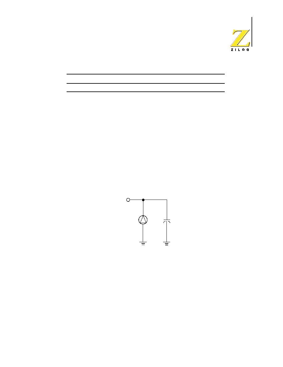
The Z86E61/E63 on-chip oscillator has a high gain, parallel resonant amplifier for
connection to a crystal, LC, ceramic resonator, or any suitable external clock
source (XTAL1 = Input, XTAL2 = Output). The crystal should be AT cut, 1 MHz to
16 MHz max; series resistance (RS) is less than or equal to 100 Ohms. The crys-
tal should be connected across XTAL1 and XTAL2 using the recommended
capacitors (10 pF < CL < 100 pF) from each pin to ground (Figure 17).
Actual capacitor value specified by crystal manufacturer.
Figure 17. Oscillator Configuration
HALT
Turns off the internal CPU clock but not the XTAL oscillation. The counter/timers
and external interrupts IRQ0, IRQ1, IRQ2, and IRQ3 remain active. The devices
are recovered by interrupts, either externally or internally generated. An interrupt
request must be executed (enabled) to exit HALT mode. After the interrupt service
routine, the program continues from the instruction after the HALT.
STOP
This instruction turns off the internal clock and external crystal oscillation, and
reduces the standby current to 5
u
A (typical) or less. The STOP mode is termi-
nated by a reset, which causes the processor to restart the application program at
address
000Ch
.
In order to enter STOP (or HALT) mode, it is necessary to first flush the instruction
pipeline to avoid suspending execution in mid-instruction. To do this, the user
Note:
XTAL1
XTAL2
XTAL1
XTAL2
External Clock
LC Clock
Pin 11
Pin 11
C1
C2
Pin 11
C1
C2
Pin 11
L
Ceramic Resonator
or Crystal
XTAL1
XTAL2

Z86E61/E63
CMOS Z8 16K/32K EPROM Microcontroller
PS014401-1001
26
must execute a NOP (opcode =
0FFH
) immediately before the appropriate SLEEP
instruction. i.e.,
FF
NOP
; clear the pipeline
6F
STOP
; enter STOP mode
or
FF
NOP
; clear the pipeline
7F
HALT
; enter HALT mode
PROGRAMMING
Z86E61/E63 User Modes
The Z86E61/E63 uses separate AC timing cycles for the different User Modes
available. Table 22 on page 27 shows the Z86E61/E63 User Modes. Table 23 on
page 28 shows the timing of the programming waveforms.
User MODE 1 EPROM Read
The Z86E61 /E63 EPROM read cycle is provided so that the user may read the
Z86E61 /E63 as a standard 27128 (E61) or 27256 (E63) EPROM. This is accom-
plished by driving the EPM pin (P32) to VH and activating CE and OE. PGM
remains inactive. This mode is not valid after execution of an EPROM protect
cycle. Timing for the EPROM read cycle is shown in Figure 18.
User MODE 2 EPROM Program
The Z86E61/E63 Program function conforms to the Intelligent programming algo-
rithm. The device is programmed with V
cc
, at 6.0V and V
PP
= 12.5V. Programming
pulses are applied in 1 ms increments to a maximum of 25 pulses before proper
verification. After verification, a programming pulse of three times the duration of
the cycles necessary to program the device is issued to ensure proper program-
ming. After all addresses are programmed, a final data comparison is executed
and the programming cycle is complete. Timing for the Z86E61/E63 programming
cycle is shown in Figure 18.
User Mode 3: PROM Verify
The Program Verify cycle is used as part of the intelligent programming algorithm
to insure data integrity under worst-case conditions. It differs from the EPROM
Read cycle in that Vpp is active and V
CC
must be driven to 6.0V. Timing is shown
in Figure 18.

Z86E61/E63
CMOS Z8 16K/32K EPROM Microcontroller
PS014401-1001
27
User Modes 4 and 5: EPROM and RAM Protect
To extend program security, EPROM and RAM protect cycles are provided for the
Z86E61/E63. Execution of the EPROM protect cycle prohibits proper execution of
the EPROM Read, EPROM Verify, and EPROM programming cycles. Execution
of the RAM protect cycle disables accesses to the upper 128 bytes of register
memory (excluding mode and configuration registers), but first the user's program
must set bit 6 of the IMR (R251). Timing is shown in Figure 20 and Figure 21.
User Modes. Table 6 shows the programming voltage of each mode of the
Z86E61/E63.
Z86E63 Signal Description for EPROM Program/Read
The following signals are required to correctly program or read the Z86E63
device.
ADDR
The address must remain stable throughout the program read cycle.
DATA
The I/O data bus must be stable during programming (OE High, PGM Low, VPP
High). During read the data bus outputs data.
Table 22. OTP Programming
a
a. I
PP
during programming = 40 mA maximum.
I
CC
during programming, verify, or read = 40 mA maximum.
User/Test Mode
Device Pin No.
User Modes
Device Pins
Port 1
CNFG
Data
P33
P32
P30
P31
P20
V
PP
EPM
CE
OE
PGM
ADDR V
CC
EPROM Read
V
IH
V
H
c
c. V
H
= 12.0
±
0.5 V
V
IL
d
d. V
IL
= 0 V
V
IL
V
IH
Addr
5.0V
Out
Program
V
PP
b
b. V
PP
= 12.0
±
0.5 V.
X
V
IL
V
IH
e
e. V
IH
= 5 V.
V
IL
Addr
6.0V
In
Program Verify
V
PP
b
X
V
IL
V
IL
V
IH
Addr
6.0V
Out
EPROM Protect
V
PP
b
V
H
V
H
V
IH
V
IL
XX
f
f.
XX = Irrelevant.
6.0V
XX
RAM Protect
V
PP
X
V
H
V
IH
V
IL
XX
f
6.0V
XX

Z86E61/E63
CMOS Z8 16K/32K EPROM Microcontroller
PS014401-1001
28
XCLK
A clock is required to clock the RESET signal into the registers before program-
ming.
A constant clock can be applied, or the XCLK input can be toggled a minimum of
12 cycles before any programming or verify function begins. The maximum clock
frequency to be applied when in the EPROM mode is 12 MHz.
RESET
The reset input can be held to a constant Low or High value throughout normal
programming. It must be held High to program the EPROM protect option bit.
Also, any time the RESET input changes state the XCLK must be clocked a mini-
mum of 12 times to clock the RESET through the reset filter.
OE
When the device is placed in EPROM mode, the OE input also serves as the pre-
charge for the sense amp. The precharge signal should be Low for the first half of
the stable address and High for the second half. The PRECHG signal is inverted
from the OE signal so the OE should be High on the first half and Low on the sec-
ond half, or stable address. The EPROM output data should be sampled during
the second half of stable address.
The access time of the EPROM is defined in later sections. This two part calcula-
tion of access time is required because this is a precharged sense amp with a pre-
charge clock.
Table 23. Timing of Programming Waveforms
Parameters
Name
Min
Max
Units
1
Address Setup Time
2
µ
s
2
Data Setup Time
2
µ
s
3
V
PP
Setup
2
µ
s
4
V
CC
Setup Time
2
µ
s
5
Chip Enable Setup Time
2
µ
s
6
Program Pulse Width
0.95
ms
7
Data Hold Time
2
µ
s
8
OE Setup Time
2
µ
s
9
Data Access Time
200
ns
10
Data Output Float Time
100
ns
Z86E61/E63
CMOS Z8 16K/32K EPROM Microcontroller
PS014401-1001
29
Figure 18. EPROM Read
11
Over program Pulse Width
2.85
ms
12
EPM Setup Time
2
µ
s
13
PGM Setup Time
2
µ
s
14
Address to OE Setup Time
2
µ
s
15
Option Program Pulse Width
78
ms
Table 23. Timing of Programming Waveforms (Continued)
Parameters
Name
Min
Max
Units
Address
Address Stable
Address Stable
VIH
VIL
VIH
VIL
Data
Invalid
0 Min
Valid
Valid
Invalid
VPP
EPM
VH
VIL
VH
VIL
VIH
VIL
VIH
VIL
VIH
VIL
0 Min
VCC
4.5 V
CE
OE
PGM
5.5 V
12
9
3
Z86E61/E63
CMOS Z8 16K/32K EPROM Microcontroller
PS014401-1001
30
Figure 19. EPROM Program and Verity
Address Stable
Data Stable
Data Out Valid
10
1
2
7
3
4
5
8
9
Program Cycle
Verify Cycle
6
11

Z86E61/E63
CMOS Z8 16K/32K EPROM Microcontroller
PS014401-1001
31
Figure 20. Programming EPROM, RAM Protect, and
4K Size Selection
Address 003
5
Address
VIL
Data
VPP
EPM
VIH
VIL
VCC
CE
OE
PGM
12
ROM Protect
Programming
RAM Protect
Programming
12
15
15
VIH
VIH
VH
VIL
VIH
VH
VIH
VH
6 V
4.5 V
14
3
4
VIH
VH
VIH
VIH
VIL

Z86E61/E63
CMOS Z8 16K/32K EPROM Microcontroller
PS014401-1001
32
Figure 21. Programming EPROM, RAM Protect, and
16K Size Selection
Address 008
5
Address
VIL
Data
VPP
EPM
VIH
VIL
VCC
CE
OE
PGM
12
ROM Protect
Programming
RAM Protect
Programming
12
15
15
VIH
VIH
VH
VIL
VIH
VH
VIH
VH
6 V
4.5 V
14
3
4
VIH
VH
VIH
VIH
VIL

Z86E61/E63
CMOS Z8 16K/32K EPROM Microcontroller
PS014401-1001
33
Figure 22. Intelligent Programming Flowchart
ABSOLUTE MAXIMUM RATINGS
Table 24. Absolute Maximum Ratings
Symbol Description
Min
Max
Units
V
CC
Supply Voltage
a
-0.3
+ 7.0
V
T
STG
Storage Temp
-65
+150
∞C
Device Passed
Device Failed
Start
Verify All
Bytes
Pass
Fail
Verify Byte
Pass
Fail
Fail
Increment
Address
Verify All
Bytes
Fail
Yes
Addr =
First Location
VCC = 6.0 V
VPP = 12.5 V
N = 0
Program
1 ms Pulse
Increment N
N = 25?
No
Pass
Yes
Verify
One Byte
No
Prog. One Pulse
3xN ms Duration
Last Addr?
VCC=VPP=4.5V
VCC=VPP=5.5V
Z86E61/E63
CMOS Z8 16K/32K EPROM Microcontroller
PS014401-1001
34
Stresses greater than those listed under Absolute Maximum Ratings may cause
permanent damage to the device. This is a stress rating only; operation of the
device at any condition above those indicated in the operational sections of these
specifications is not implied. Exposure to absolute maximum rating conditions for
an extended period may affect device reliability.
STANDARD TEST CONDITIONS
The characteristics listed below apply for standard test conditions as noted. All
voltages are referenced to GND. Positive current flows into the referenced pin
(Figure 23).
Figure 23. Test Load Diagram
T
A
Operating Ambient Temperature
Note
b
∞C
a. Voltages on all pins with respect to GND.
b. See See "ORDERING INFORMATION" on page 62.
Table 24. Absolute Maximum Ratings (Continued)
Symbol Description
Min
Max
Units
I
150 pF
From Output
Under Test

Z86E61/E63
CMOS Z8 16K/32K EPROM Microcontroller
PS014401-1001
35
DC CHARACTERISTICS
Table 25. DC Characteristics
Sym
Parameter
T
A
= 0 ∞C to +70∞C
Typical
@ 25 ∞C
Units Conditions
Min
Max
Max Input Voltage
7
V
I
IN
250
µ
A
Max Input Voltage
13
V
P33-P30 Only
V
CH
Clock Input High Voltage 3.8
V
CC
+ 0.3
V
Driven by External Clock Generator
V
CL
Clock Input Low Voltage -0.3
0.8
V
Driven by External Clock Generator
V
IH
Input High Voltage
2.0
V
CC
+ 0.3
V
V
IL
Input Low Voltage
-0.3
0.8
V
V
OH
Output High Voltage
2.4
V
I
OH
= -2.0 mA
V
OL
Output Low Voltage
0.4
V
I
OL
= +2.0 mA
V
RH
Reset Input High Voltage 3.8
V
CC
+ 0.3
V
V
RI
Reset Input Low Voltage -0.3
0.8
V
I
IL
Input Leakage
-10
10
µ
A
0 V V
IN
+ 5.25 V
I
OL
Output Leakage
-10
10
µ
A
0 V V
IN
+ 5.25 V
I
IR
Reset Input Current
-50
µ
A
V
CC
= + 5.25 V, V
RL
= 0 V
I
CC
Supply Current
50
25
mA
@ 16 MHz
60
35
mA
@ 20 MHz
I
CC1
Standby Current
15
5
mA
HALT Mode V
IN
= 0 V, V
CC
@ 16 MHz
20
10
mA
HALT Mode V
IN
= 0 V, V
CC
@ 20 MHz
I
CC2
a
a.
ICC2 requires loading TMR (F1Hh) with any value prior to STOP execution.
Use this sequence:
LD TMR,#00
NOP
STOP
Standby Current
20
5
µ
A
STOP Mode V
IN
= 0 V, V
CC
@ 16 MHz
20
5
µ
A
STOP Mode V
IN
= 0 V, V
CC
@ 20 MHz

Z86E61/E63
CMOS Z8 16K/32K EPROM Microcontroller
PS014401-1001
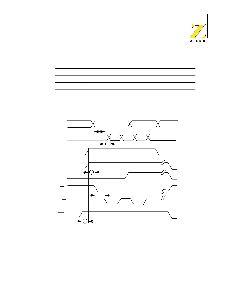
36
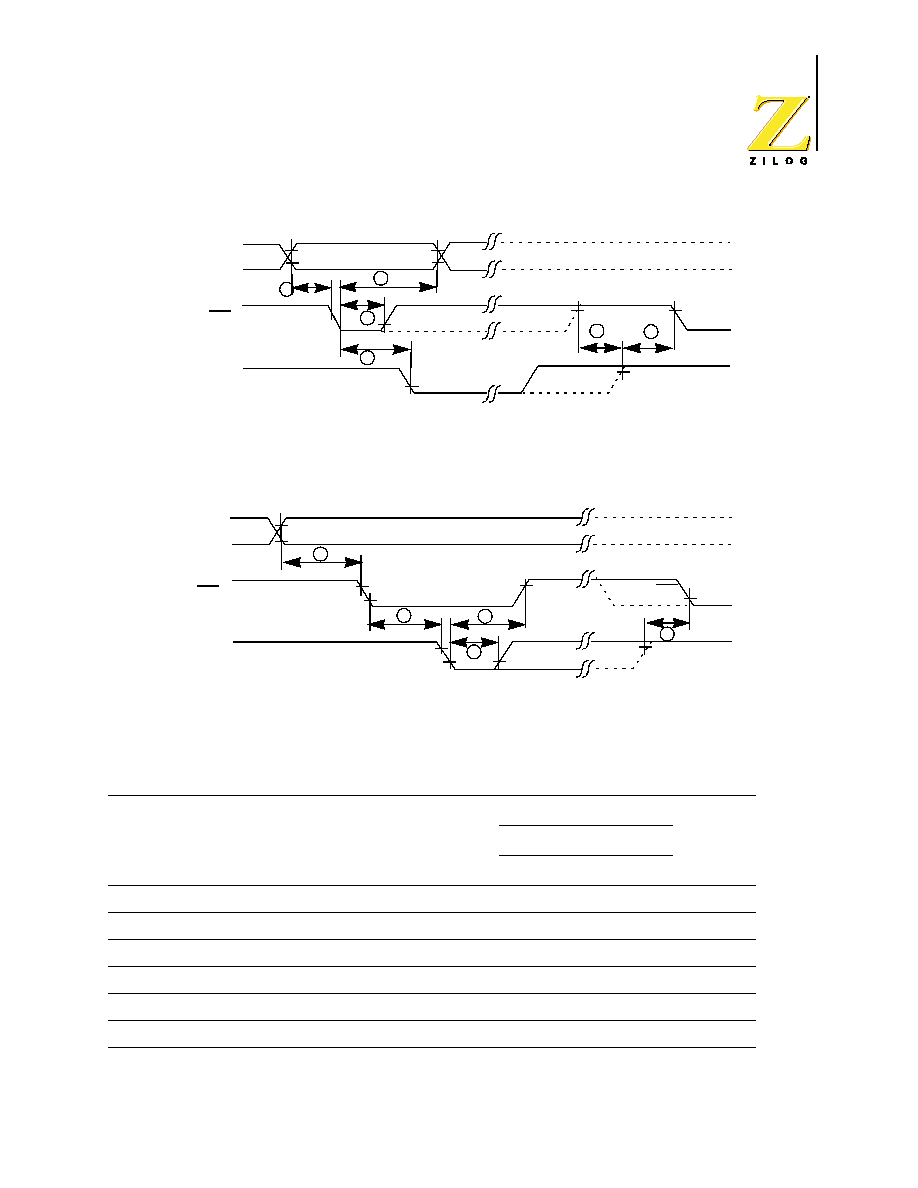
Figure 24. External I/O or Memory Read/Write Timing
9
D7-D0 IN
10
15
11
13
3
16
8
6
7
D7-D0 OUT
14
17
17
2
12
18
1
4
A7-A0
A7-A0
DS
(Write)
Port 1
DS
(Read)
AS
Port 1
Port 0, DM
R/W

Z86E61/E63
CMOS Z8 16K/32K EPROM Microcontroller
PS014401-1001
37
AC CHARACTERISTICS
Table 26. External I/O or Memory Read and Write Timing
No
Symbol
Parameter
TA = 0∞C to +70∞C
Units Notes
16 MHz
a
a. All timing references use 2.0V for a logic 1 and 0.8V for a logic 0.
20 MHz
Min
Max
Min
Max
1
TdA(AS)
Address Valid to AS Rise Delay
20
26
ns
Note
b,c
b. Timing numbers given are for minimum TpC.
c. See Table 11
2
TdAS(A)
AS Rise to Address Float Delay
30
28
ns
Note
b,c
3
TdAS(DR)
AS Rise to Read Data Req'd Valid
180
160
ns
Note
b,c,d
d. When using extended memory timing add 2 TpC.
4
TwAS
AS Low Width
35
36
ns
Note
b,c
5
TdAZ(DS)
Address Float to DS Fall
0
0
ns
6
TwDSR
DS (Read) Low Width
135
130
ns
Note
b,c,d
7
TwDSW
DS (Write) Low Width
80
75
ns
Note
b,c,d
8
TdDSR(DR)
DS Fall to Read Data Req'd Valid
75
100
ns
Note
b,c,d
9
ThDR(DS)
Read Data to DS Rise Hold Time 0
0
ns
Note
b,c
10
TdDS(A)
DS Rise to Address Active Delay
35
48
ns
Note
b,c
11
TdDS(AS)
DS Rise to AS Fall Delay
30
36
ns
Note
b,c
12
TdR/W(AS)
R/W Valid to AS Rise Delay
20
32
ns
Note
b,c
13
TdDS(R/W)
DS Rise to R//W Not Valid
30
36
ns
Note
b,c
14
TdDW(DSW)
Write Data Valid to DS Fall (Write)
Delay
25
40
ns
Note
b,c
15
TdDS(DW)
DS Rise to Write Data Not Valid
Delay
30
40
ns
Note
b,c
16
TdA(DR)
Address Valid to Read Data Req'd
Valid
200
200
ns
Note
b,c,d
17
TdAS(DS)AS
AS Rise to DS Fall Delay
40
48
ns
Note
b,c
18
TdDM(AS)
DM Valid to AS Fall Delay
30
36
ns
Note
b,c

Z86E61/E63
CMOS Z8 16K/32K EPROM Microcontroller
PS014401-1001
38
Table 27. Clock Dependent Formulas
Number Symbol
Equation
1
TdA(AS)
0.40 TpC + 0.32
2
TdAS(A)
0.59 TpC - 3.25
3
TdAS(DR)
2.83 TpC + 6.14
4
TwAS
0.66 TpC - 1.65
6
TwDSR
2.33 TpC - 10.56
7
TwDSW
1.27 TpC + 1.67
8
TdDSR(DR)
1.97 TpC - 42.5
10
TdDS(A)
0.8 TpC
11
TdDS(AS)
0.59 TpC - 3.14
12
TdR/W(AS)
0.4 TpC
13
TdDS(R/W)
0.8 TpC - 15
14
TdDW(DSW)
0.4 sTpC
15
TdDS(DW)
0.88 TpC - 19
16
TdA(DR)
4 TpC - 20
17
TdAS(DS)
0.91 TpC - 10.7
18
TdDM(AS)
0.9 TpC - 26.3
Z86E61/E63
CMOS Z8 16K/32K EPROM Microcontroller
PS014401-1001
39
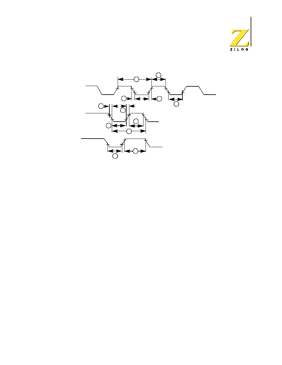
Figure 25. Additional Timing
8
Clock
TIN
IRQN
9
6
5
4
7
2
2
3
3
1
7

Z86E61/E63
CMOS Z8 16K/32K EPROM Microcontroller
PS014401-1001
40
AC CHARACTERISTICS
Table 28. Additional Timing
No
Symbol
Parameter
TA = 0∞C to +70∞C
Units Notes
16 MHz
20 MHz
Min
Max
Min
Max
1
TpC
Input Clock Period
62.5
1000 50
1000 ns
Note
a
a. Clock timing references use 3.8V for a logic 1 and 0.8V for a logic 0.
2
TrC,TfC
Clock Input Rise & Fall Times
10
15
ns
Note
a
3
TwC
Input Clock Width
21
37
ns
Note
a
4
TwTinL
Timer Input Low Width
50
75
ns
Note
b
b. Timing references use 2.0V for a logic 1 and 0.8V for a logic 0.
5
TwTinH
Timer Input High Width
5TpC
5TpC
Note
b
6
TpTin
Timer Input Period
8TpC
8TpC
Note
b
7
TrTin,TfTin
Timer Input Rise & Fall Times
100
100
ns
Note
b
8A
TwIL
Interrupt Request Input Low Times 70
50
ns
Note
b,c
c. Interrupt request through Port 3 (P33-P31).
8B
TwIL
Interrupt Request Input Low Times 5TpC
5TpC
Note
b,d
d. Interrupt request through Port 30.
9
TwIH
Interrupt Request Input High Times 5TpC
5TpC
Note
b,e
e. Interrupt references request through Port 3.
Z86E61/E63
CMOS Z8 16K/32K EPROM Microcontroller
PS014401-1001
41
Figure 26. Input Handshake Timing
Figure 27. Output Handshake Timing
Table 29. Handshake Timing
No
Symbol
Parameter
T
A
= 0∞C to +70∞C
Data
Direction
16 MHz
20 MHz
Min
Max
Min
Max
1
TsDI(DAV)
Data In Setup Time
0
0
IN
2
ThDI(DAV)
Data In Hold Time
145
145
IN
3
TwDAV
Data Available Width
110
110
IN
4
TdDAVI(RDY)
DAV Fall to RDY Fall Delay
115
115
IN
5
TdDAVId(RDY)
DAV Rise to RDY Rise Delay
115
115
IN
6
TdRDY0(DAV)
RDY Rise to DAV Fall Delay
0
0
IN
7
TdD0(DAV)
Data Out to DAV Fall Delay
TpC
TpC
OUT
Delayed DAV
Next Data In Valid
Delayed RDY
Data In Valid
RDY
(Output)
DAV
(Input)
Data In
5
6
4
1
2
3
Next Data Out Valid
Data Out Valid
Delayed DAV
Delayed RDY
RDY
(Input)
DAV
Data Out
(Output)
11
10
9
8
7
Z86E61/E63
CMOS Z8 16K/32K EPROM Microcontroller
PS014401-1001
42
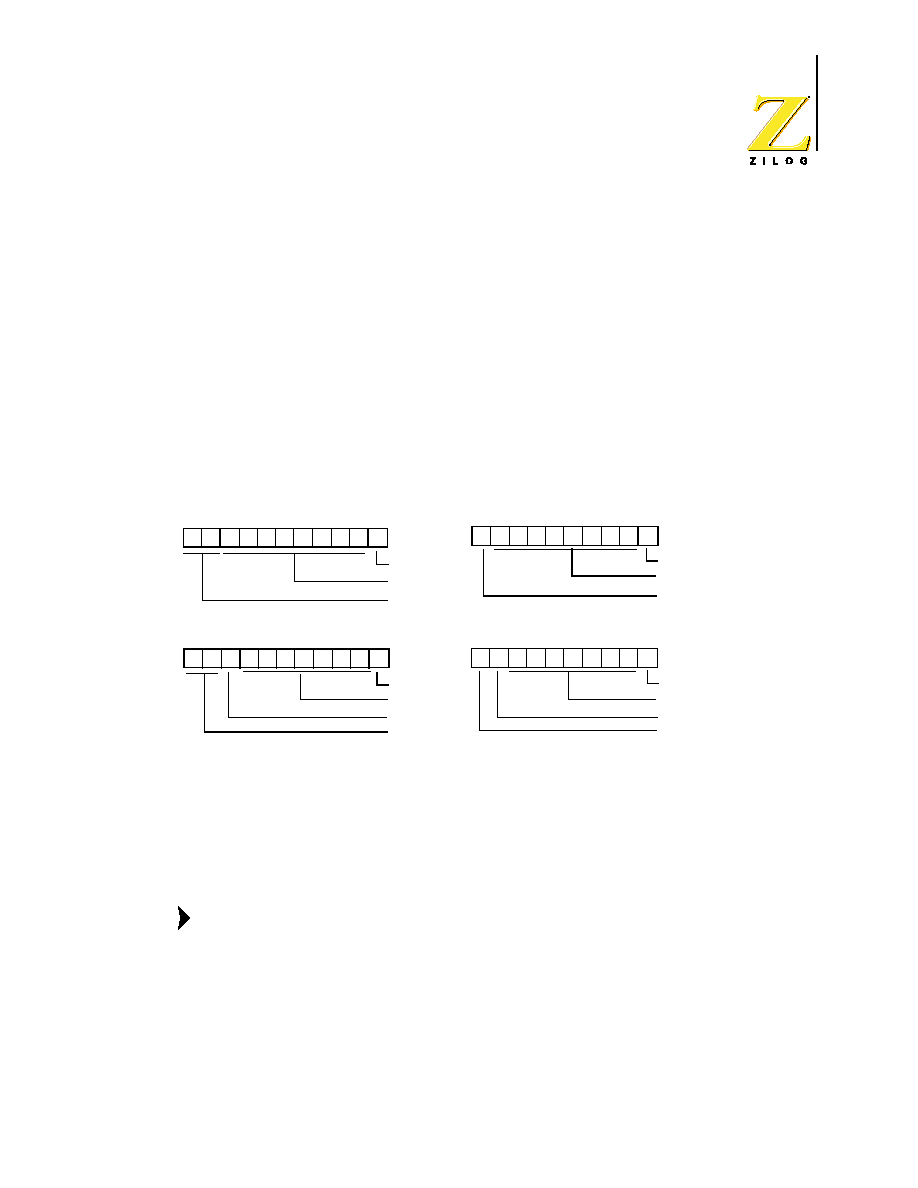
Z8 CONTROL REGISTER DIAGRAMS
Figure 28. Serial I/O Register (F0
H
: Read/Write)
8
TdDAV0(RDY)
DAV Fall to RDY Fall Delay
0
0
OUT
9
TdRDY0(DAV)
RDY Fall to DAV Rise Delay
115
115
OUT
10
TwRDY
RDY Width
110
110
OUT
11
TdRDY0d(DAV)
RDY Rise to DAV Fall Delay
115
115
OUT
Table 29. Handshake Timing (Continued)
No
Symbol
Parameter
T
A
= 0∞C to +70∞C
Data
Direction
16 MHz
20 MHz
Min
Max
Min
Max
R240 SIO
D7
D6
D5
D4
D3
D2
D1
D0
Serial Data (D0 = LSB)

Z86E61/E63
CMOS Z8 16K/32K EPROM Microcontroller
PS014401-1001
43
Figure 29. Timer Mode Register (F1
H
: Read/Write)
Figure 30. Counter/Timer 1 Register (F2
H
: Read/Write)
R241 TMR
D7
D6
D5
D4
D3
D2
D1
D0
0 No Function
1 Load T0
0 Disable T0 Count
1 Enable T0 Count
0 No Function
1 Load T1
0 Disable T1 Count
1 Enable T1 Count
T
IN
Modes
00 External Clock Input
01 Gate Input
10 Trigger Input
(Non-retriggerable)
11 Trigger Input
(Regriggerable)
T
OUT
Modes
00 Not Used
01 T0 Out
10 T1 Out
11 Internal Clock Out
R242 T1
D7
D6
D5
D4
D3
D2
D1
D0
T1 Intial Value
(When Written)
(Range: 1-256 Decimal
01-00 HEX)
T1 Current Value
(When Read)

Z86E61/E63
CMOS Z8 16K/32K EPROM Microcontroller
PS014401-1001
44
Figure 31. Prescaler 1 Register (F3
H
: Write Only)
Figure 32. Counter/Timer 0 Register (F4
H
: Read/Write)
Figure 33. Prescaler 0 Register (F5
H
: Write Only)
R243 PRE1
D7
D6
D5
D4
D3
D2
D1
D0
Count Mode
0 T1 Single Pass
1 T1 Modulo N
Clock Source
1 T1 Internal
0 T1 External Timing Input
(T
IN
) Mode
Prescaler Modulo
(Range: 1-64 Decimal
01-00 HEX)
R244 T0
D7
D6
D5
D4
D3
D2
D1
D0
T0 Initial Value
(When Written)
(Range: 1-256 Decimal
01-00 HEX)
T0 Current Value
(When Read)
R245 PRE0
D7
D6
D5
D4
D3
D2
D1
D0
Count Mode
0 T0 Single Pass
1 T0 Modulo N
Reserved (Must be 0)
Prescaler Modulo
(Range: 1-64 Decimal
01-00 HEX)

Z86E61/E63
CMOS Z8 16K/32K EPROM Microcontroller
PS014401-1001
45
Figure 34. Port 2 Mode Register (F6
H
: Write Only)
Figure 35. Port 3 Mode Register (F7
H
: Write Only)
R246 P2M
D7
D6
D5
D4
D3
D2
D1
D0
P20 - P27 I/O Definition
0 Defines Bit as Output
1 Defines Bit as Input
R247 P3M
D7
D6
D5
D4
D3
D2
D1
D0
0 Port 2 Pull-Ups Open Drain
1 Port 3 Pull-Ups Active
Reserved (Must be 0)
0 P32 - Input
P35 = Output
1 P32 = DAV0/RDY0
P35 = RDY0/DAV0
00 P33 = Input
P34 = Output
01 P33 = Input
10 P34 = DM
11 P33 = DAV1/RDY1
P34 = RDY1/DAV1
0 P31 = Input (TIN)
P36 = Output (TOUT)
1 P31 = DAV2/RDY2
P36 = RDY2/DAV2
0 P30 = Input
P37 = Output
1 P30 = Serial In
P37 = Serial Out
0 Parity Off
1 Parity On
Z86E61/E63
CMOS Z8 16K/32K EPROM Microcontroller
PS014401-1001
46
Figure 36. Port 0 and 1 Mode Register (F8
H
: Write Only)
R248 P01M
D7
D6
D5
D4
D3
D2
D1
D0
PO0 - PO0 Mode
00 Output
01 Input
1X A11-A8
Stack Selection
0 External
1 Internal
P17 - P10 Mode
00 Byte Output
01 Byte Input
10 AD7 - AD0
11 High-Impedance AD7 - DA0,
AS, DS, R/W, A11-A8
A15- A12, If Selected
External Memory Timing
0 Normal
1 Extended
P07 - P04 Mode
00 Output
01 Input
1X A15 - A12
Z86E61/E63
CMOS Z8 16K/32K EPROM Microcontroller
PS014401-1001
47
Figure 37. Interrupt Priority Register (F9
H
: Write Only)
Figure 38. Interrupt Request Register (FA
H
: Read/Write)
R249 IPR
D7
D6
D5
D4
D3
D2
D1
D0
Interrupt Group Priority
Reserved = 00
C > A > B = 001
A > B > C = 010
A > C > B = 011
B > C > A = 100
C > B > A = 101
B > A > C = 110
Reserved = 111
IRQ1, IRQ4 Priority (Group C)
0 IRQ1 > IRQ4
1 IRQ4 > IRQ1
IRQ0, IRQ2 Priority (Group B)
0 IRQ2 > IRQ0
1 IRQ0 > IRQ2
IRQ3, IRQ5 Priority (Group A)
0 IRQ5 > IRQ3
1 IRQ3 > IRQ5
Reserved (Must be 0)
R250 IRQ
D7
D6
D5
D4
D3
D2
D1
D0
IRQ0 = P32 Input (D0 = IRQ0)
IRQ1 = P33 Input
IRQ2 = P31 Input
IRQ3 = P30 Input, Serial Input
IRQ4 = T0 Serial Output
IRQ5 = T1
Reseserved (Must be 0)
Z86E61/E63
CMOS Z8 16K/32K EPROM Microcontroller
PS014401-1001
48
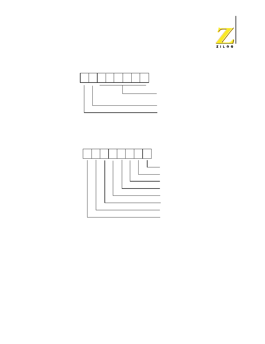
Figure 39. Interrupt Mask Register (FB
H
: Read/Write)
Figure 40. Flag Register (FC
H
: Read/Write)
R251 IMR
D7
D6
D5
D4
D3
D2
D1
D0
1 Enables IRQ5-IRQ0
(D0 = IRQ0)
1 Enables RAM Protect
1 Enables Interrupts
R252 SPL FLAGS
D7
D6
D5
D4
D3
D2
D1
D0
User Flag F1
User Flag F2
Half Carry Flag
Decimal Adjust Flag
Overflow Flag
Sign Flag
Zero Flag
Carry Flag

Z86E61/E63
CMOS Z8 16K/32K EPROM Microcontroller
PS014401-1001
49
Figure 41. Register Pointer Register (FD
H
: Read/Write)
Figure 42. Stack Pointer Register (FE
H
: Read/Write)
Figure 43. Stack Pointer Register (FF
H
: Read/Write)
R253 SPL
D7
D6
D5
D4
D3
D2
D1
D0
Reserved (Must be 0)
Register Pointer
0
f4
r5
r6
r7
R254 SPL
D7
D6
D5
D4
D3
D2
D1
D0
Stack Pointer Lower
Byte (SP15 - SP8)
R255 SPL
D7
D6
D5
D4
D3
D2
D1
D0
Stack Pointer Lower
Byte (SP7 - SP0)

Z86E61/E63
CMOS Z8 16K/32K EPROM Microcontroller
PS014401-1001
50
DC CHARACTERISTICS
Supply Current
Figure 44. Typical I
CC
vs. Frequency
40
30
20
10
0
2
4
6
8
10
12
14 16
18
20
Frequency (MHz)
I
CC
(mA)
Legend:
A ≠ Vcc = 5.6V
C ≠ VCc = 4.4V
A
B
C
B ≠ Vcc = 5.0V
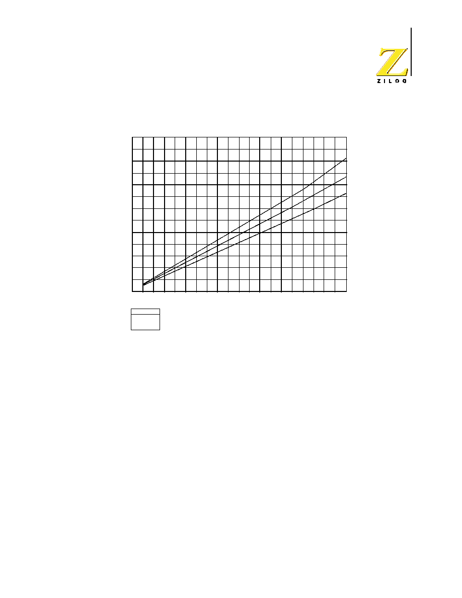
Z86E61/E63
CMOS Z8 16K/32K EPROM Microcontroller
PS014401-1001
51
Standby Current
Figure 45. Typical I
CC1
vs. Frequency
12
10
8
6
4
2
I
CC1
(mA)
0
2
4
6
8
10
12
14
16
18 20
Frequency (MHz)
Legend:
A ≠ Vcc = 5.6V
C ≠ VCc = 4.4V
B ≠ Vcc = 5.0V
A
B
C

Z86E61/E63
CMOS Z8 16K/32K EPROM Microcontroller
PS014401-1001
52
INSTRUCTION SET NOTATION
Addressing Modes. The following notation is used to describe the addressing
modes and instruction operations as shown in the instruction summary (Table 14).
Symbols. The following symbols are used in describing the instruction set.
Table 30. Instruction Set Notation
Symbol Meaning
IRR
Indirect register pair or indirect working register pair
address
Irr
Indirect working register pair only
X
Indexed address
DA
Direct address
RA
Relative address
IM
Immediate
R
Register or working register address
r
Working register address only
IR
Indirect register or indirect working register address
Ir
Indirect working register address only
RR
Register pair or working register pair address
Symbol Meaning
dst
Destination location or contents
src
Source location or contents
cc
Condition Code
@
Indirect address prefix
SP
Stack Pointer
PC
Program Counter
FLAGS
Flag Register (Control Register 252)
RP
Register Pointer (R253)
IMR
Interrupt Mask Register (R251)

Z86E61/E63
CMOS Z8 16K/32K EPROM Microcontroller
PS014401-1001
53
Flags. Control register (R252) contains the following six flags:
Affected flags are indicated by:
CONDITION CODES
Symbol Meaning
C
Carry flag
Z
Zero flag
S
Sign flag
V
Overflow flag
D
Decimal-adjust flag
H
Half-carry flag
Symbol Meaning
0
Clear to zero
1
Set to one
*
Set to clear according to
operation
-
Unaffected
x
Undefined
Table 31. Condition Codes
Value
Mnemonic Meaning
Flags Set
1000
Always True
0111
C
Carry
C = 1
1111
NC
No Carry
C = 0
0110
Z
Zero
Z = 1
1110
NZ
Not Zero
Z = 0
1101
PL
Plus
S = 0
0101
MI
Minus
S = 1
0100
OV
Overflow
V = 1
1100
NOV
No Overflow
V = 0
0110
EQ
Equal
Z = 1
1110
NE
Not Equal
Z = 0
1001
GE
Greater Than or Equal
(S XOR V) = 0

Z86E61/E63
CMOS Z8 16K/32K EPROM Microcontroller
PS014401-1001
54
0001
LT
Less than
(S XOR V) = 1
1010
GT
Greater Than
[Z OR (S XOR V)] = 0
0010
LE
Less Than or Equal
[Z OR (S XOR V)] = 1
1111
UGE
Unsigned Greater Than or
Equal
C = 0
0111
ULT
Unsigned Less Than
C = 1
1011
UGT
Unsigned Greater Than
(C = 0 AND Z = 0) = 1
0011
ULE
Unsigned Less Than or Equal
(C OR Z) = 1
0000
F
Never True (Always False)
Table 31. Condition Codes (Continued)
Value
Mnemonic Meaning
Flags Set

Z86E61/E63
CMOS Z8 16K/32K EPROM Microcontroller
PS014401-1001
55
INSTRUCTION FORMATS
Figure 46. Instruction Formats
CCF, DI, EI, IRET, NOP,
RCF, RET, SCF
One-Byte Instructions
CLR, CPL, DA, DEC,
DECW, INC, INCW,
POP, PUSH, RL, RLC,
RR, RRC, SRA, SWAP
JP, CALL (Indirect)
SRP
ADC, ADD, AND, CP,
OR, SBC, SUB, TCM,
TM, XOR
LD, LDE, LDEI,
LDC, LDCI
LD
LD
DJNZ, JR
STOP/HALT
Two-Byte Instructions
Three-Byte Instructions
OPC
MODE
dst/src
OPC
dst
OPC
VALUE
src
dst
dst/src
src/dst
src/dst
dst/src
OPC
OPC
OPC
OPC
OPC
MODE
MODE
dst
MODE
VALUE
dst/CC
RA
FFH
6FH
7FH
OR
OR
OR
OR
OR
OR
OR
OR
1 1 1 0
1 1 1 0
1 1 1 0
1 1 1 0
1 1 1 0
1 1 1 0
1 1 1 0
1 1 1 0
OPC
OPC
OPC
OPC
OPC
OPC
MODE
MODE
MODE
dst
dst
dst
src
src
dst/src
X
ADDRESS
CC
DAU
DAL
DAU
DAL
LD
LD
JP
CALL
dst/src
dst
dst
dst
dst
src
src
ADC, ADD, AND, CP
LD, OR, SBC, SUB,
TCM, TM, XOR
ADC, ADD, AND, CP
LD, OR, SBC, SUB,
TCM, TM, XOR
VALUE
src
OPC
OPC
dst

Z86E61/E63
CMOS Z8 16K/32K EPROM Microcontroller
PS014401-1001
56
INSTRUCTION SUMMARY
Note: Assignment of a value is indicated by the symbol "
". For example:
dst
dst + src
indicates that the source data is added to the destination data and the result is
stored in the destination location. The notation "addr (n)" is used to refer to bit (n)
of a given operand location. For example:
dst (7)
refers to bit 7 of the destination operand
Table 32. Instruction Summary
Instruction
and Operation
Address Mode
Opcode
Byte (Hex)
Flags Affected
dst
src
C
Z
S
V
D
H
ADC dst, src
Note
a
1[ ]
*
*
*
*
0
*
dst
dst + src +C
ADD dst, src
Note
a
0[ ]
*
*
*
*
0
*
dst
dst + src
AND dst, src
Note
a
5[ ]
-
*
*
0
-
-
dst
dst AND src
CALL dst
DA
06
-
-
-
-
-
-
SP
SP-2
IRR
D4
@SP
PC,
PC
dst
CCF
EF
*
-
-
-
-
-
C
NOT C
CLR dst
R
B0
-
-
-
-
-
-
dst
0
IR
B11
COM dst
R
60
-
*
*
0
-
-
dst
NOT dst
IR
61
CP dst, src
Note
a
A[ ]
*
*
*
*
-
-
dst - src
DA dst
R
40
*
*
*
X
-
-
dst
DA dst
IR
41

Z86E61/E63
CMOS Z8 16K/32K EPROM Microcontroller
PS014401-1001
57
DEC dst
R
00
-
*
*
*
-
-
dst
dst -1
IR
01
DECW dst
RR
80
-
*
*
*
-
-
dst
dst-1
IR
81
DI
8F
-
-
-
-
-
-
IMR(7)
0
DJNZr, dst
RA
rA
-
-
-
-
-
-
r
r -1
r = 0-F
if r
0
PC
PC + dst
Range: +127,
-128
EI
9F
-
-
-
-
-
-
IMR(7)
1
HALT
7F
-
-
-
-
-
-
INC dst
r
rE
-
*
*
*
-
-
dst
dst + 1
r = 0 - F
R
20
IR
21
INCW dst
RR
A0
-
*
*
*
-
-
dst
dst + 1
IR
A1
IRET
BF
*
*
*
*
*
*
FLAGS
@SP;
SP
SP + 1
PC
@SP;
SP
SP + 2;
IMR(7)
1
JP cc, dst
DA
cD
-
-
-
-
-
-
Table 32. Instruction Summary (Continued)
Instruction
and Operation
Address Mode
Opcode
Byte (Hex)
Flags Affected
dst
src
C
Z
S
V
D
H

Z86E61/E63
CMOS Z8 16K/32K EPROM Microcontroller
PS014401-1001
58
if cc is true,
c = 0 - F
PC
dst
IRR
30
JR cc, dst
RA
cB
-
-
-
-
-
-
if cc is true,
c = 0 - F
PC
PC + dst
Range: +127,
-128
LD dst, src
r
Im
rC
-
-
-
-
-
-
dst
src
r
R
r8
R
r
r9
r = 0-F
r
X
C7
X
r
D7
r
Ir
E3
Ir
r
F3
R
R
E4
R
IR
E5
R
IM
E6
IR
IM
E7
IR
R
F5
LDC dst, src
r
Irr
C2
-
-
-
-
-
-
dst
src
LDCI dst, src
Ir
Irr
C3
-
-
-
-
-
-
dst
src
r
r + 1;
rr
rr + 1
NOP
FF
-
-
-
-
-
-
OR dst, src
Note
a
4[ 1
-
*
*
0
-
-
Table 32. Instruction Summary (Continued)
Instruction
and Operation
Address Mode
Opcode
Byte (Hex)
Flags Affected
dst
src
C
Z
S
V
D
H

Z86E61/E63
CMOS Z8 16K/32K EPROM Microcontroller
PS014401-1001
59
dst
dst OR src
POP
R
50
-
-
-
-
-
-
dst
@SP;
IR
51
SP
SP + 1
PUSH src
R
70
-
-
-
-
-
-
SP
SP-1;
IR
71
@SP
src
RCF
CF
0
-
-
-
-
-
C
0
RET
AF
-
-
-
-
-
-
PC
@SP;
SP
SP +2
RL dst
R
90
*
*
*
*
-
-
IR
91
RLC dst
R
10
*
*
*
*
-
-
IR
11
RR dst
R
E0
*
*
*
*
-
-
IR E1
RRC dst
R
C0
*
*
*
*
-
-
IR
C1
SBC dst, src
Note
a
3[ ]
*
*
*
*
1
*
dst
dst
src
C
SCF
DF
1
-
-
-
-
-
C
1
SRA dst
R
D0
*
*
*
0
-
-
IR
D1
SRP dst
Im
31
-
-
-
-
-
-
Table 32. Instruction Summary (Continued)
Instruction
and Operation
Address Mode
Opcode
Byte (Hex)
Flags Affected
dst
src
C
Z
S
V
D
H
c
7
0
c
7
0
c
7
0
c
7
0
c
7
0

Z86E61/E63
CMOS Z8 16K/32K EPROM Microcontroller
PS014401-1001
60
RP
src
STOP
6F
1
-
-
-
-
-
SUB dst, src
Note
a
2[ ]
[
[
[
[
1
[
dst
dst
src
SWAP dst
R
F0
X
*
*
X
-
-
IR
F1
TCM dst, src
Note
a
6[ ]
-
*
*
0
-
-
(NOT dst)
AND src
TM dst, src
Note
a
7[ ]
-
*
*
0
-
-
dst AND src
XOR dst, src
Note
a
B[ ]
-
*
*
0
-
-
dst
dst
XOR src
a.
These instructions have an identical set of addressing modes, which are encoded for brevity. The first Op
Code nibble is found in the instruction set table above. The second nibble is expressed symbolically by a
'[ ]' in this table, and its value is found in the following table to the left of the applicable addressing mode pair.
For example, the opcode of an ADC instruction using the addressing modes r (destination) and Ir (source)
is 13.
Address Mode
Lower
Opcode Nibble
dst
src
r
r
[2]
r
Ir
[3]
R
R
[4]
R
IR
[5]
R
IM
[6]
IR
IM
[7]
Table 32. Instruction Summary (Continued)
Instruction
and Operation
Address Mode
Opcode
Byte (Hex)
Flags Affected
dst
src
C
Z
S
V
D
H
7
0
7
0
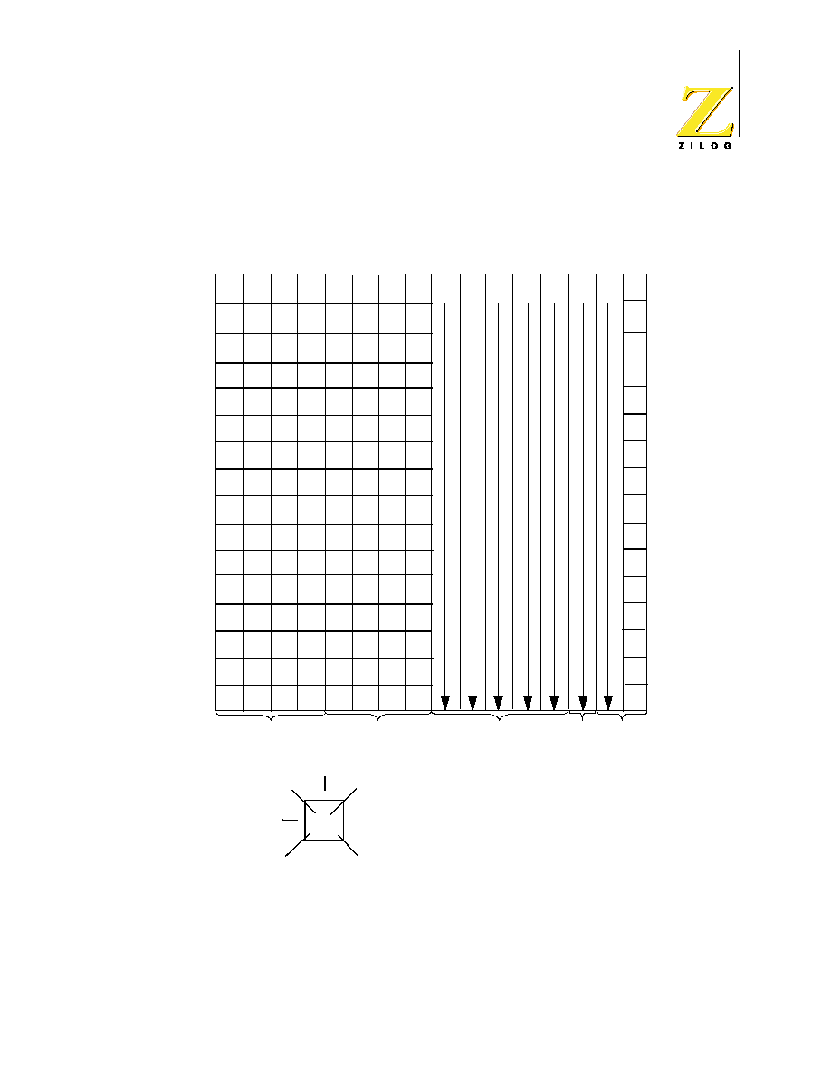
Z86E61/E63
CMOS Z8 16K/32K EPROM Microcontroller
PS014401-1001
61
OPCODE MAP
Figure 47. Opcode Map
0
0
1
2
3
4
5
6
7
8
9
A
B
C
D
E
F
1
2
3
4
6
7
8
A
B
C
D
E
F
5
9
2
3
2
3
1
Lower Nibble (Hex)
U
p
per N
i
bble
(H
ex
)
Bytes per Instruction
6.6
DEC
R1
6.5
DEC
IR1
8.5
ADD
r1, Ir2
10.5
ADD
R1, 1M
6.5
RLC
R1
6.5
ADD
r1, r2
10.5
ADD
IR2, R1
10.5
ADD
R1, 1M
10.5
ADC
R1, 1M
10.5
ADC
R1, 1M
10.5
ADC
R2, R1
10.5
ADC
IR2,R1
6.5
ADC
r1, r2
6.5
ADC
r1, Ir2
6.5
RLC
IR1
6.5
LD
r1,R2
6.5
LD
r2, R1
10.5
ADD
R2, R1
6.5
INC
R1
8.5
DA
R1
6.6
WC
IR1
6.5
SUB
r1, r2
0.5
SUB
r1, Ir2
10.5
SUB
IR2, R1
10.5
SUB
R2, R1
10.5
SUB
R2, 1M
10.5
BUB
IR1, 1M
12/10.5
DJNZ
r1, RA
12/0.0
JA
cc, RA
6.5
LD
r1, 1M
12/10.0
JP
cc, DA
6.5
INC
r1
6.5
JP
IRR1
6.1
SRP
1M
6.5
SBC
r1, r2
6.5
SBC
r1, Ir2
10.5
SBC
R2, R1
10.5
SBC
IR2, R1
10.5
SBC
IR1, 1M
10.5
SBC
R1, 1M
8.5
DA
IR1
6.5
OR
r1, r2
6.5
OR
r1, Ir2
10.5
OR
IR2, R1
10.5
OR
R2, R1
10.5
OR
R1, 1M
10.5
POP
R1
10.5
POP
IR1
6.5
AND
r1, r2
6.5
AND
r1, Ir2
10.5
AND
R2, R1
10.5
AND
IR2, R1
10.5
AND
R1, 1M
10.5
AND
IR1, 1M
6.5
COM
R1
6.5
COM
IR1
6.5
TCM
r1, r2
6.5
TCM
r1, Ir2
10.5
TCM
R2, R1
10.5
TCM
IR2, R1
10.5
TCM
R1, 1M
10.5
TCM
IR1, 1M
10/12.1
PUSH
R2
10/12.1
PUSH
IR2
6.5
TM
r1, r2
10.5
TM
IR1, 1M
6.5
TM
r1, Ir2
10.5
TM
R2, R1
10.5
TM
IR2, R1
10.5
TM
R1, 1M
10.5
DECW
RR1
10.5
DECW
IR1
18.0
LDEI
r1, Irr2
12.0
LDE
r1, Irr2
18.0
LDEI
r1, Irr2
12.0
LDE
r1, Irr2
6.5
RL
IR1
6.5
RL
R1
10.5
INCW
IR1
10.5
INCW
RR1
6.5
CP
r1, r2
6.5
CP
r1, Ir2
10.5
CP
R2, R1
10.5
CP
IR2, R1
10.5
CP
R1, 1M
10.5
CP
IR1, 1M
6.5
CLR
R1
6.5
CLR
IR1
6.5
XOR
r1, r2
6.5
XOR
r1, Ir2
10.5
XOR
R2, R1
10.5
XOR
IR2, R1
10.5
XOR
R1, 1M
6.0
NOP
10.5
XOR
IR1, 1M
8.5
SWAP
IR1
6.5
RRC
R1
6.5
RRC
IR1
12.0
LDC
r1, Irr2
18.0
LDC
Ir1, Irr2
10.5
LD
r1, x, R2
6.5
SRA
R1
12.0
LDC
r1, Irr2
6.5
SRA
IR1
18.0
LDCI
Ir1, Irr2
20.0
CALL*
IRR1
20.0
CALL
DA
10.5
LD
r2, x, R1
6.5
RR
IR1
6.5
RR
R1
10.5
LD
R2, IR1
6.5
LD
r1, IR2
10.5
LD
IR2, R1
10.5
LD
R2, R1
10.5
LD
IR1, 1M
10.5
LD
R1, 1M
8.5
SWAP
R1
6.5
LD
Ir1, r2
6.0
STOP
7.0
HALT
6.1
DI
6.1
EI
14.0
RET
16.0
IRET
6.5
RCF
6.5
SCF
6.5
CCF
Pipeline
Cycles
Execution
Cycles
Mnemonic
First
Operand
Upper
Opcode
Nibble
Lower
Opcode
Nibble
Second
Operand
10.5
CP
R1, R2
A
4
Legend:
R = 8-bit Address
r = 4-bit Address
R1 or r1 = Dst Address
R2 or r2 = Src Address
Sequence:
Opcode, First Operand,
Second Operand
Note: Blank areas not defined
*2-byte instruction appears as
a 3-byte instruction

Z86E61/E63
CMOS Z8 16K/32K EPROM Microcontroller
PS014401-1001
62
PACKAGE INFORMATION
Figure 48. 40-Pin DIP Package Diagram
Figure 49. 44-Pin PLCC Package Diagram

Z86E61/E63
CMOS Z8 16K/32K EPROM Microcontroller
PS014401-1001
63
Figure 50. 44-Pin OFP Package Diagram
ORDERING INFORMATION
For fast results, contact your local Zilog sales office for assistance in ordering the
part desired.
Z86E61
16 MHz
20 MHz
40-Pin DIP
44-Pin PLCC
40-Pin DIP
44-Pin PLCC
Z86E6116PSC Z86E6116VSC Z86E6120PSC Z86E6120VSC
Z86E63
16 MHz
20 MHz
40-Pin DIP
44-Pin PLCC
40-Pin DIP
44-Pin PLCC
Z86E6316PSC Z86E6316VSC Z86E6320PSC Z86E6320VSC

Z86E61/E63
CMOS Z8 16K/32K EPROM Microcontroller
PS014401-1001
64
CODES
∑
Preferred Package
P = Plastic DIP
V = Plastic Chip Carrier
∑
Temperature
S = 0∞C to +70∞C
∑
Speeds
12 = 16 MHz
16 = 20 MHz
∑
Environmental
C = Plastic Standard
Example:
Environmental Flow
Temperature
Package
Speed
Product Number
Zilog Prefix
is a Z86E61, 16 MHz, PLCC, 0
∞
C to +70
∞
C, Plastic Standard Flow
Z
86E61
16 P
S
C

Z86E61/E63
CMOS Z8 16K/32K EPROM Microcontroller
PS014401-1001
65