 | –≠–ª–µ–∫—Ç—Ä–æ–Ω–Ω—ã–π –∫–æ–º–ø–æ–Ω–µ–Ω—Ç: Z86E72 | –°–∫–∞—á–∞—Ç—å:  PDF PDF  ZIP ZIP |

DS96LVO1100
P R E L I M I N A R Y
1-1
1
P
RELIMINARY
P
RODUCT
S
PECIFICATION
Z86E72/73
1
OTP IR M
ICROCONTROLLERS
FEATURES
s
Low Power Consumption - 60 mW (Typical)
s
Two Standby Modes (Typical)
≠
STOP - 2
µ
A
≠
HALT - 0.8 mA
s
Special Architecture to Automate Both Generation and
Reception of Complex Pulses or Signals:
≠
One Programmable 8-Bit Counter/Timer with Two
Capture Registers
≠
One Programmable 16-Bit Counter/Timer with
One Capture Register
≠
Programmable Input Glitch Filter for Pulse
Reception
s
Five Priority Interrupts
≠
Three External
≠
Two Assigned to Counter/Timers
s
Two Independent Comparators with Programmable
Interrupt Polarity
s
On-Chip Oscillator that Accepts a Crystal, Ceramic
Resonator, LC, RC (mask option), or External Clock
Drive
s
Software Selectable 200 kOhms Pull-Ups on Ports 0 and
Port 2
≠
All Eight Port 2 Bits at One Time or Not Pull-Ups
Automatically Disabled Upon Selecting Individual
Pins as Outputs.
s
Software Mouse/Trackball Interface on P00 Through
P03
GENERAL DESCRIPTION
The Z86E7X family of IR (Infrared) CCP
TM
(Consumer Con-
troller Processor) are OTP-based members of the Z8
Æ
sin-
gle-chip microcontroller family with 256 or 768 bytes of
general-purpose RAM. The only differentiating factor be-
tween the E72/73 versions is the availability of RAM and
ROM. This EPROM Microcontroller family of OTP IR con-
trollers also offer the use of external memory which en-
ables this Z8 microcontroller to be used where code flexi-
bility is required. Zilog's CMOS microcontrollers offer fast
execution, efficient use of memory, sophisticated inter-
rupts, input/output bit manipulation capabilities, automated
pulse generation/reception, and easy hardware/software
system expansion along with cost-effective and low power
consumption.
The Z86E7X architecture is based on Zilog's 8-bit micro-
controller core with an Expanded Register File to allow ac-
cess to register mapped peripherals, I/O circuits, and pow-
erful counter/timer circuitry. The CCP offers a flexible I/O
scheme, an efficient register and address space structure,
and a number of ancillary features that are useful in many
consumer, automotive, computer peripheral, and battery
operated hand-held applications.
CCP
TM
applications demand powerful I/O capabilities. The
Z86L7X family fulfills this with five package options in
which the E72/73/L74 versions provide 31 pins of dedicat-
ed input and output. These lines are grouped into four
ports. Each port consists of eight lines (Port 3 has seven
lines of I/O and one Pref comparator input) and is config-
Part
ROM
(KB)
RAM*
(Bytes)
I/O
Voltage
Range
Z86E73
32
256
31
3.0V to 5.5V
Z86E72
16
768
31
3.0V to 5.5V
Note:
*General-Purpose

Z86E72/E73
OTP IR Microcontrollers
1-2
P R E L I M I N A R Y
DS96LVO1100
GENERAL DESCRIPTION
(Continued)
urable under software control to provide timing, status sig-
nals, parallel I/O with or without handshake, and an ad-
dress/data bus for interfacing external memory.
There are five basic address spaces available to support a
wide range of configurations: Program Memory, Register
FIle, Expanded Register File, Extended Data RAM and Ex-
ternal Memory. The register file is composed of 256 bytes
of RAM. It includes four I/O port registers, 16 control and
status registers and the rest are General Purpose regis-
ters. The Extended Data RAM adds 512 (E72) of usable
general-purpose registers. The Expanded Register File
consists of two additional register groups (F and D).
To unburden the program from coping with such real-time
problems as generating complex waveforms or receiving
and demodulating complex waveform/pulses, the Z86E7X
family offers a new intelligent counter/timer architecture
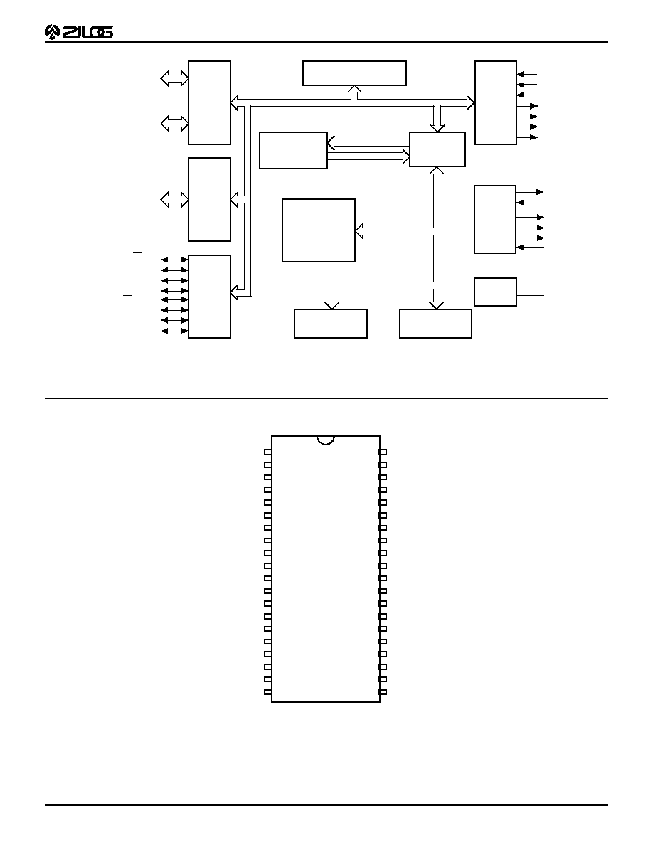
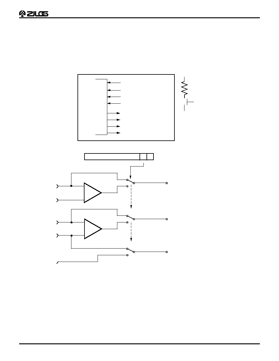
with 8-bit and 16-bit counter/timers (Figure 1). Also includ-
ed are a large number of user-selectable modes, and two
on-board comparators to process analog signals with sep-
arate reference voltages (Figure 2).
Notes:
All Signals with a preceding front slash, "/", are ac-
tive Low, e.g., B//W (WORD is active Low); /B/W (BYTE is
active Low, only).
Power connections follow conventional descriptions be-
low:
Connection
Circuit
Device
Power
V
CC
V
DD
Ground
GND
V
SS
Figure 1. Z86E7X Counter/Timer Block Diagram
HI16
LO16
16-Bit
T16
TC16H
TC16L
HI8
LO8
And/Or
Logic
Clock
Divider
Glitch
Filter
Edge
Detect
Circuit
8-Bit
T8
TC8H
TC8L
8
8
16
8
Input
SCLK
1 2 4
8
Timer 16
Timer 8/16
Timer 8
8
8
8
8
8
Z86E72/E73
OTP IR Microcontrollers
DS96LVO1100
P R E L I M I N A R Y
1-3
1
PIN DESCRIPTION
Figure 2. Z86E7X Functional Block Diagram
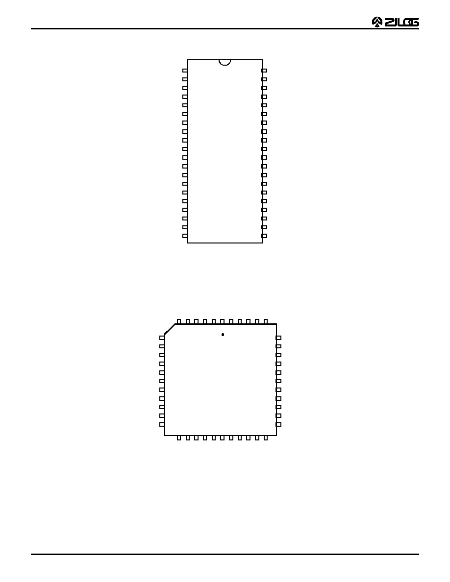
Figure 3. 40-Pin DIP Pin Assignments (Standard Mode)
Port 0
P00
P01
P02
P03
P04
P05
P06
P07
P10
P11
P12
P13
P14
P15
P16
P17
P20
P21
P22
P23
P24
P25
P26
P27
P31
P32
P33
/AS
/DS
R/W
/RESET
Port 3
Port 1
Port 2
Register File
256 or 768 x 8-Bit
ROM
16K/32K x 8
Z8 Core
Register Bus
Internal
Address Bus
Internal Data Bus
Expanded
Register
File
Expanded
Register Bus
Counter/Timer 8
8-Bit
Counter/Timer 16
16-Bit
Machine
Timing
&
Instruction
Control
Power
XTAL
VDD
VSS
P34
P35
P36
P37
4
4
8
I/O Bit
Programmable
R//W
P25
P26
P27
P04
P05
P06
P14
P15
P07
VDD
P16
P17
XTAL2
XTAL1
P31
P32
P33
P34
/AS
/DS
P24
P23
P22
P21
P20
P03
P13
P12
VSS
P02
P11
P10
P01
P00
Pref1
P36
P37
P35
/RESET
40
Z86E72/73
DIP
1
20
21
2
3
4
5
6
7
8
9
10
11
12
13
14
15
16
17
18
19
39
38
37
36
35
34
33
32
31
30
29
28
27
26
25
24
23
22
Z86E72/E73
OTP IR Microcontrollers
1-4
P R E L I M I N A R Y
DS96LVO1100
PIN DESCRIPTION
(Continued)
Figure 4. 40-Pin DIP Pin Assignments (EPROM Mode)
NC
A13
A14
/PGM
A4
A5
A6
D4
D5
A7
VDD
D6
D7
NC
NC
/OE
EPM
VPP
NC
NC
NC
A12
A11
A10
A9
A8
A3
D3
D2
VSS
A2
D1
D0
A1
A0
/CE
NC
NC
NC
NC
40
Z86E72/73
DIP
1
20
21
2
3
4
5
6
7
8
9
10
11
12
13
14
15
16
17
18
19
39
38
37
36
35
34
33
32
31
30
29
28
27
26
25
24
23
22
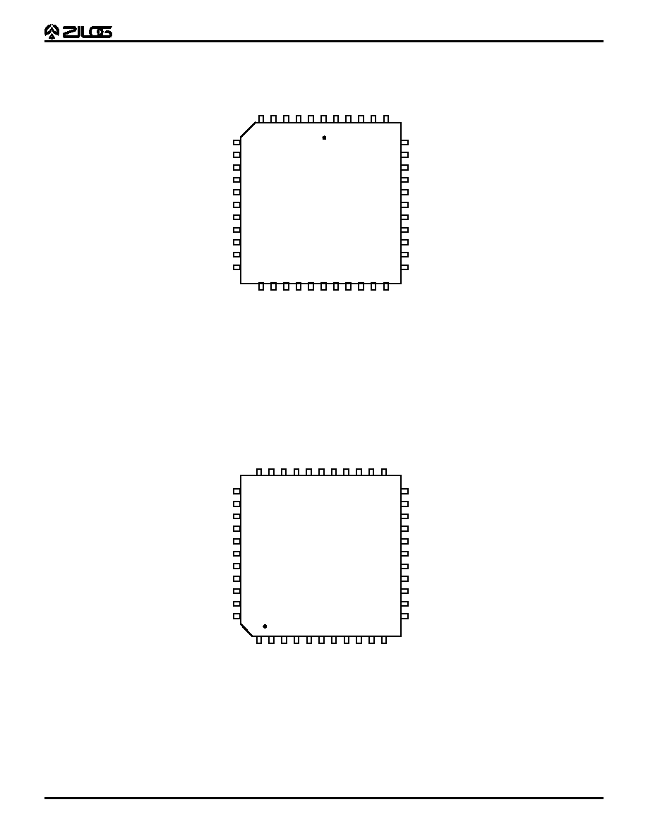
Figure 5. 44-Pin PLCC Pin Assignments (Standard Mode)
Z86E72/73
PLCC
7
8
9
10
11
12
13
14
15
16
17
P21
P22
P23
P24
/DS
R//RL
R//W
P25
P26
P27
P04
Pref1
P36
P37
P35
/RESET
VSS
/AS
P34
P33
P32
P31
P05
P06
P14
P15
P07
VDD
VDD
P16
P17
XT
AL2
XT
AL1
P20
P03
P13
P12
VSS
VSS
P02
P11
P10
P01
P00
1
28
18
40
6
39
38
37
36
35
34
33
32
31
30
29
20
22
24
26
4
42
Z86E72/E73
OTP IR Microcontrollers
DS96LVO1100
P R E L I M I N A R Y
1-5
1
Figure 6. 44-Pin PLCC Pin Assignments (EPROM Mode)
Z86E72/73
PLCC
7
8
9
10
11
12
13
14
15
16
17
A9
A10
A11
A12
NC
NC
NC
A13
A14
/PGM
A4
/CE
NC
NC
NC
NC
SCC
NC
NC
VPP
EPM
/OE
P05
P06
P14
P15
P07
VDD
VDD
P16
P17
XT
AL2
XT
AL1
A8
A3
D3
D2
VSS
VSS
A2
D1
D0
A2
A0
1
28
18
40
6
39
38
37
36
35
34
33
32
31
30
29
20
22
24
26
4
42
Figure 7. 44-Pin QFP Pin Assignments (Standard Mode)
34
35
36
37
38
39
40
41
42
43
44
P21
P22
P23
P24
/DS
R//RL
R//W
P25
P26
P27
P04
Pref1
P36
P37
P35
/RESET
VSS
/AS
P34
P33
P32
P31
P05
P06
P14
P15
P07
VDD
VDD
P16
P17
XT
AL2
XT
AL1
P20
P03
P13
P12
VSS
VSS
P02
P11
P10
P01
P00
1
23
33
Z86E72/73
QFP
11
22
21
20
19
18
17
16
15
14
13
12
25
27
29
31
9
7
5
3
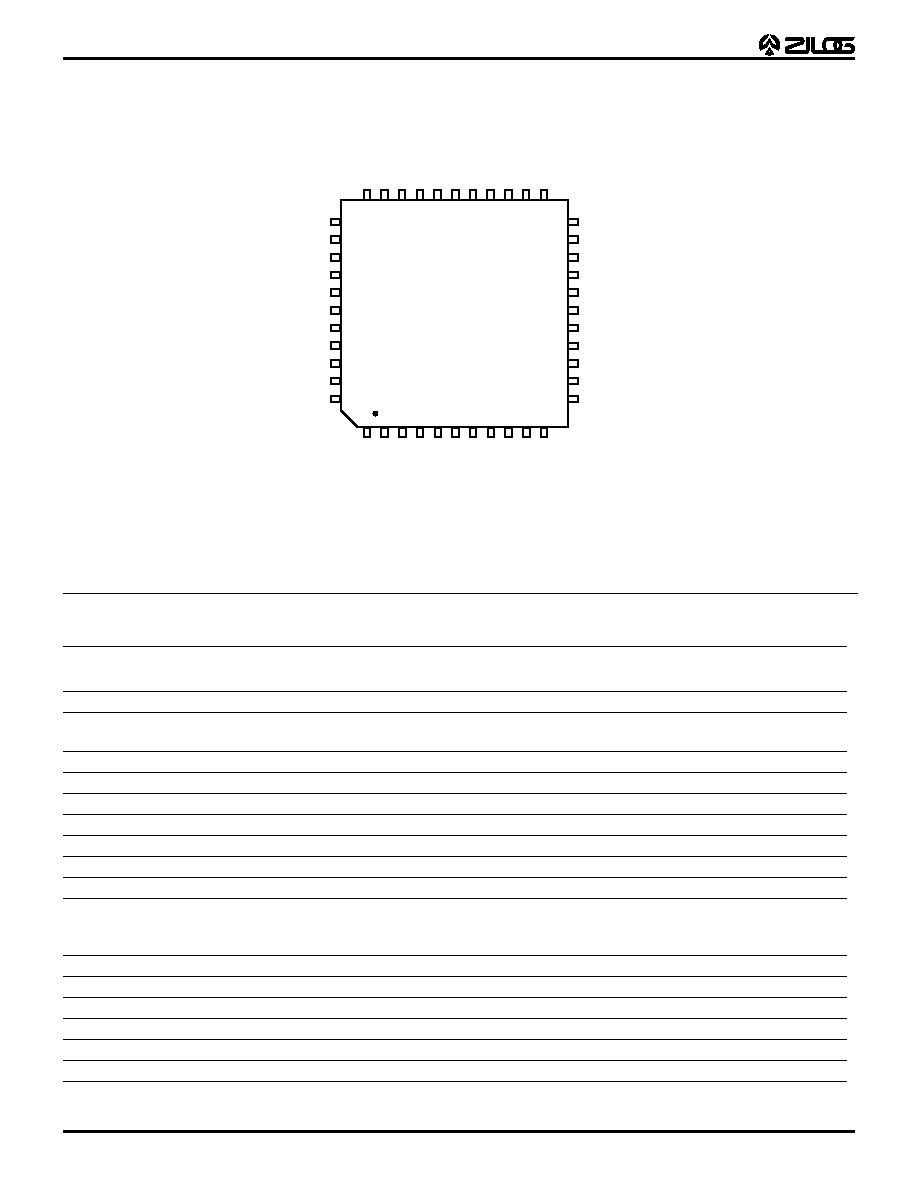
Z86E72/E73
OTP IR Microcontrollers
1-6
P R E L I M I N A R Y
DS96LVO1100
PIN DESCRIPTION
(Continued)
Figure 8. 44-Pin QFP Pin Assignments (EPROM Mode)
34
35
36
37
38
39
40
41
42
43
44
A9
A10
A11
A12
N/C
N/C
N/C
A13
A14
/PGM
A4
/CE
N/C
N/C
N/C
N/C
VSS
N/C
N/C
VPP
EPM
/OE
A5
A6
D4
D5
A7
VDD
VDD
D6
D7
XT
AL2
XT
AL1
A8
A3
D3
D2
VSS
VSS
A2
D1
D0
A1
A0
1
23
33
Z86E72/73
QFP
11
22
21
20
19
18
17
16
15
14
13
12
3
5
7
9
31
29
27
25
Table 1. Pin Identification (Standard Mode)
40-Pin
DIP #
44-Pin
PLCC #
44-Pin
QFP #
Symbol
Direction
Description
26
40
23
P00
Input/Output
Port 0 is Nibble Programmable.
27
41
24
P01
Input/Output
Port 0 can be configured as A15-A8
external program
30
44
27
P02
Input/Output
34
5
32
P03
Input/Output
ROM Address Bus.
5
17
44
P04
Input/Output
Port 0 can be configured as a
6
18
1
P05
Input/Output
mouse/trackball input.
7
19
2
P06
Input/Output
10
22
5
P07
Input/Output
28
42
25
P10
Input/Output
Port 1 is byte programmable.
29
43
26
P11
Input/Output
Port 1 can be configured as multiplexed
A7-A0/D7-D0 external program ROM
Address/Data Bus
32
3
30
P12
Input/Output
33
4
31
P13
Input/Output
8
20
3
P14
Input/Output
.
9
21
4
P15
Input/Output
12
25
8
P16
Input/Output
13
26
9
P17
Input/Output

Z86E72/E73
OTP IR Microcontrollers
1-7
P R E L I M I N A R Y
DS96LVO1100
35
6
33
P20
Input/Output
Port 2 pins are individually configurable
as input or output
36
7
34
P21
Input/Output
37
8
35
P22
Input/Output
38
9
36
P23
Input/Output
39
10
37
P24
Input/Output
2
14
41
P25
Input/Output
3
15
42
P26
Input/Output
4
16
43
P27
Input/Output
16
29
12
P31
Input
IRQ2/Modulator input
17
30
13
P32
Input
IRQ0
18
31
14
P33
Input
IRQ1
19
32
15
P34
Output
T8 output
22
36
19
P35
Output
T16 output
24
38
21
P36
Output
T8/T16 output
23
37
20
P37
Output
20
33
16
/AS
Output
Address Strobe
40
11
38
/DS
Output
Data Strobe
1
13
40
R//W
Output
Read/Write
21
35
18
/RESET
Input
Reset
15
28
11
XTAL1
Input
Crystal, Oscillator Clock
14
27
10
XTAL2
Output
Crystal, Oscillator Clock
11
23, 24
6, 7
V
DD
Power Supply
31
1, 2, 34
17, 28, 29
V
SS
Ground
25
39
22
Pref1
Input
Comparator 1 Reference
NC
12
39
R//RL
Input
ROM//ROMless
Table 1. Pin Identification (Standard Mode)
40-Pin
DIP #
44-Pin
PLCC #
44-Pin
QFP #
Symbol
Direction
Description

Z86E72/E73
OTP IR Microcontrollers
1-8
P R E L I M I N A R Y
DS96LVO1100
PIN DESCRIPTION
(Continued)
Table 2. Z86E72/73 40-Pin DIP Identification (EPROM Mode)
40-Pin #
Symbol
Function
Direction
1
N/C
Not Connected
2-3
A13-14
Address 13,14
Input
4
/PGM
Program Mode
Input
5-7
A4-A6
Address 4,5,6
Input
8-9
D4-D5
Data 4,5
Input/Output
10
A7
Address 7
Input
11
V
DD
Power Supply
12-13
D6-D7
Data 6,7
Input/Output
14-15
N/C
Not Connected
16
/OE
Output Enable
Input
17
EPM
EPROM Prog.Mode
Input
18
V
PP
Prog. Voltage
Input
19-24
N/C
Not Connected
25
/CE
Chip Enable
Input
26-27
A0-A1
Address 0,1
Input
28-29
D0-D1
Data 0, 1
Input/Output
30
A2
Address 2
Input
31
V
SS
Ground
32-33
D2-D3
Data 2,3
Input/Output
34
A3
Address 3
Input
35-39
A8-A12
Address 8,9,10,11,12
Input
40
N/C
Not Connected
Z86E72/E73
OTP IR Microcontrollers
DS96LVO1100
P R E L I M I N A R Y
1-9
1
Table 3. Z86E72/73 44-Pin QFP/PLCC Pin Identification(EPROM Mode)
44-Pin
QFP
44-Pin
PLCC
Symbol
Function
Direction
1-2
18-19
A5-A6
Address 5,6
Input
3-4
20-21
D4-D5
Data 4,5
Input/Output
5
22
A7
Address 7
Input
6-7
23-24
V
DD
Power Supply
8-9
25-26
D6-D7
Data 6,7
Input/Output
10
27
XTAL2
Crystal Oscillator Clock
11
28
XTAL1
Crystal Oscillator Clock
12
29
/OE
Output Enable
Input
13
30
EPM
EPROM Prog. Mode
Input
14
31
V
PP
Prog. Voltage
Input
15-16
32-33
N/C
Not Connected
17
34
V
SS
Ground
18-21
35-38
N/C
Not Connected
22
39
/CE
Chip Select
Input
23-24
40-41
A0-A1
Address 0,1
Input
25-26
42-43
D0-D1
Data 0,1
Input/Output
27
44
A2
Address 2
Input
28-29
1-2
V
SS
Ground
30-31
3-4
D2-D3
Data 2, 3
Input/Output
32
5
A3
Address 3
Input
33-37
6-10
A8-A12
Address 8,9,10,11,12
Input
38-40
11-13
N/C
Not Connected
41-42
14-15
A13-A14
Address 13,14
Input
43
16
/PGM
Prog. Mode
Input
44
17
A4
Address 4
Input

Z86E72/E73
OTP IR Microcontrollers
1-10
P R E L I M I N A R Y
DS96LVO1100
ABSOLUTE MAXIMUM RATINGS
Stresses greater than those listed under Absolute Maxi-
mum Ratings may cause permanent damage to the de-
vice. This is a stress rating only; operation of the device at
any condition above those indicated in the operational sec-
tions of these specifications is not implied. Exposure to ab-
solute maximum rating conditions for an extended period
may affect device reliability.
STANDARD TEST CONDITIONS
The characteristics listed below apply for standard test
conditions as noted. All voltages are referenced to GND.
Positive current flows into the referenced pin (Figure 13).
CAPACITANCE
T
A
= 25
∞
C, V
CC
= GND = 0V, f = 1.0 MHz, unmeasured pins returned to GND.
Symbol
Description
Min
Max
Units
V
CC
Supply Voltage (*)
≠0.3
+7.0
V
T
STG
Storage Temp.
≠65
∞
+150
∞
C
T
A
Oper. Ambient Temp.
C
Notes:
* Voltage on all pins with respect to GND.
See Ordering Information.
Figure 9. Test Load Diagram
From Output
Under Test
150 pF
I
Parameter
Max
Input capacitance
12 pF
Output capacitance
12 pF
I/O capacitance
12 pF

Z86E72/E73
OTP IR Microcontrollers
DS96LVO1100
P R E L I M I N A R Y
1-11
1
DC CHARACTERISTICS
Preliminary
T
A
= 0
∞
C to +70
∞
C
Typical
Sym.
Parameter
V
CC
Min
Max
@ 25
∞
C
Units
Conditions
Max Input Voltage
3.0V
5.5V
7
7
V
V
I
IN
250
µ
A
I
IN
250
µ
A
V
CH
Clock Input
High Voltage
3.0V
5.5V
0.9 V
CC
0.9 V
CC
V
CC
+ 0.3
V
CC
+ 0.3
V
V
Driven by External
Clock Generator
V
CL
Clock Input
Low Voltage
3.0V
5.5V
V
SS
≠0.3
V
SS
≠0.3
0.2 V
CC
0.2 V
CC
V
V
Driven by External
Clock Generator
V
IH
Input High Voltage
3.0V
5.5V
0.7 V
CC
0.7 V
CC
V
CC
+ 0.3
V
CC
+ 0.3
0.5 V
CC
0.5 V
CC
V
V
V
IL
Input Low Voltage
3.0V
5.5V
V
SS
≠0.3
V
SS
≠0.3
0.2 V
CC
0.2 V
CC
0.5 V
CC
0.5 V
CC
V
V
V
OH1
Output High Voltage
3.0V
5.5V
V
CC
≠0.4
V
CC
≠0.4
2.9
5.4
V
V
I
OH
= ≠0.5 mA
I
OH
= ≠0.5 mA
V
OH2
Output High Voltage
(P00,P01,P36, P37)
3.0V
5.5V
V
CC
0.7
V
CC
0.7
V
V
I
OH
= ≠7 mA
I
OH
= ≠7 mA
V
OL1
Output Low Voltage
3.0V
5.5V
0.4
0.4
0.1
0.2
V
V
I
OL
= 1.0 mA
I
OL
= 4.0 mA
V
OL2*
Output Low Voltage
3.0V
5.5V
0.8
0.8
0.5
0.3
V
V
I
OL
= 5.0 mA
I
OL
= 7.0 mA
V
OL2
Output Low Voltage
(P00, P01, P36,P37)
3.0V
5.5V
0.8
0.8
0.3
0.2
V
V
I
OL
= 10 mA
I
OL
= 10 mA
V
RH
Reset Input
High Voltage
3.0V
5.5V
0.8 V
CC
0.8 V
CC
V
CC
V
CC
1.5
2.5
V
V
V
Rl
Reset Input
Low Voltage
3.0V
5.5V
V
SS
≠0.3
V
SS
≠0.3
0.2 V
CC
0.2 V
CC
0.9
1.8
V
OFFSET
Comparator Input
Offset Voltage
3.0V
5.5V
25
25
10
10
mV
mV
I
IL
Input Leakage
3.0V
5.5V
≠1
≠1
1
1
< 1
< 1
µ
A
µ
A
V
IN
= 0V, V
CC
V
IN
= 0V, V
CC
I
OL
Output Leakage
3.0V
5.5V
≠1
≠1
1
1
< 1
< 1
µ
A
µ
A
V
IN
= 0V, V
CC
V
IN
= 0V, V
CC
I
IR
Reset Input Current
3.0V
5.5V
≠230
≠400
≠50
≠80
µ
A
µ
A
I
CC
Supply Current
(WDT off)
3.0V
5.5V
10
15
4
10
mA
mA
@ 8.0 MHz
@ 8.0 MHz

Z86E72/E73
OTP IR Microcontrollers
1-12
P R E L I M I N A R Y
DS96LVO1100
DC CHARACTERISTICS (Continued)
T
A
= 0
∞
C to +70
∞
C
Typical
Sym.
Parameter
V
CC
Min
Max
@ 25
∞
C
Units
Conditions
Notes
I
CC1
Standby Current
(WDT Off)
3.0V
5.5V
3
5
1
4
mA
mA
HALT Mode
V
IN
= 0V, V
CC
@ 8.0
MHz
HALT Mode
V
IN
= 0V, V
CC
@ 8.0 MHz
1,2
1,2
3.0V
5.5V
2
4
0.8
2.5
mA
mA
Clock Divide-by-16 @
8.0 MHz
Clock Divide-by-16 @
8.0 MHz
1,2
1,2
I
CC2
Standby Current
3.0V
5.5V
8
10
2
3
µ
A
µ
A
STOP Mode
V
IN
= O
V
, V
CC
WDT is not Running
STOP Mode
V
IN
= 0V, V
CC
WDT is not Running
3,5
3,5
3.0V
5.5V
500
800
310
600
µ
A
µ
A
STOP Mode
V
IN
= 0V, V
CC
WDT is Running
3,5
T
POR
Power-On Reset
3.0V
5.5V
12
5
75
20
18
7
ms
ms
Vram
Static RAM Data
Retention Voltage
Vram
0.8
0.5
V
6
V
LV
(Vbo)
V
CC
Low Voltage
Protection
2.15
1.7
V
8 MHz max
Ext. CLK Freq.
4
Notes:
I
CC1
Crystal/Resonator
External Clock Drive
Typ
3.0 mA
0.3 mA
Max
5
5
Unit
mA
mA
Frequency
8.0 MHz
8.0 MHz
1. All outputs unloaded, inputs at rail.
2. CL1 = CL2 = 100 pF
3. Same as note [4] except inputs at V
CC
.
4. The V
LV
increases as the temperature decreases.
5. Oscillator stopped.
6. Oscillator stops when VCC falls below Vlv limit
7. 32 kHz clock driver input.
* All Outputs excluding P00, P01, P36, and P37.
Z86E72/E73
OTP IR Microcontrollers
DS96LVO1100
P R E L I M I N A R Y
1-13
1
AC CHARACTERISTICS
External I/O or Memory Read and Write Timing
Figure 10. External I/O or Memory Read/Write Timing
R//W
9
12
18
3
16
13
4
5
8
11
6
17
10
15
7
14
2
1
Port 0, /DM
Port 1
/AS
/DS
(Read)
Port 1
/DS
(Write)
A7 - A0
D7 - D0 IN
D7 - D0 OUT
A7 - A0
19
20

Z86E72/E73
OTP IR Microcontrollers
1-14
P R E L I M I N A R Y
DS96LVO1100
AC CHARACTERISTICS
Preliminary
External I/O or Memory Read and Write Timing Table
T
A
= 0
∞
C to +70
∞
C
16 MHz
No. Symbol
Parameter
V
CC
Min.
Max.
Units
Notes
1
TdA(AS)
Address Valid to
/AS Rising Delay
3.0V
5.5V
55
55
ns
ns
2
2
TdAS(A)
/AS Rising to Address Float Delay
3.0V
5.5V
70
70
ns
ns
2
3
TdAS(DR)
/AS Rising to Read Data Required Valid
3.0V
5.5V
400
400
ns
ns
1,2
1,2
4
TwAS
/AS Low Width
3.0V
5.5V
80
80
ns
ns
2
2
5
Td
Address Float to
/DS Falling
3.0V
5.5V
0
0
ns
ns
6
TwDSR
/DS (Read) Low Width
3.0V
5.5V
300
300
ns
ns
1,2
7
TwDSW
/DS (Write) Low Width
3.0V
5.5V
165
165
ns
ns
1,2
8
TdDSR(DR)
/DS Falling to Read Data Required Valid
3.0V
5.5V
260
260
ns
ns
1,2
9
ThDR(DS)
Read Data to
/DS Rising Hold Time
3.0V
5.5V
0
0
ns
ns
10
TdDS(A)
/DS Rising to Address Active Delay
3.0V
5.5V
85
95
ns
ns
2
11
TdDS(AS)
/DS Rising to /AS
Falling Delay
3.0V
5.5V
60
70
ns
ns
2
12
TdR/W(AS)
R//W Valid to /AS
Rising Delay
3.0V
5.5V
70
70
ns
ns
2
13
TdDS(R/W)
/DS Rising to
R//W Not Valid
3.0V
5.5V
70
70
ns
ns
2
14
TdDW(DSW) Write Data Valid to /DS Falling (Write)
Delay
3.0V
5.5V
80
80
ns
ns
2
15
TdDS(DW)
/DS Rising to Write
Data Not Valid Delay
3.0V
5.5V
70
80
ns
ns
2
16
TdA(DR)
Address Valid to Read Data Required
Valid
3.0V
5.5V
475
475
ns
ns
1,2
17
TdAS(DS)
/AS Rising to
/DS Falling Delay
3.0V
5.5V
100
100
ns
ns
2
2
18
TdDM(AS)
/DM Valid to /AS
Falling Delay
3.0V
5.5V
55
55
ns
ns
2
19
TdDS(DM)
/DS Rise to
/DM Valid Delay
3.0V
5.5V
70
70
ns
ns
20
ThDS(A)
/DS Rise to Address Valid Hold Time
3.0V
5.5V
70
70
ns
ns
Notes:
1. When using extended memory timing add 2 TpC.
2. Timing numbers given are for minimum TpC.
Standard Test Load
All timing references use 0.9 V
CC
for a logic 1 and 0.1 V
CC
for a logic 0.
Z86E72/E73
OTP IR Microcontrollers
DS96LVO1100
P R E L I M I N A R Y
1-15
1
AC CHARACTERISTICS
Additional Timing Diagram
Figure 11. Additional Timing
Clock
1
3
4
8
2
2
3
T
IRQ
IN
N
6
5
7
7
Clock
Setup
10
9
Stop
Mode
Recovery
Source
11

Z86E72/E73
OTP IR Microcontrollers
1-16
P R E L I M I N A R Y
DS96LVO1100
AC CHARACTERISTICS
Preliminary
Additional Timing Table
T
A
= 0
∞
C to +70
∞
C
No
Symbol
Parameter
V
CC
Min
Max
Units
Notes
1
TpC
Input Clock Period
3.0V
5.5V
121
121
DC
DC
ns
ns
1
1
2
TrC,TfC
Clock Input Rise and Fall Times
3.0V
5.5V
25
25
ns
ns
1
1
3
TwC
Input Clock Width
3.0V
5.5V
37
37
ns
ns
1
4
TwTinL
Timer Input Low Width
3.0V
5.5V
100
70
ns
ns
1
5
TwTinH
Timer Input High Width
3.0V
5.5V
3TpC
3TpC
1
6
TpTi
Timer Input Period
3.0V
5.5V
8TpC
8TpC
1
7
TrTin,TfTi Timer Input Rise and Fall Timers
3.0V
5.5V
100
70
ns
ns
1
1
8A
TwIL
Interrupt Request Low Time
3.0V
5.5V
100
70
ns
ns
1,2
1,2
8B
TwIL
Int. Request Low Time
4.5V
5.5V
3TpC
5TpC
1,3
1,3
9
TwIH
Interrupt Request Input High Time
4.5V
5.5V
5TpC
5TpC
1,2
1,2
10
Twsm
Stop-Mode Recovery Width Spec
3.0V
5.5V
3.0V
5.5V
12
12
5TpC
5TpC
ns
ns
7
7
6
6
11
Tost
Oscillator Start-up Time
3.0V
5.5V
5TpC
5TpC
4
12
Twdt
Watch-Dog Timer Delay Time
(5 ms)
3.0V
5.5V
12
5
75
20
ms
ms
(10 ms)
3.0V
5.5V
25
10
150
40
ms
ms
(20 ms)
3.0V
5.5V
50
20
300
80
ms
ms
(80 ms)
3.0V
5.5V
225
80
1200
320
ms
ms
Notes:
1. Timing Reference uses 0.9 V
CC
for a logic 1 and 0.1 V
CC
for a logic 0.
2. Interrupt request through Port 3 (P33-P31).
3. Interrupt request through Port 3 (P30).
4. SMR ≠ D5 = 0
5. Reg. WDTMR
6. Reg. SMR ≠ D5 = 0
7. Reg. SMR ≠ D5 = 1
Z86E72/E73
OTP IR Microcontrollers
DS96LVO1100
P R E L I M I N A R Y
1-17
1
AC CHARACTERISTICS
Handshake Timing Diagrams
Figure 12. Input Handshake Timing
Data In
1
3
4
5
6
/DAV
(Input)
RDY
(Output)
Next Data In Valid
Delayed RDY
Delayed DAV
Data In Valid
2
Figure 13. Output Handshake Timing
Data Out
/DAV
(Output)
RDY
(Input)
Next Data Out Valid
Delayed RDY
Delayed DAV
Data Out Valid
7
8
9
10
11

Z86E72/E73
OTP IR Microcontrollers
1-18
P R E L I M I N A R Y
DS96LVO1100
AC CHARACTERISTICS
Preliminary
Handshake Timing Table
T
A
= 0
∞
C to +70
∞
C
16 MHz
Data
No
Symbol
Parameter
V
CC
Min
Max
Direction
1
TsDI(DAV)
Data In Setup Time
4.0V
5.5V
0
IN
IN
2
ThDI(DAV)
Data In Hold Time
4.0V
5.5V
0
0
IN
IN
3
TwDAV
Data Available Width
4.0V
5.5V
155
110
IN
IN
4
TdDAVI(RDY)
DAV Falling to RDY
Falling Delay
4.0V
5.5V
160
115
IN
IN
5
TdDAVId(RDY)
DAV Rising to RDY
Falling Delay
4.0V
5.5V
120
80
IN
IN
6
TdRDYO(DAV)
RDY Rising to DAV
Falling Delay
4.0V
5.5V
0
0
IN
IN
7
TdDO(DAV)
Data Out to DAV
Falling Delay
4.0V
5.5V
63
63
OUT
OUT
8
TdDAV0(RDY)
DAV Falling to RDY
Falling Delay
4.0V
5.5V
0
0
OUT
OUT
9
TdRDY0(DAV)
RDY Falling to DAV
Rising Delay
4.0V
5.5V
160
115
OUT
OUT
10
TwRDY
RDY Width
4.0V
5.5V
110
80
OUT
OUT
11
TdRDY0d(DAV)
RDY Rising to DAV
Falling Delay
4.0V
5.5V
110
80
OUT

Z86E72/E73
OTP IR Microcontrollers
DS96LVO1100
P R E L I M I N A R Y
1-19
1
PIN FUNCTIONS
/DS (Output, active Low). Data Strobe is activated once for
each external memory transfer. For a READ operation,
data must be available prior to the trailing edge of /DS. For
WRITE operations, the falling edge of /DS indicates that
output data is valid.
/AS (Output, active Low). Address Strobe is pulsed once
at the beginning of each machine cycle. Address output is
through Port 0/Port 1 for all external programs. Memory
address transfers are valid at the trailing edge of /AS. Un-
der program control, /AS is placed in the high-impedance
state along with Ports 0 and 1, Data Strobe, and
Read/Write.
XTAL1 Crystal 1 (time-based input). This pin connects a
parallel-resonant crystal, ceramic resonator, LC, or RC
network or an external single-phase clock to the on-chip
oscillator input.
XTAL2 Crystal 2 (time-based output). This pin connects a
parallel-resonant, crystal, ceramic resonant, LC, or RC
network to the on-chip oscillator output.
R//W Read/Write (output, write Low). The R//W signal is
Low when the CCP is writing to the external program or
data memory.
R//RL (input). This pin, when connected to GND, disables
the internal ROM and forces the device to function as a
ROMless Z8. (Note that, when left unconnected or pulled
high to V
CC
, the part functions normally as a Z8 ROM ver-
sion.)
Port 0 (P07-P00). Port 0 is an 8-bit, bidirectional, CMOS
compatible port. These eight I/O lines are configured un-
der software control as a nibble I/O port, or as an address
port for interfacing external memory. The output drivers
are push-pull. Port 0 is placed under handshake control. In
this configuration, Port 3, lines P32 and P35 are used as
the handshake control /DAV0 and RDY0. Handshake sig-
nal direction is dictated by the I/O direction to Port 0 of the
upper nibble P07-P04. The lower nibble must have the
same direction as the upper nibble.
For external memory references, Port 0 can provide ad-
dress bits A11-A8 (lower nibble) or A15-A8 (lower and up-
per nibble) depending on the required address space. If
the address range requires 12 bits or less, the upper nibble
of Port 0 can be programmed independently as I/O while
the lower nibble is used for addressing. If one or both nib-
bles are needed for I/O operation, they must be configured
by writing to the Port 0 mode register. After a hardware re-
set, Port 0 is configured as an input port.
Port 0 is set in the high-impedance mode if selected as an
address output state along with Port 1 and the control sig-
nals /AS, /DS, and R//W (Figure 8).
A software option is available to program 0.4 V
DD
CMOS
trip inputs on P00-P03. This allows direct interface to
mouse/trackball IR sensors.
An optional 200 kOhm pull-up is available as a software
option of all Port 0 bits with nibble select.
These pull-ups are disabled when configured (bit by bit) as
an output.

Z86E72/E73
OTP IR Microcontrollers
1-20
P R E L I M I N A R Y
DS96LVO1100
PIN FUNCTIONS (Continued)
Figure 14. Port 0 Configuration
Z86LXX
MCU
4
4
Port 0 (I/O or A15 - A8)
Optional
Handshake Controls
/DAV0 and RDY0
(P32 and P35)
OEN
Out
In
PAD
200 k
* Note: On P00 and P07 only.
** POIM, DI, DO Mask Selectable.
*** Refer to the Z86C17 specification for
application information in utilizing these
inputs in a mouse or trackball application.
Mask
Option
In
0.4 VDD
Trip Point Buffer

Z86E72/E73
OTP IR Microcontrollers
DS96LVO1100
P R E L I M I N A R Y
1-21
1
Port 1 (P17-P10). Port 1 is a multiplexed Address (A7-A0)
and Data (D7-D0), CMOS compatible port. Port 1 is dedi-
cated to the Zilog ZBus
Æ
-compatible memory interface.
The operations of Port 1 are supported by the Address
Strobe (/AS) and Data Strobe (/DS) lines, and by the
Read/Write (R//W) and Data Memory (/DM) control lines.
Data memory read/write operations are done through this
port (Figure 20). If more than 256 external locations are re-
quired, Port 0 outputs the additional lines.
Port 1 can be placed in the high-impedance state along
with Port 0, /AS, /DS, and R//W, allowing the Z86L7X to
share common resources in multiprocessor and DMA ap-
plications. Port1 can also be configured for standard port
output mode.
Figure 15. Port 1 Configuration
Port 1
(I/O or AD7 - AD0)
Optional
Handshake Controls
/DAV1 and RDY1
(P33 and P34)
Z86LXX
MCU
8
OEN
Out
In
PAD
Auto Latch
R
500 K

Z86E72/E73
OTP IR Microcontrollers
1-22
P R E L I M I N A R Y
DS96LVO1100
PIN FUNCTIONS (Continued)
Port 2 (P27-P20). Port 2 is an 8-bit, bidirectional, CMOS
compatible I/O port. These eight I/O lines can be indepen-
dently configured under software control as inputs or out-
puts. Port 2 is always available for I/O operation. A soft-
ware option is available to connect eight 200 kOhms
(
±
50%) pull-up resistors on this port. Bits programmed as
outputs are globally programmed as either push-pull or
open-drain. Port 2 may be placed under handshake con-
trol. In this configuration, Port 3 lines, P31 and P36 are
used as the handshake controls lines /DAV2 and RDY2.
The handshake signal assignment for Port 3, lines P31
and P36 is dictated by the direction (input or output) as-
signed to Bit 7, Port 2 (Figure 10).
The CCP wakes up with the eight bits of Port 2 configured
as inputs with open-drain outputs.
Port 2 also has an 8-bit input OR and an AND gate which
can be used to wake up the part. P20 can be programmed
to access the edge selection circuitry (Figure 21).
Figure 16. Port 2 Configuration
Open-Drain
OEN
Out
In
PAD
Port 2 (I/O)
Optional
Handshake Controls
/DAV2 and RDY2
(P31 and P36)
(L72/E72 Only)
Z86LXX
MCU
VCC
200 k
Mask
Option

Z86E72/E73
OTP IR Microcontrollers
DS96LVO1100
P R E L I M I N A R Y
1-23
1
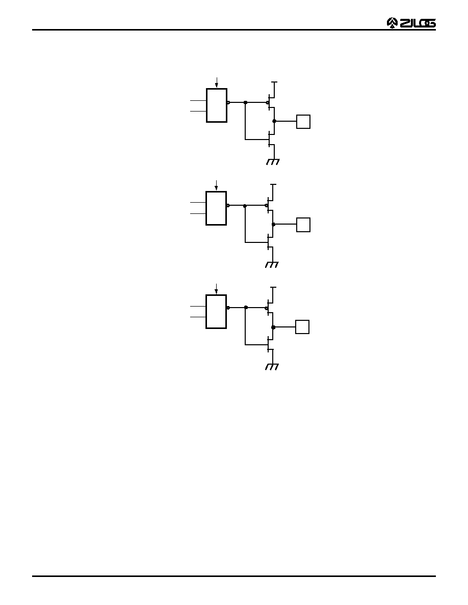
Port 3 (P37-P31). Port 3 is a 7-bit, CMOS compatible three
fixed input and four fixed output port. Port 3 consists of
three fixed input (P33-P31) and four fixed output (P37-
P34), and can be configured under software control for In-
put/Output, Interrupt, Port handshake, Data Memory func-
tions and output from the counter/timers. P31, P32, and
P33 are standard CMOS inputs; outputs are push-pull.
Two on-board comparators process analog signals on P31
and P32 with reference to the voltage on Pref1 and P33.
The analog function is enabled by programming the Port 3
Mode Register (bit 1). P31 and P32 are programmable as
rising, falling, or both edge triggered interrupts (IRQ regis-
ter bits 6 and 7). Pref1 and P33 are the comparator refer-
ence voltage inputs. Access to the Counter Timer edge de-
tection circuit is through P31 or P20 (see CTR1
description).
Port 3 provides the following control functions: handshake
for Ports 0, 1, and 2 (/DAV and RDY); three external inter-
rupt request signals (IRQ2-IRQ0); Data Memory Select
(/DM) (Table 8).
Port 3 also provides output for each of the counter/timers
and the AND/OR Logic. Control is performed by program-
ming bits D5-D4 of CTRI, bit 0 of CTR0 and bit 0 of CTR2.
Figure 17. Port 3 Configuration
P34 OUT
P37 OUT
P32
+
-
P33 (PREF2)
0 = P34, P37 Standard Output
1 = P34, P37 Comparator Output
PCON
D0
P31
+
-
PREF1
P37
PAD
P34
PAD
*
T8
P34 OUT
0 Normal Control
1 8-bit Timer output active
CTR0
D0
Counter/Timer
Reset condition.
*
COMP2
COMP1

Z86E72/E73
OTP IR Microcontrollers
1-24
P R E L I M I N A R Y
DS96LVO1100
PIN FUNCTIONS (Continued)
Comparator Inputs. In Analog Mode, Port 3 (P31 and
P32) have a comparator front end. The comparator refer-
ence is supplied to P33 and Pref1. In this mode, the P33
internal data latch and its corresponding IRQ1 is diverted
to the SMR sources (excluding P31, P32, and P33) as
shown in Figure 37. In digital mode, P33 is used as D3 of
the Port 3 input register which then generates IRQ1 as
shown in Figure 23.
Notes: Comparators are disabled/powered down by enter-
ing STOP mode. For P31-P33 to be used as a Stop-Mode
recovery source, these inputs must be placed into digital
mode.
Comparator Outputs. These may be programmed to be
outputted on P34 and P37 through the PCON register (Fig-
ure 22).
/RESET (Input, active Low). Initializes the MCU. Reset is
accomplished either through Power-On, Watch-Dog Tim-
er, Stop-Mode Recovery, Low Voltage detection, or exter-
nal reset. During Power-On Reset and Watch-Dog Timer
Reset, the internally generated reset drives the reset pin
Low for the POR time. Any devices driving the reset line
should be open-drain in order to avoid damage from a pos-
sible conflict during reset conditions. Pull-up is provided in-
ternally. There is no condition internal to the L7X that will
not allow an external reset to occur.
Table 4. Pin Assignments
Pin
I/O
C/T
Comp.
Int.
P0 HS
P1 HS
P2 HS
Ext
Pref1
IN
RF1
P31
IN
IN
AN1
IRQ2
D/R
P32
IN
AN2
IRQ0
D/R
P33
IN
RF2
IRQ1
D/R
P34
OUT
T8
A01
R/D
D/M
P35
OUT
T16
R/D
P36
OUT
T8/16
R/D
P37
OUT
A02
P20
I/O
IN
Notes:
HS = Handshake Signals
D = /DAV
R = RDY
Z86E72/E73
OTP IR Microcontrollers
DS96LVO1100
P R E L I M I N A R Y
1-25
1
After the POR time, /RESET is a Schmitt-triggered input.
To avoid asynchronous and noisy reset problems, the
Z86L7X is equipped with a reset filter of four external
clocks (4TpC). If the external reset signal is less than 4TpC
in duration, no reset occurs. On the fifth clock after the re-
set is detected, an internal RST signal is latched and held
for an internal register count of 18 external clocks, or for
the duration of the external reset, whichever is longer.
During the reset cycle, /DS is held active Low while /AS cy-
cles at a rate of TpC/2. Program execution begins at loca-
tion 000CH, 5-10 TpC cycles after the RST is released. For
Power-On Reset, the typical reset output time is 5 ms. The
Z86E7X devices do not have internal pull resistors on
Port 3 inputs.
Figure 18. Port 3 Configuration
Port 3
(I/O or Handshake)
Z86LXX
MCU
Pref1
P31
P32
P33
P34
P35
P36
P37
Note:
P31, 32, 33 have a 200 K
mask option called Mask
option 3 similar to Mask
options 1 and 2.
200 K
Mask
Option
D1
R247 = P3M
P31 (AN1)
P32 (AN2)
P33 (REF2)
From Stop-Mode
Recovery Source
1 = Analog
0 = Digital
IRQ2, P31 Data Latch
IRQ0, P32 Data Latch
IRQ1, P33 Data Latch
DIG.
AN.
-
+
-
+
PREF1
COMP1
COMP2
Z86E72/E73
OTP IR Microcontrollers
1-26
P R E L I M I N A R Y
DS96LVO1100
PIN FUNCTIONS (Continued)
Figure 19. Port 3 Configuration
VDD
Out 34
T8_Out
CTR0, D0
Pad
Out 35
T16_Out
CTR2, D0
Out 36
T8/16_Out
CTR1, D6
MUX
MUX
MUX
P34
VDD
Pad
P35
VDD
Pad
P36

Z86E72/E73
OTP IR Microcontrollers
DS96LVO1100
P R E L I M I N A R Y
1-27
1
FUNCTIONAL DESCRIPTION
The Z8
Æ
CCP incorporates special functions to enhance
the Z8's functionality in consumer and battery operated ap-
plications.
Reset. The device is reset in one of the following condi-
tions:
1.
Power-On Reset
2.
Watch-Dog Timer
3.
Stop-Mode Recovery Source
4.
Low Voltage Detection
5.
External Reset
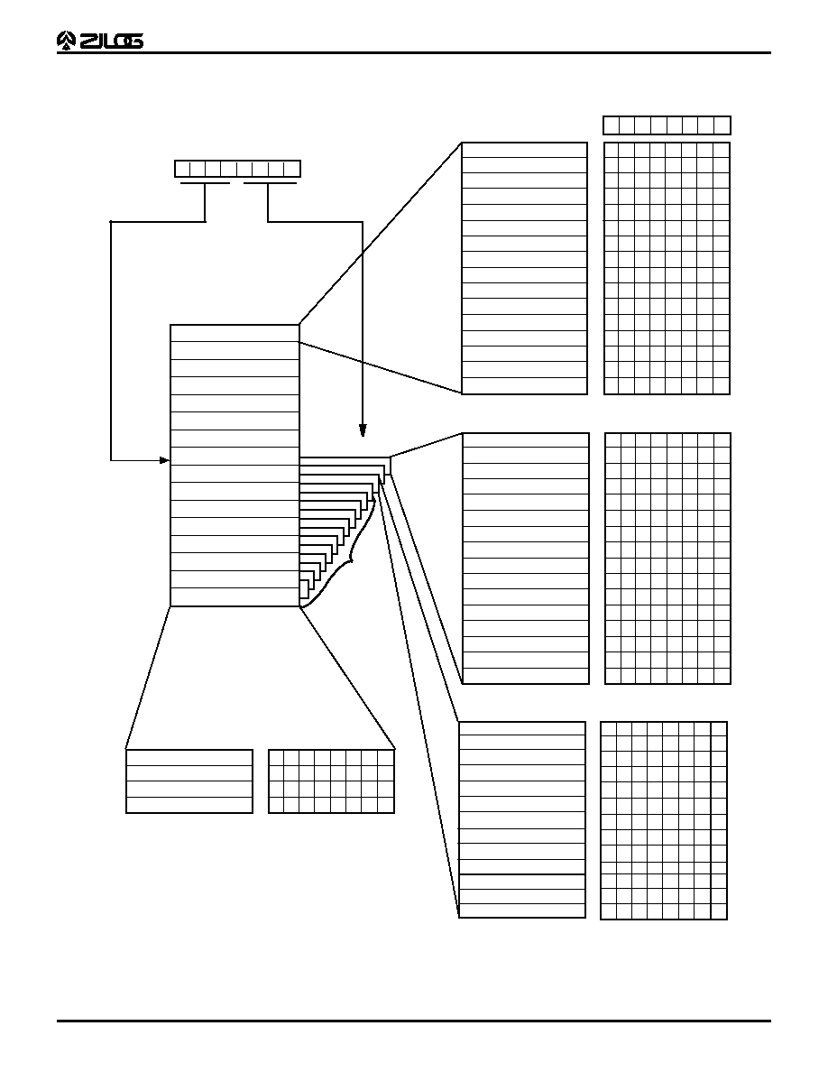
Program Memory. The Z86E72/73 addresses up to
16K/32 Kbytes of internal program memory, with the re-
mainder being external memory (Figure 26). The first 12
bytes of program memory are reserved for the interrupt
vectors. These locations contain five 16-bit vectors that
correspond to the five available interrupts. Addresses of
16K/32K consist of on-chip OTP. At addresses 16K or 32K
and greater, the E72/73 executes external program mem-
ory fetches (refer to external memory timing specifica-
tions).
RAM. The Z86E72 has a 768-byte RAM, 256 bytes make
up the Register file. The remaining 512 bytes make up the
Extended Data RAM. The Z86E73 has just the 256 bytes
of the Register file.
Extended Data RAM. The Extended Data RAM of the
Z86E72 occupies the address range FE00H-FFFFH (512
bytes). This range of addresses FD00H-FFFFH cannot be
used to directly read from or write to external memory. Ac-
cessing the Extended Data RAM is accomplished by using
LDE, LDEI, LDC, or LDCI instructions. Port 1 and Port 0
are free to be set as I/O or ADDR/DATA modes; except
high-impedance when accessing Extended Data RAM. In
addition, if the External Memory uses the same address
range of the Extended Data RAM it can be used as the Ex-
ternal Stack only.
Note: The Extended Data RAM cannot be used as
STACK or instruction/code memory. Accessing the
Extended Data RAM has the following condition: P01M
register bits D4-D3 cannot be set to 11.
Figure 20. Program Memory Map
11
10
9
8
7
6
5
4
3
2
1
0
External ROM
Location of
First Byte of
Instruction
Executed
After RESET
Interrupt
Vector
(Lower Byte)
Interrupt
Vector
(Upper Byte)
Reserved
IRQ4
IRQ4
IRQ3
IRQ3
IRQ2
IRQ2
IRQ1
IRQ1
IRQ0
IRQ0
Reserved
65535
On-Chip
ROM
16384
Reset Start Address
12

Z86E72/E73
OTP IR Microcontrollers
1-28
P R E L I M I N A R Y
DS96LVO1100
FUNCTIONAL DESCRIPTION (Continued)
External Memory. The Z86E72/73 addresses up to 32
Kbytes (minus FD00H-FFFFH) of External Memory begin-
ning at address 8000H (32K+1), (Figure 27). External data
memory is included with, or separated from, the external
program memory space. /DM, an optional I/O function that
is programmed to appear on P34, is used to distinguish be-
tween data and program memory space. The state of the
/DM signal is controlled by the type of instruction being ex-
ecuted. An LDC opcode references PROGRAM (/DM inac-
tive) memory, and an LDE instruction references data
(/DM active Low) memory.
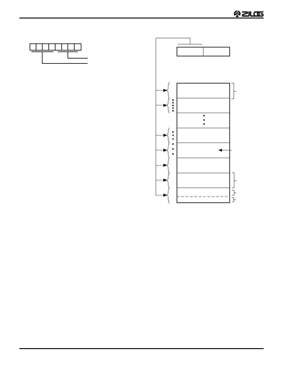
Expanded Register File. The register file has been ex-
panded to allow for additional system control registers,
and for mapping of additional peripheral devices into the
register address area. The Z8 register address space R0
through R15 has been implemented as 16 banks of 16 reg-
isters per bank. These register groups are known as the
ERF (Expanded Register File).
Bits 7-4 of register RP select the working register group.
Bits 3-0 of register RP select the expanded register file
bank. Note that expanded register bank is also referred
to as expanded register group (Figure 24).
The upper nibble of the register pointer (Figure 24) selects
which working register group of 16 bytes in the register file,
out of the possible 256, will be accessed. The lower nibble
selects the expanded register file bank and, in the case of
the Z86LXX family, banks 0, F, and D are implemented. A
0h in the lower nibble will allow the normal register file
(bank 0) to be addressed, but any other value from 1h to
Fh will exchange the lower 16 registers to an expanded
register bank.
For example:
Z86E73: (See Figure 23)
But if:
The counter/timers are mapped into ERF group D. Access
is easily done using the following example:
Figure 21. External Memory Map
65535
0
External
Data
Memory
Not Addressable
32,768
R253 RP = 00H
R0 = Port0
R1 = Port1
R2 = Port2
R3 = Port3
R253 RP = 0DH
R0 = CTRL0
R1 = CTRL1
R2 = CTRL2
R3 = Reserved
LD
RP,#0DH
Select ERF D for access and
register Bank 0 as the working
register group.
LD
R0,#xx
access CTRL0
LD
1,#xx
access CTRL1
LD
RP,#7DH
Select expanded register group
(ERF) group D for access and
register Bank 7 as the working
register bank.
LD
R1,2
CTRL2
register 71H
Z86E72/E73
OTP IR Microcontrollers
DS96LVO1100
P R E L I M I N A R Y
1-29
1
Figure 22. Expanded Register File Architecture
7
6
5
4
3
2
1
0
Working Register
Group Pointer
Expanded Register
Bank/Group Pointer
FF
FO
7F
0F
00
Z8 Register File**
REGISTER POINTER
FF
FE
FD
FC
FB
FA
F9
F8
F7
F6
F5
F4
F3
F2
F1
F0
SPL
SPH
RP
FLAGS
IMR
IRQ
IPR
P01M
P3M
P2M
U
U
0
U
0
0
U
0
0
1
(F) 0F
(F) 0E
(F) 0D
(F) 0C
(F) 0B
(F) 09
(F) 08
(F) 07
(F) 06
(F) 05
(F) 04
(F) 03
(F) 02
(F) 01
(F) 00
WDTMR
SMR
U
U
0
U
U
0
U
1
0
1
U
U
0
U
U
0
U
0
0
1
U
U
0
U
U
0
U
0
0
1
U
U
0
U
U
0
U
1
0
1
U
U
0
U
U
0
U
1
0
1
U
U
0
U
U
0
U
0
0
1
U
U
0
U
U
0
U
1
0
1
U
U
U
0
1
1
0
1
0
0
1
0
0
0
U
0
REGISTER**
EXPANDED REG. BANK/GROUP (F)
RESET CONDITION
REGISTER**
Z8
Æ
STANDARD CONTROL REGISTERS
RESET CONDITION
D7 D6 D5 D4 D3 D2 D1 D0
Reserved
*
*
*
OPT
SMR2
Reserved
Reserved
U
U
U
U
U
U
U
U
U
U
U
U
U
U
U
U
U
U
U
U
U
U
U
U
U
U
U
U
U
U
U
U
0
0
0
0
0
0
0
0
0
U
U
0
0
0
0
0
Reserved
PCON
U
0
*
0
0
0
0
U
U
U
U
U
U
U
U
U
U
U
U
U
U
U
U
U
U
U
U
U
U
U
U
U
U
U
U
REGISTER**
EXPANDED REG. GROUP (0)
RESET CONDITION
(0) 03
P3
(0) 02
P2
(0) 01
P1
(0) 00
P0
U = Unknown
* Will not be reset with a Stop-Mode Recovery
** All addresses are in Hexadecimal
*
*
Will not be reset with a Stop-Mode Recovery, except Bit 0.
Reserved
Reserved
Reserved
Reserved
Reserved
U
0
U
0
0
0
U
U
EXPANDED REG. BANK/GROUP (D)
REGISTER**
(D) 0C
(D) 0B
(D) 0A
(D) 09
(D) 08
(D) 07
(D) 06
(D) 05
(D) 04
(D) 03
(D) 02
Reserved
HI8
L08
HI16
L016
TC16H
TC16L
TC8H
TC8L
Reserved
CTR2
RESET CONDITION
U
U
U
U
U
U
U
U
U
U
U
U
U
U
U
U
U
U
0
U
U
U
U
U
U
U
U
U
U
U
U
U
U
U
U
U
U
U
U
U
U
U
U
U
U
U
U
U
U
U
U
U
U
U
U
U
U
U
U
U
U
U
U
U
U
U
U
U
U
U
U
(D) 01 CTR1
(D) 00 CTR0
0
0
U
U
U
U
U
U
0
U
U
U
U
U
U
Reserved
U
U
U
U
U
U
0
(F) 0A
Reserved
Reserved
Reserved
Reserved
Reserved
Reserved
Reserved
Reserved
Reserved
0
0
0
0
0
0
0
0
Z86E72/E73
OTP IR Microcontrollers
1-30
P R E L I M I N A R Y
DS96LVO1100
FUNCTIONAL DESCRIPTION (Continued)
Register File. The register file (bank 0) consists of four I/O
port registers, 236 general-purpose registers, and 16 con-
trol and status registers (R0-R3, R4-R239, and R240-
R255, respectively), Plus two expanded registers groups
(Banks D and F). Instructions can access registers directly
or indirectly through an 8-bit address field. This allows a
short, 4-bit register address using the Register Pointer
(Figure 23). In the 4-bit mode, the register file is divided
into 16 working register groups, each occupying 16 contin-
uous locations. The Register Pointer addresses the start-
ing location of the active working register group.
Note: Working register group E0-EF of Bank 0 are only
accessed through working registers and indirect address-
ing modes.
Stack. The Z86E7X external data memory or the internal
register file is used for the stack. An 8-bit Stack Pointer
(R255) is used for the internal stack that resides in the gen-
eral-purpose registers (R4-R239). SPH is used as a gen-
eral-purpose register only when using internal stacks.
Note: When SPH is used as a general-purpose register
and Port 0 is in address mode, the contents of SPH will be
loaded into Port 0 whenever the internal stack is accessed.
Figure 23. Register Pointer
D7
D6
D5
D4
D3
D2
D1
D0
Expanded Register File Pointer
Working Register Pointer
R253 RP
Default Setting After Reset = 0000 0000
Figure 24. Register Pointer
The upper nibble of the register file address
provided by the register pointer specifies
the active working-register group
r
7
r
6
r
5
r
4
R253
I/O Ports
Specified Working
Register Group
The lower nibble
of the register
file address
provided by the
instruction points
to the specified
register
r
3
r
2
r
1
r
0
Register Group 0
FF
Register Group 1
2F
1F
0F
00
10
20
F0
R15 to R4
R3 to R0
R15 to R0
R15 to R0
Z86E72/E73
OTP IR Microcontrollers
DS96LVO1100
P R E L I M I N A R Y
1-31
1
COUNTER/TIMER REGISTER DESCRIPTION
Register Description
HI8(D)%0B: Holds the captured data from the output of the
8-bit Counter/Timer0. This register is typically used to hold
the number of counts when the input signal is 1.
L08(D)%0A: Holds the captured data from the output of
the 8-bit Counter/Timer0. This register is typically used to
hold the number of counts when the input signal is 0.
HI16(D)%09: Holds the captured data from the output of
the 16-bit Counter/Timer16. This register holds the MS-
Byte of the data.
L016(D)%08: Holds the captured data from the output of
the 16-bit Counter/Timer16. This register holds the LS-
Byte of the data.
TC16H(D)%07: Counter/Timer2 MS-Byte Hold Register.
TC16L(D)%06: Counter/Timer2 LS-Byte Hold Register.
TC8H(D)%05: Counter/Timer8 High Hold Register.
TC8L(D)%04: Counter/Timer8 Low Hold Register.
Table 5. Expanded Register Group D
(D) %0C
Reserved
(D) % 0B
HI8
(D) % 0A
LO8
(D) %09
HI16
(D) %08
LO16
(D) %07
TC16H
(D) %06
TC16L
(D) %05
TC8H
(D) %04
TC8L
(D) %03
Reserved
(D) %02
CTR2
(D) %01
CTR1
(D) %00
CTR0
Field
Bit Position
Value
Description
T8_Capture_HI
76543210
R/W
Captured Data
No Effect
Field
Bit Position
Value
Description
T8_Capture_L0
76543210
R/W
Captured Data
No Effect
Field
Bit Position
Value
Description
T16_Capture_HI
76543210
R/W
Captured
Data
No Effect
Field
Bit Position
Value
Description
T16_Capture_LO 76543210
R/W
Captured Data
No Effect
Field
Bit Position
Value
Description
T16_Data_HI
76543210
R/W
Data
Field
Bit Position
Value
Description
T16_Data_LO
76543210
R/W
Data
Field
Bit Position
Value
Description
T8_Level_HI
76543210
R/W
Data
Field
Bit Position
Value
Description
T8_Level_LO
76543210
R/W
Data

Z86E72/E73
OTP IR Microcontrollers
1-32
P R E L I M I N A R Y
DS96LVO1100
COUNTER/TIMER REGISTER DESCRIPTION (Continued)
CTR0 (D)00: Counter/Timer8 Control Register.
CTR0: Counter/Timer8 Control Register Description
T8 Enable. This field enables T8 when set (written) to 1.
Single/Modulo-N. When set to 0 (modulo-n), the counter
reloads the initial value when the terminal count is
reached. When set to 1 (single pass), the counter stops
when the terminal count is reached.
Time-Out. This bit is set when T8 times out (terminal count
reached). To reset this bit, a 1 should be written to this lo-
cation.
This is the only way to reset this status condi-
tion, therefore, care should be taken to reset this bit
prior to using/enabling the counter/timers.
Note: Care must be taken when utilizing the OR or AND
commands to manipulate CTR0, bit 5 and CTR1, bits 0
and 1 (Demodulation Mode). These instructions use a
Read-Modify-Write sequence in which the current status
from the CTR0 and CTR1 registers will be ORed or ANDed
with the designated value and then written back into the
registers. Example: When the status of bit 5 is 1, a reset
condition will occur.
T8 Clock. Defines the frequency of the input signal to T8.
Capture_INT_Mask. Set this bit to allow interrupt when
data is captured into either LO8 or HI8 upon a positive or
negative edge detection in demodulation mode.
Counter_INT_Mask. Set this bit to allow interrupt when T8
has a time out.
P34_Out. This bit defines whether P34 is used as a normal
output pin or the T8 output
Field
Bit Position
Value
Description
T8_Enable
7-------
R
W
0*
1
0
1
Counter Disabled
Counter Enabled
Stop Counter
Enable Counter
Single/Modulo
-6------
R/W
0
1
Modulo-N
Single Pass
Time_Out
--5------
R
W
0
1
0
1
No Counter Time-Out
Counter Time-Out Occurred
No Effect
Reset Flag to 0
T8 _Clock
---43---
R/W 0
0
0 1
1 0
1 1
SCLK
SCLK/2
SCLK/4
SCLK/8
Capture_INT_MASK
-----2--
R/W
0
1
Disable Data Capture Int.
Enable Data Capture Int.
Counter_INT_Mask
------1-
R/W
0
1
Disable Time-Out Int.
Enable Time-Out Int.
P34_Out
-------0
R/W
0*
1
P34 as Port Output
T8 Output on P34
Note: *Indicates the value upon Power-On Reset

Z86E72/E73
OTP IR Microcontrollers
DS96LVO1100
P R E L I M I N A R Y
1-33
1
CTR1(D)%01: Controls the functions in common with the T8 and T16.
Field
Bit Position
Value
Description
Mode
7-------
R/W
0*
1
Transmit Mode
Demodulation Mode
P36_Out/
Demodulator_Input
-6------
R/W
0*
1
0
1
Transmit Mode
Port Output
T8/16 Output
Demodulation Mode
P31
P20
T8/T16_Logic/
Edge _Detect
--54----
R/W
0 0
0 1
1 0
1 1
0 0
0 1
1 0
1 1
Transmit Mode
AND
OR
NOR
NAND
Demodulation Mode
Falling Edge
Rising Edge
Both Edges
Reserved
Transmit_Submode/
Glitch_Filter
----32--
R/W
0 0
0 1
1 0
1 1
0 0
0 1
1 0
1 1
Transmit Mode
Normal Operation
Ping-Pong Mode
T16_OUT = 0
T16_OUT = 1
Demodulation Mode
No Filter
4 SCLK Cycle
8 SCLK Cycle
16 SCLK Cycle
Initial_T8_Out/
Rising_Edge
------1-
R/W
R
W
0
1
0
1
0
1
Transmit Mode
T8_OUT is 0 Initially
T8_OUT is 1 Initially
Demodulation Mode
No Rising Edge
Rising Edge Detected
No Effect
Reset Flag to 0
Initial_T16_Out/
Falling _Edge
-------0
R/W
R
W
0
1
0
1
0
1
Transmit Mode
T16_OUT is 0 Initially
T16_OUT is 1 Initially
Demodulation Mode
No Falling Edge
Falling Edge Detected
No Effect
Reset Flag to 0
Note: * Indicates the value upon Power-On Reset.

Z86E72/E73
OTP IR Microcontrollers
1-34
P R E L I M I N A R Y
DS96LVO1100
COUNTER/TIMER REGISTER DESCRIPTION (Continued)
CTR1 Register Description
Mode. If it is 0, the Counter/Timers are in the transmit
mode, otherwise they are in the demodulation mode.
P36_Out/Demodulator_Input. In Transmit Mode, this bit
defines whether P36 is used as a normal output pin or the
combined output of T8 and T16.
In Demodulation Mode, this bit defines whether the input
signal to the Counter/Timers is from P20 or P31.
T8/T16_Logic/Edge _Detect. In Transmit Mode, this field
defines how the outputs of T8 and T16 are combined
(AND, OR, NOR, NAND).
In Demodulation Mode, this field defines which edge
should be detected by the edge detector.
Transmit_Submode/Glitch Filter. In Transmit Mode, this
field defines whether T8 and T16 are in the "Ping-Pong"
mode or in independent normal operation mode. Setting
this field to "Normal Operation Mode" terminates the "Ping-
Pong Mode" operation. When set to 10, T16 is immediately
forced to a 0. When set to 11, T16 is immediately forced
to a 1.
In Demodulation Mode, this field defines the width of the
glitch that should be filtered out.
Initial_T8_Out/Rising_Edge. In Transmit Mode, if 0, the
output of T8 is set to 0 when it starts to count. If 1, the out-
put of T8 is set to 1 when it starts to count. When this bit is
set to 1 or 0, T8_OUT will be set to the opposite state of
this bit. This insures that when the clock is enabled a tran-
sition occurs to the initial state set by CTR1, D1.
In Demodulation Mode, this bit is set to 1 when a rising
edge is detected in the input signal. In order to reset it, a 1
should be written to this location.
Initial_T16 Out/Falling _Edge. In Transmit Mode, if it is 0,
the output of T16 is set to 0 when it starts to count. If it is
1, the output of T16 is set to 1 when it starts to count. This
bit is effective only in Normal or Ping-Pong Mode (CTR1,
D3, D2). When this bit is set, T16_OUT will be set to the
opposite state of this bit. This insures that when the clock
is enabled a transition occurs to the initial state set by
CTR1, D0.
In Demodulation Mode, this bit is set to 1 when a falling
edge is detected in the input signal. In order to reset it, a 1
should be written to this location.
Note: Modifying CTR1, (D1 or D0) while the counters are
enabled will cause un-predictable output from T8/T16 out.

Z86E72/E73
OTP IR Microcontrollers
DS96LVO1100
P R E L I M I N A R Y
1-35
1
CTR2 (D)%02: Counter/Timer16 Control Register.
CTR2 Description
T16_Enable. This field enables T16 when set to 1.
Single/Modulo-N. In Transmit Mode, when set to 0, the
counter reloads the initial value when terminal count is
reached. When set to 1, the counter stops when the termi-
nal count is reached.
In Demodulation Mode, when set to 0 , T16 captures and
reloads on detection of all the edges; when set to 1, T16
captures and detects on the first edge, but ignores the sub-
sequent edges. For details, see the description of T16 De-
modulation Mode.
Time_Out. This bit is set when T16 times out (terminal
count reached). In order to reset it, a 1 should be written to
this location.
T16_Clock. Defines the frequency of the input signal to
Counter/Timer16.
Capture_INT_Mask. Set this bit to allow interrupt when
data is captured into LO16 and HI16.
Counter_INT_Mask. Set this bit to allow interrupt when
T16 times out.
P35_Out. This bit defines whether P35 is used as a normal
output pin or T16 output.
Field
Bit Position
Value
Description
T16_Enable
7-------
R
W
0*
1
0
1
Counter Disabled
Counter Enabled
Stop Counter
Enable Counter
Submode/Modulo-N
-6------
R/W
0
1
0
1
Transmit Mode
Modulo-N
Single Pass
Demodulation Mode
T16 Recognizes Edge
T16 Does Not Recognize Edge
Time_Out
--5-----
R
W
0
1
0
1
No Counter Time-Out
Counter Time-Out Occurred
No Effect
Reset Flag to 0
T16 _Clock
---43---
R/W
00
01
10
11
SCLK
SCLK/2
SCLK/4
SCLK/8
Capture_INT_Mask
-----2--
R/W
0
1
Disable Data Capture Int.
Enable Data Capture Int.
Counter_INT_Mask
------1-
R/W
0
1
Disable Time-Out Int.
Enable Time-Out Int.
P35_Out
-------0
R/W
0*
1
P35 as Port Output
T16 Output on P35
Note: * Indicates the value upon Power-On Reset.
Z86E72/E73
OTP IR Microcontrollers
1-36
P R E L I M I N A R Y
DS96LVO1100
COUNTER/TIMER REGISTER DESCRIPTION (Continued)
SMR2(F) %0D: Stop-Mode Recovery Register 2.
Counter/Timer Functional Blocks
Field
Bit Position
Value
Description
Reserved
7-------
0
Reserved (Must be 0)
Recovery Level
-6------
W
0*
1
Low
High
Reserved
--5-----
0
Reserved (Must be 0)
Source
---432--
W
000*
001
010
011
100
101
110
111
A. POR Only
B. NAND of P23-P20
C. NAND or P27-P20
D. NOR of P33-P31
E. NAND of P33-P31
F. NOR of P33-P31, P00,P07
G. NAND of P33-P31,P00,P07
H. NAND of P33-P31,P22-P20
Reserved
------10
00
Reserved (Must be 0)
Note: * Indicates the value upon Power-On Reset.
Figure 25. Glitch Filter Circuitry
Glitch
Filter
Edge
Detector
CTR1 D5,D4
CTR1 D3,D2
Pos Edge
Neg Edge
MUX
CTR1 D6
P31
P20
Z86E72/E73
OTP IR Microcontrollers
DS96LVO1100
P R E L I M I N A R Y
1-37
1
Input Circuit
The edge detector monitors the input signal on P31 or P20.
Based on CTR1 D5-D4, a pulse is generated at the Pos
Edge or Neg Edge line when an edge is detected. Glitches
in the input signal which have a width less than specified
(CTR1 D3, D2) are filtered out.
T8 Transmit Mode
When T8 is enabled, the output of T8 depends on CTR1,
D1. If it is 0, T8_OUT is 1. If it is 1, T8_OUT is 0.
When T8 is enabled, the output T8_OUT switches to the
initial value (CTR1 D1). If the initial value (CTR1 D1) is 0,
TC8L is loaded, otherwise TC8H is loaded into the
counter. In Single-Pass Mode (CTR0 D6), T8 counts down
to 0 and stops, T8_OUT toggles, the time-out status bit
(CTR0 D5) is set, and a time-out interrupt can be generat-
ed if it is enabled (CTR0 D1) (Figure 33). In Modulo-N
Mode, upon reaching terminal count, T8_OUT is toggled,
but no interrupt is generated. Then T8 loads a new count
(if the T8_OUT level now is 0), TC8L is loaded; if it is 1,
TC8H is loaded. T8 counts down to 0, toggles T8_OUT,
sets the time-out status bit (CTR0 D5) and generates an
interrupt if enabled (CTR0 D1) (Figure 34). This completes
one cycle. T8 then loads from TC8H or TC8L according to
the T8_OUT level, and repeats the cycle.
The user can modify the values in TC8H or TC8L at any
time. The new values take effect when they are loaded.
Care must be taken not to write these registers at the time
the values are to be loaded into the counter/timer, to en-
sure known operation. An initial count of 1 is not allowed (a
non-function will occur). An initial count of 0 will cause TC8
to count from 0 to %FF to %FE (Note, % is used for hexa-
decimal values). Transition from 0 to %FF is not a time-out
condition.
Note: Using the same instructions for stopping the
counter/timers and setting the status bits is not rec-
ommended. Two successive commands, first stopping
the counter/timers, then resetting the status bits is neces-
sary. This is required because it takes one counter/timer
clock interval for the initiated event to actually occur.
Figure 26. 8-Bit Counter/Timer Circuits
Z8 Data Bus
Pos Edge
Neg Edge
CTR0 D2
IRQ4
CTR0 D1
T8_OUT
TC8L
TC8H
Clock
Select
SCLK
CTR0 D4, D3
Clock
8-Bit
Counter T8
HI8
LO8
Z8 Data Bus

Z86E72/E73
OTP IR Microcontrollers
1-38
P R E L I M I N A R Y
DS96LVO1100
COUNTER/TIMER REGISTER DESCRIPTION (Continued)
Figure 27. T8_OUT in Single-Pass Mode
TC8H Counts
"Counter Enable" Command,
T8_OUT Switches To Its
Initial Value (CTR1 D1)
T8_OUT Toggles,
Time-Out Interrupt
Figure 28. T8_OUT in Modulo-N Mode
"Counter Enable" Command,
T8_OUT Switches To Its
Initial Value (CTR1 D1)
T8_OUT Toggles
T8_OUT
TC8L
TC8H
TC8L
TC8H
TC8L
Time-Out Interrupt
Time-Out Interrupt
Z86E72/E73
OTP IR Microcontrollers
DS96LVO1100
P R E L I M I N A R Y
1-39
1
T8 Demodulation Mode
The user should program TC8L and TC8H to %FF. After
T8 is enabled, when the first edge (rising, falling, or both
depending on CTR1 D5, D4) is detected, it starts to count
down. When a subsequent edge (rising, falling, or both de-
pending on CTR1 D5, D4) is detected during counting, the
current value of T8 is one's complemented and put into
one of the capture registers. If it is a positive edge, data is
put into LO8, if negative edge, HI8. One of the edge detect
status bits (CTR1 D1, D0) is set, and an interrupt can be
generated if enabled (CTR0 D2). Meanwhile, T8 is loaded
with %FF and starts counting again. Should T8 reach 0,
the time-out status bit (CTR0 D5) is set, an interrupt can be
generated if enabled (CTR0 D1), and T8 continues count-
ing from %FF (Figure 35).
Figure 29. Demodulation Mode Count Capture Flowchart
T8 (8-Bit)
Count Capture
T8_Enable
(Set By User)
No
Yes
Edge Present
No
Yes
What Kind Of Edge
Pos
T8
L08
Neg
T8
HI8
%FF
T8
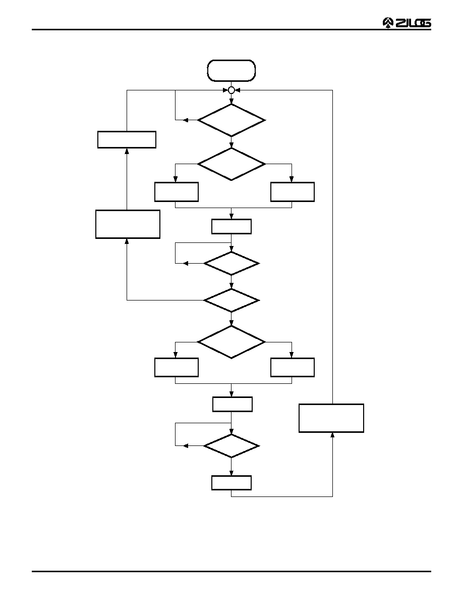
Z86E72/E73
OTP IR Microcontrollers
1-40
P R E L I M I N A R Y
DS96LVO1100
COUNTER/TIMER REGISTER DESCRIPTION (Continued)
Figure 30. Transmit Mode Flowchart
T8 (8-Bit)
Transmit Mode
T8_Enable Bit Set
CTR0, D7
No
Yes
T8_OUT Value
1
Load TC8L
Reset T8_OUT
Load TC8H
Set T8_OUT
Enable T8
Reset T8_Enable Bit
Set Time-out Status Bit
(CTR0 D5) and Generate
Timeout_Int If Enabled
No
T8_Timeout
Yes
Single Pass?
Modulo-N
T8_OUT Value
Load TC8L
Reset T8_OUT
Load TC8H
Set T8_OUT
Enable T8
No
T8_Timeout
Disable T8
Yes
Set Time-out Status Bit
(CTR0 D5) and Generate
Timeout_Int If Enabled
Single Pass
0
1
0

Z86E72/E73
OTP IR Microcontrollers
DS96LVO1100
P R E L I M I N A R Y
1-41
1
Figure 31. Demodulation Mode Flowchart
T8 (8-Bit)
Demodulation Mode
T8_Enable
CTR0, D7
No
Yes
Edge Present
No
T8_Enable Bit Set
Yes
Set Edge Present Status
Bit And Trigger Data
Capture Int. If Enabled
No
%FF
TC8
Yes
Enable TC8
Edge Present
Disable T8
Yes
T8 Time Out
Yes
Set Time-out Status
Bit And Trigger Time
Out Int. If Enabled
No
Continue Counting

Z86E72/E73
OTP IR Microcontrollers
1-42
P R E L I M I N A R Y
DS96LVO1100
COUNTER/TIMER REGISTER DESCRIPTION (Continued)
T16 Transmit Mode
In Normal or Ping-Pong Mode, the output of T16 when not
enabled is dependent on CTR1, D0. If it is a 0, T16_OUT
is a 1; if it is a 1, T16_OUT is 0. The user can force the out-
put of T16 to either a 0 or 1 whether it is enabled or not by
programming CTR1 D3, D2 to a 10 or 11.
When T16 is enabled, TC16H * 256 + TC16L is loaded,
and T16_OUT is switched to its initial value (CTR1 D0).
When T16 counts down to 0, T16_OUT is toggled (in Nor-
mal or Ping-Pong Mode), an interrupt is generated if en-
abled (CTR2 D1), and a status bit (CTR2 D5) is set. Note
that global interrupts will override this function as de-
scribed in the interrupts section. If T16 is in Single-Pass
Mode, it is stopped at this point. If it is in Modulo-N Mode,
it is loaded with TC16H * 256 + TC16L and the counting
continues.
The user can modify the values in TC16H and TC16L at
any time. The new values take effect when they are load-
ed. Care must be taken not to load these registers at the
time the values are to be loaded into the counter/timer, to
ensure known operation. An initial count of 1 is not al-
lowed. An initial count of 0 will cause T16 to count from 0
to %FF FF to %FFFE. Transition from 0 to %FFFF is not a
time-out condition.
Figure 32. 16-Bit Counter/Timer Circuits
Z8 Data Bus
Pos Edge
Neg Edge
CTR2 D2
IRQ3
CTR2 D1
T16_OUT
TC16L
TC16H
Clock
Select
SCLK
CTR2 D4, D3
Clock
16-Bit
Counter
T16
HI16
LO16
Z8 Data Bus
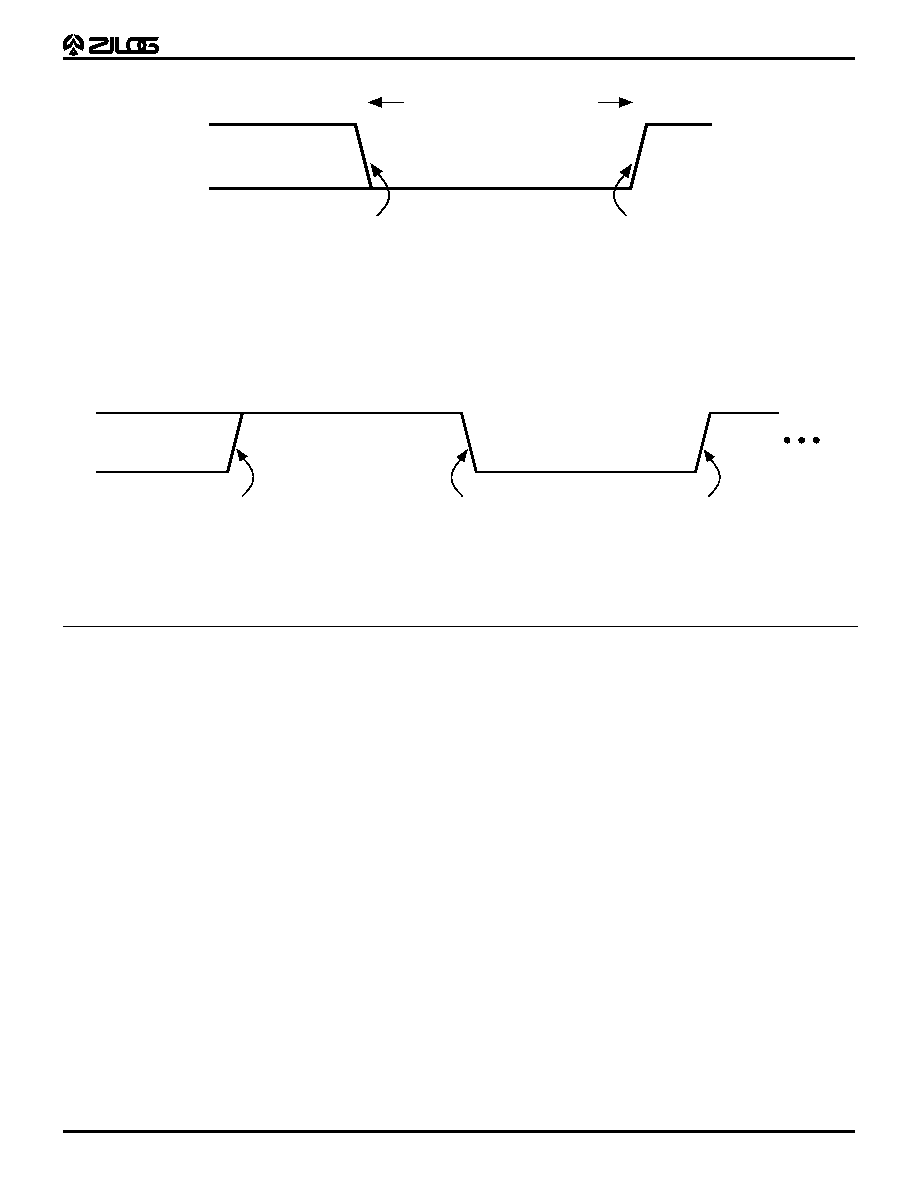
Z86E72/E73
OTP IR Microcontrollers
DS96LVO1100
P R E L I M I N A R Y
1-43
1
T16 Demodulation Mode
The user should program TC16L and TC16H to %FF. After
T16 is enabled, when the first edge (rising, falling or both
depending on CTR1, D5, D4) is detected. T16 captures
HI16 and LO16, reloads and begins counting.
If D6 of CTR2 is 0: When a subsequent edge (rising, fall-
ing, or both depending on CTR1 D5, D4) is detected during
counting, the current count in T16 is one's complemented
and put into HI16 and LO16. When data is captured, one
of the edge detect status bits (CTR1 D1, D0) is set and an
interrupt is generated if enabled (CTR2 D2). T16 is loaded
with %FFFF and starts again.
If D6 of CTR2 is 1: T16 ignores the subsequent edges in
the input signal and continues counting down. A time out
of T8 will cause T16 to capture its current value and gen-
erate an interrupt if enabled (CTR2, D2). In this case, T16
does not reload and continues counting. If D6 bit of CTR2
is toggled (by writing a 0 then a 1 to it), T16 will capture and
reload on the next edge (rising, falling, or both depending
on CTR1 D5, D4) but continue to ignore subsequent edg-
es.
Should T16 reach 0, it continues counting from %FFFF;
meanwhile, a status bit (CTR2 D5) is set and an interrupt
time-out can be generated if enabled (CTR2 D1).
Figure 33. T16_OUT in Single-Pass Mode
TC16H*256+TC16L Counts
"Counter Enable" Command,
T16_OUT Switches To Its
Initial Value (CTR1 D0)
T16_OUT Toggles,
Time-Out Interrupt
Figure 34. T16_OUT in Modulo-N Mode
TC16H*256+TC16L
"Counter Enable" Command,
T16_OUT Switches To Its
Initial Value (CTR1 D0)
T16_OUT Toggles,
Time-Out Interrupt
TC16H*256+TC16L
TC16H*256+TC16L
T16_OUT Toggles,
Time-Out Interrupt
T16_OUT

Z86E72/E73
OTP IR Microcontrollers
1-44
P R E L I M I N A R Y
DS96LVO1100
COUNTER/TIMER REGISTER DESCRIPTION (Continued)
Ping-Pong Mode
This operation mode is only valid in Transmit Mode. T8
and T16 need to be programmed in Single-Pass Mode
(CTR0 D6, CTR2 D6) and Ping-Pong Mode needs to be
programmed in CTR1 D3, D2. The user can begin the op-
eration by enabling either T8 or T16 (CTR0 D7 or CTR2
D7). For example, if T8 is enabled, T8_OUT is set to this
initial value (CTR1 D1). According to T8_OUT's level,
TC8H or TC8L is loaded into T8. After the terminal count
is reached, T8 is disabled and T16 is enabled. T16_OUT
switches to its initial value (CTR1 D0), data from TC16H
and TC16L is loaded, and T16 starts to count. After T16
reaches the terminal count it stops, T8 is enabled again,
and the whole cycle repeats. Interrupts can be allowed
when T8 or T16 reaches terminal control (CTR0 D1, CTR2
D1). To stop the Ping-Pong operation, write 00 to bits D3
and D2 of CTR1.
Note: Enabling Ping-Pong operation while the
counter/timers are running may cause intermittent
counter/timer function. Disable the counter/timers, then
reset the status flags prior to instituting this operation.
To Initiate Ping-Pong Mode
First, make sure both counter/timers are not running. Then
set T8 into Single-Pass Mode (CTR0 D6), set T16 into Sin-
gle-Pass Mode (CTR2 D6), and set Ping-Pong Mode
(CTR1 D2, D3). These instructions do not have to be in
any particular order. Finally, start Ping-Pong Mode by en-
abling either T8 (CTR0 D7) or T16 (CTR2 D7).
During Ping-Pong Mode
The enable bits of T8 and T16 (CTR0 D7, CTR2 D7) will
alternately be set and cleared by hardware. The time-out
bits (CTR0 D5, CTR2 D5) will be set every time the
counter/timers reach the terminal count.
Figure 35. Ping-Pong Mode
Enable
TC8
Time-Out
Enable
TC16
Time-Out
Ping-Pong
CTR1 D3,D2

Z86E72/E73
OTP IR Microcontrollers
DS96LVO1100
P R E L I M I N A R Y
1-45
1
Figure 36. Output Circuit
AND/OR/NOR/NAND
Logic
T8_OUT
CTR1 D5,D4
P34_INTERNAL
CTR0 D0
P36_INTERNAL
CTR1 D6
P35_INTERNAL
CTR2 D0
P35_EXT
P36_EXT
P34_EXT
MUX
MUX
MUX
T16_OUT
MUX
CTR1, D2
CTR1 D3

Z86E72/E73
OTP IR Microcontrollers
1-46
P R E L I M I N A R Y
DS96LVO1100
COUNTER/TIMER REGISTER DESCRIPTION (Continued)
Interrupts. The Z86E7X has five different interrupts. The
interrupts are maskable and prioritized (Figure 42). The
five sources are divided as follows: three sources are
claimed by Port 3 lines P33-P31, the remaining two by the
counter/timers (Table 10). The Interrupt Mask Register
globally or individually enables or disables the five inter-
rupt requests.
Figure 37. Interrupt Block Diagram
Interrupt
Edge
Select
IRQ Register (D6, D7)
IRQ 1, 3, 4
IRQ
IMR
IPR
Priority
Logic
5
Vector Select
IRQ0
IRQ2
Global
Interrupt
Enable
Interrupt
Request
Z86E72/E73
OTP IR Microcontrollers
DS96LVO1100
P R E L I M I N A R Y
1-47
1
When more than one interrupt is pending, priorities are re-
solved by a programmable priority encoder controlled by
the Interrupt Priority register. An interrupt machine cycle is
activated when an interrupt request is granted. This dis-
ables all subsequent interrupts, saves the Program
Counter and Status Flags, and then branches to the pro-
gram memory vector location reserved for that interrupt.
All Z86E7X interrupts are vectored through locations in the
program memory. This memory location and the next byte
contain the 16-bit address of the interrupt service routine
for that particular interrupt request. To accommodate
polled interrupt systems, interrupt inputs are masked and
the Interrupt Request register is polled to determine which
of the interrupt requests need service.
An interrupt resulting from AN1 is mapped into IRQ2, and
an interrupt from AN2 is mapped into IRQ0. Interrupts
IRQ2 and IRQ0 may be rising, falling, or both edge trig-
gered, and are programmable by the user. The software
can poll to identify the state of the pin.
Programming bits for the Interrupt Edge Select are located
in the IRQ Register (R250), bits D7 and D6 . The configu-
ration is shown in Table 11.
Clock. The Z86E7X on-chip oscillator has a high-gain,
parallel-resonant amplifier for connection to a crystal, LC,
ceramic resonator, or any suitable external clock source
(XTAL1 = Input, XTAL2 = Output). The crystal should be
AT cut, 1 MHz to 8 MHz maximum, with a series resistance
(RS) less than or equal to 100 Ohms. The Z86L7X on-chip
oscillator may be driven with a cost-effective RC network
or other suitable external clock source.
The crystal should be connected across XTAL1 and
XTAL2 using the recommended capacitors (capacitance
greater than or equal to 22 pF) from each pin to ground.
The RC oscillator configuration is an external resistor con-
nected from XTAL1 to XTAL2, with a frequency-setting ca-
pacitor from XTAL1 to ground (Figure 44).
Table 6. Interrupt Types, Sources, and Vectors
Name
Source
Vector
Location
Comments
IRQ0
/DAV0, IRQ0
0, 1
External
(P32), Rising
Falling Edge
Triggered
IRQ1,
IRQ1
2, 3
External
(P33), Falling
Edge
Triggered
IRQ2
/DAV2, IRQ2,
T
IN
4,5
External
(P31), Rising
Falling Edge
Triggered
IRQ3
T16
6, 7
Internal
IRQ4
T8
8, 9
Internal
Table 7. IRQ Register
IRQ
Interrupt Edge
D7
D6
IRQ2 (P31)
IRQ0 (P32)
0
0
1
1
0
1
0
1
F
F
F
R/F
F
R
F
R/F
Notes:
F = Falling Edge
R = Rising Edge
In analog mode, the Stop-Mode Recovery sources selected by
the SMR register are connected to the IRQ1 input. Any of the
Stop-Mode Recovery sources for SMR (except P31, P32, and
P33) can be used to generate IRQ1 (falling edge triggered).
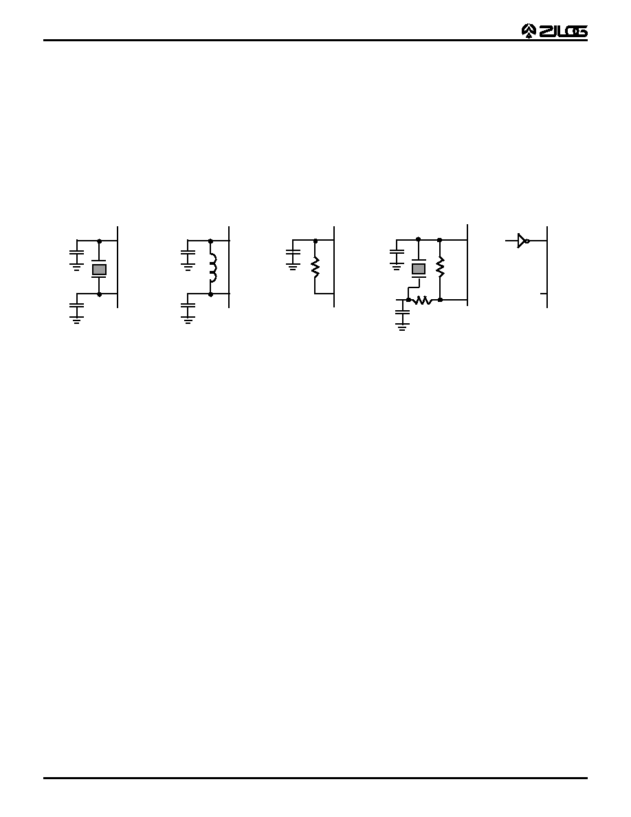
Z86E72/E73
OTP IR Microcontrollers
1-48
P R E L I M I N A R Y
DS96LVO1100
COUNTER/TIMER REGISTER DESCRIPTION (Continued)
Power-On Reset (POR). A timer circuit clocked by a ded-
icated on-board RC oscillator is used for the Power-On Re-
set (POR) timer function. The POR time allows VCC and
the oscillator circuit to stabilize before instruction execu-
tion begins.
The POR timer circuit is a one-shot timer triggered by one
of three conditions:
1.
Power Fail to Power OK status.
2.
Stop-Mode Recovery (if D5 of SMR = 1).
3.
WDT Time-Out.
The POR time is a nominal 5 ms. Bit 5 of the Stop-Mode
Register determines whether the POR timer is bypassed
after Stop-Mode Recovery (typical for external clock, RC,
LC oscillators).
Figure 38. Oscillator Configuration
XTAL1
XTAL2
C1
C2
C1
C2
C1
XTAL1
XTAL2
XTAL1
XTAL2
XTAL1
XTAL2
Ceramic Resonator or Crystal
C1, C2 = 47 pF TYP *
f = 8 MHz
LC
C1, C2 = 22 pF
L = 130
µ
H *
f = 3 MHz *
RC
@ 3V VCC (TYP)
C1 = 33 pF *
R = 1K *
External Clock
L
R
* Preliminary value including pin parasitics
C1
32 kHz XTAL
C1 = 20 pF, C = 33
pF
Rd = 56 - 470K
Rf =10 M
Rf
C2
Rd
XTAL1
XTAL2

Z86E72/E73
OTP IR Microcontrollers
DS96LVO1100
P R E L I M I N A R Y
1-49
1
HALT. HALT turns off the internal CPU clock, but not the
XTAL oscillation. The counter/timers and external inter-
rupts IRQ0, IRQ1, IRQ2, IRQ3, and IRQ4 remain active.
The devices are recovered by interrupts, either externally
or internally generated. An interrupt request must be exe-
cuted (enabled) to exit HALT mode. After the interrupt ser-
vice routine, the program continues from the instruction af-
ter the HALT.
STOP. This instruction turns off the internal clock and ex-
ternal crystal oscillation and reduces the standby current
to 10
µ
A (typical) or less. STOP mode is terminated only
by a reset, such as WDT time-out, POR, SMR, or external
reset. This causes the processor to restart the application
program at address 000CH. In order to enter STOP (or
HALT) mode, it is necessary to first flush the instruction
pipeline to avoid suspending execution in mid-instruction.
To do this, the user must execute a NOP (opcode = FFH)
immediately before the appropriate sleep instruction, i.e.,
FF
NOP
; clear the pipeline
6F
STOP
; enter STOP mode
or
FF
NOP
; clear the pipeline
7F
HALT
; enter HALT mode
Port Configuration Register (PCON). The PCON regis-
ter configures the comparator output on Port 3. It is locat-
ed in the expanded register file at Bank F, location 00 (Fig-
ure 44).
Comparator Output Port 3 (D0). Bit 0 controls the com-
parator used in Port 3. A 1 in this location brings the com-
parator outputs to P34 and P37, and a 0 releases the Port
to its standard I/O configuration.
Stop-Mode Recovery Register (SMR). This register se-
lects the clock divide value and determines the mode of
Stop-Mode Recovery (Figure 46). All bits are write only ex-
cept bit 7, which is read only. Bit 7 is a flag bit that is hard-
ware set on the condition of STOP recovery and reset by
a power-on cycle. Bit 6 controls whether a low level or a
high level is required from the recovery source. Bit 5 con-
trols the reset delay after recovery. Bits D2, D3, and D4, of
the SMR register, specify the source of the Stop-Mode Re-
covery signal. Bit D0 determines if SCLK/TCLK are divided
by 16 or not. The SMR is located in Bank F of the Expand-
ed Register Group at address 0BH
Figure 39. Port Configuration Register (PCON)
(Write Only)
Reserved (Must be 1)
D7
D6
D5
D4 D3
D2
D1
D0
PCON (0F) 0H
Comparator Output Port 3
0 P34, P37 Standard Output*
1 P34, P37 Comparator Output
* Default Setting After Reset
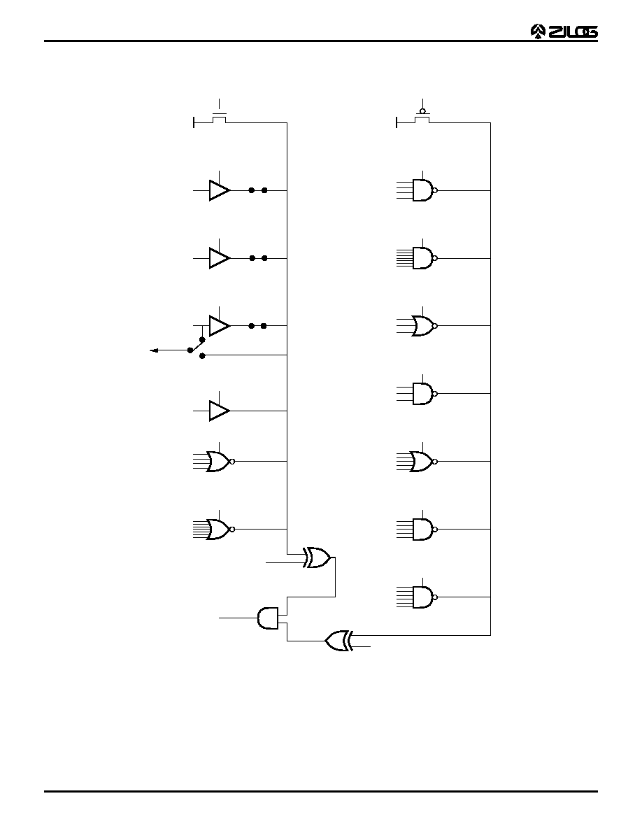
Z86E72/E73
OTP IR Microcontrollers
1-50
P R E L I M I N A R Y
DS96LVO1100
COUNTER/TIMER REGISTER DESCRIPTION (Continued)
Figure 40. Stop-Mode Recovery Register
P00
P32
VCC
P31
P32
P33
P27
P20
P23
P20
P27
SMR D4
0
D3
0
D2
0
SMR D4
0
D3
1
D2
0
SMR D4
0
D3
1
D2
1
SMR D4
1
D3
0
D2
0
SMR D4
1
D3
0
D2
1
SMR D4
1
D3
1
D2
0
SMR D4
1
D3
1
D2
1
SMR2 D4
0
D3
0
D2
0
SMR2 D4
0
D3
1
D2
0
SMR2 D4
0
D3
1
D2
1
SMR2 D4
1
D3
0
D2
0
SMR2 D4
1
D3
0
D2
1
SMR2 D4
1
D3
1
D2
0
SMR2 D4
1
D3
1
D2
1
SMR2 D4
0
D3
0
D2
1
VCC
P20
P32
P23
P20
P27
P31
P33
P31
P33
P32
P31
P33
P00
P07
P32
P31
P33
P07
P20
P32
P31
P33
P21
P22
SMR2 D6
SMR D6
To RESET and WDT
Circuitry (Active Low)
S1
S2
S3
S4
To IRQ1

Z86E72/E73
OTP IR Microcontrollers
DS96LVO1100
P R E L I M I N A R Y
1-51
1
SCLK/TCLK Divide-by-16 Select (D0). D0 of the SMR
controls a Divide-by-16 prescaler of SCLK/TCLK. The pur-
pose of this control is to selectively reduce device power
consumption during normal processor execution (SCLK
control) and/or HALT mode (where TCLK sources interrupt
logic). After Stop-Mode Recovery, this bit is set to a 0.
Stop-Mode Recovery Source (D2, D3, and D4). These
three bits of the SMR specify the wake up source of the
STOP recovery (Figure 49 and Table 12).
Note: Any Port 2 bit defined as an output will drive the cor-
responding input to the default state to allow the remaining
inputs to control the AND/OR function. Refer to SMR2 reg-
ister for other recover sources.
Stop-Mode Recovery Delay Select (D5). This bit, if low,
disables the 5 ms /RESET delay after Stop-Mode Recov-
ery. The default configuration of this bit is one. If the "fast"
wake up is selected, the Stop-Mode Recovery source
needs to be kept active for at least 5TpC.
Stop-Mode Recovery Edge Select (D6). A 1 in this bit po-
sition indicates that a High level on any one of the recovery
sources wakes the Z86E7X from STOP mode. A 0 indi-
cates Low level recovery. The default is 0 on POR (Figure
36).
Cold or Warm Start (D7). This bit is set by the device
upon entering STOP mode. It is a Read Only Flag bit. A 1
in D7 (warm) indicates that the device will awaken from a
SMR source or a WDT while in STOP mode. A 0 in this bit
(cold) indicates that the device will be reset by a POR or
WDT while not in STOP.
Stop-Mode Recovery Register 2 (SMR2). This register
determines the mode of STOP mode recovery for SMR2.
(Figure 49)
If SMR2 is used in conjunction with SMR, either of the
specified events will cause a Stop-Mode Recovery.
Note: Port pins configured as outputs are ignored as a
SMR or SMR2 recovery source. For example, if the NAND
of P23-P20 is selected as the recovery source and P20 is
configured as an output then the remaining SMR pins
(P23-P21) form the NAND equation.
Figure 41. SCLK Circuit
Table 8. Stop-Mode Recovery Source
SMR:432
Operation
D4
D3
D2
Description of Action
0
0
0
POR and/or external reset recovery
0
0
1
Reserved
P27 transition
Logical NOR of
P20 through P23
Logical NOR of
P20 through P27
0
1
0
0
1
1
1
0
0
1
0
1
1
1
0
1
1
1
SMR, D0
˜
2
˜
16
OSC
SCLK
TCLK
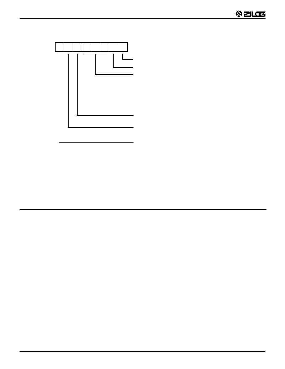
Z86E72/E73
OTP IR Microcontrollers
1-52
P R E L I M I N A R Y
DS96LVO1100
COUNTER/TIMER REGISTER DESCRIPTION (Continued)
Watch-Dog Timer Mode Register (WDTMR). The WDT
is a retriggerable one-shot timer that resets the Z8 if it
reaches its terminal count. The WDT must initially be en-
abled by executing the WDT instruction and refreshed on
subsequent executions of the WDT instruction. The WDT
circuit is driven by an on-board RC oscillator or external
oscillator from the XTAL1 pin. The WDT instruction affects
the Zero (Z), Sign (S), and Overflow (V) flags.
The POR clock source is selected with bit 4 of the WDT
register. Bit 0 and 1 control a tap circuit that determines the
time-out period. Bit 2 determines whether the WDT is ac-
tive during HALT and Bit 3 determines WDT activity during
STOP. Bits 5 through 7 are reserved (Figure 48).
This register is accessible only during the first 64 proces-
sor cycles (128 XTAL clocks) from the execution of the first
instruction after Power-On-Reset, Watch-Dog Reset, or a
Stop-Mode Recovery (Figure 40). After this point, the reg-
ister cannot be modified by any means, intentional or oth-
erwise. The WDTMR cannot be read and is located in
Bank F of the Expanded Register Group at address loca-
tion 0FH. It is organized as follows:
Figure 42. Stop-Mode Recovery Register 2
((0F) DH: D2-D4, D6 Write Only)
D7 D6
D5
D4
D3
D2
D1
D0
SMR2 (0F) DH
Reserved (Must be 0)
Reserved (Must be 0)
Stop-Mode Recovery Source 2
000 POR only*
001 NAND P20, P21, P22, P23
010 NAND P20, P21, P22, P23, P24, P25, P26, P27
011 NOR P31, P32, P33
100 NAND P31, P32, P33
101 NOR P31, P32, P33, P00, P07
110 NAND P31, P32, P33, P00, P07
111 NAND P31, P32, P33, P20, P21, P22
Reserved
(Must be 0)
Recovery Level
0 Low*
1 High
Reserved (Must be 0)
Note: If used in conjunction with SMR,
either of the two specified events will
cause a Stop-Mode Recovery.
*Default Setting After Reset

Z86E72/E73
OTP IR Microcontrollers
DS96LVO1100
P R E L I M I N A R Y
1-53
1
WDT Time Select (D0, D1). Selects the WDT time period.
It is configured as shown in Table 13.
WDTMR During HALT (D2). This bit determines whether
or not the WDT is active during HALT mode. A 1 indicates
active during HALT. The default is 1.
WDTMR During STOP (D3). This bit determines whether
or not the WDT is active during STOP mode. Since the
XTAL clock is stopped during STOP mode, the on-board
RC has to be selected as the clock source to the
WDT/POR counter. A 1 indicates active during STOP. The
default is 1.
Clock Source for WDT (D4). This bit determines which
oscillator source is used to clock the internal POR and
WDT counter chain. If the bit is a 1, the internal RC oscil-
lator is bypassed and the POR and WDT clock source is
driven from the external pin, XTAL1. The default configu-
ration of this bit is 0, which selects the RC oscillator.
Figure 43. Watch-Dog Timer Mode Register
(Write Only)
D7
D6
D5
D4
D3
D2
D1
D0
WDTMR (0F) FH
WDT TAP INT RC OSC External Clock
00 5 ms 256 TpC
01 10 ms 512 TpC
10 20 ms 1024 TpC
11 80 ms 4096 TpC
WDT During HALT
0 OFF
1 ON
WDT During STOP
0 OFF
1 ON
XTAL1/INT RC Select for WDT
0 On-Board RC
1 XTAL
Reserved (Must be 0)
* Default Setting After Reset
*
*
*
*
Table 9. WDT Time Select
D1
D0
Time-Out of
Internal RC
OSC
Time-Out of
XTAL Clock
0
0
5 ms min
256 TpC
0
1
10 ms mi
512 TpC
1
0
20 ms mi
1024 TpC
1
1
80 ms mi
4096 TpC
Notes:
TpC = XTAL clock cycle
The default on reset is 10 ms

Z86E72/E73
OTP IR Microcontrollers
1-54
P R E L I M I N A R Y
DS96LVO1100
COUNTER/TIMER REGISTER DESCRIPTION (Continued)
Figure 44. Resets and WDT
CLK
18 Clock RESET
Generator
RESET
* /CLR 2
WDT TAP SELECT
INTERNAL
RC
OSC.
CLK
*CLR1
POR
WDT1
2
3
4
Low Operating
Voltage Det.
Internal
RESET
Active
High
CK Source
Select
(WDTMR)
XTAL
VDD
VBO/VLV
2V REF.
From Stop
Mode
Recovery
Source
WDT
Stop Delay
Select (SMR)
12 ns Glitch Filter
+
-
5 Clock
Filter
WDT/POR Counter Chain
M
U
X
/RESET
* /CLR1 and /CLR2 enable the WDT/POR and
18 Clock Reset timers upon a Low to High input translation.
VCC

Z86E72/E73
OTP IR Microcontrollers
DS96LVO1100
P R E L I M I N A R Y
1-55
1
Low Voltage Protection. An on-board Voltage Compara-
tor checks that V
CC
is at the required level to ensure cor-
rect operation of the device. Reset is globally driven if V
CC
is below V
LV
(Low Voltage). The minimum operating volt-
age varies with the temperature and operating frequency,
while V
LV
varies with temperature only.
Software Selectable Options. There are four Software
Selectable Options to choose from which corresponds to
the ROM based parts mask options. Register (F0) EH OTP
byte is where these options are controlled; these options
are:
Note: The RC oscillator Xtal1/2 option is invoked during
OTP programming as a user-selectable item.
The Low Voltage trip voltage (V
LV
) is less than 3.0V under
the following conditions:
Maximum (V
LV
) Conditions:
T
A
= 0
∞
C, +70
∞
C Internal clock frequency equal to or less
than 8.0 MHz
Note: The internal clock frequency is one-half the external
clock frequency.
The device functions normally above 3.0V under all condi-
tions. The minimum functionality point below 3V is to be
defined. The V
LV
is a function of temperature and process
parameters.
Bit Name
Reg(0F)EH
Port 0 Pull-ups (lower nibble)
On/Off
Port 0 Pull-ups (upper nibble)
On/Off
Port 2 Pull-ups
On/Off
Mouse/Normal
M/N
Figure 45. Typical Z86E7X Low Voltage
vs Temperature at 8 MHz
0
15
25
35
45
55
T
B
D
VL
V
VLV
Temperature
Z86E72/E73
OTP IR Microcontrollers
1-56
P R E L I M I N A R Y
DS96LVO1100
EPROM PROGRAMMING
Table 10. Programming and Testmode
Device Pins
User/Test Mode
Device Pin #
User Modes
P33
V
PP
P32
EPM
Pref1
/CE
P31
/OE
P20
/PGM
Addr
V
CC
Port 1
CNFG
DATA
Test
ADDR
A0-A3
Note
EPROM Read
V
CC
V
H
V
IL
V
IL
V
IH
Addr
3.0V
Out
XX
Program
V
PP
V
CC
V
IL
V
IH
V
IL
Addr
6.0V
In
XX
Program Verify
V
PP
V
CC
V
IL
V
IL
V
IH
Addr
6.0V
Out
XX
RC Option
V
PP
V
CC
V
H
V
IH
V
IL
XX
6.0V
XX
XX
Margin Read
V
VA
V
H
V
IL
V
H
V
IH
Addr
6.0V
Out
00
1
Shadow Row Rd
V
CC
V
H
V
IL
V
IL
V
IH
COL
3.0V
Out
01
1
Shadow Row Prg
V
PP
V
H
V
IL
V
IH
V
IL
COL
6.0V
In
01
1
Shadow Row Ver
V
PP
V
H
V
IL
V
IL
V
IH
COL
6.0V
Out
01
1
Shadow Col Rd
V
CC
V
H
V
IL
V
IL
V
IH
ROW
3.0V
Out
02
1
Shadow Col Prg
V
PP
V
H
V
IL
V
IH
V
IL
ROW
6.0V
In
03
1
Shadow Col Ver
V
PP
V
H
V
IL
V
IL
V
IH
ROW
6.0V
Out
02
1
Page Prg 2 Byte
V
PP
V
H
V
IL
V
IH
V
IL
TBD
6.0V
In
04
1
Page Prg 4 Byte
V
PP
V
H
V
IL
V
IH
V
IL
TBD
6.0V
In
05
1
Page Prg 8 Byte
V
PP
V
H
V
IL
V
IH
V
IL
TBD
6.0V
In
06
1
Page Prg 16 Byte
V
PP
V
H
V
IL
V
IH
V
IL
TBD
6.0V
In
07
1
Notes:
1. All test modes are entered by first setting up the corresponding test
address and then latching the address by bringing the /OE to V
H
and then
to V
IL
, except for the margin read which requires /OE to be kept at V
H
.
V
VA
= Variable from V
CC
to V
PP
V
PP
= 12.5V
±
0.5V
V
H
= 12.5V
±
0. 5V
V
IH
= 3V
V
IL
= 0V
XX = Irrelevant
I
PP
during programming = 40 mA maximum
I
CC
during programming, verify, or read = 40 mA maximum.

Z86E72/E73
OTP IR Microcontrollers
DS96LVO1100
P R E L I M I N A R Y
1-57
1
Table 11. Timing of Programming Waveform
Parameters
Name
Min
Max
Units
1
Address Setup Time
2
µ
s
2
Data Setup Time
2
µ
s
3
V
PP
Setup Time
2
µ
s
4
V
CC
Setup Time
2
µ
s
5
Chip Enable Setup Time
2
µ
s
6
Program Pulse Width
0.95
µ
s
7
Data Hold Time
2
µ
s
8
/OE Setup Time
2
µ
s
9
Data Access Time
200
ns
10
Data Output Float Time
100
ns
11
Overprogram Pulse Width
2.85
ms
12
EPM Setup Time
2
µ
s
13
/PGM Setup Time
2
µ
s
14
Address to /OE Setup Time
2
µ
s
15
Option Program Pulse Width
78
ms
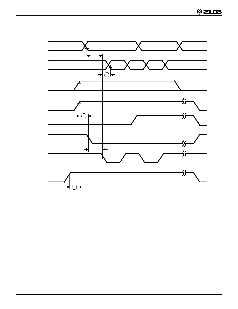
Z86E72/E73
OTP IR Microcontrollers
1-58
P R E L I M I N A R Y
DS96LVO1100
EPROM PROGRAMMING (Continued)
Figure 46. EPROM Read
Data
VIH
VIL
Invalid
Valid
Invalid
Valid
VIH
VIL
Address Stable
Address
Address Stable
0 Min
9
12
0 Min
EPM
VH
VIL
VCC
4.5V
/CE
VIH
VIL
/OE
VIH
VIL
VPP
VH
VIL
5.5V
/PGM
VIH
VIL
3
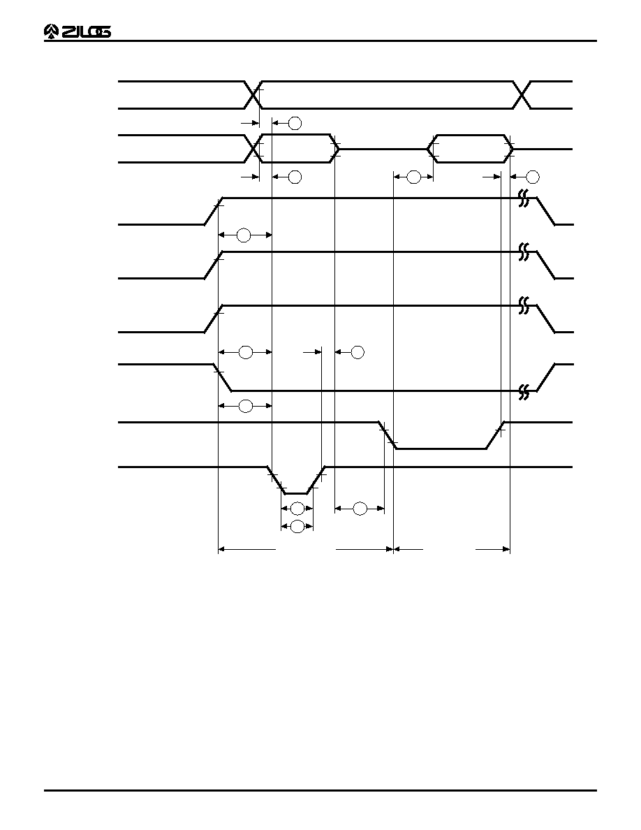
Z86E72/E73
OTP IR Microcontrollers
DS96LVO1100
P R E L I M I N A R Y
1-59
1
Figure 47. EPROM Program and Verify
Address
V
IH
V
IL
Address Stable
Data
V
IH
V
IL
Data Stable
Data Out Valid
1
2
10
9
3
V
PP
V
H
V
IH
EPM
V
IL
4
5
7
/CE
V
IL
6
8
11
/PGM
V
IH
V
IL
V
IH
V
H
VCC
4.5V
6V
/OE
V
IH
V
IL
Program Cycle
Verify Cycle

Z86E72/E73
OTP IR Microcontrollers
1-60
P R E L I M I N A R Y
DS96LVO1100
EPROM PROGRAMMING (Continued)
Figure 48. Programming EPROM, RAM Protect and 16K Size Selection
Address
V
IH
V
IL
Data
V
IH
V
IL
V
PP
V
IH
V
CC
6V
/OE
3
4
5
/CE
V
H
V
IH
/PGM
V
IH
V
IL
12
15
EPM
V
H
V
IL
EPROM Protect
RC Oscillator
4.5V
V
IH
V
IL
V
IH
V
IL
V
H
15
12
12
V
IL
V
IH
RAM Protect
15
Z86E72/E73
OTP IR Microcontrollers
DS96LVO1100
P R E L I M I N A R Y
1-61
1
Figure 49. Programming Flowchart
Start
Vcc = 6.0V
Vpp = 12.5V
N = 0
Program
1 ms Pulse
Increment N
N = 25 ?
Yes
No
Verify
One Byte
Pass
Fail
Prog. One Pulse
3xN ms Duration
Verify Byte
Fail
Pass
Increment
Address
Last Addr ?
Yes
No
Vcc = Vpp = 4.5V
Verify All
Bytes
Device Failed
Addr =
First Location
Fail
Pass
Vcc = Vpp = 5.5V
Verify All
Bytes
Device Passed
Pass
Fail
*
*
Note:
* To ensure proper operations during the spec.,
Zilog recommends verification over the Vcc
range of the device Vcc spec.
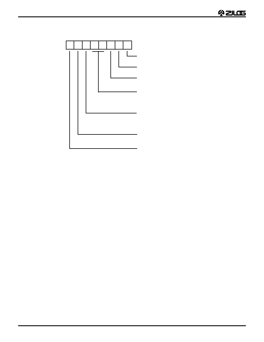
Z86E72/E73
OTP IR Microcontrollers
1-62
P R E L I M I N A R Y
DS96LVO1100
EXPANDED REGISTER FILE CONTROL REGISTERS (0D)
Figure 50. TC8 Control Register
((0D) 0H: Read/Write Except Where Noted)
D7
D6
D5
D4
D3
D2
D1
D0
CTR0 (0D) 0H
0 P34 as Port Output*
1 Timer8 Output
0 Disable T8 Time Out Interrupt
1 Enable T8 Time Out Interrupt
0 Disable T8 Data Capture Interrupt
1 Enable T8 Data Capture Interrupt
00 SCLK on T8
01 SCLK/2 on T8
10 SCLK/4 on T8
11 SCLK/8 on T8
R 0 No T8 Counter Time Out
R 1 T8 Counter Time Out Occured
W 0 No Effect
W 1 Reset Flag to 0
* Default Setting After Reset
0 Modulo-N
1 Single Pass
R 0 T8 Disabled *
R 1 T8 Enabled
W 0 Stop T8
W 1 Enable T8
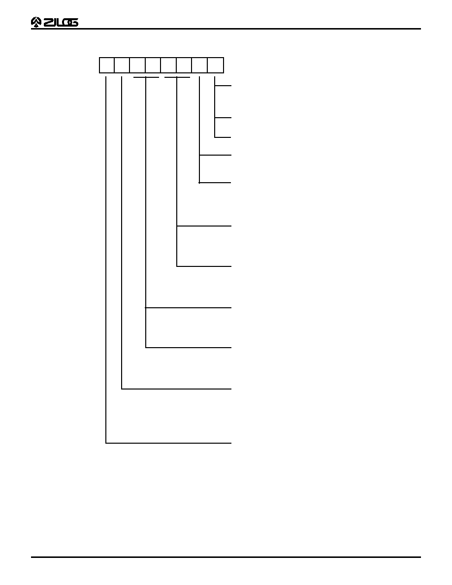
Z86E72/E73
OTP IR Microcontrollers
DS96LVO1100
P R E L I M I N A R Y
1-63
1
Figure 51. T8 and T16 Common Control Functions
((0D) 1H: Read/Write)
D7
D6
D5
D4
D3
D2
D1
D0
CTR1 (0D) 1H
0 T16_OUT is 0 Initially
1 T16_OUT is 1 Initially
R/W
R
R
W
W
0 No Falling Edge Detection
1 Falling Edge Detection
0 No Effect
1 Reset Flag to 0
0 T8_OUT is 0 Initially
1 T8_OUT is 1 Initially
0 No Rising Edge Detection
1 Rising Edge Detection
0 0 Normal Operation
0 1 Ping-Pong Mode
1 0 T16_OUT = 0
1 1 T16_OUT = 1
Transmit Mode/T8/T16 Logic
0 0 Falling Edge Detection
0 1 Rising Edge Detection
1 0 Both Edge Detection
1 1 Reserved
0 P36 as Port Output*
1 P36 as T8/T16_OUT
0 Transmit Mode*
1 Demodulation Mode
0 0 No Filter
0 1 4 SCLK Cycle Filter
1 0 8 SCLK Cycle Filter
1 1 16 SCLK Cycle Filter
Demodulation Mode
Transmit Mode
Transmit Mode
R/W
Demodulation Mode
R
R
W
W
Transmit Mode
Demodulation Mode
0 0 AND
0 1 OR
1 0 NOR
1 1 NAND
Demodulation Mode
Transmit Mode
0 P31 as Demodulator Input
1 P20 as Demodulator Input
Demodulation Mode
Transmit/Demodulation Modes
0 No Effect
1 Reset Flag to 0
Note: Care must be taken in differentiating
Transmit Mode from Demodulation Mode.
Depending on which of these two modes is
operating, the CTR1 bit will have different
functions.
*Note: Changing from one mode to
another cannot be done without
disabling the counter/timers.
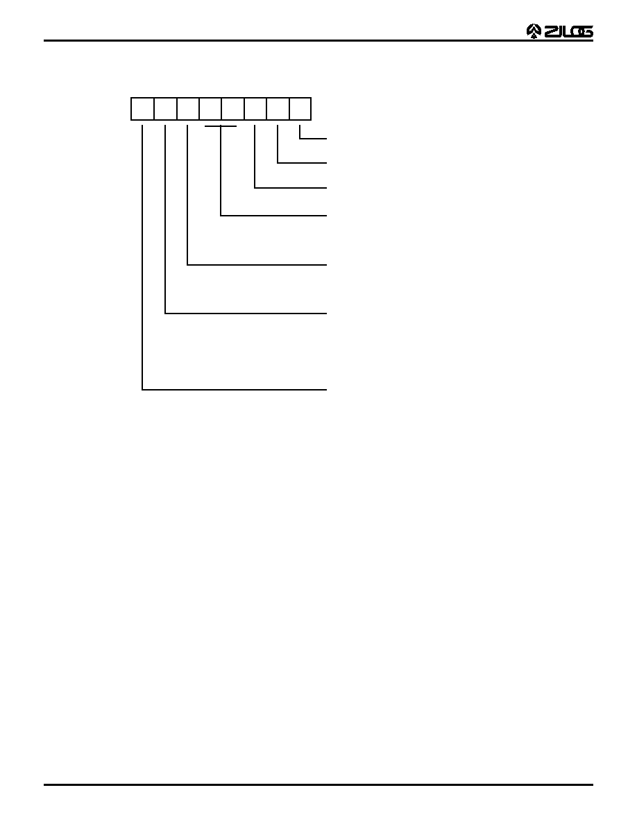
Z86E72/E73
OTP IR Microcontrollers
1-64
P R E L I M I N A R Y
DS96LVO1100
EXPANDED REGISTER FILE CONTROL REGISTERS (0D) (Continued)
Figure 52. T16 Control Register
((0D) 2H: Read/Write Except Where Noted)
D7 D6
D5
D4
D3
D2
D1
D0
CTR2 (0D) 02H
0 P35 is Port Output*
1 P35 is TC16 Output
0 Disable T16 Time-Out Interrupt
1 Enable T16 Time-Out Interrupt
0 0 SCLK on T16
0 1 SCLK/2 on T16
1 0 SCLK/4 on T16
1 1 SCLK/8 on T16
* Default Setting After Reset
0 Disable T16 Data Capture Interrupt
1 Enable T16 Data Capture Interrupt
R 0 No T16 Time Out
R 1 T16 Time Out Occurs
W 0 No Effect
W 1 Reset Flag to 0
0 Modulo-N for T16
1 Single Pass for T16
R 0 T16 Disabled *
R 1 T16 Enabled
W 0 Stop T16
W 1 Enable T16
Transmit Mode
0 T16 Recognizes Edge
1 T16 Does Not Recognize Edge
Demodulator Mode

Z86E72/E73
OTP IR Microcontrollers
DS96LVO1100
P R E L I M I N A R Y
1-65
1
EXPANDED REGISTER FILE CONTROL REGISTERS (0F)
Figure 53. Stop-Mode Recovery Register
((F) 0BH: D6-D0 = Write Only, D7 = Read Only)
D7
D6
D5
D4
D3
D2
D1
D0
SMR (0F) 0B
SCLK/TCLK Divide-by-16
0 OFF
1 ON
Reserved (Must be 0)
Stop-Mode Recovery Source
000
001
010
0 11
100
101
11 0
111
Stop Delay
0 OFF
1 ON
Stop Recovery Level
0 Low
1 High
Stop Flag
0 POR
1 Stop Recovery**
* Default Setting After Reset
** Default Setting After Reset and Stop-Mode Recovery
**
*
*
*
*
POR Only
Reserved
P31
P32
P33
P27
P2 NOR 0-3
P2 NOR 0-7

Z86E72/E73
OTP IR Microcontrollers
1-66
P R E L I M I N A R Y
DS96LVO1100
Figure 54. Stop-Mode Recovery Register 2
((0F) DH: D2-D4, D6 Write Only)
D7 D6
D5
D4
D3
D2
D1
D0
SMR2 (0F) DH
Reserved (Must be 0)
Reserved (Must be 0)
Stop-Mode Recovery Source 2
000 POR only*
001 NAND P20, P21, P22, P23
010 NAND P20, P21, P22, P23, P24, P25, P26, P27
011 NOR P31, P32, P33
100 NAND P31, P32, P33
101 NOR P31, P32, P33, P00, P07
110 NAND P31, P32, P33, P00, P07
111 NAND P31, P32, P33, P20, P21, P22
Reserved
(Must be 0)
Recovery Level
0 Low*
1 High
Reserved (Must be 0)
Note: If used in conjunction with SMR,
either of the two specified events will
cause a Stop-Mode Recovery.
*Default Setting After Reset
Figure 55. Option Bit Register
D7
D6
D5
D4
D3
D2
D1
D0
OPT (0F) EH
Port 0 (0-3) Pull-up
1 pull-up active
0 pull-up inactive
Port 0 (7-4) Pull-up
1 pull-up active
2 pull-up inactive
Port 2 pull-up option
1 pull-up active
0 pull-up inactive
Reserved (Must be 0.)
Mask option for
mouse trackball interface
P00-P03
1 For mouse trackball interface
0 Normal
Reserved (Must be 0)
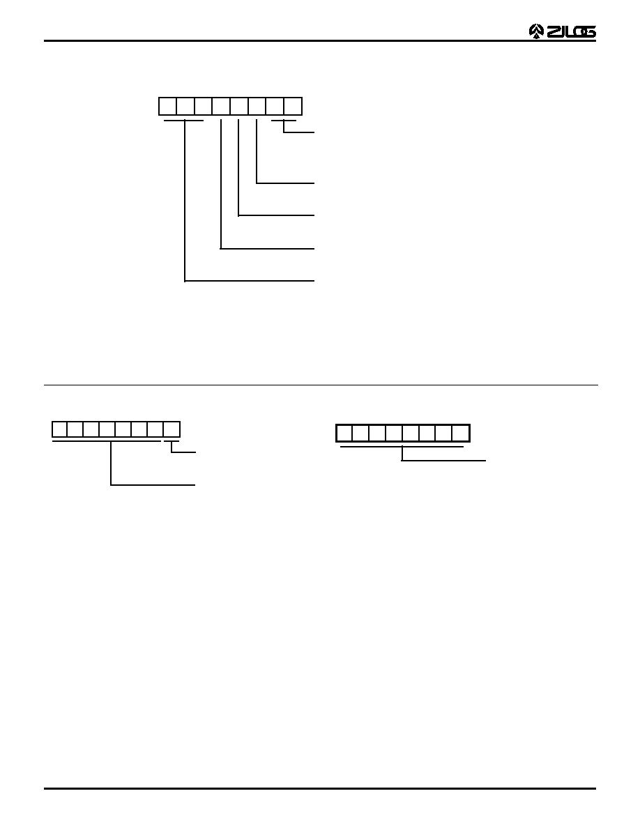
Z86E72/E73
OTP IR Microcontrollers
1-67
P R E L I M I N A R Y
DS96LVO1100
EXPANDED REGISTER FILE CONTROL REGISTERS (0F) (Continued)
Figure 56. Watch-Dog Timer Mode Register
((F) 0FH: Write Only)
D7
D6
D5
D4
D3
D2
D1
D0
WDTMR (0F) FH
WDT TAP INT RC OSC External Clock
00 5 ms 256 TpC
01 10 ms 512 TpC
10 20 ms 1024 TpC
11 80 ms 4096 TpC
WDT During HALT
0 OFF
1 ON
WDT During STOP
0 OFF
1 ON
XTAL1/INT RC Select for WDT
0 On-Board RC
1 XTAL
Reserved (Must be 0)
* Default Setting After Reset
*
*
*
*
Figure 57. Port Configuration Register (PCON)
((0F) 0H: Write Only)
Reserved (Must be 1)
D7
D6
D5
D4 D3
D2
D1
D0
PCON (0F) 0H
Comparator Output Port 3
0 P34, P37 Standard Output*
1 P34, P37 Comparator Output
* Default Setting After Reset
P37 comparator output only on E72
Figure 58. Port 2 Mode Register
(F6H: Write Only)
D7
D6
D5
D4
D3
D2
D1
D0
P27-P20 I/O Definition
0 Defines Bit as OUTPUT
1 Defines Bit as INPUT*
R246 P2M
*Default Setting After Reset

Z86E72/E73
OTP IR Microcontrollers
1-68
P R E L I M I N A R Y
DS96LVO1100
Z8
Æ
STANDARD CONTROL REGISTER DIAGRAMS
Figure 59. Port 3 Mode Register
(F7H: Write Only)
D7
D6
D5
D4
D3
D2
D1
D0
R247 P3M
0 Port 2 Open Drain*
1 Port 2 Push-pull
0 Parity Off
1 Parity On
0 P32 = Input
P35 = Output *
1 P32 = /DAV0/RDY0
P35 = RDY0//DAV0
0 P31 = Input (TIN)
P36 = Output (TOUT)
1 P31 = /DAV2/RDY2
P36 = RDY2//DAV2
0 P30 = Input
P37 = Output
1 P30 = Serial In
P37 = Serial Out
0 = P31, P32 Digital Mode
1 = P31, P32 Analog Mode
* Default Setting After Reset
00 P33 = Input
P34 = Output *
01 P33 = Input
10 P34 = /DM
P33 = /DAV1/RDY1
P34 = RDY1//DAV1
11
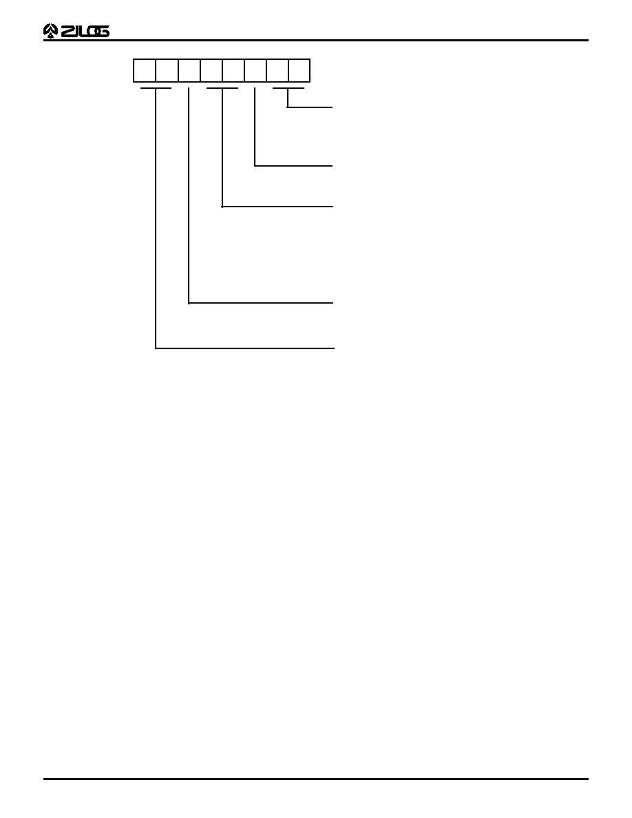
Z86E72/E73
OTP IR Microcontrollers
DS96LVO1100
P R E L I M I N A R Y
1-69
1
Figure 60. Port 0 and 1 Mode Register
(F8H: Write Only)
D7
D6
D5
D4
D3
D2
D1
D0
R248 P01M
P00-P03 Mode
00 Output
01 Input*
1X A11-A8
Stack Selection
0 External
1 Internal*
P17-P10 Mode
00 Byte Output
01 Reserved
10 AD7-AD0
11 High-Impedance AD7AD0,
/AS, /DS, /R//W, A11-A8,
A15-A12, If Selected
P07-P04 Mode
00 Output
01 Input*
1X A15-A12
External Memory Timing
0 Normal*
1 Extended
* Default Setting After Reset.
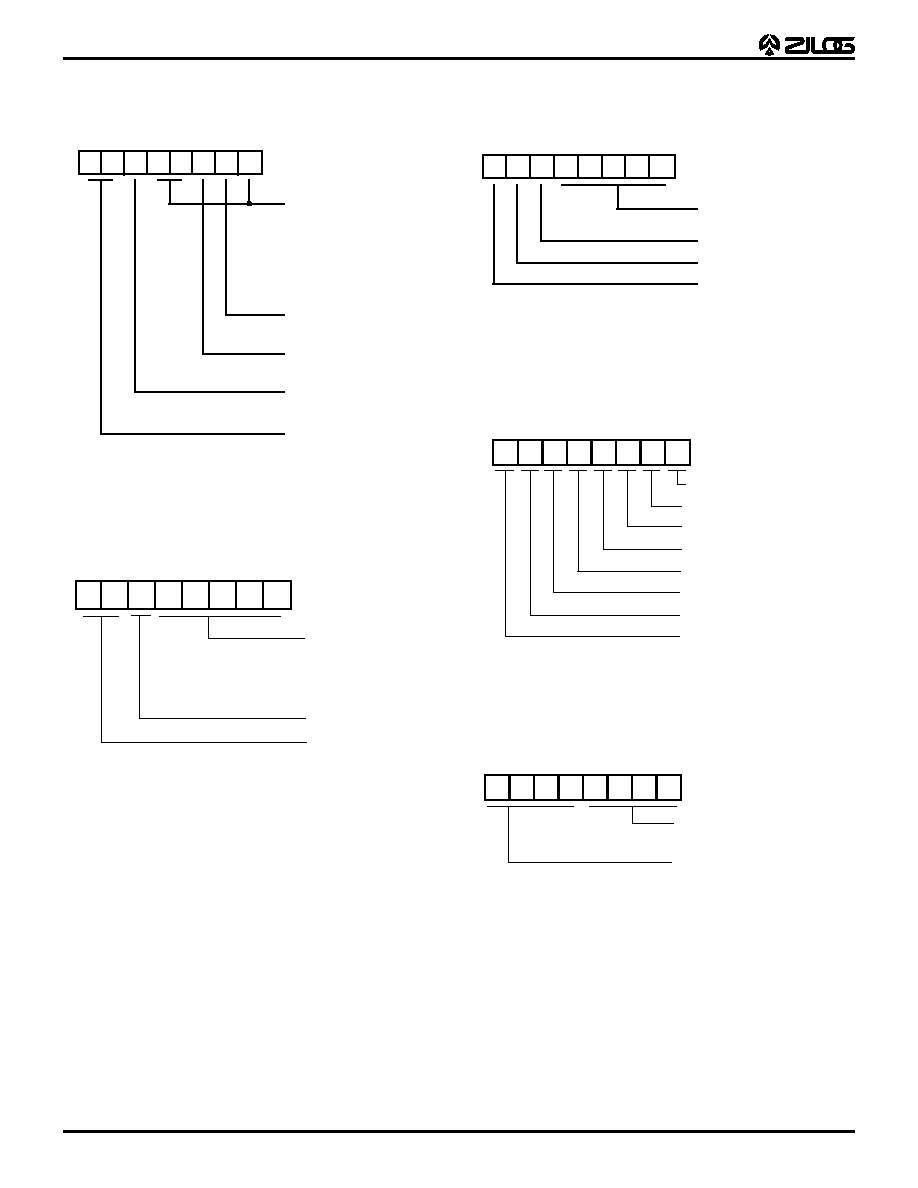
Z86E72/E73
OTP IR Microcontrollers
1-70
P R E L I M I N A R Y
DS96LVO1100
Z8
Æ
STANDARD CONTROL REGISTER DIAGRAMS (Continued)
Figure 61. Interrupt Priority Registers
((0) F9H: Write Only)
Figure 62. Interrupt Request Register
((0) FAH: Read/Write)
D7
D6
D5
D4
D3
D2
D1
D0
Interrupt Group Priority
000 Reserved
001 C > A > B
010 A > B > C
011 A > C > B
100 B > C > A
101 C > B > A
110 B > A > C
111 Reserved
IRQ3, IRQ5 Priority (Group A)
0 IRQ5 > IRQ3
1 IRQ3 > IRQ5
IRQ0, IRQ2 Priority (Group B)
0 IRQ2 > IRQ0
1 IRQ0 > IRQ2
IRQ1, IRQ4 Priority (Group C)
0 IRQ1 > IRQ4
1 IRQ4 > IRQ1
Reserved (Must be 0)
R249 IPR
D7
D6
D5
D4
D3
D2
D1
D0
R250 IRQ
Inter Edge
P31
P32
= 00
P31
P32
= 01
P31
P32
= 10
P31
P32
= 11
IRQ0 = P32 Input
IRQ1 = P33 Input
IRQ2 = P31 Input
IRQ3 = T16
IRQ4 = T8
Reserved (Must be 0)
Default Setting After Reset = 0000 0000
Figure 63. Interrupt Mask Register
((0) FBH: Read/Write)
Figure 64. Flag Register
((0) FCH: Read/Write
Figure 65. Register Pointer
((0) FDH: Read/Write)
D7 D6
D5
D4
D3
D2
D1
D0
Reserved (Must be 0)
1 Enables IRQ4-IRQ0
(D0 = IRQ0)
0 Master Interrupt Disable*
1 Master Interrupt Enable
R251 IMR
* Default Setting After Reset
Reserved (Must be 0)
D7 D6 D5 D4 D3 D2 D1 D0
User Flag F1
User Flag F2
Half Carry Flag
Decimal Adjust Flag
Overflow Tag
Sign Flag
Zero Flag
Carry Flag
R252 Flags
D7 D6 D5 D4 D3 D2 D1 D0
Expanded Register (Bank)
Pointer
Working Register
Pointer
R253 RP
Default Setting After
Reset = 0000

Z86E72/E73
OTP IR Microcontrollers
DS96LVO1100
P R E L I M I N A R Y
1-71
1
Figure 66. Stack Pointer High
((0) FEH: Read/Write)
D7 D6 D5 D4 D3 D2 D1 D0
Stack Pointer Upper
Byte (SP15-SP8)
R254 SPH
Figure 67. Stack Pointer Low
((0) FFH: Read/Write)
D7 D6 D5 D4 D3 D2 D1 D0
Stack Pointer Lower
Byte (SP7-SP0)
R255 SPL
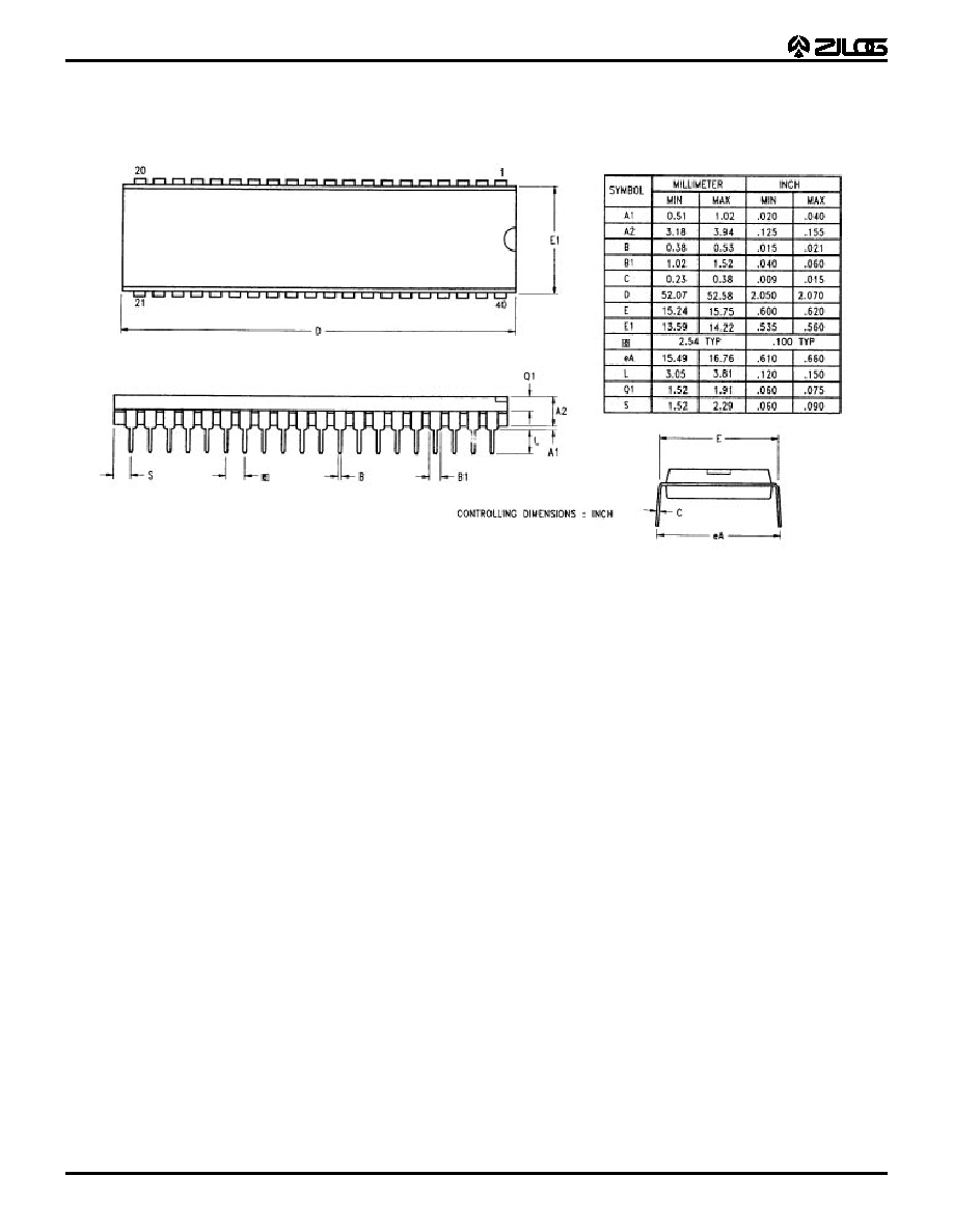
Z86E72/E73
OTP IR Microcontrollers
1-72
P R E L I M I N A R Y
DS96LVO1100
PACKAGE INFORMATION
Figure 68. 40-Pin DIP Package Diagram

Z86E72/E73
OTP IR Microcontrollers
DS96LVO1100
P R E L I M I N A R Y
1-73
1
Figure 69. 44-Pin QFP Package Diagram
Figure 70. 44-Pin PLCC Package Diagram

Z86E72/E73
OTP IR Microcontrollers
1-74
P R E L I M I N A R Y
DS96LVO1100
ORDERING INFORMATION
For fast results, contact your local Zilog sales office for assistance in ordering the part desired.
Package
P = Plastic DIP
F = Plastic Quad Flat Pack
V = Plastic Chip Carrier
Temperature
S = 0
∞
C to +70
∞
C
Speed
16 = 16 MHz
Environmental
C = Plastic Standard
Z86E72/E73
16 MHz
40-Pin DIP
44-Pin PLCC
44-Pin QFP
Z86E7216PSC
Z86E7216VSC
Z86E7216FSC
Z86E7316PSC
Z86E7316VSC
Z86E7316FSC
Example:
Z 86E73 16 P S C
Environmental Flow
Temperature
Package
Speed
Product Number
Zilog Prefix
is an Z86E73, 16 MHz, DIP, 0
∞
C to +70
∞
C, Plastic Standard Flow