 | –≠–ª–µ–∫—Ç—Ä–æ–Ω–Ω—ã–π –∫–æ–º–ø–æ–Ω–µ–Ω—Ç: Z86K15 | –°–∫–∞—á–∞—Ç—å:  PDF PDF  ZIP ZIP |

DS97KEY0204
P R E L I M I N A R Y
1
1
P
RELIMINARY
C
USTOMER
P
ROCUREMENT
S
PECIFICATION
Z86K13/K14/K15
K16/K17/K18
1
CMOS Z8
Æ
8-B
IT
MCU
K
EYBOARD
C
ONTROLLERS
FEATURES
s
4.5V to 5.5 V Operating Range
s
0
∞
C to +70
∞
C Operating Temperature Range
s
188 Bytes of Ram
s
Low-Power Consumption: 60 mW @ 5 MHz
s
Five Vectored, Priority Interrupts from FIve Different
Sources
s
A Programmable 8-Bit Counter/Timer, with 6-Bit
Programmable Prescaler
s
Power-On-Reset (POR) Timer, Hardware Watch-Dog
Timer (WDT)
s
Digital Inputs CMOS Levels with Internal Pull-Up
Resistors
s
Four Direct Connect LED Drive Ports
s
On-Chip RC Oscillator (Z86K13/14/15)
s
On-Chip Oscillator that Accepts a Crystal, Ceramic
Resonator, LC, or External Clock Drive (Z86K16/17/18)
s
Low System EMI Emission
GENERAL DESCRIPTION
The Z86KXX Keyboard Controllers are full-featured mem-
bers of the Z8
Æ
MCU family offering a unique register-to-
register architecture that avoids accumulator bottlenecks
and is more code efficient than RISC processors.
For keyboard applications demanding powerful I/O capa-
bilities, the Z86KXX provides 32 pins dedicated to input
and output for row, column, clock, data, and LEDs.
The on-chip counter/timer is available to relieve the system
of administering real-time tasks.
Five different internal or external interrupt sources are
maskable and prioritized in which a vectored address is
provided for efficient interrupt subroutine handling and
multitasking functions.
The Z86K15 achieves low EMI by means of several modi-
fications in the output drivers and clock circuitry of the de-
vice.
ROM
I/O
Speed
Pin Count/
Device
(KB)
Lines
(MHz)
Package
Z86K13
2
32
4-5
40-DIP, 44-PLCC,
44-QFP, COB
Z86K14
3
32
4-5
40-DIP, 44-PLCC,
44-QFP, COB
Z86K15
4
32
4-5
40-DIP, 44-PLCC,
44-QFP, COB
Z86K16
2
32
4-5
40-DIP, 44-PLCC,
44-QFP, COB
Z86K17
3
32
4-5
40-DIP, 44-PLCC,
44-QFP, COB
Z86K18
4
32
4-5
40-DIP, 44-PLCC,
44-QFP, COB
Z86K13/K14/K15/K16/K17/K18
CMOS Z8Æ 8-Bit MCU Keyboard Controllers
Zilog
2
P R E L I M I N A R Y
DS97KEY0204
GENERAL DESCRIPTION
(Continued)
Notes:
All signals with a preceding front slash, "/", are
active Low. For example, B//W (WORD is active Low);
/B/W (BYTE is active Low, only). Power connections follow
conventional descriptions below:
Connection
Circuit
Device
Power
V
CC
V
DD
Ground
GND
V
SS
Figure 1. Z86KXX Functional Block Diagram
Port 3
Interrupt
Control
Port 2
I/O
(Bit Programmable)
ALU
Flags
Register
Pointer
Machine
Timing & Inst.
Control
Program
Counter
GND
XT
AL1
XT
AL2
Output Input
Port 0
Port 1
Open-Drain
Output
Open-Drain
Output
WDT
POR
Input
4
4
4
8
8
Counter/
Timers
USB SIE
and Trans
Register File
208 x 8-Bytes
Program
Memory
4 KB ROM
VCC
D+
D-
3.3 V
VR
VCC

Z86K13/K14/K15/K16/K17/K18
Zilog
CMOS Z8Æ 8-Bit MCU Keyboard Controllers
DS97KEY0204
P R E L I M I N A R Y
3
1
PIN DESCRIPTION
Figure 2. 40-Pin DIP Configuration
P30
P31
P32
P33
*NC
*NC
P27
P26
P25
P24
GND
VCC
P00
P01
P02
P03
P04
P05
P06
P07
P23
P22
P21
P20
P37
P36
P35
P34
RCIN/XTAL1
AGND/XTAL2
GND
VCC
P17
P16
P15
P14
P13
P12
P11
P10
40
Z86KXX
DIP
1
20
21
Notes:
*Pin 5 and 6 used for testing Ground during normal operation.
When Pin 5 is connected to V
CC
. Pin 6 is CLK OUT.
When Pin 5 is connected to GND, Pin 6 outputs nothing.
These pins must be tied to ground in application.
Table 1. 40-Pin DIP Pin Identification
Pin #
Symbol
Function
Direction
1-4
P30-P33
Port 3, Pins 0,1,2,3
Input
5-6
NC
Tied to GND
7-10
P27-P24
Port 2, Pins 7,6,5,4
In/Output
11
GND
Ground
12
V
CC
Power Supply
Input
13-20
P00-P07
Port 0, Pins 0,1,2,3,4,5,6,7
Output
21-28
P10-P17
Port 1, Pins 0,1,2,3,4,5,6,7
Output
29
V
CC
Power Supply
30
GND
Ground
31
AGND/XTAL2
Analog Ground or Crystal Clock Out
32
RCIN/XTAL1
RCIN/Crystal Oscillator Clock
Input
33-36
P34-P37
Port 3, Pins 4,5,6,7
Output
37-40
P20-P23
Port 2, Pins 0,1,2,3
Input

Z86K13/K14/K15/K16/K17/K18
CMOS Z8Æ 8-Bit MCU Keyboard Controllers
Zilog
4
P R E L I M I N A R Y
DS97KEY0204
PIN DESCRIPTION
(Continued)
Figure 3. 44-Pin PLCC Pin Assignments
Z86KXX
PLCC
7
17
NC
P27
P26
P25
P24
GND
VCC
P00
P01
P02
P03
NC
P36
P35
P34
RCIN/XTAL1
NC
AGND/XTAL2
GND
VCC
P17
NC
P04
P05
P06
P07
P10
P11
P12
P13
P14
P15
P16
NC
NC
P33
P32
P31
P30
P23
P22
P21
P20
P37
1
28
18
40
39
29
6
Notes:
Pins 5 and 6 used for testing. Ground during normal operation
When Pin 43 is connected to V
CC
, Pin 44 is CLKOUT.
When Pin 43 is connected to GND. Pin 44 outputs nothing.
Table 2. 44-Pin PLCC Pin Assignments
Pin #
Symbol
Function
Direction
1-4
P30-P33
Port 3, Pins
0,1,2,3
Input
5-7
NC
Test Pins (GND)
8-11
P27-P24
Port 2, Pins
4,5,6,7
In/Output
12
GND
Ground
13
V
CC
Power Supply
14-21
P00-P07
Port 0, Pins
0,1,2,3,4,5,6,7
Output
22-28
P10-P16
Port 1, Pins
0,1,2,3,4,5,6
Output
29
NC
Not Connected
30
P17
Port 1, Pin 7
Output
31
V
CC
Power Supply
32
GND
Ground
33
AGND/ XTAL2 Analog Ground
or Crystal Clock
Out
34
NC
Not Connected
35
RCIN/ XTAL1
RCIN/Crystal
Oscillator Clock
Input
36-38
P34-P37
Port 3, Pins
4,5,6,7
Output
39
NC
Not Connected
40
P37
Port 3, Pin 7
Output
41-44
P20-P23
Port 2, Pins
0,1,2,3
In/Output
Table 2. 44-Pin PLCC Pin Assignments
Pin #
Symbol
Function
Direction
Z86K13/K14/K15/K16/K17/K18
Zilog
CMOS Z8Æ 8-Bit MCU Keyboard Controllers
DS97KEY0204
P R E L I M I N A R Y
5
1
Figure 4. 44-Pin QFP Pin Assignments
34
44
P37
P20
P21
P22
P23
P30
P31
P32
P33
NC
NC
P16
P15
P14
P13
P12
P11
P10
P07
P06
P05
P04
NC
P27
P26
P25
P24
GND
VCC
P00
P01
P02
P03
NC
P36
P35
P34
RCIN/XT
AL1
NC
A
GND/XT
AL2
GND
VCC
P17
NC
1
23
33
Z86KXX
QFP
11
22
12
Notes:
Pins 43 and 44 are used for testing ground during normal operation.
When Pin 45 is connected to V
CC
, Pin 46 is CLKOUT.
When Pin 45 is connected to GND. Pin 46 outputs nothing.
Table 3. 44-Pin QFP Pin Identification
Pin #
Symbol
Function
Direction
1
NC
Not Connected
2-5
P24-P27
Port 2, Pins
4,5,6,7
In/Output
6
GND
Ground
7
V
CC
Supply Voltage
8-15
P00-P07
Port 0, Pins
0,1,2,3,4,5,6,7,
Output
16-22
P10-P16
Port 1, Pins
0,1,2,3,4,5,6
Output
23
NC
Not Connected
24
P17
Port 1, Pin 7
Output
25
V
CC
Supply Voltage
26
GND
Ground
27
AGND/ XTAL2 Analog Ground/
Crystal Clock Out
28
NC
Not Connected
29
RCIN / XTAL1 RCIN/Crystal
Oscillator Clock
Input
30-32
P34-P36
Port 3, Pins 4,5,6 Output
33
NC
Not Connected
34
P37
Port 3, Pin 7
Output
35-38
P20-P23
Port 2, Pins
0,1,2,3
Input
39-42
P30-P33
Port 3, Pins
0,1,2,3
Input
43-44
NC
Test Pins (GND)
Table 3. 44-Pin QFP Pin Identification
Pin #
Symbol
Function
Direction

Z86K13/K14/K15/K16/K17/K18
CMOS Z8Æ 8-Bit MCU Keyboard Controllers
Zilog
6
P R E L I M I N A R Y
DS97KEY0204
ABSOLUTE MAXIMUM RATINGS
Stresses greater than those listed under Absolute Maxi-
mum Ratings may cause permanent damage to the de-
vice. This is a stress rating only; operation of the device at
any condition above those indicated in the operational sec-
tions of these specifications is not implied. Exposure to ab-
solute maximum rating conditions for extended periods
may affect device reliability.
STANDARD TEST CONDITIONS
The characteristics listed here apply for standard test con-
ditions as noted. All voltages are referenced to GND. Pos-
itive current flows into the referenced pin (Figure 5).
CAPACITANCE
T
A
= 25
∞
C; V
CC
= GND = 0V; f = 1.0 MHz; unmeasured pins returned to GND.
Frequency tolerance
±
10%
Symbol
Description
Min
Max
Units
V
CC
Supply Voltage*
≠0.3
+7.0
V
T
STG
Storage Temp
≠65
+150
∞
C
T
A
Oper Ambient Temp
0
+105
∞
C
Note:
* Voltage on all pins with respect to GND.
Figure 5. Test Load Diagram
From Output
Under Test
150 pF
Parameter
Max
Input Capacitance
12 pF
Output Capacitance
12 pF
I/O Capacitance
12 pF

Z86K13/K14/K15/K16/K17/K18
Zilog
CMOS Z8Æ 8-Bit MCU Keyboard Controllers
DS97KEY0204
P R E L I M I N A R Y
7
1
DC CHARACTERISTICS
V
CC
= 5.0V
±
10% @ 0
∞
C to +70
∞
C
Sym
Parameter
Min
Max
Typ*
Unit Condition
V
CH
Clock Input High Voltage
0.7 V
CC
V
CC
+ 0.3V
2.5
V
Driven by External Clock Generator
V
CL
Clock Input Low Voltage
GND ≠0.3
0.2 V
CC
1.5
V
Driven by External Clock Generator
V
IH
Input High Voltage
0.7 V
CC
V
CC
+ 0.3
2.5
V
V
IL
Input Low Voltage
GND ≠0.3
0.2 V
CC
1.5
V
V
OH
Output High Voltage
V
CC
≠0.4
4.7
V
I
OH
= ≠2.0 mA
V
OH
Output High Voltage
V
CC
≠0.6
V
I
OH
= ≠2.0 mA (see note 1 below.)
V
OL
Output Low Voltage
.4
V
I
OL
= 4 mA
V
OL
Output Low Voltage
.8
V
I
OL
= 4 mA (see note 1 below.)
I
OL
Output Low
10
20
mA
V
OL
= V
CC
≠2.2 V (see note 1, 2 below.)
I
OL
Output Leakage
≠1
1
<1
µ
A
V
IN
= 0V, 5.25V
I
CC
V
CC
Supply Current
12
6
mA
@ 5.0 MHz
I
CC1
Halt Mode Current
2
mA
@ 5.0 MHz
I
CC2
Stop Mode Current
10
µ
A
R
p
Pull Up Resistor
6.76
14.04
10.4
K ohm
R
p
Pull Up Resistor (P26-P27)
1.8
3
2.4
K ohm
Notes:
* Typical @ 25
∞
C
1. Ports P37-P34. These may be used for LEDs or as general-purpose outputs requiring high sink current.
2. V
cc
= 5.0V
±
5% @ 0
∞
C to + 70
∞
C

Z86K13/K14/K15/K16/K17/K18
CMOS Z8Æ 8-Bit MCU Keyboard Controllers
Zilog
8
P R E L I M I N A R Y
DS97KEY0204
AC ELECTRICAL CHARACTERISTICS
T
A
= 0
∞
C to 70
∞
C
V
CC
5 MHz
No
Symbol
Parameter
Note[4]
Min
Max
Units
Notes
1
TpC
Input Clock Period
5.0V
200
250
ns
1
2
TrC,TfC
Clock Input Rise & Fall Times
5.0V
25
ns
1
3
TwC
Input Clock Width
5.0V
37
ns
1
4
TwTinL
Timer Input Low Width
5.0V
70
ns
1
5
TwTinH
Timer Input High Width
5.0V
2.5TpC
1
6
TpTin
Timer Input Period
5.0V
4TpC
1
7
TrTin,
Timer Input Rise & Fall Timer
5.0V
100
ns
8A
TwIL
Int. Request Low Time
5.0V
70
ns
1,2
8B
TwIL
Int. Request Low Time
5.0V
3TpC
1,3
9
TwIH
Int. Request Input High Time
5.0V
3TpC
1,2
10
Twsm
STOP Mode Recovery Width Spec
5.0V
5TpC
ns
11
Tost
Oscillator Start-up Time
5.0V
5TpC
12
Twdt
Watch-Dog Timer Delay Time
5.0V
53
ms
13
T
POR
Power--On Reset
5.0V
106
130
ms
Notes:
1. Timing Reference uses 0.7 V
CC
for a logic 1 and 0.2 V
CC
for a logic 0.
2. Interrupt request through Port 3 (P31-P33).
3. Interrupt request through Port 3 (P30).
Figure 6. Additional Timing
Clock
1
3
4
8
2
2
3
TIN
IRQN
6
5
7
7
11
Clock
Setup
10
9
Stop
Mode
Recovery
Source
Z86K13/K14/K15/K16/K17/K18
Zilog
CMOS Z8Æ 8-Bit MCU Keyboard Controllers
DS97KEY0204
P R E L I M I N A R Y
9
1
PIN FUNCTIONS
RCIN. A precision resistor is connected between this pin
and the power supply to form the precision RC oscillator.
CLKOUT. This pin is the system clock of the Z8
Æ
and runs
at the frequency of the RC oscillator (Test only).
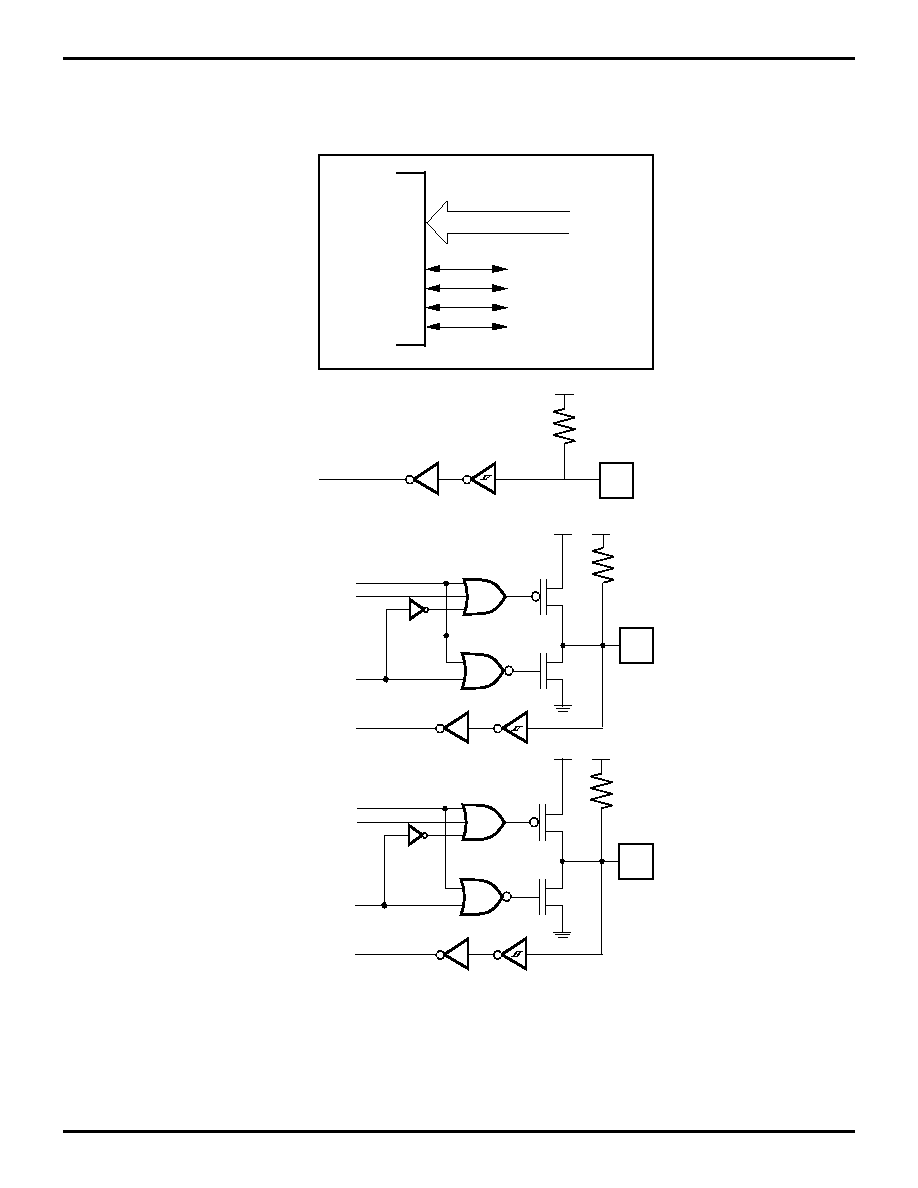
Port 0 (P07-P00). Port 0 is an 8-bit, CMOS-compatible
open-drain output (Figure 7).
Figure 7. Port 0 Configuration
Port 0
(Open-Drain
Output)
Z86KXX
8
Pad
Output
Z86K13/K14/K15/K16/K17/K18
CMOS Z8Æ 8-Bit MCU Keyboard Controllers
Zilog
10
P R E L I M I N A R Y
DS97KEY0204
Port 1 (P17-P10). Port 1 is an 8-bit CMOS compatible
open-drain output port (Figure 8).
Figure 8. Port 1 Configuration
Port 1
Open-Drain
Output
Z86KXX
Pad
Output
8
Z86K13/K14/K15/K16/K17/K18
Zilog
CMOS Z8Æ 8-Bit MCU Keyboard Controllers
DS97KEY0204
P R E L I M I N A R Y
11
1
Port 2 (P27-P20). Port 2 is an 8-bit CMOS compatible Port
with 4-bit input, 4-bit programmable I/O (Figure 9). P20-
P25 have 10.4K (
±
35%) pull-up resistors. P26-P27 have
2.4K (
±
25%) pull-up resistors.
Figure 9. Port 2 Configuration
Open-Drain
OUT
OEN
IN
Pad
2.4K
Input
(c) Ports P26-P27
Open-Drain
OUT
OEN
IN
Pad
Input
(b) Ports P24-P25
10.4 kOhm
Pad
10.4 K
Input
Z86KXX
Input
I/O
4
(a) Ports P20-P23
VCC
VCC
VCC

Z86K13/K14/K15/K16/K17/K18
CMOS Z8Æ 8-Bit MCU Keyboard Controllers
Zilog
12
P R E L I M I N A R Y
DS97KEY0204
PIN FUNCTIONS (Continued)
Port 3 (P37-P30). Port 3 is an 8-bit, CMOS-compatible
four-fixed input (P33-P30) and four-fixed output (P37-P34)
I/O port. Port 3 inputs have 10.4 Kohm pull-up resistors.
Outputs are capable of directly driving LED.
Port 3 is configured under software control to provide four
external interrupt request signals (IRQ0-IRQ3).
Figure 10. Port 3 Configuration
Port 3
Z86KXX
Output
Pad
(a) Port 3 P34-P37
(b) Port 3 P30-P33
Input
Pad
10.4 kOhms

Z86K13/K14/K15/K16/K17/K18
Zilog
CMOS Z8Æ 8-Bit MCU Keyboard Controllers
DS97KEY0204
P R E L I M I N A R Y
13
1
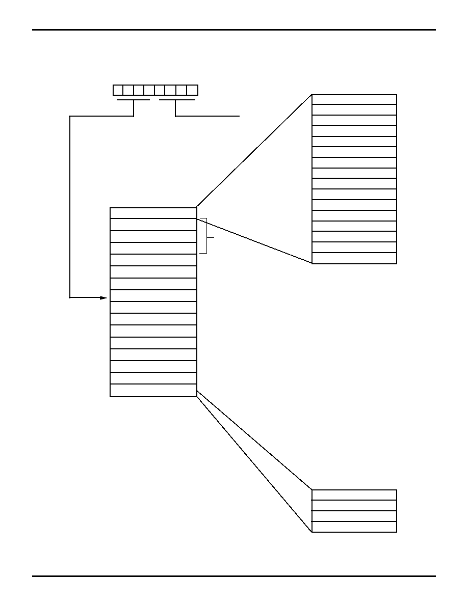
Program Memory. The 16-bit program counter addresses
4 KB of program memory space at internal locations (Fig-
ure 11).
The first 12 bytes of program memory are reserved for the
interrupt vectors. These locations have six 16-bit vectors
that correspond to the five available interrupts.
Byte 12 to byte 4095* consists of on-chip, mask pro-
grammed ROM. Addresses 4096* and greater are re-
served. (*2048 for K13/K16, 3072 for K14/K17)
Register File. The register file (Figure 13) consists of four
I/O port registers, 188 general-purpose registers (exclud-
ing P00-P03), and 11 control and status registers (R3-R0,
R191-R4, and R255-R240, respectively). The instructions
can access registers directly or indirectly through an 8-bit
address field. This allows short, 4-bit register addressing
using the Register Pointer. In the 4-bit mode, the register
file is divided into nine working-register groups, each occu-
pying 16 continuous locations. The Register Pointer ad-
dresses the starting location of the active working-register
group.
Figure 11. Program Memory Map
Figure 12. Register Pointer Register
12
11
10
9
8
7
6
5
4
3
2
1
0
On-Chip
ROM
Location of
First Byte of
Instruction
Executed
After RESET
Interrupt
Vector
(Lower Byte)
Interrupt
Vector
(Upper Byte)
Reserved
IRQ4
IRQ4
IRQ3
IRQ3
IRQ2
IRQ2
IRQ1
IRQ1
IRQ0
IRQ0
Reserved
65535
2048/3072/4096
2047/3071/4095
Reserved
D7 D6 D5 D4 D3 D2 D1 D0
R253 RP
Reserved
Working Register
Group
Default setting after RESET = 00000000
Figure 13. Register File Configuration
Stack Pointer (Bits 7-0)
R25
5
Reserved
Register Pointer
Program Control Flags
Interrupt Mask Register
Interrupt Request Register
Interrupt Priority Register
Reserved
Port 3 Mode
Port 2 Mode
T0 Prescaler
Timer/Counter0
Reserved
Reserved
Timer Mode
Reserved
Not Implemented
General-Purpose
Registers
Port 3
Port 2
Port 1
Port 0
R25
4
R253
R252
R251
R250
R249
R248
R247
R246
R245
R244
R243
R242
R241
R240
R 191
R3
R2
R1
R0
SPL
RP
FLAGS
IMR
IRQ
IPR
P3M
P2M
PREQ
T0
TMR
P3
P2
P1
P0
R4
LOCATION
IDENTIFIERS
Note:* Will not be reset with a STOP Mode Recovery.
Z86K13/K14/K15/K16/K17/K18
CMOS Z8Æ 8-Bit MCU Keyboard Controllers
Zilog
14
P R E L I M I N A R Y
DS97KEY0204
PIN FUNCTIONS (Continued)
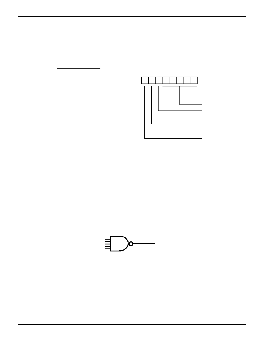
Figure 14. Register File Architecture
7
6
5
4
3
2
1
0
Working Register
Group Pointer
Reserved Register
%FF
%FO
%0F
%00
Z8 Reg. File
REGISTER POINTER
% FF
% FE
% FD
% FC
% FB
% FA
% F9
% F8
% F7
% F6
% F5
% F4
% F3
% F2
% F1
% F0
SPL
Reserved
RP
FLAGS
IMR
IRQ
IPR
Reserved
P3M
P2M
PRE0
T0
Reserved
Reserved
TMR
PORT REGISTERS
REG. GROUP (0)
REGISTER
Z8 STANDARD CONTROL REGISTERS
% (0) 03
P3
% (0) 02
P2
% (0) 01
P1
% (0) 00
P0
*
*
Reserved
Note:
*
Will not be reset with a
STOP Mode Recovery
Not
available
%BF

Z86K13/K14/K15/K16/K17/K18
Zilog
CMOS Z8Æ 8-Bit MCU Keyboard Controllers
DS97KEY0204
P R E L I M I N A R Y
15
1
Counter/Timers. There is an 8-bit programmable
counter/timer (T0) driven by its own 6-bit programmable
prescaler (Figure 15).
The 6-bit prescalers can divide the input frequency of the
clock source by any integer number from 1 to 64. The pres-
caler drives its counter, which decrements the value (1 to
256) on the prescaler overflow. When both the counter and
prescaler reach the end of count, a timer interrupt request,
IRQ4, is generated.
The counter can be programmed to start, stop, restart to
continue, or restart from the initial value. The counter can
also be programmed to stop upon reaching zero (single
pass mode) or to automatically reload the initial value and
continue counting (modulo-n continuous mode) The
counter, but not the prescaler, is read at any time without
disturbing its value or count mode.
Figure 15. Counter/Timers Block Diagram
PRE0
Initial Value
Register
T0
Initial Value
Register
T0
Current Value
Register
6-Bit
Down
Counter
8-bit
Down
Counter
˜
4
IRQ4
Write
Write
Read
Internal Data Bus
OSC

Z86K13/K14/K15/K16/K17/K18
CMOS Z8Æ 8-Bit MCU Keyboard Controllers
Zilog
16
P R E L I M I N A R Y
DS97KEY0204
PIN FUNCTIONS (Continued)
Interrupts. The Z86K15 has five different interrupts from
five different sources. These interrupts are maskable and
prioritized (Figure 16). The five sources are divided as fol-
lows: four sources are claimed by Port 3 lines P33-P30,
and the other is claimed by the counter/timer. The Interrupt
Masked Register globally or individually enables or dis-
ables the five interrupts requests.
When more than one interrupt is pending, priorities are re-
solved by a programmable priority encoder that is con-
trolled by the Interrupt Priority register. All interrupts are
vectored through locations in the program memory. When
an interrupt machine cycle is activated an interrupt request
is granted. Thus, this disables all of the subsequent inter-
rupts, saves the Program Counter and status flags, and
then branches to the program memory vector location re-
served for that interrupt. This memory location and the
next byte contain the 16-bit address of the interrupt service
routine for that particular interrupt request.
To accommodate polled interrupt systems, interrupt inputs
are masked and the interrupt request register is polled to
determine which of the interrupt request needs service.
RC Oscillator. The Z86K13/14/15 provides an internal ca-
pacitor to accommodate an RC oscillator configuration. A
1% precision resistor is necessary to achieve
±
10% accu-
rate frequency oscillation.
The Z86K15 also accepts external clock from (RCIN) with
(AGND) connected to V
CC
(Figure 17).
Figure 16. Interrupt Block Diagram
IRQ
IMR
Priority
Logic
Global
Interrupt
Enable
Vector Select
Interrupt
Request
5
IRQ0-IRQ4
5
IPR
Figure 17. RC Oscillator Configuration
RCIN
NC
1%
Precision
CLKOUT
VCC
RC Oscillator
External Clock
RCIN
AGND
VCC

Z86K13/K14/K15/K16/K17/K18
Zilog
CMOS Z8Æ 8-Bit MCU Keyboard Controllers
DS97KEY0204
P R E L I M I N A R Y
17
1
Watch-Dog Timer. The Watch-Dog Timer is activated au-
tomatically by power-on if it is enabled in the Mask Option.
The WDT is a retriggerable one-shot timer that resets the
Z8 if it reaches its terminal count. The WDT is driven by the
system clock. It must be refreshed at least once during
each time cycle by executing the WDT instruction. WDT
can be enabled by Mask Option. (Figure 18)
WDT Hot bit. Bit 7 of the Interrupt Request register (IRQ
register FAH) determines whether a hot start or cold start
occurred. A cold start is defined as reset occurring from
power-up of the Z86K15 (the default upon power-up is 0).
A hot start occurs when a WDT time-out has occurred (bit
7 is set to 1). Bit 7 of the IRQ register is read-only and is
automatically reset to 0 when read.
Watch-Dog Timer . The WDT time-out is
.
WDT During HALT (D5-R250). This bit determines wheth-
er or not the WDT is active during HALT Mode. The default
is 1, and a 1 indicates active during HALT.
294912ms
f Hz
(
)
----------------------------
Figure 18. WDT Turn-On Timing After Reset
VCC
Internal
Reset
POR
Reset
Delay
* Reset Delay = POR 147 ms
±
10% at 4 MHz.
18 Tpc
Z86K13/K14/K15/K16/K17/K18
CMOS Z8Æ 8-Bit MCU Keyboard Controllers
Zilog
18
P R E L I M I N A R Y
DS97KEY0204
PIN FUNCTIONS (Continued)
Power-On-Reset (POR). A timer circuit is triggered by the
system oscillator and is used for the Power-On Reset
(POR) timer function. The POR time allows V
CC
and the os-
cillator circuit to stabilize before instruction execution be-
gins. POR period is defined as:
The POR timer circuit is a one-shot timer triggered by one
of two conditions:
1.
Power fail to Power OK status
2.
Stop-Mode Recovery
The POR time is a nominal 147 ms
±
10%. At 4 MHz the
POR timer is bypassed after Stop-Mode Recovery.
HALT. HALT turns off the internal CPU clock, but not the
RC oscillator. The counter/timer and external interrupts
IRQ0, IRQ1, IRQ2, and IRQ3 remain active. The Z86K15
is recovered by interrupts, either externally or internally
(Figure 19).
STOP. This instruction turns off the internal clock and os-
cillator. It reduces the standby current to less than 10
µ
A.
The STOP Mode is terminated by a reset only or external
reset. This causes the processor to restart the application
program at address 000C (HEX) or the active external in-
terrupt vector. In order to enter STOP (or HALT) Mode, it
is necessary to first flush the instruction pipeline to avoid
suspending execution in mid-instruction. To do this, the
user must execute a NOP (Opcode=FFH) immediately be-
fore the appropriate sleep instruction, such as:
The Bit 6 of IRQ Registers are flags for STOP Mode Re-
covery (Figure 20).
Cold or Warm Start (D6). This bit is set upon entering
STOP Mode. A 0 (cold) indicates that the device is awak-
ened by a POR/WDT RESET. A 1 (warm) indicates that
the device is awakened by a SMR source. This bit is reset
when read.
Negative transition on any of the designated row input pins
or host data line will recover Z86KXX from STOP Mode.
POR (ms) =
589824
f
(Hz)
FF
NOP
; clear the pipeline
6F
STOP
; enter STOP Mode
or
FF
NOP
; clear the pipeline
7F
HALT
; enter HALT Mode
Figure 19. IRQ Register
D7
D6
D5
D4
D3
D2
D1
D0
R250 IRQ
IRQ0 = P32 Input
IRQ1 = P33 Input
IRQ2 = P31 Input
IRQ3 = P30 Input
IRQ4 = TO
WDT during HALT
0 OFF *
1 ON
Stop Flag
0 POR/WDT*
1 Stop Recovery
*
On RESET
WDT Hot Bit (Read Only)
0 POR*
1 WDT Timeout
Figure 20. Stop-Mode Recovery Source
To Internal
RESET
P20-P26,
P30-P33

Z86K13/K14/K15/K16/K17/K18
Zilog
CMOS Z8Æ 8-Bit MCU Keyboard Controllers
DS97KEY0204
P R E L I M I N A R Y
19
1
Z8
Æ
CONTROL REGISTER DIAGRAMS
Figure 21. Timer Mode Register
(F1
H
: Read/Write)
Counter/Timer 0 Register
Figure 22. (F4
H
: Read/Write)
Prescaler 0 Register
Figure 23. (F5
H
: Write Only)
D7
D6
D5
D4
D3
D2
D1
D0
0 = Disable T0 Count
1 = Enable T0 Count
0 = No Function
1 = Load T0
R241 TMR
Reserved (Must be 0)
D7 D6
D5
D4
D3
D2
D1
D0
T0 Initial Value
(When WRITE)
(Range: 1-256 Decimal
01-00 HEX)
T0 Current Value
(When READ)
R244 T0
D7
D6
D5
D4
D3
D2
D1
D0
Count Mode
0
0 = T Single Pass
1 = T Modulo N
0
Reserved (Must be 0)
Prescaler Modulo
(Range: 1-64 Decimal
01-00 HEX)
R245 PRE0
Port 2 Mode Register
Figure 24. (F6
H
: Write Only)
Port 2 Open Drain Mode Register
Figure 25. (F7
H
: Write Only)
Figure 26. Interrupt Priority Register
(F9
H
: Write Only)
D7
D6
D5
D4
D3
D2
D1
D0
P24-P27 I/O Definition
0 Defines Bit as OUTPUT
1 Defines Bit as INPUT
R246 P2M
Reserved
D7
D6
D5
D4
D3
D2
D1
D0
0 Port (24-27) Open-Drain
1 Port (24-27) Push-Pull
Reserved (Must be 0)
R247 P3M
D7
D6
D5
D4
D3
D2
D1
D0
Interrupt Group Priority
Reserved = 000
C > A > B = 001
A > B > C = 010
A > C > B = 011
B > C > A = 100
C > B > A = 101
B > A > C = 110
Reserved = 111
Reserved
IRQ0, IRQ2 Priority (Group B)
0 = IRQ2 > IRQ0
1 = IRQ0 > IRQ2
IRQ1, IRQ4 Priority (Group C)
0 = IRQ1 > IRQ4
1 = IRQ4 > IRQ1
Reserved (Must be 0)
R249 IPR

Z86K13/K14/K15/K16/K17/K18
CMOS Z8Æ 8-Bit MCU Keyboard Controllers
Zilog
20
P R E L I M I N A R Y
DS97KEY0204
Figure 27. Interrupt Request Register
(FA
H
: Read/Write)
Figure 28. Interrupt Mask Register
(FB
H
: Read/Write)
D7
D6
D5
D4
D3
D2
D1
D0
R250 IRQ
IRQ0 = P32 Input
IRQ1 = P33 Input
IRQ2 = P31 Input
IRQ3 = P30 Input
IRQ4 = TO
Stop Delay
0 OFF *
1 ON
Stop Flag
0 POR/WDT*
1 Stop Recovery
*
On RESET
WDT Hot Bit (Read Only)
0 POR*
1 WDT Timeout
D7
D6 D5
D4
D3
D2
D1
D0
Reserved (Must be 0)
1 Enables IRQ0-IRQ4
(D0= IRQ0)
1 Enables Interrupts
R251 IMR
Figure 29. Flag Register
(FC
H
: Read/Write)
Register Pointer
Figure 30. (FD
H
: Read/Write)
Stack Pointer
Figure 31. (FF
H
: Read/Write)
D7
D6
D5
D4
D3
D2
D1
D0
User Flag F1
User Flag F2
Half Carry Flag
Decimal Adjust Flag
Overflow Flag
Sign Flag
Zero Flag
Carry Flag
R252 Flags
D7
D6
D5
D4
D3
D2
D1
D0
Working Registers
r4
R253 RP
r5
r6
r7
Register
Pointer
D7
D6
D5
D4
D3
D2
D1
D0
Stack Pointer Lower
Byte (SP0-SP7)
R255 SPL
Z86K13/K14/K15/K16/K17/K18
Zilog
CMOS Z8Æ 8-Bit MCU Keyboard Controllers
DS97KEY0204
P R E L I M I N A R Y
21
1
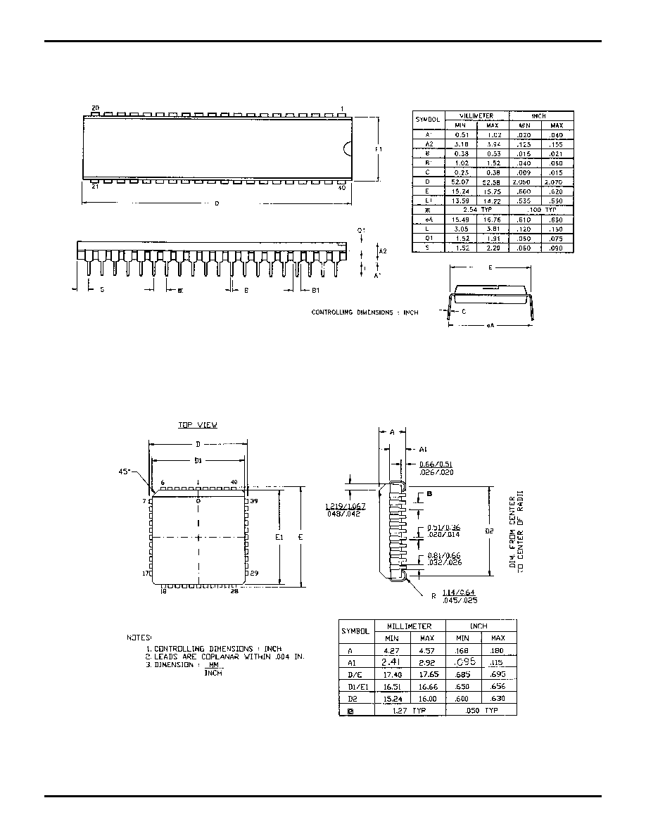
PACKAGE INFORMATION
Figure 32. 40-Pin DIP Package Diagram
Figure 33. 44-Pin PLCC Package Diagram
Z86K13/K14/K15/K16/K17/K18
CMOS Z8Æ 8-Bit MCU Keyboard Controllers
Zilog
22
P R E L I M I N A R Y
DS97KEY0204
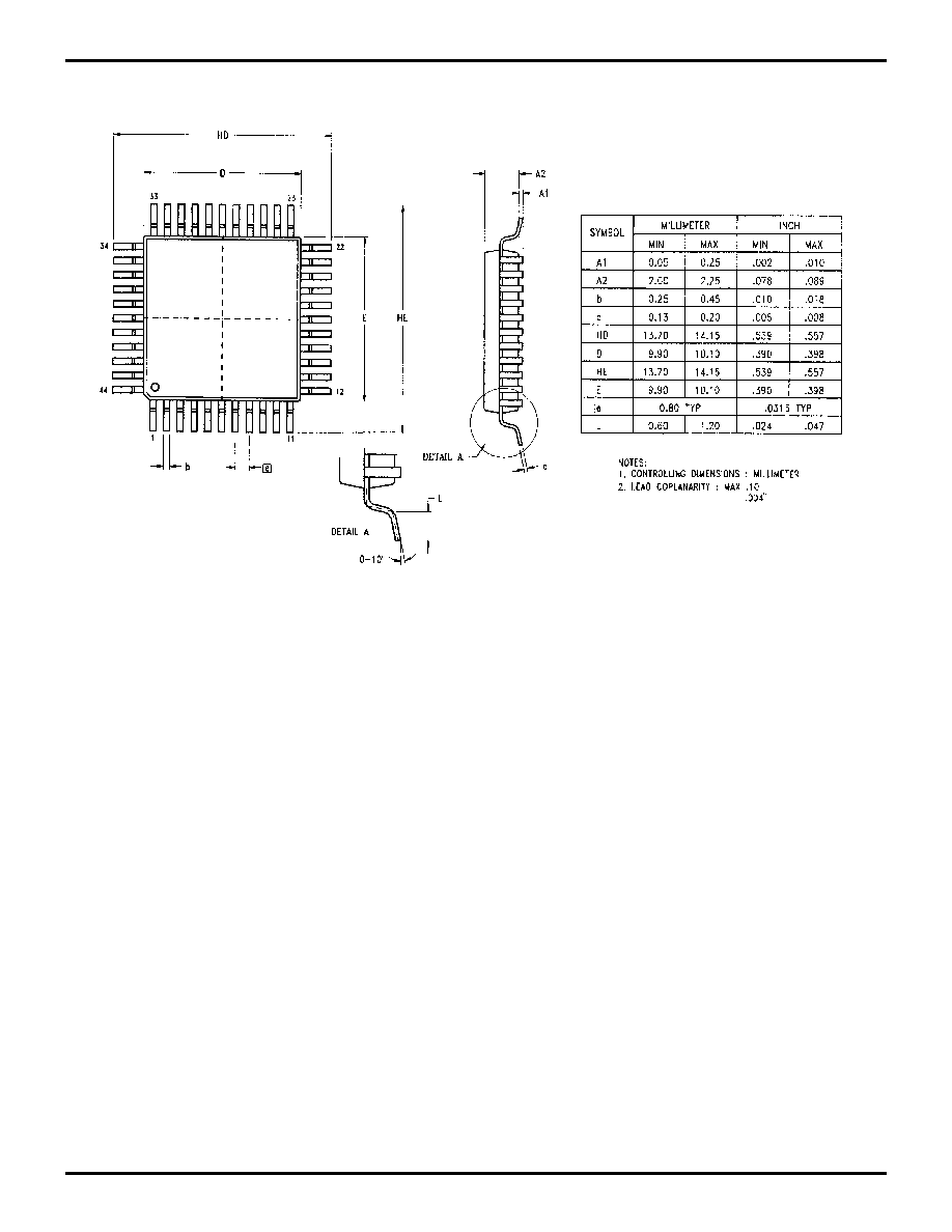
Figure 34. 44-Pin QFP Package Diagram

Z86K13/K14/K15/K16/K17/K18
Zilog
CMOS Z8Æ 8-Bit MCU Keyboard Controllers
DS97KEY0204
P R E L I M I N A R Y
23
1
ORDERING INFORMATION
For fast results, contact your local Zilog sales office for assistance in ordering the part desired.
CODES
Package
P = Plastic DIP
V = Plastic Leaded Chip Carrier
F = Quad Flat Pack
Speed
05 = 5 MHz
Environmental
C = Plastic Standard
Temperature
S = 0
∞
C to +70
∞
C
© 1997 by Zilog, Inc. All rights reserved. No part of this
document may be copied or reproduced in any form or by
any means without the prior written consent of Zilog, Inc.
The information in this document is subject to change
without notice. Devices sold by Zilog, Inc. are covered by
warranty and patent indemnification provisions appearing
in Zilog, Inc. Terms and Conditions of Sale only. Zilog, Inc.
makes no warranty, express, statutory, implied or by
description, regarding the information set forth herein or
regarding the freedom of the described devices from
intellectual property infringement. Zilog, Inc. makes no
warranty of merchantability or fitness for any purpose.
Zilog, Inc. shall not be responsible for any errors that may
appear in this document. Zilog, Inc. makes no commitment
to update or keep current the information contained in this
document.
Zilog's products are not authorized for use as critical
components in life support devices or systems unless a
specific written agreement pertaining to such intended use
is executed between the customer and Zilog prior to use.
Life support devices or systems are those which are
intended for surgical implantation into the body, or which
sustains life whose failure to perform, when properly used
in accordance with instructions for use provided in the
labeling, can be reasonably expected to result in
significant injury to the user.
Zilog, Inc. 210 East Hacienda Ave.
Campbell, CA 95008-6600
Telephone (408) 370-8000
FAX 408 370-8056
Internet: http://www.zilog.com
5 MHz
5 MHz
5 MHz
40-Pin DIP
44-Pin PLCC
44-Pin QFP
Z86KXX05PSC
Z86KXX05VSC
Z86KXX05FSC
Example:
Z 86K15 05 P S C is a Z86K15, 05 MHz, DIP, 0
∞
to +70
∞
C, Plastic Standard Flow
Environmental Flow
Temperature
Package
Speed
Product Number
Zilog Prefix

Z86K13/K14/K15/K16/K17/K18
CMOS Z8Æ 8-Bit MCU Keyboard Controllers
Zilog
24
P R E L I M I N A R Y
DS97KEY0204