
ZiLOG W
ORLDWIDE
H
EADQUARTERS
∑ 910 E. H
AMILTON
A
VENUE
∑ C
AMPBELL
, CA 95008
T
ELEPHONE
: 408.558.8500 ∑ F
AX
: 408.558.8300 ∑ I
NTERNET
:
HTTP
://
WWW
.Z
I
LOG.
COM
K
EYBOARD
C
ONTROLLER
P
RODUCT
S
PECIFICATION
PS004301-PER0100
Z86K15

Z86K15 Keyboard Controller
PS004301-PER0100
©2000 by ZiLOG, Inc. All rights reserved. Information in this publication concerning the devices, applica-
tions, or technology described is intended to suggest possible uses and may be superseded. ZiLOG, INC.
DOES NOT ASSUME LIABILITY FOR OR PROVIDE A REPRESENTATION OF ACCURACY OF
THE INFORMATION, DEVICES, OR TECHNOLOGY DESCRIBED IN THIS DOCUMENT. ZiLOG
ALSO DOES NOT ASSUME LIABILITY FOR INTELLECTUAL PROPERTY INFRINGEMENT
RELATED IN ANY MANNER TO USE OF INFORMATION, DEVICES, OR TECHNOLOGY
DESCRIBED HEREIN OR OTHERWISE. Except with the express written approval of ZiLOG, use of
information, devices, or technology as critical components of life support systems is not authorized. No
licenses are conveyed, implicitly or otherwise, by this document under any intellectual property rights.

PS004301-PER0100
Z86K15 Keyboard Controller
iii
T
ABLE
OF
C
ONTENTS
1. A
RCHITECTURAL
O
VERVIEW
. . . . . . . . . . . . . . . . . . . . . . . . . . . . . . . . . . . . . . 1
1.1 Z86K15
K
EYBOARD
C
ONTROLLER
F
EATURES
. . . . . . . . . . . . . . . . . . . . 1
1.2 F
UNCTIONAL
B
LOCK
D
IAGRAM
. . . . . . . . . . . . . . . . . . . . . . . . . . . . . . . 2
2. P
IN
D
ESCRIPTION
. . . . . . . . . . . . . . . . . . . . . . . . . . . . . . . . . . . . . . . . . . . . . 3
3. E
LECTRICAL
C
HARACTERISTICS
. . . . . . . . . . . . . . . . . . . . . . . . . . . . . . . . . . . 5
3.1 A
BSOLUTE
M
AXIMUM
R
ATINGS
. . . . . . . . . . . . . . . . . . . . . . . . . . . . . . 5
3.2 S
TANDARD
T
EST
C
ONDITIONS
. . . . . . . . . . . . . . . . . . . . . . . . . . . . . . . 5
3.3 C
APACITANCE
. . . . . . . . . . . . . . . . . . . . . . . . . . . . . . . . . . . . . . . . . . . . 6
3.4 DC
C
HARACTERISTICS
. . . . . . . . . . . . . . . . . . . . . . . . . . . . . . . . . . . . . 6
3.5 AC
E
LECTRICAL
C
HARACTERISTICS
. . . . . . . . . . . . . . . . . . . . . . . . . . . . 7
4. P
IN
F
UNCTIONS
. . . . . . . . . . . . . . . . . . . . . . . . . . . . . . . . . . . . . . . . . . . . . . 8
5. F
UNCTIONAL
D
ESCRIPTION
. . . . . . . . . . . . . . . . . . . . . . . . . . . . . . . . . . . . . 11
6. C
ONTROL
R
EGISTERS
. . . . . . . . . . . . . . . . . . . . . . . . . . . . . . . . . . . . . . . . . 20
7. P
ACKAGE
I
NFORMATION
. . . . . . . . . . . . . . . . . . . . . . . . . . . . . . . . . . . . . . . 26
8. O
RDERING
I
NFORMATION
. . . . . . . . . . . . . . . . . . . . . . . . . . . . . . . . . . . . . . 27
8.1 P
ART
N
UMBER
D
ESCRIPTION
. . . . . . . . . . . . . . . . . . . . . . . . . . . . . . . 27
9. D
OCUMENT
I
NFORMATION
. . . . . . . . . . . . . . . . . . . . . . . . . . . . . . . . . . . . . . 28
9.1 D
OCUMENT
N
UMBER
D
ESCRIPTION
. . . . . . . . . . . . . . . . . . . . . . . . . . . 28
9.2 C
HANGE
L
OG
. . . . . . . . . . . . . . . . . . . . . . . . . . . . . . . . . . . . . . . . . . . 28
C
USTOMER
F
EEDBACK
F
ORM
. . . . . . . . . . . . . . . . . . . . . . . . . . . . . . . . . . . . 29
Z86K15 K
EYBOARD
C
ONTROLLER
P
RODUCT
S
PECIFICATION
. . . . . . . . 29
C
USTOMER
I
NFORMATION
. . . . . . . . . . . . . . . . . . . . . . . . . . . . . . . . . . 29
P
RODUCT
I
NFORMATION
. . . . . . . . . . . . . . . . . . . . . . . . . . . . . . . . . . . 29
R
ETURN
I
NFORMATION
. . . . . . . . . . . . . . . . . . . . . . . . . . . . . . . . . . . . 29
P
ROBLEM
D
ESCRIPTION
OR
S
UGGESTION
. . . . . . . . . . . . . . . . . . . . . . 29

iv
Z86K15 Keyboard Controller
PS004301-PER0100

PS004301-PER0100
Z86K15 Keyboard Controller
v
L
IST
OF
F
IGURES
F
IGURE
1.
Z86K15 F
UNCTIONAL
B
LOCK
D
IAGRAM
. . . . . . . . . . . . . . . . . . . . . . . . 2
F
IGURE
2.
40-P
IN
DIP C
ONFIGURATION
. . . . . . . . . . . . . . . . . . . . . . . . . . . . . . . . 3
F
IGURE
3.
44-P
IN
PLCC C
ONFIGURATION
. . . . . . . . . . . . . . . . . . . . . . . . . . . . . . 4
F
IGURE
4.
T
EST
L
OAD
D
IAGRAM
. . . . . . . . . . . . . . . . . . . . . . . . . . . . . . . . . . . . . 5
F
IGURE
5.
A
DDITIONAL
T
IMING
. . . . . . . . . . . . . . . . . . . . . . . . . . . . . . . . . . . . . . 7
F
IGURE
6.
P
ORTS
0
AND
1 C
ONFIGURATION
. . . . . . . . . . . . . . . . . . . . . . . . . . . . . 8
F
IGURE
7.
P
ORT
2 C
ONFIGURATION
. . . . . . . . . . . . . . . . . . . . . . . . . . . . . . . . . . . 9
F
IGURE
8.
P
ORT
3 C
ONFIGURATION
. . . . . . . . . . . . . . . . . . . . . . . . . . . . . . . . . . 10
F
IGURE
9.
P
ROGRAM
M
EMORY
M
AP
. . . . . . . . . . . . . . . . . . . . . . . . . . . . . . . . . 11
F
IGURE
10. R
EGISTER
F
ILE
C
ONFIGURATION
. . . . . . . . . . . . . . . . . . . . . . . . . . . . . 12
F
IGURE
11. R
EGISTER
F
ILE
A
RCHITECTURE
. . . . . . . . . . . . . . . . . . . . . . . . . . . . . . 13
F
IGURE
12. C
OUNTER
/T
IMERS
B
LOCK
D
IAGRAM
. . . . . . . . . . . . . . . . . . . . . . . . . . 14
F
IGURE
13. I
NTERRUPT
B
LOCK
D
IAGRAM
. . . . . . . . . . . . . . . . . . . . . . . . . . . . . . . 15
F
IGURE
14. RC O
SCILLATOR
C
ONFIGURATIONS
. . . . . . . . . . . . . . . . . . . . . . . . . . 16
F
IGURE
15. WDT T
URN
-O
N
T
IMING
A
FTER
R
ESET
. . . . . . . . . . . . . . . . . . . . . . . . 17
F
IGURE
16. S
TOP
-M
ODE
R
ECOVERY
S
OURCE
. . . . . . . . . . . . . . . . . . . . . . . . . . . . 19
F
IGURE
17. 40-P
IN
DIP P
ACKAGE
D
IAGRAM
. . . . . . . . . . . . . . . . . . . . . . . . . . . . 26
F
IGURE
18. 44-P
IN
PLCC P
ACKAGE
D
IAGRAM
. . . . . . . . . . . . . . . . . . . . . . . . . . . 26

vi
Z86K15 Keyboard Controller
PS004301-PER0100

PS004301-PER0100
Z86K15 Keyboard Controller
vii
L
IST
OF
T
ABLES
T
ABLE
1.
Z86K15 K
EYBOARD
C
ONTROLLER
F
EATURES
. . . . . . . . . . . . . . . . . . . . 1
T
ABLE
2.
P
OWER
C
ONNECTIONS
. . . . . . . . . . . . . . . . . . . . . . . . . . . . . . . . . . . . 2
T
ABLE
3.
40-P
IN
DIP P
IN
I
DENTIFICATION
. . . . . . . . . . . . . . . . . . . . . . . . . . . . . . 3
T
ABLE
4.
44-P
IN
PLCC P
IN
I
DENTIFICATION
. . . . . . . . . . . . . . . . . . . . . . . . . . . . 4
T
ABLE
5.
A
BSOLUTE
M
AXIMUM
R
ATINGS
. . . . . . . . . . . . . . . . . . . . . . . . . . . . . . 5
T
ABLE
6.
C
APACITANCE
. . . . . . . . . . . . . . . . . . . . . . . . . . . . . . . . . . . . . . . . . . . 6
T
ABLE
7.
DC C
HARACTERISTICS
. . . . . . . . . . . . . . . . . . . . . . . . . . . . . . . . . . . . . 6
T
ABLE
8.
AC E
LECTRICAL
C
HARACTERISTICS
. . . . . . . . . . . . . . . . . . . . . . . . . . . . 7
T
ABLE
9.
R
EGISTER
P
OINTER
. . . . . . . . . . . . . . . . . . . . . . . . . . . . . . . . . . . . . . 13
T
ABLE
10.
I
NTERRUPT
R
EQUEST
R
EGISTER
. . . . . . . . . . . . . . . . . . . . . . . . . . . . 18
T
ABLE
11.
T
IMER
M
ODE
R
EGISTER
. . . . . . . . . . . . . . . . . . . . . . . . . . . . . . . . . . . 20
T
ABLE
12.
C
OUNTER
/T
IMER
0 R
EGISTER
. . . . . . . . . . . . . . . . . . . . . . . . . . . . . . 20
T
ABLE
13.
P
RESCALER
0 R
EGISTER
. . . . . . . . . . . . . . . . . . . . . . . . . . . . . . . . . . . 21
T
ABLE
14.
P
ORT
2 M
ODE
R
EGISTER
. . . . . . . . . . . . . . . . . . . . . . . . . . . . . . . . . . 21
T
ABLE
15.
P
ORT
2 O
PEN
D
RAIN
M
ODE
R
EGISTER
. . . . . . . . . . . . . . . . . . . . . . . 21
T
ABLE
16.
I
NTERRUPT
P
RIORITY
R
EGISTER
. . . . . . . . . . . . . . . . . . . . . . . . . . . . . 22
T
ABLE
17.
I
NTERRUPT
R
EQUEST
R
EGISTER
. . . . . . . . . . . . . . . . . . . . . . . . . . . . 23
T
ABLE
18.
I
NTERRUPT
M
ASK
R
EGISTER
. . . . . . . . . . . . . . . . . . . . . . . . . . . . . . . 23
T
ABLE
19.
F
LAG
R
EGISTER
. . . . . . . . . . . . . . . . . . . . . . . . . . . . . . . . . . . . . . . . . 24
T
ABLE
20.
R
EGISTER
P
OINTER
. . . . . . . . . . . . . . . . . . . . . . . . . . . . . . . . . . . . . . 24
T
ABLE
21.
S
TACK
P
OINTER
. . . . . . . . . . . . . . . . . . . . . . . . . . . . . . . . . . . . . . . . 25
T
ABLE
22.
O
RDERING
I
NFORMATION
. . . . . . . . . . . . . . . . . . . . . . . . . . . . . . . . . 27
T
ABLE
23.
P
ART
N
UMBER
D
ESCRIPTION
. . . . . . . . . . . . . . . . . . . . . . . . . . . . . . . 27
T
ABLE
24.
P
ACKAGE
D
ESCRIPTION
. . . . . . . . . . . . . . . . . . . . . . . . . . . . . . . . . . . 27

viii
Z86K15 Keyboard Controller
PS004301-PER0100

Z86K15 K
EYBOARD
C
ONTROLLER
F
EATURES
A
RCHITECTURAL
O
VERVIEW
PS004301-PER0100
Z86K15
1
1
ARCHITECTURAL OVERVIEW
The Z86K15 Keyboard Controller is a full-featured member of the Z8
Æ
MCU
family, offering a unique register-to-register architecture that avoids accumulator
bottlenecks. The Z86K15 is more code-efficient than RISC processors.
For keyboard applications demanding powerful I/O capabilities, the Z86K15 pro-
vides 32 pins dedicated to input and output for row, column, clock, data, and
LEDs.
An on-chip counter/timer is available to relieve the system of administering real-
time tasks.
5 different internal or external interrupt sources are maskable and prioritized to
provide a vectored address for efficient interrupt subroutine handling and multi-
tasking functions.
The Z86K15 achieves low EMI by means of several modifications in the clock
circuitry and output drivers.
1.1 Z86K15
K
EYBOARD
C
ONTROLLER
F
EATURES
Table 1 lists the features of the Z86K15 Keyboard Controller.
∑
4.5 V to 5.5 V Operating Range
∑
0∫C to +70∫C Operating Temperature Range
∑
188 Bytes of RAM
∑
Low Power Consumption: 40 mW @ 5 MHz
∑
5 Vectored, Priority Interrupts from 5 Different Sources
∑
Programmable 8-Bit Counter/Timer, with 6-Bit Programmable Prescaler
∑
Power-On Reset (POR) Timer, Hardware Watch-Dog Timer (WDT)
∑
Digital-Input CMOS Levels with Internal Pull-Up Resistors
∑
4 Direct-Connect LED Drive Ports
∑
On-Chip RC Oscillator
∑
Low System EMI Emission
∑
Z86E15 Emulation OTP
T
ABLE
1. Z86K15 K
EYBOARD
C
ONTROLLER
F
EATURES
Device
ROM
(KB)
I/O
Lines
Speed
(MHz)
Pin Count/Package
Z86K15
4
32
3≠5
40-Pin DIP, 44-Pin PLCC, Chip On Board
A
RCHITECTURAL
O
VERVIEW
F
UNCTIONAL
B
LOCK
D
IAGRAM
2
Z86K15
PS004301-PER0100
Power connections follow the conventional descriptions outlined in Table 2.
1.2 F
UNCTIONAL
B
LOCK
D
IAGRAM
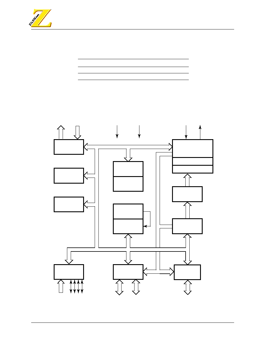
Figure 1 illustrates the functional block layout of the Z86K15 Keyboard Controller.
T
ABLE
2. P
OWER
C
ONNECTIONS
Connection
Circuit
Device
Power
V
CC
V
DD
Ground
GND
V
SS
F
IGURE
1. Z86K15 F
UNCTIONAL
B
LOCK
D
IAGRAM
Port 3
Counter/
Timer
Interrupt
Control
Port 2
I/O
(Bit Programmable)
ALU
Flags
Register
Pointer
Register File
188 x 8-Bit
Machine
Timing & Inst.
Control
WDT
POR
4 KB Program
Memory
Program
Counter
V
GND
4
4
Port 0
RC
GND
Output
Input
Input
Port 1
4
4
4
8
Open-Drain Output
with weak pull-up
Open-Drain Output
with weak pull-up
CC
IN

F
UNCTIONAL
B
LOCK
D
IAGRAM
P
IN
D
ESCRIPTION
PS004301-PER0100
Z86K15
3
2
PIN DESCRIPTION
Figure 2 illustrates the 40-pin DIP configuration for the Z86K15 Keyboard Con-
troller and Table 3 describes the pin functions.
F
IGURE
2. 40-P
IN
DIP C
ONFIGURATION
T
ABLE
3. 40-P
IN
DIP P
IN
I
DENTIFICATION
Pin #
Symbol
Function
Direction
1≠4
P30≠P33
Port 3, Pins 0,1,2,3
Input
5≠6
GND
Ground
7≠10
P27≠P24
Port 2, Pins 7,6,5,4
In/Output
11
GND
Ground
12
V
CC
Power Supply
Power
13≠20
P00≠P07
Port 0, Pins 0,1,2,3,4,5,6,7
Output
21≠28
P10≠P17
Port 1, Pins 0,1,2,3,4,5,6,7
Output
29
V
CC
Power Supply
Power
30
GND
Ground
31
GND
Ground
32
RC
IN
RC
IN
Input
33≠36
P34≠P37
Port 3, Pins 4,5,6,7
Output
37≠40
P20≠P23
Port 2, Pins 0,1,2,3
Input
P30
P31
P32
P33
GND
GND
P27
P26
P25
P24
GND
V
CC
P00
P01
P02
P03
P04
P05
P06
P07
P23
P22
P21
P20
P37
P36
P35
P34
RC
IN
GND
GND
V
CC
P17
P16
P15
P14
P13
P12
P11
P10
40
Z86K15
40-Pin DIP
1
20
21

P
IN
D
ESCRIPTION
F
UNCTIONAL
B
LOCK
D
IAGRAM
4
Z86K15
PS004301-PER0100
Figure 3 illustrates the 44-pin PLCC configuration and Table 4 describes the pin
functions.
F
IGURE
3. 44-P
IN
PLCC C
ONFIGURATION
T
ABLE
4. 44-P
IN
PLCC P
IN
I
DENTIFICATION
Pin #
Symbol
Function
Direction
1≠4
P30≠P33
Port 3, Pins 0,1,2,3
Input
5≠7
GND
Test Pins--Ground
8≠11
P27≠P24
Port 2, Pins 4,5,6,7
In/Output
12
GND
Ground
13
V
CC
Power Supply
Power
14≠21
P00≠P07
Port 0, Pins 0,1,2,3,4,5,6,7
Output
22≠28
P10≠P16
Port 1, Pins 0,1,2,3,4,5,6
Output
29
NC
Not Connected
30
P17
Port 1, Pin 7
Output
31
V
CC
Power Supply
Power
32
GND
Ground
33
AGND
Ground
34
NC
Not Connected
35
RC
IN
RC
IN
Input
36≠38
P34≠P36
Port 3, Pins 4,5,6
Output
39
NC
Not Connected
40
P37
Port 3, Pin 7
Output
41≠44
P20≠P23
Port 2, Pins 0,1,2,3
In/Output
Z86K15
44-Pin PLCC
7
17
NC
P27
P26
P25
P24
GND
V
CC
P00
P01
P02
P03
NC
P36
P35
P34
RC
IN
NC
AGND
GND
V
CC
P17
NC
P04
P05
P06
P07
P10
P11
P12
P13
P14
P15
P16
GND
GND
P33
P32
P31
P30
P23
P22
P21
P20
P37
1
28
18
40
39
29
6

A
BSOLUTE
M
AXIMUM
R
ATINGS
E
LECTRICAL
C
HARACTERISTICS
PS004301-PER0100
Z86K15
5
3
ELECTRICAL CHARACTERISTICS
3.1 A
BSOLUTE
M
AXIMUM
R
ATINGS
Table 5 provides Absolute Maximum Ratings for the Z86K15 Keyboard Controller.
Stresses greater than those listed under Absolute Maximum Ratings may cause
permanent damage to the device. This rating is a stress rating only. Functional
operation of the device at any condition above those indicated in the operational
sections of these specifications is not implied. Exposure to absolute maximum rat-
ing conditions for an extended period may affect device reliability.
Total power dissipation should not exceed 1.21 W for the package. Power dissipa-
tion is calculated as follows:
3.2 S
TANDARD
T
EST
C
ONDITIONS
The characteristics listed here apply for standard test conditions as noted. All volt-
ages are referenced to GND. Positive current flows into the referenced pin (Figure 4).
T
ABLE
5. A
BSOLUTE
M
AXIMUM
R
ATINGS
Symbol
Description
Min
Max
Units
V
CC
Supply Voltage*
≠0.3
+7.0
V
T
STG
Storage Temp
≠65
+150
∫C
I
A
Operating Ambient Temperature
0
+105
∞C
N
OTE
: *Voltage on all pins with respect to GND.
Total Power Dissipation = V
DD
x [I
DD
≠ (sum of I
OH
),
+ sum of [(V
DD
≠ V
OH
) x I
OH
]
+ sum of (V
OL
x I
OL
)
F
IGURE
4. T
EST
L
OAD
D
IAGRAM
From Output
Under Test
150 pF

E
LECTRICAL
C
HARACTERISTICS
C
APACITANCE
6
Z86K15
PS004301-PER0100
3.3 C
APACITANCE
T
A
= 25∫C; V
CC
= GND = 0 V; f = 1.0 MHz; unmeasured pins returned to GND
(see Table 6).
3.4 DC
C
HARACTERISTICS
Table 7 provides Direct Current characteristics for the Z86K15 Keyboard Controller.
T
ABLE
6. C
APACITANCE
Parameter
Max
Input Capacitance
12 pF
Output Capacitance
12 pF
I/O Capacitance
12 pF
T
ABLE
7. DC C
HARACTERISTICS
Sym Parameter
Min
Max
Unit Condition
V
CH
Clock Input High Voltage
0.7 V
CC
V
CC
+ 0.3 V
V
Driven by External Clock
Generator
V
CL
Clock Input Low Voltage
GND ≠0.3
0.2 V
CC
V
Driven by External Clock
Generator
V
IH
Input High Voltage
0.7 V
CC
V
CC
+ 0.3
V
V
IL
Input Low Voltage
GND ≠ 0.3
0.2 V
CC
V
V
OH
Output High Voltage
V
CC
≠ 0.4
V
I
OH
= ≠2.0 mA
V
OH
Output High Voltage
V
CC
≠ 0.6
V
I
OH
= ≠2.0 mA
1
V
OL
Output Low Voltage
.4
V
I
OL
= 4 mA
V
OL
Output Low Voltage
.8
V
I
OL
= 4 mA
1
I
OL
Output Low Current
10
20
mA
V
OL
= V
CC
≠2.2 V
1,2
I
OL
Output Leakage Current
≠1
1
µA
V
IN
= 0 V, 5.25 V
I
CC
V
CC
Supply Current
8
mA
@ 5.0 MHz
I
CC1
Halt Mode Current
3
mA
@ 5.0 MHz
I
CC2
Stop Mode Current
60
µA
R
P
Pull-Up Resistor
6.76
14.04
K
R
P
Pull-Up Resistor (P26≠P27)
1.8
3
K
N
OTES
:
1. V
CC
= 5.0 V ± 10% @ 0∞C to + 70∞C.
2. Ports P37≠P34. These may be used for LEDs or as general-purpose outputs requiring high sink current.\
AC E
LECTRICAL
C
HARACTERISTICS
E
LECTRICAL
C
HARACTERISTICS
PS004301-PER0100
Z86K15
7
3.5 AC
E
LECTRICAL
C
HARACTERISTICS
The ambient temperature (T
A
) range for the Z86K15 Keyboard Controller's alter-
nating current (AC) characteristics is 0∫C to 70∫C, at 5 MHz (Table 8).
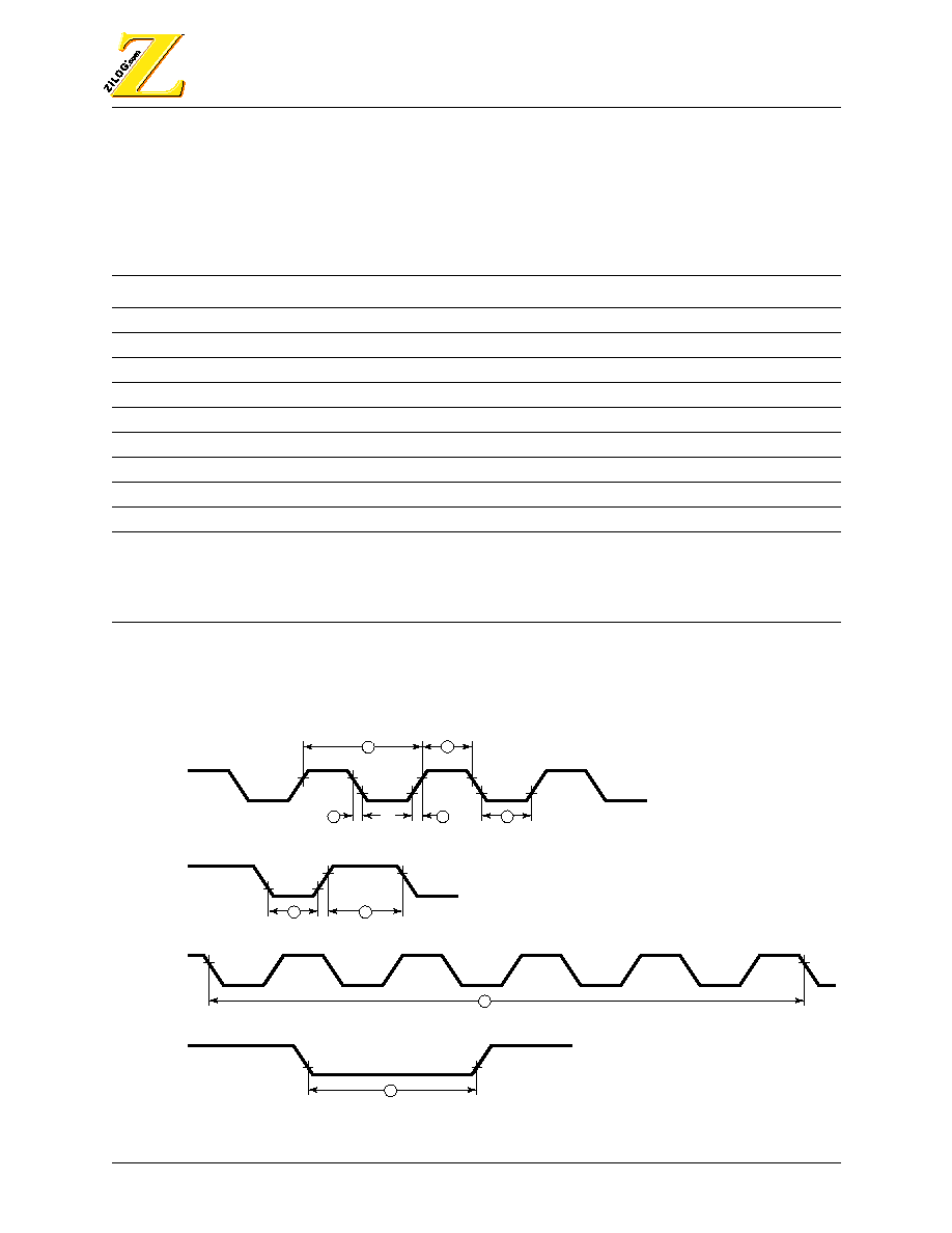
Additional timing characteristics of the Z86K15 are illustrated in Figure 5.
T
ABLE
8. AC E
LECTRICAL
C
HARACTERISTICS
No
Symbol
Parameter
V
CC
Min
Max
Units
Notes
1
TpC
Input Clock Period
5.0 V
200
333
ns
1
2
TrC, TfC
Clock Input Rise & Fall Times
5.0 V
25
ns
1
3
TwC
Input Clock Width
5.0 V
37
ns
1
4
TwIL
Interrupt Request Low Time
5.0 V
3TpC
1,2
5
TwIH
Interrupt Request Input High Time
5.0 V
3TpC
1,3
6
Tost
Oscillator Start-Up Time
5.0 V
5TpC
4
7
Twsm
Stop-Mode Recovery Width Spec
5.0 V
5TpC
ns
8
Twdt
Watch-Dog Timer Delay Time
5.0 V
53
ms
9
Tpor
Power-On Reset
5.0 V
50
200
ms
N
OTES
:
1. Timing Reference uses 0.7 V
CC
for a logic 1 and 0.2 V
CC
for a logic 0.
2. Interrupt request through Port 3 (P30).
3. Interrupt request through Port 3 (P31≠P33).
4. After Stop-Mode Recovery.
F
IGURE
5. A
DDITIONAL
T
IMING
Clock
1
3
4
2
2
3
IRQN
Clock
Stop-Mode
Recovery
7
5
Stop-Mode
Recovery
Source
6

P
IN
F
UNCTIONS
8
Z86K15
PS004301-PER0100
4
PIN FUNCTIONS
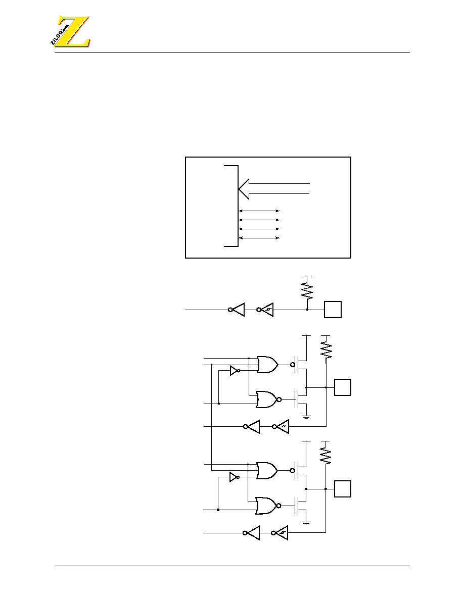
Port 0 (P07≠P00).
Port 0 is an 8-bit, CMOS-compatible, high-impedance pull-up/
low-impedance pull-down output (Figure 6).
Port 1 (P17≠P10).
Port 1 is an 8-bit, CMOS-compatible, high-impedance pull-up/
low-impedance pull-down output port (Figure 6).
F
IGURE
6. P
ORTS
0
AND
1 C
ONFIGURATION
Z86K15
PAD
Ports 0, 1
Output
H/L Output
V
CC
8
P
IN
F
UNCTIONS
PS004301-PER0100
Z86K15
9
Port 2 (P27≠P20).
Port 2 is an 8-bit CMOS-compatible Port with 4-bit input and
4-bit programmable I/O (Figure 7).
P20≠P25
feature 10.4-
K
(±35%) pull-up
resistors.
P26≠P27
feature 2.4-
K
(±25%) pull-up resistors.
N
OTE
:
Only 1 bit is used to program all 4 bits of P2
OUT
(
P24≠P27
; Open-Drain/Push-
Pull). To meet keyboard application requirements, all 4 bits are open-drain.
F
IGURE
7. P
ORT
2 C
ONFIGURATION
Out
OEN
In
2.4 K
Input
Open-Drain
Out
OEN
In
Input
(b) Ports P24≠P25
(c) Ports P26≠P27
(a) Ports P20-≠P23
10.4 K
PAD
PAD
PAD
10.4 K
Input
Z86K15
Input
I/O
4
(a) Ports P20≠P23
V
CC
V
CC
V
CC

P
IN
F
UNCTIONS
10
Z86K15
PS004301-PER0100
Port 3 (P37≠P30).
Port 3 is an 8-bit, CMOS-compatible 4-fixed input (
P33≠P30
)
and 4-fixed output (
P37≠P34
) I/O port. Port 3 inputs feature 10.4-
K
pull-up
resistors. Outputs are capable of directly driving LEDs. See Figure 8.
Port 3 is configured under software control to provide 4 external interrupt request
signals (IRQ0≠IRQ3).
F
IGURE
8. P
ORT
3 C
ONFIGURATION
Port 3
Z86K15
Output
PAD
PAD
Input
10.4 k
PAD
(a) Port 3 P34-≠P37
(b) Port 3 P30≠P33
V
CC
V
CC
10.4 K

F
UNCTIONAL
D
ESCRIPTION
PS004301-PER0100
Z86K15
11
5
FUNCTIONAL DESCRIPTION
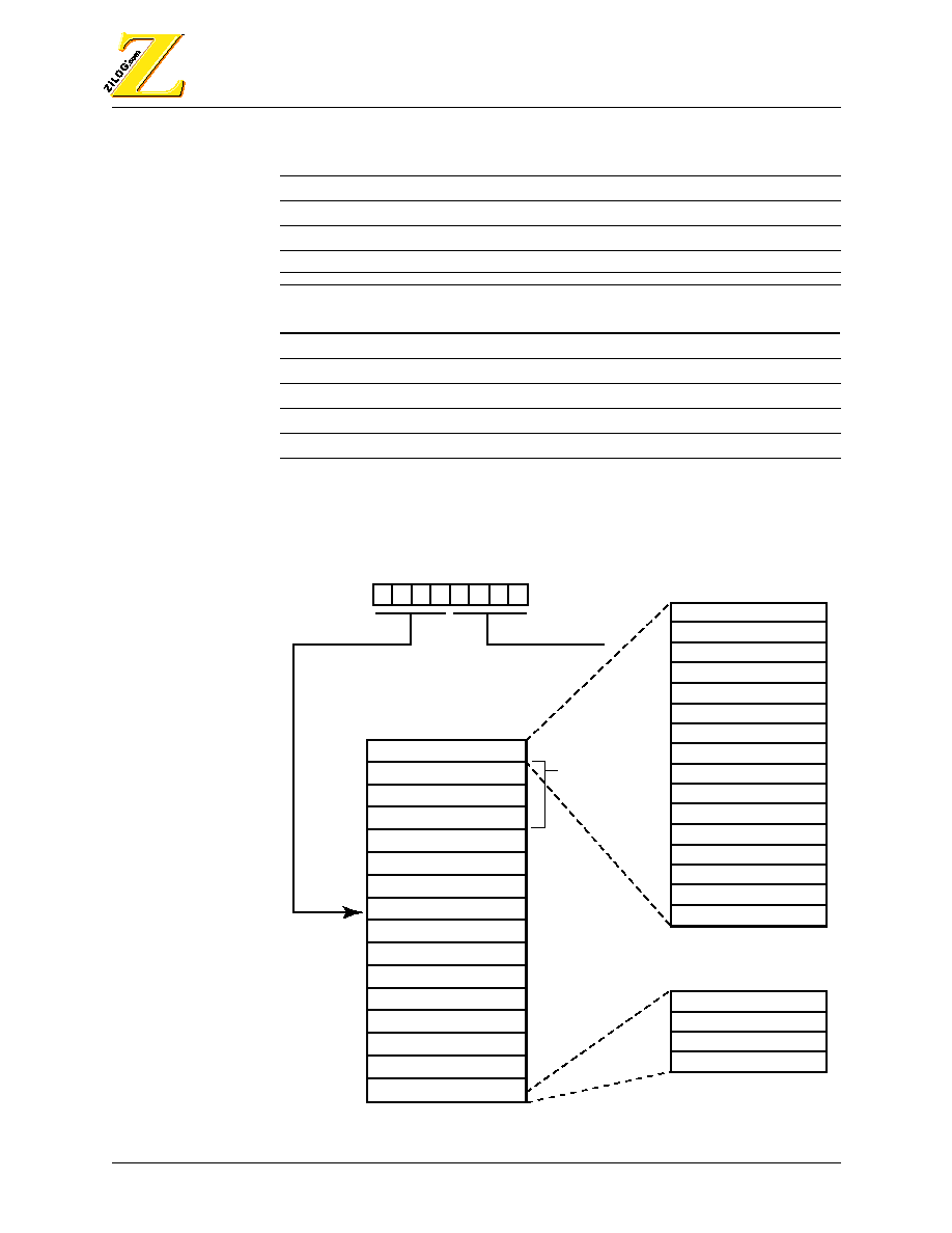
Program Memory.
The 12-bit program counter addresses 4 KB of internal pro-
gram memory space (Figure 9).
The first 12 bytes of program memory are reserved for the interrupt vectors. These
locations provide six 16-bit vectors that correspond to the 5 available interrupts.
Byte 12 to byte 4095 consist of on-chip, mask-programmed ROM. Addresses
4096 and greater are reserved.
F
IGURE
9. P
ROGRAM
M
EMORY
M
AP
12
11
10
9
8
7
6
5
4
3
2
1
0
On-Chip
ROM
Location of
First Byte of
Instruction
Executed
After RESET
Interrupt
Vector
(Lower Byte)
Interrupt
Vector
(Upper Byte)
Reserved
IRQ4
IRQ4
IRQ3
IRQ3
IRQ2
IRQ2
IRQ1
IRQ1
IRQ0
IRQ0
Reserved
65535
4096
FFFh
0Ch
4095
Reserved

F
UNCTIONAL
D
ESCRIPTION
12
Z86K15
PS004301-PER0100
Register File.
The register file (Figure 10) consists of 4 I/O port registers, 188
general-purpose registers, and 11 control and status registers (R3≠R0, R191≠R4,
and R255≠R240, respectively). The instructions can access registers directly or
indirectly through an 8-bit address field. This access allows short, 4-bit register
addressing using the Register Pointer (Table 9). In the 4-bit mode, the register file
is divided into 13 working-register groups, each occupying 16 continuous loca-
tions. The Register Pointer addresses the starting location of the active working-
register group.
For the complete Register File Assignment, refer to Figure 10.
F
IGURE
10. R
EGISTER
F
ILE
C
ONFIGURATION
Stack Pointer (Bits 7-0)
R255
Reserved
Register Pointer
Program Control Flags
Interrupt Mask Register
Interrupt Request Register
Interrupt Priority Register
Reserved
Port 2OP*
Port 2 DIR*
T0 Prescaler
Timer/Counter0
Reserved
Reserved
Timer Mode
Reserved
Not Implemented
General-Purpose
Registers
Port 3
Port 2
Port 1
Port 0
R254
R253
R252
R251
R250
R249
R248
R247
R246
R245
R244
R243
R242
R241
R240
R191
R3
R2
R1
R0
SPL
RP
FLAGS
IMR
IRQ
IPR
P2P
P2D
PREQ
T0
TMR
P3
P2
P1
P0
R4
LOCATION
IDENTIFIERS
Note: *Does not reset with a Stop-Mode Recovery.
F
UNCTIONAL
D
ESCRIPTION
PS004301-PER0100
Z86K15
13
The complete Register File Architecture is illustrated in Figure 11.
T
ABLE
9. R
EGISTER
P
OINTER
--R253 (FD
H
: R
EAD
/W
RITE
)
Bit
D7
D6
D5
D4
D3
D2
D1
D0
R/W
R/W
R/W
R/W
R/W
Reset
0
0
0
0
X
X
X
X
N
OTE
: R = Read, W = Write, X = Indeterminate.
Bit
Position
Bit
Field
R/W
Reset
Value Description
D7
r7
R/W
0
Register Pointer
D6
r6
R/W
0
Register Pointer
D5
r5
R/W
0
Register Pointer
D4
r4
R/W
0
Register Pointer
D3≠D0
Reserved
X
Reserved; must be 0
F
IGURE
11. R
EGISTER
F
ILE
A
RCHITECTURE
7
6
5
4
3
2
1
0
Working Register
Group Pointer
Reserved Register
%FF
%FO
%0F
%00
Z8 Register File
Register Pointer
% FF
% FE
% FD
% FC
% FB
% FA
% F9
% F8
% F7
% F6
% F5
% F4
% F3
% F2
% F1
% F0
SPL
Reserved
RP
FLAGS
IMR
IRQ
IPR
Reserved
P2P
P2D
PRE0
T0
Reserved
Reserved
TMR
Register Group (0)
Port Registers
Register
Z8 Standard Control Registers
% (0) 03
P3
% (0) 02
P2
% (0) 01
P1
% (0) 00
P0
*
*
Reserved
Not
available
%BF
Note: *Does not reset with a Stop-Mode Recovery.

F
UNCTIONAL
D
ESCRIPTION
14
Z86K15
PS004301-PER0100
Counter/Timers.
There is an 8-bit programmable counter/timer (T0) driven by its
own 6-bit programmable prescaler (Figure 12).
The 6-bit prescaler can divide the input frequency of the clock by any integer
number from 1 to 64. The prescaler drives its counter, which decrements the value
(1 to 256) on the prescaler overflow. When both the counter and prescaler reach
the end of count, a timer interrupt request, IRQ4, is generated.
The counter can be programmed to start, stop, restart to continue, or restart from
the initial value. The counter can also be programmed to stop upon reaching zero
(SINGLE PASS mode) or to automatically reload the initial value and continue
counting (MODULO-N CONTINUOUS mode) The counter, but not the prescaler,
can be read at any time without disturbing its value or COUNT mode.
F
IGURE
12. C
OUNTER
/T
IMERS
B
LOCK
D
IAGRAM
PRE0
Initial Value
Register
T0
Initial Value
Register
T0
Current Value
Register
IRQ4
READ
WRITE
WRITE
Internal Data Bus
˜
4
OSC
6-Bit
Down
Counter
Prescaler
8-Bit
Down
Counter

F
UNCTIONAL
D
ESCRIPTION
PS004301-PER0100
Z86K15
15
Interrupts.
The Z86K15 features 5 different interrupts from 5 different sources.
These interrupts are maskable and prioritized (Figure 13). The 5 sources are
divided as follows: 4 sources are claimed by Port 3 lines
P33≠P30
, and the other
is claimed by the counter/timer. The Interrupt Mask Register globally or individu-
ally enables or disables the 5 interrupt requests.
When more than 1 interrupt is pending, priorities are resolved by a programmable
priority encoder that is controlled by the Interrupt Priority register. All interrupts
are vectored through locations in the program memory. When an interrupt
machine cycle is activated, an interrupt request is granted, thus disabling all of the
subsequent interrupts. The program counter and status flags are saved. The inter-
rupt machine cycle then branches to the program memory vector location reserved
for the interrupt. This memory location and the next byte contain the 16-bit
address of the interrupt service routine for this particular interrupt request.
To accommodate polled interrupt systems, interrupt inputs are masked and the
interrupt request register is polled to determine which of the interrupt request
requires service.
F
IGURE
13. I
NTERRUPT
B
LOCK
D
IAGRAM
IRQ
IMR
Priority
Logic
Global
Interrupt
Enable
Vector Select
Interrupt
Request
5
IRQ0≠IRQ4
5
IPR
F
UNCTIONAL
D
ESCRIPTION
16
Z86K15
PS004301-PER0100
RC Oscillator.
The Z86K15 provides an internal capacitor to accommodate an
RC oscillator configuration. A 1% precision resistor is necessary to achieve ±10%
accurate frequency oscillation. For a nominal 4-MHz signal, use a 7.68 K
resis-
tor.
RC
IN
.
A precision resistor is connected between this pin and the power supply to
form the RC oscillator.
The Z86K15 also accepts an external clock from (RC
IN
) with AGND connected
to V
CC
(Figure 14).
F
IGURE
14. RC O
SCILLATOR
C
ONFIGURATIONS
RC
GND
CLKOUT
V
RC Oscillator
External Clock
External Clock
AGND
CC
V
CC
IN
RC
IN
1% Precision, typically
7.68K
±
1%

F
UNCTIONAL
D
ESCRIPTION
PS004301-PER0100
Z86K15
17
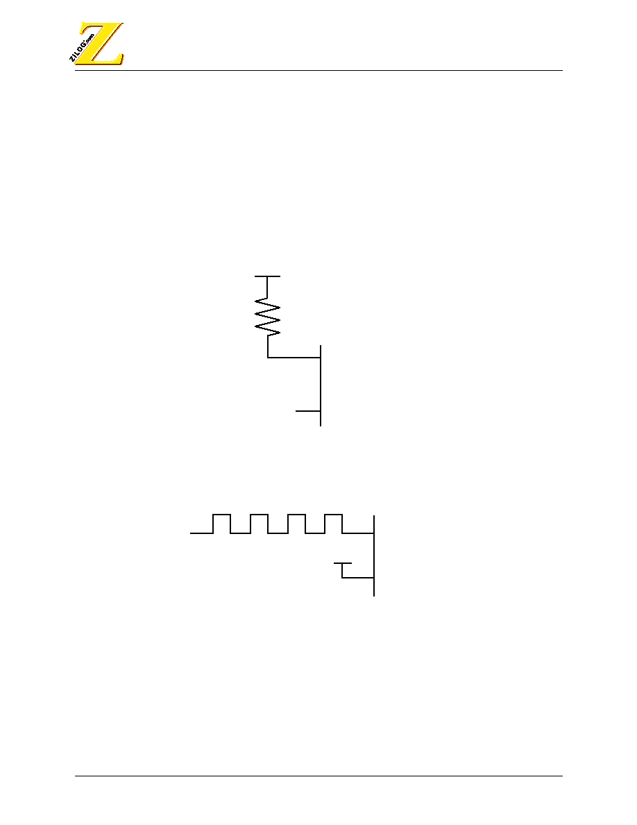
Watch-Dog Timer.
The Watch-Dog Timer (WDT) is automatically activated by
power-on when it is enabled in the Mask Option. The WDT is a retriggerable sin-
gle-shot timer that resets the Z8 if the Z8 reaches its terminal count. The WDT is
driven by the system clock. The WDT must be refreshed at least 1 time during
each WDT period by executing the WDT instruction. WDT can be enabled by
Mask Option (Figure 15).
WDT Hot Bit.
Bit 7 of the Interrupt Request register (IRQ register
FAh
) deter-
mines whether a hot start or cold start occurred. A cold start is defined as reset
occurring from power-up of the Z86K15 (the default upon power-up is 0). A hot
start occurs after a WDT time-out (bit 7 is set to 1). Bit 7 of the IRQ register is
read-only and is automatically reset to 0 when read.
Watch-Dog Timer Time-Out.
The WDT time-out is
294,912 ˜ f
.
WDT During HALT (D5≠R250).
This bit determines whether or not the WDT is
active during HALT mode. The default is 1, and a 1 indicates active during HALT.
Power-On Reset (POR).
A timer circuit is triggered by the system oscillator and
is used for the Power-On Reset (POR) timer function. The POR time allows V
CC
and the oscillator circuit to stabilize before instruction execution begins. The POR
period is defined as:
F
IGURE
15. WDT T
URN
-O
N
T
IMING
A
FTER
R
ESET
POR =
589,824
f
V
Internal
Reset
CPU Operation
POR
CC
Note: *Reset Delay = POR 50 to 200 ms.

F
UNCTIONAL
D
ESCRIPTION
18
Z86K15
PS004301-PER0100
The POR timer circuit is a single-shot timer triggered by Power Fail to Power OK
status. The POR time is a nominal 50 to 200 ms. The POR timer is bypassed dur-
ing Stop-Mode Recovery (SMR).
HALT.
HALT turns off the internal CPU clock, but not the RC oscillator. The
counter/timer and external interrupts IRQ0, IRQ1, IRQ2, and IRQ3 remain active.
The Z86K15 is recovered by interrupts, either externally or internally (Table 10).
STOP.
This instruction turns off the internal clock and oscillator, reducing the
standby current to less than 60 µA. The STOP mode is terminated by an enabled
external interrupt. This termination causes the processor to restart the application
program at address
000Ch
or the active external interrupt vector. In order to enter
STOP (or HALT) mode, it is necessary to first flush the instruction pipeline to
avoid suspending execution in mid-instruction.
To flush the pipeline, the user must execute a NOP (
Op Code = FFh
) immedi-
ately before the appropriate sleep instruction, such as:
Bit 6 of the IRQ Registers are flags for Stop-Mode Recovery (Table 10).
FF
NOP
; clear the pipeline
6F
STOP
; enter STOP mode
or
FF
NOP
; clear the pipeline
7F
HALT
; enter HALT mode
T
ABLE
10. I
NTERRUPT
R
EQUEST
R
EGISTER
--R250 IRQ (FA
H
: R
EAD
/W
RITE
)
Bit
D7
D6
D5
D4
D3
D2
D1
D0
R/W
R
R/W
R/W
R/W
R/W
R/W
R/W
R/W
Reset
0
0
0
0
0
0
0
0
N
OTE
: R = Read, W = Write, X = Indeterminate.
Bit
Position
Bit
Field
R/W
Reset
Value Description
D7
WDT
R
0
Watch-Dog Timer Hot Bit
0: POR*
1: WDT Time-out
D6
STOP
R/W
0
Stop-Mode Recovery Flag
0: POR/WDT
1: Stop Recovery
D5
WDT
R/W
0
Watch-Dog Timer During HALT Mode
0: OFF*
1: ON
D4≠D0
IRQ4≠IRQ0
R/W
0
IRQ0 = P32 Input
IRQ1 = P33 Input
IRQ2 = P31 Input
IRQ3 = P30 Input
IRQ4 = T0
N
OTE
: *Upon Reset.

F
UNCTIONAL
D
ESCRIPTION
PS004301-PER0100
Z86K15
19
Cold or Warm Start (D6).
This bit is set upon entering STOP mode. A 0 (cold)
indicates that the device is awakened by a POR/WDT RESET. A 1 (warm) indi-
cates that the device is awakened by a SMR source. This bit is reset when read.
A negative transition on the host data line or any of the designated row input pins
recover the Z86K15 from STOP mode. See Figure 16.
F
IGURE
16. S
TOP
-M
ODE
R
ECOVERY
S
OURCE
To Internal
Stop-Mode Recovery
P20≠P23, P26,
P30≠P33

C
ONTROL
R
EGISTERS
20
Z86K15
PS004301-PER0100
6
CONTROL REGISTERS
Control Register bit definitions are provided in Tables 11 through 21.
T
ABLE
11. T
IMER
M
ODE
R
EGISTER
--R241 TMR (F1
H
: R
EAD
/W
RITE
)
Bit
D7
D6
D5
D4
D3
D2
D1
D0
R/W
R/W
R/W
R/W
R/W
R/W
R/W
R/W
R/W
Reset
X
X
X
X
X
X
0
0
N
OTE
: R = Read, W = Write, X = Indeterminate.
Bit
Position
Bit
Field
R/W
Reset
Value Description
D7≠D2
Reserved
R/W
X
Reserved; must be 0
D1
T0 Count
R/W
0
Timer 0 Count
0: Disable T0 Count
1: Enable T0 Count
D0
T0
R/W
0
Timer0
0: No Function
1: Load T0
T
ABLE
12. C
OUNTER
/T
IMER
0 R
EGISTER
--R244 T0 (F4
H
: R
EAD
/W
RITE
)
Bit
D7
D6
D5
D4
D3
D2
D1
D0
R/W
R/W
R/W
R/W
R/W
R/W
R/W
R/W
R/W
Reset
X
X
X
X
X
X
X
X
N
OTE
: R = Read, W = Write, X = Indeterminate.
Bit
Position
Bit
Field
R/W
Reset
Value Description
D7≠D0
T0 Initial
Value
R/W
X
Timer0 Initial Value when WRITE;
range = 1≠256 decimal, 01≠100 hex
T0 Current
Value
R/W
X
Timer0 Current Value when READ

C
ONTROL
R
EGISTERS
PS004301-PER0100
Z86K15
21
T
ABLE
13. P
RESCALER
0 R
EGISTER
--R245 PRE0 (F5
H
: W
RITE
O
NLY
)
Bit
D7
D6
D5
D4
D3
D2
D1
D0
R/W
W
W
W
W
W
W
W
W
Reset
X
X
X
X
X
X
X
X
N
OTE
: W = Write, X = Indeterminate.
Bit
Position
Bit
Field
R/W
Reset
Value Description
D7≠D2
Prescaler
W
X
Prescaler Modulo; range = 1≠64
decimal, 01≠40 hex
D1
Reserved
W
X
Reserved; must be 0
D0
Count
W
X
COUNT Mode
0: T0 Single Pass
1: T0 Modulo N
T
ABLE
14. P
ORT
2 M
ODE
R
EGISTER
--R246 P2D (F6
H
: W
RITE
O
NLY
)
Bit
D7
D6
D5
D4
D3
D2
D1
D0
R/W
W
W
W
W
W
W
W
W
Reset
1
1
1
1
0
0
0
0
N
OTE
: W = Write.
Bit
Position
Bit
Field
R/W
Reset
Value Description
D7≠D4
P24≠P27
W
1
P24≠P27 I/O Definition
0: Defines bit as Output
1: Defines bit as Input
D3≠D0
Reserved
W
0
Reserved; must be 0
T
ABLE
15. P
ORT
2 O
PEN
D
RAIN
M
ODE
R
EGISTER
--R247 P2P (F7
H
: W
RITE
O
NLY
)
Bit
D7
D6
D5
D4
D3
D2
D1
D0
R/W
W
W
W
W
W
W
W
W
Reset
0
0
0
0
0
0
0
X
N
OTE
: W = Write, X = Indeterminate.
Bit
Position
Bit
Field
R/W
Reset
Value Description
D7≠D1
Reserved
W
0
Reserved; must be 0
D0
P24≠P27
W
0: P24≠P27 Open-Drain*
1: P24≠P27 Push-Pull
N
OTE
: Must be open-drain to satisfy PS/2 operation.

C
ONTROL
R
EGISTERS
22
Z86K15
PS004301-PER0100
T
ABLE
16. I
NTERRUPT
P
RIORITY
R
EGISTER
--R249 IPR (F9
H
: W
RITE
O
NLY
)
Bit
D7
D6
D5
D4
D3
D2
D1
D0
R/W
W
W
W
W
W
W
W
W
Reset
X
X
X
X
X
X
X
X
N
OTE
: W = Write, X = Indeterminate.
Bit
Position
Bit
Field
R/W
Reset
Value Description
D7≠D6
Reserved
W
X
Reserved; must be 0
D5
Reserved
W
X
Reserved
D4≠D3,
D0
Interrupt
W
X
Interrupt Group Priority
Reserved = 000
C > A > B = 001
A > B > C = 010
A > C > B = 011
B > C > A = 100
C > B > A = 101
B > A > C = 110
Reserved = 111
D2
IRQ0, IRQ4
W
X
IRQ0, IRQ4 Priority (Group C)
0: IRQ1 > IRQ4
1: IRQ4 > IRQ1
D1
IRQ0, IRQ2
W
X
IRQ0, IRQ2 Priority (Group B)
0: IRQ2 > IRQ0
1: IRQ0 > IRQ2

C
ONTROL
R
EGISTERS
PS004301-PER0100
Z86K15
23
T
ABLE
17. I
NTERRUPT
R
EQUEST
R
EGISTER
--R250 IRQ (FA
H
: R
EAD
/W
RITE
)
Bit
D7
D6
D5
D4
D3
D2
D1
D0
R/W
R
R/W
R/W
R/W
R/W
R/W
R/W
R/W
Reset
0
0
0
0
0
0
0
0
N
OTE
: R = Read, W = Write.
Bit
Position
Bit
Field
R/W
Reset
Value Description
D7
WDT
R
0
Watch-Dog Timer Hot Bit
0: POR*
1: WDT Time-out
D6
STOP
R/W
0
Stop Flag
0: POR/WDT
1: Stop-Mode Recovery
D5
STOP
R/W
0
Stop Delay
0: OFF*
1: ON
D4≠D0
IRQ4≠IRQ0
R/W
0
IRQ0 = P32 Input
IRQ1 = P33 Input
IRQ2 = P31 Input
IRQ3 = P30 Input
IRQ4 = T0
N
OTE
: Upon Reset.
T
ABLE
18. I
NTERRUPT
M
ASK
R
EGISTER
--R251 IMR (FB
H
: R
EAD
/W
RITE
)
Bit
D7
D6
D5
D4
D3
D2
D1
D0
R/W
R/W
R/W
R/W
R/W
R/W
R/W
R/W
R/W
Reset
0
X
X
0
0
0
0
0
N
OTE
: R = Read, W = Write, X = Indeterminate.
Bit
Position
Bit
Field
R/W
Reset
Value Description
D7
Interrupt
R/W
0
1: Enables Interrupts
D6≠D5
Reserved
R/W
X
Reserved; must be 0
D4≠D0
IRQ4≠IRQ0
R/W
0
1: Enables IRQ0≠IRQ4; D0 = IRQ0

C
ONTROL
R
EGISTERS
24
Z86K15
PS004301-PER0100
T
ABLE
19. F
LAG
R
EGISTER
--R252 (FC
H
: R
EAD
/W
RITE
)
Bit
D7
D6
D5
D4
D3
D2
D1
D0
R/W
R/W
R/W
R/W
R/W
R/W
R/W
R/W
R/W
Reset
0
0
0
0
0
0
0
0
N
OTE
: R = Read, W = Write.
Bit
Position
Bit
Field
R/W
Reset
Value Description
D7
R/W
0
Carry Flag
D6
R/W
0
Zero Flag
D5
R/W
0
Sign Flag
D4
R/W
0
Overflow Flag
D3
R/W
0
Decimal Adjust Flag
D2
R/W
0
Half Carry Flag
D1
R/W
0
User Flag F2
D0
R/W
0
User Flag F1
T
ABLE
20. R
EGISTER
P
OINTER
--R253 (FD
H
: R
EAD
/W
RITE
)
Bit
D7
D6
D5
D4
D3
D2
D1
D0
R/W
R/W
R/W
R/W
R/W
R/W
R/W
R/W
R/W
Reset
0
0
0
0
X
X
X
X
N
OTE
: R = Read, W = Write, X = Indeterminate.
Bit
Position
Bit
Field
R/W
Reset
Value Description
D7
r7
R/W
0
Register Pointer
D6
r6
R/W
0
Register Pointer
D5
r5
R/W
0
Register Pointer
D4
r4
R/W
0
Register Pointer
D3≠D0
Reserved
R/W
X
Reserved; must be 0

C
ONTROL
R
EGISTERS
PS004301-PER0100
Z86K15
25
T
ABLE
21. S
TACK
P
OINTER
--R255 (FF
H
: R
EAD
/W
RITE
)
Bit
D7
D6
D5
D4
D3
D2
D1
D0
R/W
R/W
R/W
R/W
R/W
R/W
R/W
R/W
R/W
Reset
X
X
X
X
X
X
X
X
N
OTE
: R = Read, W = Write, X = Indeterminate.
Bit
Position
Bit
Field
R/W
Reset
Value Description
D7≠D0
SP0≠SP7
R/W
X
Stack Pointer

P
ACKAGE
I
NFORMATION
26
Z86K15
PS004301-PER0100
7
PACKAGE INFORMATION
Figures 17 and 18 illustrate the 40-pin DIP and the 44-pin PLCC packages,
respectively.
F
IGURE
17. 40-P
IN
DIP P
ACKAGE
D
IAGRAM
F
IGURE
18. 44-P
IN
PLCC P
ACKAGE
D
IAGRAM

P
ART
N
UMBER
D
ESCRIPTION
O
RDERING
I
NFORMATION
PS004301-PER0100
Z86K15
27
8
ORDERING INFORMATION
Ordering Information for the Z86K15 Keyboard Controller is provided in Table 22.
8.1 P
ART
N
UMBER
D
ESCRIPTION
ZiLOG part numbers consist of a number of components, as indicated in Tables
23 and 24:
E
XAMPLE
:
Part number Z86K1505PSC is a Z86K15 MCU, a 5-MHz dual-inline package
with 0∫C to +70∫C temperature range and Plastic Standard environmental flow.
For fast results, contact your local ZiLOG sales office for assistance in ordering
the part required.
T
ABLE
22. O
RDERING
I
NFORMATION
Part
PSI
Description
Z86K15
Z86K1505PSC
40-Pin DIP, 5 MHz, Standard Temperature
Z86K1505VSC
44-Pin PLCC, 5 MHz, Standard Temperature
T
ABLE
23. P
ART
N
UMBER
D
ESCRIPTION
Z
ZiLOG prefix
86K15
Product Number
05
Speed
P
Package
S
Temperature
C
Environmental Flow
T
ABLE
24. P
ACKAGE
D
ESCRIPTION
Preferred Package
P = Plastic DIP
V = Plastic Chip Carrier
Preferred Temperature
S = 0∞C to +70∞C
Speed
5 = 5 MHz
Environmental
C = Plastic Standard

D
OCUMENT
I
NFORMATION
D
OCUMENT
N
UMBER
D
ESCRIPTION
28
Z86K15
PS004301-PER0100
9
DOCUMENT INFORMATION
9.1 D
OCUMENT
N
UMBER
D
ESCRIPTION
The Document Control Number that appears in the footer of each page of this
document contains unique identifying attributes, as indicated in the following
table:
9.2 C
HANGE
L
OG
PS
Product Specification
0043
Unique Document Number
01
Revision Number
PER
Business Channel
0100
Month and Year Published
Rev
Date
Purpose
By
01
01/00
Original issue
J. Irwin

Z86K15 K
EYBOARD
C
ONTROLLER
P
RODUCT
S
PECIFICATION
C
USTOMER
F
EEDBACK
F
ORM
PS004301-PER0100
Z86K15
29
CUSTOMER FEEDBACK FORM
Z86K15 K
EYBOARD
C
ONTROLLER
P
RODUCT
S
PECIFICATION
If you experience any problems while operating this product, or if you note any
inaccuracies while reading this Product Specification, please copy and complete
this form, then mail or fax it to ZiLOG (see Return Information, below). We also
welcome your suggestions!
C
USTOMER
I
NFORMATION
P
RODUCT
I
NFORMATION
R
ETURN
I
NFORMATION
ZiLOG
System Test/Customer Support
910 E. Hamilton Avenue, Suite 110, MS 4≠3
Campbell, CA 95008
Fax: (408) 558-8536
Email: tools@zilog.com
P
ROBLEM
D
ESCRIPTION
OR
S
UGGESTION
Provide a complete description of the problem or your suggestion. If you are
reporting a specific problem, include all steps leading up to the occurrence of the
problem. Attach additional pages as necessary.
________________________________________________________________________
________________________________________________________________________
________________________________________________________________________
________________________________________________________________________
________________________________________________________________________
________________________________________________________________________
Name
Country
Company
Phone
Address
Fax
City/State/Zip
E-Mail
Serial # or Board Fab #/Rev. #
Software Version
Document Number
Host Computer Description/Type

C
USTOMER
F
EEDBACK
F
ORM
P
ROBLEM
D
ESCRIPTION
OR
S
UGGESTION
30
Z86K15
PS004301-PER0100

PS004301-PER0100
Z86K15 Keyboard Controller
31
I
NDEX
N
UMERICS
40-Pin DIP Configuration
. . . . . . . . . . . . . . . 3
40-Pin DIP Pin Identification
. . . . . . . . . . . . 3
44-Pin PLCC Configuration
. . . . . . . . . . . . . 4
44-Pin PLCC Pin Identification
. . . . . . . . . . 4
4-bit mode
. . . . . . . . . . . . . . . . . . . . . . . . . . 12
A
Absolute Maximum Ratings
. . . . . . . . . . . . . 5
AC Electrical Characteristics
. . . . . . . . . . . . 7
alternating current
. . . . . . . . . . . . . . . . . . . . . 7
ambient temperature range
. . . . . . . . . . . . . . 7
Architectural Overview
. . . . . . . . . . . . . . . . . 1
B
bit definitions
. . . . . . . . . . . . . . . . . . . . . . . 20
C
Capacitance
. . . . . . . . . . . . . . . . . . . . . . . . . . 6
Change Log
. . . . . . . . . . . . . . . . . . . . . . . . . 28
clock circuitry
. . . . . . . . . . . . . . . . . . . . . . . . 1
cold start
. . . . . . . . . . . . . . . . . . . . . . . . . . . 19
Control Registers
. . . . . . . . . . . . . . . . . . . . . 20
Counter/Timer
. . . . . . . . . . . . . . . . . 14-15
,
18
Counter/Timer 0 Register
. . . . . . . . . . . . . . 20
Customer Feedback Form
. . . . . . . . . . . . . . 29
Customer Information
. . . . . . . . . . . . . . . . . 29
D
DC Characteristics
. . . . . . . . . . . . . . . . . . . . 6
Direct Current
. . . . . . . . . . . . . . . . . . . . . . . . 6
Document Information
. . . . . . . . . . . . . . . . 28
Document Number Description
. . . . . . . . . 28
E
Electrical Characteristics
. . . . . . . . . . . . . . . . 5
external interrupt request
. . . . . . . . . . . . . . . 10
external interrupts
. . . . . . . . . . . . . . . . . . . . 18
F
Functional Block Diagram
. . . . . . . . . . . . . . 2
Functional Description
. . . . . . . . . . . . . . . . 11
G
GND
. . . . . . . . . . . . . . . . . . . . . . . . . . . . . . . 2
H
host data line
. . . . . . . . . . . . . . . . . . . . . . . . 19
I
input frequency
. . . . . . . . . . . . . . . . . . . . . . 14
internal CPU clock
. . . . . . . . . . . . . . . . . . . 18
Interrupt Mask Register
. . . . . . . . . . . . 15
,
23
Interrupt Priority Register
. . . . . . . . . . . 15, 22
Interrupt Request
. . . . . . . . . . . . . 7
,
14-15, 17
Register
. . . . . . . . . . . . . . . . . . . . . . . 18
,
23
interrupt sources
. . . . . . . . . . . . . . . . . . . . . . 1
interrupt subroutine handling
. . . . . . . . . . . . 1
interrupt vector
. . . . . . . . . . . . . . . . . . . 11
,
18
Interrupts
. . . . . . . . . . . . . . . . . . . 1
,
11, 15
,
23
IRQ0
. . . . . . . . . . . . . . . . . . . . . 10
,
18
,
22
,
23
IRQ1
. . . . . . . . . . . . . . . . . . . . . . . . 18
,
22
,
23
IRQ2
. . . . . . . . . . . . . . . . . . . . . . . . 18
,
22
,
23
IRQ3
. . . . . . . . . . . . . . . . . . . . . . . . 10
,
18
,
23
IRQ4
. . . . . . . . . . . . . . . . . . . . . 14
,
18
,
22
,
23
L
Low Power Consumption
. . . . . . . . . . . . . . . 1
M
modulo-n continuous mode
. . . . . . . . . . . . 14
multitasking
. . . . . . . . . . . . . . . . . . . . . . . . . 1
N
NOP
. . . . . . . . . . . . . . . . . . . . . . . . . . . . . . 18
O
on-chip counter/timer
. . . . . . . . . . . . . . . . . . 1
Op Code
. . . . . . . . . . . . . . . . . . . . . . . . . . . 18
Open-Drain
. . . . . . . . . . . . . . . . . . . . . . . 9
,
21
Operating Range
. . . . . . . . . . . . . . . . . . . . . . 1
Operating Temperature
. . . . . . . . . . . . . . . . . 1
Ordering Information
. . . . . . . . . . . . . . . . . 27
output drivers
. . . . . . . . . . . . . . . . . . . . . . . . 1
P
P2OUT
. . . . . . . . . . . . . . . . . . . . . . . . . . . . . 9

32
Z86K15 Keyboard Controller
PS004301-PER0100
Package Information
. . . . . . . . . . . . . . . . . . 26
Part Number Description
. . . . . . . . . . . . . . . 27
Pin Description
. . . . . . . . . . . . . . . . . . . . . . . 3
Pin Functions
. . . . . . . . . . . . . . . . . . . . . . . . . 8
POR
. . . . . . . . . . . . . . . . . . . . . . .1
,
17
,
19
,
23
timer circuit
. . . . . . . . . . . . . . . . . . . . . . . 18
Port 0
. . . . . . . . . . . . . . . . . . . . . . . . . . . 3
,
4
,
8
Port 1
. . . . . . . . . . . . . . . . . . . . . . . . . . . 3
,
4
,
8
Port 2
. . . . . . . . . . . . . . . . . . . . . . . . . . . 3
,
4
,
9
Port 2 Mode Register
. . . . . . . . . . . . . . . . . 21
Port 2 Open Drain Mode Register
. . . . . . . . 21
Port 3
. . . . . . . . . . . . . . . . . . . . . 3
-
4
,
7
,
10
,
15
Power connections
. . . . . . . . . . . . . . . . . . . . 2
Power Fail
. . . . . . . . . . . . . . . . . . . . . . . . . . 18
Power OK
. . . . . . . . . . . . . . . . . . . . . . . . . . 18
Power-On Reset
. . . . . . . . . . . . . . . . . 1
,
7
,
17
Prescaler
. . . . . . . . . . . . . . . . . . . . . . . . . 1, 14
Prescaler 0 Register
. . . . . . . . . . . . . . . . . . . 21
prescaler overflow
. . . . . . . . . . . . . . . . . . . . 14
Problem Description or Suggestion
. . . . . . 29
Product Information
. . . . . . . . . . . . . . . . . . 29
programmable priority encoder
. . . . . . . . . . 15
Pull-Up Resistor
. . . . . . . . . . . . . . . . . . . . 1
,
6
Push-Pull
. . . . . . . . . . . . . . . . . . . . . . . . . 9
,
21
R
RC Oscillator
. . . . . . . . . . . . . . . . . . . 1
,
16, 18
real-time tasks
. . . . . . . . . . . . . . . . . . . . . . . . 1
register addressing
. . . . . . . . . . . . . . . . . . . . 12
Register File Assignment
. . . . . . . . . . . . . . 12
Register Pointer
. . . . . . . . . . . . . . . . 12
-
13
,
24
Return Information
. . . . . . . . . . . . . . . . . . . 29
S
SINGLE PASS mode
. . . . . . . . . . . . . . . . . 14
sleep instruction
. . . . . . . . . . . . . . . . . . . . . 18
SMR
. . . . . . . . . . . . . . . . . . . . . . . . . . . . . . 18
source
. . . . . . . . . . . . . . . . . . . . . . . . . . . 19
Standard Test Conditions
. . . . . . . . . . . . . . . 5
standby current
. . . . . . . . . . . . . . . . . . . . . . 18
Stop Delay
. . . . . . . . . . . . . . . . . . . . . . . . . . 23
Stop Flag
. . . . . . . . . . . . . . . . . . . . . . . . . . . 23
Stop-Mode Recovery
. . . . . . . . . . . . . . . 7
,
18
T
Total power dissipation
. . . . . . . . . . . . . . . . . 5
V
V
CC
. . . . . . . . . . . . . . . . . . . . . . . . . . . . . . . . 2
W
warm start
. . . . . . . . . . . . . . . . . . . . . . . . . . 19
Watch-Dog Timer
. . . . . . . . . . 1
,
7
,
17
-
18
,
23
Time-Out
. . . . . . . . . . . . . . . . . . . . . . . . 17
WDT
. . . . . . . . . . . . . . . . . . . . . . . . . . . . 1
,
17
During HALT
. . . . . . . . . . . . . . . . . . . . . 17
Hot Bit
. . . . . . . . . . . . . . . . . . . . . . . . . . 17
Time-out
. . . . . . . . . . . . . . . . . . . 17-18
,
23
working-register groups
. . . . . . . . . . . . . . . 12
Z
Z86E15 Emulation OTP
. . . . . . . . . . . . . . . . 1
Z86K15 Keyboard Controller Features
. . . . 1