DS96LV00800
P R E L I M I N A R Y
1
1
P
RELIMINARY
P
RODUCT
S
PECIFICATION
Z86L88/81/86/87/89/73
1
IR/L
OW
-V
OLTAGE
M
ICROCONTROLLER
FEATURES
s
Low Power Consumption - 40 mW (Typical)
s
Three Standby Modes
�
STOP
�
HALT
�
Low Voltage
s
Special Architecture to Automate Both Generation and
Reception of Complex Pulses or Signals:
�
One Programmable 8-Bit Counter/Timer with Two
Capture Registers
�
One Programmable 16-Bit Counter/Timer with
One 16-Bit Capture Register
�
Programmable Input Glitch Filter for Pulse
Reception
s
Five Priority Interrupts
�
Three External
�
Two Assigned to Counter/Timers
s
Low Voltage Detection and Standby Mode
s
Programmable Watch-Dog/Power-On Reset Circuits
s
Two Independent Comparators with Programmable
Interrupt Polarity
s
On-Chip Oscillator that Accepts a Crystal, Ceramic
Resonator, LC, RC (Mask Option), or External Clock
Drive
s
Mask Selectable 200 kOhms Pull-Ups on Ports 0, 2, 3
�
All Eight Port 2 Bits at One Time or Not
�
Pull-Ups Automatically Disabled Upon Selecting
Individual Pins as Outputs.
s
Maskable Mouse/Trackball Interface on P00 Through
P03.
s
32 kHz Oscillator Mask Option
GENERAL DESCRIPTION
The Z86LXX family of IR (Infrared) CCP
TM
(Consumer Con-
troller Processor) Controllers are ROM/ROMless-based
members of the Z8
�
single-chip microcontroller family with
256 bytes of internal RAM. The differentiating factor be-
tween these devices is the availability of ROM, and pack-
age options. For the 40 and 44-pin devices the use of ex-
ternal memory enables these Z8 microcontrollers to be
used where code flexibility is required. Zilog's CMOS mi-
crocontrollers offers fast executing, efficient use of memo-
ry, sophisticated interrupts, input/output bit manipulation
capabilities, automated pulse generation/reception, and in-
ternal key-scan pull-up resistors. The Z86LXX product line
offers easy hardware/software system expansion cost-ef-
fective and low power consumption.
The Z86LXX architecture is based on Zilog's 8-bit micro-
controller core with an Expanded Register File to allow ac-
cess to register mapped peripherals, I/O circuits, and pow-
erful counter/timer circuitry. The CCP offers a flexible I/O
scheme, an efficient register and address space structure,
and a number of ancillary features that are useful in many
Device
ROM
(KB)
RAM*
(Bytes)
I/O
Lines
Voltage
Range
Z86L88
16
237
23
2.0V to 3.9V
Z86L81
24
237
23
2.0V to 3.9V
Z86L86
32
237
23
2.0V to 3.9V
Z86L87
16
236
31
2.0V to 3.9V
Z86L89
24
236
31
2.0V to 3.9V
Z86L73
32
236
31
2.0V to 3.9V
Note:
*General-Purpose
Z86L88/81/86/87/89/73
IR/Low-Voltage Microcontroller
2
P R E L I M I N A R Y
DS96LV00800
GENERAL DESCRIPTION
(Continued)
consumer, automotive, computer peripheral, and battery
operated hand-held applications.
There are four basic address spaces available to support
a wide range of configurations: Program Memory, Regis-
ter File, Expanded Register File, and External Memory.
The register file is composed of 256 bytes of RAM. It in-
cludes four I/O port registers, 16 control and status regis-
ters and the rest are General Purpose registers. The Ex-
panded Register File consists of two additional register
groups (F and D). External Memory is not available on 28-
pin versions.
To unburden the program from coping with such real-time
problems as generating complex waveforms or receiving
and demodulating complex waveform/pulses, the Z86LXX
family offers a new intelligent counter/timer architecture
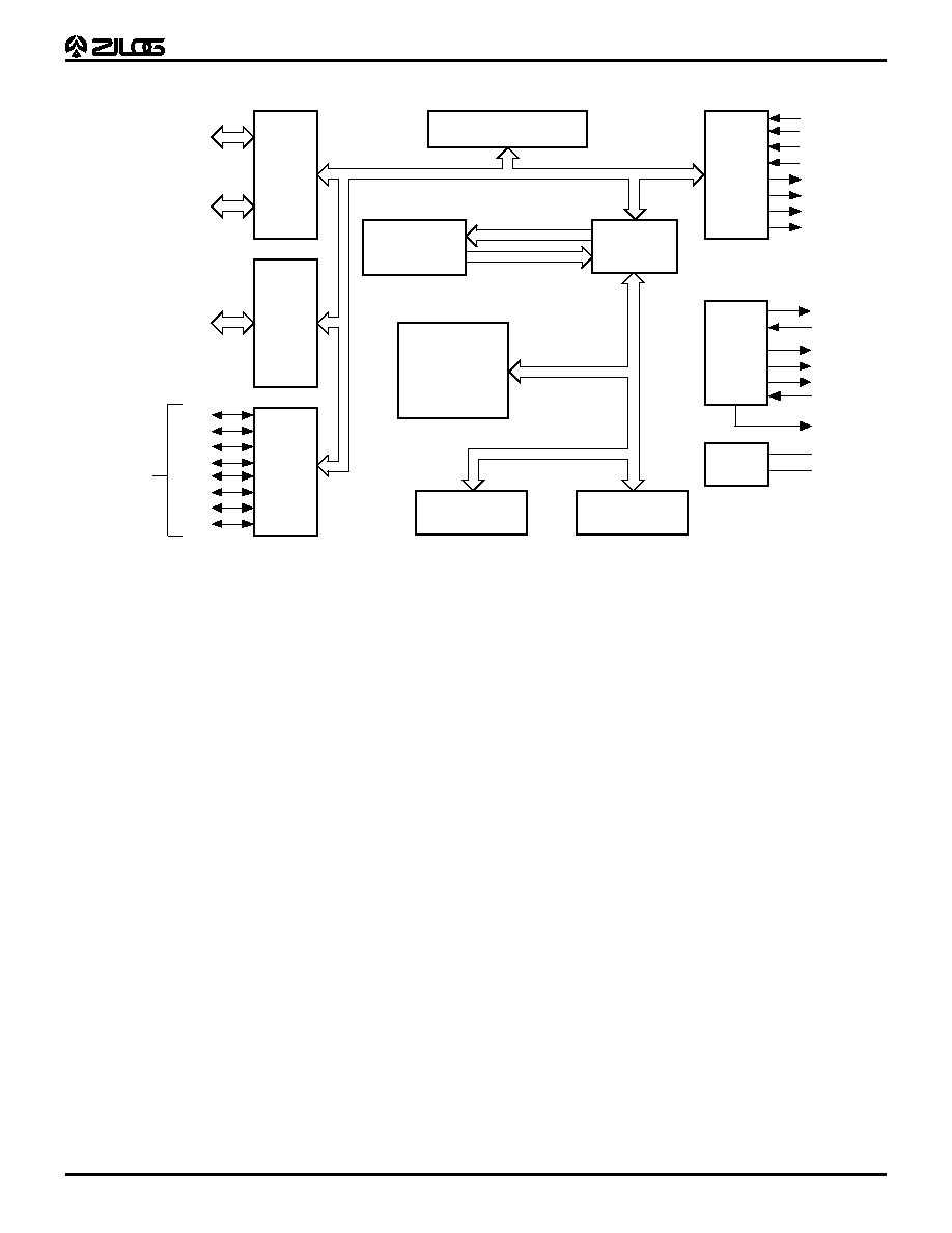
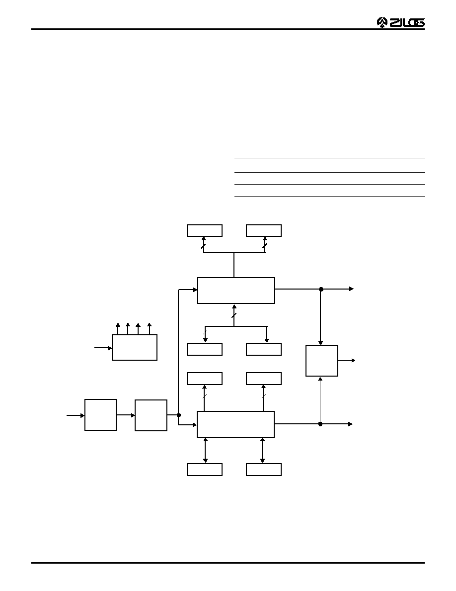
with 8-bit and 16-bit counter/timers (Figure 1). Also includ-
ed are a large number of user-selectable modes, and two
on-board comparators to process analog signals with sep-
arate reference voltages (Figure 2).
Notes:
All Signals with a preceding front slash, "/", are ac-
tive Low, e.g., B//W (WORD is active Low); /B/W (BYTE is
active Low, only).
Power connections follow conventional descriptions be-
low:
Connection
Circuit
Device
Power
V
CC
V
DD
Ground
GND
V
SS
Figure 1. Counter/Timers Diagram
HI16
LO16
16-Bit
T16
TC16H
TC16L
HI8
LO8
And/Or
Logic
Clock
Divider
Glitch
Filter
Edge
Detect
Circuit
8-Bit
T8
TC8H
TC8L
8
8
16
8
Input
SCLK
1 2 4
8
Timer 16
Timer 8/16
Timer 8
8
8
8
8
8