 | –≠–ª–µ–∫—Ç—Ä–æ–Ω–Ω—ã–π –∫–æ–º–ø–æ–Ω–µ–Ω—Ç: Z86L75 | –°–∫–∞—á–∞—Ç—å:  PDF PDF  ZIP ZIP |
DS97LVO0500
P R E L I M I N A R Y
1-1
1
P
RELIMINARY
P
RODUCT
S
PECIFICATION
Z86L70/71/75/C71
1
IR/L
OW
-V
OLTAGE
M
ICROCONTROLLER
FEATURES
s
Two Standby Modes (Typical)
≠
STOP - 2
µ
A
≠
HALT - 0.8 mA
s
Special Architecture to Automate Both Generation and
Reception of Complex Pulses or Signals:
≠
One Programmable 8-Bit Counter/Timer with Two
Capture Registers
≠
One Programmable 16-Bit Counter/Timer with
One Capture Register
≠
Programmable Input Glitch Filter for Pulse
Reception
s
Five Priority Interrupts
s
Low Voltage Detection and Protection
s
Programmable Watch-Dog/Power-On Reset Circuits
s
Two Independent Comparators with Programmable
Interrupt Polarity
s
On-Chip Oscillator that Accepts a Crystal, Ceramic
Resonator, LC, RC (mask option), or External Clock
Drive
s
Mask Selectable 200 KOhm Pull-Ups on Ports 0, 2, 3
GENERAL DESCRIPTION
The Z86L7X family of IR (Infrared)/Low-Voltage Microcon-
trollers are ROM/ROMless-based members of the Z8
Æ
MCU
single-chip family with 237/125 bytes of internal
RAM. The differentiating factor between these devices is
the availability of RAM, ROM and package options. Offer-
ing the 3V versions (Z86LXX) with the Z86C71 gives opti-
mum performance in both the low and high voltage ranges.
Zilog's CMOS Low-Voltage Microcontrollers offer fast exe-
cution, efficient use of memory, sophisticated interrupts, in-
put/output bit manipulation capabilities, automated pulse
generation/reception, and internal key-scan pull-up resis-
tors. The Z86L7X product line offers easy hardware/soft-
ware system expansion with cost-effective and low power
consumption.
The Z86L7X architecture is based on Zilog's 8-bit micro-
controller core with an Expanded Register File to allow ac-
cess to register mapped peripherals, I/O circuits, and pow-
erful counter/timer circuitry. The Z8
Æ
MCU offers a flexible
I/O scheme, an efficient register and address space struc-
ture, and a number of ancillary features that are useful in
many consumer, automotive, computer peripheral, and
battery operated hand-held applications.
There are three basic address spaces available to support
a wide range of configurations: Program Memory, Register
File, and Expanded Register File. The register file is com-
posed of 256/144 bytes of RAM. It includes four I/O port
registers, 15 control and status registers and the rest are
General-Purpose registers. The Expanded Register File
consists of two additional register groups (F and D). Exter-
nal Memory is not available on 18 and 20-pin versions.
Part
ROM
(KB)
RAM*
(Bytes)
I/O
Voltage
Ranges
Z86L70
2
125
14
2.0V to 3.9V
Z86L71
8
237
16
2.0V to 3.9V
Z86L75
4
237
14
2.0V to 3.9V
Z86C71
8
237
16
4.5V to 5.5V
Note:
*General-Purpose
Z86L70/71/75/C71
IR/Low-Voltage Microcontroller
Zilog
1-2
P R E L I M I N A R Y
DS97LVO0500
GENERAL DESCRIPTION
(Continued)
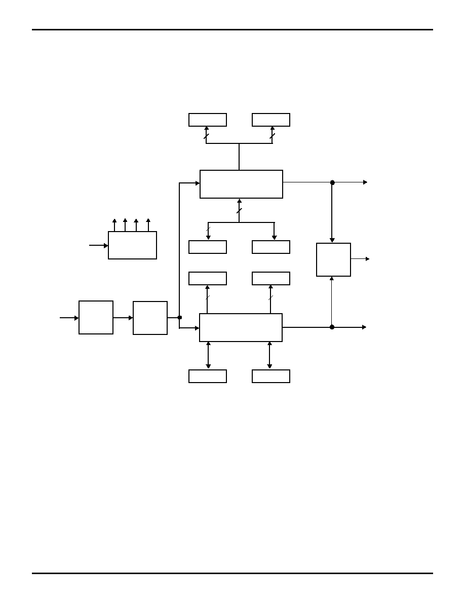
To unburden the program from coping with such real-time
problems as generating complex waveforms or receiving
and demodulating complex waveform/pulses, the Z86L7X
family offers a new intelligent counter/timer architecture
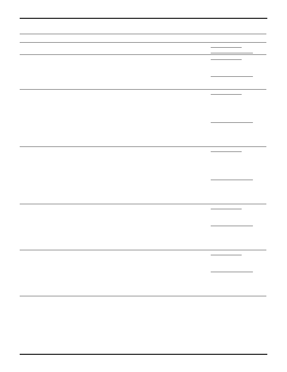
with 8-bit and 16-bit counter/timers (Figure 1). Also includ-
ed are a large number of user-selectable modes, and two
on-board comparators to process analog signals (Figure
2).
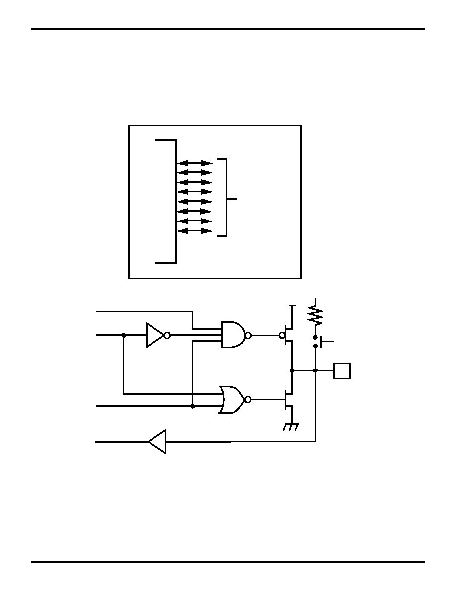
Figure 1. Counter/Timer Block Diagram
HI16
LO16
16-Bit
T16
TC16H
TC16L
HI8
LO8
And/Or
Logic
Clock
Divider
Glitch
Filter
Edge
Detect
Circuit
8-Bit
T8
TC8H
TC8L
8
8
16
8
Input
SCLK
1
2 4
8
Timer 16
Timer 8/16
Timer 8
8
8
8
8
8
Z86L70/71/75/C71
Zilog
IR/Low-Voltage Microcontroller
DS97LVO0500
P R E L I M I N A R Y
1-3
1
Note:
All Signals with a preceding front slash, "/", are ac-
tive Low, for example, B//W (WORD is active Low); /B/W
(BYTE is active Low, only).
Power connections follow conventional descriptions be-
low:
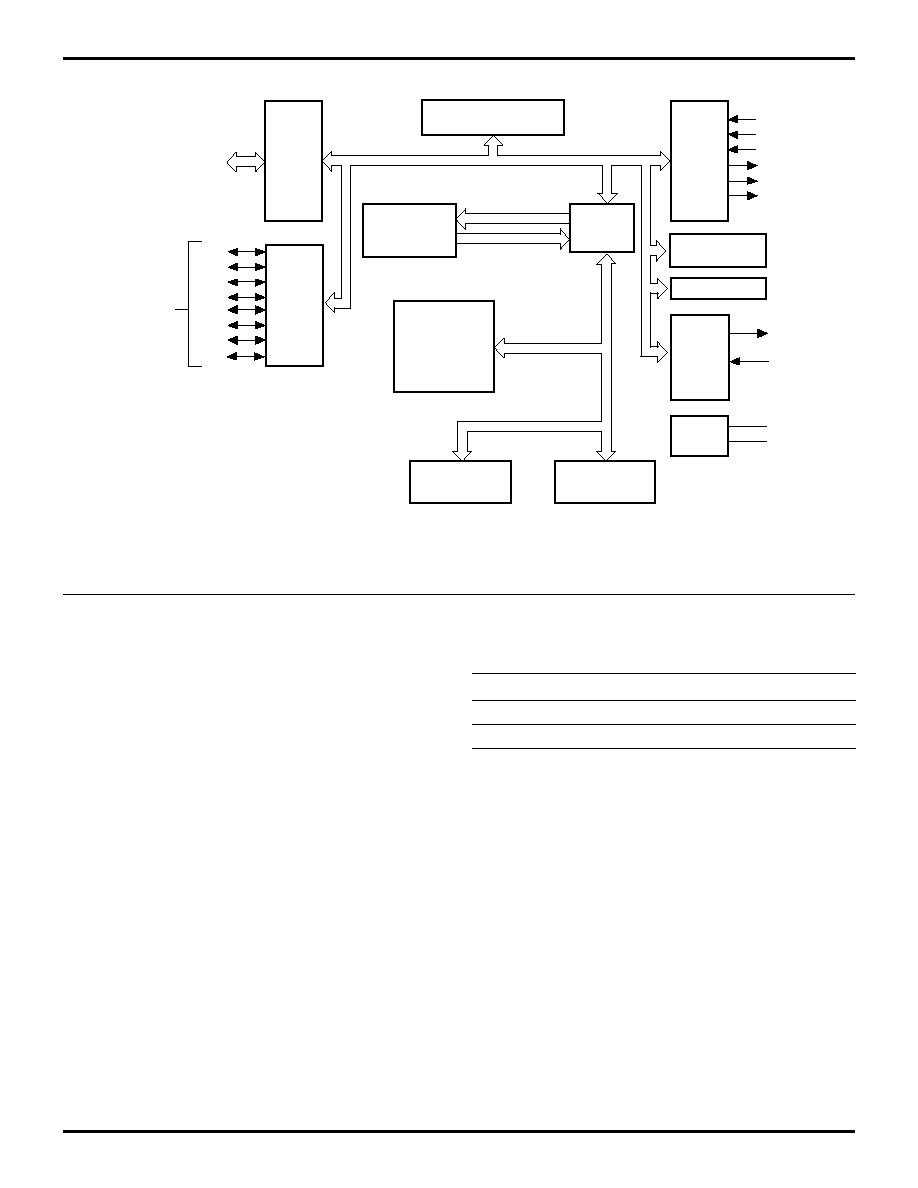
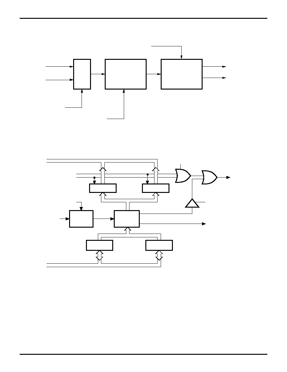
Figure 2. Functional Block Diagram
Port 0
P00
P07
P31
P32
P33
Port 3
Register File
144/256 x 8-bit
ROM
2K/4K/8K x 8
Z8 Core
Register Bus
Internal
Address Bus
Internal Data Bus
Expanded
Register
File
Expanded
Register Bus
Counter/Timer 8
8-Bit
Counter/Timer 16
16-Bit
Power
VDD
VSS
P34
P35
P36
2
P20
P21
P22
P23
P24
P25
P26
P27
Port 2
I/O Bit
Programmable
Machine
Timing
&
Instruction
Control
XTAL2
XTAL1
Two Analog
Comparators
Interrupt Control
Connection
Circuit
Device
Power
V
CC
V
DD
Ground
GND
V
SS
Z86L70/71/75/C71
IR/Low-Voltage Microcontroller
Zilog
1-4
P R E L I M I N A R Y
DS97LVO0500
PIN DESCRIPTION
Figure 3. 18-Pin DIP/SOIC Pin Assignments
P24
P25
P26
P27
VDD
XTAL2
XTAL1
P31
P32
P23
P22
P21
P20
VSS
P36
P35
P34
P33
18
Z86L70/75
DIP/SOIC
1
9
10
Figure 4. 20-Pin DIP/SOIC Pin Assignments
P24
P25
P26
P27
VDD
XTAL2
XTAL1
P31
P32
P00
P23
P22
P21
P20
VSS
P36
P35
P34
P33
P07
20
Z86L71/C71
DIP/SOIC
1
10
11
Table 1. Pin Identification
20-Pin
DIP & SOIC
18-Pin DIP
& SOIC
Symbol
Direction
Description
10
11
P00
P07
Input/Output
Input/Output
Port 0 pins are individually configurable as
input or output.
17
18
19
20
1
2
3
4
15
16
17
18
1
2
3
4
P20
P21
P22
P23
P24
P25
P26
P27
Input/Output
Input/Output
Input/Output
Input/Output
Input/Output
Input/Output
Input/Output
Input/Output
Port 2 pins are individually configurable as
input or output.
8
9
12
13
14
15
8
9
10
11
12
13
P31
P32
P33
P34
P35
P36
Input
Input
Input
Output
Output
Output
IRQ2/Modulator Input
IRQ0
IRQ1
T8 output
T16 output
T8/T16 output
7
6
5
16
7
6
5
14
XTAL1
XTAL2
V
DD
V
SS
Input
Output
Crystal, Oscillator Clock
Crystal, Oscillator Clock
Power Supply
Ground
Z86L70/71/75/C71
Zilog
IR/Low-Voltage Microcontroller
DS97LVO0500
P R E L I M I N A R Y
1-5
1
ABSOLUTE MAXIMUM RATINGS
Stresses greater than those listed under Absolute Maxi-
mum Ratings may cause permanent damage to the de-
vice. This is a stress rating only; operation of the device at
any condition above those indicated in the operational sec-
tions of these specifications is not implied. Exposure to ab-
solute maximum rating conditions for an extended period
may affect device reliability.
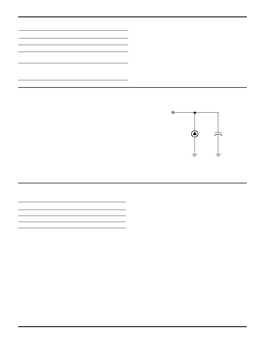
STANDARD TEST CONDITIONS
The characteristics listed below apply for standard test
conditions as noted. All voltages are referenced to GND.
Positive current flows into the referenced pin (Figure 5).
CAPACITANCE
T
A
= 25
∞
C, V
CC
= GND = 0V, f = 1.0 MHz, unmeasured pins returned to GND.
Symbol
Description
Min
Max
Units
V
CC
Supply Voltage (*)
-0.3
+7.0
V
T
STG
Storage Temp.
-65
∞
+150
∞
C
T
A
Oper. Ambient
Temp.
C
Notes:
* Voltage on all pins with respect to GND.
See Ordering Information
Figure 5. Test Load Diagram
From Output
Under Test
150 pF
I
Parameter
Max
Input capacitance
12 pF
Output capacitance
12 pF
I/O capacitance
12 pF

Z86L70/71/75/C71
IR/Low-Voltage Microcontroller
Zilog
1-6
P R E L I M I N A R Y
DS97LVO0500
DC CHARACTERISTICS (Z86L70/71/75 LOW VOLTAGE SPECIFICATIONS)
Preliminary
T
A
= 0
∞
C to +70
∞
C
Typ @
Sym
Parameter
V
CC
Min
Max
25
∞
C
Units
Conditions
Notes
Max Input Voltage
2.0V
3.9V
7
7
V
V
I
IN
<250
µ
A
I
IN
<250
µ
A
V
CH
Clock Input
High Voltage
2.0V
3.9V
0.8 V
CC
0.8 V
CC
V
CC
+ 0.3
V
CC
+ 0.3
V
V
Driven by External
Clock Generator
Driven by External
Clock Generator
V
CL
Clock Input
Low Voltage
2.0V
3.9V
V
SS
≠ 0.3
V
SS
≠ 0.3
0.2 V
CC
0.2 V
CC
V
V
Driven by External
Clock Generator
Driven by External
Clock Generator
V
IH
Input High Voltage
2.0V
3.9V
0.7 V
CC
0.7 V
CC
V
CC
+ 0.3
V
CC
+ 0.3
0.5V
CC
0.5V
CC
V
V
V
IL
Input Low Voltage
2.0V
3.9V
V
SS
≠ 0.3
V
SS
≠ 0.3
0.2 V
CC
0.2 V
CC
0.5V
CC
0.5V
CC
V
V
V
OH1
Output High
Voltage
2.0V
3.9V
V
CC
≠ 0.4
V
CC
≠ 0.4
1.7
3.7
V
V
I
OH
= ≠0.5 mA
I
OH
= ≠0.5 mA
V
OH2
Output High
Voltage (P36,
P37,P00, P01)
2.0V
3.9V
V
CC
- 0.8
V
CC
- 0.8
V
V
I
OH
= ≠7 mA
I
OH
= ≠7 mA
V
OL1
Output Low
Voltage
2.0V
3.9V
0.4
0.4
0.1
0.2
V
V
I
OL
= 1.0 mA
I
OL
= 4.0 mA
V
OL2*
Output Low
Voltage
2.0V
3.9V
0.8
0.8
0.5
0.3
V
V
I
OL
= 5.0 mA
I
OL
= 7.0 mA
V
OL2
Output Low
Voltage(P36,
P37,P00,P01)
2.0V
3.9V
0.8
0.8
0.3
0.2
V
V
I
OL
= 10 mA
I
OL
= 10 mA
V
RH
Reset Input
High Voltage
2.0V
3.9V
0.8 V
CC
0.8 V
CC
V
CC
V
CC
1.5
2.0
V
V
V
Rl
Reset Input
Low Voltage
2.0V
3.9V
V
SS
≠ 0.3
V
SS
≠ 0.3
0.2 V
CC
0.2 V
CC
0.5
0.9
V
V
V
OFFSET
Comparator Input
Offset Voltage
2.0V
3.9V
25
25
10
10
mV
mV
I
IL
Input Leakage
2.0V
3.9V
-1
-1
1
1
< 1
< 1
µ
A
µ
A
V
IN
= O
V
, V
CC
V
IN
= O
V
, V
CC
I
OL
Output Leakage
2.0V
3.9V
≠1
≠1
1
1
< 1
< 1
µ
A
µ
A
V
IN
= O
V
, V
CC
V
IN
= O
V
, V
CC
I
IR
Reset Input Pull-
Up Current
2.0V
3.9V
≠230
≠400
-50
≠90
µ
A
µ
A
V
IN
= O
V
V
IN
= O
V
I
CC
Supply Current
2.0V
3.9V
2.0V
3.9V
10
15
250
850
4
10
100
500
mA
mA
µ
A
µ
A
@ 8.0 MHz
@ 8.0 MHz
@ 32 kHz
@ 32 kHz
1,2
1,2
1,2,8

Z86L70/71/75/C71
Zilog
IR/Low-Voltage Microcontroller
DS97LVO0500
P R E L I M I N A R Y
1-7
1
T
A
= 0
∞
C to +70
∞
C
Typ @
Sym
Parameter
V
CC
Min
Max
25
∞
C
Units
Conditions
Notes
I
CC1
Standby Current
(WDT Off)
2.0V
3.9V
3
5
1
4
mA
mA
HALT Mode
V
IN
= O
V
, V
CC
@
8.0 MHz
HALT Mode
V
IN
= O
V
, V
CC
@ 8.0 MHz
1,2
1,2
2.0V
3.9V
2
4
0.8
2.5
mA
mA
Clock Divide-by-
16 @ 8.0 MHz
Clock Divide-by-
16 @ 8.0 MHz
1,2
1,2
I
CC2
Standby Current
2.0V
3.9V
2.0V
3.9V
8
10
500
800
2
3
310
600
µ
A
µ
A
µ
A
µ
A
STOP Mode
V
IN
= O
V
, V
CC
WDT is not
Running
STOP Mode
V
IN
= O
V
, V
CC
WDT is not
Running
STOP Mode
V
IN
= O
V
, V
CC
WDT is Running
3,5
3,5
3,5
V
ICR
Input Common Mode
Voltage Range
2.0V
3.9V
0
0
V
CC
- 1.0V
V
CC
- 1.0V
V
V
8
T
POR
Power-On Reset
2.0V
3.9V
12
5
75
20
18
7
ms
ms
V
RAM
Static RAM Data
Retention Voltage
Vram
0.8
0.5
V
6
V
LV
V
CC
Low Voltage
Protection
2.15
1.7
V
8 MHz max
Ext. CLK Freq.
4
Notes:
I
CC1
Crystal/Resonator
External Clock Drive
Typ
3.0 mA
0.3 mA
Max
5
5
Unit
mA
mA
Frequency
8.0 MHz
8.0 MHz
1. All outputs unloaded, inputs at rail.
2. CL1 = CL2 = 100 pF
3. Same as note [4] except inputs at V
CC
.
4. The V
LV
increases as the temperature decreases.
5. Oscillator stopped
6. Oscillator stops when V
CC
falls below V
LV
limit.
7. 32 kHz clock driver input.
8. For analog comparator, inputs when analog comparators are enabled.
* All Outputs excluding P00, P01, P36, and P37.

Z86L70/71/75/C71
IR/Low-Voltage Microcontroller
Zilog
1-8
P R E L I M I N A R Y
DS97LVO0500
DC CHARACTERISTICS (Z86C71 SPECIFICATIONS)
Preliminary
T
A
= 0
∞
C to +70
∞
C
Typ @
Sym
Parameter
V
CC
Min
Max
25
∞
C
Units
Conditions
Notes
Max Input
Voltage
4.5V
5.5V
7
7
V
V
I
IN
250
µ
A
I
IN
250
µ
A
V
CH
Clock Input
High Voltage
4.5V
5.5V
0.9 V
CC
0.9 V
CC
V
CC
+ 0.3
V
CC
+ 0.3
V
Driven by
External Clock
Generator
V
CL
Clock Input
Low Voltage
4.5V
5.5V
V
SS
≠ 0.3
V
SS
≠0.3
0.2 V
CC
0.2 V
CC
V
Driven by
External Clock
Generator
V
IH
Input High
Voltage
4.5V
5.5V
0.7 V
CC
0.7 V
CC
V
CC
+ 0.3
V
CC
+ 0.3
0.5V
CC
0.5V
CC
V
Driven by
External Clock
Generator
V
IL
Input Low
Voltage
4.5V
5.5V
V
SS
≠ 0.3
V
SS
≠ 0.3
0.5V
CC
0.5V
CC
V
V
OH1
Output High
Voltage
4.5V
5.5V
V
CC
≠ 0.4
V
CC
≠ 0.4
4.4
5.4
V
I
OH
= ≠0.5 mA
I
OH
= ≠0.5 mA
V
OH2
Output High
Voltage
(P36, P37)
4.5V
5.5V
V
CC
≠ 0.8
V
CC
≠ 0.8
V
V
I
OH
= ≠7 mA
I
OH
= ≠7 mA
V
OL1
Output Low
Voltage
4.5V
5.5V
0.4
0.4
0.1
0.2
V
V
I
OL
= 1.0 mA
I
OL
= 4.0 mA
V
OL2*
Output Low
Voltage
4.5V
3.9 V
0.8
0.8
0.3
0.4
V
V
I
OL
= 5.0 mA
I
OL
= 7.0 mA
V
OL2
Output Low
Voltage
(P00, P01,
P36,P37)
4.5V
5.5V
0.8
0.8
0.3
0.2
V
I
OL
= 10 mA
V
RH
Reset Input
High Voltage
4.5V
5.5V
0.8 V
CC
0.8 V
CC
V
CC
V
CC
2.5
3.0
V
V
V
Rl
Reset Input
Low Voltage
4.5V
5.5V
V
SS
≠ 0.3
V
SS
≠ 0.3
0.2 V
CC
0.2 V
CC
0.5
0.9
V
OFFSET
Comparator
Input
Offset Voltage
4.5V
5.5V
25
25
10
10
mV
mV
I
IL
Input Leakage
4.5V
5.5V
-1
-1
1
1
<1
<1
µ
A
µ
A
V
IN
= O
V
, V
CC
V
IN
= O
V
, V
CC
I
OL
Output Leakage
4.5V
5.5V
-1
-1
1
1
<1
<1
µ
A
µ
A
V
IN
= O
V
, V
CC
V
IN
= O
V
, V
CC
I
IR
Reset Input
Current
4.5V
5.5V
-500
-800
µ
A
µ
A
I
CC
Supply Current
4.5V
5.5V
20
30
mA
mA
@8.0 MHz
@8.0 MHz
1,2
1.2
WDT Off
4.5V
5.5V
1000
1250
10
10
µ
A
µ
A
@ 32 kHz
@ 32 kHz
1,2,8
1,2,8

Z86L70/71/75/C71
Zilog
IR/Low-Voltage Microcontroller
DS97LVO0500
P R E L I M I N A R Y
1-9
1
T
A
= 0
∞
C to +70
∞
C
Typ @
Sym
Parameter
V
CC
Min
Max
25
∞
C
Units
Conditions
Notes
I
CC1
Standby Current
(WDT Off)
4.5V
5.5V
6
8
2
5
mA
mA
HALT Mode
V
IN
= O
V
, V
CC
@
8.0 MHz
HALT Mode
V
IN
= O
V
, V
CC
@ 8.0 MHz
1,2
1,2
4.5V
5.5V
5
7
1.0
3.0
mA
mA
Clock Divide-by-
16 @ 8.0 MHz
Clock Divide-by-
16 @ 8.0 MHz
1,2
1,2
I
CC2
Standby Current
4.5V
5.5V
8
10
2
3
µ
A
µ
A
STOP Mode
V
IN
= O
V
, V
CC
WDT is not
Running
STOP Mode
V
IN
= O
V
, V
CC
WDT is not
Running
3,5
3,5
4.5V
5.5V
500
800
310
600
µ
A
µ
A
STOP Mode
V
IN
= O
V
, V
CC
WDT is Running
3,5
V
ICR
Input Common Mode
Voltage Range
2.0V
3.9V
0
0
V
CC
- 1.0V
V
CC
- 1.0V
V
V
8
T
POR
Power-On Reset
4.5V
5.5V
5.0
4.0
75
20
8.0
6.0
ms
ms
V
RAM
Static RAM Data
Retention Voltage
V
RAM
0.8
0.5
V
6
V
LV
V
CC
Low Voltage
Protection
2.15
1.7
V
8 MHz max
Ext. CLK Freq.
4
Notes:
I
CC1
Crystal/Resonator
External Clock Drive
Typ
3.5 mA
0.8 mA
Max
5
5
Unit
mA
mA
Frequency
8.0 MHz
8.0 MHz
1. All outputs unloaded, inputs at rail.
2. CL1 = CL2 = 100 pF
3. Same as note [4] except inputs at V
CC
.
4. The V
LV
increases as the temperature decreases.
5. Oscillator stopped
6. Oscillator stops when V
CC
falls below V
LV
limit.
7. 32 kHz clock driver input
8. For analog comparator, inputs when analog comparators are enabled.
* All Outputs excluding P00, P01, P36, and P37.
Z86L70/71/75/C71
IR/Low-Voltage Microcontroller
Zilog
1-10
P R E L I M I N A R Y
DS97LVO0500
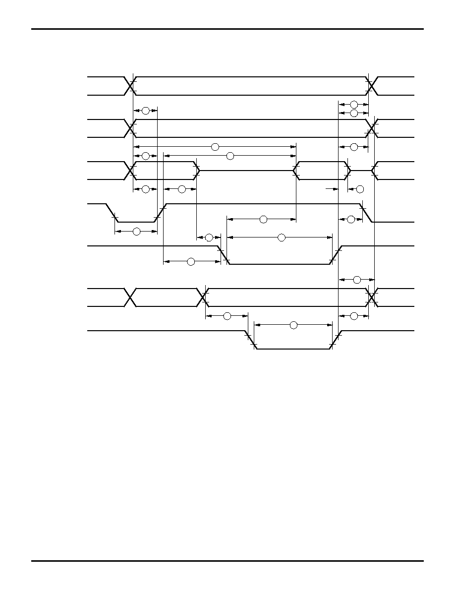
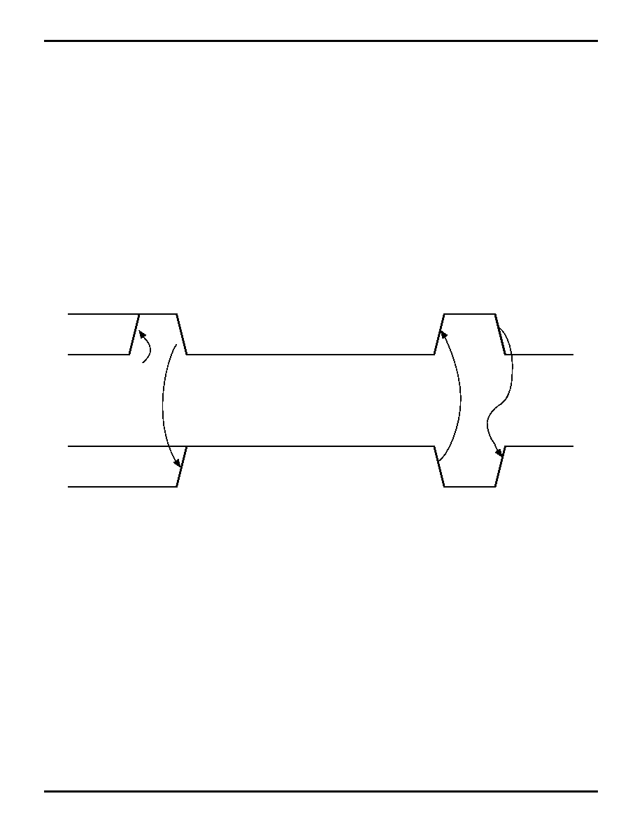
AC CHARACTERISTICS
External I/O or Memory Read and Write Timing Diagram
Figure 6. External I/O or Memory Read/Write Timing
R//W
9
12
18
3
16
13
4
5
8
11
6
17
10
15
14
2
1
Port 0, /DM
Port 1
/AS
/DS
(Read)
Port 1
/DS
(Write)
A7 - A0
D7 - D0 IN
D7 - D0 OUT
A7 - A0
19
20
7

Z86L70/71/75/C71
Zilog
IR/Low-Voltage Microcontroller
DS97LVO0500
P R E L I M I N A R Y
1-11
1
AC CHARACTERISTICS
External I/O or Memory Read and Write Timing Table
T
A
= 0
∞
C to +70
∞
C
8.0 MHz
No
Symbol
Parameter
V
CC
Min
Max
Units
Notes
1
TdA(AS)
Address Valid to /AS
Rising Delay
2.0V
3.9V
55
55
ns
ns
2
2
TdAS(A)
/AS Rising to Address
Float Delay
2.0V
3.9V
70
70
ns
ns
2
3
TdAS(DR)
/AS Rising to Read
Data Required Valid
2.0V
3.9V
400
400
ns
ns
1,2
4
TwAS
/AS Low Width
2.0V
3.9V
80
80
ns
ns
2
5
Td
Address Float to /DS
Falling
2.0V
3.9V
0
0
ns
ns
6
TwDSR
/DS (Read) Low Width
2.0V
3.9V
300
300
ns
ns
1,2
7
TwDSW
/DS (Write) Low Width
2.0V
3.9V
165
165
ns
ns
1,2
8
TdDSR(DR)
/DS Falling to Read
Data Required Valid
2.0V
3.9V
260
260
ns
ns
1,2
9
ThDR(DS)
Read Data to
/DS Rising Hold Time
2.0V
3.9V
0
0
ns
ns
2
10
TdDS(A)
/DS Rising to Address
Active Delay
2.0V
3.9V
85
85
ns
ns
2
11
TdDS(AS)
/DS Rising to /AS
2.0V
3.9V
60
70
ns
ns
2
12
TdR/W(AS)
R//W Valid to /AS
Rising Delay
2.0V
3.9V
70
70
ns
ns
2
13
TdDS(R/W)
/DS Rising to
R//W Not Valid
2.0V
3.9V
70
70
ns
ns
2
14
TdDW(DSW)
Write Data Valid to
/DS Falling (Write)
Delay
2.0V
3.9V
80
80
ns
ns
2
15
TdDS(DW)
/DS Rising to Write
Data Not Valid Delay
2.0V
3.9V
70
80
ns
ns
2
16
TdA(DR)
Address Valid to Read
Data Required Valid
2.0V
3.9V
475
475
ns
ns
1,2
17
TdAS(DS)
/AS Rising to /DS
Falling Delay
2.0V
3.9V
100
100
ns
ns
2
18
TdM(AS)
/DM Valid to /AS
Falling Delay
2.0V
3.9V
55
55
ns
ns
2
19
TdDS(DM)
/DS Rise to /DM Valid
Delay
2.0V
3.9V
70
70
ns
ns
20
ThDS(A)
/DS Rise to Address
Valid Hold Time
2.0V
3.9V
70
70
ns
ns
Notes:
1. When using extended memory timing add 2 TpC.
2. Timing numbers given are for minimum TpC.
Standard Test Load
All timing references use 0.9 V
CC
for a logic 1 and 0.1 V
CC
for a logic 0.
Z86L70/71/75/C71
IR/Low-Voltage Microcontroller
Zilog
1-12
P R E L I M I N A R Y
DS97LVO0500
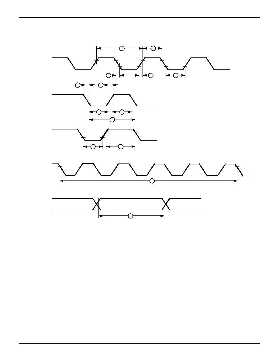
AC CHARACTERISTICS
Additional Timing Diagram
Figure 7. Additional Timing
Clock
1
3
4
8
2
2
3
T
IRQ
IN
N
6
5
7
7
Clock
Setup
10
9
Stop
Mode
Recovery
Source
11

Z86L70/71/75/C71
Zilog
IR/Low-Voltage Microcontroller
DS97LVO0500
P R E L I M I N A R Y
1-13
1
AC CHARACTERISTICS
Additional Timing Table
T
A
= 0
∞
C to +70
∞
C
8.0 MHz
No
Symbol
Parameter
V
CC
Min
Max
Units
Notes
1
TpC
Input Clock Period
2.0V
3.9V
121
121
DC
DC
ns
ns
1
1
2
TrC, TfC
Clock Input Rise and
Fall Times
2.0V
3.9V
25
25
ns
ns
1
1
3
TwC
Input Clock Width
2.0V
3.9V
37
37
ns
ns
1
1
4
TwTinL
Timer Input Low
Width
2.0V
3.9V
100
70
ns
ns
1
1
5
TwTinH
Timer Input High
Width
2.0V
3.9V
3TpC
3TpC
1
1
6
TpTin
Timer Input Period
2.0V
3.9V
8TpC
8TpC
1
1
7
TrTin, TfTin
Timer Input Rise
2.0V
3.9V
100
100
ns
ns
1
1
8A
TwIL
Interrupt Request
Low Time
2.0V
3.9V
100
70
ns
ns
1,2
1,2
8B
TwIL
Int. Request Low
Time
4.5V
5.5V
5TpC
5TpC
1,3
1,3
9
TwIH
Interrupt Request
Input High Time
4.5V
5.5V
5TpC
5TpC
1,2
1,2
10
Twsm
Stop-Mode
Recovery Width
Spec
2.0V
3.9V
2.0V
12
12
5TpC
5TpC
ns
ns
8
8
7
7
11
Tost
Oscillator Start-up
Time
2.0V
3.9V
5TpC
5TpC
4
4
12
Twdt
Watch-Dog Timer
Delay Time
(5 ms)
2.0V
3.9V
12
5
75
20
ms
ms
D0=0, 5
D1=0, 5
10 ms
2.0V
3.9V
20
10
150
40
ms
ms
D0=1, 5
D1=0, 5
20 ms
2.0V
3.9V
50
20
300
80
ms
ms
D0=1, 5
D1=0, 5
80 ms
2.0V
3.9V
225
80
1200
320
ms
ms
D0=1, 5
D1=0, 5
Notes:
1. Timing Reference uses 0.9 V
CC
for a logic 1 and 0.1 V
CC
for a logic 0.
2. Interrupt request through Port 3 (P33-P31).
3. Interrupt request through Port 3 (P30).
4. SMR - D5 = 0
5. Reg. WDTMR
6. Reg. SMR - D5 = 0
7. Reg. SMR - D5 = 1
Z86L70/71/75/C71
IR/Low-Voltage Microcontroller
Zilog
1-14
P R E L I M I N A R Y
DS97LVO0500
PIN FUNCTIONS
XTAL1 Crystal 1 (time-based input). This pin connects a
parallel-resonant crystal, ceramic resonator, LC, or RC
network or an external single-phase clock to the on-chip
oscillator input.
XTAL2 Crystal 2 (time-based output). This pin connects a
parallel-resonant, crystal, ceramic resonant, LC, or RC
network to the on-chip oscillator output.
Port 0 (P07-P00). Port 0 is an two-bit, bidirectional,
CMOS-compatible port. These I/O lines are configured un-
der software control as an I/O port. The output drivers are
push-pull.
An optional 200 KOhm pull-up is available as a mask op-
tion on both Port 0 bits.
These pull-ups are disabled when configured (bit by
bit) as an output.
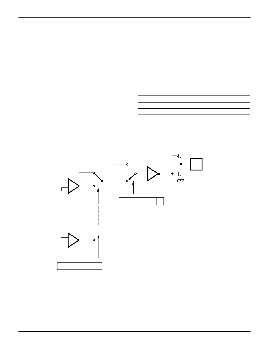
Figure 8. Port 0 Configuration
OEN
Out
In
PAD
200 K
Mask
Option
Z86L70/71/75/C71
Zilog
IR/Low-Voltage Microcontroller
DS97LVO0500
P R E L I M I N A R Y
1-15
1
Port 2 (P27-P20). Port 2 is an 8-bit, bidirectional, CMOS-
compatible I/O port. These eight I/O lines can be indepen-
dently configured under software control as inputs or out-
puts. Port 2 is always available for I/O operation. A mask
option is available to connect eight 200 KOhms (
±
50%)
pull-up resistors on this port. Bits programmed as outputs
are globally programmed as either push-pull or open-
drain. The Z8
wakes up with the eight bits of Port 2 config-
ured as inputs with open-drain outputs.
Port 2 also has an 8-bit input OR and an AND gate which
can be used to wake up the part from STOP Mode (Figure
33). P20 can be programmed to access the edge selection
circuitry (Figure 9).
Figure 9. Port 2 Configuration
Open-Drain
OEN
Out
In
PAD
Port 2 (I/O)
Z86LXX
MCU
VCC
Mask
Option
200 K
Z86L70/71/75/C71
IR/Low-Voltage Microcontroller
Zilog
1-16
P R E L I M I N A R Y
DS97LVO0500
PIN FUNCTIONS (Continued)
Port 3 (P36-P31). Port 3 is a 6-bit, CMOS-compatible
three fixed input and three fixed output port. Port 3 consists
of three fixed input (P33-P31) and three fixed output (P36-
P34), and can be configured under software control for In-
put/Output, Interrupt, and output from the counter/timers.
P31, P32, and P33 are standard CMOS inputs; outputs are
push-pull, except for P34, P35 which have floating drain
capability (controlled by P3M, D0).
Two on-board comparators process analog signals on P31
and P32 with reference to the voltage on P33. The analog
function is enabled by programming the Port 3 Mode Reg-
ister (bit 1). P31 and P32 are programmable as rising, fall-
ing, or both edge triggered interrupts (IRQ register bits 6
and 7). Pref1 and P33 are the comparator reference volt-
age inputs. Access to the Counter Timer edge detection
circuit is through P31 or P20 (see CTR1 description).
Port 3 provides the following control functions: three exter-
nal interrupt request signals (IRQ2-IRQ0).
Port 3 also provides output for each of the counter/timers
and the AND/OR Logic. Control is performed by program-
ming bits D5-D4 of CTRI, bit 0 of CTR0 and bit 0 of CTR2.
Table 2. Pin Assignments
Pin
I/O
C/T
Comp.
Int.
Ext
P31
IN
IN
AN1
IRQ2
P32
IN
AN2
IRQ0
P33
IN
V
REF
IRQ1
P34
OUT
T8
A01
DM
P35
OUT
T16
P36
OUT
T8/16
P20
I/O
IN
Figure 10. Port 3 Configuration
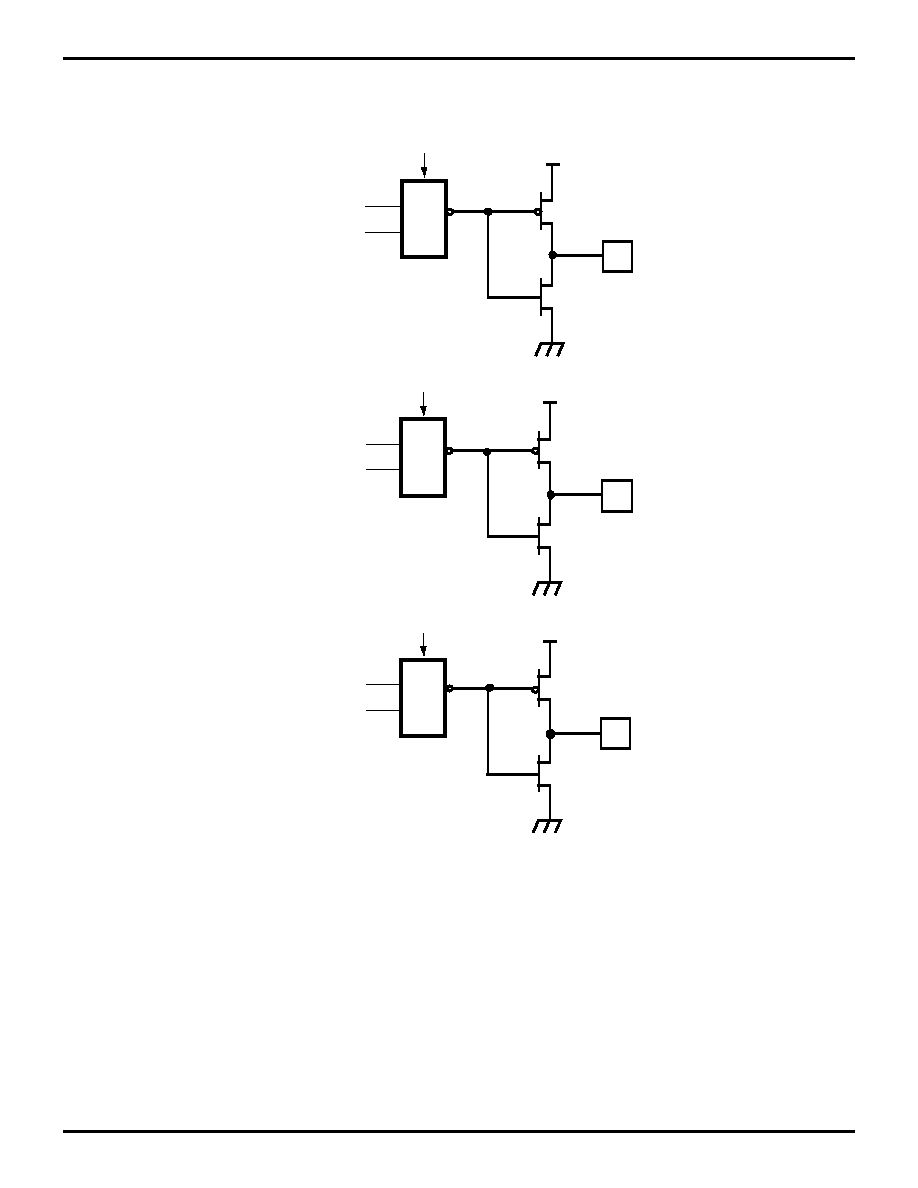
P34 OUT
P32
+
-
P33
0 = P34 Standard Output
1 = P34 Comparator Output
PCON
D0
P31
+
-
P33
P34
PAD
*
T8
P34 OUT
0 Normal Control
1 8-bit Timer output active
CTR0
D0
Counter/Timer
Reset condition.
*
Comp1
Comp2
Z86L70/71/75/C71
Zilog
IR/Low-Voltage Microcontroller
DS97LVO0500
P R E L I M I N A R Y
1-17
1
Comparator Inputs. In Analog Mode, Port 3 (P31 and
P32) have a comparator front end. P33 serves as the ref-
erence for both comparators. In this mode, the P33 internal
data latch and its corresponding IRQ1 is diverted to the
SMR Sources (excluding P31, P32, and P33) as shown in
Figure 38. In digital mode, P33 is used as D3 of the Port 3
input register which then generates IRQ1 as shown in Fig-
ure 16.
Notes: Comparators are powered down by entering STOP
Mode. For P31-P33 to be used as a Stop-Mode Recovery
source, these inputs must be placed into digital mode.
Comparator Outputs. COMP1 may be programmed to be
outputted on P34 through the PCON register (Figure 15).
Power-On Reset. the typical reset output time is 5 ms.
The Z86L7X does not reset WDTMR, SMR, P2M, or P3M
registers on a Stop-Mode Recovery operation.
Figure 11. Port 3 Configuration
Port 3
(I/O or Handshake)
Z86L7X
MCU
Pref1
P31
P32
P33
P34
P35
P36
P37
Note:
P31, 32, 33 have a 200 K
mask option
200 K
Mask
Option
D1
R247 = P3M
P31 (AN1)
P32 (AN2)
P33 (REF2)
From Stop-Mode
Recovery Source of SMR
1 = Analog
0 = Digital
IRQ2, P31 Data Latch
IRQ0, P32 Data Latch
IRQ1, P33 Data Latch
DIG.
AN.
-
+
-
+
Pref
Comp1
Comp2
Z86L70/71/75/C71
IR/Low-Voltage Microcontroller
Zilog
1-18
P R E L I M I N A R Y
DS97LVO0500
PIN FUNCTIONS (Continued)
Figure 12. Port 3 Configuration
VDD
Out 34
T8_Out
CTR0, D0
Pad
Out 35
T16_Out
CTR2, D0
Out 36
T8/16_Out
CTR1, D6
MUX
MUX
MUX
P34
VDD
Pad
P35
VDD
Pad
P36
Z86L70/71/75/C71
Zilog
IR/Low-Voltage Microcontroller
DS97LVO0500
P R E L I M I N A R Y
1-19
1
FUNCTIONAL DESCRIPTION
The Z8 incorporates special functions to enhance the Z8's
functionality in consumer and battery operated applica-
tions.
Reset. The device is reset in one of the following condi-
tions:
1.
Power-On Reset
2.
Watch-Dog Timer
3.
Stop-Mode Recovery Source
4.
Low Voltage Detection
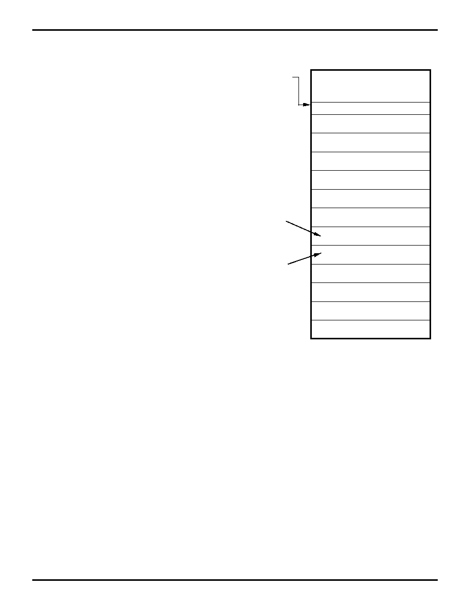
Program Memory. The Z86L7X addresses up to 2K, 4K,
8 KB of internal program memory, with the remainder be-
ing external memory (Figure 13). The first 12 bytes of pro-
gram memory are reserved for the interrupt vectors. These
locations contain five 16-bit vectors that correspond to the
five available interrupts. Addresses 12 to 2K, 4K, 8K (de-
pendent on version) consist of on-chip mask-programmed
ROM.
Figure 13. Program Memory Map
11
10
9
8
7
6
5
4
3
2
1
0
Location of
First Byte of
Instruction
Executed
After RESET
Interrupt
Vector
(Lower Byte)
Interrupt
Vector
(Upper Byte)
Reserved
IRQ4
IRQ4
IRQ3
IRQ3
IRQ2
IRQ2
IRQ1
IRQ1
IRQ0
IRQ0
Reserved
On-Chip
ROM
Reset Start Address
12

Z86L70/71/75/C71
IR/Low-Voltage Microcontroller
Zilog
1-20
P R E L I M I N A R Y
DS97LVO0500
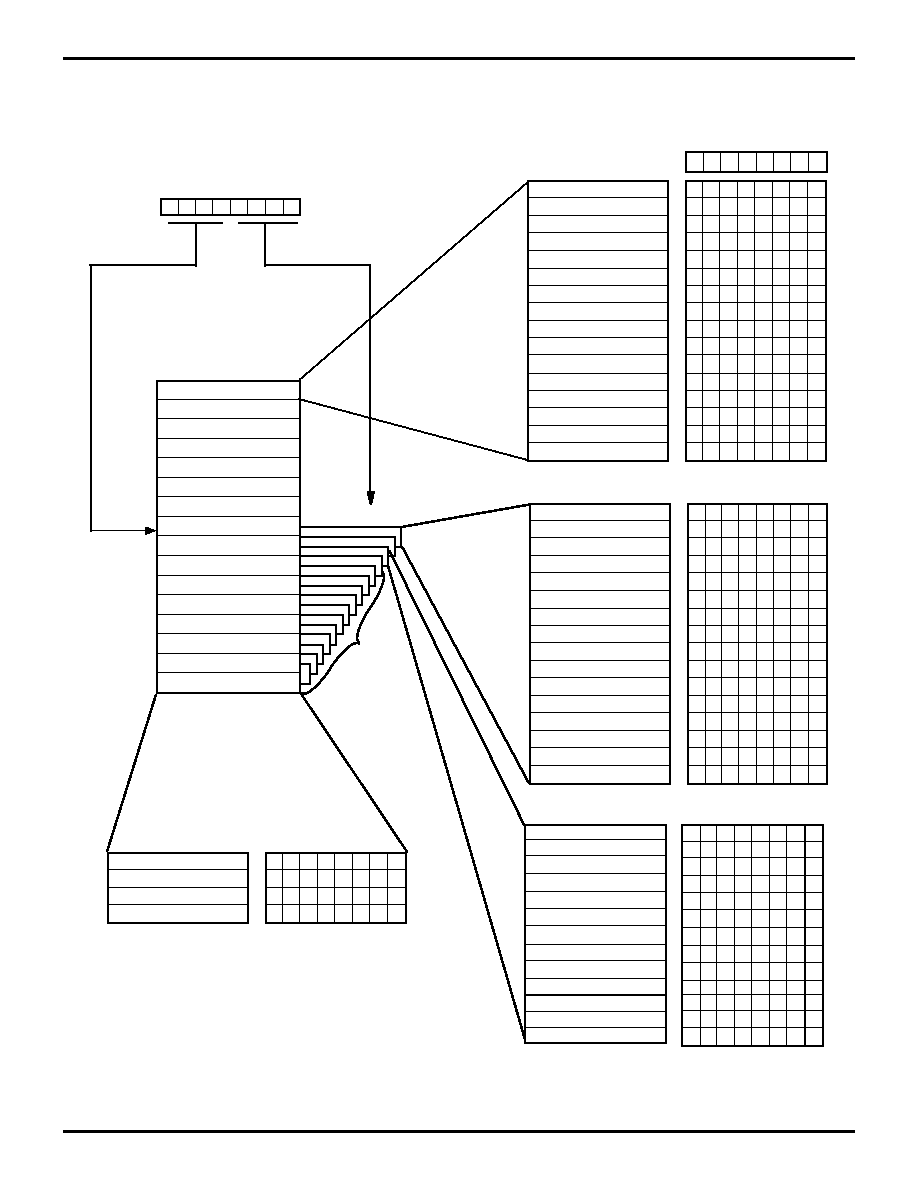
Expanded Register File. The register file has been ex-
panded to allow for additional system control registers,
and for mapping of additional peripheral devices into the
register address area. The Z8 register address space R0
through R15 has been implemented as 16 banks of 16 reg-
isters per bank. These register groups are known as the
ERF (Expanded Register File). Bits 7-4 of register RP se-
lect the working register group. Bits 3-0 of register RP se-
lect the expanded register file bank. Note that expanded
register bank is also referred to as expanded register
group (Figure14).
The upper nibble of the register pointer (Figure 23) selects
which working register group of 16 bytes in the register file,
out of the possible 256, will be accessed. The lower nibble
selects the expanded register file bank and, in the case of
the Z86LXX family, banks 0, F, and D are implemented. A
0h in the lower nibble will allow the normal register file
(bank 0) to be addressed, but any other value from 1H to
FH will exchange the lower 16 registers to an expanded
register bank.
For example:
Z86L70: (See Figure 16)
R253 RP = 00H
R0 = Port 0
R1 = Port 1
R2 = Port 2
R3 = Port 3
But if:
R253 RP = 0DH
R0 = CTRL0
R1 = CTRL1
R2 = CTRL2
R3 = Reserved
The counter/timers are mapped into ERF group D. Access
is easily done using the following example:
LD
RP, #0DH Select ERF D for access to bank D ( work-
ing register group 0)
LD
R0,#xx
load CTRL0
LD
1, #xx
load CTRL1
LD
R1, 2
CTRL2
CTRL1
LD
RP, #7DH
Select expanded register bank D and
working register group 7 of bank 0 for access .
LD
71H, 2
CTRL2
register 71H
LD
R1, 2
CTRL2
register 71H
Z86L70/71/75/C71
Zilog
IR/Low-Voltage Microcontroller
DS97LVO0500
P R E L I M I N A R Y
1-21
1
Figure 14. Expanded Register File Architecture
7
6
5
4
3
2
1
0
Working Register
Group Pointer
Expanded Register
File (Bank) Pointer
FF
FO
7F
0F
00
Z8 Register File**
REGISTER POINTER
FF
FE
FD
FC
FB
FA
F9
F8
F7
F6
F5
F4
F3
F2
F1
F0
SPL
SPH
RP
FLAGS
IMR
IRQ
IPR
P01M
P3M
P2M
U
U
0
U
0
0
U
0
0
1
(F) 0F
(F) 0E
(F) 0D
(F) 0C
(F) 0B
Reserved
(F) 01
(F) 00
WDTMR
SMR
U
U
0
U
U
0
U
1
0
1
U
U
0
U
U
0
U
0
0
1
U
U
0
U
U
0
U
0
0
1
U
U
0
U
U
0
U
1
0
1
U
U
0
U
U
0
U
1
0
1
U
U
0
U
U
0
U
0
0
1
U
U
0
U
U
0
U
1
0
1
U
U
U
0
1
1
0
1
0
0
1
0
0
0
U
0
REGISTER**
EXPANDED REG. GROUP (F)
RESET CONDITION
REGISTER**
Z8
Æ
STANDARD CONTROL REGISTERS
RESET CONDITION
D7 D6 D5 D4 D3 D2 D1 D0
Reserved
*
*
*
Reserved
SMR2
Reserved
Reserved
U
U
U
U
U
U
U
U
U
U
U
U
U
U
U
U
U
U
U
U
U
U
U
U
U
U
U
U
U
U
U
U
0
0
0
0
0
0
0
0
0
U
U
0
0
0
0
0
Reserved
PCON
U
0
*
0
U
1
1
U
U
U
U
U
U
U
U
U
U
U
U
U
U
U
U
U
U
U
U
U
U
U
U
U
U
U
U
REGISTER**
EXPANDED REG. GROUP (0)
RESET CONDITION
(0) 03
P3
(0) 02
P2
(0) 01
P1
(0) 00
P0
U = Unknown
* Will not be reset with a Stop-Mode Recovery
** All addresses are in Hexadecimal
@
*
Will not be reset with a Stop-Mode Recovery, except Bit 0.
Reserved
Reserved
Reserved
Reserved
Reserved
U
0
U
0
0
0
U
U
EXPANDED REG. GROUP (D)
REGISTER**
(D) 0C
(D) 0B
(D) 0A
(D) 09
(D) 08
(D) 07
(D) 06
(D) 05
(D) 04
(D) 03
(D) 02
Reserved
HI8
L08
HI16
L016
TC16H
TC16L
TC8H
TC8L
Reserved
CTR2
RESET CONDITION
U
U
U
U
U
U
U
U
U
U
U
U
U
U
U
U
U
U
0
U
U
U
U
U
U
U
U
U
U
U
U
U
U
U
U
U
U
U
U
U
U
U
U
U
U
U
U
U
U
U
U
U
U
U
U
U
U
U
U
U
U
U
U
U
U
U
U
U
U
U
U
U
(D) 01 CTR1
(D) 00 CTR0
U
U
U
U
U
U
U
U
0
U
U
U
U
U
U
Reserved
U
U
U
U
U
U
U
Reserved
Reserved
Reserved
Reserved
Reserved
Reserved
Reserved
Reserved
@ P36 is set to an unknown state upon SMR Reset. Rest of
ports will not be affected.
Z86L70/71/75/C71
IR/Low-Voltage Microcontroller
Zilog
1-22
P R E L I M I N A R Y
DS97LVO0500
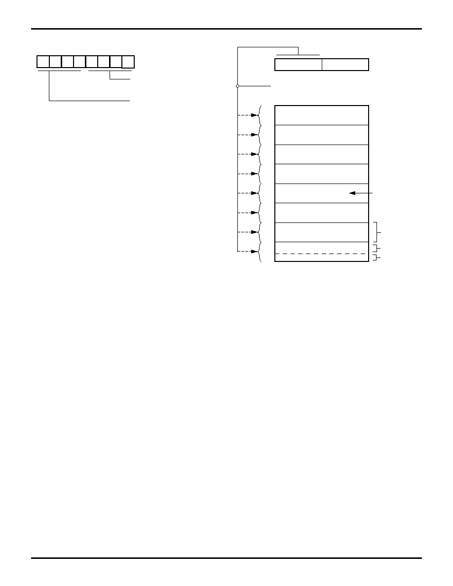
RAM/Register File. The register file (group 0) consists of
four I/O port registers, 236 general purpose registers, and
16 control and status registers (R0-R3, R4-R239, and
R240-R255, respectively), plus two expanded registers
group (Banks D and F). In the 4-bit mode, the register file
is divided into 16 working register groups, each occupying
16 continuous locations. The Register Pointer addresses
the starting location of the active working register group.
Note: Registers E0-EF of Bank 0 are only accessed
through working registers and indirect addressing modes.
Stack. The Z86L7X internal register file is used for the
stack. An 8-bit Stack Pointer (R255) is used for the internal
stack that resides in the general-purpose registers (R4-
R239).
Figure 15. Register Pointer
D7 D6 D5 D4 D3 D2 D1 D0
Expanded Register Bank
File Pointer
Working Register
Pointer
R253 RP
Default Setting After
Reset = 0000 0000
Figure 16. Register Pointer
The upper nibble of the register file address
provided by the register pointer specifies
the active working-register group
r
7
r
6
r
5
r
4
R253
I/O Ports
Specified Working
Register Group
The lower nibble
of the register
file address
provided by the
instruction points
to the specified
register
r
3
r
2
r
1
r
0
Register Group 0
7F
Register Group 1
6F
5F
4F
3F
2F
1F
0F
00
10
20
30
40
50
60
70
R15 to R0
R15 to R4 *
R3 to R0 *
* RP = 00: Selects Register Group 0, Working Register 0.
Z86L70/71/75/C71
Zilog
IR/Low-Voltage Microcontroller
DS97LVO0500
P R E L I M I N A R Y
1-23
1
Counter/Timer Register Description
HI8(D)%0B: Holds the captured data from the output of the
8-bit Counter/Timer0. This register is typically used to hold
the number of counts when the input signal is 1.
L08(D)%0A: Holds the captured data from the output of
the 8-bit Counter/Timer0. This register is typically used to
hold the number of counts when the input signal is 0.
HI16(D)%09: Holds the captured data from the output of
the 16-bit Counter/Timer16. This register holds the MS-
Byte of the data.
L016(D)%08: Holds the captured data from the output of
the 16-bit Counter/Timer16. This register holds the LS-
Byte of the data.
TC16H(D)%07: Counter/Timer2 MS-Byte Hold Register.
TC16L(D)%06: Counter/Timer2 LS-Byte Hold Register.
TC8H(D)%05: Counter/Timer8 High Hold Register.
TC8L(D)%04: Counter/Timer8 Low Hold Register.
Expanded Register Group D
(D)%0C
Reserved
(D)%0B
HI8
(D)%0A
LO8
(D)%09
HI16
(D)%08
LO16
(D)%07
TC16H
(D)%06
TC16L
(D)%05
TC8H
(D)%04
TC8L
(D)%03
Reserved
(D)%02
CTR2
(D)%01
CTR1
(D)%00
CTR0
Field
Bit Position
Description
T8_Capture_HI
76543210
R
W
Captured Data
No Effect
Field
Bit Position
Description
T16_Capture_LO
76543210
R
W
Captured Data
No Effect
Field
Bit
Position
Description
T16_Capture_HI
76543210
R
W
Captured Data
No Effect
Field
Bit
Position
Description
T16_Capture_LO
76543210
R
W
Captured Data
No Effect
Field
Bit
Position
Description
T16_Data_HI
76543210
R
W
Data
Field
Bit
Position
Description
T16_Data_LO
76543210
R/W
Data
Field
Bit Position
Description
T8_Level_HI
76543210
R/W
Data
Field
Bit Position
Description
T8_Level_LO
76543210
R/W
Data

Z86L70/71/75/C71
IR/Low-Voltage Microcontroller
Zilog
1-24
P R E L I M I N A R Y
DS97LVO0500
CTR0 (D)00: Counter/Timer8 Control Register.
CTR0: Counter/Timer8 Control Register Description
T8 Enable. This field enables T8 when set (written) to 1.
Single/Modulo-N. When set to 0 (modulo-n), the counter
reloads the initial value when the terminal count is
reached. When set to 1 (single pass), the counter stops
when the terminal count is reached.
Time-Out. This bit is set when T8 times out (terminal count
reached). To reset this bit, a 1 should be written to this lo-
cation. This is the only way to reset this status condition,
therefore, care should be taken to reset this bit prior to us-
ing/enabling the counter/timers.
Note: Care must be taken when utilizing the OR or AND
commands to manipulate CTR0, bit 5 and CTR1, bits 0
and 1 (Demodulation Mode). These instructions use a
Read-Modify-Write sequence in which the current status
from the CTR0 and CTR1 registers will be ORed or ANDed
with the designated value and then written back into the
registers. Example: When the status of bit 5 is 1, a reset
condition will occur.
T8 Clock. Defines the frequency of the input signal to T8.
Capture_INT_Mask. Set this bit to allow interrupt when
data is captured into either LO8 or HI8 upon a positive or
negative edge detection in demodulation mode.
Counter_INT_Mask. Set this bit to allow interrupt when T8
has a time out.
P34_Out. This bit defines whether P34 is used as a normal
output pin or the T8 output.
Field
Bit Position
Value
Description
T8_Enable
7-------
R
W
0*
1
0
1
Counter Disabled
Counter Enabled
Stop Counter
Enable Counter
Single/Modulo-N
-6------
R/W
0
1
Modulo-N
Single Pass
Time_Out
--5-----
R
0
No Counter Time-Out
Counter Time-Out Occurred
No Effect
Reset Flag to 0
T8_Clock
---43---
R/W
0 0
0 1
1 0
1 1
SCLK
SCLK/2
SCLK/4
SCLK/8
Capture_INT_Mask
-----2--
R/W
0
1
Disabled Data Capture Int.
Enable Data Capture Int.
Counter_INT_Mask
------1-
R/W
0
1
Disable Data Capture Int.
Enable Time-Out Int.
P34_Out
-------0
R/W
0
1
P34 as Port Output
T8 Output on P34
Z86L70/71/75/C71
Zilog
IR/Low-Voltage Microcontroller
DS97LVO0500
P R E L I M I N A R Y
1-25
1
CTR1 (D)01: Controls the functions in common with the T8 and T16
Field
Bit Position
Value
Description
Mode
7-------
R/W
0
1
Transmit Mode
Demodulation Mode
P36_Out/
Demodulator_Input
-6------
R/W
0
1
0
1
Transmit Mode
Port Output
T8/T16 Output
Demodulation Mode
P31
P20
T8/T16_Logic/
Edge _Detect
--54----
R/W
00
01
10
11
00
01
10
11
Transmit Mode
AND
OR
NOR
NAND
Demodulation Mode
Falling Edge
Rising Edge
Both Edges
Reserved
Transmit_Submode/Glitch_
Filter
----32--
R/W
00
01
10
11
00
01
10
11
Transmit Mode
Normal Operation
Ping-Pong Mode
T16_Out=0
T16_Out=1
Demodulation Mode
No Filter
4 SCLK Cycle
8 SCLK Cycle
16 SCLK Cycle
Initial_T8_Out/
Rising_Edge
------1-
R/W
R
W
0
1
0
1
0
1
Transmit Mode
T8_OUT is 1 Initially
T8_OUT is 1 Initially
Demodulation Mode
No Rising Edge
Rising Edge Detected
No Effect
Reset Flag to 0
Initial_T16_Out/
Falling _Edge
-------0
R/W
R
W
0
1
0
1
0
1
Transmit Mode
T16_OUT is 0 Initially
T16_OUT is 1 Initially
Demodulation Mode
No Falling Edge
Falling Edge Detected
No Effect
Reset Flag to 0

Z86L70/71/75/C71
IR/Low-Voltage Microcontroller
Zilog
1-26
P R E L I M I N A R Y
DS97LVO0500
CTR1 Register Description
Mode. If it is 0, the Counter/Timers are in the transmit
mode, otherwise they are in the demodulation mode.
P36_Out/Demodulator_Input. In Transmit Mode, this bit
defines whether P36 is used as a normal output pin or the
combined output of T8 and T16.
In Demodulation Mode, this bit defines whether the input
signal to the Counter/Timers is from P20 or P31.
T8/T16_Logic/Edge _Detect. In Transmit Mode, this field
defines how the outputs of T8 and T16 are combined
(AND, OR, NOR, NAND).
In Demodulation Mode, this field defines which edge
should be detected by the edge detector.
Transmit_Submode/Glitch Filter. In Transmit Mode, this
field defines whether T8 and T16 are in the "Ping-Pong"
mode or in independent normal operation mode. Setting
this field to "Normal Operation Mode" terminates the "Ping-
Pong Mode" operation. When set to 10, T16 is immediately
forced to a 0. When set to 11, T16 is immediately forced to
a 1.
In Demodulation Mode, this field defines the width of the
glitch that should be filtered out.
Initial_T8_Out/Rising_Edge. In Transmit Mode, if 0, the
output of T8 is set to 0 when it starts to count. If 1, the out-
put of T8 is set to 1 when it starts to count. When this bit is
set to 1 or 0, T8_OUT will be set to the opposite state of
this bit. This insures that when the clock is enabled a tran-
sition occurs to the initial state set by CTR1, D1.
In Demodulation Mode, this bit is set to 1 when a rising
edge is detected in the input signal. In order to reset it, a 1
should be written to this location.
Initial_T16 Out/Falling _Edge. In Transmit Mode, if it is 0,
the output of T16 is set to 0 when it starts to count. If it is
1, the output of T16 is set to 1 when it starts to count. This
bit is effective only in Normal or Ping-Pong Mode (CTR1,
D3, D2). When this bit is set, T16_OUT will be set to the
opposite state of this bit. This insures that when the clock
is enabled a transition occurs to the initial state set by
CTR1, D0.
In Demodulation Mode, this bit is set to 1 when a falling
edge is detected in the input signal. In order to reset it, a 1
should be written to this location.
Note: Modifying CTR1, (D1 or D0) while the counters are
enabled will cause un-predictable output from T8/16_OUT.

Z86L70/71/75/C71
Zilog
IR/Low-Voltage Microcontroller
DS97LVO0500
P R E L I M I N A R Y
1-27
1
CTR2 (D)%02: Counter/Timer16 Control Register.
CTR2 Description
T16_Enable. This field enables T16 when set to 1.
Single/Modulo-N. In Transmit Mode, when set to 0, the
counter reloads the initial value when terminal count is
reached. When set to 1, the counter stops when the termi-
nal count is reached.
In Demodulation Mode, when set to 0 , T16 captures and
reloads on detection of all the edges; when set to 1, T16
captures and detects on the first edge, but ignores the sub-
sequent edges. For details, see the description of T16 De-
modulation Mode.
Time_Out. This bit is set when T16 times out (terminal
count reached). In order to reset it, a 1 should be written to
this location.
T16_Clock. Defines the frequency of the input signal to
Counter/Timer16.
Capture_INT_Mask. Set this bit to allow interrupt when
data is captured into LO16 and HI16.
Counter_INT_Mask. Set this bit to allow interrupt when
T16 times out.
P35_Out. This bit defines whether P35 is used as a normal
output pin or T16 output.
Field
Bit Position
Value
Description
T16_Enable
7-------
R
W
0*
1
0
1
Counter Disabled
Counter Enabled
Stop Counter
Enable Counter
Single/Modulo-N
-6------
R/W
0
1
0
1
Transmit Mode
Modulo-N
Single Pass
Demodulation Mode
T16 Recognizes Edge
T16 Does Not Recognize Edge
Time_Out
--5-----
R
0
1
0
1
No Counter Time-Out
Counter Time-Out Occurred
No Effect
Reset Flag to 0
T16 _Clock
---43---
R/W
00
01
10
11
SCLK
SCLK/2
SCLK/4
SCLK/8
Capture_INT_Mask
-----2--
R/W
0
1
Disable Data Capture Int.
Enable Data Capture Int.
Counter_INT_Mask
------1-
R/W
0
1
Disable Time-Out Int.
Enable Time-Out Int.
P35_Out
-------0
R/W
0
1
P35 as Port Output
T16 Output on P35
Note: * Indicates the value upon Power-On Reset

Z86L70/71/75/C71
IR/Low-Voltage Microcontroller
Zilog
1-28
P R E L I M I N A R Y
DS97LVO0500
SMR2(F)%0D: Stop-Mode Recovery Register 2.
Field
Bit Position
Value
Description
Reserved
7-------
0
Reserved (Must be 0)
Recovery Level
-6------
W
0*
1
Low
High
Reserved
--5-----
0
Reserved (Must be 0)
Source
---432--
W
000*
001
010
011
100
101
110
111
A. POR Only
B. NAND of P23-P20
C. NAND or P27-P20
D. NOR of P33-P31
E. NAND of P33-P31
F. NOR of P33-P31, P00,P07
G. NAND of P33-P31,P00,P07
H. NAND of P33-P31,P22-P20
Reserved
------10
00
Reserved (Must be 0)
Note: * Indicates the value upon Power-On Reset.
Z86L70/71/75/C71
Zilog
IR/Low-Voltage Microcontroller
DS97LVO0500
P R E L I M I N A R Y
1-29
1
Counter/Timer Functional Blocks
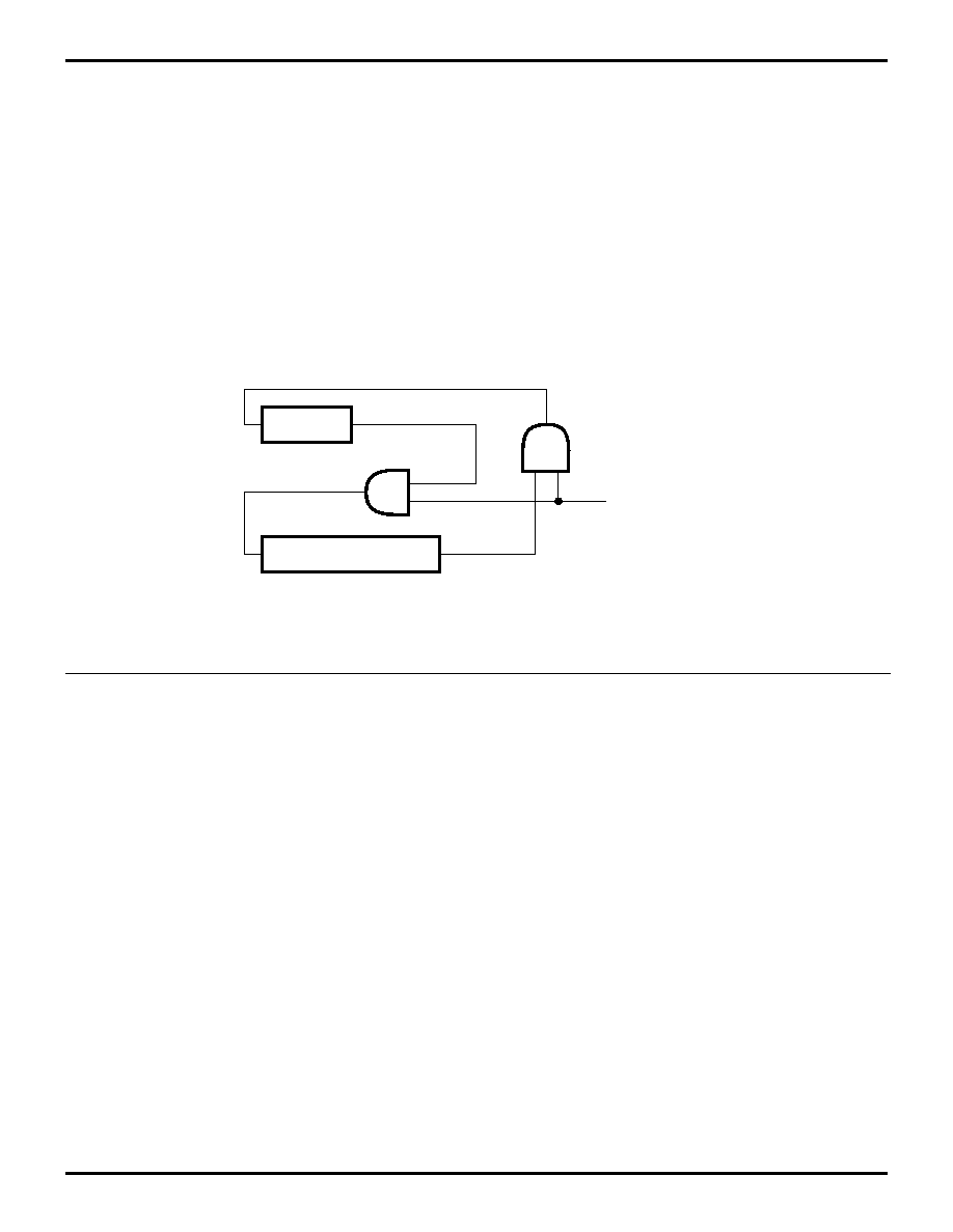
Figure 17. Glitch Filter Circuitry
Glitch
Filter
Edge
Detector
CTR1 D5,D4
CTR1 D3,D2
Pos Edge
Neg Edge
MUX
CTR1 D6
P31
P20
Figure 18. 8-Bit Counter/Timer Circuits
Z8 Data Bus
Pos Edge
Neg Edge
CTR0 D2
IRQ4
CTR0 D1
T8_OUT
TC8L
TC8H
Clock
Select
SCLK
CTR0 D4, D3
Clock
8-Bit
Counter T8
HI8
LO8
Z8 Data Bus
Z86L70/71/75/C71
IR/Low-Voltage Microcontroller
Zilog
1-30
P R E L I M I N A R Y
DS97LVO0500
FUNCTIONAL DESCRIPTION (Continued)
Input Circuit
The edge detector monitors the input signal on P31 or P20.
Based on CTR1 D5-D4, a pulse is generated at the Pos
Edge or Neg Edge line when an edge is detected. Glitches
in the input signal which have a width less than specified
(CTR1 D3, D2) are filtered out.
T8 Transmit Mode
When T8 is enabled, the output of T8 depends on CTR1,
D1. If it is 0, T8_OUT is 1. If it is 1, T8_OUT is 0.
When T8 is enabled, the output T8_OUT switches to the
initial value (CTR1 D1). If the initial value (CTR1 D1) is 0,
TC8L is loaded, otherwise TC8H is loaded into the
counter. In Single-Pass Mode (CTR0 D6), T8 counts down
to 0 and stops, T8_OUT toggles, the time-out status bit
(CTR0 D5) is set, and a time-out interrupt can be generat-
ed if it is enabled (CTR0 D1) (Figure 22). In Modulo-N
Mode, upon reaching terminal count, T8_OUT is toggled,
but no interrupt is generated. Then T8 loads a new count
(if the T8_OUT level now is 0), TC8L is loaded; if it is 1,
TC8H is loaded. T8 counts down to 0, toggles T8_OUT,
sets the time-out status bit (CTR0 D5) and generates an
interrupt if enabled (CTR0 D1) (Figure 23). This completes
one cycle. T8 then loads from TC8H or TC8L according to
the T8_OUT level, and repeats the cycle.
The user can modify the values in TC8H or TC8L at any
time. The new values take effect when they are loaded.
Care must be taken not to write these registers at the time
the values are to be loaded into the counter/timer, to en-
sure known operation. An initial count of 1 is not al-
lowed (a non-function will occur). An initial count of 0
will cause TC8 to count from 0 to %FF to %FE (Note, % is
used for hexadecimal values). Transition from 0 to %FF is
not a time-out condition.
Note: Using the same instructions for stopping the
counter/timers and setting the status bits is not rec-
ommended. Two successive commands, first stopping
the counter/timers, then resetting the status bits is neces-
sary. This is required because it takes one counter/timer
clock interval for the initiated event to actually occur.
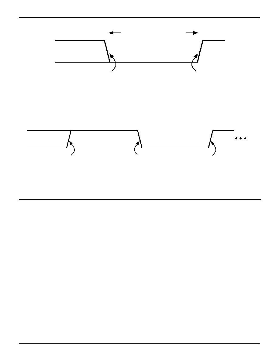
Figure 19. T8_OUT in Single-Pass Mode
TC8H Counts
"Counter Enable" Command,
T8_OUT Switches To Its
Initial Value (CTR1 D1)
T8_OUT Toggles,
Time-Out Interrupt
Figure 20. T8_OUT in Modulo-N Mode
"Counter Enable" Command,
T8_OUT Switches To Its
Initial Value (CTR1 D1)
T8_OUT Toggles
T8_OUT
TC8L
TC8H
TC8L
TC8H
TC8L
Time-Out Interrupt
Time-Out Interrupt
Z86L70/71/75/C71
Zilog
IR/Low-Voltage Microcontroller
DS97LVO0500
P R E L I M I N A R Y
1-31
1
T8 Demodulation Mode
The user should program TC8L and TC8H to %FF. After
T8 is enabled, when the first edge (rising, falling, or both
depending on CTR1 D5, D4) is detected, it starts to count
down. When a subsequent edge (rising, falling, or both de-
pending on CTR1 D5, D4) is detected during counting, the
current value of T8 is one's complemented and put into
one of the capture registers. If it is a positive edge, data is
put into LO8, if negative edge, HI8. One of the edge detect
status bits (CTR1 D1, D0) is set, and an interrupt can be
generated if enabled (CTR0 D2). Meanwhile, T8 is loaded
with %FF and starts counting again. Should T8 reach 0,
the time-out status bit (CTR0 D5) is set, an interrupt can be
generated if enabled (CTR0 D1), and T8 continues count-
ing from %FF (Figure 21).
Figure 21. Demodulation Mode Count Capture Flowchart
T8 (8-Bit)
Count Capture
T8_Enable
(Set By User)
No
Yes
Edge Present
No
Yes
What Kind Of Edge
Pos
T8
L08
Neg
T8
HI8
%FF
T8
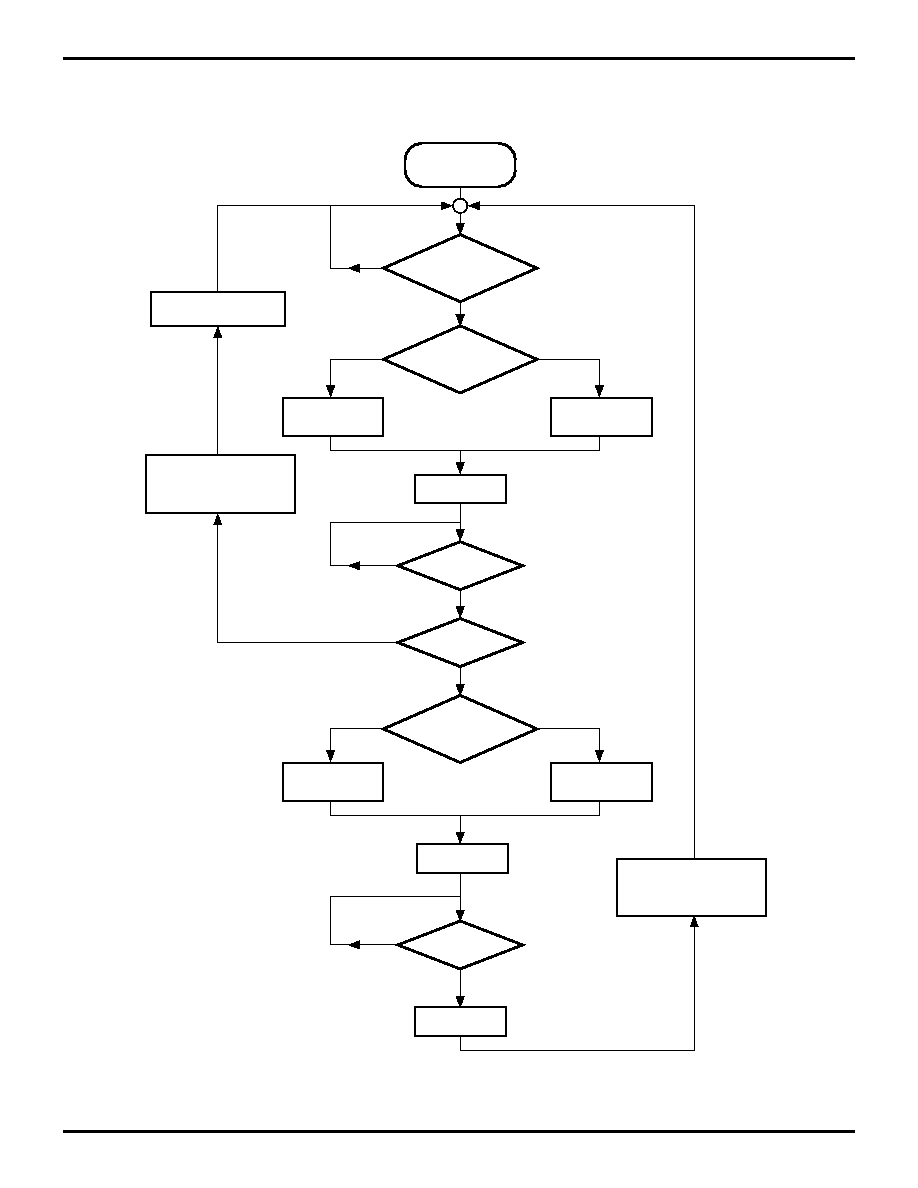
Z86L70/71/75/C71
IR/Low-Voltage Microcontroller
Zilog
1-32
P R E L I M I N A R Y
DS97LVO0500
FUNCTIONAL DESCRIPTION (Continued)
Figure 22. Transmit Mode Flowchart
T8 (8-Bit)
Transmit Mode
T8_Enable Bit Set
CTR0, D7
No
Yes
CTR1, D1
Value
1
Load TC8L
Reset T8_OUT
Load TC8H
Set T8_OUT
Enable T8
Reset T8_Enable Bit
Set Time-out Status Bit
(CTR0 D5) and Generate
Timeout_Int If Enabled
No
T8_Timeout
Yes
Single Pass?
Modulo-N
T8_OUT Value
Load TC8L
Reset T8_OUT
Load TC8H
Set T8_OUT
Enable T8
No
T8_Timeout
Disable T8
Yes
Set Time-out Status Bit
(CTR0 D5) and Generate
Timeout_Int If Enabled
Single Pass
0
1
0
Z86L70/71/75/C71
Zilog
IR/Low-Voltage Microcontroller
DS97LVO0500
P R E L I M I N A R Y
1-33
1
Figure 23. Demodulation Mode Flowchart
T8 (8-Bit)
Demodulation Mode
T8_Enable
CTR0, D7
No
Yes
Edge Present
No
T8_Enable Bit Set
Yes
Set Edge Present Status
Bit And Trigger Data
Capture Int. If Enabled
No
%FF
TC8
Yes
Enable TC8
Edge Present
Disable T8
Yes
T8 Time Out
Yes
Set Time-out Status
Bit And Trigger Time
Out Int. If Enabled
No
Continue Counting

Z86L70/71/75/C71
IR/Low-Voltage Microcontroller
Zilog
1-34
P R E L I M I N A R Y
DS97LVO0500
FUNCTIONAL DESCRIPTION (Continued)
T16 Transmit Mode
In Normal or Ping-Pong Mode, the output of T16 when not
enabled is dependent on CTR1, D0. If it is a 0, T16_OUT
is a 1; if it is a 1, T16_OUT is 0. The user can force the out-
put of T16 to either a 0 or 1 whether it is enabled or not by
programming CTR1 D3, D2 to a 10 or 11.
When T16 is enabled, TC16H * 256 + TC16L is loaded,
and T16_OUT is switched to its initial value (CTR1 D0).
When T16 counts down to 0, T16_OUT is toggled (in Nor-
mal or Ping-Pong Mode), an interrupt is generated if en-
abled (CTR2 D1), and a status bit (CTR2 D5) is set. Note
that global interrupts will override this function as de-
scribed in the interrupts section. If T16 is in Single-Pass
Mode, it is stopped at this point. If it is in Modulo-N Mode,
it is loaded with TC16H * 256 + TC16L and the counting
continues.
The user can modify the values in TC16H and TC16L at
any time. The new values take effect when they are load-
ed. Care must be taken not to load these registers at the
time the values are to be loaded into the counter/timer, to
ensure known operation. An initial count of 1 is not al-
lowed. An initial count of 0 will cause T16 to count from 0
to %FFFF to %FFFE. Transition from 0 to %FFFF is not a
time-out condition.
Figure 24. 16-Bit Counter/Timer Circuits
Z8 Data Bus
Pos Edge
Neg Edge
CTR2 D2
IRQ3
CTR2 D1
T16_OUT
TC16L
TC16H
Clock
Select
SCLK
CTR2 D4, D3
Clock
16-Bit
Counter
T16
HI16
LO16
Z8 Data Bus
Z86L70/71/75/C71
Zilog
IR/Low-Voltage Microcontroller
DS97LVO0500
P R E L I M I N A R Y
1-35
1
T16 Demodulation Mode
The user should program TC16L and TC16H to %FF. After
T16 is enabled, when the first edge (rising, falling, or both
depending on CTR1 D5, D4) is detected, T16 captures
HI16 and LO16 reloads and begins counting.
If D6 of CTR2 is 0: When a subsequent edge (rising, fall-
ing, or both depending on CTR1 D5, D4) is detected during
counting, the current count in T16 is one's complemented
and put into HI16 and LO16. When data is captured, one
of the edge detect status bits (CTR1 D1, D0) is set and an
interrupt is generated if enabled (CTR2 D2). T16 is loaded
with %FFFF and starts again.
If D6 of CTR2 is 1: T16 ignores the subsequent edges in
the input signal and continues counting down. A time out
of T8 will cause T16 to capture its current value and gen-
erate an interrupt if enabled (CTR2, D2). In this case, T16
does not reload and continues counting. If D6 bit of CTR2
is toggled (by writing a 0 then a 1 to it), T16 will capture and
reload on the next edge (rising, falling, or both depending
on CTR1 D5, D4) but continue to ignore subsequent edg-
es.
Should T16 reach 0, it continues counting from %FFFF;
meanwhile, a status bit (CTR2 D5) is set and an interrupt
time-out can be generated if enabled (CTR2 D1).
Figure 25. T16_OUT in Single-Pass Mode
TC16H*256+TC16L Counts
"Counter Enable" Command,
T16_OUT Switches To Its
Initial Value (CTR1 D0)
T16_OUT Toggles,
Time-Out Interrupt
Figure 26. T16_OUT in Modulo-N Mode
TC16H*256+TC16L
"Counter Enable" Command,
T16_OUT Switches To Its
Initial Value (CTR1 D0)
T16_OUT Toggles,
Time-Out Interrupt
TC16H*256+TC16L
TC16H*256+TC16L
T16_OUT Toggles,
Time-Out Interrupt
T16_OUT
Z86L70/71/75/C71
IR/Low-Voltage Microcontroller
Zilog
1-36
P R E L I M I N A R Y
DS97LVO0500
FUNCTIONAL DESCRIPTION (Continued)
Ping-Pong Mode
This operation mode is only valid in Transmit Mode. T8
and T16 need to be programmed in Single-Pass Mode
(CTR0 D6, CTR2 D6) and Ping-Pong Mode needs to be
programmed in CTR1 D3, D2. The user can begin the op-
eration by enabling either T8 or T16 (CTR0 D1 or CTR2
D7). For example, if T8 is enabled, T8_OUT is set to this
initial value (CTR1 D1). According to T8_OUT's level,
TC8H or TC8L is loaded into T8. After the terminal count
is reached, T8 is disabled and T16 is enabled. T16_OUT
switches to its initial value (CTR1 D0), data from TC16H
and TC16L is loaded, and T16 starts to count. After T16
reaches the terminal count it stops, T8 is enabled again,
and the whole cycle repeats. Interrupts can be allowed
when T8 or T16 reaches terminal control (CTR0 D1, CTR2
D1). To stop the Ping-Pong operation, write 00 to bits D3
and D2 of CTR1.
Note:Enabling Ping-Pong operation while the
counter/timers are running may cause intermittent
counter/timer function. Disable the counter/timers, then
reset the status flags prior to instituting this operation.
To Initiate Ping-Pong Mode
First, make sure both counter/timers are not running. Then
set T8 into Single-Pass Mode (CTR0 D6), set T16 into Sin-
gle-Pass Mode (CTR2 D6), and set Ping-Pong Mode
(CTR1 D2, D3). These instructions do not have to be in
any particular order. Finally, start Ping-Pong Mode by en-
abling either T8 (CTR0 D7) or T16 (CTR2 D7).
During Ping-Pong Mode
The enable bits of T8 and T16 (CTR0 D7, CTR2 D7) will
be alternately set and cleared by hardware. The time-out
bits (CTR0 D5, CTR2 D5) will be set every time the
counter/timers reach the terminal count.
Figure 27. Ping-Pong Mode
Enable
TC8
Time-Out
Enable
TC16
Time-Out
Ping-Pong
CTR1 D3,D2
Z86L70/71/75/C71
Zilog
IR/Low-Voltage Microcontroller
DS97LVO0500
P R E L I M I N A R Y
1-37
1
To Terminate Ping-Pong Mode
Change Transmit Mode to Normal Mode (CTR1 D2, D3).
Notice that Ping-Pong Mode is not actually stopped until
one of the timer/counter's time-out. Before the actual ter-
mination of Ping-Pong Mode, the user should not change
the value of CTR0 or CTR2, except for resetting the time-
out status bit. Here is an example for terminating Ping-
Pong Mode safely:
or
CTR0,#%20
;reset T8 time-out status bit
loop_a:
tm
CTR0,#%20
jr
z,loop_a
;wait until T8 times-out
Id
CTR1,#00000000b
;change to Normal Mode
or
CTR2,#%20
;reset T16 time-out status bit
loop_b:
tm
CTR2,#%20
jr
z,loop_b
;wait until T16 times-out
;now Ping-Pong Mode is actually
Id
CTR0,#00100000b
;terminated and user can re-program T8
Id
CTR2,#00100000b
;and T16
Figure 28. T8_OUT and T16_OUT in Ping-Pong Mode
TC8H
Enable T8,
T8_OUT Switches
To Its Initial Value
TC16H*256+TC16L
T16_OUT Toggles
T8_OUT
TC8H
TC16H*256+TC16L
T16_OUT
T16_OUT
T16_OUT Switches To Its Initial
Value When TC16 Is Enabled
T8_OUT Toggles
T8_OUT Toggles
Z86L70/71/75/C71
IR/Low-Voltage Microcontroller
Zilog
1-38
P R E L I M I N A R Y
DS97LVO0500
FUNCTIONAL DESCRIPTION (Continued)
Figure 29. Output Circuit
AND/OR/NOR/NAND
Logic
T8_OUT
CTR1 D5,D4
P34_INTERNAL
CTR0 D0
P36_INTERNAL
CTR1 D6
P35_INTERNAL
CTR2 D0
P35_EXT
P36_EXT
P34_EXT
MUX
MUX
MUX
T16_OUT
MUX
CTR1, D2
CTR1 D3
Z86L70/71/75/C71
Zilog
IR/Low-Voltage Microcontroller
DS97LVO0500
P R E L I M I N A R Y
1-39
1
Interrupts. The Z86L7X has five different interrupts. The
interrupts are maskable and prioritized (Figure 30). The
five sources are divided as follows: three sources are
claimed by Port 3 lines P33-P31, the remaining two by the
counter/timers (Table 3). The Interrupt Mask Register glo-
bally or individually enables or disables the five interrupt
requests.
Figure 30. Interrupt Block Diagram
Interrupt
Edge
Select
IRQ Register (D6, D7)
IRQ 1, 3, 4
IRQ
IMR
IPR
Priority
Logic
5
Vector Select
IRQ0
IRQ2
Global
Interrupt
Enable
Interrupt
Request
Z86L70/71/75/C71
IR/Low-Voltage Microcontroller
Zilog
1-40
P R E L I M I N A R Y
DS97LVO0500
FUNCTIONAL DESCRIPTION (Continued)
When more than one interrupt is pending, priorities are re-
solved by a programmable priority encoder controlled by
the Interrupt Priority register. An interrupt machine cycle is
activated when an interrupt request is granted. This dis-
ables all subsequent interrupts, saves the Program
Counter and Status Flags, and then branches to the pro-
gram memory vector location reserved for that interrupt.
All Z86L7X interrupts are vectored through locations in the
program memory. This memory location and the next byte
contain the 16-bit address of the interrupt service routine
for that particular interrupt request. To accommodate
polled interrupt systems, interrupt inputs are masked and
the Interrupt Request register is polled to determine which
of the interrupt requests need service.
An interrupt resulting from AN1 (P31) is mapped into IRQ2,
and an interrupt from AN2 (P32) is mapped into IRQ0. In-
terrupts IRQ2 and IRQ0 may be rising, falling, or both edge
triggered, and are programmable by the user. The soft-
ware can poll to identify the state of the pin.
Programming bits for the Interrupt Edge Select are located
in the IRQ Register (R250), bits D7 and D6 . The configu-
ration is shown in Table 4.
Clock. The Z86L7X on-chip oscillator has a high-gain, par-
allel-resonant amplifier for connection to a crystal, LC, ce-
ramic resonator, or any suitable external clock source
(XTAL1 = Input, XTAL2 = Output). The crystal should be
AT cut, 1 MHz to 8 MHz maximum, with a series resistance
(RS) less than or equal to 100 Ohms. The Z86L7X on-chip
oscillator may be driven with a cost-effective RC network
or other suitable external clock source.
The crystal should be connected across XTAL1 and
XTAL2 using the recommended capacitors (capacitance
greater than or equal to 22 pF) from each pin to ground.
The RC oscillator configuration is an external resistor con-
nected from XTAL1 to XTAL2, with a frequency-setting ca-
pacitor from XTAL1 to ground (Figure 8).
Table 3. Interrupt Types, Sources, and Vectors
Name
Source
Vector
Location
Comments
IRQ0
/DAV0, IRQ0
0, 1
External (P32),
Rising Falling Edge
Triggered
IRQ1,
IRQ1
2, 3
External (P33),
Falling Edge
Triggered
IRQ2
/DAV2, IRQ2,
T
IN
4, 5
External (P31),
Rising Falling Edge
Triggered
IRQ3
T16
6, 7
Internal
IRQ4
T8
8, 9
Internal
Table 4. IRQ Register
IRQ
Interrupt Edge
D7
D6
IRQ2 (P31)
IRQ0 (P32)
0
0
F
F
0
1
F
R
1
0
R
F
1
1
R/F
R/F
Notes:
F = Falling Edge
R = Rising Edge
In analog mode, the Stop-Mode Recovery sources selected by
the SMR register are connected to the IRQ1 input. Any of the
Stop-Mode Recovery sources for SMR (except P31, P32, and
P33) can be used to generate IRQ1 (falling edge triggered)
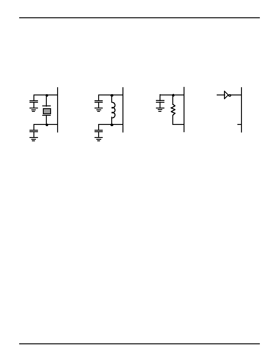
Z86L70/71/75/C71
Zilog
IR/Low-Voltage Microcontroller
DS97LVO0500
P R E L I M I N A R Y
1-41
1
Power-On Reset (POR). A timer circuit clocked by a ded-
icated on-board RC oscillator is used for the Power-On Re-
set (POR) timer function. The POR time allows V
CC
and
the oscillator circuit to stabilize before instruction execu-
tion begins.
The POR timer circuit is a one-shot timer triggered by one
of three conditions:
1.
Power Fail to Power OK status.
2.
Stop-Mode Recovery (if D5 of SMR = 1).
3.
WDT Time-Out.
The POR time is a nominal 5 ms. Bit 5 of the Stop-Mode
Register determines whether the POR timer is bypassed
after Stop-Mode Recovery (typical for external clock, RC,
LC oscillators).
Figure 31. Oscillator Configuration
XTAL1
XTAL2
C1
C2
C1
C2
C1
XTAL1
XTAL2
XTAL1
XTAL2
XTAL1
XTAL2
Ceramic Resonator or Crystal
C1, C2 = 47 pF TYP *
f = 8 MHz
LC
C1, C2 = 22 pF
L = 130
µ
H *
f = 3 MHz *
RC
@ 3V VCC (TYP)
C1 = 33 pF *
R = 1K *
External Clock
L
R
* Preliminary value including pin parasitics
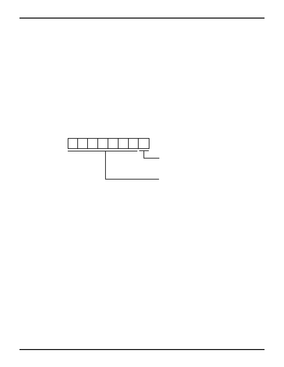
Z86L70/71/75/C71
IR/Low-Voltage Microcontroller
Zilog
1-42
P R E L I M I N A R Y
DS97LVO0500
FUNCTIONAL DESCRIPTION (Continued)
HALT. HALT turns off the internal CPU clock, but not the
XTAL oscillation. The counter/timers and external inter-
rupts IRQ0, IRQ1, IRQ2, IRQ3, and IRQ4 remain active.
The devices are recovered by interrupts, either externally
or internally generated. An interrupt request must be exe-
cuted (enabled) to exit HALT Mode. After the interrupt ser-
vice routine, the program continues from the instruction af-
ter the HALT.
STOP. This instruction turns off the internal clock and ex-
ternal crystal oscillation and reduces the standby current
to 10
µ
A or less. STOP Mode is terminated only by a reset,
such as WDT time-out, POR, SMR, or external reset. This
causes the processor to restart the application program at
address 000CH. In order to enter STOP (or HALT) mode,
it is necessary to first flush the instruction pipeline to avoid
suspending execution in mid-instruction. To do this, the
user must execute a NOP (opcode = FFH) immediately be-
fore the appropriate sleep instruction, i.e.,
FF
NOP
; clear the pipeline
6F
STOP
; enter STOP Mode
or
FF
NOP
; clear the pipeline
7F
HALT
; enter HALT Mode
Port Configuration Register (PCON). The PCON regis-
ter configures the comparator output on Port 3. It is locat-
ed in the expanded register file at Bank F, location 00 (Fig-
ure 32).
Figure 32. Port Configuration Register (PCON)
(Write Only)
Reserved (Must be 1)
D7
D6
D5
D4 D3
D2
D1
D0
PCON (FH) 00H
Comparator Output Port 3
0 P34,Standard Output*
1 P34,Comparator Output
* Default Setting After Reset
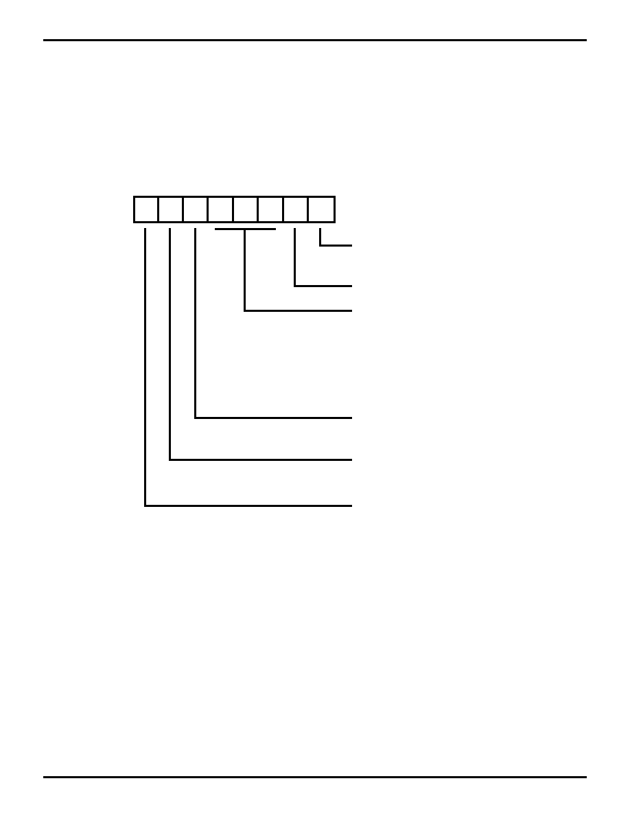
Z86L70/71/75/C71
Zilog
IR/Low-Voltage Microcontroller
DS97LVO0500
P R E L I M I N A R Y
1-43
1
Comparator Output Port 3 (D0). Bit 0 controls the com-
parator used in Port 3. A 1 in this location brings the com-
parator outputs to P34 and P37, and a 0 releases the Port
to its standard I/O configuration.
Stop-Mode Recovery Register (SMR). This register se-
lects the clock divide value and determines the mode of
Stop-Mode Recovery (Figure 33). All bits are write only ex-
cept bit 7, which is read only. Bit 7 is a flag bit that is hard-
ware set on the condition of STOP recovery and reset by
a power-on cycle. Bits D2, D3, and D4, of the SMR regis-
ter, specify the source of the Stop-Mode Recovery signal.
Bit D0 determines if SCLK/TCLK are divided by 16 or not.
The SMR is located in Bank F of the Expanded Register
Group at address 0BH.
Figure 33. Stop-Mode Recovery Register
D7
D6
D5
D4
D3
D2
D1
D0
SMR (0F) 0B
SCLK/TCLK Divide-by-16
0 OFF
1 ON
Reserved (Must be 0)
Stop-Mode Recovery Source
000
001
010
0 11
100
101
11 0
111
Stop Delay
0 OFF
1 ON
Reserved
0 Low
Reserved Must be 0
Stop Flag
0 POR
1 Stop Recovery * *
* Default Setting After Reset
** Default Setting After Reset and Stop-Mode Recovery
**
*
*
*
*
POR Only
Reserved
P31
P32
P33
P27
P2 NOR 0-3
P2 NOR 0-7
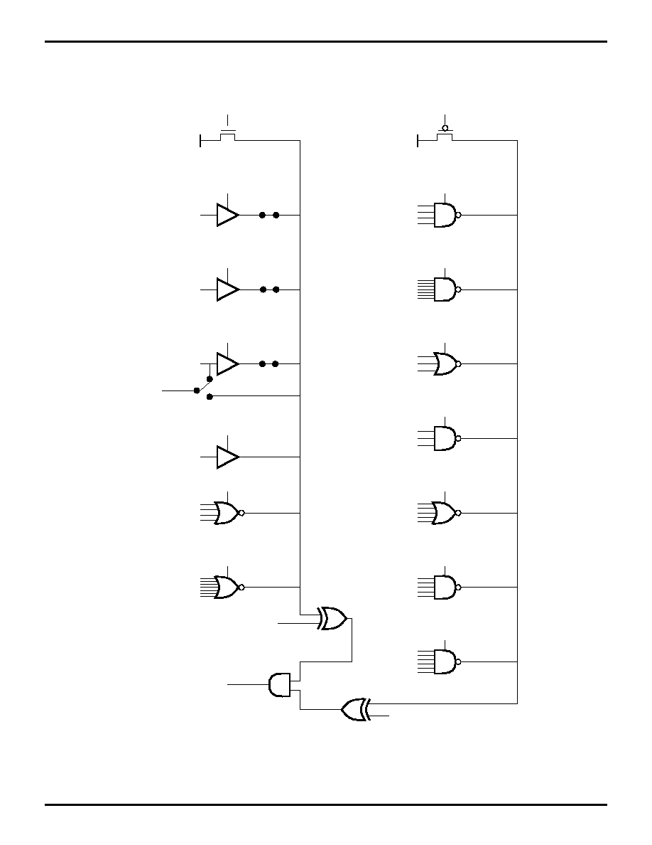
Z86L70/71/75/C71
IR/Low-Voltage Microcontroller
Zilog
1-44
P R E L I M I N A R Y
DS97LVO0500
FUNCTIONAL DESCRIPTION (Continued)
Figure 34. Stop-Mode Recovery Source
P00
P32
VCC
P31
P32
P33
P27
P20
P23
P20
P27
SMR D4
0
D3
0
D2
0
SMR D4
0
D3
1
D2
0
SMR D4
0
D3
1
D2
1
SMR D4
1
D3
0
D2
0
SMR D4
1
D3
0
D2
1
SMR D4
1
D3
1
D2
0
SMR D4
1
D3
1
D2
1
SMR2 D4
0
D3
0
D2
0
SMR2 D4
0
D3
1
D2
0
SMR2 D4
0
D3
1
D2
1
SMR2 D4
1
D3
0
D2
0
SMR2 D4
1
D3
0
D2
1
SMR2 D4
1
D3
1
D2
0
SMR2 D4
1
D3
1
D2
1
SMR2 D4
0
D3
0
D2
1
VCC
P20
P32
P23
P20
P27
P31
P33
P31
P33
P32
P31
P33
P00
P07
P32
P31
P33
P07
P20
P32
P31
P33
P21
P22
SMR2 D6
SMR D6
To RESET and WDT
Circuitry (Active Low)
S1
S2
S3
S4
To IRQ1
(= 0)
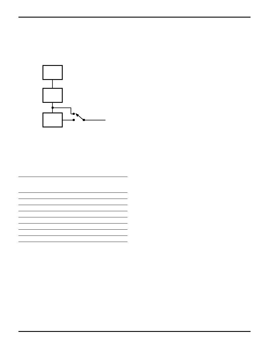
Z86L70/71/75/C71
Zilog
IR/Low-Voltage Microcontroller
DS97LVO0500
P R E L I M I N A R Y
1-45
1
SCLK/TCLK Divide-by-16 Select (D0). D0 of the SMR
controls a Divide-by-16 prescaler of SCLK/TCLK. The pur-
pose of this control is to selectively reduce device power
consumption during normal processor execution (SCLK
control) and/or HALT Mode (where TCLK sources interrupt
logic). After Stop-Mode Recovery, this bit is set to a 0.
Stop-Mode Recovery Source (D2, D3, and D4). These
three bits of the SMR specify the wake up source of the
STOP recovery (Figure 36 and Table 5).
P33-P31 cannot wake up from STOP Mode if the input
lines are configured as analog input.
Note: Port pins defined as an output will drive the corre-
sponding input to the default state to allow the remaining
inputs to control the AND/OR function. Refer to SMR2 reg-
ister for other recover sources.
Stop-Mode Recovery Delay Select (D5). This bit, if Low,
disables the 5 ms /RESET delay after Stop-Mode Recov-
ery. The default configuration of this bit is one. If the "fast"
wake up is selected, the Stop-Mode Recovery source
needs to be kept active for at least 5TpC.
Stop-Mode Recovery Edge Select (D6). A 1 in this bit po-
sition indicates that a High level on any one of the recovery
sources wakes the Z86L7X from STOP Mode. A 0 indi-
cates Low level recovery. The default is 0 on POR (Figure
36).
Cold or Warm Start (D7). This bit is set by the device
upon entering STOP Mode. It is a Read Only Flag bit. A 1
in D7 (warm) indicates that the device will awaken from a
SMR source or a WDT while in STOP Mode. A 0 in this bit
(cold) indicates that the device will be reset by a POR,
WDT while not in STOP, or the device awakened a low
voltage standby mode.
Stop-Mode Recovery Register 2 (SMR). This register
determines the mode of the Stop-Mode Recovery for
SMR2.
If SMR2 is used in conjunction with SMR, either of the
specified events will cause a Stop-Mode Recovery.
Figure 35. SCLK Circuit
Table 5. Stop-Mode Recovery Source
SMR:432
Operation
D4
D3
D2
Description of Action
0
0
0
POR and/or external reset recovery
0
0
1
Reserved
0
1
0
P31 transition
0
1
1
P32 transition
1
0
0
P33 transition
1
0
1
P27 transition
1
1
0
Logical NOR of P20 through P23
1
1
1
Logical NOR of P20 through P27
SMR, D0
˜
2
˜
16
OSC
SCLK
TCLK
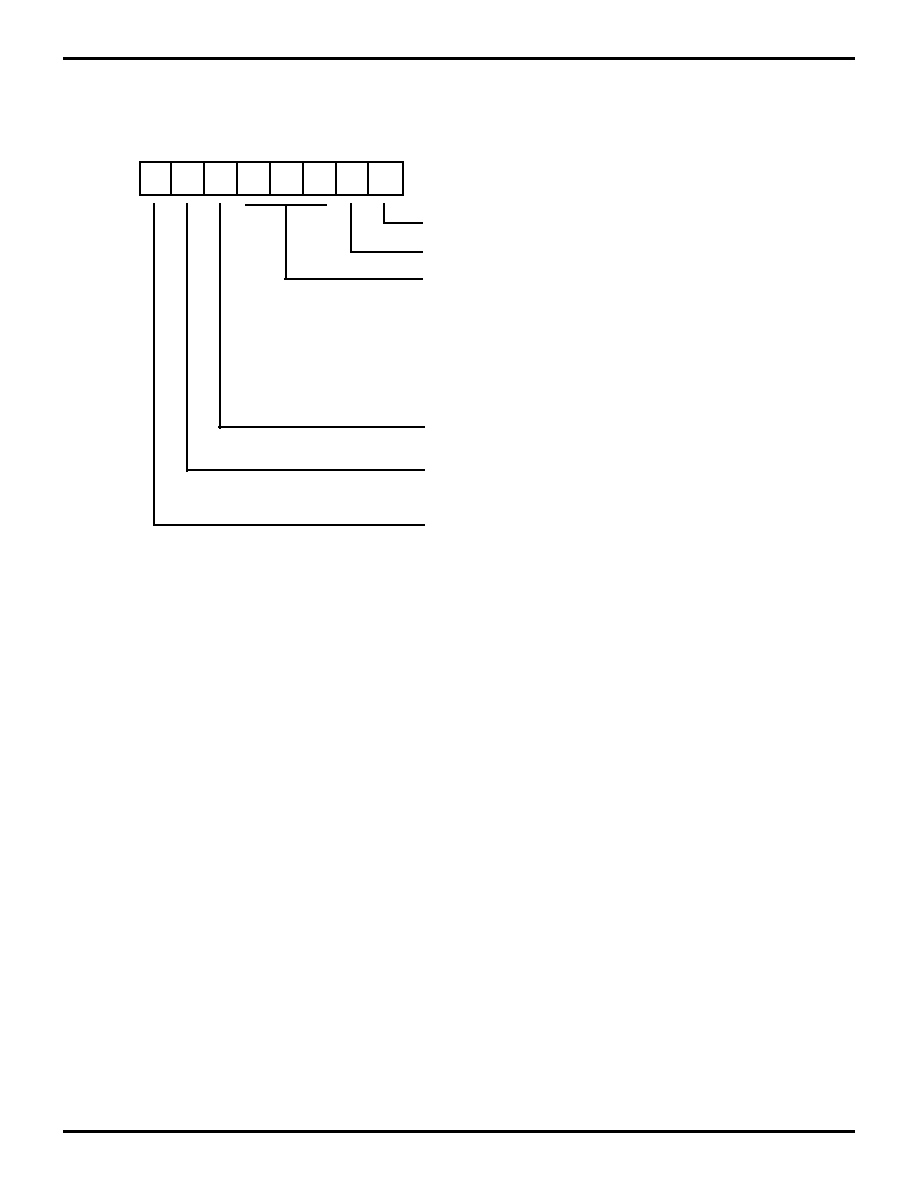
Z86L70/71/75/C71
IR/Low-Voltage Microcontroller
Zilog
1-46
P R E L I M I N A R Y
DS97LVO0500
FUNCTIONAL DESCRIPTION (Continued)
Figure 36. Stop-Mode Recovery Register 2
((0F) 0DH: D2-D4: D6 Write Only)
D7 D6
D5
D4
D3
D2
D1
D0
SMR2 (0F) 0DH
Reserved (Must be 0)
Reserved (Must be 0)
Stop-Mode Recovery Source 2
000 POR only*
001 NAND P20, P21, P22, P23
010 NAND P20, P21, P22, P23, P24, P25, P26, P27
011 NOR P31, P32, P33
100 NAND P31, P32, P33
101 NOR P31, P32, P33, P00, P07
110 NAND P31, P32, P33, P00, P07
111 NAND P31, P32, P33, P20, P21, P22
Reserved
(Must be 0)
Recovery Level
0 Low*
1 High
Reserved (Must be 0)
Note: If used in conjunction with SMR,
either of the two specified events will
cause a Stop-Mode Recovery.
*Default Setting After Reset
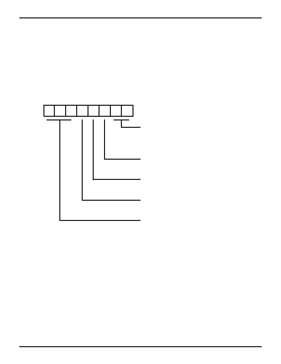
Z86L70/71/75/C71
Zilog
IR/Low-Voltage Microcontroller
DS97LVO0500
P R E L I M I N A R Y
1-47
1
Watch-Dog Timer Mode Register (WDTMR). The WDT
is a retriggerable one-shot timer that resets the Z8 if it
reaches its terminal count. The WDT must initially be en-
abled by executing the WDT instruction and refreshed on
subsequent executions of the WDT instruction. The WDT
circuit is driven by an on-board RC oscillator or external
oscillator from the XTAL1 pin. The WDT instruction affects
the Zero (Z), Sign (S), and Overflow (V) flags.
The POR clock source is selected with bit 4 of the WDT
register. Bit 0 and 1 control a tap circuit that determines the
time-out period. Bit 2 determines whether the WDT is ac-
tive during HALT and Bit 3 determines WDT activity during
STOP. Bits 5 through 7 are reserved (Figure 37). This reg-
ister is accessible only during the first 64 processor cycles
(128 XTAL clocks) from the execution of the first instruc-
tion after Power-On-Reset, Watch-Dog Reset, or a Stop-
Mode Recovery (Figure 40). After this point, the register
cannot be modified by any means, intentional or other-
wise. The WDTMR cannot be read and is located in Bank
F of the Expanded Register Group at address location
0FH. It is organized as follows:
Figure 37. Watch-Dog Timer Mode Register
(Write Only)
D7
D6
D5
D4
D3
D2
D1
D0
WDTMR (0F) 0F
WDT TAP INT RC OSC External Clock
00 5 ms 256 TpC
01 10 ms 512 TpC
10 20 ms 1024 TpC
11 80 ms 4096 TpC
WDT During HALT
0 OFF
1 ON
WDT During STOP
0 OFF
1 ON
XTAL1/INT RC Select for WDT
0 On-Chip RC
1 XTAL
Reserved (Must be 0)
* Default Setting After Reset
*
*
*
*
Z86L70/71/75/C71
IR/Low-Voltage Microcontroller
Zilog
1-48
P R E L I M I N A R Y
DS97LVO0500
FUNCTIONAL DESCRIPTION (Continued)
WDT Time Select (D0, D1). Selects the WDT time period.
It is configured as shown in Table 6.
WDTMR During HALT (D2). This bit determines whether
or not the WDT is active during HALT Mode. A 1 indicates
active during HALT. The default is 1.
WDTMR During STOP (D3). This bit determines whether
or not the WDT is active during STOP Mode. Since the
XTAL clock is stopped during STOP Mode, the on-board
RC has to be selected as the clock source to the
WDT/POR counter. A 1 indicates active during STOP. The
default is 1.
Clock Source for WDT (D4). This bit determines which
oscillator source is used to clock the internal POR and
WDT counter chain. If the bit is a 1, the internal RC oscil-
lator is bypassed and the POR and WDT clock source is
driven from the external pin, XTAL1. The default configu-
ration of this bit is 0, which selects the RC oscillator.
Table 6. WDT Time Select
D1
D0
Time-Out of
Internal RC OSC
Time-Out of
XTAL Clock
0
0
5 ms min
256 TpC
0
1
10 ms min
512 TpC
1
0
20 ms min
1024 TpC
1
1
80 ms min
4096 TpC
Notes:
1. TpC = XTAL clock cycle.
2. The default on reset is 10 ms.
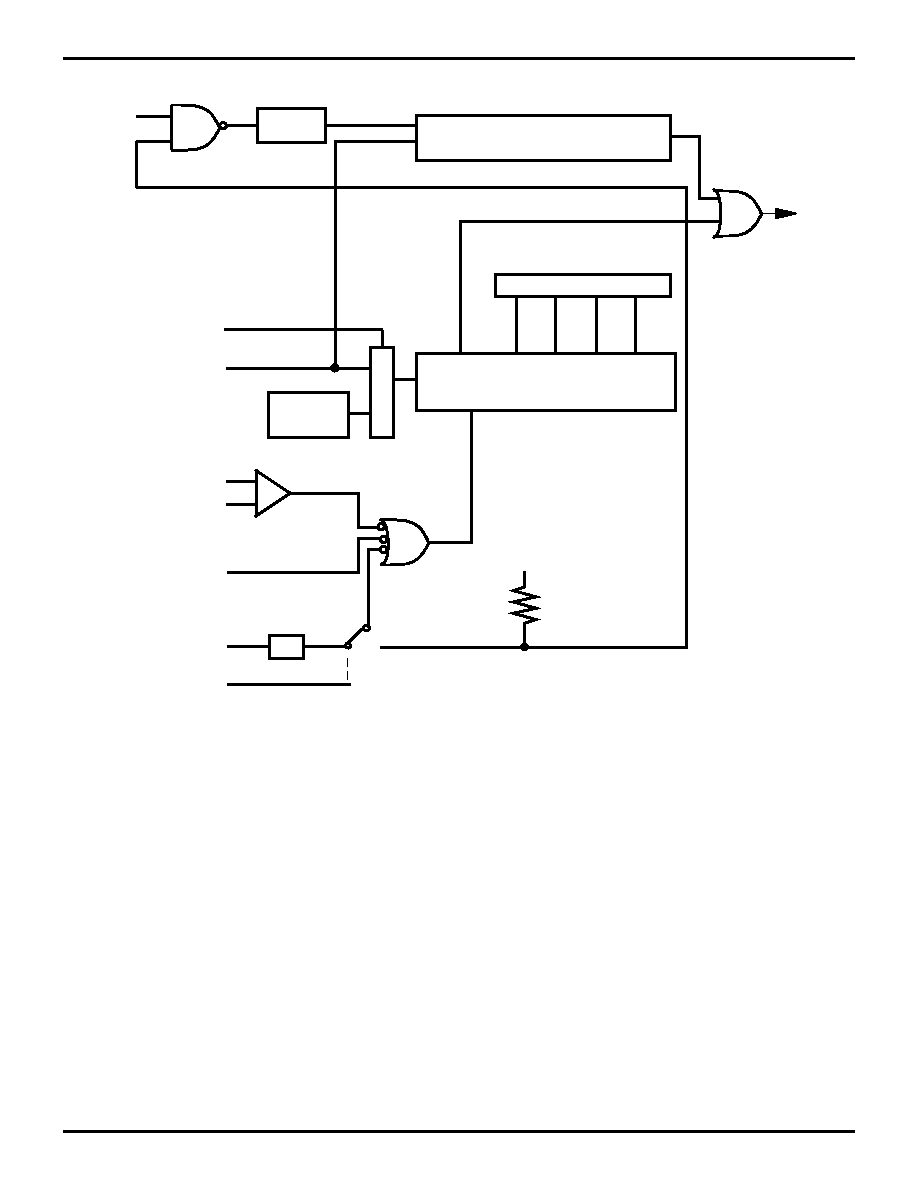
Z86L70/71/75/C71
Zilog
IR/Low-Voltage Microcontroller
DS97LVO0500
P R E L I M I N A R Y
1-49
1
Figure 38. Resets and WDT
CLK
18 Clock RESET
Generator
RESET
* /CLR 2
WDT TAP SELECT
INTERNAL
RC
OSC.
CLK
*/CLR1
POR
WDT1
2
3
4
Low Operating
Voltage Det.
Internal
RESET
Active
High
CK Source
Select
(WDTMR)
XTAL
VDD
VBO/VLV
2V REF.
From Stop
Mode
Recovery
Source
WDT
Stop Delay
Select (SMR)
12 ns Glitch Filter
+
-
5 Clock
Filter
WDT/POR Counter Chain
M
U
X
/RESET
* /CLR1 and /CLR2 enable the WDT/POR and
18 Clock Reset timers upon a Low to High input transition.
VCC
Z86L70/71/75/C71
IR/Low-Voltage Microcontroller
Zilog
1-50
P R E L I M I N A R Y
DS97LVO0500
FUNCTIONAL DESCRIPTION (Continued)
Low Voltage Detection/Protection. An on-chip Voltage
Comparator checks that the V
CC
is at the required level for
correct operation of the device. Reset is globally driven
when V
CC
falls below V
LV
(Vrf1).
Mask Selectable Options. There are six Mask Selectable
Options to choose from based on ROM code require-
ments.
Note: Internal Port 0/Pull-Up resistors remain connected
when port pins are configured as outputs.
The Low Voltage trip voltage (V
LV
) is less than 2.1V under
the following conditions:
Maximum (V
LV
) Conditions:
T
A
= 0
∞
C, +55
∞
C Internal clock frequency equal to or less
than 4.0 MHz
Note: The internal clock frequency is one-half the external
clock frequency.
The device is guaranteed to function normally until the Low
Voltage Protection trip point V
LV
is reached, below which
reset is globally driven. The device is guaranteed to func-
tion normally at supply voltages above the V
LV
trip point for
the temperatures and operating frequencies in maximum
V
LV
conditions. The actual V
LV
trip point is a function of
temperature and process parameters (Figure 39).
Permanent Watch-Dog
Timer
On/WDT command invoked
RAM Protect
On/Off
ROM Protect
On/Off
32 kHz XTAL
On/Off
Port 00-07 Pull-ups
On/Off
Port 31-33 Pull-ups
On/Off
Port 20-27 Pull-ups
On/Off
Figure 39. Typical Z86L7X Low Voltage vs
Temperature at 8 MHz
0
15
25
35
45
55
1.8
1.6
1.4
1.2
1
0.8
0.6
0.4
0.2
0
VL
V
VLV
Temperature
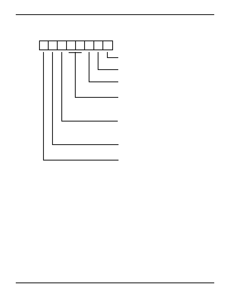
Z86L70/71/75/C71
Zilog
IR/Low-Voltage Microcontroller
DS97LVO0500
P R E L I M I N A R Y
1-51
1
EXPANDED REGISTER FILE CONTROL REGISTERS (0D)
Figure 40. TC8 Control Register
((0D) 0H: Read/Write Except Where Noted)
D7
D6
D5
D4
D3
D2
D1
D0
CTR0 (0D) 0H
0 P34 as Port Output
1 Timer8 Output
0 Disable T8 Time Out Interrupt
1 Enable T8 Time Out Interrupt
0 Disable T8 Data Capture Interrupt
1 Enable T8 Data Capture Interrupt
00 SCLK on T8
01 SCLK/2 on T8
10 SCLK/4 on T8
11 SCLK/8 on T8
R 0 No T8 Counter Time Out
R 1 T8 Counter Time Out Occured
W 0 No Effect
W 1 Reset Flag to 0
* Default Setting After Reset
0 Modulo-N
1 Single Pass
R 0 T8 Disabled *
R 1 T8 Enabled
W 0 Stop T8
W 1 Enable T8
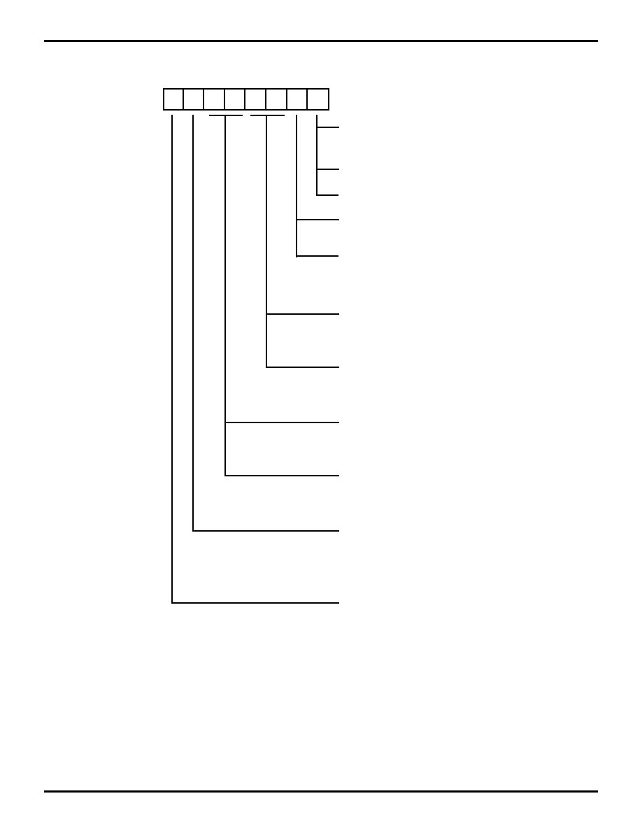
Z86L70/71/75/C71
IR/Low-Voltage Microcontroller
Zilog
1-52
P R E L I M I N A R Y
DS97LVO0500
Figure 41. T8 and T16 Common Control Functions
((0D) 1H: Read/Write)
D7
D6
D5
D4
D3
D2
D1
D0
CTR1 (0D) 1H
0 T16_OUT is 0 Initially
1 T16_OUT is 1 Initially
R/W
R
R
W
W
0 No Falling Edge Detection
1 Falling Edge Detection
0 No Effect
1 Reset Flag to 0
0 T8_OUT is 0 Initially
1 T8_OUT is 1 Initially
0 No Rising Edge Detection
1 Rising Edge Detection
0 0 Normal Operation
0 1 Ping-Pong Mode
1 0 T16_OUT = 0
1 1 T16_OUT = 1
Transmit Mode/T8/T16 Logic
0 0 Falling Edge Detection
0 1 Rising Edge Detection
1 0 Both Edge Detection
1 1 Reserved
0 P36 as Port Output *
1 P36 as T8/T16_OUT
0 Transmit Mode *
1 Demodulation Mode
0 0 No Filter
0 1 4 SCLK Cycle Filter
1 0 8 SCLK Cycle Filter
1 1 16 SCLK Cycle Filter
Demodulation Mode
Transmit Mode
Transmit Mode
R/W
Demodulation Mode
R
R
W
W
Transmit Mode
Demodulation Mode
0 0 AND
0 1 OR
1 0 NOR
1 1 NAND
Demodulation Mode
Transmit Mode
0 P31 as Demodulator Input
1 P20 as Demodulator Input
Demodulation Mode
Transmit/Demodulation Modes
0 No Effect
1 Reset Flag to 0
Note: Care must be taken in differentiating
Transmit Mode from Demodulation Mode.
Depending on which of these two modes is
operating, the CTR1 bit will have different
functions.
*Note: Changing from one mode to
another cannot be done without
disabling the counter/timers.
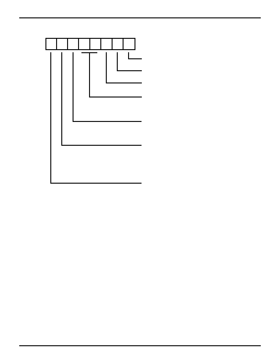
Z86L70/71/75/C71
Zilog
IR/Low-Voltage Microcontroller
DS97LVO0500
P R E L I M I N A R Y
1-53
1
Figure 42. T16 Control Register
((0D) 2H: Read/Write Except Where Noted)
D7 D6
D5
D4
D3
D2
D1
D0
CTR2 (0D) 02H
0 P35 is Port Output
1 P35 is TC16 Output
0 Disable T16 Time-Out Interrupt
1 Enable T16 Time-Out Interrupt
0 0 SCLK on T16
0 1 SCLK/2 on T16
1 0 SCLK/4 on T16
1 1 SCLK/8 on T16
* Default Setting After Reset
0 Disable T16 Data Capture Interrupt
1 Enable T16 Data Capture Interrupt
R 0 No T16 Time Out
R 1 T16 Time Out Occurs
W 0 No Effect
W 1 Reset Flag to 0
0 Modulo-N for T16
1 Single Pass for T16
R 0 T16 Disabled *
R 1 T16 Enabled
W 0 Stop T16
W 1 Enable T16
Transmit Mode
0 T16 Recognizes Edge
1 T16 Does Not Recognize Edge
Demodulator Mode
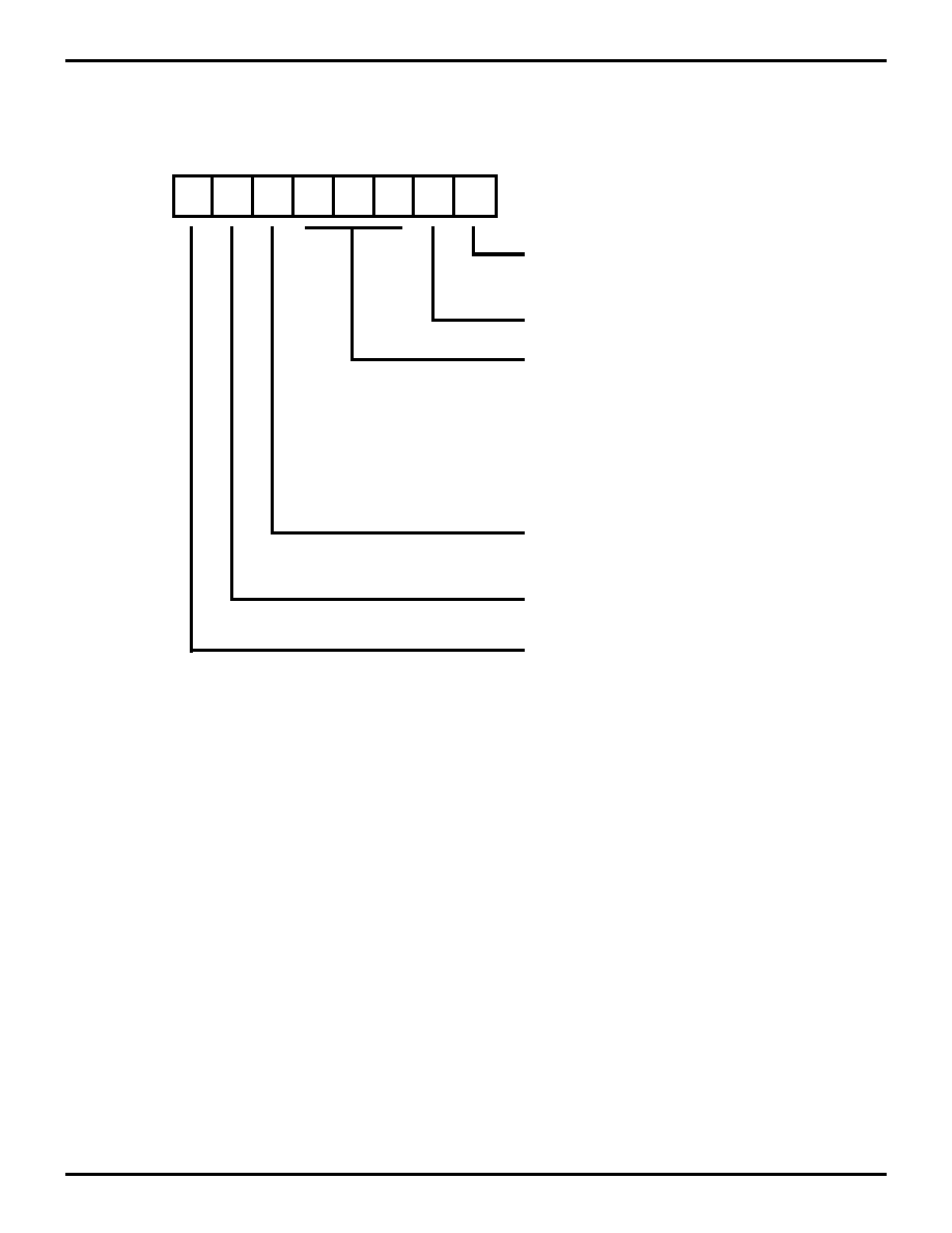
Z86L70/71/75/C71
IR/Low-Voltage Microcontroller
Zilog
1-54
P R E L I M I N A R Y
DS97LVO0500
EXPANDED REGISTER FILE CONTROL REGISTERS (0D) (Continued)
Figure 43. Stop-Mode Recovery Register
((F) 0BH: D6-D0 = Write Only, D7 = Read Only)
D7
D6
D5
D4
D3
D2
D1
D0
SMR (F) 0B
SCLK/TCLK Divide-by-16
0 OFF
1 ON
Reserved (Must be 0)
Stop-Mode Recovery Source
000
001
010
0 11
100
101
11 0
111
Stop Delay
0 OFF
1 ON
Reserved (Must be 0)
Stop Flag
0 POR
1 Stop Recovery**
* Default Setting After Reset
** Default Setting After Reset and Stop-Mode Recovery
**
*
*
POR Only
Reserved
P31
P32
P33
P27
P2 NOR 0-3
P2 NOR 0-7
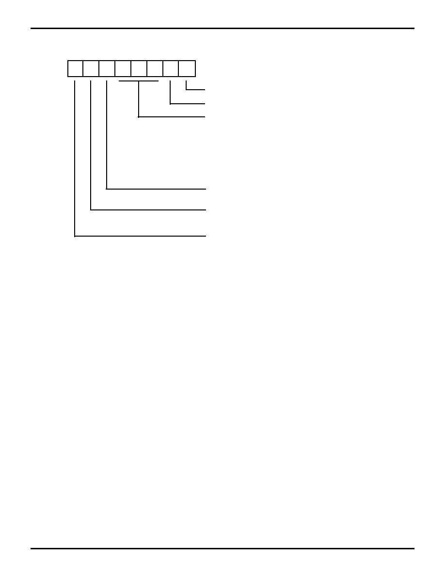
Z86L70/71/75/C71
Zilog
IR/Low-Voltage Microcontroller
DS97LVO0500
P R E L I M I N A R Y
1-55
1
Figure 44. Stop-Mode Recovery Register 2
((0F) 0DH: D2-D4, D6 Write Only)
D7 D6
D5
D4
D3
D2
D1
D0
SMR2 (0F) 0DH
Reserved (Must be 0)
Reserved (Must be 0)
Stop-Mode Recovery Source 2
000 POR only*
001 NAND P20, P21, P22, P23
010 NAND P20, P21, P22, P23, P24, P25, P26, P27
011 NOR P31, P32, P33
100 NAND P31, P32, P33
101 NOR P31, P32, P33, P00, P07
110 NAND P31, P32, P33, P00, P07
111 NAND P31, P32, P33, P20, P21, P22
Reserved
(Must be 0)
Recovery Level
0 Low*
1 High
Reserved (Must be 0)
Note: If used in conjunction with SMR,
either of the two specified events will
cause a Stop-Mode Recovery.
*Default Setting After Reset
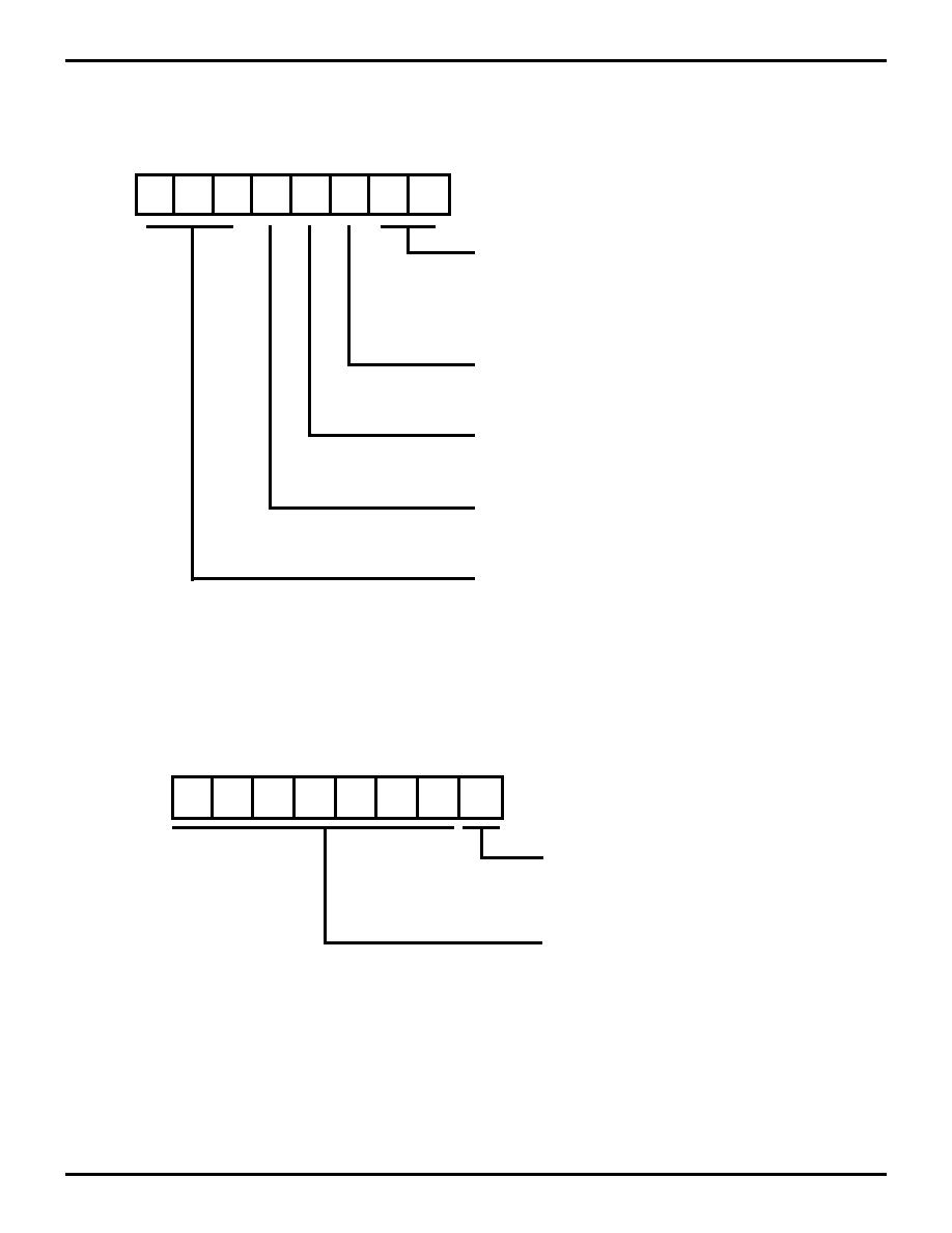
Z86L70/71/75/C71
IR/Low-Voltage Microcontroller
Zilog
1-56
P R E L I M I N A R Y
DS97LVO0500
EXPANDED REGISTER FILE CONTROL REGISTERS (0D) (Continued)
Figure 45. Watch-Dog Timer Mode Register
((F) OFH: Write Only)
Figure 46. Port Configuration Register (PCON)
((0F) OH: Write Only)
D7
D6
D5
D4
D3
D2
D1
D0
WDTMR (0F) 0F
WDT TAP INT RC OSC External Clock
00 5 ms 256 TpC
01 10 ms 512 TpC
10 20 ms 1024 TpC
11 80 ms 4096 TpC
WDT During HALT
0 OFF
1 ON
WDT During STOP
0 OFF
1 ON
XTAL1/INT RC Select for WDT
0 On-Chip RC
1 XTAL
Reserved (Must be 0)
* Default Setting After Reset
*
*
*
*
Reserved (Must be 0)
D7
D6
D5
D4 D3
D2
D1
D0
PCON (0F) 00H
Comparator Output Port 3
0 P34,Standard Output*
1 P34,Comparator Output
* Default Setting After Reset
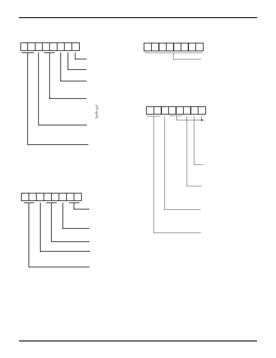
Z86L70/71/75/C71
Zilog
IR/Low-Voltage Microcontroller
DS97LVO0500
P R E L I M I N A R Y
1-57
1
Z8 STANDARD CONTROL REGISTER DIAGRAMS
Figure 47. Port 3 Mode Register
(F7H: Write Only)
Figure 48. Port 0 and 1 Mode Register
(F8H: Write Only)
D7 D6 D5 D4 D3 D2 D1 D0
R247 P3M
0 Port 2 Open Drain*
1 Port 2 Push-pull
0 P32 = Input
P35 = Output **
1 P32 = /DAV0/RDY0
P35 = RDY0//DAV0
0 P31 = Input (TIN)
P36 = Output (TOUT)
1 P31 = /DAV2/RDY2
P36 = RDY2//DAV2
0 = P31, P32 Digital Mode
1 = P31, P32 Analog Mode
00 P33 = Input
P34 = Output **
01 P33 = Input
10 P34 = /DM
P33 = /DAV1/RDY1
P34 = RDY1//DAV1
11
* Default Setting After Result
Note: D0 affects P34, P35 as well as Port 2.
Reserved (Must be 0)
D7
D6
D5
D4
D3
D2
D1
D0
R248 P01M
P00-P03 Mode
00 Output
01 Input*
1X A11-A8
Stack Selection
0 External
1 Internal*
Reserved (Must be 0)
P07-P04 Mode
00 Output
01 Input*
1X A15-A12
External Memory Timing
0 Normal*
1 Extended
* Default Setting After Reset.
Note: Only P00 and P07 are Available on Z86L71.
Figure 49. Port 2 Mode Register
(F8H: Write Only)
Figure 50. Interrupt Priority Register
((0) F9H: Write Only)
D7 D6 D5 D4 D3 D2 D1 D0
P27-P20 I/O Definition
0 Defines Bit as OUTPUT
1 Defines Bit as INPUT*
R246 P2M
*Default Setting After Reset
D7 D6 D5 D4 D3 D2 D1 D0
Interrupt Group Priority
000 Reserved
001 C>A>B
010 A>B>C
011 A>C>B
100 B>C>A
101 C>B>A
110 B>A>C
111 Reserved
IRQ1,IRQ4,Priority
(Group C)
0 IRQ1>IRQ4
1 IRQ4>IRQ1
IRQ0,IRQ2
Priority (Group B)
0 IRQ2>IRQ0
1 IRQ0>IRQ2
IRQ3,IRQ5Priority
(Group A)
0 IRQ5>IRQ3
1 IRQ3>IRQ5
Reserved (Must be 0)
Z86L70/71/75/C71
IR/Low-Voltage Microcontroller
Zilog
1-58
P R E L I M I N A R Y
DS97LVO0500
Figure 51. Interrupt Request Register
((0) FAH: Read/Write)
Figure 52. Interrupt Mask Register
((0) FBH: Read/Write)
Figure 53. Flag Register
((0) FCH: Read/Write)
D7
D6
D5
D4
D3
D2
D1
D0
R250 IRQ
Inter Edge
P31
P32
= 00
P31
P32
= 01
P31
P32
= 10
P31
P32
= 11
IRQ0 = P32 Input
IRQ1 = P33 Input
IRQ2 = P31 Input
IRQ3 = T16_OUT
IRQ4 = T8_OUT
Reserved (Must be 0)
Default Setting After Reset = 0000 0000
D7 D6
D5
D4
D3
D2
D1
D0
Reserved (Must be 0)
1 Enables IRQ4-IRQ0
(D0 = IRQ0)
0 Master Interrupt Disable*
1 Master Interrupt Enable
R251 IMR
* Default Setting After Reset
Reserved (Must be 0)
D7 D6 D5 D4 D3 D2 D1 D0
User Flag F1
User Flag F2
Half Carry Flag
Decimal Adjust Flag
Overflow Tag
Sign Flag
Zero Flag
Carry Flag
R252 FLAGS
Figure 54. Register Pointer
((0) FDH: Read/Write)
Figure 55. Stack Pointer High
((0) FEH: Read/Write)
Figure 56. Stack Pointer Low
((0) FFH: Read/Write)
D7 D6 D5 D4 D3 D2 D1 D0
Expanded Register
Pointer
Working Register
Pointer
R253 RP
Default Setting After
Reset = 0000 0000
D7 D6 D5 D4 D3 D2 D1 D0
Stack Pointer Upper
Byte (SP15-SP8)
R254 SPH
D7 D6 D5 D4 D3 D2 D1 D0
Stack Pointer Lower
Byte (SP7-SP0)
R255 SPL
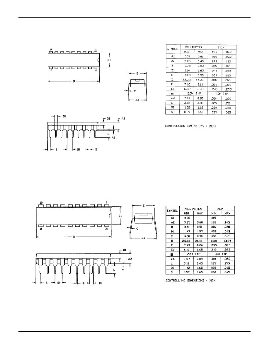
Z86L70/71/75/C71
Zilog
IR/Low-Voltage Microcontroller
DS97LVO0500
P R E L I M I N A R Y
1-59
1
PACKAGE INFORMATION
Figure 57. 18-Pin DIP Pin Assignments
Figure 58. 20-Pin DIP Pin Assignments
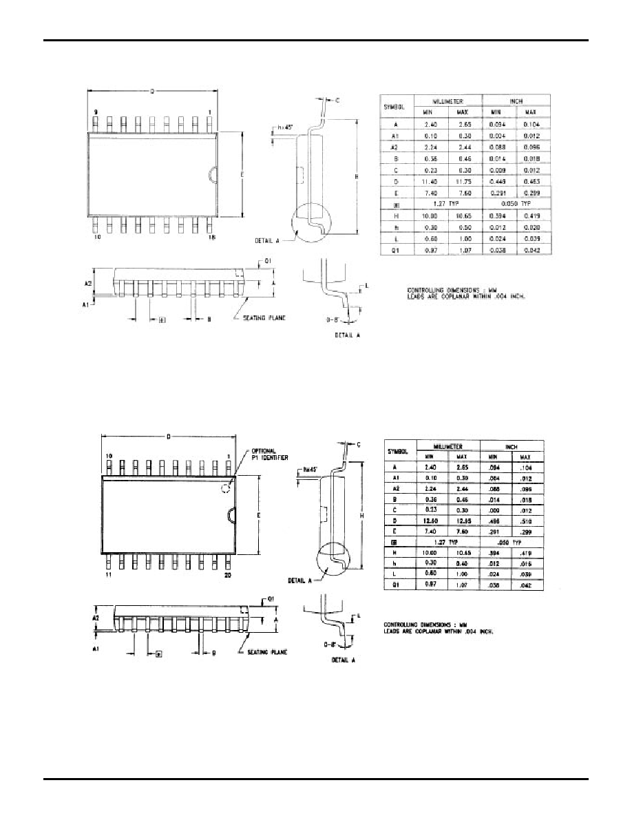
Z86L70/71/75/C71
IR/Low-Voltage Microcontroller
Zilog
1-60
P R E L I M I N A R Y
DS97LVO0500
Figure 59. 18-Pin SOIC Pin Assignments
Figure 60. 20-Pin SOIC Pin Assignments

Z86L70/71/75/C71
Zilog
IR/Low-Voltage Microcontroller
DS97LVO0500
P R E L I M I N A R Y
1-61
1
ORDERING INFORMATION
Z86L70/71/75/C71
8.0 MHz
18-pin DIP
20-pin DIP
Z86L7008PSC
Z86L7108PSC
Z86L7508PSC
18-pin SOIC
20-pin SOIC
Z86L7008SSC
Z86L7108SSC
Z86L7508SSC
16.0 MHz
20-pin DIP
Z86C7116PSC
Codes
Package
P = Plastic DIP
S = SOIC (Small Outline Chip Carrier)
Temperature
Standard = 0
∞
C to +70
∞
C
Environmental
C = Plastic Standard
© 1997 by Zilog, Inc. All rights reserved. No part of this
document may be copied or reproduced in any form or by
any means without the prior written consent of Zilog, Inc.
The information in this document is subject to change
without notice. Devices sold by Zilog, Inc. are covered by
warranty and patent indemnification provisions appearing
in Zilog, Inc. Terms and Conditions of Sale only. Zilog, Inc.
makes no warranty, express, statutory, implied or by
description, regarding the information set forth herein or
regarding the freedom of the described devices from
intellectual property infringement. Zilog, Inc. makes no
warranty of merchantability or fitness for any purpose.
Zilog, Inc. shall not be responsible for any errors that may
appear in this document. Zilog, Inc. makes no commitment
to update or keep current the information contained in this
document.
Zilog's products are not authorized for use as critical
components in life support devices or systems unless a
specific written agreement pertaining to such intended use
is executed between the customer and Zilog prior to use.
Life support devices or systems are those which are
intended for surgical implantation into the body, or which
sustains life whose failure to perform, when properly used
in accordance with instructions for use provided in the
labeling, can be reasonably expected to result in
significant injury to the user.
Zilog, Inc. 210 East Hacienda Ave.
Campbell, CA 95008-6600
Telephone (408) 370-8000
FAX 408 370-8056
Internet: http://www.zilog.com
Example:
Z 86L71 08 P S C
Environmental Flow
Temperature
Package
Speed
Product Number
Zilog Prefix
is a Z86L71, 8 MHz, DIP, 0
∞
C to +70
∞
C, Plastic Standard Flow