DS97LVO0900
P R E L I M I N A R Y
6-1
1
P
RODUCT
S
PECIFICATION
Z86C72/C92/L72/L92
1
IR M
ICROCONTROLLER
FEATURES
s
Expanded Register File Control Registers
s
Low Power Consumption - 40 mW (typical)
s
Three Standby Modes:
�
STOP
�
HALT
�
Low Voltage
s
Automatic External ROM Access Beyond 16K
(Z86LX2/C72 Version)
s
Special Architecture to Automate Both Generation and
Reception of Complex Pulses or Signals:
�
One Programmable 8-Bit Counter/Timer with Two
Capture Register
�
One Programmable 16-Bit Counter/Timer with
One Capture Register
�
Programmable Input Glitch Filter for Pulse
Reception
s
Five Priority Interrupts
�
Three External
�
Two Assigned to Counter/Timers
s
Low Voltage Detection and Standby Mode
s
Programmable Watch-Dog/Power-On Reset Circuits
s
Two Independent Comparators with Programmable
Interrupt Polarity
s
On-Chip Oscillator that Accepts a Crystal, Ceramic
Resonator, LC, RC (mask option), or External Clock
Drive
s
Mask Selectable 200 kOhms Pull-Ups on Ports 0, 2, 3
�
All Eight Port 2 Bits at one time or Not
�
Pull-Ups Automatically Disabled Upon Selecting
Individual Pins as Outputs
s
Maskable Mouse/Trackball Interface on P00 Through
P03 is available on the L72 version.
s
32 kHz Oscillator Mask Option
GENERAL DESCRIPTION
The Z86LX2/CX2 family of IR (Infrared) are ROM/ROM-
less-based members of the Z8
�
MCU single-chip micro-
controller family with 768 bytes of internal RAM. The differ-
entiating factor between these devices is the availability of
RAM, ROM and package options. The use of external
memory enables these Z8 microcontrollers to be used
where code flexibility is required. Offering the 5V versions
(Z86CXX) and gives optimum performance in both the low
and high voltage ranges. Zilog's CMOS microcontrollers
offer fast execution, efficient use of memory, sophisticated
interrupts, input/output bit manipulation capabilities, auto-
mated pulse generation/reception, and internal key-scan
pull-up resistors. The Z86LX2/CX2 product line offers easy
hardware/software system expansion with cost-effective
and low power consumption.
The Z86LX2/CX2 architecture is based on Zilog's 8-bit mi-
crocontroller core with an Expanded Register File to allow
Part
ROM
(KB)
RAM*
(Bytes)
I/O
Voltage Range
Z86C72
16
748
31
4.5V to 5.5V
Z86C92
0
748
31
4.5V to 5.5V
Z86L72
16
748
31
2.0V to 3.9V
Z86L92
0
748
31
2.0V to 3.9V
Note:
*General-Purpose
Z86C72/C92/L72/L92
IR Microcontroller
Zilog
6-2
P R E L I M I N A R Y
DS97LVO0900
GENERAL DESCRIPTION
(Continued)
access to register mapped peripherals, I/O circuits, and
powerful counter/timer circuitry. The Z86C72/C92/L72/L92
offers a flexible I/O scheme, an efficient register and ad-
dress space structure, and a number of ancillary features
that are useful in many consumer, automotive, computer
peripheral, and battery operated hand-held applications.
Many applications demand powerful I/O capabilities. The
Z86LX2/CX2 family fulfills this with three package options
in which the L72 version provides 31 pins of dedicated in-
put and output. These lines are grouped into four ports.
Each port consists of eight lines (Port 3 has seven lines)
and is configurable under software control to provide tim-
ing, status signals, parallel I/O with or without handshake,
and an address/data bus for interfacing external memory.
There are five basic address spaces available to support a
wide range of configurations: Program Memory, Register
File, Expanded Register File, Extended Data RAM and Ex-
ternal Memory. The register file is composed of 256 bytes
of RAM. It includes four I/O port registers, 16 control and
status registers and the rest are General-Purpose regis-
ters. The Extended Data RAM adds 512 bytes of usable
general-purpose registers. The Expanded Register FIle
consists of two additional register groups (F and D).
To unburden the program from coping with such real-time
problems as generating complex waveforms or receiving
and demodulating complex waveform/pulses, the
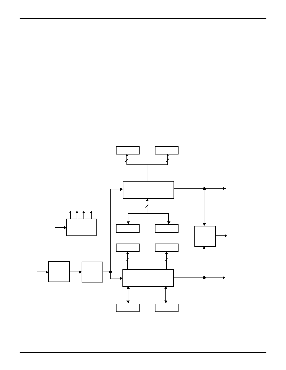
Z86LX2/CX2 family offers a new intelligent counter/timer
architecture with 8-bit and 16-bit counter/timers (Figure 1).
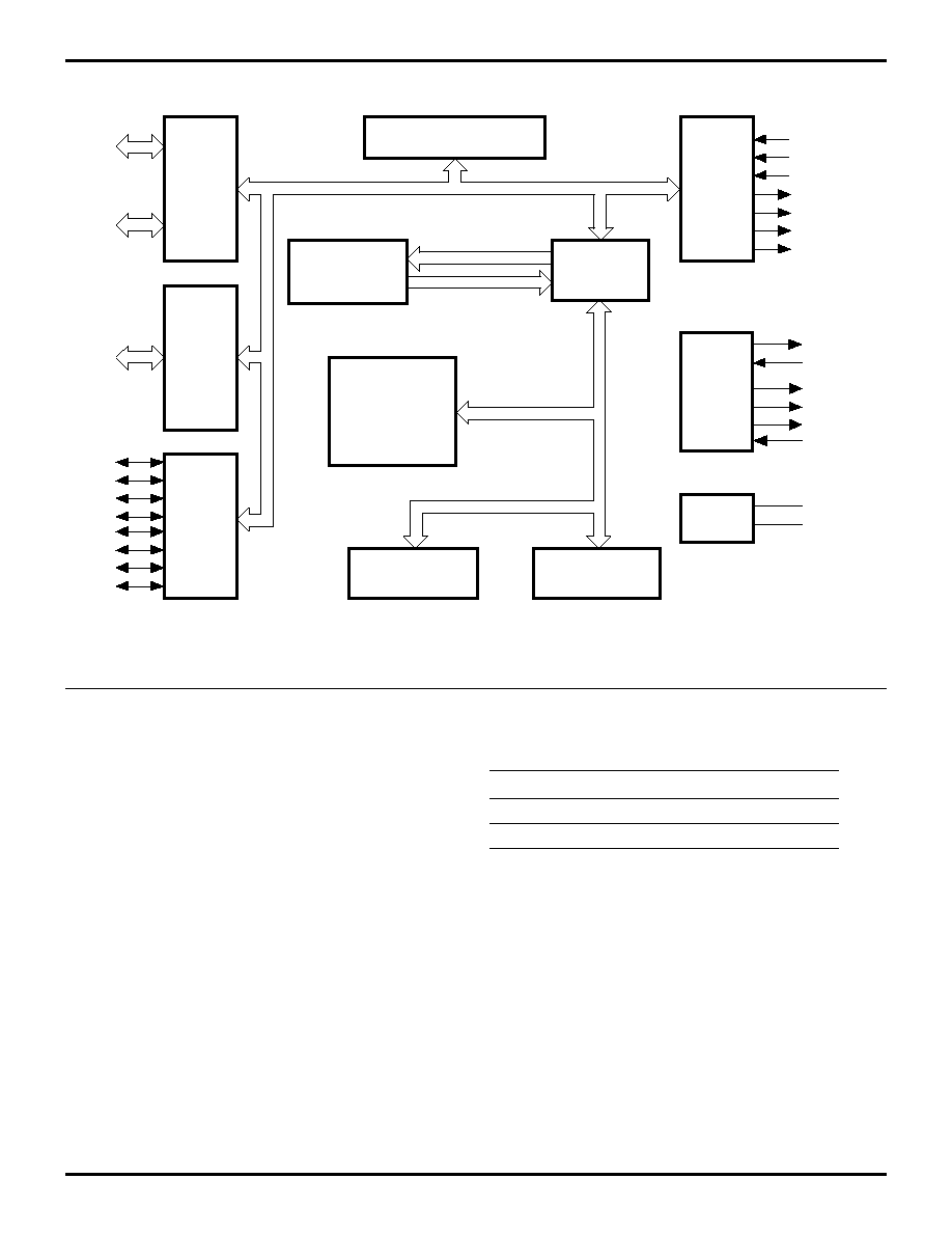
Also included are a large number of user-selectable
modes, and two on-board comparators to process analog
signals with separate reference voltages (Figure 2).
Figure 1. Counter/Timer Block Diagram
HI16
LO16
16-Bit
T16
TC16H
TC16L
HI8
LO8
And/Or
Logic
Clock
Divider
Glitch
Filter
Edge
Detect
Circuit
8-Bit
T8
TC8H
TC8L
8
8
16
8
Input
SCLK
1
2 4
8
Timer 16
Timer 8/16
Timer 8
8
8
8
8
8
Z86C72/C92/L72/L92
Zilog
IR Microcontroller
DS97LVO0900
P R E L I M I N A R Y
6-3
1
Note:
All Signals with a preceding front slash, "/", are ac-
tive Low, e.g., B//W (WORD is active Low); /B/W (BYTE is
active Low, only).
Power connections follow conventional descriptions be-
low:
Figure 2. Functional Block Diagram
Port 0
P00
P01
P02
P03
P04
P05
P06
P07
P10
P11
P12
P13
P14
P15
P16
P17
P20
P21
P22
P23
P24
P25
P26
P27
P31
P32
P33
/AS
/DS
R/W
/RESET
Port 3
Port 1
Port 2
Register File
256 x 8-Bit
ROM
16K/0K x 8
Z8 Core
Register Bus
Internal
Address Bus
Internal Data Bus
Expanded
Register
File
512 x 8-Bit
Expanded
Register Bus
Counter/Timer 8
8-Bit
Counter/Timer 16
16-Bit
Machine
Timing
&
Instruction
Control
Power
XTAL
VDD
VSS
P34
P35
P36
P37
Connection
Circuit
Device
Power
V
CC
V
DD
Ground
GND
V
SS
Z86C72/C92/L72/L92
IR Microcontroller
Zilog
6-4
P R E L I M I N A R Y
DS97LVO0900
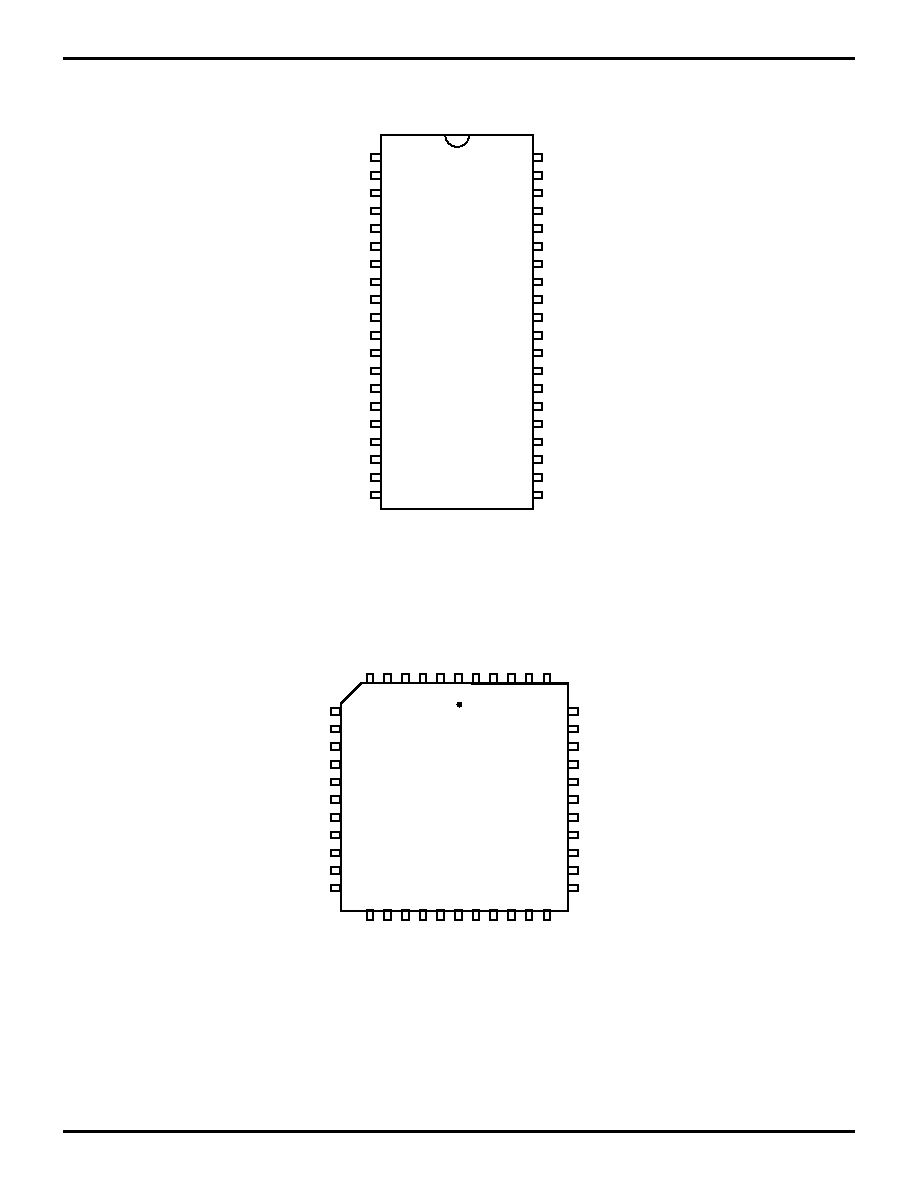
PIN DESCRIPTION
Figure 3. 40-Pin DIP Pin Assignments
R//W
P25
P26
P27
P04
P05
P06
P14
P15
P07
VDD
P16
P17
XTAL2
XTAL1
P31
P32
P33
P34
/AS
/DS
P24
P23
P22
P21
P20
P03
P13
P12
VSS
P02
P11
P10
P01
P00
Pref1
P36
P37
P35
/RESET
40
Z86C72/C92
Z86L72/L92
DIP
1
20
21
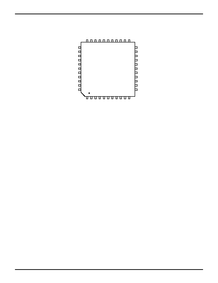
Figure 4. 44-Pin PLCC Pin Assignments
Z86C72/C92
Z86L72/L92
PLCC
7
17
P21
P22
P23
P24
/DS
R//RL
R//W
P25
P26
P27
P04
Pref1
P36
P37
P35
/RESET
VSS
/AS
P34
P33
P32
P31
P05
P06
P14
P15
P07
VDD
VDD
P16
P17
XT
AL2
XT
AL1
P20
P03
P13
P12
VSS
VSS
P02
P11
P10
P01
P00
1
28
18
40
39
29
6