 | –≠–ª–µ–∫—Ç—Ä–æ–Ω–Ω—ã–π –∫–æ–º–ø–æ–Ω–µ–Ω—Ç: Z86L996 | –°–∫–∞—á–∞—Ç—å:  PDF PDF  ZIP ZIP |

ZiLOG Worldwide Headquarters ∑ 532 Race Street ∑ San Jose, CA 95126-3432
Telephone: 408.558.8500 ∑ Fax: 408.558.8300 ∑
www.ZiLOG.com
Preliminary Product Specification
PS003807-1002
Z86D990/Z86D991 OTP and
Z86L99X ROM
Low-Voltage Micro-
controllers with ADC

P R E L I M I N A R Y
PS003807-1002
This publication is subject to replacement by a later edition. To determine whether
a later edition exists, or to request copies of publications, contact:
ZiLOG Worldwide Headquarters
532 Race Street
San Jose, CA 95126-3432
Telephone: 408.558.8500
Fax: 408.558.8300
www.ZiLOG.com
ZiLOG is a registered trademark of ZiLOG Inc. in the United States and in other countries. All other
products and/or service names mentioned herein may be trademarks of the companies with which
they are associated.
Document Disclaimer
© 2002 by ZiLOG, Inc. All rights reserved. Information in this publication concerning the devices,
applications, or technology described is intended to suggest possible uses and may be superseded.
ZiLOG, INC. DOES NOT ASSUME LIABILITY FOR OR PROVIDE A REPRESENTATION OF
ACCURACY OF THE INFORMATION, DEVICES, OR TECHNOLOGY DESCRIBED IN THIS
DOCUMENT. ZiLOG ALSO DOES NOT ASSUME LIABILITY FOR INTELLECTUAL PROPERTY
INFRINGEMENT RELATED IN ANY MANNER TO USE OF INFORMATION, DEVICES, OR
TECHNOLOGY DESCRIBED HEREIN OR OTHERWISE. Except with the express written approval
ZiLOG, use of information, devices, or technology as critical components of life support systems is
not authorized. No licenses or other rights are conveyed, implicitly or otherwise, by this document
under any intellectual property rights.

Z86D990/Z86D991 OTP and Z86L99X ROM
Low-Voltage Microcontrollers with ADC
PS003807-1002
P R E L I M I N A R Y
iii
Table of Contents
Architectural Overview . . . . . . . . . . . . . . . . . . . . . . . . . . . . . . . . . . . . . . . . . . . . 1
Features . . . . . . . . . . . . . . . . . . . . . . . . . . . . . . . . . . . . . . . . . . . . . . . . . . . . . . . 2
Counter/Timers . . . . . . . . . . . . . . . . . . . . . . . . . . . . . . . . . . . . . . . . . . . . . . . 2
Input/Output and Interrupts . . . . . . . . . . . . . . . . . . . . . . . . . . . . . . . . . . . . . . 2
Operating Characteristics . . . . . . . . . . . . . . . . . . . . . . . . . . . . . . . . . . . . . . . 3
User-Programmable Option Bits . . . . . . . . . . . . . . . . . . . . . . . . . . . . . . . . . . 3
Functional Block Diagram . . . . . . . . . . . . . . . . . . . . . . . . . . . . . . . . . . . . . . . . . . 4
Pin Descriptions . . . . . . . . . . . . . . . . . . . . . . . . . . . . . . . . . . . . . . . . . . . . . . . . . 5
Pins Configuration . . . . . . . . . . . . . . . . . . . . . . . . . . . . . . . . . . . . . . . . . . . . . 7
Operational Description . . . . . . . . . . . . . . . . . . . . . . . . . . . . . . . . . . . . . . . . . . . . 9
Central Processing Unit (CPU) Description . . . . . . . . . . . . . . . . . . . . . . . . . . 9
Memory (ROM/OTP and RAM) . . . . . . . . . . . . . . . . . . . . . . . . . . . . . . . . . . 10
Clock Circuit Description . . . . . . . . . . . . . . . . . . . . . . . . . . . . . . . . . . . . . . . 14
Interrupts . . . . . . . . . . . . . . . . . . . . . . . . . . . . . . . . . . . . . . . . . . . . . . . . . . . 15
Reset Conditions . . . . . . . . . . . . . . . . . . . . . . . . . . . . . . . . . . . . . . . . . . . . . 19
Power Management . . . . . . . . . . . . . . . . . . . . . . . . . . . . . . . . . . . . . . . . . . 22
I/O Ports . . . . . . . . . . . . . . . . . . . . . . . . . . . . . . . . . . . . . . . . . . . . . . . . . . . 24
Peripherals . . . . . . . . . . . . . . . . . . . . . . . . . . . . . . . . . . . . . . . . . . . . . . . . . 28
Control and Status Registers . . . . . . . . . . . . . . . . . . . . . . . . . . . . . . . . . . . . . . 52
Register Summary . . . . . . . . . . . . . . . . . . . . . . . . . . . . . . . . . . . . . . . . . . . . 52
Register Error Conditions . . . . . . . . . . . . . . . . . . . . . . . . . . . . . . . . . . . . . . 54
Registers (Grouped by Function) . . . . . . . . . . . . . . . . . . . . . . . . . . . . . . . . 55
Electrical Characteristics . . . . . . . . . . . . . . . . . . . . . . . . . . . . . . . . . . . . . . . . . . 85
Absolute Maximum Ratings . . . . . . . . . . . . . . . . . . . . . . . . . . . . . . . . . . . . . 85
Standard Test Conditions . . . . . . . . . . . . . . . . . . . . . . . . . . . . . . . . . . . . . . 85
DC Characteristics . . . . . . . . . . . . . . . . . . . . . . . . . . . . . . . . . . . . . . . . . . . 86
Analog-to-Digital Converter Characteristics . . . . . . . . . . . . . . . . . . . . . . . . 89
AC Characteristics . . . . . . . . . . . . . . . . . . . . . . . . . . . . . . . . . . . . . . . . . . . . 90
Packaging . . . . . . . . . . . . . . . . . . . . . . . . . . . . . . . . . . . . . . . . . . . . . . . . . . . . . 91
Design Considerations . . . . . . . . . . . . . . . . . . . . . . . . . . . . . . . . . . . . . . . . . . . 94
Ordering Information . . . . . . . . . . . . . . . . . . . . . . . . . . . . . . . . . . . . . . . . . . . . . 95
Precharacterization Product . . . . . . . . . . . . . . . . . . . . . . . . . . . . . . . . . . . . . . . 95

Z86D990/Z86D991 OTP and Z86L99X ROM
Low-Voltage Microcontrollers with ADC
PS003807-1002
P R E L I M I N A R Y
iv
List of Figures
Figure 1. Functional Block Diagram . . . . . . . . . . . . . . . . . . . . . . . . . . . . . . . . . 4
Figure 2. 48-Pin SSOP Pin Assignments . . . . . . . . . . . . . . . . . . . . . . . . . . . . . 5
Figure 3. 40-Pin DIP Pin Assignment . . . . . . . . . . . . . . . . . . . . . . . . . . . . . . . . 6
Figure 4. 28-Pin SOIC/DIP Pin Assignment--User Mode . . . . . . . . . . . . . . . . 7
Figure 5. Program Memory Map . . . . . . . . . . . . . . . . . . . . . . . . . . . . . . . . . . . 12
Figure 6. Standard Z8 Register File (Working Reg. Groups 0≠F, Bank 0) . . . 13
Figure 7. Z8 Expanded Register File Architecture . . . . . . . . . . . . . . . . . . . . . 14
Figure 8. Interrupt Block Diagram . . . . . . . . . . . . . . . . . . . . . . . . . . . . . . . . . . 16
Figure 9. External Interrupt Sources IRQ0≠IRQ2 Block Diagram . . . . . . . . . . 17
Figure 10. IRQ Logic . . . . . . . . . . . . . . . . . . . . . . . . . . . . . . . . . . . . . . . . . . . . . 18
Figure 11. Interrupt Request Timing . . . . . . . . . . . . . . . . . . . . . . . . . . . . . . . . . 18
Figure 12. General Input/Output Pin . . . . . . . . . . . . . . . . . . . . . . . . . . . . . . . . . 26
Figure 13. Analog Comparators . . . . . . . . . . . . . . . . . . . . . . . . . . . . . . . . . . . . 28
Figure 14. ADC Block Diagram . . . . . . . . . . . . . . . . . . . . . . . . . . . . . . . . . . . . . 29
Figure 15. Low-Pass Filter (with 8-MHz Crystal) . . . . . . . . . . . . . . . . . . . . . . . 30
Figure 16. Active Glitch/Power Filter . . . . . . . . . . . . . . . . . . . . . . . . . . . . . . . . 32
Figure 17. I-V Characteristics for the Current Sink Pad P43 . . . . . . . . . . . . . . 34
Figure 18. T
1
Counter/Timer Block Diagram . . . . . . . . . . . . . . . . . . . . . . . . . . . 35
Figure 19. Register File . . . . . . . . . . . . . . . . . . . . . . . . . . . . . . . . . . . . . . . . . . 36
Figure 20. Prescaler 1 Register . . . . . . . . . . . . . . . . . . . . . . . . . . . . . . . . . . . . 36
Figure 21. Counter/Timer 1 Register . . . . . . . . . . . . . . . . . . . . . . . . . . . . . . . . 37
Figure 22. Timer Mode Register . . . . . . . . . . . . . . . . . . . . . . . . . . . . . . . . . . . . 37
Figure 23. Starting the Count . . . . . . . . . . . . . . . . . . . . . . . . . . . . . . . . . . . . . . 38
Figure 24. Counting Modes . . . . . . . . . . . . . . . . . . . . . . . . . . . . . . . . . . . . . . . 39
Figure 25. Timer Mode Register T
OUT
Operation . . . . . . . . . . . . . . . . . . . . . . . 40
Figure 26. Counter/Timer Output Using T
OUT
. . . . . . . . . . . . . . . . . . . . . . . . . 41
Figure 27. Internal Clock Output Using T
OUT
. . . . . . . . . . . . . . . . . . . . . . . . . . 41
Figure 28. Timer Mode Register T
IN
Operation . . . . . . . . . . . . . . . . . . . . . . . . 42
Figure 29. Prescaler 1 T
IN
Operation . . . . . . . . . . . . . . . . . . . . . . . . . . . . . . . . 42
Figure 30. External Clock Input Mode . . . . . . . . . . . . . . . . . . . . . . . . . . . . . . . 43
Figure 31. Gated Clock Input Mode . . . . . . . . . . . . . . . . . . . . . . . . . . . . . . . . . 43
Figure 32. Triggered Clock Mode . . . . . . . . . . . . . . . . . . . . . . . . . . . . . . . . . . . 44
Figure 33. Counter/Timer Architecture . . . . . . . . . . . . . . . . . . . . . . . . . . . . . . . 46
Figure 34. Transmit Mode Flowchart . . . . . . . . . . . . . . . . . . . . . . . . . . . . . . . . 48

Z86D990/Z86D991 OTP and Z86L99X ROM
Low-Voltage Microcontrollers with ADC
PS003807-1002
P R E L I M I N A R Y
v
Figure 35. Demodulation Mode Flowchart . . . . . . . . . . . . . . . . . . . . . . . . . . . . 50
Figure 36. Test Load Diagram . . . . . . . . . . . . . . . . . . . . . . . . . . . . . . . . . . . . . 86
Figure 37. 48-Pin SSOP . . . . . . . . . . . . . . . . . . . . . . . . . . . . . . . . . . . . . . . . . . 91
Figure 38. 40-Pin PDIP . . . . . . . . . . . . . . . . . . . . . . . . . . . . . . . . . . . . . . . . . . . 92
Figure 39. 28-Pin PDIP . . . . . . . . . . . . . . . . . . . . . . . . . . . . . . . . . . . . . . . . . . . 92
Figure 40. 28-Pin SOIC . . . . . . . . . . . . . . . . . . . . . . . . . . . . . . . . . . . . . . . . . . 93

Z86D990/Z86D991 OTP and Z86L99X ROM
Low-Voltage Microcontrollers with ADC
PS003807-1002
P R E L I M I N A R Y
vi
List of Tables
Table 1.
Z86L99/Z86D99 Feature Comparison . . . . . . . . . . . . . . . . . . . . . . . . 1
Table 2.
Pin Descriptions . . . . . . . . . . . . . . . . . . . . . . . . . . . . . . . . . . . . . . . . . 7
Table 3.
Interrupt Types, Sources, and Vectors . . . . . . . . . . . . . . . . . . . . . . 15
Table 4.
Interrupt Edge Select for External Interrupts . . . . . . . . . . . . . . . . . . 17
Table 5.
Control and Status Register Reset Conditions . . . . . . . . . . . . . . . . 20
Table 6.
Clock Status in Operating Modes . . . . . . . . . . . . . . . . . . . . . . . . . . 22
Table 7.
Special Port Pin Functions . . . . . . . . . . . . . . . . . . . . . . . . . . . . . . . 27
Table 8.
Active Glitch/Filter Specifications (Preliminary) . . . . . . . . . . . . . . . . 32
Table 9.
Current Sink Pad P43 Specifications (Preliminary) . . . . . . . . . . . . . 33
Table 10. I/O Port Registers (Group 0, Bank 0, Registers 0≠F) . . . . . . . . . . . 52
Table 11. Timer Control Registers (Group 0, Bank D, Registers 0≠F) . . . . . . 53
Table 12. Control and Status Registers (Group F, Bank 0,
Registers 0≠F) . . . . . . . . . . . . . . . . . . . . . . . . . . . . . . . . . . . . . . . . . 53
Table 13. SMR and Port Mode Registers (Group 0, Bank F,
Registers 0≠F) . . . . . . . . . . . . . . . . . . . . . . . . . . . . . . . . . . . . . . . . . 54
Table 14. Register Description Locations . . . . . . . . . . . . . . . . . . . . . . . . . . . . 55
Table 15. FLAGS Register [Group/Bank F0h, Register C (R252)] . . . . . . . . . 57
Table 16. RP Register [Group/Bank F0h, Register D (R253)] . . . . . . . . . . . . . 58
Table 17. SP Register [Group/Bank F0h, Register F (R255)] . . . . . . . . . . . . . 59
Table 18. LB Register (Group/Bank 0Dh, Register C) . . . . . . . . . . . . . . . . . . . 60
Table 19. ADCCTRL Register (Group/Bank 0Fh, Register 8) . . . . . . . . . . . . . 61
Table 20. ADCDATA Register (Group/Bank 00h, Register 7) . . . . . . . . . . . . . 62
Table 21. IMR (Group/Bank 0Fh, Register B) . . . . . . . . . . . . . . . . . . . . . . . . . 63
Table 22. IPR (Group/Bank 0Fh, Register 9) . . . . . . . . . . . . . . . . . . . . . . . . . 64
Table 23. IRQ (Group/Bank 0Fh, Register A) . . . . . . . . . . . . . . . . . . . . . . . . . 65
Table 24. P456CON Register (Group/Bank 0Fh, Register 0) . . . . . . . . . . . . . 67
Table 25. P3M Register [Group/Bank F0h, Register 7 (R247)] . . . . . . . . . . . . 68
Table 26. P2 Register [Group/Bank 00h, Register 2 (R2)] . . . . . . . . . . . . . . . 68
Table 27. P2M Register [Group/Bank F0h, Register 6 (R246)] . . . . . . . . . . . . 68
Table 28. P4 Register [Group/Bank 00h, Register 4 (R4)] . . . . . . . . . . . . . . . 69
Table 29. P4M Register (Group/Bank 0Fh, Register 2) . . . . . . . . . . . . . . . . . . 69
Table 30. P5 Register [Group/Bank 00h, Register 5 (R5)] . . . . . . . . . . . . . . . 70
Table 31. P5M Register (Group/Bank 0Fh, Register 4) . . . . . . . . . . . . . . . . . . 70
Table 32. P6 Register [Group/Bank 00h, Register 6 (R6)] . . . . . . . . . . . . . . . 71

Z86D990/Z86D991 OTP and Z86L99X ROM
Low-Voltage Microcontrollers with ADC
PS003807-1002
P R E L I M I N A R Y
vii
Table 33. P6M Register (Group/Bank 0Fh, Register 6) . . . . . . . . . . . . . . . . . . 71
Table 34. T1 Register [Group/Bank F0h, Register 2 (R242)] . . . . . . . . . . . . . 72
Table 35. TMR Register [Group/Bank F0h, Register 1 (R241)] . . . . . . . . . . . . 72
Table 36. PRE1 Register [Group/Bank F0h, Register 3 (R243)] . . . . . . . . . . . 73
Table 37. CTR1 Register (In Transmit Mode)
(Group/Bank 0Dh, Register 1) . . . . . . . . . . . . . . . . . . . . . . . . . . . . . 74
Table 38. CTR1 Register (in Demodulation Mode)
(Group/Bank 0Dh, Register 1) . . . . . . . . . . . . . . . . . . . . . . . . . . . . . 75
Table 39. CTR3 Register (Group/Bank 0Dh, Register 3) . . . . . . . . . . . . . . . . 76
Table 40. CTR0 Register (Group/Bank 0Dh, Register 0) . . . . . . . . . . . . . . . . 77
Table 41. HI8 Register (Group/Bank 0Dh, Register B) . . . . . . . . . . . . . . . . . . 78
Table 42. LO8 Register (Group/Bank 0Dh, Register A) . . . . . . . . . . . . . . . . . . 78
Table 43. TC8H Register (Group/Bank 0Dh, Register 5) . . . . . . . . . . . . . . . . 79
Table 44. TC8L Register (Group/Bank 0Dh, Register 4) . . . . . . . . . . . . . . . . . 79
Table 45. CTR2 Register (Group/Bank 0Dh, Register 2) . . . . . . . . . . . . . . . . 80
Table 46. HI16 Register (Group/Bank 0Dh, Register 9) . . . . . . . . . . . . . . . . . 81
Table 47. LO16 Register (Group/Bank 0Dh, Register 8) . . . . . . . . . . . . . . . . . 81
Table 48. TC16H Register (Group/Bank 0Dh, Register 7) . . . . . . . . . . . . . . . 82
Table 49. TC16L Register (Group/Bank 0Dh, Register 6) . . . . . . . . . . . . . . . . 82
Table 50. SMR Register (Group/Bank 0Fh, Register B) . . . . . . . . . . . . . . . . . 83
Table 51. P2SMR Register (Group/Bank 0Fh, Register 1) . . . . . . . . . . . . . . . 84
Table 52. P5SMR Register (Group/Bank 0Fh, Register 5) . . . . . . . . . . . . . . . 84
Table 53. Absolute Maximum Ratings . . . . . . . . . . . . . . . . . . . . . . . . . . . . . . . 85
Table 54. DC Characteristics for the Z86D99X (OTP Only) . . . . . . . . . . . . . . 87
Table 55. DC Characteristics for the Z86L99X (Mask Only) . . . . . . . . . . . . . . 88
Table 56. Analog-to-Digital Converter Characteristics . . . . . . . . . . . . . . . . . . . 89
Table 57. AC Characteristics . . . . . . . . . . . . . . . . . . . . . . . . . . . . . . . . . . . . . . 90

Z86D990/Z86D991 OTP and Z86L99X ROM
Low-Voltage Microcontrollers with ADC
PS003807-1002
P R E L I M I N A R Y
1
Architectural Overview
The Z86D99 is a low-voltage general-purpose one-time programmable (OTP) Z8
Æ
microcontroller with an integrated four-channel 8-bit sigma delta analog-to-digital
converter. The Z86L99 is the read-only memory (ROM) version of this controller.
The Z86D99/Z86L99 family is designed to be used in a wide variety of embedded
control applications including battery chargers, home appliances, infrared (IR)
remote controls, security systems, and wireless keyboards.
It has three counter/timers, a general-purpose 8-bit counter/timer with a 6-bit pres-
caler and an 8-bit/16-bit counter/timer pair that can be used individually for gen-
eral-purpose timing or as a pair to automate the generation and reception of
complex pulses or signals. Unique features of the Z86D99/Z86L99 family of prod-
ucts include 489 bytes of general-purpose random-access memory (RAM), 256
bytes of which are mapped into the program memory space and can be used to
store data variables or as executable RAM, a low-battery detection flag, and a
controlled current output pin, which is a regulated current source that sinks a pre-
defined current (I
CCO
). Table 1 highlights the basic product features of these
microcontrollers.
The Z8 microcontroller core offers more flexibility and performance than accumu-
lator-based microcontrollers. All 256 general-purpose registers, including dedi-
cated input/output (I/O) port registers, can be used as accumulators. This unique
register-to-register architecture avoids accumulator bottlenecks for high code effi-
ciency. The registers can be used as address pointers for indirect addressing, as
index registers, or for implementing an on-chip stack.
The Z8 has a sophisticated interrupt structure and automatically saves the pro-
gram counter and status flags on the stack for fast context-switching. Speed of
execution and smooth programming are also supported by a "working register
area" with short 4-bit register addresses.
Table 1. Z86L99/Z86D99 Feature Comparison
Pins
I/O
Memory
(Bytes)
Operating
Voltage (V)
ADC
Timers
Watch-Dog
Timer
Z86D990
40/48
32
32K OTP
3.0≠5.5
4 channel
3
Yes
Z86D991
28
24
32K OTP
3.0≠5.5
--
3
Yes
Z86L990
40/48
32
16K ROM
2.3≠5.5
4 channel
3
Yes
Z86L991
28
24
16K ROM
2.3≠5.5
--
3
Yes
Z86L996
28
24
4K ROM
2.3≠5.5
--
3
Yes
Z86L997
28
24
8K ROM
2.3≠5.5
--
3
Yes

Z86D990/Z86D991 OTP and Z86L99X ROM
Low-Voltage Microcontrollers with ADC
PS003807-1002
P R E L I M I N A R Y
2
The Z8 instruction set, consisting of 43 basic instructions, is optimized for high-
code density and reduced execution time. It is similar in form to the ZiLOG Z80
instruction set. The eight instruction types and six addressing modes together
with the ability to operate on bits, 4-bit nibbles or binary coded decimal (BCD) dig-
its, 8-bit bytes, and 16-bit words, make for a code-efficient, flexible microcontroller.
Features
∑
Four-channel, 8-bit sigma delta analog-to-digital (A/D) converter with external
voltage references (not available in the 28-pin configuration)
∑
Two independent analog comparators
∑
Controlled current output
∑
489 bytes of RAM
≠ 233 bytes of general-purpose register-based RAM
≠ 256 bytes of RAM mapped into the program memory space that can be
used as data RAM or executable RAM
∑
32 Kbytes of OTP memory (Z86D99X)
∑
16 Kbytes of ROM (Z86L99X)
Counter/Timers
∑
Special architecture to automate generation and reception of complex pulses
or signals:
≠ Programmable 8-bit counter/timer (T8) with two 8-bit capture registers and
two 8-bit load registers
≠ Programmable 16-bit counter/timer (T16) with one 16-bit capture register
pair and one 16-bit load register pair
≠ Programmable input glitch filter for pulse reception
∑
One general-purpose 8-bit counter/timer (T1) with 6-bit prescaler
Input/Output and Interrupts
∑
Thirty-two I/Os, twenty-nine of which are bidirectional I/Os with programmable
resistive pull-up transistors (24 I/Os are available in the 28-pin configuration)
∑
Sixteen I/Os are selectable as stop-mode recovery sources
∑
Six interrupt vectors with nine interrupt sources
≠ Three external sources
≠ Two comparator interrupts

Z86D990/Z86D991 OTP and Z86L99X ROM
Low-Voltage Microcontrollers with ADC
PS003807-1002
P R E L I M I N A R Y
3
≠ Three timer interrupts
≠ One low-battery detector flag
Operating Characteristics
∑
8-MHz operation
∑
3.0 V to 5.5 V operating voltage (Z86D990/Z86D991)
∑
2.3 V to 5.5 V operating voltage (Z86L990/Z86L991)
∑
Low power consumption with three standby modes:
≠ Stop
≠ Halt
≠ Low Voltage Standby
∑
Low-battery detection flag
∑
Low-voltage protection circuit (also known as V
BO
, or voltage brownout,
circuit)
∑
Watch-dog timer and power-on reset circuits
User-Programmable Option Bits
∑
Clock source--RC/other (LC, resonator, or crystal)
∑
Watch-dog timer permanently enable
∑
32-kHz crystal
∑
Port 20≠27 pull-up resistive transistor
∑
Port 40≠42 pull-up resistive transistor
∑
Port 44≠47 pull-up resistive transistor
∑
Port 50≠51 pull-up resistive transistor
∑
Port 54≠57 pull-up resistive transistor
∑
Port 60≠63 pull-up resistive transistor (not available in Z86D991/Z86L991)
∑
Port 64≠67 pull-up resistive transistor (not available in Z86D991/Z86L991)
∑
P43 high impedance in STOP mode (available in OTP only)
Force P43 to output a 1 in the open-drain configuration
Z86D990/Z86D991 OTP and Z86L99X ROM
Low-Voltage Microcontrollers with ADC
PS003807-1002
P R E L I M I N A R Y
4
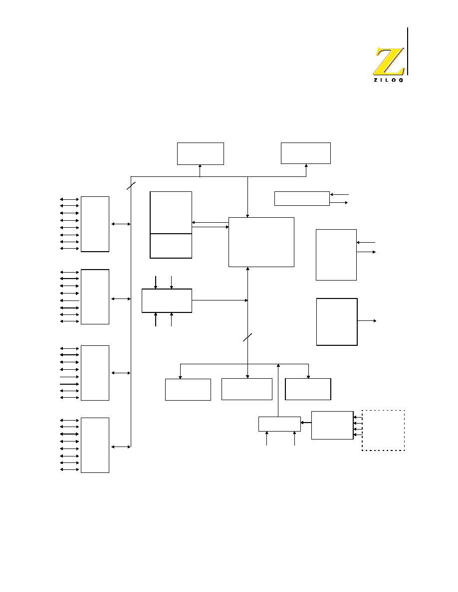
Functional Block Diagram
Figure 1 shows the functional block diagram for the microcontrollers.
Figure 1. Functional Block Diagram
Register File
256 x 8-bit
Z8 Core
V
DD_padring
***
V
DD_CORE
Program
Memory
256 Bytes
Two Analog
Comparators
16-Bit C/T
(Modulation)
MUX
8-Bit A/D
ADC0/P44
ADC1/P45
ADC2/P46
ADC3/P47
Port 2
Port 6
**
Port 5
Port 4
7
0
7
0
7
0
7
0
Power Filter
8
Expanded
Register File
8
8-Bit C/T
(General)
8-Bit C/T
(Carrier)
V
Ref≠
V
Ref+
Machine
Timing
and
Instruction
Control
XTAL 1
XTAL 2
*Controlled Current Output
*
Controlled
Current
Output
P43
P53
CREF2
CREF1
P50
P52
CIN2
CIN1
P51
**P6 is only in the Z86L990/Z86D990.
ADC is only in the Z86L990/Z86D990.
Program memory is as follows:
Z86D990
32K OTP
Z86D991
32K OTP
Z86L990
16K ROM
Z86L991
16K ROM
***In the 28-pin package, V
DD_padring
and V
DD_CORE
are bonded together.
Z86D990/Z86D991 OTP and Z86L99X ROM
Low-Voltage Microcontrollers with ADC
PS003807-1002
P R E L I M I N A R Y
5
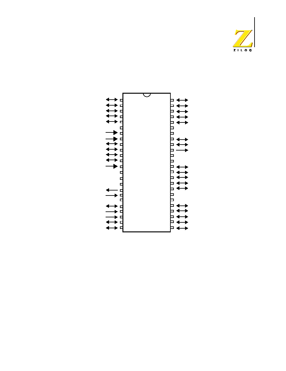
Pin Descriptions
Figure 2 through Figure 4 show the pin names and locations.
Figure 2. 48-Pin SSOP Pin Assignments
P62
P63
P25
P26
P27
NC
AV
SS
V
REF-
P44
P45
P46
P47
V
REF+
AV
DD
V
DD_CORE
V
DD_padring
XTAL2
XTAL1
NC
P51
P52
P53
P54
P64
P61
P60
P24
P23
P22
NC
NC
P21
P20
P43
VSS
VSS
P42
P41
P40
P50
P56
NC
NC
P57
P55
P67
P66
P65
48
Z86D990/
Z86L990
1
24
25
2
3
4
5
6
7
8
9
10
11
12
13
14
15
16
17
18
19
20
21
22
23
46
45
44
43
42
41
40
39
38
37
36
35
34
33
32
31
30
29
281
27
26
47
Notes:
1. Both V
SS
pins must be connected to ground.
2. NC is no connection to the die.
3. AV
DD
must be connected to V
DD_CORE
and a 10-
µ
F capacitor for good A/D conversion.
4. Power must be connected to V
DD_padring
. Current passes to V
DD_CORE
through the internal
power filter.
Z86D990/Z86D991 OTP and Z86L99X ROM
Low-Voltage Microcontrollers with ADC
PS003807-1002
P R E L I M I N A R Y
6
Figure 3. 40-Pin DIP Pin Assignment
P62
P63
P25
P26
P27
AV
SS
VRef≠
P44/ADC0
P45/ADC1
P46/ADC2
P47/ADC3
V
Ref+
AVDD/V
DD_CORE
V
DD_padring
XTAL2
XTAL1
P51/CIN1/Captive Timer Input
P52/CIN2/T1 Timer Input (TIN)
P53/CREF2
P54/COUT1
P61
P60
P24
P23
P22
P21
P20
P43/Combined T8 T16 Output
V
SS
P42
P41/T16 Output
P40/T8 Output
P50/CREF1
P56/T1 Timer Output
P57
P55/COUT2
P67
P66
P65
P64
40
Z86D990/
Z86L990
1
20
21
2
3
4
5
6
7
8
9
10
11
12
13
14
15
16
17
18
19
39
38
37
36
35
34
33
32
31
30
29
28
27
26
25
24
23
22
Notes:
1. AV
DD
must be connected to V
DD_CORE
and a 10-
µ
F capacitor for good A/D conversion.
2. Power must be connected to V
DD_padring
. Current passes to V
DD_CORE
through the internal
power filter.
Z86D990/Z86D991 OTP and Z86L99X ROM
Low-Voltage Microcontrollers with ADC
PS003807-1002
P R E L I M I N A R Y
7
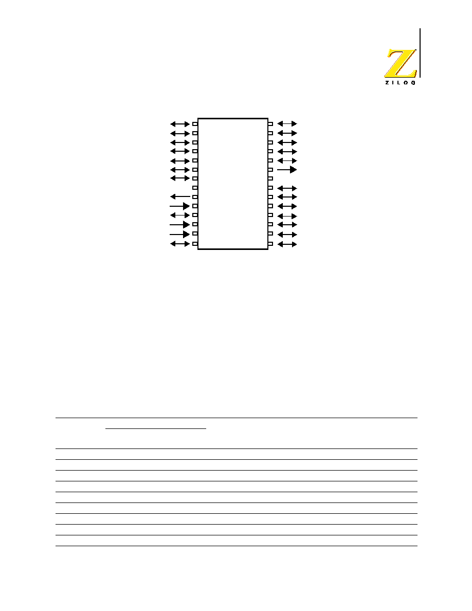
Figure 4. 28-Pin SOIC/DIP Pin Assignment--User Mode
Pins Configuration
Table 2 describes the pins.
Table 2. Pin Descriptions
Pin #
Symbol
28
PDIP/SOIC
40
PDIP
48
SSOP
Direction Description
P20
24
34
40
I/O
Port 2 Bit 0
P21
25
35
41
I/O
Port 2 Bit 1
P22
26
36
44
I/O
Port 2 Bit 2
P23
27
37
45
I/O
Port 2 Bit 3
P24
28
38
46
I/O
Port 2 Bit 4
P25
1
3
3
I/O
Port 2 Bit 5
P26
2
4
4
I/O
Port 2 Bit 6
P27
3
5
5
I/O
Port 2 Bit 7
P40
19
29
34
I/O
Port 4 Bit 0, T8 Output
P25
P26
P27
P44/ADC0
P45/ADC1
P46/ADC2
P47/ADC3
V
DD
*
XTAL2
XTAL1
P51/CIN1/Capture Timer Input
P52/CIN2/T1 Timer Input
P53/CREF2
P54/COUT1
P24
P23
P22
P21
P20
P43/Combined T8 T16 Output
V
SS
**
P42
P41/T16 Output
P40/T8 Output
P50/CREF1
P56/T1 Timer Output
P57
P55/COUT2
Z86D991/
Z86L991
28
27
26
25
24
23
22
21
20
19
18
17
16
15
1
2
3
4
5
6
7
8
9
10
11
12
13
14
Notes:
1. P43 is a controlled current output.
2. P54, P55, P56, and P57 are high drive
outputs.
* V
DD
= V
DD_CORE
+ V
DD_padring
+ AV
DD

Z86D990/Z86D991 OTP and Z86L99X ROM
Low-Voltage Microcontrollers with ADC
PS003807-1002
P R E L I M I N A R Y
8
P41
20
30
35
I/O
Port 4 Bit 1, T16 Output
P42
21
31
36
I/O
Port 4 Bit 2
P43
23
33
39
Output
T8/T16 Output, Controlled current output
P44
4
8
9
I/O
Port 4 Bit 4, A/D Channel 0*
P45
5
9
10
I/O
Port 4 Bit 5, A/D Channel 1*
P46
6
10
11
I/O
Port 4 Bit 6, A/D Channel 2*
P47
7
11
12
I/O
Port 4 Bit 7, A/D Channel 3*
P50, CREF1 18
28
33
I/O
Port 5 Bit 0, Comparator 1 reference
P51, CIN1
11
17
20
I/O
Port 5 Bit 1, Capture timer input, IRQ
2
P52, CIN2
12
18
21
Input
Port 5 Bit 2, Timer 1 timer input, IRQ
0
P53, CREF2 13
19
22
Input
Port 5 Bit 3, Comparator 2 reference, IRQ
1
P54
14
20
23
I/O
Port 5 Bit 4, High drive output
P55
15
25
28
I/O
Port 5 Bit 5, High drive output
P56
17
27
32
I/O
Port 5 Bit 6, Timer 1 output, High drive output
P57
16
26
29
I/O
Port 5 Bit 7, High drive output
P60
39
47
I/O
Port 6 Bit 0
P61
40
48
I/O
Port 6 Bit 1
P62
1
1
I/O
Port 6 Bit 2
P63
2
2
I/O
Port 6 Bit 3
P64
21
24
I/O
Port 6 Bit 4
P65
22
25
I/O
Port 6 Bit 5
P66
23
26
I/O
Port 6 Bit 6
P67
24
27
I/O
Port 6 Bit 7
XTAL1
10
16
18
Input
Crystal, Oscillator clock
XTAL2
9
15
17
Output
Crystal, Oscillator clock
AV
DD
13
14
Analog power supply
V
DD_CORE
13
15
Z8 core power supply
AV
SS
6
7
Analog ground
V
Ref≠
7
8
Input
A/D converter lower reference
V
Ref+
12
13
Input
A/D converter upper reference
V
DD_padring
8**
14
16
Power supply (pad ring)
V
SS
22**
32
37, 38
Ground
Notes:
*A/D converter is not available in the 28-pin configuration.
**In the 28-pin configuration, all three (core, pad ring, and analog) powers are tied together.
Table 2. Pin Descriptions (Continued)
Pin #
Symbol
28
PDIP/SOIC
40
PDIP
48
SSOP
Direction Description

Z86D990/Z86D991 OTP and Z86L99X ROM
Low-Voltage Microcontrollers with ADC
PS003807-1002
P R E L I M I N A R Y
9
Operational Description
Central Processing Unit (CPU) Description
The Z8 architecture is characterized by a flexible I/O scheme, an efficient register
and address space structure and a number of ancillary features for cost-sensitive,
high-volume embedded control applications. ROM-based products are geared for
high-volume production (where the software is stable) and one-time programma-
ble equivalents for prototyping as well as volume production where time to market
or code flexibility is critical.
Architecture Type
The Z8 register-oriented architecture centers around an internal register file com-
posed of 256 consecutive bytes, known as the standard register file. The standard
register file consists of 4 I/O port registers (R2, R4, R5, and R6), 12 control and
status registers, 233 general-purpose registers, and 7 registers reserved for future
expansion. In addition to the standard register file, the Z86D99/Z86L99 family
uses 21 control and status registers located in the Z8 expanded register file. Any
general-purpose register can be used as an accumulator and address pointer or
an index, data, or stack register.
All active registers can be referenced or modified by any instruction that accesses
an 8-bit register, without the requirement for special instructions. Registers
accessed as 16 bits are treated as even-odd register pairs. In this case, the data's
most significant byte (MSB) is stored in the even-numbered register, while the
least significant byte (LSB) goes into the next higher odd-numbered register.
The Z8 CPU has an instruction set designed for the large register file. The instruc-
tion set provides a full compliment of 8-bit arithmetic and logical operations. BCD
operations are supported using a decimal adjustment of binary values, and 16-bit
quantities for addresses and counters can be incremented and decremented. Bit
manipulation and Rotate and Shift instructions complete the data-manipulation
capabilities of the Z8 CPU. No special I/O instructions are necessary because the
I/O is mapped into the register file.
CPU Control Registers
The standard Z8 control registers govern the operation of the CPU. Any instruc-
tion which references the register file can access these control registers. The fol-
lowing are available control registers:
∑
Register Pointer (RP)
∑
Stack Pointer (SP)
∑
Program Control Flags (FLAGS)

Z86D990/Z86D991 OTP and Z86L99X ROM
Low-Voltage Microcontrollers with ADC
PS003807-1002
P R E L I M I N A R Y
10
∑
Interrupt Control (IPR, IMR, and IRQ)
∑
Stop Mode Recovery (SMR, P2SMR, and P5SMR)
∑
Low-Battery Detect (LB) Flag
The Z8 uses a 16-bit Program Counter (PC) to determine the sequence of current
program instructions. The PC is not an addressable register.
Peripheral registers are used to transfer data, configure the operating mode, and
control the operation of the on-chip peripherals. Any instruction that references
the register file can access the peripheral registers. The following are peripheral
control registers:
∑
Analog/Digital Converter (ADCCTRL and ADCDATA)
∑
T1 Timer/Counter (TMR, T1, and PRE1)
∑
T8 Timer/Counter (CTR0, HI8, LO8, TC8H, and TC8L)
∑
T16 Timer/Counter (CTR2, HI16, LO16, TC16H, and TC16L)
∑
T8/T16 Control Registers (CTR1and CTR3)
In addition, the four port registers are considered to be peripheral registers. The
following are port control registers:
∑
Port Configuration Registers (P456CON and P3M)
∑
Port 2 Control and Mode Registers (P2 and P2M)
∑
Port 4 Control and Mode Registers (P4 and P4M)
∑
Port 5 Control and Mode Registers (P5 and P5M)
∑
Port 6 Control and Mode Registers (P6 and P6M)
The functions and applications of the control and peripheral registers are
explained in "Control and Status Registers" on page 52.
Memory (ROM/OTP and RAM)
There are four basic address spaces available to support a wide range of configu-
rations:
∑
Program memory (on-chip)
∑
Standard register file
∑
Expanded register file
∑
Executable RAM
The Z8 standard register file totals up to 256 consecutive bytes organized as 16
groups of 16 eight-bit registers. These registers consist of I/O port registers,

Z86D990/Z86D991 OTP and Z86L99X ROM
Low-Voltage Microcontrollers with ADC
PS003807-1002
P R E L I M I N A R Y
11
general-purpose RAM registers, and control and status registers. Every RAM reg-
ister acts like an accumulator, speeding instruction execution and maximizing cod-
ing efficiency. Working register groups allow fast context switching.
The standard register file of the Z8 (known as Bank 0) has been expanded to form
16 expanded register file (ERF) banks. The expanded register file allows for addi-
tional system control registers and for the mapping of additional peripheral
devices into the register area. Each ERF bank can potentially consist of up to 256
registers (the same amount as in the standard register file) that can then be
divided into 16 working register groups. Currently, only Group 0 of ERF Banks F
and D (
0Fh
and
0Dh
) has been implemented.
In addition to the standard program memory and the RAM register files, the
Z86D99/Z86L99 family also has 256 bytes of executable RAM that has been
mapped into the upper 256 bytes of the program memory address space (
FF00h
≠
FFFFh
). Data can be written to the executable RAM by using the LDC instruction.
Program Memory Structure
The first 12 bytes of program memory are reserved for the interrupt vectors.
These locations contain six 16-bit vectors that correspond to the six available
interrupts (IRQ
0
through IRQ
5
.) Address 12 (
0Ch
) up to 32,767 (
7FFFh
) consists of
on-chip one-time programmable memory. The Z86L99X only has the 4K/8K/16K
ROM size.
After any reset operation (power-on reset, watch-dog timer time out, and stop
mode recovery), program execution resumes with the initial instruction fetch from
location
000Ch
. After a reset, the first routine executed must be one that initializes
the control registers to the required system configuration.
A unique feature of the Z86D99/Z86L99 family is the presence of 256 bytes of on-
chip executable RAM. This random-access memory is in addition to the standard
Z8 register file memory available on all Z8 microcontrollers. As illustrated in
Figure 5, the executable RAM is mapped into the upper 256 bytes of the 64K pro-
gram memory address space (
FF00h
≠
FFFFh
). Data can be written to the execut-
able RAM by using the LDC instruction.
Memory locations between
8000h
and
FEFFh
have not been implemented on the
Z86D99X microcontrollers.
The Z86D99/Z86L99 family does not have the capability of accessing external
memory.

Z86D990/Z86D991 OTP and Z86L99X ROM
Low-Voltage Microcontrollers with ADC
PS003807-1002
P R E L I M I N A R Y
12
Z8 Standard Register File (Bank 0)
Bank 0 of the Z8 expanded register file architecture is known as the standard reg-
ister file of the Z8. As shown in Figure 6, the Z8 standard register file consists of
16 groups of sixteen 8-bit registers known as Working Register (WR) groups.
Working Register Group F contains various control and status registers. The lower
half of Working Register Group 0 consists of I/O port registers (R0 to R7), the
upper eight registers are available for use as general-purpose RAM registers.
Working Register Group 1 through Group E of the standard register file are avail-
able to be used as general-purpose RAM registers. The user can use 233 bytes of
general-purpose RAM registers in the standard Z8 register file (Bank 0).
Location (Hex)
FFFF
256 bytes
Executable RAM
FF00
Not Implemented
3FFF/7FFF
(ROM)/(OTP)
PROGRAM
MEMORY
000C
Location of the first byte of the initial instruction executed after
RESET
000B
IRQ
5
(lower byte)
000A
IRQ
5
(upper byte)
0009
IRQ
4
(lower byte)
0008
IRQ
4
(upper byte)
0007
IRQ
3
(lower byte)
0006
IRQ
3
(upper byte)
0005
IRQ
2
(lower byte)
0004
IRQ
2
(upper byte)
0003
IRQ
1
(lower byte)
0002
IRQ
1
(upper byte)
0001
IRQ
0
(lower byte)
0000
IRQ
0
(upper byte)
Figure 5. Program Memory Map

Z86D990/Z86D991 OTP and Z86L99X ROM
Low-Voltage Microcontrollers with ADC
PS003807-1002
P R E L I M I N A R Y
13
Figure 6. Standard Z8 Register File (Working Reg. Groups 0≠F, Bank 0)
Z8 Expanded Register File
In addition to the Standard Z8 Register File (Bank 0), Expanded Register File
Banks F and D of Working Register Group 0 have been implemented on the
Z86D99/Z86L99. Figure 7 illustrates the Z8 Expanded Register File architecture.
These two expanded register file banks of Working Register Group 0 provide a
total of 32 additional RAM control and status registers. The Z86D99/Z86L99 fam-
ily has implemented 21 of the 32 available registers.
Grp/Bnk
Reg
Working Register Group Function
(
F0h
)
r0 to 15 Control and Status Registers
(
E0h
)
r0 to 15 General-purpose RAM registers
(
D0h
)
r0 to 15 General-purpose RAM registers
(
C0h
)
r0 to 15 General-purpose RAM registers
(
B0h
)
r0 to 15 General-purpose RAM registers
(
A0h
)
r0 to 15 General-purpose RAM registers
(
90h
)
r0 to 15 General-purpose RAM registers
(
80h
)
r0 to 15 General-purpose RAM registers
(
70h
)
r0 to 15 General-purpose RAM registers
(
60h
)
r0 to 15 General-purpose RAM registers
(
50h
)
r0 to 15 General-purpose RAM registers
(
40h
)
r0 to 15 General-purpose RAM registers
(
30h
)
r0 to 15 General-purpose RAM registers
(
20h
)
r0 to 15 General-purpose RAM registers
(
10h
)
r0 to 15 General-purpose RAM registers
r8 to 15 General-purpose RAM registers
(
00h
)
r0 to 7
I/O Port Registers
Z86D990/Z86D991 OTP and Z86L99X ROM
Low-Voltage Microcontrollers with ADC
PS003807-1002
P R E L I M I N A R Y
14
Figure 7. Z8 Expanded Register File Architecture
Clock Circuit Description
The Z8 derives its timing from on-board clock circuitry connected to pins XTAL1
and XTAL2. The clock circuitry consists of an oscillator, a divide-by-two shaping
circuit, and a clock buffer. The oscillator's input is XTAL1, and the oscillator's out-
put is XTAL2. The clock can be driven by a crystal, a ceramic resonator, LC clock,
RC, or an external clock source.
Clock Control
The Z8 offers software control of the internal system clock using programming
register bits in the SMR register. This register selects the clock divide value and
determines the mode of STOP Mode Recovery.
The default setting is external clock divide-by-two. When bits 1 and 0 of the SMR
register are set to 0, the System Clock (SCLK) and Timer Clock (TCLK) are equal
to the external clock frequency divided by two.
When bit 1 of the SMR register is set to 1, then SCLK and TCLK equal the exter-
nal clock frequency. Refer to Table 53 on page 85 for the maximum clock fre-
quency.
A divide-by-16 prescaler of SCLK and TCLK allows the user to selectively reduce
device power consumption during normal processor execution (under SCLK con-
trol) and/or HALT mode, where TCLK sources counter/timers and interrupt logic.
Combining the divide-by-two circuitry with the divide-by-16 prescaler allows the
external clock to be divided by 32.
Z8 Standard Register File
F
E
D
C
B
A
9
8
7
6
5
4
3
2
1
0
Bank 0
Control and Status Reg.
I/O Port Registers
Working
Register
Groups
Banks 2 through C are
Reserved--Not Implemented
Group 0, Bank D
Group 0, Bank F
(Bank E is also reserved)
General-Purpose
RAM Registers
Z8 Expanded Register Files
Timer
Control
Registers
Stop Mode
Recovery and
Port Mode
Bank F
Registers

Z86D990/Z86D991 OTP and Z86L99X ROM
Low-Voltage Microcontrollers with ADC
PS003807-1002
P R E L I M I N A R Y
15
Interrupts
The Z86D99/Z86L99 family allows up to six different interrupts, three external and
three internal, from nine possible sources. The six interrupts are assigned as fol-
lows:
∑
Three edge-triggered external interrupts (P51, P52, and P53), two of which
are shared with the two analog comparators
∑
One internal interrupt assigned to the T8 Timer
∑
One internal interrupt assigned to the T16 Timer
∑
One internal interrupt shared between the Low-Battery Detect flag and the T1
Timer
Table 3 presents the interrupt types, the interrupt sources, and the location of the
specific interrupt vectors.
These interrupts can be masked and their priorities set by using the Interrupt
Mask Register (IMR) and Interrupt Priority Register (IPR) (Figure 8.) When more
than one interrupt is pending, priorities are resolved by a priority encoder, con-
trolled by the IPR.
Table 3. Interrupt Types, Sources, and Vectors
Name
Source
Vector
Location Comments
IRQ
0
P52 (F/R), Comparator 2
0,1
External interrupt (P52) is triggered by
either rising or falling edge; internal
interrupt generated by Comparator 2
is mapped into IRQ
0
IRQ
1
P53 (F)
2,3
External interrupt (P53) is triggered by
a falling edge
IRQ
2
P51 (R/F), Comparator 1
4,5
External interrupt (P51) is triggered by
either a rising or falling edge; internal
interrupt generated by Comparator 1
is mapped into IRQ
2
IRQ
3
T16 Timer
6,7
Internal interrupt
IRQ
4
T8 Timer
8,9
Internal interrupt
IRQ
5
LVD, T1 Timer
10,11
Internal interrupt, LVD flag is
multiplexed with T1 Timer End-of-
Count interrupt
Notes:
F = Falling-edge triggered; R = Rising-edge triggered.
When LVD is enabled, IRQ5 is triggered only by low-voltage detection. Timer
1 does not generate an interrupt.
Z86D990/Z86D991 OTP and Z86L99X ROM
Low-Voltage Microcontrollers with ADC
PS003807-1002
P R E L I M I N A R Y
16
Figure 8. Interrupt Block Diagram
Interrupt requests are stored in the Interrupt Request Register (IRQ), which can
also be used for polling. When an interrupt request is granted, the Z8 enters an
"interrupt machine cycle" that globally disables all other interrupts, saves the pro-
gram counter (the address of the next instruction to be executed) and status flags,
and finally branches to the vector location for the interrupt granted. It is only at this
point that control passes to the interrupt service routine for the specific interrupt.
All six interrupts can be globally disabled by resetting the master Interrupt Enable
(bit 7 of the IMR) with a Disable Interrupts (DI) instruction. Interrupts are globally
enabled by setting the same bit with an Enable Interrupts (EI) instruction.
Descriptions of three interrupt control registers--the Interrupt Request Register,
the Interrupt Mask Register, and the Interrupt Priority Register--are provided in
"Register Summary" on page 52. The Z8 family supports both vectored and polled
interrupt handling.
External Interrupt Sources
External sources involve interrupt request lines P51, P52, and P53 (IRQ
2
, IRQ
0
,
and IRQ
1
, respectively.) IRQ
0
, IRQ
1
, and IRQ
2
are generated by a transition on
the corresponding port pin. As shown in Figure 9, when the appropriate port pin
(P51, P52, or P53) transitions, the first flip-flop is set. The next two flip-flops syn-
chronize the request to the internal clock and delay it by two internal clock peri-
ods. The output of the most recent flip-flop (IRQ
0
, IRQ
1
, or IRQ
2
) sets the
corresponding Interrupt Request Register bit.
EI Instruction
Power-On Reset (POR)
S
R
Interrupt Request Register
(IRQ,FAH)
Reset
Z86D990/Z86D991 OTP and Z86L99X ROM
Low-Voltage Microcontrollers with ADC
PS003807-1002
P R E L I M I N A R Y
17
Figure 9. External Interrupt Sources IRQ
0
≠IRQ
2
Block Diagram
The programming bits for the Interrupt Edge Select function are located in the IRQ
register, bits 6 and 7. The configuration of these bits and the resulting interrupt
edge is shown in Table 4.
Although interrupts are edge triggered, minimum interrupt
request Low and High times must be observed for proper
operation. See "Electrical Characteristics" on page 85 for exact
timing requirements (T
W
IL, T
W
IH) on external interrupt
requests.
Internal Interrupt Sources
Internal sources are ORed with the external sources, so that either an internal or
external source can trigger the interrupt.
Interrupt Request Register Logic and Timing
Figure 10 shows the logic diagram for the Interrupt Request Register. The leading
edge of an interrupt request sets the first flip-flop. It remains set until the interrupt
requests are sampled.
Table 4. Interrupt Edge Select for External Interrupts
Interrupt Request Register
Interrupt Edge
Bit 7
Bit 6
IRQ
2
(P51)
IRQ
0
(P52)
0
0
Falling
Falling
0
1
Falling
Rising
1
0
Rising
Falling
1
1
Rising/Falling
Rising/Falling
Note:
Z86D990/Z86D991 OTP and Z86L99X ROM
Low-Voltage Microcontrollers with ADC
PS003807-1002
P R E L I M I N A R Y
18
Figure 10. IRQ Logic
Internal interrupt requests are sampled during the most recent clock cycle before
an Op Code fetch (see Figure 11.) External interrupt requests are sampled two
internal clocks earlier than internal interrupt requests because of the synchroniz-
ing flip-flops shown in Figure 9.
Figure 11. Interrupt Request Timing
At sample time, the interrupt request is transferred to the second flip-flop shown in
Figure 10, which drives the interrupt mask and priority logic. When an interrupt
cycle occurs, this flip-flop is reset only for the highest priority level that is enabled.
The user has direct access to the second flip-flop by reading and writing to the
IRQ. The IRQ is read by specifying it as the source register of an instruction, and
the IRQ is written by specifying it as the destination register.
Interrupt Initialization
After RESET, all interrupts are disabled and must be re-initialized before vectored
or polled interrupt processing can begin. The Interrupt Priority Register, Interrupt
Mask Register, and Interrupt Request Register must be initialized, in that order, to

Z86D990/Z86D991 OTP and Z86L99X ROM
Low-Voltage Microcontrollers with ADC
PS003807-1002
P R E L I M I N A R Y
19
start the interrupt process. However, the IPR does not have to be initialized for
polled processing.
Interrupts must be globally enabled using the EI instruction. Setting bit 7 of the
IMR is not sufficient. Subsequent to this EI instruction, interrupts can be enabled
either by IMR manipulation or by use of the EI instruction, with equivalent effects.
Additionally, interrupts must be disabled by executing a DI instruction before the
IPRs or IMRs can be modified. Interrupts can then be enabled by executing an EI
instruction.
IRQ Software Interrupt Generation
IRQ can be used to generate software interrupts by specifying IRQ as the destina-
tion of any instruction referencing the Z8 Standard Register File. These Software
Interrupts (SWIs) are controlled in the same manner as hardware-generated
requests (the IPR and the IMR control the priority and enabling of each SWI level).
To generate a SWI, the request bit in the IRQ is set as follows:
OR
IRQ, #
NUMBER
where the immediate data, NUMBER, has a 1 in the bit position corresponding to
the appropriate level of the SWI.
For example, for an SWI on IRQ5, NUMBER has a 1 in bit 5. With this instruction,
if the interrupt system is globally enabled, IRQ5 is enabled, and there are no
higher priority pending requests, control is transferred to the service routine
pointed to by the IRQ5 vector.
Reset Conditions
A system reset overrides all other operating conditions and puts the Z8 into a
known state. The control and status registers are reset to their default conditions
after a power-on reset (POR) or a Watch-Dog Timer (WDT) time-out while in RUN
mode. The control and status registers are not reset to their default conditions
after Stop Mode Recovery (SMR) while in HALT or STOP mode.
General-purpose registers are undefined after the device is powered up. Reset-
ting the Z8 does not affect the contents of the general-purpose registers. The reg-
isters keep their most recent value after any reset, as long as the reset occurs in
the specified V
CC
operating range. Registers do not keep their most recent state
from a V
LV
reset, if V
CC
drops below V
RAM
(see Table 54 on page 87).
Following a reset (see Table 5), the first routine executed must be one that initial-
izes the control registers to the required system configuration.
Z86D990/Z86D991 OTP and Z86L99X ROM
Low-Voltage Microcontrollers with ADC
PS003807-1002
P R E L I M I N A R Y
20
Table 5. Control and Status Register Reset Conditions
Address
Reset Value
Register Function
Grp/Bnk Register
Symbol
R/W 7
6
5
4
3
2
1
0
Register Pointer
F0h
r13 (R253)
RP
R/W 0
0
0
0
0
0
0
0
Stack Pointer
F0h
r15 (R255)
SP
R/W X
X
X
X
X
X
X
X
Program Control Flags
F0h
r12 (R252)
Flags
R/W X
X
X
X
X
X
X
X
Low Battery Detect
0Dh
r12
LB
R/W 1
1
1
1
1
X
0
0
ADC Control
0Fh
r8
ADCCTRL
R/W 0
0
0
0
0
0
0
0
ADC Data
00h
r7 (R7)
ADCDATA
R
0
0
0
0
0
0
0
0
Interrupt Mask
F0h
r11 (R251)
IMR
R/W 0
0
0
0
0
0
0
0
Interrupt Priority
F0h
r9 (R249)
IPR
W
0
0
0
0
0
0
0
0
Interrupt Request
F0h
r10 (R250)
IRQ
R/W 0
0
0
0
0
0
0
0
Port Configuration (A)
0Fh
r0
P456CON
R/W 0
0
0
0
0
1
1
1
Port Configuration (B)
F0h
r7 (R247)
P3M
W
1
1
1
1
1
1
1
1
Port 2 Data
00h
r2 (R2)
P2
R/W X
X
X
X
X
X
X
X
Port 2 Mode
F0h
r6 (R246)
P2M
W
1
1
1
1
1
1
1
1
Port 4 Data
00h
r4 (R4)
P4
R/W X
X
X
X
X
X
X
X
Port 4 Mode
0Fh
r2
P4M
R/W 1
1
1
1
1** 1
1
1
Port 5 Data
00h
r5 (R5)
P5
R/W X
X
X
X
X
X
X
X
Port 5 Mode
0Fh
r4
P5M
R/W 1
1
1
1
1
1
1
1
Port 6 Data
00h
r6 (R6)
P6
R/W X
X
X
X
X
X
X
X
Port 6 Mode
0Fh
r6
P6M
R/W 1
1
1
1
1
1
1
1
T1 Timer Data
F0h
r2 (R242)
T1
R/W 0
0
0
0
0
0
0
0
T1 Timer Mode
F0h
r1 (R241)
TMR
R/W 0
0
0
0
0
0
1
1
T1 Timer Prescale
F0h
r3 (R243)
PRE1
R/W 0
0
0
0
0
0
0
0
T8/T16 Control (A)
0Dh
r1
CTR1
R/W 0
0
0* 0* 0
0
0
0
T8/T16 Control (B)
0Dh
r3
CTR3
R/W 0
0
0* X
X
X
X
X
T8 Timer Control
0Dh
r0
CTR0
R/W 0
0
0* 0* 0* 0* 0* 0
T8 High Capture
0Dh
r11
HI8
RW
0
0
0
0
0
0
0
0
T8 Low Capture
0Dh
r10
LO8
R/W 0
0
0
0
0
0
0
0
T8 High Load
0Dh
r5
TC8H
R/W 0
0
0
0
0
0
0
0
T8 Low Load
0Dh
r4
TC8L
R/W 0
0
0
0
0
0
0
0
T16 Timer Control
0Dh
r2
CTR2
R/W 0
0
0
0
0
0
0
0
T16 High Capture
0Dh
r9
HI16
R/W 0
0
0
0
0
0
0
0
T16 Low Capture
0Dh
r8
LO16
R/W 0
0
0
0
0
0
0
0
T16 High Load
0Dh
r7
TC16H
R/W 0
0
0
0
0
0
0
0
T16 Low Load
0Dh
r6
TC16L
R/W 0
0
0
0
0
0
0
0
Z86D990/Z86D991 OTP and Z86L99X ROM
Low-Voltage Microcontrollers with ADC
PS003807-1002
P R E L I M I N A R Y
21
Power-On Reset
A POR (cold start) always resets the Z8 control and status registers to their default
conditions. A POR sets bit 7 of the Stop Mode Recovery register to 0 to indicate
that a cold start has occurred.
A timer circuit clocked by a dedicated on-board RC oscillator is used for the
Power-On Reset Timer (TPOR) function. The POR time is specified as T
POR
.
T
POR
time allows V
CC
and the oscillator circuit to stabilize before instruction exe-
cution begins.
The POR delay timer circuit is a one-shot timer triggered by one of three condi-
tions:
∑
Power Fail to Power OK status including recovery from Low Voltage (V
LV)
Standby mode
∑
STOP-Mode Recovery (when bit 5 of the SMR register = 1)
∑
WDT time-out
Under normal operating conditions, a stop mode recovery event always triggers
the POR delay timer. This delay is necessary to allow the external oscillator time
to stabilize. When using an RC or LC oscillator (with a low Q factor), the shorter
wake-up time means the delay can be eliminated.
Bit 5 of the SMR register selects whether the POR timer delay is used after Stop-
Mode Recovery or is bypassed. If bit 5 =1, then the POR timer delay is used. If bit
5 = 0, then the POR timer delay is bypassed. In this case, the SMR source must
be held in the recovery state for 5 TpC to pass the Reset signal internally.
Watch-Dog Timer (WDT)
The WDT is a retriggerable one-shot timer that resets the Z8 if it reaches its
terminal count. When operating in the RUN modes, a WDT reset is functionally
Stop Mode Recovery
0Fh
r11
SMR
R/W 0
0
1
0
0
0
0
0
Port 2 SMR Source
0Fh
r1
P2SMR
R/W 0
0
0
0
0
0
0
0
Port 5 SMR Source
0Fh
r5
P5SMR
R/W 0
0
0
0
0
0
0
0
Notes:
This register is not reset following Stop Mode Recovery (SMR).
*This bit is not reset following SMR.
X means this bit is undefined at POR and is not reset following SMR.
**In OTP, the default for P43 is open-drain output at power up; you need to
initialize the P43 data. In the mask part, the P43 output is disabled until it is
configured as output.
Table 5. Control and Status Register Reset Conditions (Continued)
Address
Reset Value
Register Function
Grp/Bnk Register
Symbol
R/W 7
6
5
4
3
2
1
0

Z86D990/Z86D991 OTP and Z86L99X ROM
Low-Voltage Microcontrollers with ADC
PS003807-1002
P R E L I M I N A R Y
22
equivalent to a hardware POR reset. If the mask option of the permanently
enabled watch-dog timer is selected, it runs when power up. If the option is not
selected, the WDT is initially enabled by executing the WDT instruction and
refreshed on subsequent executions of the WDT instruction.
The WDT instruction does not affect the Zero (Z), Sign (S), and Overflow (V) flags.
Permanently enabled WDTs are always enabled, and the WDT instruction is used
to refresh it. The WDT cannot be disabled after it has been initially enabled. The
WDT is off during both HALT and STOP modes.
The WDT circuit is driven by an on-board RC oscillator. The time-out period for the
WDT is fixed to a typical value (see Table 57 on page 90).
Power Management
In addition to the standard RUN mode, the Z8 supports three power-down modes
to minimize device current consumption. The following three modes are sup-
ported:
∑
HALT
∑
STOP
∑
Low-Voltage Standby
Table 6 shows the status of the internal CPU clock (SCLK), the internal Timer
clock (TCLK), the external oscillator, and the Watch-Dog Timer during the RUN
mode and three low-power modes.
Using the Power-Down Modes
In order to enter HALT or STOP mode, it is necessary to first flush the instruction
pipeline to avoid suspending execution in mid-instruction. You can flush the
Table 6. Clock Status in Operating Modes
Operating Mode
SCLK TCLK External OSC WDT*
RUN
On
On
On
On
HALT Off
On
On
Off
STOP
Off
Off
Off
Off
Low-Voltage Standby
Off
Off
Off
Off
Note: * When WDT is enabled by the mask option bit

Z86D990/Z86D991 OTP and Z86L99X ROM
Low-Voltage Microcontrollers with ADC
PS003807-1002
P R E L I M I N A R Y
23
instruction pipeline by executing a NOP (Op Code =
FFh
) immediately before the
appropriate sleep instruction. For example:
or
HALT
HALT mode suspends instruction execution and turns off the internal CPU clock
(SCLK). The on-chip oscillator circuit remains active, so the internal Timer clock
(TCLK) continues to run and is applied to the counter/timers and interrupt logic.
An interrupt request, either internally or externally generated, must be executed
(enabled) to exit HALT mode. After the interrupt service routine, the program con-
tinues from the instruction immediately following the HALT.
The HALT mode can also be exited by a POR. In this case, the program execution
restarts at the reset address
000Ch
.
STOP
STOP mode provides the lowest possible device standby current. This instruction
turns off both the internal CPU clock (SCLK) and internal Timer clock (TCLK) and
reduces the standby current to the minimum.
The STOP mode is terminated by a POR or SMR source. Terminating the STOP
mode causes the processor to restart the application program at address
000Ch
.
When the STOP instruction is executed, the microcontroller goes into the
STOP mode despite any state/change of the state of the port. The ports
need to be checked immediately before the NOP and STOP instructions to
ensure the right input logic before waiting for the change of the ports.
Stop Mode Recovery Sources
Exiting STOP mode using an SMR source is greatly simplified in the Z86D99/
Z86L99 family. The Z86D99/Z86L99 family of products allows 16 individual I/O
Mnemonic Comment
Op Code
NOP
; clear the pipeline
FFh
STOP
; enter STOP mode
6Fh
Mnemonic Comment
Op Code
NOP
; clear the pipeline
FFh
HALT
; enter HALT mode
7Fh
Note:

Z86D990/Z86D991 OTP and Z86L99X ROM
Low-Voltage Microcontrollers with ADC
PS003807-1002
P R E L I M I N A R Y
24
pins (Ports 2 and 5) to be used as stop-mode recovery sources. The STOP mode
is exited when one of these SMR sources is toggled. A transition from either low to
high or high to low on any pin of Port 2 or Port 5 if the pin is identified as an SMR
source will effect an SMR.
There are three registers that control STOP mode recovery:
∑
Stop Mode Recovery
∑
Port 2 Stop Mode Recovery (P2SMR)
∑
Port 5 Stop Mode Recovery (P5SMR)
The functions and applications of these registers are explained in "Stop-Mode
Recovery Control Registers" on page 82.
Low-Voltage Standby
An on-chip voltage comparator checks that the V
CC
level is at the required level
for correct operation of the Z8. When V
CC
falls below the low-voltage trip voltage
(V
LV
), reset is globally driven, and then the device is put in a low-current standby
mode with the external oscillator stopped. If the V
CC
remains above V
RAM
, the
RAM content is preserved.
When the power level rises above the V
LV
level, the device performs a POR and
functions normally.
The minimum operating voltage varies with temperature and operating frequency,
while V
LV
varies with temperature only.
I/O Ports
The Z86D99/Z86L99 family has up to 32 lines dedicated to input and output in the
40-pin configuration. These lines are grouped into four 8-bit ports known as Port
2, Port 4, Port 5, and Port 6. All four ports are bit programmable as either inputs or
outputs with the exception of P52, P53, and P43. P52 and P53 are input only as
they are used in OTP programming. P43 is the controlled current output and is
therefore output only.
All ports have push-pull CMOS outputs. In addition, the push-pull outputs can be
turned off for open-drain operation using the P456CON register.
Internal resistive pull-up transistors are available as a user-defined OTP/mask
option on all ports. For Ports 4, 5, and 6, the pull-ups are nibble selectable. For
Port 2, the pull-up option applies to all eight I/O lines.
Internal pull-ups are disabled on any given pin or group of port
pins when those pins are programmed as outputs.
Note:

Z86D990/Z86D991 OTP and Z86L99X ROM
Low-Voltage Microcontrollers with ADC
PS003807-1002
P R E L I M I N A R Y
25
Mode Registers
Each port has an associated Mode Register that determines the port's functions
and allows dynamic change in port functions during program execution. Port and
Mode Registers are mapped into the Standard Register File. Because of their
close association, Port and Mode Registers are treated like any other general-pur-
pose register. There are no special instructions for port manipulation. Any instruc-
tion that addresses a register can address the ports. Data can be directly
accessed in the Port Register, with no extra moves.
Input and Output Registers
Each of the four ports (Ports 2, 4, 5, and 6) has an input register, an output regis-
ter, and associated buffer and control logic. Because there are separate input and
output registers associated with each port, writing bits defined as inputs store the
data in the output register. This data cannot be read as long as the bits are defined
as inputs. However, if the bits are reconfigured as output, the data stored in the
output register is reflected on the output pins and can then be read. This mecha-
nism allows the user to initialize the outputs before driving their loads.
Because port inputs are asynchronous to the Z8 internal clock, a READ operation
could occur during an input transition. In this case, the logic level might be uncer-
tain (somewhere between a logic 1 and 0).
General Port I/O
The eight I/O lines of each port (except P43, P52, and P53) can be configured
under software control to be either input or output, independently. Bits pro-
grammed as outputs can be globally programmed as either push-pull or open-
drain. See Figure 12.
Z86D990/Z86D991 OTP and Z86L99X ROM
Low-Voltage Microcontrollers with ADC
PS003807-1002
P R E L I M I N A R Y
26
Figure 12. General Input/Output Pin
Read/Write Operations
The ports are accessed as general-purpose registers. Port registers are written by
specifying the port register as an instruction's destination register. Writing to a port
causes data to be stored in the output register of the port, and reflected externally
on any bit configured as an output.
Ports are read by specifying the port register as the source register of an instruc-
tion. When an output bit is read, data on the external pin is returned. Under normal
loading conditions, returning data on the external pin is equivalent to reading the
output register. However, if a bit is defined as an open-drain output, the data
returned is the value forced on the output pin by the external system. This value
might not be the same as the data in the output register. Reading input bits also
returns data on the external pins.
Open-Drain
I/O
OTP/Mask
Option
V
CC
*
Pad
Out
In
Pull-Up
Note: * Pull-up resistance is
about 200 K
at 2.3 V and
75 K
at 5.0 V with +50%
tolerance.

Z86D990/Z86D991 OTP and Z86L99X ROM
Low-Voltage Microcontrollers with ADC
PS003807-1002
P R E L I M I N A R Y
27
Special Functions
Table 7 defines the special functions of Ports 4 and 5.
Table 7. Special Port Pin Functions
Function
Pin
Signal
Configuration Register
Analog Comparator Inputs
P51
CIN1
P456CON
P52
CIN2
P456CON
Analog Comparator
References
P50
CREF1
P53
CREF2
Analog Comparator Outputs
P54
COUT1
P55
COUT2
ADC Channels
P44
ADC0
ADCCTRL
P45
ADC1
ADCCTRL
P46
ADC2
ADCCTRL
P47
ADC3
ADCCTRL
External Interrupts
P52
IRQ
0
IMR and IRQ
P53
IRQ
1
IMR and IRQ
P51
IRQ
2
IMR and IRQ
T
IN
External Clock Input
P52
T
IN
TMR and PRE1
Capture Timer Input
P51
Demodulator_Input CTR1
T1 Timer Output
P56
T1OUT
TMR
T8 Output
P40
P40_Out
CTR0
T16 Output
P41
P41_Out
CTR2
Combined T8/T16 Output
Controlled Current Output
P43
P43_Out
CTR1
ZiLOG Test Mode
P41
DSn Enable
P456CON
P42
ASn Enable
P456CON
Z86D990/Z86D991 OTP and Z86L99X ROM
Low-Voltage Microcontrollers with ADC
PS003807-1002
P R E L I M I N A R Y
28
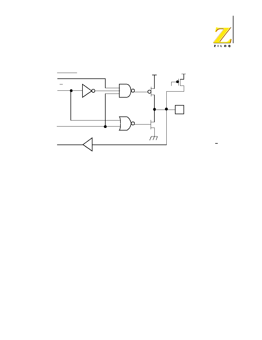
Peripherals
Analog Comparators
The Z86D99/Z86L99 family includes two independent on-chip general-purpose
analog comparators as shown in Figure 13. The comparators are multiplexed with
a digital input signal by the P456CON register. They can also be used to generate
interrupts IRQ0 and IRQ2. The comparators are turned off in STOP mode.
Figure 13. Analog Comparators
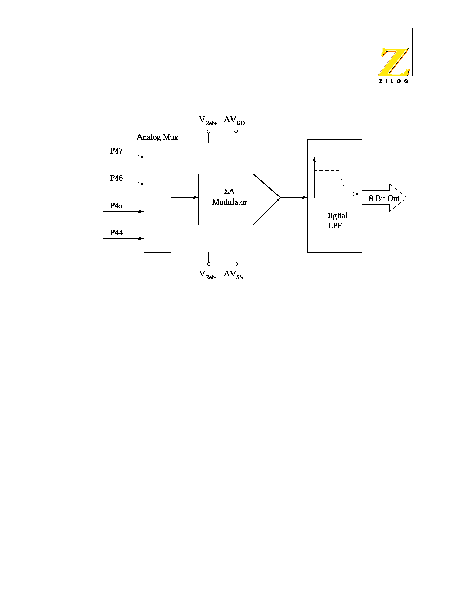
Analog/Digital Converter (ADC)
The Z86D99/Z86L99 family incorporates an 8-bit ADC that uses a sigma delta
architecture (Figure 14) comprised of a modulator and a digital filter. The input is
selected (bit 3,2 from ADCCTRL) with an analog mux from 4 (P47≠P44) pins that
can be configured as analog inputs (bit 7≠4 from ADCCTRL).
Whenever an input pin has an analog value, the digital input
buffer has to be disabled in order to reduce the current through
the device.
+
≠
+
≠
P51
Comparator 1
P50
P52
Comparator 2
P53
P456CON
P456CON
IRQ2, P51 Data Latch
IRQ0, P52 Data Latch
(CIN1)
(CREF1)
(CIN2)
(CREF2)
Bit4 1 = comparator
0 = digital
Bit5 1 = comparator
0 = digital
Note:
Z86D990/Z86D991 OTP and Z86L99X ROM
Low-Voltage Microcontrollers with ADC
PS003807-1002
P R E L I M I N A R Y
29
Figure 14. ADC Block Diagram
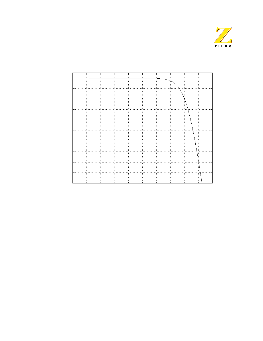
The low-pass filter transfer function is presented in Figure 15 with the ≠3-dB fre-
quency given by the formula:
where f
ADC
is the sampling frequency of the modulator.
f
3db
0.0021 f
ADC
=
Z86D990/Z86D991 OTP and Z86L99X ROM
Low-Voltage Microcontrollers with ADC
PS003807-1002
P R E L I M I N A R Y
30
Figure 15. Low-Pass Filter (with 8-MHz Crystal)
The sampling frequency of the modulator f
ADC
can be selected between f
SCLK
and
f
SCLK
/2 (bit1 from ADCCTRL). Reducing the clock frequency lowers the power
dissipated in the ADC block.
The ADC can be enabled or disabled. When enabled, the
converter tracks the
input voltage. When switching between the channels (step response), the
required time to reach the final value is given by the time constant of the low-pass
filter:
When available, the reference for the ADC is set externally with the V
ref+
and V
ref-
pins. The output code represents the following ratio:
0
0.5
1
1.5
2
2.5
3
3.5
4
4.5
5
20
18
16
14
12
10
8
6
4
2
0
Filter response
log10(f)
Out/In[db]
T
delay
2
f
3db
---------
2
0.0021f
ADC
----------------------------
952
f
ADC
-----------
=
=
=
D
out
V
in
V
Ref-
≠
V
Ref+
V
Ref-
≠
------------------------------- 256
◊
=

Z86D990/Z86D991 OTP and Z86L99X ROM
Low-Voltage Microcontrollers with ADC
PS003807-1002
P R E L I M I N A R Y
31
Though the ADC functions for smaller input voltage range (V
Ref+
≠V
Ref-
), the noise
and offsets remain constant over the specified electrical range. The errors of the
converter increase due to small input signals.
For fast access to the output of the ADC, the current data is available in the ADC
result register (r8, bank00).
To reduce the interference between the digital part and the analog part, separate
AV
SS
and AV
DD
pins are available on the packages where the ADC can be used.
In the smaller packages, which do not support the ADC, the
user must keep the converter not active in order to not have
power dissipated in the ADC block. By default, ADC is off.
Active Glitch Filter
The Z86D99/Z86L99 family incorporates an active power/glitch filter that can be
used to improve the quality of the power supply when the device is operating in
noisy environments. The chips use three separate power buses:
∑
pad ring power bus (all the output drivers plus the crystal/RC oscillator) called
V
DD_padring
∑
core power bus (all digital circuitry) called V
DD_CORE
∑
analog power bus (all analog circuitry) called AV
DD
Depending on the pin availability, one or more of the power buses are connected
together.
The active power filter can be used in the packages that have the V
DD
separate.
Figure 16 shows the internal schematic.
Note:
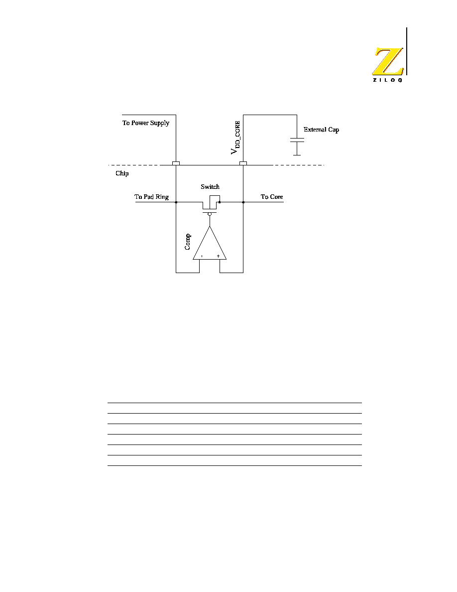
Z86D990/Z86D991 OTP and Z86L99X ROM
Low-Voltage Microcontrollers with ADC
PS003807-1002
P R E L I M I N A R Y
32
Z86D99/Z86L99
Figure 16. Active Glitch/Power Filter
When the internal power/glitch filter is not used, both V
DD_padring
and V
DD_CORE
must be connected together externally to the power supply.
When the internal circuitry is used, the V
DD_padring
has to be connected to the
power supply and the V
DD_CORE
has to be connected to an external energy stor-
age capacitor (1
-10 µ
F range). The core is connected only to this capacitor during
power supply glitches.
Table 8 describes the active glitch/filter specifications.
On the wafer level, all three power buses are available. Depending on the number
of pins of the package, one or more power buses are connected together.
The active glitch/power filter effectively increases the noise immunity for battery-
operated designs where the controller is driving high current loads (for example,
IR LED).
Table 8. Active Glitch/Filter Specifications (Preliminary)
Parameter
Max
Min
Condition
Diff. stage gain
75 dB
Diff. stage bandwidth
15 MHz
Rise time
255 ns
50 mV pulse
Fall time
214 ns
50 mV pulse
R
dson
10
V
DD_padring

Z86D990/Z86D991 OTP and Z86L99X ROM
Low-Voltage Microcontrollers with ADC
PS003807-1002
P R E L I M I N A R Y
33
Controlled Current Output
P43 is an open-drain output-only pin on the Z86D990/D991, but it can be config-
ured as output or Tristate High Impedance on the Z86L990/L991. To function
properly, Bit 3 of P4M must be set to zero to configure the pin as an open-drain
output. For the Z86L990/L991 after reset, P43 defaults to Tristate High Impedance
while the Z86D990/D991 P43 is always configured as output. The data at Port 4
must be initialized as it is undefined at power-on reset.
The current output is a controlled current source that is controlled by the output of
the value of P43 (see Table 9). P43 cannot be configured as input, and if P43 is
read, P43 always returns the state of the output value (1 for no sink and 0 for
sink).
P43 uses internal current reference and will draw current if it outputs a low logic
even without external connection. This applies to both Run mode and Stop mode.
The pad driver can function in two modes:
∑
controlled current output, when the voltage on the pad is over a minimum
value
∑
resistive pull down when the driver cannot regulate the current; in this mode,
the gate of the NMOS pull down is raised to the power rail.
The I-V characteristics of the pad are presented in Figure 17.
Table 9. Current Sink Pad P43 Specifications (Preliminary)
Parameter
Min
Max
Conditions
Rise time
0.4
µ
LED load
Fall time
0.02
µ
LED load
V
outmin
0.54 V
@27C
Comparator response
0.2
µ
Regulated current
80 mA
120 mA
Internal resistance
80
V
pad
V
outmin
>
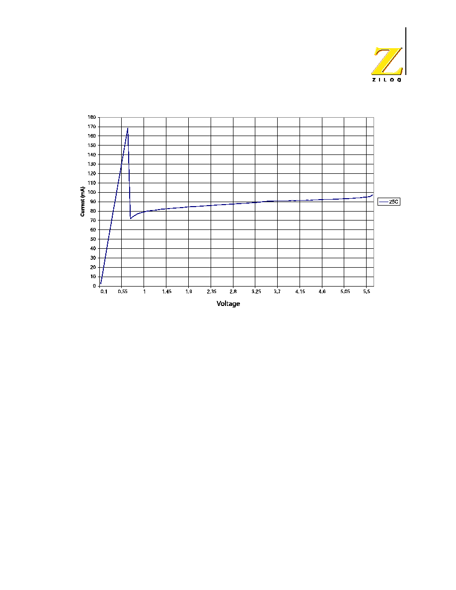
Z86D990/Z86D991 OTP and Z86L99X ROM
Low-Voltage Microcontrollers with ADC
PS003807-1002
P R E L I M I N A R Y
34
Figure 17. I-V Characteristics for the Current Sink Pad P43
The CPU reads the mode of the pad driver by reading bit number 2 from the LB
register. This bit is the output of a Set-Reset flip-flop that sets whenever the volt-
age on the pad is lower than V
outmin
and is reset by a CPU write to the respective
register.
T1 Timer
The Z86D99/Z86L99 family provides one general-purpose 8-bit counter/timer, T
1
,
driven by its own 6-bit prescaler, PRE
1
. The T
1
counter/timer is independent of the
processor instruction sequence, which relieves software from time-critical opera-
tions such as interval timing and event counting.
The T
1
counter/timer operates in either single-pass or continuous mode. At the
end-of-count, counting either stops or the initial value is reloaded and counting
continues. Under software control, new values are loaded immediately or when
the end-of-count is reached. Software also controls the counting mode, how the
counter/timer is started or stopped, and the counter/timer's use of I/O lines. Both
the counter and prescaler registers can be altered while the counter/timer is run-
ning.

Z86D990/Z86D991 OTP and Z86L99X ROM
Low-Voltage Microcontrollers with ADC
PS003807-1002
P R E L I M I N A R Y
35
Counter/timer 1 is driven by a timer clock generated by dividing the internal clock
by four. The divide-by-four stage, the 6-bit prescaler, and the 8-bit counter/timer
form a synchronous 16-bit divide chain. Counter/timer T
1
can also be driven by an
external input (T
IN
) using Port P52. Port P5
6
can serve as a timer output (T
OUT
)
through which T
1
or the internal clock can be output. The timer output toggles at
the end-of-count. Figure 18 is a block diagram of the counter/timer.
Figure 18. T
1
Counter/Timer Block Diagram
OSC
+2
+4
+2
External Clock
Clock
Logic
Internal
Clock
T
IN
P3
1
8-Bit
Down Counter
6-Bit
Down Counter
T1
Initial Value
Register
PRE1
Initial Value
Register
T1
Current Value
Register
Internal Data Bus
T
OUT
P5
6
IRQ5
Internal Clock
Gated Clock
Triggered Clock
Write
Write
Read
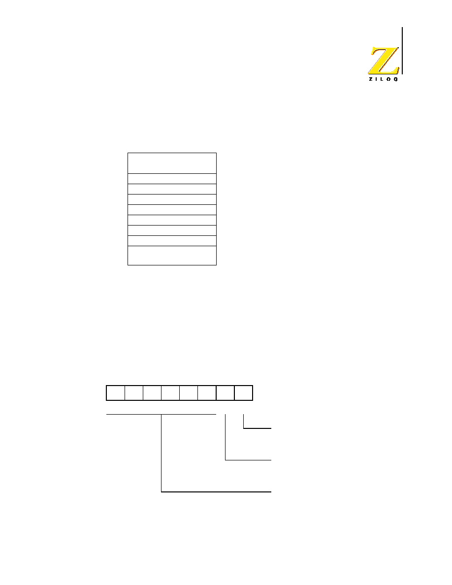
Z86D990/Z86D991 OTP and Z86L99X ROM
Low-Voltage Microcontrollers with ADC
PS003807-1002
P R E L I M I N A R Y
36
The counter/timer, prescaler, and associated mode registers are mapped into the
register file as shown in Figure 19. The software uses the counter/timer as a gen-
eral-purpose register, which eliminates the need for special instructions.
Figure 19. Register File
Prescaler and Counter/Timer
The prescaler PRE
1
(
F3h
) consists of an 8-bit register and a 6-bit down-counter as
shown in Figure 18 on page 35. The prescaler register is a read-write register.
Figure 20 shows the prescaler register.
R243 PRE1
Prescaler 1 Register
(
F3h
; Read/Write)
Figure 20. Prescaler 1 Register
DEC
Hex identifiers
243
T1 prescaler
F3 PRE1
242
Timer/counter 1
F2 T1
241
Timer mode
F1 TMR
D
7
D
6
D
5
D
4
D
3
D
2
D
1
D
0
Count mode
1 = T
1
modulo-N
0 = T
1
single pass
Clock source
1 = T
1
internal
0 = T
1
external (T
IN
)
Prescaler modulo
(range: 1≠64 decimal,
01h
≠
00h
)
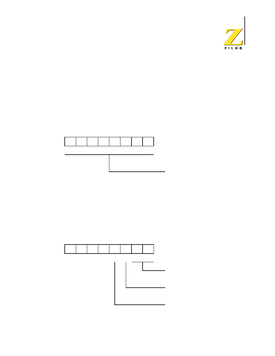
Z86D990/Z86D991 OTP and Z86L99X ROM
Low-Voltage Microcontrollers with ADC
PS003807-1002
P R E L I M I N A R Y
37
The six most significant bits (D
2
≠D
7
) of PRE
1
hold the prescaler count modulo, a
value from 11 to 64 decimal. The prescaler register also contains control bits that
specify T
1
counting modes. These bits also indicate whether the clock source for
T
1
is internal or external.
The counter/timer T
1
(
F2h
) consists of an 8-bit down-counter, a write-only register
that holds the initial count value, and a read-only register that holds the current
count value (see Figure 18 on page 35). The initial value can range from 1 to 256
decimal (
01h
,
02h
, ...,
00h
). Figure 21 illustrates the counter/timer register.
R242 T1
Counter/Timer 1 Register
(
F2h
; Read/Write)
Figure 21. Counter/Timer 1 Register
Counter/Timer Operation
Under software control, T
1
is started and stopped using the Timer Mode register
(
F1h
) bits D
2
≠D
3
: a Load bit and an Enable Count bit. See Figure 22.
R241 TMR
Timer Mode Register
(
F1h
; Read/Write)
Figure 22. Timer Mode Register
D
7
D
6
D
5
D
4
D
3
D
2
D
1
D
0
Initial value when written
(range 1≠256 decimal,
01h
≠
00h
)
Current value when read
D
3
D
2
D
1
D
0
Reserved
0 = No function
1 = Load T
1
0 = Disable T
1
count
1 = Enable T
1
count
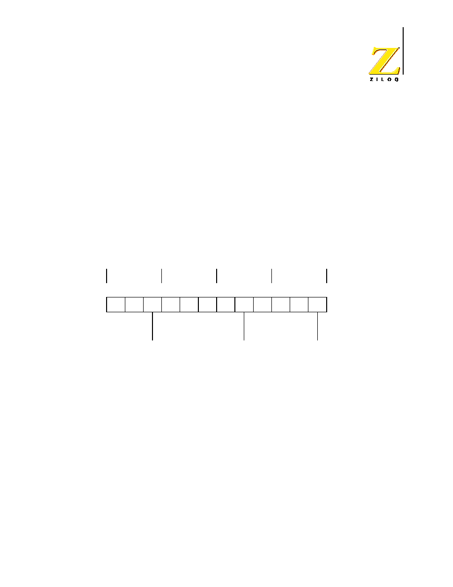
Z86D990/Z86D991 OTP and Z86L99X ROM
Low-Voltage Microcontrollers with ADC
PS003807-1002
P R E L I M I N A R Y
38
Load and Enable Count Bits
Setting the Load bit D
2
to
1
transfers the initial values in the prescaler and the
counter/timer registers into their respective down-counters. The next internal clock
resets bit D
2
to
0
, readying the Load bit for the next load operation. The initial val-
ues can be loaded into the down-counters at any time. If the counter/timer is run-
ning, the counter/timer continues to run and starts the count over with the initial
value. Therefore, the Load bit actually functions as a software re-trigger.
The T
1
counter/timer remains at rest as long as the Enable Count bit D
3
is
0
. To
enable counting, the Enable Count bit D
3
must be set to
1
. Counting actually starts
when the Enable Count bit is written by an instruction. The first decrement occurs
four internal clock periods after the Enable Count bit has been set.
The Load and Enable Count bits can be set at the same time. For example, using
the instruction
OR TMR #%0C
sets both D
2
and D
3
of TMR to
1
. The initial values of
PRE
1
and T
1
are loaded into their respective counters, and the count is started
after the M2T2 machine state after the operand is fetched as shown in Figure 23.
Figure 23. Starting the Count
Prescaler Operations
During counting, the programmed clock source drives the prescaler 6-bit counter.
The counter is counted down from the value specified by bits D
2
≠D
7
of the corre-
sponding prescaler register, PRE
0
or PRE
1
(Figure 24). When the prescaler
counter reaches its end-of-count, the initial value is reloaded and counting contin-
ues. The prescaler never actually reaches zero. For example, if the prescaler is
set to divide by three, the count sequence is as follows:
3-2-1-3-2-1-3-2...
M
3
M
1
M
2
M
n
T
1
T
2
T
3
T
1
T
2
T
3
T
1
T
2
T
3
T
1
T
2
T
3
#03 is fetched
TMR is written;
counter/timers
are loaded
first decrement
occurs four
clocks later
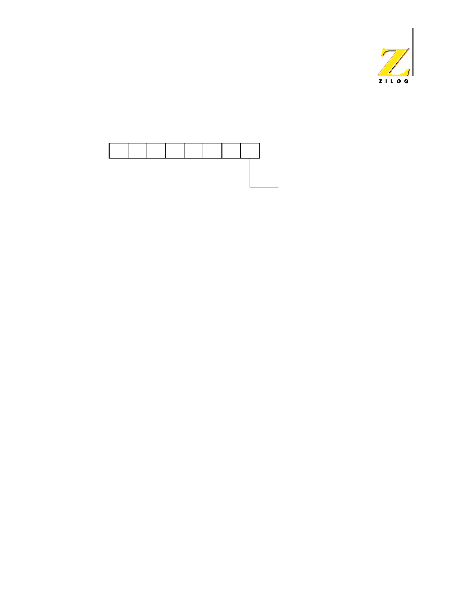
Z86D990/Z86D991 OTP and Z86L99X ROM
Low-Voltage Microcontrollers with ADC
PS003807-1002
P R E L I M I N A R Y
39
R243 PRE1
Prescaler 1 Register
(
F3h
; Read/Write)
Figure 24. Counting Modes
When the PRE
1
register is loaded with 000000 in the six most significant bits, the
prescaler divides by 64. If that number is 000001, the prescaler does not divide
and passes its clock on to T
1
.
Each time the prescaler reaches its end-of-count, a carry is generated, which
allows the counter/timer to decrement by one on the next timer clock input. When
T
1
and PRE
1
both reach their end-of-count, an interrupt request is generated--
IRQ
5
for T
1
. Depending on the counting mode selected, the counter/timer either
comes to rest with its value at
00h
(single-pass mode), or the initial value is auto-
matically reloaded and counting continues (continuous mode). In single-pass
mode, the prescaler still continues to decrement when the timer T
1
has reached
its end-of-count. The prescaler always starts from its programmed value upon
restarting the counter.
The counting modes are controlled by bit D
0
of PRE
1
, with D
0
cleared to
0
for sin-
gle-pass counting mode or set to
1
for continuous mode.
The counter/timer can be stopped at any time by setting the Enable Count bit to
0
and restarted by setting the Enable Count bit back to
1
. The T
1
counter/timer con-
tinues its count value at the time it was stopped. The current value in the T
1
counter/timer can be read at any time without affecting the counting operation.
New initial values can be written to the prescaler or the counter/timer registers at
any time. These values are transferred to their respective down-counters on the
next load operation. If the counter/timer mode is continuous, the next load occurs
on the timer clock following an end-of-count. New initial values must be written
before the load operation because the prescaler always effectively operates in
continuous count mode.
If the value loaded in the T
1
register is
01h
, the timer is actually not timing or
counting at all; the timer is passing the prescaler end-of-count through. Because
the prescaler is continuously running, regardless of the single-pass/continuous
mode operation, the 8-bit timer continuously times out at the rate of the prescaler
end-of-count if the T
1
timer value is programmed to
01h
.
D
0
Count mode
1 = T
1
modulo-N
0 = T
1
single pass
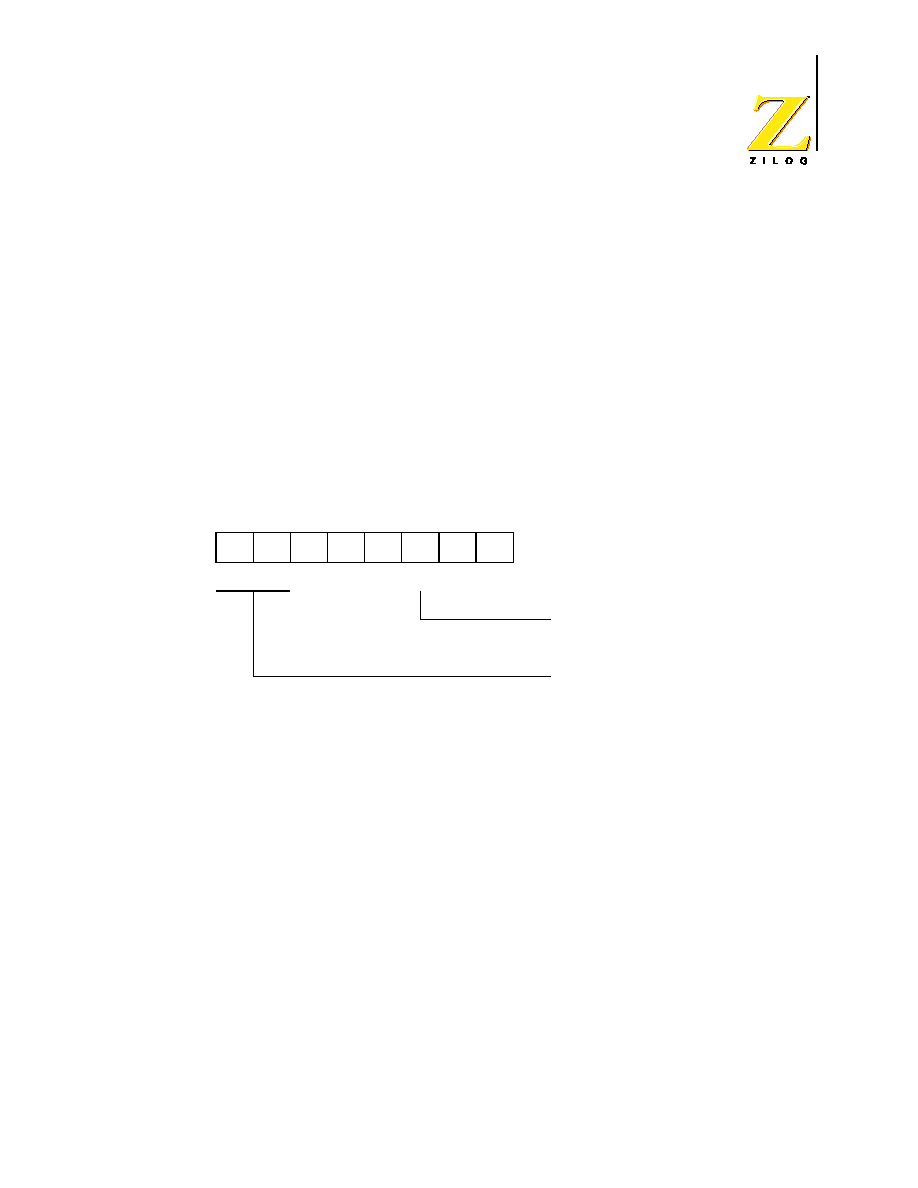
Z86D990/Z86D991 OTP and Z86L99X ROM
Low-Voltage Microcontrollers with ADC
PS003807-1002
P R E L I M I N A R Y
40
The time interval (i) until end-of-count, is given by
i = t x p x v
where t is 8 divided by XTAL frequency, p is the prescaler value (1 ≠ 64), and v is
the counter/timer value (1 ≠ 256). The prescaler and counter/timer are true divide-
by-n counters.
T
OUT
Modes
The Timer Mode register TMR (
F1h
) (Figure 25) is used in conjunction with the
Port 5 Mode register P5M to configure P5
6
for T
OUT
operation. In order for T
OUT
to
function, P5
6
must be defined as an output line by setting P5M bit D
6
to
0
. Output
is controlled by one of the counter/timers (T
0
or T
1
) or the internal clock.
R241 TMR
Timer Mode Register
(
F1h
; Read/Write)
Figure 25. Timer Mode Register T
OUT
Operation
The P5
6
output is selected by TMR bits D
7
and D
6
. T
1
is selected by setting D
7
and D
6
to
1
and
0
, respectively. The counter/timer T
OUT
mode is turned off by set-
ting TMR bits D
7
and D
6
both to
0
, freeing P3
6
to be a data output line.
T
OUT
is initialized to a logic 1 whenever the TMR Load bit D
2
is set to
1
.
At end-of-count, the interrupt request line IRQ
5
clocks a toggle flip-flop. The out-
put of this flip-flop drives the T
OUT
line P5
6
. In all cases, when the counter/timer
reaches its end-of-count, T
OUT
toggles to its opposite state (see Figure 26). If, for
example, the counter/timer is in continuous counting mode, T
OUT
has a 50% duty
cycle output. You can control the duty cycle by varying the initial values after each
end-of-count.
D
7
D
6
D
2
0 = No function
1 = Load T
1
T
OUT
modes
T
OUT
off = 00
Reserved = 01
T
1
out = 10
Internal clock out = 11
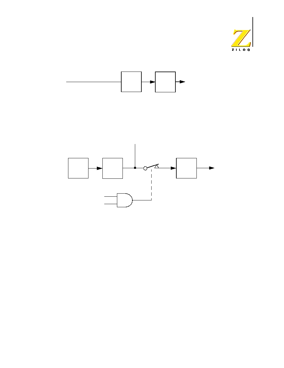
Z86D990/Z86D991 OTP and Z86L99X ROM
Low-Voltage Microcontrollers with ADC
PS003807-1002
P R E L I M I N A R Y
41
Figure 26. Counter/Timer Output Using T
OUT
The internal clock can be selected as output instead of T
1
by setting TMR bits D
7
and D
6
both to
1
. The internal clock (XTAL frequency/2) is then directly output on
P5
6
(Figure 27).
Figure 27. Internal Clock Output Using T
OUT
While programmed as T
OUT
, P5
6
cannot be modified by a write to port register P5.
However, the Z8 software can examine P5
6
's current output by reading the port
register.
T
IN
Modes
The Timer Mode register TMR (
F1h
) (Figure 28) is used in conjunction with the
Prescaler register PRE
1
(
F3h
) (Figure 29) to configure P5
2
as T
IN
. T
IN
is used in
conjunction with T
1
in one of four modes:
∑
External clock input
∑
Gated internal clock
∑
Triggered internal clock
∑
Retriggerable internal clock
+2
P5
6
T
OUT
IRQ5 (T1 end-of-count)
OSC
+2
Internal clock
P5
6
T
OUT
TMR
TMR
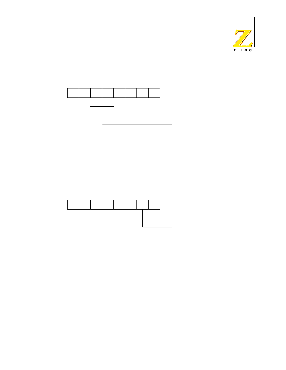
Z86D990/Z86D991 OTP and Z86L99X ROM
Low-Voltage Microcontrollers with ADC
PS003807-1002
P R E L I M I N A R Y
42
R241 TMR
Timer Mode Register
(
F1h
; Read/Write)
Figure 28. Timer Mode Register T
IN
Operation
R243 PRE1
Prescaler 1 Register
(
F3h
; Write Only)
Figure 29. Prescaler 1 T
IN
Operation
The T
1
counter/timer clock source must be configured for external by setting
PRE
1
bit D
2
to
0
. The Timer Mode register bits D
5
and D
4
can then be used to
select the T
IN
operation.
For T
1
to start counting as a result of a T
IN
input, the Enable Count bit D
3
in TMR
must be set to
1
. When using T
IN
as an external clock or a gate input, the initial
values must be loaded into the down-counters by setting the Load bit D
2
in TMR
to
1
before counting begins. Initial values are automatically loaded in Trigger and
Retrigger modes, so software loading is unnecessary.
Configure P5
2
as an input line by setting P5M bit D
2
to
1
.
D
5
D
4
T
IN
modes
External clock input = 00
Gate input = 01
Trigger input = 10
(non-retriggerable)
Trigger input = 11
(retriggerable)
D
1
Clock source
1 = T
1
internal
0 = T
1
external (T
IN
)
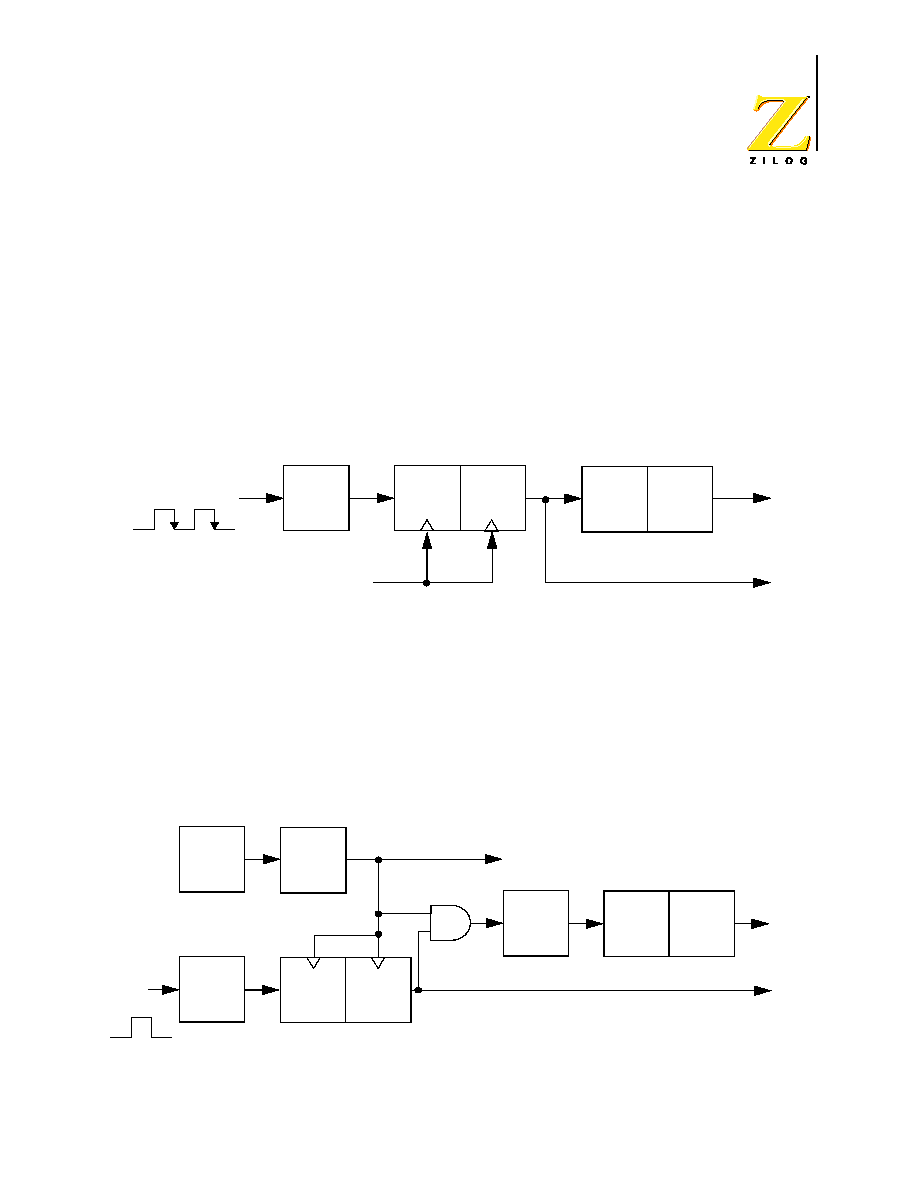
Z86D990/Z86D991 OTP and Z86L99X ROM
Low-Voltage Microcontrollers with ADC
PS003807-1002
P R E L I M I N A R Y
43
Each High-to-Low transition on T
IN
generates interrupt request IRQ
0
, regardless
of the selected T
IN
mode or the enabled/disabled state of T
1
. IRQ
0
must therefore
be masked or enabled according to the needs of the application.
External Clock Input Mode
The T
IN
External Clock Input mode (TMR bits D
5
and D
4
both set to
0
) supports
the counting of external events, where an event is considered to be a High-to-Low
transition on T
IN
(see Figure 30) occurrence (single-pass mode) or on every nth
occurrence (continuous mode) of that event.
Figure 30. External Clock Input Mode
Gated Internal Clock Mode
The T
IN
Gated Internal Clock mode (TMR bits D
5
and D
4
set to
0
and
1
, respec-
tively) measures the duration of an external event. In this mode, the T
1
prescaler
is driven by the internal timer clock, gated by a High level on T
IN
(see Figure 31).
T
1
counts while T
IN
is High and stops counting when T
IN
is Low. Interrupt request
IRQ
0
is generated on the High-to-Low transition of T
IN
, signaling the end of the
gate input. Interrupt request IRQ
5
is generated if T
1
reaches its end-of-count.
Figure 31. Gated Clock Input Mode
P5
2
D
Internal clock
T1
IRQ5
T
IN
clock
D
PRE1
IRQ0
TMR
D
5
≠D
4
= 00
P5
2
D
Internal clock
+2
IRQ5
T
IN
gate
D
OSC
IRQ0
TMR
D
5
≠D
4
= 01
+4
T1
PRE1
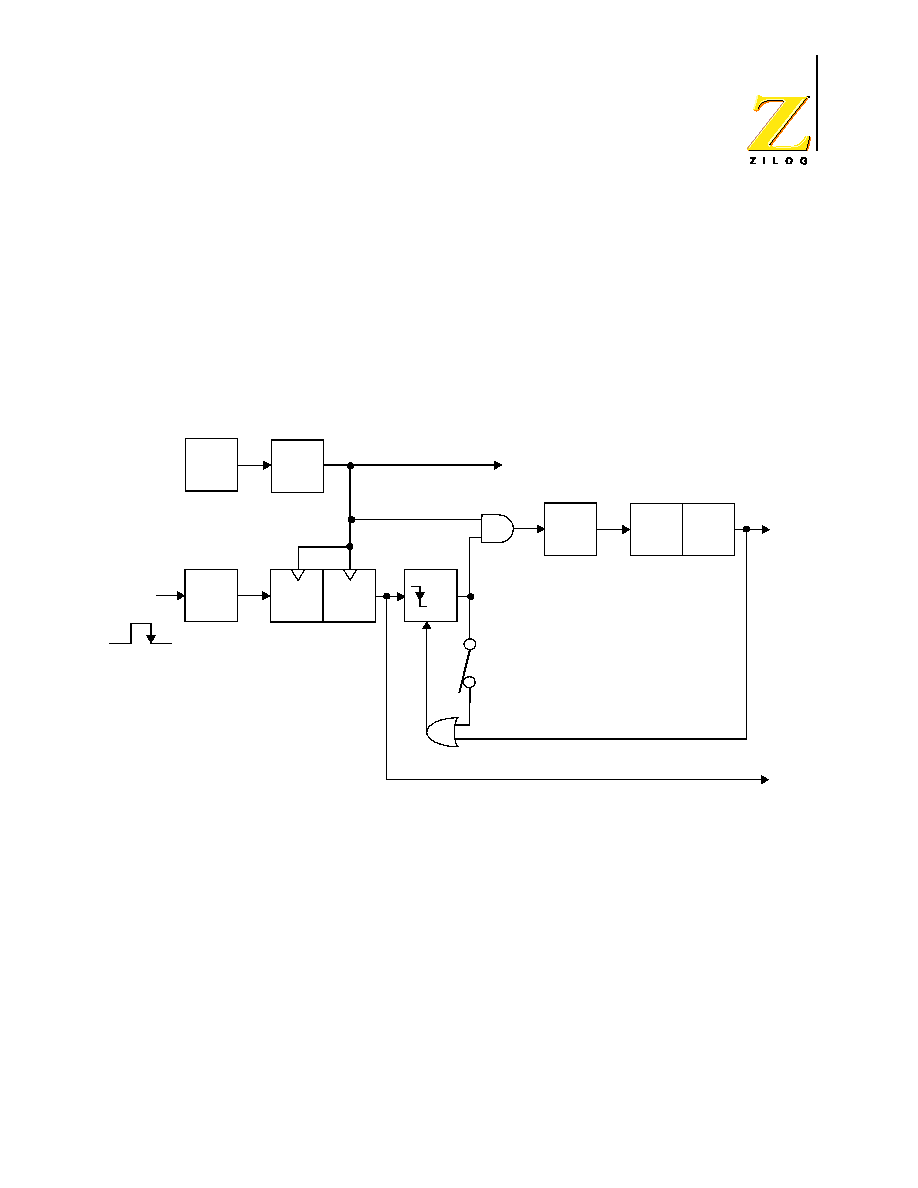
Z86D990/Z86D991 OTP and Z86L99X ROM
Low-Voltage Microcontrollers with ADC
PS003807-1002
P R E L I M I N A R Y
44
Triggered Input Mode
The T
IN
Triggered Input mode (TMR bits D
5
and D
4
set to
1
and
0
, respectively)
causes T
1
to start counting as the result of an external event (see Figure 32). T
1
is
then loaded and clocked by the internal timer clock following the first High-to-Low
transition on the T
IN
input. Subsequent T
IN
transitions do not affect T
1
. In the sin-
gle-pass mode, the Enable bit is reset whenever T
1
reaches its end-of-count. Fur-
ther T
IN
transitions have no effect on T
1
until software sets the Enable Count bit
again. In continuous mode, when T
1
is triggered, counting continues until software
resets the Enable Count bit. Interrupt request IRQ
5
is generated when T
1
reaches
its end-of-count.
Figure 32. Triggered Clock Mode
Retriggerable Input Mode
The T
IN
Retriggerable Input mode (TMR bits D
5
and D
4
both set to
1
) causes T
1
to
load and start counting on every occurrence of a High-to-Low transition on T
IN
(see Figure 32). Interrupt request IRQ
5
is generated if the programmed time inter-
val (determined by T
1
prescaler and counter/timer register initial values) has
elapsed since the last High-to-Low transition on T
IN
. In single-pass mode, the
end-of-count resets the Enable Count bit. Subsequent T
IN
transitions do not
cause T
1
to load and start counting until software sets the Enable Count bit again.
In continuous mode, counting continues when T
1
is triggered until software resets
the Enable Count bit. When enabled, each High-to-Low T
IN
transition causes T
1
to
P5
2
D
Internal clock
+2
IRQ5
T
IN
trigger
D
OSC
IRQ0
TMR
D
5
≠D
4
= 11
+4
T1
PRE1
Edge
trigger
TMR
D
5
= 1

Z86D990/Z86D991 OTP and Z86L99X ROM
Low-Voltage Microcontrollers with ADC
PS003807-1002
P R E L I M I N A R Y
45
reload and restart counting. Interrupt request IRQ
5
is generated on every end-of-
count.
T8 and T16 Timer Operation
The T8 timer is a programmable 8-bit counter/timer with two 8-bit capture regis-
ters and two 8-bit load registers. The T16 timer is a programmable 16-bit counter/
timer with one 16-bit capture register pair and one 16-bit load register pair. See
Figure 33. The T8 and T16 counters/timers have two modes of operation:
∑
The transmit mode is used to generate complex waveforms. There are two
submodes:
≠ The normal mode can be used in single-pass or modulo-N (repeating)
mode.
≠ The ping-pong mode is used when the T8 timer counts down, enables the
T16 timer that counts down, enabling T8, and so on, until the mode is
disabled.
∑
The demodulation mode is used to capture and demodulate complex
waveforms.
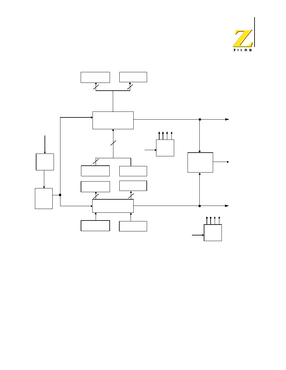
Z86D990/Z86D991 OTP and Z86L99X ROM
Low-Voltage Microcontrollers with ADC
PS003807-1002
P R E L I M I N A R Y
46
Figure 33. Counter/Timer Architecture
T8 Transmit Mode
Before T8 is enabled, the output of T8 depends on CTR1, D1. If CTR1, D1 is 0,
T8_OUT is 1. If CTR1, D1 is 1, T8_OUT is 0.
When T8 is enabled, the output T8_OUT switches to the initial value (CTR1 D1). If
the initial value (CTR1 D1) is 0, TC8L is loaded; otherwise, TC8H is loaded into
the counter. In single-pass mode (CTR0 D6), T8 counts down to 0 and stops,
T8_OUT toggles, the time-out status bit (CTR0 D5) is set, and a time-out interrupt
can be generated if it is enabled (CTR0 D1). In modulo-N mode, upon reaching
terminal count, T8_OUT is toggled, but no interrupt is generated. Then T8 loads a
new count (if T8_OUT level is 0), TC8L is loaded; if T8_OUT is 1, TC8H is loaded.
HI16
16-Bit
T16
8-Bit
T8
Glitch
Filter
Edge
Detect
Circuit
LO16
And/Or
Logic
Timer
8/16
8
8
Timer 16
Timer 8
HI8
LO8
8
8
TC8H
TC8L
8
8
TC16H
TC16L
8
8
16
SCLK
Clock
Divider
T16 Clocked
Input
1 2 4 8
SCLK
Clock
Divider
T8 Clock Divider
1 2 4 8

Z86D990/Z86D991 OTP and Z86L99X ROM
Low-Voltage Microcontrollers with ADC
PS003807-1002
P R E L I M I N A R Y
47
T8 counts down to 0, toggles T8_OUT, sets the time-out status bit (CTR0 D5), and
generates an interrupt if enabled (CTR0 D1). This completes one cycle. T8 then
loads from TC8H or TC8L, according to the T8_OUT level, and repeats the cycle.
The user can modify the values in TC8H or TC8L at any time.The new values take
effect when they are loaded. Do not write these registers at the time the values
are to be loaded into the counter/timer. An initial count of 1 is not allowed. An ini-
tial count of 0 causes TC8 to count from 0 to
FFh
to
FEh
. Transition from 0 to
FFh
is not a time-out condition (see Figure 34).
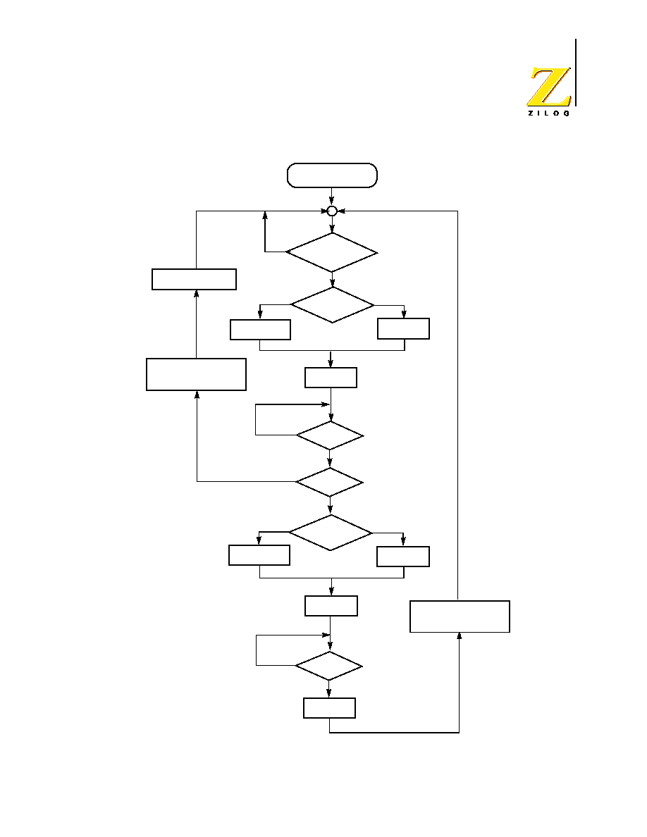
Z86D990/Z86D991 OTP and Z86L99X ROM
Low-Voltage Microcontrollers with ADC
PS003807-1002
P R E L I M I N A R Y
48
Figure 34. Transmit Mode Flowchart
Set Time-out Status Bit
(CTR0 D5) and Generate
Timeout_Int. if Enabled
Set Time-out Status Bit
(CTR0 D5) and Generate
Timeout_Int. if Enabled
T8 (8-Bit)
Transmit Mode
No
T8_Enable Bit Set
CTR0 D7
Yes
CTR1 D1
Value
Reset T8_Enable Bit
0
1
Load TC8L
Reset T8_OUT
Load TC8H
Set T8_OUT
Enable T8
No
T8_Timeout
Yes
Single Pass
Single
Modulo-N
T8_OUT Value
0
Enable T8
No
T8_Timeout
Yes
Disable T8
Pass?
Load TC8H
Set T8_OUT
Load TC8L
Reset T8_OUT
1

Z86D990/Z86D991 OTP and Z86L99X ROM
Low-Voltage Microcontrollers with ADC
PS003807-1002
P R E L I M I N A R Y
49
Do not use the same instructions for stopping the counter/
timers and setting the status bits. Two successive commands
are necessary--the first command for stopping counter/timers
and the second command for resetting the status bits--
because one counter/timer clock interval must complete for the
initiated event to actually occur.
T8 Demodulation Mode
Program TC8L and TC8H to
FFh
. After T8 is enabled, when the first edge (rising,
falling, or both, depending on CTR1 D5, D4) is detected, it starts to count down.
When a subsequent edge (rising, falling, or both, depending on CTR1 D5, D4) is
detected during counting, the current value of T8 is one's complemented and put
into one of the capture registers. If T8 is a positive edge, data is placed in LO8. If
T8 is a negative edge, data is placed in H18. One of the edge-detect status bits
(CTR1 D1, D0) is set, and an interrupt can be generated if enabled (CTR0 D2).
Meanwhile, T8 is loaded with TC8H and starts counting again. If T8 reaches 0, the
time-out status bit (CTR0 D5) is set, and an interrupt can be generated if enabled
(CTR0 D1), and T8 continues counting from
FFh
(see Figure 35).
Note:
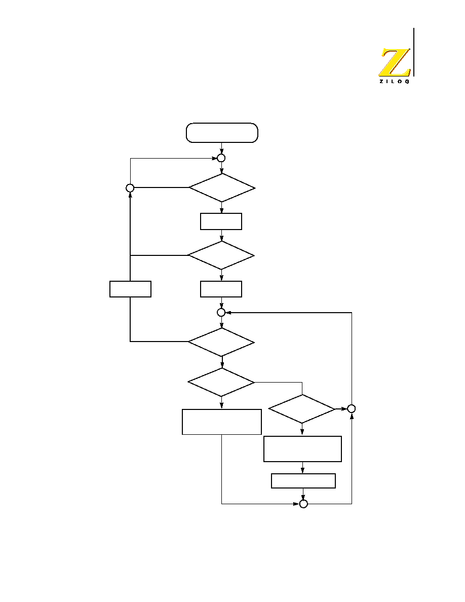
Z86D990/Z86D991 OTP and Z86L99X ROM
Low-Voltage Microcontrollers with ADC
PS003807-1002
P R E L I M I N A R Y
50
Figure 35. Demodulation Mode Flowchart
T8 (8-Bit)
Demodulation Mode
T8 Enable
CTR0, D7
No
Yes
FFh
TC8
First
Edge Present
Enable TC8
T8_Enable
Bit Set
Edge Present
T8 Time Out
Set Edge Present Status
Bit and Trigger Data
Capture Int. if Enabled
Set Time-out Status
Bit and Trigger Time
Out Int. if Enabled
Continue Counting
Disable TC8
No
Yes
No
Yes
Yes
Yes
No
No

Z86D990/Z86D991 OTP and Z86L99X ROM
Low-Voltage Microcontrollers with ADC
PS003807-1002
P R E L I M I N A R Y
51
T16 Transit Mode
In normal or ping-pong mode, the output of T16, when not enabled, is dependent
on CTR1, D0. If CTR1, D0 is a 0, T16_OUT is a 1; if CTR1, D0 is a 1, T16_OUT is
0. The user can force the output of T16 to either a 0 or 1, whether it is enabled or
not, by programming CTR1 D3, D2 to a 10 or 11.
When T16 is enabled, TC16H * 256 + TC16L is loaded, and T16_OUT is switched
to its initial value (CTR1 d0). When T16 counts down to 0, T16_OUT is toggled (in
normal or ping-pong mode), an interrupt is generated if enabled (CTR2 D1), and a
status bit (CTR2 D5) is set. If it is in modulo-N mode, it is loaded with TC16H * 256
+ TC16L, and the counting continues.
The user can modify the values in TC16H and TC16L at any time. The new values
take effect when they are loaded. Do not load these registers at the time the val-
ues are to be loaded into the counter/timer. An initial count of 1 is not allowed. An
initial count of 0 causes T16 to count from 0 to
FFFFh
to
FFFEh
. Transition from 0
to
FFFFh
is not a time-out condition.
T16 Demodulation Mode
Program TC16L and TC16H to
FFh
. After T16 is enabled, when the first edge (ris-
ing, falling, or both, depending on CTR1 D5, D4) is detected, T16 captures HI16
and LO16, reloads, and begins counting.
Ping-Pong Mode
This operation mode is only valid in transmit mode. T8 and T16 must be pro-
grammed in single-pass mode (CTR0 D6, CTR2 D6), and ping-pong mode must
be programmed in CTR1 D3, D2. The user can begin the operation by enabling
either T8 or T16 (CTR0 D7 or CTR2 D7). For example, if T8 is enabled, T8_OUT
is set to this initial value (CTR1 D1). According to T8_OUT's level, TC8H or TC8L
is loaded into T8. After the terminal count is reached, T8 is disabled, and T16 is
enabled. T16_OUT switches to its initial value (CTR1 D0), data from TC16H and
TC16L is loaded, and T16 starts to count. After T16 reaches the terminal count, it
stops. T8 is enabled again, and the whole cycle repeats. Interrupts can be allowed
when T8 or T16 reaches terminal control (CTR0 D1, CTR2 D1). To stop the ping-
pong operation, write 00 to bits D3 and D2 or CTR1.
Enabling ping-pong operation while the counters/timers are
running can cause intermittent counter/timer function. Disable
the counters/timers, then reset the status flags before starting
the ping-pong mode.
Note:

Z86D990/Z86D991 OTP and Z86L99X ROM
Low-Voltage Microcontrollers with ADC
PS003807-1002
P R E L I M I N A R Y
52
Control and Status Registers
The Z86D99/Z86L99 family has 4 I/O port registers, 33 status and control regis-
ters, and 233 general-purpose RAM registers. The I/O port and control registers
are included in the general-purpose register memory to allow any Z8 instruction to
process I/O or control information directly, thus eliminating the requirement for
special I/O or control instructions. The Z8 instruction set permits direct access to
any of these 37 registers. In addition, each of the 233 general-purpose registers
can also function as an accumulator, an address pointer, or an index register.
Registers identified as "Reserved" do not exist or have not been implemented in
this design.
Register Summary
Table 10 through Table 13 summarize the name and location of all registers. The
register-by-register descriptions follow this section.
Table 10. I/O Port Registers (Group 0, Bank 0, Registers 0≠F)
Grp/Bnk Reg
Register Function
Identifier
(
00h
)
rF
General-Purpose RAM Register
GPR
(
00h
)
rE
General-Purpose RAM Register
GPR
(
00h
)
rD
General-Purpose RAM Register
GPR
(
00h
)
rC
General-Purpose RAM Register
GPR
(
00h
)
rB
General-Purpose RAM Register
GPR
(
00h
)
rA
General-Purpose RAM Register
GPR
(
00h
)
r9
General-Purpose RAM Register
GPR
(
00h
)
r8
General-Purpose RAM Register
GPR
(
00h
)
r7
Analog/Digital Converted Data
ADCDATA
(
00h
)
r6
Port 6 Control Register
P6
(
00h
)
r5
Port 5 Control Register
P5
(
00h
)
r4
Port 4 Control Register
P4
(
00h
)
r3
Reserved
(
00h
)
r2
Port 2 Control Register
P2
(
00h
)
r1
Reserved
(
00h
)
r0
Reserved
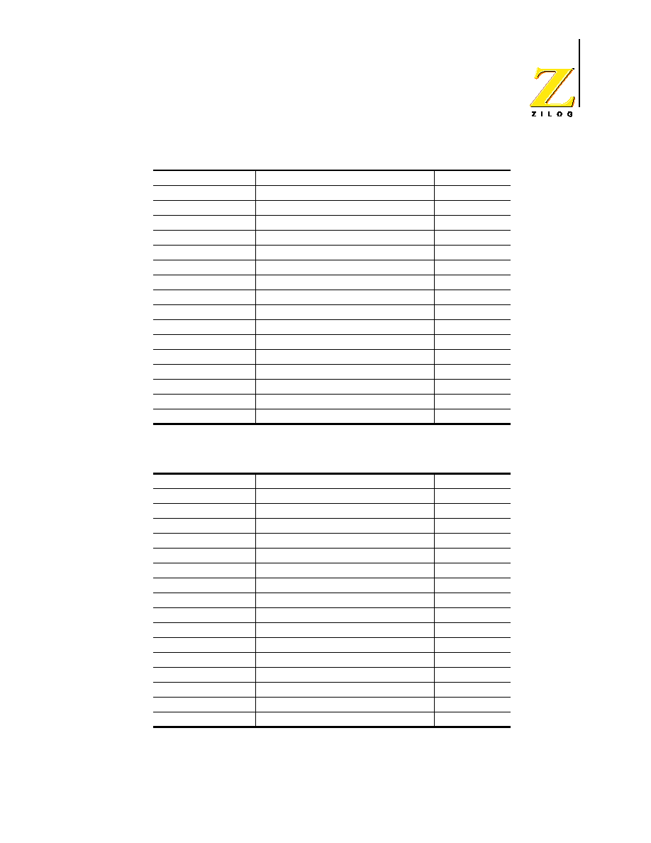
Z86D990/Z86D991 OTP and Z86L99X ROM
Low-Voltage Microcontrollers with ADC
PS003807-1002
P R E L I M I N A R Y
53
Table 11. Control and Status Registers (Group F, Bank 0, Registers 0≠F)
Grp/Bnk Reg
Register Function
Identifier
(
F0h
)
rF
Stack Pointer
SP
(
F0h
)
rE
General-purpose RAM Register
GPR
(
F0h
)
rD
Register Pointer
RP
(
F0h
)
rC
Program Control Flag Register
Flags
(
F0h
)
rB
Interrupt Mask Register
IMR
(
F0h
)
rA
Interrupt Request Register
IRQ
(
F0h
)
r9
Interrupt Priority Register
IPR
(
F0h
)
r8
Reserved
(
F0h
)
r7
Port 3 Mode Register
P3M
(
F0h
)
r6
Port 2 Mode Register
P2M
(
F0h
)
r5
Reserved
(
F0h
)
r4
Reserved
(
F0h
)
r3
T1 Prescale Register
PRE1
(
F0h
)
r2
T1 Data Register
T1
(
F0h
)
r1
T1 Mode Register
TMR
(
F0h
)
r0
Reserved
Table 12. Timer Control Registers (Group 0, Bank D, Registers 0≠F)
Grp/Bnk Reg
Register Function
Identifier
(
0Dh
)
rF
Reserved
(
0Dh
)
rE
Reserved
(
0Dh
)
rD
Reserved
(
0Dh
)
rC
Low-Battery Detect Flag
LB
(
0Dh
)
rB
T16 MS-Byte Capture Register
HI8
(
0Dh
)
rA
T16 LS-Byte Capture Register
LO8
(
0Dh
)
r9
T8 High Capture Register
HI16
(
0Dh
)
r8
T8 Low Capture Register
LO16
(
0Dh
)
r7
T16 MS-Byte Hold Register
TC16H
(
0Dh
)
r6
T16 LS-Byte Hold Register
TC16L
(
0Dh
)
r5
T8 High Hold Register
TC8H
(
0Dh
)
r4
T8 Low Hold Register
TC8L
(
0Dh
)
r3
T8/T16 Control Register B
CTR3
(
0Dh
)
r2
T16 Control Register
CTR2
(
0Dh
)
r1
T8/T16 Control Register A
CTR1
(
0Dh
)
r0
T8 Control Register
CTR0

Z86D990/Z86D991 OTP and Z86L99X ROM
Low-Voltage Microcontrollers with ADC
PS003807-1002
P R E L I M I N A R Y
54
Register Error Conditions
Registers in the Z8 Standard Register File must be used correctly because certain
conditions produce inconsistent results and must be avoided.
∑
Registers
F5h
≠
F9h
are write-only registers. If an attempt is made to read these
registers,
FFh
is returned. Reading any write-only register returns
FFh
.
∑
When the Register Pointer (register FDH) is read, the least significant four bits
(lower nibble) indicate the current Expanded Register File Bank. (For
example, 0000 indicates the Standard Register File, while 1010 indicates
Expanded Register File Bank A.)
∑
Writing to bits that are selected as timer outputs changes the I/O register but
has no effect on the pin signal.
∑
The Z8 instruction DJNZ uses any general-purpose working register as a
counter.
∑
Logical instructions such as OR and AND require that the current contents of
the operand be read. They do not function properly on write-only registers.
Table 13. SMR and Port Mode Registers (Group 0, Bank F, Registers 0≠F)
Grp/Bnk Reg
Register Function
Identifier
(
0Fh
)
rF
Reserved
(
0Fh
)
rE
Reserved
(
0Fh
)
rD
Reserved
(
0Fh
)
rC
Reserved
(
0Fh
)
rB
Stop Mode Recovery Register
SMR
(
0Fh
)
rA
Reserved
(
0Fh
)
r9
Reserved
(
0Fh
)
r8
ADC Control Register
ADCCTRL
(
0Fh
)
r7
Reserved
(
0Fh
)
r6
Port 6 Mode
P6M
(
0Fh
)
r5
Port 5 Stop Mode Recovery
P5SMR
(
0Fh
)
r4
Port 5 Mode Register
P5M
(
0Fh
)
r3
Reserved
(
0Fh
)
r2
Port 4 Mode Register
P4M
(
0Fh
)
r1
Port 2 Stop Mode Recovery
P2SMR
(
0Fh
)
r0
Port Configuration Register
P456CON
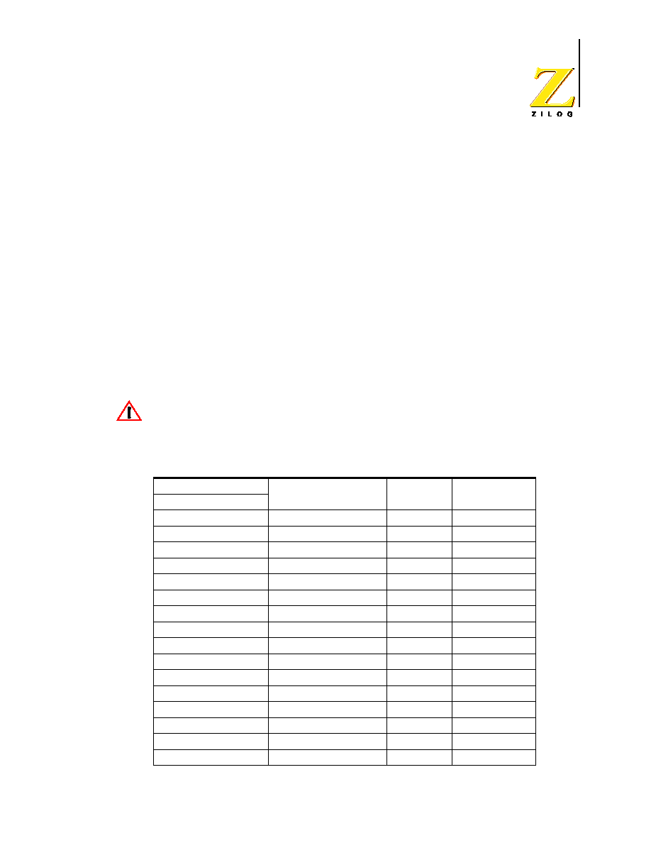
Z86D990/Z86D991 OTP and Z86L99X ROM
Low-Voltage Microcontrollers with ADC
PS003807-1002
P R E L I M I N A R Y
55
Registers (Grouped by Function)
The following is a summary of the 37 special-purpose registers of the Z86D99/
Z86L99 family grouped by function. The following are the functional groups:
∑
Flags and Pointers
∑
Analog-to-Digital Converter Control
∑
Interrupt Control
∑
I/O Port Control
∑
Timer Control--General-Purpose Timer (T1)
∑
Timer Control--T8 and T16 Timers
∑
Stop-Mode Recovery Control
For any of the registers described in this section (see Table 14), bits identified as
"Reserved" either do not exist (meaning they have not been implemented in this
design) or have a special purpose in a ZiLOG engineering or test environment.
Do not attempt to use these bits as the results are
unpredictable and meaningless.
Table 14. Register Description Locations
Address
Grp/Bnk Register
Register Function
Symbol
Location
00h
r2 (R2)
Port 2 Data
P2
page 68
00h
r4 (R4)
Port 4 Data
P4
page 69
00h
r5 (R5)
Port 5 Data
P5
page 70
00h
r6 (R6)
Port 6 Data
P6
page 71
00h
r7 (R7)
ADC Data
ADCDATA
page 62
0Dh
r0
T8 Timer Control
CTR0
page 77
0Dh
r1
T8/T16 Control (A)
CTR1
page 74
0Dh
r2
T16 Timer Control
CTR2
page 80
0Dh
r3
T8/T16 Control (B)
CTR3
page 76
0Dh
r4
T8 Low Load
TC8L
page 79
0Dh
r5
T8 High Load
TC8H
page 79
0Dh
r6
T16 Low Load
TC16L
page 82
0Dh
r7
T16 High Load
TC16H
page 82
0Dh
r8
T16 Low Capture
LO16
page 81
0Dh
r9
T16 High Capture
HI16
page 81
0Dh
r10
T8 Low Capture
LO8
page 78
Caution:
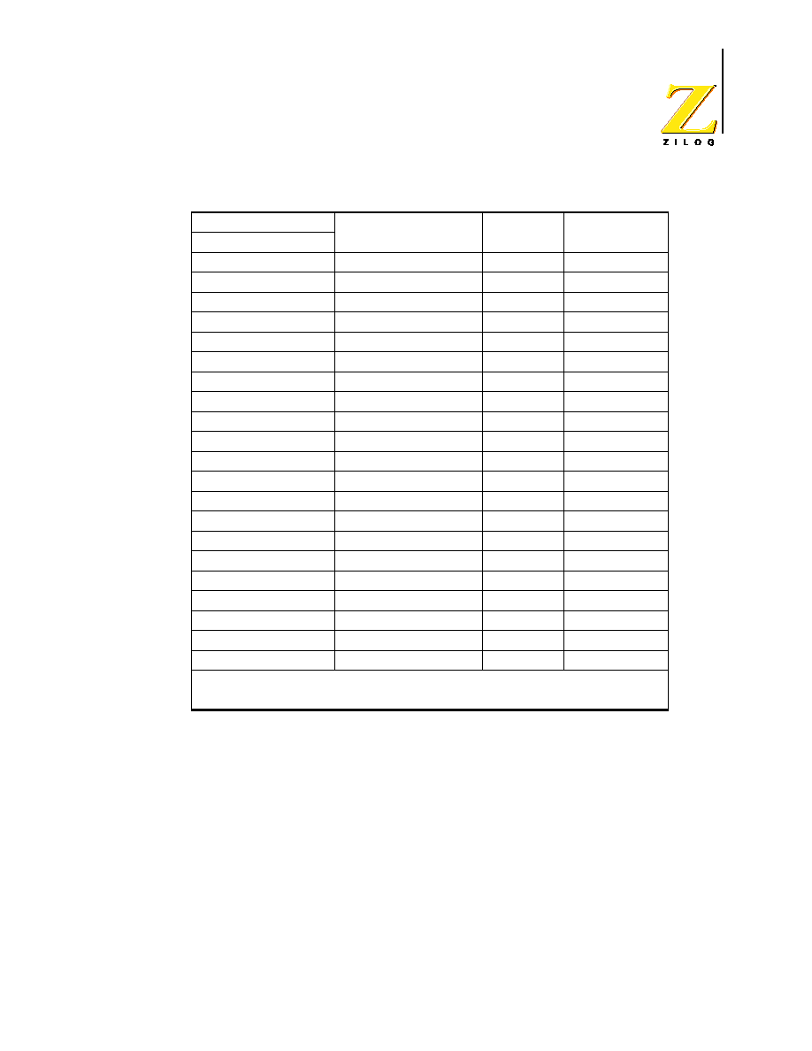
Z86D990/Z86D991 OTP and Z86L99X ROM
Low-Voltage Microcontrollers with ADC
PS003807-1002
P R E L I M I N A R Y
56
Flags and Pointer Registers
In addition to the three standard Z8 flag and pointer registers (Program Control
Register Pointer, and Stack Pointer), the Z86D99/Z86L99 family includes a Low-
Battery Detect Flag register.
0Dh
r11
T8 High Capture
HI8
page 78
0Dh
r12
Low Battery Detect
LB
page 60
0Fh
r0
Port Configuration (A)
P456CON
page 67
0Fh
r1
Port 2 SMR Source
P2SMR
page 84
0Fh
r2
Port 4 Mode
P4M
page 69
0Fh
r4
Port 5 Mode
P5M
page 70
0Fh
r5
Port 5 SMR Source
P5SMR
page 84
0Fh
r6
Port 6 Mode
P6M
page 71
0Fh
r8
ADC Control
ADCCTRL
page 61
0Fh
r11
Stop Mode Recovery
SMR
page 83
F0h
r1 (R241)
T1 Timer Mode
TMR
page 72
F0h
r2 (R242)
T1 Timer Data
T1
page 72
F0h
r3 (R243)
T1 Timer Prescale
PRE1
page 73
F0h
r6 (R246)
Port 2 Mode
P2M
page 68
F0h
r7 (R247)
Port Configuration (B)
P3M
page 67
F0h
r9 (R249)
Interrupt Priority
IPR
page 64
F0h
r10 (R250)
Interrupt Request
IRQ
page 65
F0h
r11 (R251)
Interrupt Mask
IMR
page 63
F0h
r12 (R252)
Program Control Flags Flags
page 57
F0h
r13 (R253)
Register Pointer
RP
page 58
F0h
r15 (R255)
Stack Pointer
SP
page 59
Note:
This register is not reset following Stop Mode Recovery
(SMR).
Table 14. Register Description Locations (Continued)
Address
Grp/Bnk Register
Register Function
Symbol
Location

Z86D990/Z86D991 OTP and Z86L99X ROM
Low-Voltage Microcontrollers with ADC
PS003807-1002
P R E L I M I N A R Y
57
Program Control Flag Register (Flags)
The Program Control Flag register (see Table 15) reflects the current status of the
Z8 as shown in Table 15. The FLAGS register contains six bits of status informa-
tion that are set or cleared by CPU operations. Four of the bits (C, V, Z, and S) can
be tested for use with conditional jump instructions. Two flags (H and D) cannot be
tested and are used for BCD arithmetic. The two remaining flags in the register
(F1 and F2) are available to the user, but they must be set or cleared by instruc-
tions and are not usable with conditional jumps.
Table 15. FLAGS Register [Group/Bank F0h, Register C (R252)]
Bit
7
6
5
4
3
2
1
0
Bit/Field
C
Z
S
V
D
H
F2
F1
R/W
R/W
R/W
R/W
R/W
R/W
R/W
R/W
R/W
Reset
X
X
X
X
X
X
X
X
R = Read, W = Write, X = Indeterminate
Bit
Position
Bit/Field
R/W
Value
Description
7_______
Carry Flag (C)
R/W
1
Indicates the "carry out" of bit 7
position of a register being used as
an accumulator; on Rotate and Shift
instructions this bit contains the most
recent value shifted out of the
specified register
_6______
Zero Flag (Z)
R/W
1
Indicates that the contents of an
accumulator register is zero following
an arithmetic or logical operation
__5_____
Sign Flag (S)
R/W
X
Stores the value of the most
significant bit of a result following an
arithmetic, logical, Rotate, or Shift
operation; in arithmetic operations on
signed numbers, a positive number is
identified by a 0, and a negative
number is identified by a 1
___4____
Overflow
Flag (V)
R/W
1
For signed arithmetic, Rotate, and
Shift operations, the flag is set to 1
when the result is greater than the
maximum possible number (>127) or
less than the minimum possible
number (<-128) that can be
represented in two's complement
form; following logical operations, this
flag is set to 0
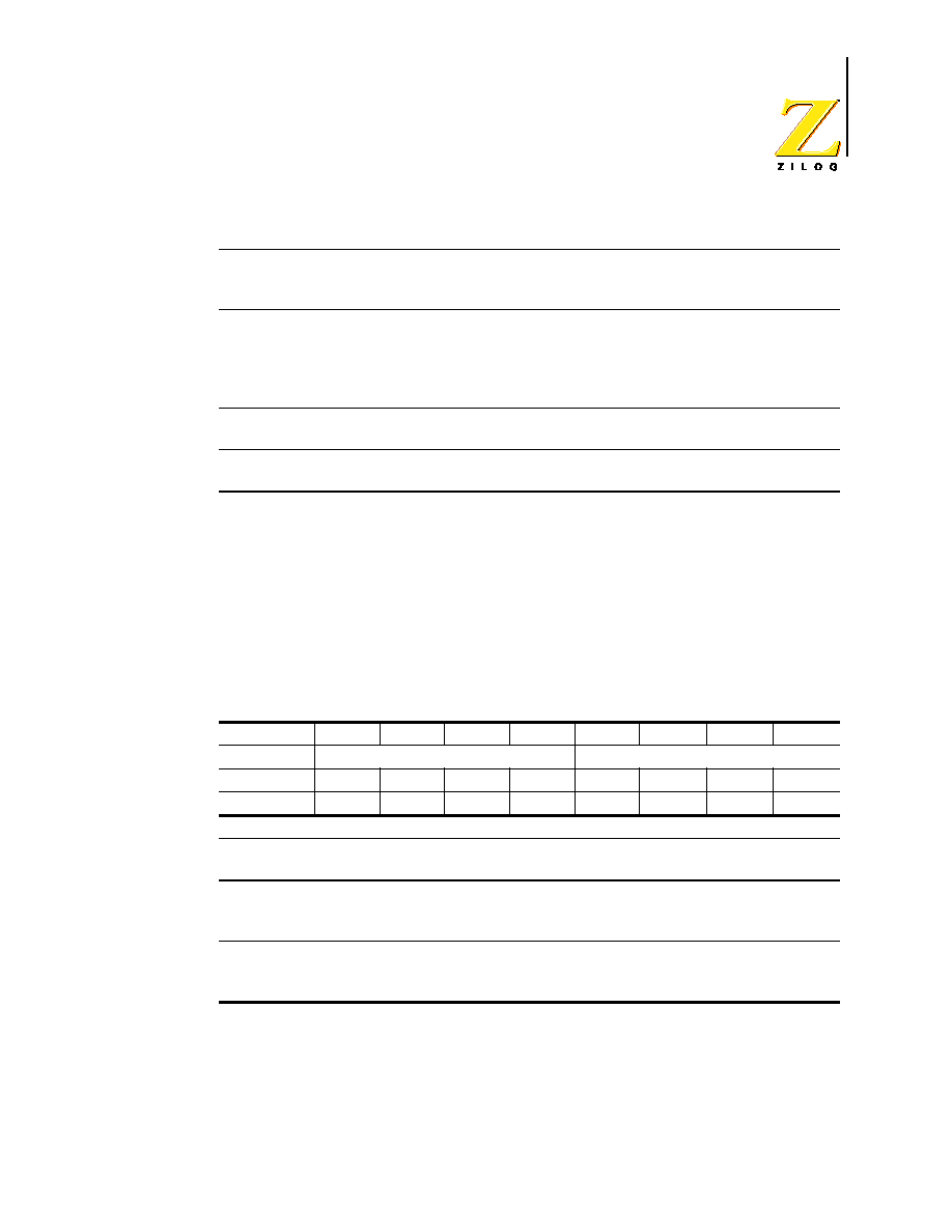
Z86D990/Z86D991 OTP and Z86L99X ROM
Low-Voltage Microcontrollers with ADC
PS003807-1002
P R E L I M I N A R Y
58
Register Pointer (RP)
Z8 instructions can access registers directly or indirectly using either a 4-bit or 8-
bit address field. The upper nibble of the Register Pointer, as described in
Table 16, contains the base address of the active Working Register GROUP. The
lower nibble contains the base address of the Expanded Register File BANK.
When using 4-bit addressing, the 4-bit address of the working register (r0 to rF) is
combined with the upper nibble of the Register Pointer (identifying the WR
GROUP), thus forming the 8-bit actual address.
____3___
Decimal Adjust
Flag (D)
R/W
1
0
Used for BCD arithmetic--after a
subtraction, the flag is set to 1;
following an addition, it is cleared to 0
_____2__
Half Carry
Flag (H)
R/W
1
0
Set to 1, whenever an addition
generates a "carry out" of bit position
3 (overflow) of an accumulator; or
subtraction generates a "borrow into"
bit 3
______1_
User Flag (F2)
R/W
1
0
User definable
_______0
User Flag (F1)
R/W
1
0
User definable
Table 16. RP Register [Group/Bank F0h, Register D (R253)]
Bit
7
6
5
4
3
2
1
0
Bit/Field
Working Register Group
Expanded Register File Bank
R/W
R/W
R/W
R/W
R/W
R/W
R/W
R/W
R/W
Reset
0
0
0
0
0
0
0
0
R = Read, W = Write, X = Indeterminate
Bit
Position
Bit/Field
R/W
Value
Description
7654_____
Working Register
Group Pointer
R/W
X
Identifies 1 of 16 possible WR
Groups, each containing 16 Working
Registers
_____3210
Expanded
Register File
Bank Pointer
R/W
X
Identifies 1 of 16 possible ERF
Banks; only Banks 0, D, and F are
valid for the Z86D99/Z86L99 family
Table 15. FLAGS Register [Group/Bank F0h, Register C (R252)] (Continued)
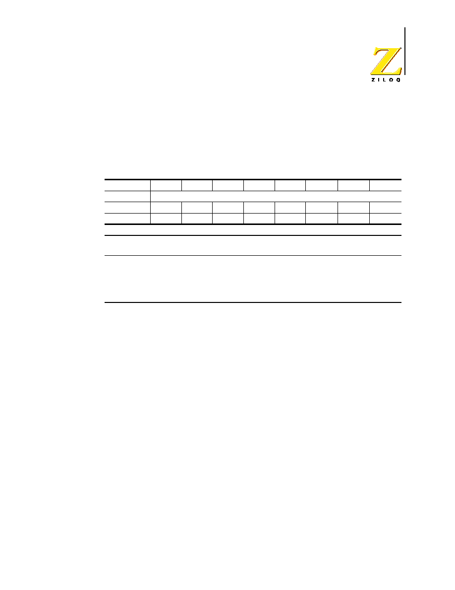
Z86D990/Z86D991 OTP and Z86L99X ROM
Low-Voltage Microcontrollers with ADC
PS003807-1002
P R E L I M I N A R Y
59
Stack Pointer (SP)
The Z86D99/Z86L99 family of products is configured for an internal stack. The
size of the stack is limited only by the available memory space or general-purpose
RAM registers dedicated to this task. An 8-bit stack pointer, as described in
Table 17, is used for all stack operations.
Table 17. SP Register [Group/Bank F0h, Register F (R255)]
Bit
7
6
5
4
3
2
1
0
Bit/Field
Stack Pointer
R/W
R/W
R/W
R/W
R/W
R/W
R/W
R/W
R/W
Reset
X
X
X
X
X
X
X
X
R = Read, W = Write, X = Indeterminate
Bit
Position
Bit/Field
R/W
Value
Description
76543210
Stack Pointer
R/W
X
Points to the data stored on the top of
the stack; an overflow or underflow
can occur if the stack address is
incremented or decremented during
normal stack operations
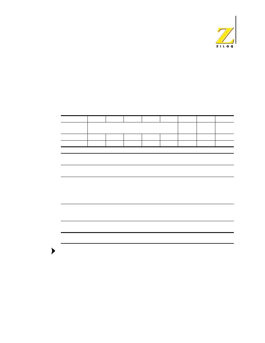
Z86D990/Z86D991 OTP and Z86L99X ROM
Low-Voltage Microcontrollers with ADC
PS003807-1002
P R E L I M I N A R Y
60
Low-Battery Detect Flag (LB)
When the Z86D99/Z86L99 is used in a battery-operated application, one of the
on-chip comparators can be used to check that the V
CC
is at the required level for
correct operation of the device. When voltage begins to approach the V
BO
point,
an on-chip low-battery detection circuit is tripped, which in turn sets a user-read-
able flag. The LB register, as described in Table 18, is used to set and reset the
LB flag.
The LB flag will be valid after enabling the detection for 20
µ
S
(design estimation, not tested in production). LB does not work
at STOP mode. It must be disabled during STOP mode in order
to reduce current.
Table 18. LB Register (Group/Bank 0Dh, Register C)
Bit
7
6
5
4
3
2
1
0
Bit/Field
Reserved
Pad
LVD
LVD_
Flag
LVD_
Enable
R/W
W
W
W
W
W
R/W
R/W
R/W
Reset
1
1
1
1
1
X
0
0
R = Read, W = Write, X = Indeterminate
Bit
Position
Bit/Field
R/W
Value
Description
76543___
Reserved
R
W
1
X
Always reads
11111
No Effect
_____2__
Pad LVD
R
R
W
1
0
X
Pad is not regulated when P43=0
(V
pad
<V
min
; see page 33)
Pad is regulating the current when
P43=0 (V
pad
>V
min
; see page 33)
Reset Pad LB flag
______1_
LVD_Flag
R
R
W
1
0
X
LB Flag Set if
V
DD
<V
LV
LB Flag Reset
No Effect
_______0
LVD_Enable
R/W
1
0
Enable LB *
Disable LB
Note: * When LVD is enabled, IRQ5 is set only for low-voltage detection. Timer 1 will not generate
an interrupt request.
Note:

Z86D990/Z86D991 OTP and Z86L99X ROM
Low-Voltage Microcontrollers with ADC
PS003807-1002
P R E L I M I N A R Y
61
Analog-to-Digital Converter Control Registers
The Z86D99/Z86L99 family features an 8-bit analog-to-digital converter with
external voltage references. The output of the ADC is stored in the ADC Data
Register, as shown in Table 20. The ADC is configured using the ADC Control
Register, as shown in Table 19.
ADC Control Register (ADCCTRL)
The ADCCTRL register controls the operation of the analog-to-digital converter.
Bits 2 and 3 of the ADCCTRL register determine which of the four analog input
channels feeds into the ADC at any given time. Bits 4 through 7 enable or disable
the digital input buffer. When configured as an ADC input channel, the port has to
be configured in Input Mode and with the digital input buffer disabled.
Table 19. ADCCTRL Register (Group/Bank 0Fh, Register 8)
Bit
7
6
5
4
3
2
1
0
Bit/Field
P47_
A/D
P46_
A/D
P45_
A/D
P44_
A/D
Channel
Selection
A/D Pwr
On
ADC
Clock
Select
R/W
R/W
R/W
R/W
R/W
R/W
R/W
R/W
R/W
Reset
0
0
0
0
0
0
0
0
R = Read, W = Write, X = Indeterminate
Bit
Position
Bit/Field
R/W
Value
Description
7_______
P47_A/D
R/W
1
0
P47 configured as A/D Input
P47 configured as digital input
_6______
P46_A/D
R/W
1
0
P46 configured as A/D Input
P46 configured as digital input
__5_____
P45_A/D
R/W
1
0
P45 configured as A/D Input
P45 configured as digital input
___4____
P44_A/D
R/W
1
0
P44 configured as A/D Input
P44 configured as digital input
____32__
Channel
Selection
R/W
11
10
01
00
Channel 3 (P47)
Channel 2 (P46)
Channel 1 (P45)
Channel 0 (P44)
______1_
A/D_PowerON
R/W
1
0
ON
OFF
_______0
ADC Clock Select R/W
1
0
SCLK/2
SCLK
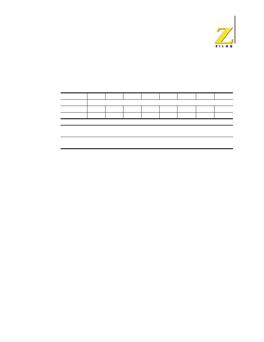
Z86D990/Z86D991 OTP and Z86L99X ROM
Low-Voltage Microcontrollers with ADC
PS003807-1002
P R E L I M I N A R Y
62
ADC Data Register (ADCDATA)
The ADCDATA register is a read-only register that contains the digital output of
the analog-to-digital converter. See Table 20.
)
Interrupt Control Registers
The Z8 allows up to six different interrupts from a variety of sources. These inter-
rupts can be masked and their priorities set by using the Interrupt Mask Register
and Interrupt Priority Register. The Interrupt Request Register stores the interrupt
requests for both vectored and polled interrupts.
Table 20. ADCDATA Register (Group/Bank 00h, Register 7)
Bit
7
6
5
4
3
2
1
0
Bit/Field
ADC Data
R/W
R
R
R
R
R
R
R
R
Reset
0
0
0
0
0
0
0
0
R = Read, W = Write, X = Indeterminate
Bit
Position
Bit/Field
R/W
Value
Description
76543210
ADC Data
R
W
Data
X
Output of the ADC
No Effect

Z86D990/Z86D991 OTP and Z86L99X ROM
Low-Voltage Microcontrollers with ADC
PS003807-1002
P R E L I M I N A R Y
63
Interrupt Mask Register
The IMR, as described in Table 21, individually or globally enables the six interrupt
requests. Bit 7 of the IMR is the master enable and must be set before any of the
individual interrupt requests can be recognized. Bit 7 must be set and reset by the
enable interrupts and disable interrupts instructions only. The IMR is automatically
reset during an interrupt service routine and set following the execution of an
Interrupt Return (IRET) instruction.
Bit 7 must be reset by the DI instruction before the contents of
the Interrupt Mask Register or the Interrupt Priority Register are
changed except in the following situations:
≠ Immediately after a hardware reset
≠ Immediately after executing an interrupt service routine and before IMR bit
7 has been set by any instruction
Table 21. IMR (Group/Bank 0Fh, Register B)
Bit
7
6
5
4
3
2
1
0
Bit/Field
Master
Re-
served IRQ5
IRQ4
IRQ3
IRQ2
IRQ1
IRQ0
R/W
R/W
R/W
R/W
R/W
R/W
R/W
R/W
R/W
Reset
0
0
0
0
0
0
0
0
R = Read, W = Write, X = Indeterminate
Bit
Position
Bit/Field
R/W
Value
Description
7_______
Master
R/W
1
0
Enable Master Interrupt
Disable Master Interrupt
_6______
Reserved
R
W
1
X
Always reads
1
No Effect
__5_____
IRQ
5
R/W
1
0
Enable IRQ
5
Disable IRQ
5
___4____
IRQ
4
R/W
1
0
Enable IRQ
4
Disable IRQ
4
____3___
IRQ
3
R/W
1
0
Enable IRQ
3
Disable IRQ
3
_____2__
IRQ
2
R/W
1
0
Enable IRQ
2
Disable IRQ
2
______1_
IRQ
1
R/W
1
0
Enable IRQ
1
Disable IRQ
1
_______0
IRQ
0
R/W
1
0
Enable IRQ
0
Disable IRQ
0
Note:

Z86D990/Z86D991 OTP and Z86L99X ROM
Low-Voltage Microcontrollers with ADC
PS003807-1002
P R E L I M I N A R Y
64
Interrupt Priority Register (IPR)
The IPR, as described in Table 22, is a write-only register that sets priorities for
the vectored interrupts in order to resolve simultaneous interrupt requests. There
are 48 sequence possibilities for interrupts. The six interrupts, IRQ
0
to IRQ
5
, are
divided into three groups of two interrupt requests each, as follows:
∑
Group A consists of IRQ
3
and IRQ
5
∑
Group B consists of IRQ
0
and IRQ
2
∑
Group C consists of IRQ
1
and IRQ
4
)
Priorities can be set both within and between groups using the IPR. Bits 1, 2, and
5 of the IPR define the priority of individual members within the groups. Bits 0, 3,
and 4 are encoded to define six priority orders between the three groups. Bits 6
and 7 are reserved.
Table 22. IPR (Group/Bank 0Fh, Register 9)
Bit
7
6
5
4
3
2
1
0
Bit/Field
Reserved
Grp A
IRQ3_5 Int_Group
Grp B
IRQ0_2
Grp C
IRQ1_4
Int_
Group
R/W
W
W
W
W
W
W
W
W
Reset
0
0
0
0
0
0
0
0
R = Read, W = Write, X = Indeterminate
Bit
Position
Bit/Field
R/W
Value
Description
76______
Reserved
W
X
No Effect
__5_____
Grp A Priority:
IRQ
3
and IRQ
5
W
1
0
IRQ
3
>IRQ
5
(Group A)
IRQ
5
>IRQ
3
___43__0
Interrupt Group
Priority
W
111
110
101
100
011
010
001
000
Reserved
B>A>C
C>B>A
B>C>A
A>C>B
A>B>C
C>A>B
Reserved
_____2__
Grp B Priority:
IRQ
0
and IRQ
2
W
1
0
IRQ
0
>IRQ
2
(Group B)
IRQ
2
>IRQ
0
______1_
Grp C Priority:
IRQ
1
and IRQ
4
W
1
0
IRQ
4
>IRQ
1
(Group C)
IRQ
1
>IRQ
4

Z86D990/Z86D991 OTP and Z86L99X ROM
Low-Voltage Microcontrollers with ADC
PS003807-1002
P R E L I M I N A R Y
65
Interrupt Request Register
The IRQ, as described in Table 23, is a read/write register that stores the interrupt
requests for both vectored and polled interrupts. When an interrupt request is
made by any of the six interrupts, the corresponding bit in the IRQ is set to 1.
Table 23. IRQ (Group/Bank 0Fh, Register A)
Bit
7
6
5
4
3
2
1
0
Bit/Field
Interrupt Edge
Set
IRQ5
Set
IRQ4
Set
IRQ3
Set
IRQ2
Set
IRQ1
Set
IRQ0
R/W
R/W
R/W
R/W
R/W
R/W
R/W
R/W
R/W
Reset
0
0
0
0
0
0
0
0
R = Read, W = Write, X = Indeterminate
Bit
Position
Bit/Field
R/W
Value
Description
76______
Interrupt Edge
Trigger
R/W
11
10
01
00
P51 Rise/FallingP52 Rise/Falling
P51 Rising P52 Falling
P51 FallingP52 Rising
P51 FallingP52 Falling
__5_____
Set IRQ
5
R
R
W
W
1
0
1
0
IRQ
5
Inactive
IRQ
5
Active
Set IRQ
5
Reset IRQ
5
___4____
Set IRQ
4
R
R
W
W
1
0
1
0
IRQ
4
Inactive
IRQ
4
Active
Set IRQ
4
Reset IRQ
4
____3___
Set IRQ
3
R
R
W
W
1
0
1
0
IRQ
3
Inactive
IRQ
3
Active
Set IRQ
3
Reset IRQ
3
_____2__
Set IRQ
2
R
R
W
W
1
0
1
0
IRQ
2
Inactive
IRQ
2
Active
Set IRQ
2
Reset IRQ
2
______1_
Set IRQ
1
R
R
W
W
1
0
1
0
IRQ
1
Inactive
IRQ
1
Active
Set IRQ
1
Reset IRQ
1
_______0
Set IRQ
0
R
R
W
W
1
0
1
0
IRQ
0
Inactive
IRQ
0
Active
Set IRQ
0
Reset IRQ
0

Z86D990/Z86D991 OTP and Z86L99X ROM
Low-Voltage Microcontrollers with ADC
PS003807-1002
P R E L I M I N A R Y
66
Whenever a power-on reset is executed, the IRQ is reset to
00h
and disabled.
Before the IRQ accepts requests, it must be enabled by executing an enable inter-
rupts instruction.
IRQ is always cleared to
00h
and is in read-only mode until the
first EI instruction that enables the IRQ to be read/write. Setting
the Global Interrupt Enable bit in the Interrupt Mask Register
(IMR bit 7) does not enable the IRQ. Execution of an EI
instruction is required.
For polled processing, IRQ must be initialized by an EI instruction. To properly ini-
tialize the IRQ, the following code is provided:
CLR
IMR
; make sure vectored interrupts are disabled
EI
; enable IRQ, otherwise it is read only
; not necessary, if interrupts were previously
; enabled
DI
; disable interrupt handling
IMR is cleared before the IRQ enabling sequence to ensure no unexpected inter-
rupts occur when EI is executed. This code sequence must be executed before
programming the application required values for IPR and IMR.
I/O Port Control Registers
Each of the four ports (Ports 2, 4, 5, and 6) has an input register, an output regis-
ter, and an associated buffer and control logic. Because there are separate input
and output registers associated with each port, writing bits defined as inputs
stores the data in the output register. This data cannot be read as long as the bits
are defined as inputs. However, if the bits are reconfigured as output, the data
stored in the output register is reflected on the output pins and can then be read.
This mechanism allows the user to initialize the outputs before driving their loads.
Note:

Z86D990/Z86D991 OTP and Z86L99X ROM
Low-Voltage Microcontrollers with ADC
PS003807-1002
P R E L I M I N A R Y
67
Port Configuration Registers (P456CON and P3M)
The port configuration register (described in Table 24) switches the comparator
inputs from digital to analog and allows Ports 4, 5, and/or 6 to be switched from
push/pull active outputs to open drain outputs. In ZiLOG Test Mode, bit 3 of this
register is used to enable the Address Strobe/Data Strobe. Bit 3 is not available in
User Mode.
Port 2 outputs are configured using the P3M Register, shown in Table 25. Bit 0 of
the P3M Register switches Port 2 from push/pull active to open drain outputs. No
other bits in this register are implemented.
Table 24. P456CON Register (Group/Bank 0Fh, Register 0)
Bit
7
6
5
4
3
2
1
0
Bit/Field
Not Used
P51_
Mode
P52_
Mode
Reserved
P6_
Output
P5_
Output
P4_
Output
R/W
R/W
R/W
R/W
R/W
R/W
W
W
W
Reset
0
0
0
0
0
1
1
1
R = Read, W = Write, X = Indeterminate
Bit
Position
Bit/Field
R/W
Value
Description
76______
Not Used
R/W
These bits exist but do not have any
function assigned to them; they are
reserved for future extensions and must
not be used.
__5_____
Comparator 1
Mode
R/W
1
0
Analog (P50, P51 as Inputs)
Digital inputs
___4____
Comparator 2
Mode
R/W
1
0
Analog comparator inputs (P52, P53
configured as Inputs)
Digital inputs
____3___
Reserved
_____2__
Port 6 Output
Configuration
W
1
0
Push-Pull Active
Open Drain Outputs
Always reads back
1
*
______1_
Port 5 Output
Configuration
W
1
0
Push-Pull Active
Open Drain Outputs
Always reads back
1
*
_______0
Port 4 Output
Configuration
W
1
0
Push-Pull Active
Open Drain Outputs
Always reads back
1
*
Note: *Do not use the read-modify-write instructions (for example, OR and AND) with this register.
Bits 0, 1, and 2 always read back 1.
Note:
For Z86L990/L991, P43 can never be configured as push-pull. After any reset, P43 is
configured as tristate high impedance.
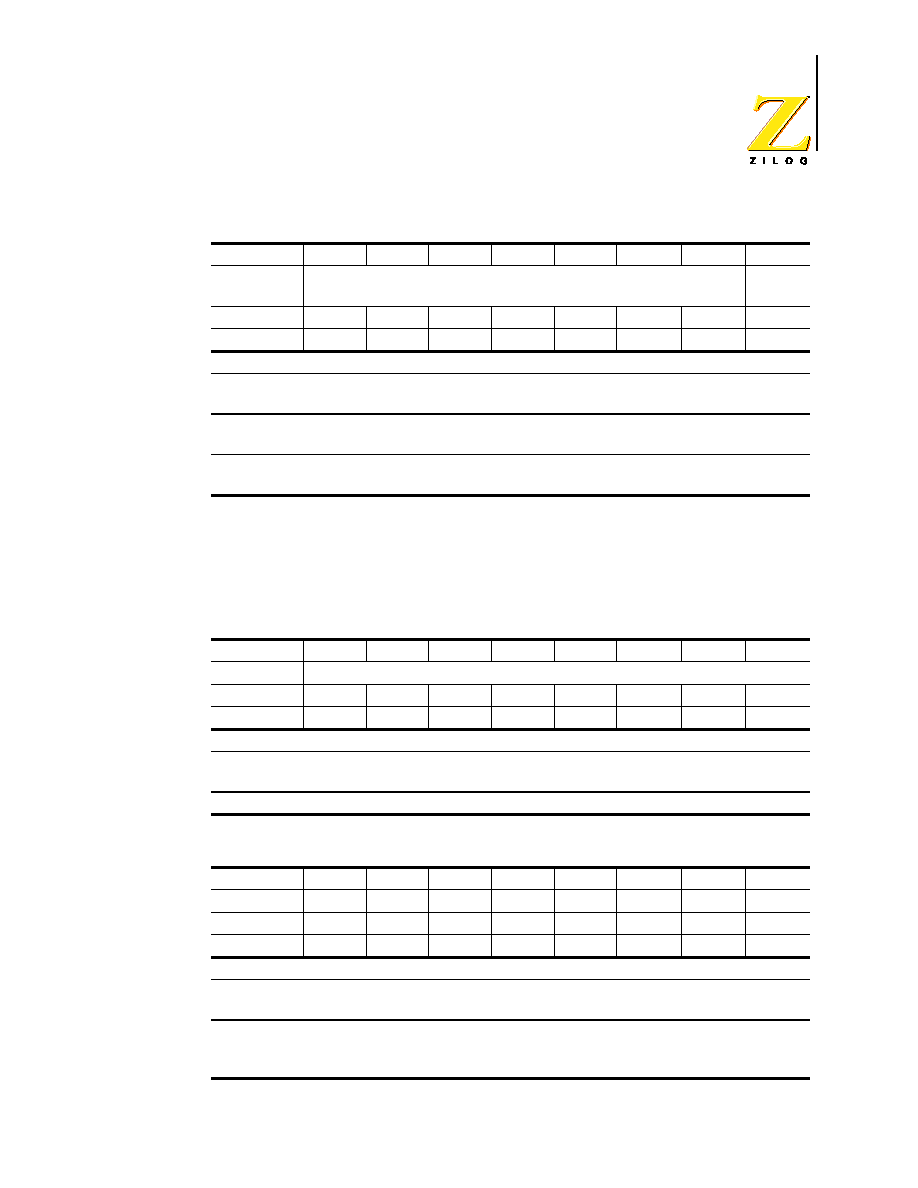
Z86D990/Z86D991 OTP and Z86L99X ROM
Low-Voltage Microcontrollers with ADC
PS003807-1002
P R E L I M I N A R Y
68
Port 2 Control and Mode Registers (P2 and P2M)
Port 2 is a general-purpose 8-bit, bidirectional I/O port, as shown in Table 26.
Each of the eight Port 2 I/O lines can be independently programmed as either
input or output using the Port 2 Mode Register (see Table 27.)
Table 25. P3M Register [Group/Bank F0h, Register 7 (R247)]
Bit
7
6
5
4
3
2
1
0
Bit/Field
Reserved
P2_
Output
R/W
W
W
W
W
W
W
W
W
Reset
1
1
1
1
1
1
1
1
R = Read, W = Write, X = Indeterminate
Bit
Position
Bit/Field
R/W
Value
Description
7654321_
Reserved
R
W
1
X
Always reads
1111111
No Effect
_________0 Port 2 Output
Configuration
W
1
0
Push-Pull Active
Open Drain Outputs
Table 26. P2 Register [Group/Bank 00h, Register 2 (R2)]
Bit
7
6
5
4
3
2
1
0
Bit/Field
Port 2 Data
R/W
R/W
R/W
R/W
R/W
R/W
R/W
R/W
R/W
Reset
X
X
X
X
X
X
X
X
R = Read, W = Write, X = Indeterminate
Bit
Position
Bit/Field
R/W
Value
Description
76543210
Port 2 Data
R/W
Data
Port 2 Input/Output Register
Table 27. P2M Register [Group/Bank F0h, Register 6 (R246)]
Bit
7
6
5
4
3
2
1
0
Bit/Field
P27M
P26M
P25M
P24M
P23M
P22M
P21M
P20M
R/W
W
W
W
W
W
W
W
W
Reset
1
1
1
1
1
1
1
1
R = Read, W = Write, X = Indeterminate
Bit
Position
Bit/Field
R/W
Value
Description
76543210
(by bit)
Port 2 Mode
Select
R
W
W
1
1
0
Always reads
11111111
Input
Output
Z86D990/Z86D991 OTP and Z86L99X ROM
Low-Voltage Microcontrollers with ADC
PS003807-1002
P R E L I M I N A R Y
69
A bit set to 1 in the P2M Register configures the corresponding bit in Port 2 as an
input, while a bit set to 0 configures an output line.
Port 4 Control and Mode Registers (P4 and P4M)
Port 4 is a general-purpose 8-bit, bidirectional I/O port, as shown in Table 28.
Each of the eight Port 4 I/O lines can be independently programmed as either
input or output using the Port 4 Mode Register (see Table 29.)
.
A bit set to 1 in the P4M Register configures the corresponding bit in Port 4 as an
input, while a bit set to 0 configures an output line.
P43, the controlled current output pad, cannot be configured as
an input. (P43 read = P43 out)
Table 28. P4 Register [Group/Bank 00h, Register 4 (R4)]
Bit
7
6
5
4
3
2
1
0
Bit/Field
Port 4 Data
R/W
R/W
R/W
R/W
R/W
R/W
R/W
R/W
R/W
Reset
X
X
X
X
X
X
X
X
R = Read, W = Write, X = Indeterminate
Bit
Position
Bit/Field
R/W
Value
Description
76543210
Port 4 Data
R/W
Data
Port 4 Input/Output Register
Table 29. P4M Register (Group/Bank 0Fh, Register 2)
Bit
7
6
5
4
3
2
1
0
Bit/Field
P47M
P46M
P45M
P44M
P43M
P42M
P41M
P40M
R/W
R/W
R/W
R/W
R/W
R/W
R/W
R/W
R/W
Reset
1
1
1
1
1
1
1
1
R = Read, W = Write, X = Indeterminate
Bit
Position
Bit/Field
R/W
Value
Description
7654_210
(by bit)
Port 4 Mode
Select
R/W
1
0
Input
Output
____3___
P43
Mode Select
R/W
0
1
Output
Tristate High Impedance (available
on Z86L990/L991 only)
Note:
Z86D990/Z86D991 OTP and Z86L99X ROM
Low-Voltage Microcontrollers with ADC
PS003807-1002
P R E L I M I N A R Y
70
Port 5 Control and Mode Registers (P5 and P5M)
Port 5 is a general-purpose 8-bit, bidirectional I/O port, as shown in Table 30.
Each of the eight Port 5 I/O lines can be independently programmed as either
input or output using the Port 5 Mode Register (see Table 31.)
A bit set to a 1 in the P5M Register configures the corresponding bit in Port 5 as
an input, while a bit set to 0 configures an output line.
Regardless of how P5M bits 2 and 3 are set, P52 and P53 are
always in input mode.
Table 30. P5 Register [Group/Bank 00h, Register 5 (R5)]
Bit
7
6
5
4
3
2
1
0
Bit/Field
Port 5 Data
R/W
R/W
R/W
R/W
R/W
R/W
R/W
R/W
R/W
Reset
X
X
X
X
X
X
X
X
R = Read, W = Write, X = Indeterminate
Bit
Position
Bit/Field
R/W
Value
Description
76543210
Port 5 Data
R/W
Data
Port 5 Input/Output Register
Table 31. P5M Register (Group/Bank 0Fh, Register 4)
Bit
7
6
5
4
3
2
1
0
Bit/Field
P57M
P56M
P55M
P54M
P53M
P52M
P51M
P50M
R/W
R/W
R/W
R/W
R/W
R/W
R/W
R/W
R/W
Reset
1
1
1
1
1
1
1
1
R = Read, W = Write, X = Indeterminate
Bit
Position
Bit/Field
R/W
Value
Description
7654__10
(by bit)
Port 5 Mode
Select
R/W
1
0
Input
Output
____32__
P53, P52
Mode Select
R/W
1
Input
Regardless of what is written to this
pin, P53 and P52 are always in input
mode.
Note:
Z86D990/Z86D991 OTP and Z86L99X ROM
Low-Voltage Microcontrollers with ADC
PS003807-1002
P R E L I M I N A R Y
71
Port 6 Control and Mode Registers (P6 and P6M)
Port 6 is a general-purpose 8-bit, bidirectional I/O port, as shown in Table 32.
Each of the eight Port 6 I/O lines can be independently programmed as either
input or output using the Port 6 Mode Register (see Table 33.)
A bit set to 1 in the P6M Register configures the corresponding bit in Port 6 as an
input, while a bit set to 0 configures an output line.
Timer Control Registers--General-Purpose Timer (T1)
The Z86D99/Z86L99 family provides one standard 8-bit Z8 counter/timer, T1,
driven by its own 6-bit prescaler, PRE1. T1 is independent of the processor
instruction sequence, relieving software from time-critical operations such as
interval timing or event counting. There are three registers that control the opera-
tion of T1: T1 Data Register (T1), T1 Mode Register (TMR), and T1 Prescale Reg-
ister (PRE1). Because the timer, prescaler, and mode register are mapped into
the standard Z8 register file, the software can treat the counter/timer as a general-
purpose register, thus eliminating the requirement for special instructions.
Table 32. P6 Register [Group/Bank 00h, Register 6 (R6)]
Bit
7
6
5
4
3
2
1
0
Bit/Field
Port 6 Data
R/W
R/W
R/W
R/W
R/W
R/W
R/W
R/W
R/W
Reset
X
X
X
X
X
X
X
X
R = Read, W = Write, X = Indeterminate
Bit
Position
Bit/Field
R/W
Value
Description
76543210
Port 6 Data
R/W
Data
Port 6 Input/Output Register
Table 33. P6M Register (Group/Bank 0Fh, Register 6)
Bit
7
6
5
4
3
2
1
0
Bit/Field
P67M
P66M
P65M
P64M
P63M
P62M
P61M
P60M
R/W
R/W
R/W
R/W
R/W
R/W
R/W
R/W
R/W
Reset
1
1
1
1
1
1
1
1
R = Read, W = Write, X = Indeterminate
Bit
Position
Bit/Field
R/W
Value
Description
76543210
(by bit)
Port 6 Mode
Select
R/W
1
0
Input
Output
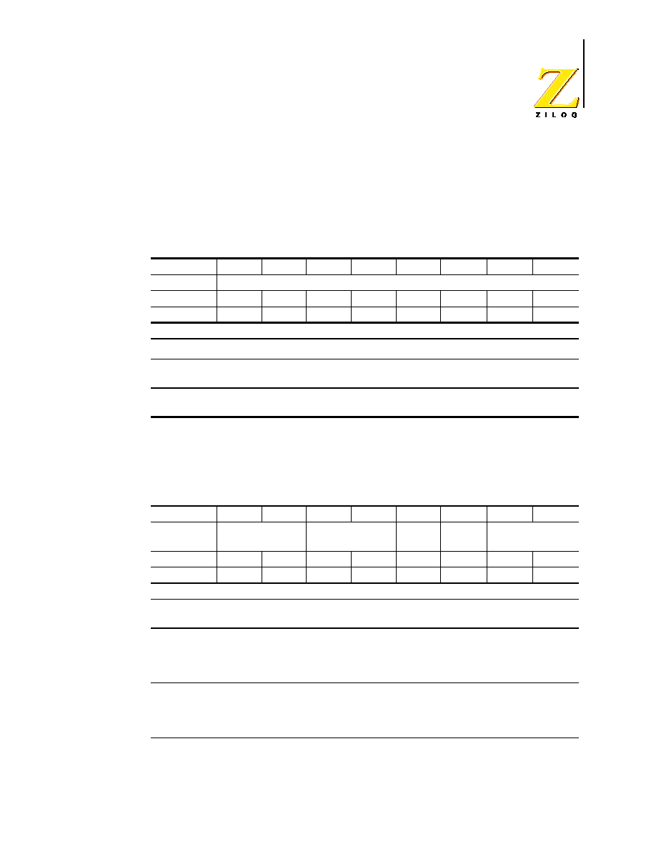
Z86D990/Z86D991 OTP and Z86L99X ROM
Low-Voltage Microcontrollers with ADC
PS003807-1002
P R E L I M I N A R Y
72
T1 Data Register (T1)
The counter/timer register (T1) consists of an 8-bit down counter, a write-only reg-
ister that holds the initial count value, and a read-only register that holds the cur-
rent count value. The initial value of T1 can range from 1 to 255 (0 represents
256) (see Table 34.)
T1 Mode Register (TMR)
Under software control, T1 counter/timer is started and stopped using the T1
Mode Register as shown in Table 35.
Table 34. T1 Register [Group/Bank F0h, Register 2 (R242)]
Bit
7
6
5
4
3
2
1
0
Bit/Field
T1_Value
R/W
R/W
R/W
R/W
R/W
R/W
R/W
R/W
R/W
Reset
0
0
0
0
0
0
0
0
R = Read, W = Write, X = Indeterminate
Bit
Position
Bit/Field
R/W
Value
Description
76543210
T
1
Value
R
W
Data
Data
Current Value
Initial Value (Range 1 to 256 Decimal)
Table 35. TMR Register [Group/Bank F0h, Register 1 (R241)]
Bit
7
6
5
4
3
2
1
0
Bit/Field
TOUT_Mode
TIN_Mode
T1_
Count
T1_
Load
Reserved
R/W
R/W
R/W
R/W
R/W
R/W
R/W
R/W
R/W
Reset
0
0
0
0
0
0
1
1
R = Read, W = Write, X = Indeterminate
Bit
Position
Bit/Field
R/W
Value
Description
76______
T
OUT
Mode
R/W
11
10
01
00
Internal Clock OUT on P56
T
1
OUT on P56
Reserved
Not used (P56 configured as I/O)
__54____
T
IN
Mode
R/W
11
10
01
00
Trigger Input (Retriggerable)
Trigger Input (Not-retriggerable)
Gate Input
External Clock Input (T
IN
on P52)
____3___
T
1
Count
R/W
1
0
Enable T
1
Count
Disable T
1
Count
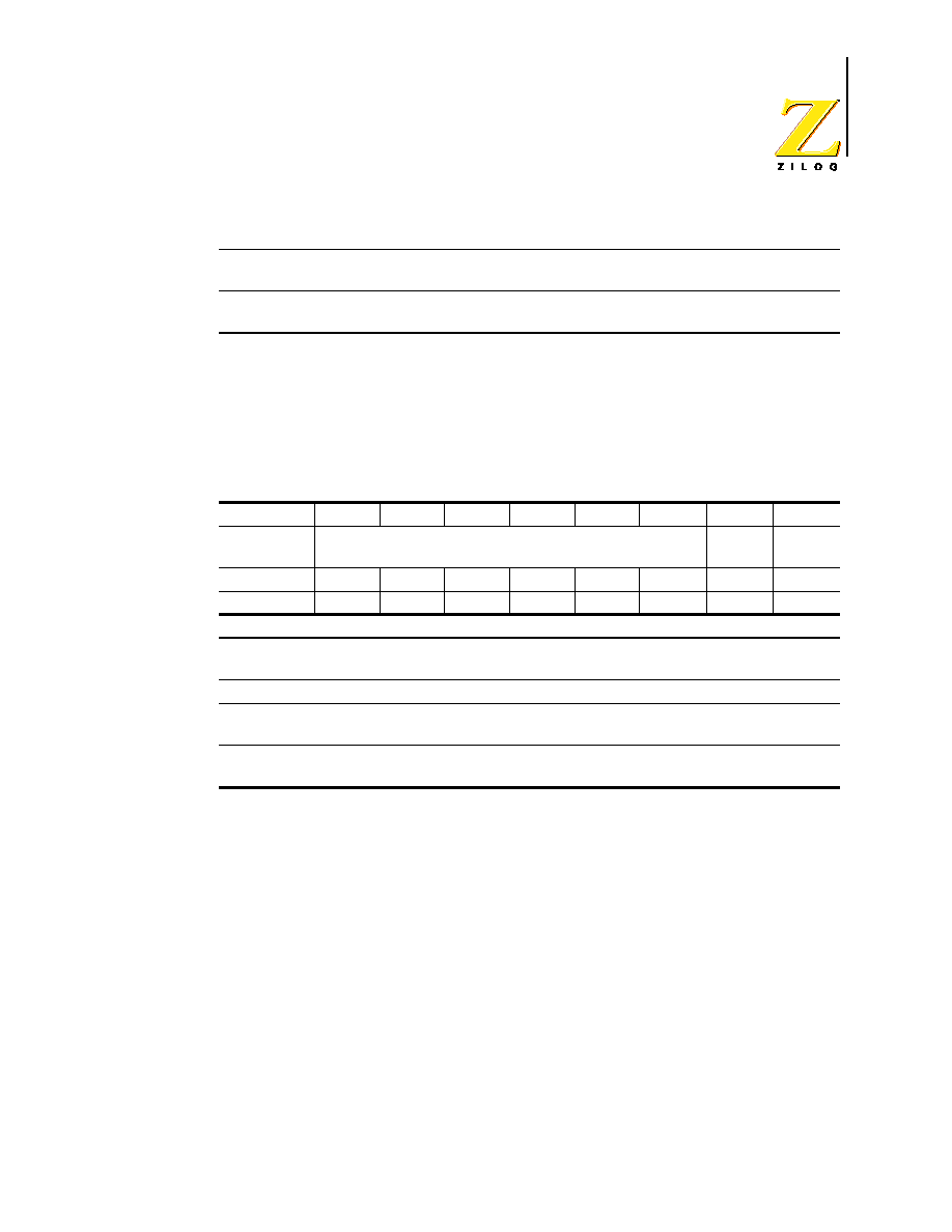
Z86D990/Z86D991 OTP and Z86L99X ROM
Low-Voltage Microcontrollers with ADC
PS003807-1002
P R E L I M I N A R Y
73
T1 Prescale Register (PRE1)
The T1 prescaler consists of an 8-bit register and a 6-bit down-counter. The six
most significant bits (D2≠D7) of PRE1 hold the prescaler's count modulo, a value
from 1 to 64 decimal, as shown in Table 36. The prescale register also contains
control bits that specify the counting mode and clock source for T1.
Timer Control Registers--T8 and T16 Timers
One of the unique features of the Z86D99/Z86L99 family is a special timer archi-
tecture to automate the generation and reception of complex pulses or signals.
This timer architecture consists of one programmable 8-bit counter timer with two
capture registers and two load registers and a programmable 16-bit counter/timer
with one 16-bit capture register pair and one 16-bit load register pair and their
associated control registers. These counter/timers can work independently or can
be combined together using a number of user-selectable modes governed by the
T8/T16 control registers.
_____2__
T
1
Load
R/W
1
0
Load T
1
No effect
______10
Reserved
R
W
1
X
Always reads
11
No effect
Table 36. PRE1 Register [Group/Bank F0h, Register 3 (R243)]
Bit
7
6
5
4
3
2
1
0
Bit/Field
Prescaler_Modulo
Clock_
Source
Count_
Mode
R/W
R/W
R/W
R/W
R/W
R/W
R/W
R/W
R/W
Reset
0
0
0
0
0
0
0
0
R = Read, W = Write, X = Indeterminate
Bit
Position
Bit/Field
R/W
Value
Description
765432__
Prescaler Modulo R/W
Data
Range: 1 to 64 Decimal
_______1_
Clock Source
R/W
1
0
T
1
Internal
T
1
External (T
IN
on P52)
________0
Count Mode
R/W
1
0
T
1
Modulo-n
T
1
Single Pass
Table 35. TMR Register [Group/Bank F0h, Register 1 (R241)] (Continued)

Z86D990/Z86D991 OTP and Z86L99X ROM
Low-Voltage Microcontrollers with ADC
PS003807-1002
P R E L I M I N A R Y
74
T8/T16 Control Register A (CTR1)
The T8/T16 Control Register A controls the functions in common with both the T
8
and T
16
counter/timers. The T
8
and T
16
counter/timers have two primary modes of
operation: Transmit Mode and Demodulation Mode. Transmit Mode is used for
generating complex waveforms. The Transmit Mode has two submodes: Normal
Mode and Ping-Pong Mode. The settings for CTR1 in Transmit Mode are given in
Table 37.
Table 37. CTR1 Register (In Transmit Mode) (Group/Bank 0Dh, Register 1)
Bit
7
6
5
4
3
2
1
0
Bit/Field
Mode
P43
Out
T8/T16_Logic
Transmit_
Submode
Initial_
T8_Out
Initial_
T16_
Out
R/W
R/W
R/W
R/W
R/W
R/W
R/W
R/W
R/W
Reset
0
0
0
0
0
0
0
0
R = Read, W = Write, X = Indeterminate
Bit
Position
Bit/Field
R/W
Value
Description
7_______
Mode
R/W
1
0
Demodulation
Transmit
_6______
P43_Out
R/W
1
0
P43 configured as T8/T16 Output
P43 configured as I/O
__54____
T
8
/T
16
Logic
R/W
11
10
01
00
NAND
NOR
OR
AND
____32__
Transmit_
Submode
R/W
11
10
01
00
T16_Out = 1
T16_Out = 0
Ping-Pong Mode
Normal Operation
______1_
Initial_T8_Out
R/W
1
0
T8_Out set to 1 initially
T8_Out set to 0 initially
_______0
Initial_T16_Out
R/W
1
0
T16_Out set to 1 initially
T16_Out set to 0 initially

Z86D990/Z86D991 OTP and Z86L99X ROM
Low-Voltage Microcontrollers with ADC
PS003807-1002
P R E L I M I N A R Y
75
In Demodulation Mode, the T8 and T16 counter/timers are used to capture and
demodulate complex waveforms. The settings for CTR1 in Demodulation Mode
are given in Table 38.
Table 38. CTR1 Register (in Demodulation Mode) (Group/Bank 0Dh, Register 1)
Bit
7
6
5
4
3
2
1
0
Bit/Field
Mode
Demod
_Input
Edge_Detect
Glitch_Filter
Rising
Edge
Falling
Edge
R/W
R/W
R/W
R/W
R/W
R/W
R/W
R/W
R/W
Reset
0
0
0
0
0
0
0
0
R = Read, W = Write, X = Indeterminate
Bit
Position
Bit/Field
R/W
Value
Description
7_______
Mode
R/W
1
0
Demodulation
Transmit
_6______
Demodulator_
Input
R/W
1
0
P20 as Demodulator Input
P51 as Demodulator Input
__54____
Edge_Detect
R/W
11
10
01
00
Reserved
Both Edges
Rising Edge
Falling Edge
____32__
Glitch_Filter
R/W
11
10
01
00
16 SCLK Cycles
8 SCLK Cycles
4 SCLK Cycles
No Filter
______1_
Rising_Edge
R
R
W
W
1
0
1
0
Rising Edge Detected
No Rising Edge
Reset Flag to 0
No Effect
_______0
Falling_Edge
R
R
W
W
1
0
1
0
Falling Edge Detected
No Falling Edge
Reset Flag to 0
No Effect

Z86D990/Z86D991 OTP and Z86L99X ROM
Low-Voltage Microcontrollers with ADC
PS003807-1002
P R E L I M I N A R Y
76
T8/T16 Control Register B (CTR3)
The T8/T16 Control Register B, known as CTR3, is a new register to the Z86D99/
Z86L99 family. This register allows the T
8
and T
16
counters to be synchronized.
The settings of CTR3 are described in Table 39.
Table 39. CTR3 Register (Group/Bank 0Dh, Register 3)
Bit
7
6
5
4
3
2
1
0
Bit/Field
T16_
Enable
T8_
Enable
Sync
Mode
Reserved
R/W
R/W
R/W
R/W
R/W
R/W
R/W
R/W
R/W
Reset
0
0
0
X
X
X
X
X
R = Read, W = Write, X = Indeterminate
Bit
Position
Bit/Field
R/W
Value
Description
7_______
T
16
Enable
R
R
W
W
1
0
1
0
Counter Enabled
Counter Disabled
Enable Counter
Stop Counter
_6______
T
8
Enable
R
R
W
W
1
0
1
0
Counter Enabled
Counter Disabled
Enable Counter
Stop Counter
__5_____
Sync Mode
R/W
1
0
Enable Sync Mode
Diable Sync Mode
___43210
Reserved
R
W
1
X
Always reads
11111
No Effect

Z86D990/Z86D991 OTP and Z86L99X ROM
Low-Voltage Microcontrollers with ADC
PS003807-1002
P R E L I M I N A R Y
77
T8 Control Register (CTR0)
As shown in Table 40, the T8 Control Register, known as CTR0, controls the oper-
ation of the 8-bit T
8
timer.
Table 40. CTR0 Register (Group/Bank 0Dh, Register 0)
Bit
7
6
5
4
3
2
1
0
Bit/Field
T8_
Enable
Single/
Mod-
ulo-n
Time_
Out
T8_Clock
Capture
INT_
Mask
Counter
INT_
Mask
P40_
Out
R/W
R/W
R/W
R/W
R/W
R/W
R/W
R/W
R/W
Reset
0
0
0
0
0
0
0
0
R = Read, W = Write, X = Indeterminate
Bit
Position
Bit/Field
R/W
Value
Description
7_______
T
8
Enable
R
R
W
W
1
0
1
0
Counter Enabled
Counter Disabled
Enable Counter
Stop Counter
_6______
Single/
Modulo-n
R/W
1
0
Single Pass
Modulo-n
__5_____
Time_Out
R
R
W
W
1
0
1
0
Counter Timeout Occurred
No Counter Timeout
Reset Flag to 0
No Effect
___43___
T
8
Clock
R/W
11
10
01
00
SCLK/8
SCLK/4
SCLK/2
SCLK
_____2__
Capture Interrupt
Mask
R/W
1
0
Enable Data Capture Interrupt
Disable Data Capture Interrupt
______1_
Counter Interrupt
Mask
R/W
1
0
Enable Time_Out Interrupt
Disable Time_Out Interrupt
_______0
P40_Out
R/W
1
0
P40 configured as T
8
Output
P40 configured as I/O
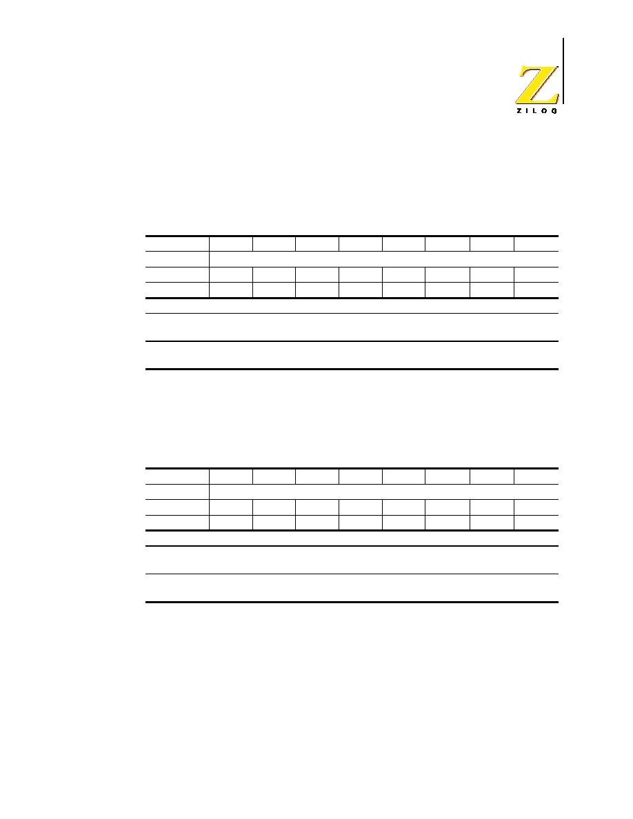
Z86D990/Z86D991 OTP and Z86L99X ROM
Low-Voltage Microcontrollers with ADC
PS003807-1002
P R E L I M I N A R Y
78
T8 High Capture Register (HI8)
The T8 High Capture Register, as described in Table 41, holds the captured data
from the output of the T
8
counter/timer. This register is typically used to hold the
number of counts when the input signal is high (or
1
).
T8 Low Capture Register (LO8)
The T8 Low Capture Register, as described in Table 42, holds the captured data
from the output of the T
8
counter/timer. This register is typically used to hold the
number of counts when the input signal is low (or
0
).
Table 41. HI8 Register (Group/Bank 0Dh, Register B)
Bit
7
6
5
4
3
2
1
0
Bit/Field
T8_Capture_HI
R/W
R/W
R/W
R/W
R/W
R/W
R/W
R/W
R/W
Reset
0
0
0
0
0
0
0
0
R = Read, W = Write, X = Indeterminate
Bit
Position
Bit/Field
R/W
Value
Description
76543210
T
8
Capture
High Value
R
W
Data
Captured Data
No Effect
Table 42. LO8 Register (Group/Bank 0Dh, Register A)
Bit
7
6
5
4
3
2
1
0
Bit/Field
T8_Capture_LO
R/W
R/W
R/W
R/W
R/W
R/W
R/W
R/W
R/W
Reset
0
0
0
0
0
0
0
0
R = Read, W = Write, X = Indeterminate
Bit
Position
Bit/Field
R/W
Value
Description
76543210
T
8
Capture
Low Value
R
W
Data
Captured Data
No Effect
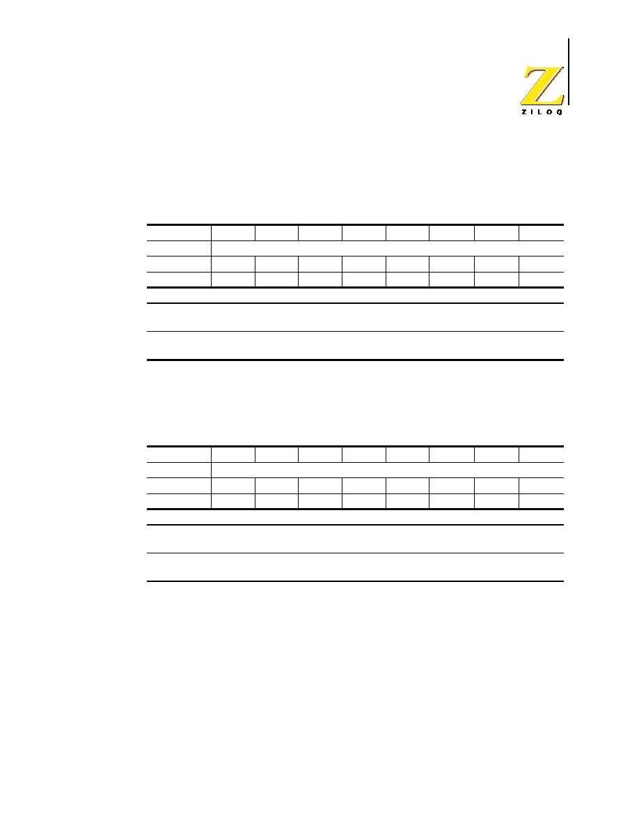
Z86D990/Z86D991 OTP and Z86L99X ROM
Low-Voltage Microcontrollers with ADC
PS003807-1002
P R E L I M I N A R Y
79
T8 High Load Register (TC8H)
The T8 High Load Register, as described in Table 43, is loaded with the counter
value necessary to keep the T8_Out signal in the high state for the required time.
T8 Low Load Register (TC8L)
The T8 Low Load Register, as described in Table 44, is loaded with the counter
value necessary to keep the T8_Out signal in the low state for the required time.
Table 43. TC8H Register (Group/Bank 0Dh, Register 5)
Bit
7
6
5
4
3
2
1
0
Bit/Field
T8_Level_HI
R/W
R/W
R/W
R/W
R/W
R/W
R/W
R/W
R/W
Reset
0
0
0
0
0
0
0
0
R = Read, W = Write, X = Indeterminate
Bit
Position
Bit/Field
R/W
Value
Description
76543210
T
8
Level
High Value
R/W
Data
Duration that T8_Out remains High
Table 44. TC8L Register (Group/Bank 0Dh, Register 4)
Bit
7
6
5
4
3
2
1
0
Bit/Field
T8_Level_LO
R/W
R/W
R/W
R/W
R/W
R/W
R/W
R/W
R/W
Reset
0
0
0
0
0
0
0
0
R = Read, W = Write, X = Indeterminate
Bit
Position
Bit/Field
R/W
Value
Description
76543210
T
8
Level
Low Value
R/W
Data
Duration that T8_Out remains Low

Z86D990/Z86D991 OTP and Z86L99X ROM
Low-Voltage Microcontrollers with ADC
PS003807-1002
P R E L I M I N A R Y
80
T16 Control Register (CTR2)
The T16 Control Register, known as CTR2, controls the operation of the 16-bit T
16
timer (see Table 45).
Table 45. CTR2 Register (Group/Bank 0Dh, Register 2)
Bit
7
6
5
4
3
2
1
0
Bit/Field
T16_
Enable
Single/
Mod-
ulo-n
Time_
Out
T16_Clock
Capture
INT_
Mask
Counter
INT_
Mask
P41_
Out
R/W
R/W
R/W
R/W
R/W
R/W
R/W
R/W
R/W
Reset
0
0
0
0
0
0
0
0
R = Read, W = Write, X = Indeterminate
Bit
Position
Bit/Field
R/W
Value
Description
7_______
T
16
Enable
R
R
W
W
1
0
1
0
Counter Enabled
Counter Disabled
Enable Counter
Stop Counter
_6______
Single/
Modulo-n
R/W
1
0
1
0
In Transmit Mode:
Single Pass
Modulo-n
In Demodulation Mode:
T
16
Does Not Recognize Edge
T
16
Recognizes Edge
__5_____
Time_Out
R
R
W
W
1
0
1
0
Counter Timeout Occurred
No Counter Timeout
Reset Flag to 0
No Effect
___43___
T
16
Clock
R/W
11
10
01
00
SCLK/8
SCLK/4
SCLK/2
SCLK
_____2__
Capture Interrupt
Mask
R/W
1
0
Enable Data Capture Interrupt
Disable Data Capture Interrupt
______1_
Counter Interrupt
Mask
R/W
1
0
Enable Time_Out Interrupt
Disable Time_Out Interrupt
_______0
P41_Out
R/W
1
0
P41 configured as T
16
Output
P41 configured as I/O

Z86D990/Z86D991 OTP and Z86L99X ROM
Low-Voltage Microcontrollers with ADC
PS003807-1002
P R E L I M I N A R Y
81
T16 MS-Byte Capture Register (HI16)
The T16 MS-Byte Capture Register, as described in Table 46, holds the captured
data from the output of the T
16
counter/timer. This register holds the most signifi-
cant byte of the data.
T16 LS-Byte Capture Register (LO16)
The T16 LS-Byte Capture Register, as described in Table 47, holds the captured
data from the output of the T
16
counter/timer. This register holds the least signifi-
cant byte of the data.
Table 46. HI16 Register (Group/Bank 0Dh, Register 9)
Bit
7
6
5
4
3
2
1
0
Bit/Field
T16_Capture_HI
R/W
R/W
R/W
R/W
R/W
R/W
R/W
R/W
R/W
Reset
0
0
0
0
0
0
0
0
R = Read, W = Write, X = Indeterminate
Bit
Position
Bit/Field
R/W
Value
Description
76543210
T
16
Capture HI
R
W
Data
MS-Byte of Captured Data
No Effect
Table 47. LO16 Register (Group/Bank 0Dh, Register 8)
Bit
7
6
5
4
3
2
1
0
Bit/Field
T16_Capture_LO
R/W
R/W
R/W
R/W
R/W
R/W
R/W
R/W
R/W
Reset
0
0
0
0
0
0
0
0
R = Read, W = Write, X = Indeterminate
Bit
Position
Bit/Field
R/W
Value
Description
76543210
T
16
Capture LO
R
W
Data
LS-Byte of Captured Data
No Effect
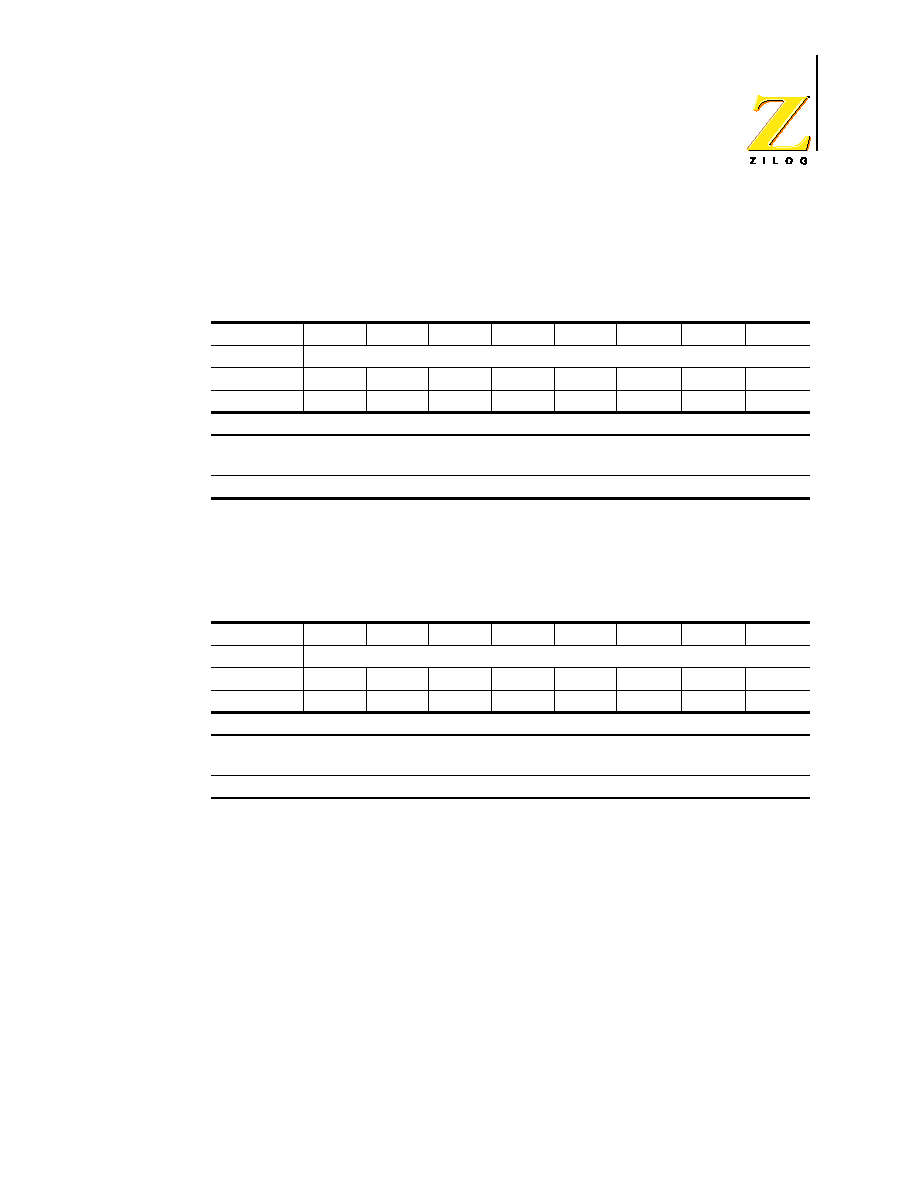
Z86D990/Z86D991 OTP and Z86L99X ROM
Low-Voltage Microcontrollers with ADC
PS003807-1002
P R E L I M I N A R Y
82
T16 MS-Byte Load Register (TC16H)
The T16 MS-Byte Load Register, as described in Table 48, is loaded with the most
significant byte of the T
16
counter value.
T16 LS-Byte Load Register (TC16L)
The T16 LS-Byte Load Register, as described in Table 49, is loaded with the least
significant byte of the T
16
counter value.
Stop-Mode Recovery Control Registers
The Z86D99/Z86L99 family of products allows 16 individual I/O pins (Ports 2 and
5) to be used as a stop-mode recovery sources. The STOP mode is exited when
one of these SMR sources is toggled.
Table 48. TC16H Register (Group/Bank 0Dh, Register 7)
Bit
7
6
5
4
3
2
1
0
Bit/Field
T16_Data_HI
R/W
R/W
R/W
R/W
R/W
R/W
R/W
R/W
R/W
Reset
0
0
0
0
0
0
0
0
R = Read, W = Write, X = Indeterminate
Bit
Position
Bit/Field
R/W
Value
Description
76543210
T
16
Data HI
R/W
Data
MS-Byte of the T
16
Counter
Table 49. TC16L Register (Group/Bank 0Dh, Register 6)
Bit
7
6
5
4
3
2
1
0
Bit/Field
T16_Data_LO
R/W
R/W
R/W
R/W
R/W
R/W
R/W
R/W
R/W
Reset
0
0
0
0
0
0
0
0
R = Read, W = Write, X = Indeterminate
Bit
Position
Bit/Field
R/W
Value
Description
76543210
T
16
Data LO
R/W
Data
LS-Byte of the T
16
Counter

Z86D990/Z86D991 OTP and Z86L99X ROM
Low-Voltage Microcontrollers with ADC
PS003807-1002
P R E L I M I N A R Y
83
Stop-Mode Recovery Register
The SMR register serves two functions. Bit D7 of the SMR register, as shown in
Table 50, is the Stop Mode Flag that is set upon entering stop mode. A 0 in this bit
indicates that the device has been reset by a POR or WDT Reset. A POR or WDT
Reset is sometimes referred to as a "cold" start. A 1 in bit D7 indicates that the
device was awakened by a SMR source. Waking a device with a SMR source is
sometimes referred to as a "warm" start.
The Stop Mode Recovery source can be selected by any combination of P2 and
P5 by P2SMR and P5SMR, respectively. If the pin is selected as the SMR source,
its logic level is latched into a register. A wait up signal is generated if its logic level
changes. This applies to all selected pins for the SMR source.
The comparators of P5 cannot be used as an SMR source. The comparator is
turned off in STOP mode.
The second function of the SMR register is the selection of the external clock
divide value. The purpose of this control is to selectively reduce device power
Table 50. SMR Register (Group/Bank 0Fh, Register B)
Bit
7
6
5
4
3
2
1
0
Bit/Field
Stop
Flag
Re-
served
Stop
Delay
Reserved
SCLK Select
R/W
R
R/W
W
R/W
R/W
R/W
W
W
Reset
0
0
1
0
0
0
0
0
R = Read, W = Write, X = Indeterminate
Bit
Position
Bit/Field
R/W
Value
Description
7_______
Stop Mode Flag
R
R
W
1
0
X
Stop Recovery (warm start)
POR/WDT Reset (cold start)
No Effect
_6______
Reserved
R
W
1
X
Always reads
1
No Effect
__5_____
Stop Delay
R
W
W
1
1
0
Always reads
1
Enable 5ms /Reset delay
Disable /Reset delay after SMR
___432__
Reserved
R
W
1
X
Always reads
111
No Effect
_______10
System Clock
Select
R
W
W
W
W
11
11
10
01
00
Always reads
11
SCLK, TCLK = XTAL/16
SCLK, TCLK = XTAL
SCLK, TCLK = XTAL/32
SCLK, TCLK = XTAL/2
Z86D990/Z86D991 OTP and Z86L99X ROM
Low-Voltage Microcontrollers with ADC
PS003807-1002
P R E L I M I N A R Y
84
consumption during normal processor execution (SCLK control) and/or HALT
mode (where TCLK sources counter/timers and interrupt logic).
Port 2 Stop Mode Recovery (P2SMR)
The P2SMR register, as described in Table 51, defines which I/O lines in Port 2
are to be used as stop mode recovery sources.
Port 5 Stop-Mode Recovery (P5SMR)
The P5SMR register, as described in Table 52, defines which I/O lines in Port 5
are to be used as stop-mode recovery sources.
Table 51. P2SMR Register (Group/Bank 0Fh, Register 1)
Bit
7
6
5
4
3
2
1
0
Bit/Field
P27RS P26RS P25RS P24RS P23RS P22RS
P21RS
P20RS
R/W
R/W
R/W
R/W
R/W
R/W
R/W
R/W
R/W
Reset
0
0
0
0
0
0
0
0
R = Read, W = Write, X = Indeterminate
Bit
Position
Bit/Field
R/W
Value
Description
76543210
(by bit)
Port 2 Stop Mode
Recovery
R/W
1
0
Recovery Source
Not
Table 52. P5SMR Register (Group/Bank 0Fh, Register 5)
Bit
7
6
5
4
3
2
1
0
Bit/Field
P57RS P56RS P55RS P54RS P53RS P52RS
P51RS
P50RS
R/W
R/W
R/W
R/W
R/W
R/W
R/W
R/W
R/W
Reset
0
0
0
0
0
0
0
0
R = Read, W = Write, X = Indeterminate
Bit
Position
Bit/Field
R/W
Value
Description
76543210
(by bit)
Port 5 Stop Mode
Recovery
R/W
1
0
Recovery Source
Not

Z86D990/Z86D991 OTP and Z86L99X ROM
Low-Voltage Microcontrollers with ADC
PS003807-1002
P R E L I M I N A R Y
85
Electrical Characteristics
This section covers the absolute maximum ratings, standard test conditions, DC
characteristics, and AC characteristics.
Absolute Maximum Ratings
Table 53 lists the absolute maximum ratings.
Stresses greater than those listed in the preceding table can cause permanent
damage to the device. This rating is a stress rating only. Functional operation of
the device at any condition above those indicated in the operational sections of
these specifications is not implied. Exposure to absolute maximum rating condi-
tions for an extended period can affect device reliability.
Standard Test Conditions
The characteristics listed below apply for standard test conditions as noted. All
voltages are referenced to GND. Positive current flows into the referenced pin
(see Figure 36).
Table 53. Absolute Maximum Ratings
Symbol
Description
Min
Max
Units
V
MAX
Supply Voltage (*)
≠0.3
+7.0
V
T
STG
Storage Temp.
≠65
∞
+150
∞
C
T
A
Oper. Ambient Temp.
C
V
RAM
Minimum RAM Voltage
1.0 V**
Note:
*Voltage on all pins with respect to GND.
See "Ordering Information" on page 95.
** Estimated value, not tested.
Z86D990/Z86D991 OTP and Z86L99X ROM
Low-Voltage Microcontrollers with ADC
PS003807-1002
P R E L I M I N A R Y
86
Figure 36. Test Load Diagram
DC Characteristics
Table 54 lists the DC characteristics for the Z86D99X (OTP only). Table 55 lists
the DC characteristics for the Z86L99X (mask only).
From Output
Under Test
I
150pF

Z86D990/Z86D991 OTP and Z86L99X ROM
Low-Voltage Microcontrollers with ADC
PS003807-1002
P R E L I M I N A R Y
87
Table 54. DC Characteristics for the Z86D99X (OTP Only)
Symbol
Parameter
V
DD
Min
Max
Units
Comments
V
DD
Power Supply Voltage
3
5.5
V
CH
Clock Input High Voltage
3.0 V
5.5 V
0.8Vdd
0.8Vdd
Vdd+0.3
Vdd+0.3
V
V
Driven by Ext. clock
generator
V
CL
Clock Input Low Voltage
3.0 V
5.5 V
Vss≠0.3
Vss≠0.3
0.2Vdd
0.2Vdd
Driven by Ext. clock
generator
V
IH
Input High Voltage
3.0 V
5.5 V
0.7Vdd
0.7Vdd
Vdd+0.3
Vdd+0.3
V
V
V
IL
Input Low Voltage
3.0 V
5.5 V
Vss≠0.3
Vss≠0.3
0.2Vdd
0.2Vdd
V
V
V
OH1
Output High Voltage
Regular I/O
3.0 V
5.5 V
V
DD
≠0.8
V
DD
≠0.8
V
V
≠1.2 mA
V
OH2
High Drive Pins (P54, P55, P56,
P57)
3.0 V
5.5 V
V
DD
≠0.8
V
DD
≠0.8
V
V
≠5.0 mA
V
OL1
Regular I/O
Output low voltage
3.0 V
5.5 V
0.4
0.8
V
V
2 mA
4.0 mA
V
OL2
High Drive Pins (P54, P55, P56,
P57)
3.0 V
5.5 V
0.4
0.8
V
V
4 mA
7.0 mA
I
CCO
Controlled Current Output (P43)
3.0 V
5.5 V
70
70
120
120
mA
mA
Vout = 1.2 V to VDD
(see Figure 17)
I
IL
Input Leakage
3.0 V
5.5 V
≠1
≠1
1
µ
A
1
µ
A
µ
A
µ
A
Vin=0 V, Vdd
Vin=0 V, Vdd
I
CC
Supply Current
3.0 V
5.5 V
3.0 V
5.5 V
10
15
250
850
mA
mA
µ
A
µ
A
at 8 MHz
at 8 MHz
at 32 KHz
at 32 KHz
ADC is off.
I
CC1
Standby Current (Halt Mode)
3.0 V
5.5 V
3.0 V
5.5 V
3
5
2
4
mA
mA
mA
mA
Vin=0 V, Vdd
at 8 MHz
Clock divided by 16
XTAL running
ADC is off.
I
CC2
Standby Current (STOP Mode)
3.0 V
5.5 V
20
30
µ
A
µ
A
Vin=0 V, Vdd; ADC is off.
P43=1 or high impedance
WDT, Comparators, Low
Voltage Detection, and ADC (if
applicable) are disabled. The
IC might draw more current if
any of the above peripherals is
enabled.
I
ADC
Current with A/D Running
3.0 V
5.5 V
500
900
µ
A
µ
A
V
LV
Vdd Low-Voltage Protection
2.90
V
Low voltage protection
is also known as
brownout.
Typical is 2.6 V.
V
LB
Low-Battery Detection
VLV+
0.5
V
V

Z86D990/Z86D991 OTP and Z86L99X ROM
Low-Voltage Microcontrollers with ADC
PS003807-1002
P R E L I M I N A R Y
88
Table 55. DC Characteristics for the Z86L99X (Mask Only)
Symbol
Parameter
V
DD
Min
Max
Units Comments
V
DD
Power Supply Voltage
2.3
5.5
V
CH
Clock Input High Voltage
2.3 V
5.5 V
0.8Vdd
0.8Vdd
Vdd+0.3
Vdd+0.3
V
V
Driven by Ext. clock generator
V
CL
Clock Input Low Voltage
2.3 V
5.5 V
Vss≠0.3
Vss≠0.3
0.2Vdd
0.2Vdd
Driven by Ext. clock generator
V
IH
Input High Voltage
2.3 V
5.5 V
0.7Vdd
0.7Vdd
Vdd+0.3
Vdd+0.3
V
V
V
IL
Input Low Voltage
2.3 V
5.5 V
Vss≠0.3
Vss≠0.3
0.2Vdd
0.2Vdd
V
V
V
OH1
Output High Voltage
Regular I/O
2.3 V
5.5 V
2.0
5.0
V
V
≠0.5 mA
2.3 V
5.5 V
1.9
5.0
V
V
≠1.2 mA
V
OH2
High Drive Pins (P54, P55, P56, P57)
2.3 V
5.5 V
1.9
5.1
V
V
≠3 mA
2.3 V
5.5 V
1.7
4.7
V
V
≠5 mA
V
OL1
Regular I/O
Output low voltage
2.3 V
5.5 V
0.4 V
0.4 V
V
V
2 mA
2.3 V
5.5 V
0.8 V
0.8 V
V
V
4 mA
V
OL2
High Drive Pins (P54, P55, P56, P57)
2.3 V
5.5 V
0.4 V
0.4 V
V
V
4 mA
2.3 V
5.5 V
0.8 V
0.8 V
V
V
7 mA
I
CCO
Controlled Current Output (P43)
2.3 V
5.5 V
70
70
120
120
mA
mA
Vout = 1.2 V to VDD at room
temperature (see Figure 17)
I
IL
Input Leakage
2.3 V
5.5 V
≠1
≠1
1
µ
A
1
µ
A
µ
A
µ
A
Vin=0 V, Vdd
Vin=0 V, Vdd
I
CC
Supply Current
2.3 V
5.5 V
2.3 V
5.5 V
3
8
250
850
mA
mA
µ
A
µ
A
at 8 MHz
at 8 MHz
at 32 KHz
at 32 KHz
ADC is off.
I
CC1
Standby Current (Halt Mode)
2.3 V
5.5 V
2
5
mA
mA
Vin=0 V, Vdd
at 8 MHz
I
CC2
Standby Current (STOP Mode)
2.3 V
5.5 V
8
25.0
µ
A
µ
A
Vin=0 V, Vdd;ADC is off.
WDT, Comparators, Low Voltage Detection,
and ADC (if applicable) are disabled. The IC
might draw more current if any of the above
peripherals is enabled.
I
CC2
Standby Current (STOP Mode)
5.5 V
15
µ
A
at 30
∞
C
I
LV
Standby Current (Low Voltage)
20
µ
A
Measured at V
DD
=V
LV
≠0.2 V.
I
ADC
Current with A/D Running
2.3 V
5.5 V
500
900
µ
A
µ
A
V
LV
Vdd Low-Voltage Protection
2.2
V
Low voltage protection is also known as
brownout.
Typical is around 1.7 V at room temperature.
V
LB
Low-Battery Detection
3.0
V
Typical is around 2.4 V at room temperature.

Z86D990/Z86D991 OTP and Z86L99X ROM
Low-Voltage Microcontrollers with ADC
PS003807-1002
P R E L I M I N A R Y
89
Analog-to-Digital Converter Characteristics
Table 56 lists the analog-to-digital converter characteristics.
The ADC input is a switching capacitor that charges up to the applied input volt-
age whenever it is configured as an ADC input. If you switch it from digital mode to
Table 56. Analog-to-Digital Converter Characteristics
Parameter
Minimum Typical
Maximum
Units
Resolution
8
bits
Integral Nonlinearity
0.5
1
LSB
Differential Nonlinearity
0.5
1
LSB
Zero Error at 25
∞
C
7.8
mV
Supply Voltage Range (OTP) 3.0
5.5
V
Supply Voltage Range (ROM) 2.3
5.5
V
Power Dissipation (No Load)
1.2
mW
Clock Frequency (f ADC)
4
MHz
Input Voltage Range
V
Ref≠
V
Ref+
V
Step Response
2/(0.0021 X f ADC) s
ADC Input Capacitance
25
40
pF
Vref Input Capacitance
25
40
pF
V
Ref+
Range
V
Ref≠
+2.0
AV
DD
V
V
Ref≠
Range
AGND
V
Ref+
≠2.0
V
(V
Ref+
)≠(V
Ref≠
)
2.0
AV
DD
V
Temperature Range
0
70
∞
C
3-db Frequency
(0.0021 X f ADC)
Hz
Signal to Noise
47
db
ADC Output Code
Dout
Vref Input Source Impedance
1.0
kOhms
ADC Input Source Impedance
1.0
kOhms
Notes: Dout=
[(Vin≠V
Ref≠
)/(V
Ref+
≠V
Ref≠
)] X 256
f ADC = set in ADCCTRL configuration register
Step Response is the time to track the input if a step from V
Ref≠
to V
Ref+
is applied.

Z86D990/Z86D991 OTP and Z86L99X ROM
Low-Voltage Microcontrollers with ADC
PS003807-1002
P R E L I M I N A R Y
90
the ADC input mode, the switching capacitor starts to charge up from 0 V. For the
maximum swing (Dout = 0 to FF), it takes 2/(0.0021x f ADC). For an 8-MHz MCU
crystal (with clock divide-by-two mode), the internal system clock is 4 MHz. In
ADCCTRL, if you select the ADC frequency = system clock divided by 1 option,
f ADC = 4 MHz. The step response = 238 uS.
AC Characteristics
Table 57 lists the AC characteristics.
Table 57. AC Characteristics
No. Symbol
Parameter
VDD
Min
Max
Units
1
TpC
Input Clock Period
2.3 V
5.5 V
120
120
DC
DC
ns
2
TrC, TfC
Clock Input Rise and Fall Times
2.3 V
5.5 V
25 ns
25 ns
3
TwC
Input Clock Width
2.3 V
5.5 V
5.0
5.0
ns
ns
4
TwTinL
Timer Input Low Width
2.3 V
5.5 V
2TPC
2TPC
ns
5
TwTinH
Timer Input High Width
2.3 V
5.5 V
2
2
TpC
TpC
6
TpT1in
Timer 1 Input Period
2.3 V
5.5 V
8
8
TpC
TpC
7
TrTin, TfTin Timer Input Rise and Fall Time
2.3 V
5.5 V
100
100
ns
ns
8
TwIL
Interrupt Request Low Time
2.3 V
5.5 V
100
70
ns
ns
9
TwIH
Interrupt Request Input High Time 2.3 V
5.5 V
5
5
TpC
TpC
10
Twsm
Stop-Mode Recovery Width Spec
2.3 V
5.5 V
12
12
ns
ns
12
Twdt
Watch-Dog Timer Time Out
2.3 V
5.5 V
25
10
ms
ms
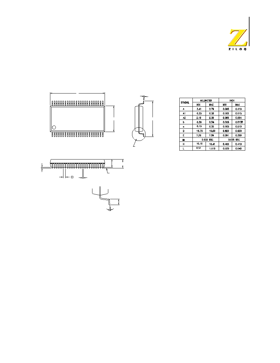
Z86D990/Z86D991 OTP and Z86L99X ROM
Low-Voltage Microcontrollers with ADC
PS003807-1002
P R E L I M I N A R Y
91
Packaging
Figure 37 through Figure 40 show the available packages.
Figure 37. 48-Pin SSOP
CONTROLLING DIMENSIONS : MM
LEADS ARE COPLANAR WITHIN .004 INCH
D
E
H
A1
A2
A
e
SEATING PLANE
b
48
25
c
Detail A
Detail A
0-8∞
L
1
24
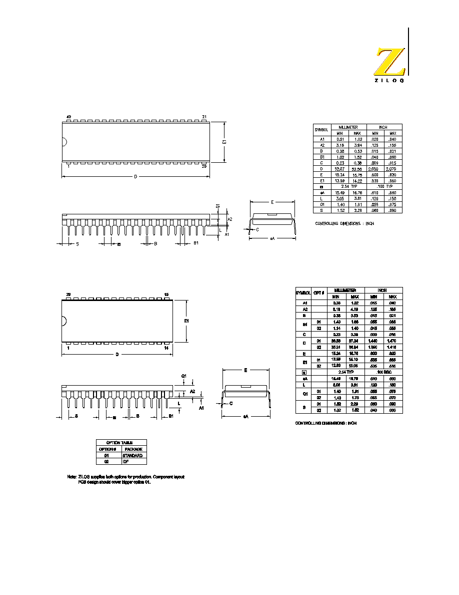
Z86D990/Z86D991 OTP and Z86L99X ROM
Low-Voltage Microcontrollers with ADC
PS003807-1002
P R E L I M I N A R Y
92
Figure 38. 40-Pin PDIP
Figure 39. 28-Pin PDIP
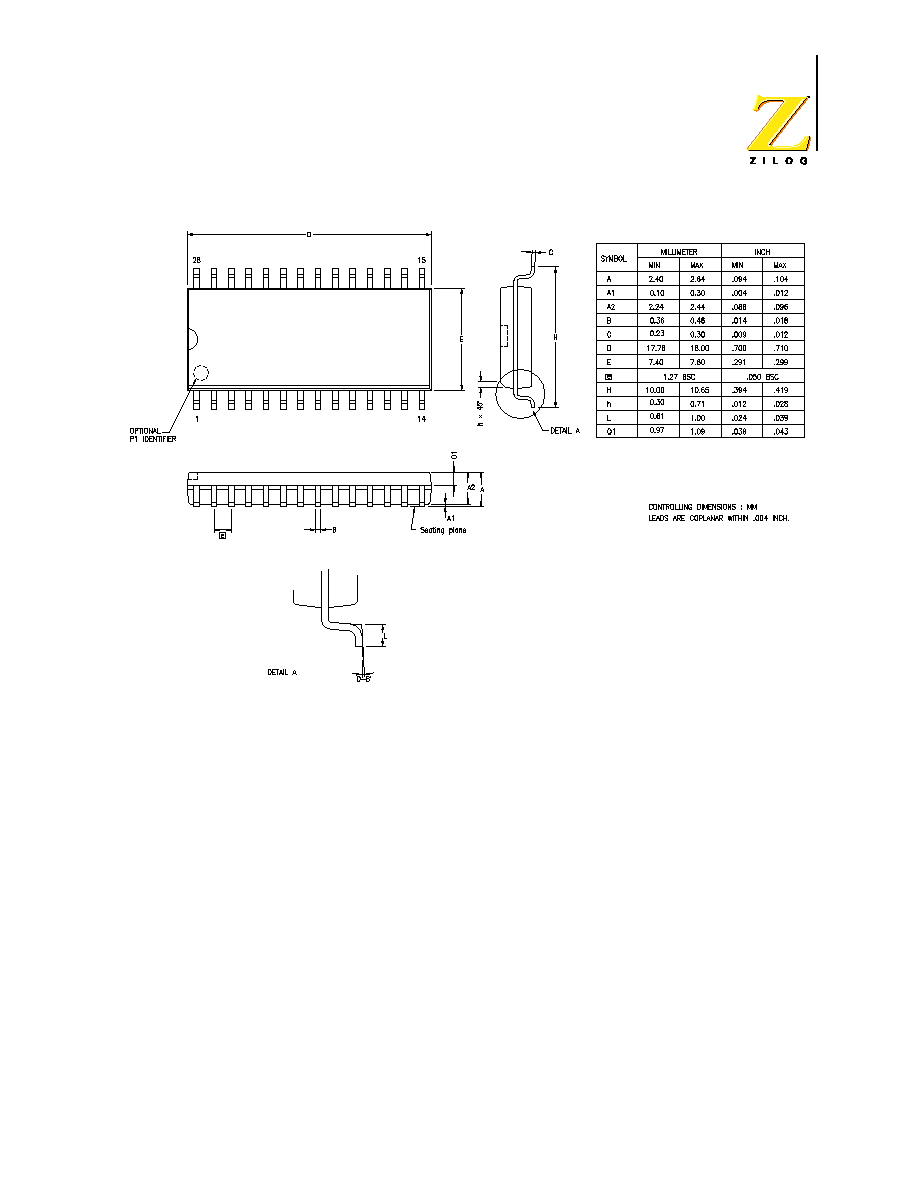
Z86D990/Z86D991 OTP and Z86L99X ROM
Low-Voltage Microcontrollers with ADC
PS003807-1002
P R E L I M I N A R Y
93
Figure 40. 28-Pin SOIC

Z86D990/Z86D991 OTP and Z86L99X ROM
Low-Voltage Microcontrollers with ADC
PS003807-1002
P R E L I M I N A R Y
94
Design Considerations
The Z8 uses a Pierce oscillator with an internal feedback circuit. The advantages
of this circuit are low cost, large output signal, low-power level in the crystal, stabil-
ity with respect to V
CC
and temperature, and low impedances (not disturbed by
stray effects.)
One drawback is the requirement for high gain in the amplifier to compensate for
feedback path losses. Traces connecting crystal, capacitors, and the Z8 oscillator
pins must be as short and wide as possible. Short and wide traces reduce para-
sitic inductance and resistance. The components (capacitors, crystal, and resis-
tors) must be placed as close as possible to the oscillator pins of the Z8.
The traces from the oscillator pins of the integrated circuit (IC) and the ground
side of the lead capacitors must be guarded from all other traces (clock, V
CC
, and
system ground) to reduce cross-talk and noise injection. Guarding the traces is
usually accomplished by keeping other traces and system ground trace planes
away from the oscillator circuit and by placing a Z8 device V
SS
ground ring around
the traces/components. The ground side of the oscillator lead capacitors must be
connected to a single trace to the Z8 V
SS
(GND) pin. It must not be shared with
any other system ground trace or components except at the Z8 device V
SS
pin.
Not sharing the ground side of the oscillator lead capacitors is to prevent differen-
tial system ground noise injection into the oscillator.

Z86D990/Z86D991 OTP and Z86L99X ROM
Low-Voltage Microcontrollers with ADC
PS003807-1002
P R E L I M I N A R Y
95
Ordering Information
For fast results, contact your local ZiLOG sale offices for assistance in ordering
part(s). Updated information can be found on the ZiLOG website:
HTTP
://
WWW
.Z
I
LOG.
COM
Precharacterization Product
The product represented by this document is newly introduced and ZiLOG has not
completed the full characterization of the product. The document states what
ZiLOG knows about this product at this time, but additional features or nonconfor-
mance with some aspects of the document might be found, either by ZiLOG or its
customers in the course of further application and characterization work. In addi-
tion, ZiLOG cautions that delivery might be uncertain at times, due to start-up yield
issues.
ZiLOG, Inc.
532 Race Street
San Jose, CA 95126-3432
Telephone: (408) 558-8500
FAX: 408 558-8300
Internet:
HTTP
://
WWW
.Z
I
LOG.
COM
Part
PSI
Description
Z86D99 (OTP)
Z86D990PZ008SC
Z86D990HZ008SC
Z86D991PZ008SC
Z86D991SZ008SC
40-pin PDIP
48-pin SSOP
28-pin PDIP
28-pin SOIC
Z86L99 (Mask ROM)
Z86L990PZ008SC
Z86L990HZ008SC
Z86L991PZ008SC
Z86L991SZ008SC
Z86L996PZ008SC
Z86L996SZ008SC
Z86L997PZ008SC
Z86L997SZ008SC
40-pin PDIP
48-pin SSOP
28-pin PDIP
28-pin SOIC
28-pin PDIP
28-pin SOIC
28-pin PDIP
28-pin SOIC
Emulator
Z86L9900100ZEM
Emulator/Programmer
Adapter
Z86D9900100ZDH
48 SSOP Adapter
Evaluation Board
Z86L9900100ZCO
Evaluation Board