
DS96WRL0501
P R E L I M I N A R Y
1-1
1
P
RELIMINARY
P
RODUCT
S
PECIFICATION
Z87000/Z87L00
1
S
PREAD
S
PECTRUM
C
ONTROLLERS
FEATURES
s
Transceiver/Controller Chip Optimized for Implement-
ation of 900 MHz Spread Spectrum Cordless Phone
�
Adaptive Frequency Hopping
�
Transmit Power Control
�
Error Control Signaling
�
Handset Power Management
�
Support of 32 kbps ADPCM Speech Coding for
High Voice Quality
s
DSP Core Acts as Phone Controller
�
Zilog-Provided Embedded Transceiver Software to
Control Transceiver Operation and Base Station-
Handset Communications Protocol
�
User-Modifiable Software Governs Phone
Features
s
Transceiver Circuitry Provides Primary Cordless Phone
Communications Functions
�
Digital Downconversion with Automatic Frequency
Control (AFC) Loop
�
FSK Demodulator
�
FSK Modulator
�
Symbol Synchronizer
�
Time Division Duplex (TDD) Transmit and Receive
Buffers
s
On-Chip A/D and D/A to Support 10.7 MHz IF Interface
s
Bus Interface to Z87010 ADPCM Processor
s
Static CMOS for Low Power Consumption
s
3.0V to 3.6V, -20
�
C to +70
�
C, Z87L00
4.5V to 5.5V, -20
�
C to +70
�
C, Z87000
s
16.384 MHz Base Clock
GENERAL DESCRIPTION
The Z87000/Z87L00 FHSS Cordless Telephone Trans-
ceiver/Controllers are expressly designed to implement a
900 MHz frequency hopping spread spectrum cordless
telephone compliant with United States FCC regulations
for unlicensed operation. The Z87000 and Z87L00 are dis-
tinct 5V and 3.3V versions, respectively, of the device. For
the sake of brevity, all subsequent references to the
Z87000 in this document also apply to the Z87L00, unless
specifically noted.
The Z87000 supports a specific cordless phone system
design that uses frequency hopping and digital modulation
to provide extended range, high voice quality, and low sys-
tem costs.The Z87000 uses a Zilog 16-bit fixed-point two's
complement static CMOS Digital Signal Processor core as
the phone and RF section controller. The Z87000's DSP
core processor further supports control of the RF section's
frequency synthesizer for frequency hopping and the gen-
eration of the control messages needed to coordinate in-
corporation of the phone's handset and base station.
Device
ROM
(KWords)
RAM*
(Words)
I/O
Lines
Package
Information
Z87000
12
512
32
84-Pin PLCC
100-Pin QFP
Z87L00
12
512
32
100-Pin QFP
Note:
*General-Purpose

Z87000/Z87L00
Spread Spectrum Controllers
Zilog
1-2
P R E L I M I N A R Y
DS96WRL0501
GENERAL DESCRIPTION
(Continued)
Additional on-chip transceiver circuitry supports Frequen-
cy Shift Keying modulation/demodulation and multiplex-
ing/demultiplexing of the 32 kbps voice data and 4 kbps
command data between handset and base station. The
Z87000 provides thirty-two I/O pins, including four wake-
up inputs and two CPU interrupt inputs. These program-
mable I/O pins allow a variety of user-determined phone
features and board layout configurations. Additionally, the
pins may be used so that phone features and interfaces
are supported by an optional microcontroller rather than by
the Z87000's DSP core.
In combination with an RF section designed according to
the system specifications, Zilog's Z87010/Z87L10 ADPCM
Processor, a standard 8-bit PCM telephone CODEC and
minimal additional phone circuity, the Z87000 and its em-
bedded software provide a total system solution.
Figure 1. System Block Diagram of a Z87000/Z87010 Based Phone
Z87010
ADPCM
Processor
Z87000
Spread
Spectrum
Controller
RF Section
Z87010
ADPCM
Processor
Z87000
Spread
Spectrum
Controller
RF Section
Telephone
Line
Interface
Base Station
Handset
CODEC
CODEC

Z87000/Z87L00
Zilog
Spread Spectrum Controllers
DS96WRL0501
P R E L I M I N A R Y
1-3
1
Figure 2. Z87000 Functional Block Diagram
Digital
DSP Core
12K Words
Program ROM
256 Word
RAM 0
256 Word
RAM 1
Port 0
Port 1
ADC
(1-bit)
ADC
(8-bit)
DAC
(4-bit)
DAC
(4-bit)
FSK Demodulator
FSK Modulator
(downconverter, limiter discriminator,
AFC, bit sync, frame sync, SNR
detector)
Frame Counter(s),
Event Trigger,
T/R Switch Ctrl,
Power On/Off Ctrl,
Analog
Power
Receive
Rate
Buffer
Transmit
Rate
Buffer
Z87010
Interface
Antenna Select
RX
VREF
TX
RXON
RFRX
RFTX
RFEON
SYLE
RSSI
PWLV
ANT0
ANT1
HBSW
RESETB
TEST
AVDD
AGND
VDD
GND
P1[15..0]
P0[15..0]
VXDATA[7..0]
VXADD[2..0]
VXSTRB
VXRWB
VXRDYB
CLKOUT
CODCLK
Power

Z87000/Z87L00
Spread Spectrum Controllers
Zilog
1-4
P R E L I M I N A R Y
DS96WRL0501
PIN DESCRIPTION
Figure 3. 84-Pin PLCC ROM Pin Configuration (Z87000 only)
Z87000
A
VDD
RSSI
PWL
V
A
GND
RFRX
RXON
SYLE
VDD
MCLK
GND
/RESETB
CODCLK
VXADD0
VXADD1
VXADD2
VDD
VXR
WB
VXSTRB
VXRD
YB
GND
RFTX
VXDATA0
VXDATA1
VXDATA2
VDD
VXDATA3
VXDATA4
VXDATA5
VXDATA6
VXDATA7
CLKOUT
HBSW
GND
TEST
VDD
ANT0
ANT1
P00
P01
GND
P02
P03
P04
P05
VDD
P06
P07
P08
P09
GND
P010
P011
P012
P013
VDD
P014
P015
P10
P11
GND
P12
P13
P14
AGND
TX
RX
AVDD
VREF
RFEON
P115
GND
P114
P113
P112
VDD
P111
P110
P19
GND
P18
P17
P16
VDD
P15
1
12
33
54
75

Z87000/Z87L00
Zilog
Spread Spectrum Controllers
DS96WRL0501
P R E L I M I N A R Y
1-5
1
Table 1. 84-Pin PLCC Pin Description Summary
Pin Number
Symbol
Function
Direction
1,19,27,36,46,
56,63,75
GND
Ground
�
2
MCLK
Master clock (16.384 MHz)
Input
3,23,31,41,51,
61,71,79
V
DD
Digital
�
4
RFTX
RF transmit switch control
Output
5
SYLE
RF synthesizer load enable
Output
6
RXON
Demodulator "on" indication
Output
7
RFRX
RF receive switch control
Output
8,13
AGND
Analog ground
�
9
PWLV
RF transmit power level
Output
10
RSSI
RF receive signals strength indicator
Input
11,15
AV
DD
Analog V
DD
�
12
TX
Analog transmit IF signal
Output
14
RX
Analog receive IF signal
Input
16
V
REF
Analog reference voltage for RX signal
Output
17
RFEON
RF module on/off control
Output
18,20,21,22,24,
25,26,28,29,30,
32,33,34,35,37,38
P115
General-purpose
Input
59,60
ANT1
RF diversity antenna control
Input/Output
62
TEST
Main test mode control
Input
64
HBSW
Handset/Base Control
�
65
CLKOUT
Clock output to ADPCM Processor
Output
76
VXRDYB
ADPCM processor ready signal
Output
77
VXSTRB
ADPCM processor data strobe
Input
78
VXRWB
ADPCM read/write control
Input
80,81,82
VXADD2
ADPCM processor address bus
Input
83
CODCLK
Clock output to codec
Output
84
/RESETB
Reset signal
Input

Z87000/Z87L00
Spread Spectrum Controllers
Zilog
1-6
P R E L I M I N A R Y
DS96WRL0501
PIN DESCRIPTION
(Continued)
Figure 4. 100-Pin QFP Pin Configuration
Z87000/Z87L00
AVDD
RSSI
PWL
V
A
GND
RFRX
RXON
SYLE
VDD
MCLK
GND
RESETB
CODCLK
VXADD0
VXADD1
VXADD2
VDD
VXR
WB
VXSTRB
VXRD
YB
GND
RFTX
VXDATA0
VXDATA1
VXDATA2
VDD
VXDATA3
VXDATA4
VXDATA5
VXDATA6
VXDATA7
CLKOUT
HBSW
GND
TEST
VDD
ANT0
ANT1
P00
P01
GND
P02
P03
P04
P05
VDD
P06
P07
P08
P09
GND
P010
P011
P012
P013
VDD
P014
P015
P10
P11
GND
P12
P13
P14
AGND
TX
RX
AVDD
VREF
RFEON
P115
GND
P114
P113
P112
VDD
P111
P110
P19
GND
P18
P17
P16
VDD
P15
N/C
N/C
N/C
N/C
N/C
N/C
N/C
N/C
N/C
N/C
N/C
N/C
N/C
N/C
N/C
N/C
1
81
31
51

Z87000/Z87L00
Zilog
Spread Spectrum Controllers
DS96WRL0501
P R E L I M I N A R Y
1-7
1
Table 2. 100-Pin QFP Pin Configuration
No
Symbol
Function
Direction
1,8
AV
DD
Analog V
DD
�
2,3,4,15,27,28,
29,40,52,53,54,
66,77,78,79,90
N/C
No connection
�
5
TX
Analog transmit IF signal
Output
6,98
AGND
Analog ground
�
7
RX
Analog receive IF signal
Input
9
VREF
Analog reference voltage for RX signal
�
10
RFEON
RF module on/off control
Output
11,13,14,16,18,
19,20,22,23,23,
26,30,31,32,34,35
P1[15..0]
General-purpose I/O port 0
Input
17,25,38,49,62,
73,84,93
V
DD
Digital
�
36,37,39,41,42,
43,45,46,47,48,
50,51,55,56,58,59
P0[15..0]
General-purpose I/O port 0
Input
60,61
ANT[1..0]
RF diversity antenna control
Input/Output
63
TEST
Main test mode control
Input
65
HBSW
Handset/bast control
Input
67
CLKOUT
Clock output to ADPCM processor
Output
68,69,70,71,72,
74,75,76
VXDATA[7..]
ADPCM processor data bus
Input
81
VXRDYB
ADPCM processor ready signal
Output
82
VXSTRB
ADPCM processor data strobe
Input
83
VXRWB
ADPCM processor read/write control
Input
85,86,87
VXADD[2..0]
ADPCM processor address bus
Input
88
CODCLK
Clock output to codec
Output
89
/RESETB
Reset signal
Input
92
MCLK
Master clock input (16.384 MHz)
Input
94
RFTX
RF transmit switch control
Output
95
SYLE
RF synthesizer load enable
Output
96
RXON
Demodulator "on" indication
Output
97
RFRX
RF receive switch control
Output
99
PWLV
RF transmit power level
Input
100
RSSI
RF receive signal strength indicator
Input

Z87000/Z87L00
Spread Spectrum Controllers
Zilog
1-8
P R E L I M I N A R Y
DS96WRL0501
ABSOLUTE MAXIMUM RATINGS
Stresses greater than those listed under Absolute Maxi-
mum Ratings may cause permanent damage to the de-
vice. This is a stress rating only; operation of the device at
any condition above those indicated in the operational sec-
tions of these specifications is not implied. Exposure to ab-
solute maximum rating conditions for extended period may
affect device reliability.
STANDARD TEST CONDITIONS
The electrical characteristics listed below apply for the fol-
lowing standard test conditions, unless otherwise noted.
All voltages are referenced to GND. Positive current flows
into the referenced pins. Standard test conditions are as
follows:
s
3.0V < V
DD
< 3.6V (Z87L00)
s
4.5V < V
DD
< 5.5V (Z87000)
s
GND = 0V
s
T
A
= -20 to +70
�
C
Symbol Parameter
Min
Max
Units
V
DD
, AV
DD
DC Supply
Voltage(1)
-0.5
7.0
V
V
IN
Input Voltage(2)
-0.5 V
DD
+ 0.5
V
V
OUT
Output Voltage(3)
-0.5 V
DD
+ 0.5
V
T
A
Operating
Temperature
-20
+70
�
C
T
STG
Storage
Temperature
-65
+150
�
C
Notes:
1. Voltage on all pins with respect to GND.
2. Voltage on all inputs WRT VDD
3. Voltage on all outputs WRT VDD
Figure 5. Test Load Diagram
Output
Under
Test
IoL
IoH
Threshold
Voltage
50pF

Z87000/Z87L00
Zilog
Spread Spectrum Controllers
DS96WRL0501
P R E L I M I N A R Y
1-9
1
RECOMMENDED OPERATING CONDITIONS
Table 3. 5V
�
0.5V Operation (Z87000)
Symbol
Parameter
Min
Max
Units
V
DD
, AV
DD
Supply Voltage
4.5
5.5
V
V
IH
Input High Voltage
2.0
V
DD
+ 0.3
V
V
IL
Input Low Voltage
GND -0.3
0.8
V
I
OH
Output High Current
-2.0
mA
I
OL1
Output Low Current
4.0
mA
I
OL2
Output Low Current, Ports (limited usage, 1)
12.0
mA
T
A
Operating Temperature
-20
+70
�
C
Notes:
1. Maximum 3 pins total from P0[15..0] and P1[15..0]
Table 4. 3.3V
�
0.3V Operation (Z87L00)
Symbol
Parameter
Min
Max
Units
V
DD
Supply Voltage
3.0
3.6
V
V
IH
Input High Voltage
0.7 V
DD
V
DD
+0.3
V
V
IL
Input Low Voltage
GND -0.3
0.1 V
DD
V
I
OH
Output High Current
-1.0
mA
I
OL1
Output Low Current
2.0
mA
I
OL2
Output Low Current, Ports (limited usage, 2)
6.0
mA
T
A
Operating Temperature
-20
+70
�
C
Notes:
1. Maximum 3 pins total from P0[15..0] and P1[15..0]

Z87000/Z87L00
Spread Spectrum Controllers
Zilog
1-10
P R E L I M I N A R Y
DS96WRL0501
DC ELECTRICAL CHARACTERISTICS
Conditions for DC characteristics are corresponding oper-
ating conditions, and standard test conditions, unless oth-
erwise specified.
Table 5. 5V
�
0.5V Operation (Z87000)
Symbol
Parameter
Test Condition
Min
Max
Units
V
OH
Output High Voltage
V
DD
min, I
OH
max
2.4
V
V
OL1
Output Low Voltage
V
DD
min, I
OL1
max
0.6
V
V
OL2
Output Low Voltage, Ports (1)
V
DD
min, I
OL2
max
1.2
V
I
L
Input Leakage
V
IN
= 0V, V
DD
-2
2
�
A
I
CC
Supply Current
80
mA
I
CC2
Standby Mode Current (2)
4
mA
Notes:
1. Maximum 3 pins total from P0[15..0] and P1[15..0]
2. 2.3 mA typical at 25
�
C, 5 volts.
Table 6. 3.3V
�
0.3V Operation (Z87L00)
Symbol
Parameter
Test Condition
Min
Max
Units
V
OH
Output High Voltage
V
DD
min, I
OH
max
1.6
V
V
OL1
Output Low Voltage
V
DD
min, I
OL1
max
0.4
V
V
OL2
Output Low Voltage, Ports(1)
V
DD
min, I
OL2
max
1.2
V
I
L
Input Leakage
V
IN
= 0V, V
DD
-2
2
�
A
I
CC
Supply Current
55
mA
I
CC2
Standby Mode Current(2)
1.4
mA
Notes:
1. Maximum 3 pins total from P0[15..0] and P1[15..0]
2. 1.6 mA typical at 25
�
C, 3.3 volts.

Z87000/Z87L00
Zilog
Spread Spectrum Controllers
DS96WRL0501
P R E L I M I N A R Y
1-11
1
ANALOG CHARACTERISTICS
Table 7. 1-Bit ADC (Temperature: -20/+70
�
C)
Parameter
Minimum
Typical
Maximum
Units
Resolution
-
1
-
bit
Power dissipation
0.54
(70
�
c)
1.0
(40
�
c)
2.75
(-20
�
c)
mW
Power dissipation, Stop mode
0.06
(70
�
c)
0.2
(40
�
c)
1.1
(-20
�
c)
mW
Sample frequency
-
8.192
-
MHz
Sample window(1)
29
31
33
ns
Bandwidth
-
60
-
MHz
Supply Range(=AV
DD
)
Z87L00
Z87000
3.0
4.5
3.6
5.5
V
V
Acquisition time
2
3
8
ns
Settling time
8
10
18
ns
Conversion time
4
6
18
ns
Aperture delay
2
3
8.5
ns
Aperture uncertainty(2)
-
-
0.5
ns
Input voltage range (p-p)
800
1000
1200
mV
Reference voltage
Z87L00
Z87000
1.7 (AV
DD
= 3V)
2.7 (AV
DD
=4.5V)
1.9 (AV
DD
= 3.3V)
3.0 (AV
DD
= 5V)
2.1 (AV
DD
= 3.6V)
3.3 (AV
DD
= 5.5V)
V
V
Input resistance
10
18
25
KOhm
Input capacitance
-
10
-
pF
Notes:
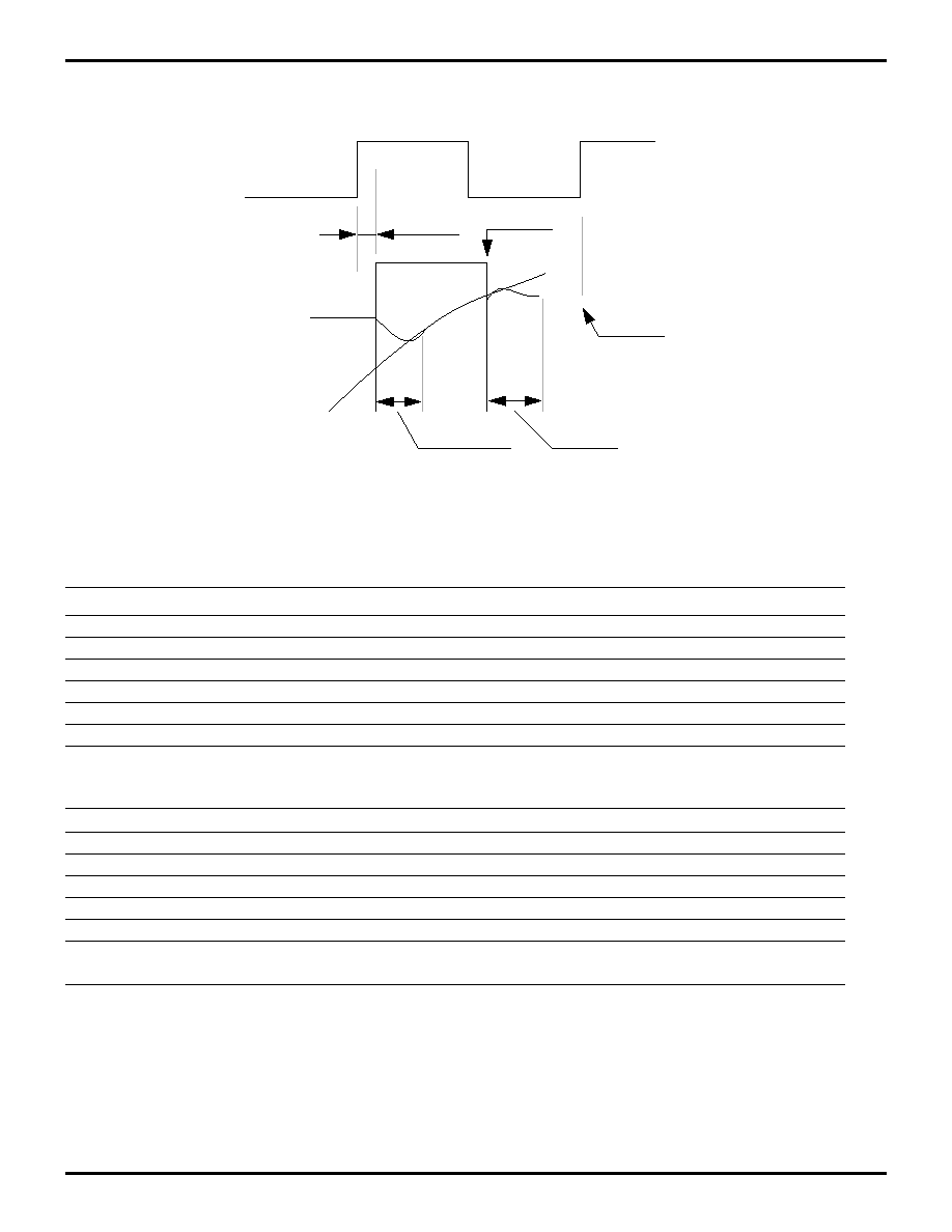
Window of time while input signal is applied to sampling capacitor; see next figure.
Uncertainty in sampling time due to random variations such as thermal noise.
Z87000/Z87L00
Spread Spectrum Controllers
Zilog
1-12
P R E L I M I N A R Y
DS96WRL0501
ANALOG CHARACTERISTICS (Continued)
Figure 6. 1-Bit ADC Definition of Terms
Acquisition
Time
Settling
Time
Conversion
Time (for
+
Latched
Output
CLK (16.384MHz)
SAMPLING
WINDOW
Aperture
Delay
INPUT
SIGNAL
digital output)
Sampling
Table 8. 8-bit ADC (Temperature -20/+70
�
C)
Parameter
Minimum
Typical
Maximum
Units
Resolution
-
6
-
bit
Integral non-linearity
-
0.5
1
LSB
Differential non-linearity
-
-
0.5
LSB
Power Dissipation (peak)
35
70
mW
Sample window
5
-
120
ns
Bandwidth
-
-
2
Msps
Supply Range (=AV
DD
)
Z87L00
Z87000
3.0
4.5
3.3
5.0
3.6
5.5
V
V
Input voltage range
0-AV
DD
V
Conversion time
0.5
-
-
�
s
Aperture delay
2
3
8.5
ns
Aperture uncertainty
-
-
1
ns
Input resistance
-
25
-
Kohm
Input capacitance
-
10
-
pF
Notes:
1. 8-bit ADC only tested for 6-bit resolution.

Z87000/Z87L00
Zilog
Spread Spectrum Controllers
DS96WRL0501
P R E L I M I N A R Y
1-13
1
Table 9. 4-bit DAC (Temperature: -20/+70
�
C)
Parameter
Minimum
Typical
Maximum
Units
Resolution
-
4
-
bit
Integral non-linearity
-
0.25
0.5
LSB
Differential non-linearity
-
0.25
1
LSB
Settling time (1/2 LSB)
-
-
22.5
ns
Zero error at 25
�
C
-
1
2
mV
Conversion time (input change to output change)
14
19
76
ns
Power dissipation, 25 pF load
1.2
(70
�
c)
20
(40
�
c)
24.1
(-20
�
c)
mW
Power dissipation, 25 pF load, Stop mode
0.18
(70
�
c)
1.0
(40
�
c)
1.1
(-20
�
c)
mW
Conversion time (input change to output change)
14.5
19.1
75.8
ns
Rise time (full swing)
11
15
71
ns
Output slew rate
8
67
96
V/
�
s
Output voltage range
-
0.2 AV
DD
to 0.6AV
DD
-
V
Supply Range (=AV
DD
)
Z87L00
Z87000
3.0
4.5
3.3
5.0
3.6
5.5
V
V
Output load resistance
330
Ohm
Output load capacitance
-
25
-
pF

Z87000/Z87L00
Spread Spectrum Controllers
Zilog
1-14
P R E L I M I N A R Y
DS96WRL0501
INPUT/OUTPUT PIN CHARACTERISTICS
All digital pins (all pins except V
DD
, AV
DD
, GND, AGND,
V
REF
, RX, TX, RSSI and PWLV) have an internal capaci-
tance of 5 pF.
The RX analog input pin has an input capacitance of 10
pF.
The RSSI analog input pin has an input capacitance of 10
pF.
AC ELECTRICAL CHARACTERISTICS
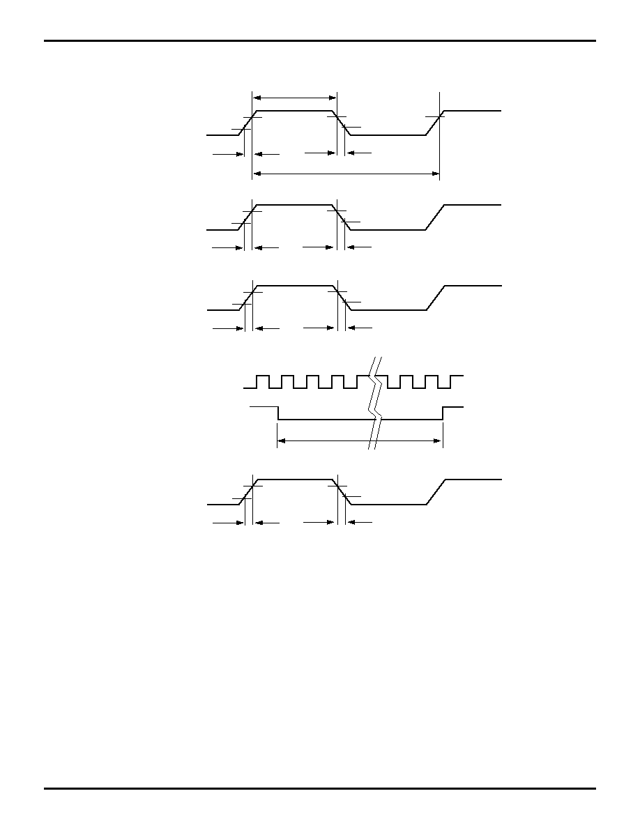
Clocks, Reset and RF Interface
Table 10. Clocks, Reset and RF Interface
No.
Symbol
Parameter
Min
Max
Units
1
TpC
MCLK input clock period (1)
61
61
ns
2
TwC
MCLK input clock pulse width
20
40
ns
3
TrC, TfC
MCLK input clock rise/fall time
15
ns
4
TrCC, TfCC
CLKOUT output clock rise/fall time
2
6
ns
5
TrCO, TfCO
CODCLK output clock rise/fall time
2
6
ns
6
TwR
RESETB input low width
18
TpC
7
TrRF, TfRF
RF output controls rise/fall time (2)
2
6
ns
Notes:
1. MCLK is 16.384 MHz
�
25 ppm
2. RF Controls are RFTX, RFRX, RXON, RFEON, SYLE.

Z87000/Z87L00
Zilog
Spread Spectrum Controllers
DS96WRL0501
P R E L I M I N A R Y
1-15
1
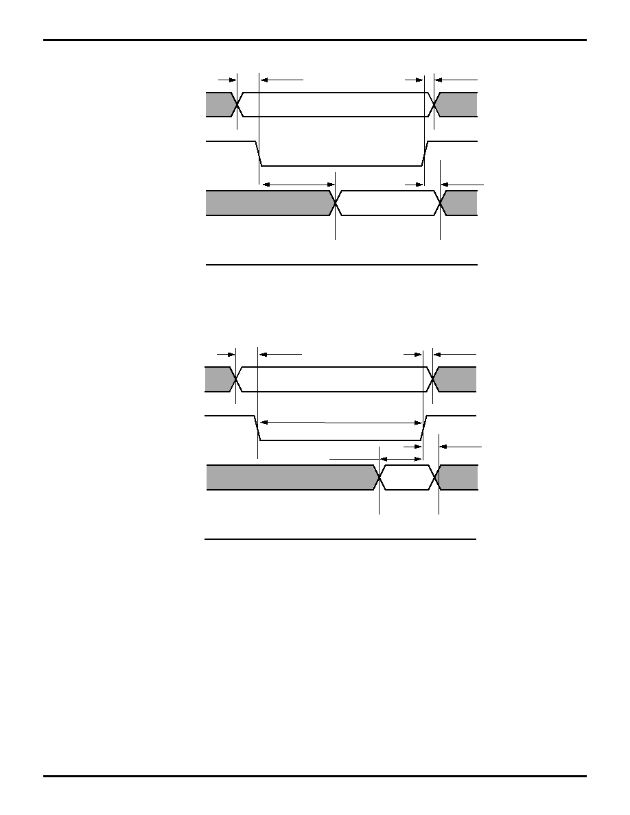
ADPCM Processor Interface
The Z87000 is a peripheral device for the ADPCM Proces-
sor. The interface from the Z87000 perspective is com-
posed of an input address bus, a bidirectional data bus,
strobe and read/write input control signals and a
ready/wait output control signal.
READ CYCLES refer to data transfers from the Z87000 to
the ADPCM Processor.
WRITE CYCLES refer to data transfers from the ADPCM
Processor to the Z87000.
Table 11. Read Cycles
Signal Name
Function
Direction
VXADD[2..0]
Address Bus
ADPCM Proc. to Z87000
VXDATA[7..0]
Data Bus
Bidirectional
VXSTRB
Strobe Control Signal
ADPCM Proc. to Z87000
VXRWB
Read/Write Control Signal
ADPCM Proc. to Z87000
VXRDYB
Ready Control Signal
Z87000 to ADPCM Proc.
Table 12. Write Cycles
No.
Symbol
Parameter
Min
Max
Units
8
TsAS
Address, Read/Write setup time before Strobe falls
10
ns
9
ThSA
Address, Read/Write hold time after Strobe rises
3
ns
10
TaDrS
Data read access time after Strobe falls
30 (1)
ns
11
ThDrS
Data read hold time after Strobe rises
8.5
40 (2)
ns
12
TwS
Strobe pulse width
20
13
TsDwS
Data write setup time before Strobe rises
10
ns
14
ThDwS
Data write hold time after Strobe rises
3
ns
15
TaDrRY
Data read valid before Ready falls
22
ns
16
TdSRY
Strobe high after Ready falls
0
ns
Notes:
1. Requires wait state on ADPCM Processor read cycles
2. Requires no write cycle directly following read cycle on ADPCM Processor
Z87000/Z87L00
Spread Spectrum Controllers
Zilog
1-16
P R E L I M I N A R Y
DS96WRL0501
AC TIMING DIAGRAMS
Figure 7. Transceiver Output Signal
TpC (1)
TfC(3)
TrC(3)
TwC(2)
MCLK
MCLK
RESETB
1
2
3
4
18
17
16
TfCC(4)
TrCC(4)
CLKOUT
TfCO(5)
TrCO(5)
CODCLK
TwR(6)
TfRF(7)
TrRF(7)
RFTX
RFRX
RXON
RFEON
SYLE
Z87000/Z87L00
Zilog
Spread Spectrum Controllers
DS96WRL0501
P R E L I M I N A R Y
1-17
1
Figure 8. Read/Write Cycle TImings
VXADD
VXRWB
VXSTRB
VXDATA
VXRDYB
VXDATA Write Cycle
TsAS(8)
ThSA(9)
ThDwS(14)
VXADD
VXRWB
VXSTRB
VXDATA
VXRDYB
VXDATA Read Cycle
TsAS(8)
ThSA(9)
ThDrS(11)
TaDrS(10)
TsDwS(13)
TwS(12)

Z87000/Z87L00
Spread Spectrum Controllers
Zilog
1-18
P R E L I M I N A R Y
DS96WRL0501
AC TIMING DIAGRAMS (Continued)
Figure 9. Read/Write Cycle Timing with Wait State
VXRDYB
VXDATA Write Cycle with Wait State
VXADD
VXRWB
VXSTRB
VXDATA
VXRDYB
VXDATA Read Cycle with Wait State
TsAS(8)
ThSA(9)
ThDrS(11)
TaDrRY(15)
VXADD
VXRWB
VXSTRB
VXDATA
TsAS(8)
ThSA(9)
ThDwS(14)
TsDwS(13)
TwS(12)
TdSRY(16)
TdSRY(16)

Z87000/Z87L00
Zilog
Spread Spectrum Controllers
DS96WRL0501
P R E L I M I N A R Y
1-19
1
PIN FUNCTIONS
V
DD.
Digital power supply.
GND. Digital ground.
AV
DD
. Analog power supply.
AGND. Analog ground.
V
REF
(analog reference). This signal is the reference volt-
age used by the high speed analog comparator to sample
the RX input signal.
RX (analog input). This is the RX IF receive signal from
the RF module, input to the analog comparator and FSK
demodulator. It is internally biased to the V
REF
DC voltage.
The IF signal from the RF module should be AC coupled
to the RX pin.
TX (analog output). This is the IF transmit signal to the RF
module, output from the FSK modulator and transmit 4-bit
D/A converter.
RXON (output; active high or low programmable). This
pin reflects the programming of the demodulator turn-on
time.
RFRX (output; active high or low programmable). Control
for the receive switch on the RF module. Active during re-
ceive periods.
RFTX (output; active high or low programmable). Control
for the transmit switch on the RF module. Active during
transmit periods.
RFEON (output; active high or low programmable).
On/off control for the RF module. Active (on) during wake
periods. Inactive (off) during sleep periods on the handset.
RSSI (analog input). Receive signal strength indicator
from RF module, input to the RSSI 8-bit ADC.
PWLV (analog output). Power level control for RF module,
output from the transmit power 4-bit DAC.
SYLE (output). RF synthesizer load enable: latches new
frequency hopping control word of external RF synthesiz-
er. Programmable polarity.
ANT[1..0] (output). Control for optional antenna diversity
on the RF module.
MCLK (input). Master clock input.
CLKOUT (output). Clock output for external ADPCM pro-
cessor.
CODCLK (output). Clock output for external voice CO-
DEC.
/RESETB (input, active low). Reset signal.
VXADD[2..0] (input). Address bus controlled by external
ADPCM processor. The Z87000 acts as peripheral of the
Z87010 ADPCM processor.
VXDATA[7..0](input/output). Read/write data bus con-
trolled by external Z87010 ADPCM processor.
VXSTRB (input). Data strobe signal for the VXDATA bus,
controlled by external Z87010.
VXRWB (input). Read/write control for the VXDATA bus,
controlled by external Z87010.
VXRDYB (output, active low). Ready control for the VX-
DATA bus. This signal is driven high (de-asserted) by the
Z87000 to insert wait states in the Z87010 ADPCM proces-
sor accesses.
TEST (input, active high). Main test mode control. Must be
set to GND.
HBSW (input with internal pull-up). Control for hand-
set/base configuration. Must be driven high or not connect-
ed for handset, low for base.
P0[15..0] (input/output). General-purpose I/O port. Direc-
tion is bit-programmable. Pins P0[3..0],when configured in
input mode, can also be individually programmed as wake-
up pins for the Z87000 (wake-up active low; signal internal-
ly debounced and synchronized to the bit clock).
P1[15..0] (input/output).General-purpose I/O port. Direc-
tion is bit-programmable. Pins P114 and P115, when con-
figured in input mode, also behave as individually
maskable interrupt pins for the core processor (positive
edge-triggered).
P0 0
WAKEUP0
P0 1
WAKEUP1
P0 2
WAKEUP2
P0 3
WAKEUP3
P1 14
INT0
P1 15
INT2

Z87000/Z87L00
Spread Spectrum Controllers
Zilog
1-20
P R E L I M I N A R Y
DS96WRL0501
FUNCTIONAL DESCRIPTION
The functional partitioning of the Z87000 is shown in Fig-
ure 2. The chip consists of a receiver, a transmitter, and
several additional functional blocks.
The receiver consists of the following blocks:
s
Receive 1-bit ADC
s
Demodulator, including:
�
IF Downconverter
�
AFC (Automatic Frequency Control)
�
Limiter-Discriminator
�
Matched Filter
�
Bit Synchronizer
�
Bit Inversion
�
Frame Synchronizer (unique word detector)
�
SNR Detector
s
Receive Frame Timing Counter
s
Receive Buffer and Voice Interface
The Transmitter Consists of the Following Blocks:
s
Transmit Buffer and Voice Interface
s
Transmit Frame Timing Counter (used on base station
only)
s
Modulator, including:
�
NCO
�
Bit Inversion
s
Transmit 4-Bit DAC
In Addition, there are the following Shared Blocks.
s
Event Trigger Block, Controlling:
�
Transmit/Receive Switch
�
Power On/Off Switches (Modulator, Demodulator,
RF Module)
�
Antenna Switch Control (used on Base Station
only for Antenna Diversity)
s
4-Bit DAC for Setting Transmit Power Level
s
8-Bit ADC for Sampling the Received Signal Strength
Indicator (RSSI)
s
DSP Core Processor
s
Two 16-Bit General-Purpose I/O Ports
s
Z87010 ADPCM Processor Interface
Basic Operation
The transmitter and receiver operate in time-division du-
plex (TDD): handset and base station transmit and receive
alternately. The TDD duty cycle lasts 4 ms and consists of
the following events:
s
At the beginning of the cycle, the frequency is changed
(hopping)
s
The base station transmits a frame of 144 bits while the
handset receives
s
The handset then transmits a frame of 148 bits while the
base receives.
Figure 1. Basic Time Duplex Timing
BASE
HANDSET
TX
RX
TX
RX
TDD switching
HOP
4ms frame
Frequency
Hopping
guard time
guard time
144 bits
148 bits

Z87000/Z87L00
Zilog
Spread Spectrum Controllers
DS96WRL0501
P R E L I M I N A R Y
1-21
1
Receive 1-Bit ADC
The incoming receive signal at the RX analog input pin is
sampled by a 1-bit analog-to-digital converter at 8.192
MHz.
The receive signal is FSK-modulated (Frequency Shift
Keying) with a carrier frequency of 10.7 MHz (Intermediate
Frequency, or IF). The instantaneous frequency varies be-
tween 10.7 MHz plus or minus 32.58 kHz. Since the data
rate is 93.09 kbps, there are 88 samples per data bit. This
oversampled data is further processed by the demodulator
to retrieve the baseband information.
The 1-bit converter is implemented with a fast comparator,
which determines whether the RX signal is larger or small-
er than a reference signal (VREF). The Z87000 internally
generates the DC level of both VREF and RX input pins.
The received signal at 10.7 MHz should thus be AC cou-
pled to the RX pin via a coupling capacitor. To ensure ac-
curate operation of the converter, the user should also at-
tach to the VREF pin a network whose impedance
matches the DC impedance seen by the RX pin.
Demodulator
The demodulator includes a two-stage IF downconverter
that brings the sampled receive signal to baseband.
The narrow-band 10.7 MHz receive signal, sampled at
8.192 MHz by the 1-bit ADC, provides a 2.508 MHz useful
image. The first local oscillator used to downconvert this IF
signal is obtained from a Numerically Controlled Oscillator
(NCO) internal to the Z87000, at the nominal frequency of
460 kHz. The resulting signal is thus at 2.048 MHz (= 2.508
MHz - 460 kHz). A second downconversion by a 2.048
MHz signal brings the receive signal to baseband.
The exact frequency of the 460 kHz NCO is slightly adjust-
ed by the Automatic Frequency Control (AFC) loop for ex-
act downconversion of the end signal to the zero frequen-
cy. The AFC circuit detects any DC component in the
output of the limiter-discriminator (see below) when receiv-
ing a known sequence of data (preamble). This DC com-
ponent is called the "frequency bias". The bias estimate
out of the AFC can be read by the DSP processor on every
frame and subsequently filtered. The processor then adds
or subtract this filtered bias to/from the NCO control word
to correct the NCO frequency output.
The main element of the demodulator is its limiter-discrim-
inator. The limiter-discriminator detects the frequency vari-
ations (ideally up to
�
32.58 kHz) and converts them to "0"
or "1" information bits. First, the data is processed through
low-pass filters to eliminate high frequency spurious com-
ponents introduced by the 1-bit ADC. The resulting signal
is then differentiated and fed to a matched filter. In the
matched filter, an integrate-and-dump operation is per-
formed to extract the digital information from its back-
ground noise.
The symbol clock is provided by the bit synchronizer. The
bit synchronizer circuit detects 0-to-1 and 1-to-0 transitions
in the incoming data stream in order to synchronize a dig-
ital phase-lock loop (DPLL). The PLL output is the recov-
ered bit clock, used to time the receiver on the base sta-
tion, and both receiver and transmitter on the handset.
To ensure enough transitions in the voice data stream, a
pseudo-random bit inversion operation is performed on the
outgoing voice data. The inversion is then reversed on the
demodulated data.
Figure 2. Demodulator Block Diagram
Rx signal
460 kHz
+ bias
1-bit
ADC
NCO
AFC
2.048 MHz
Filter
Limiter-
Discriminator
SNR
Bit
Sync
Frame
Sync
Rx
Buffer
SSB

Z87000/Z87L00
Spread Spectrum Controllers
Zilog
1-22
P R E L I M I N A R Y
DS96WRL0501
FUNCTIONAL DESCRIPTION (Continued)
Since the data is packed in frames sent alternately from
base and handset every 4 ms (TDD), additional synchroni-
zation means are necessary. This is realized in a frame
synchronizer, based on detection of a "unique word" fol-
lowing the preamble.
The receiver also features a signal-to-noise ratio detector,
which allows the DSP software to detect noisy channels
and eliminate them from the frequency hopping cycle. The
SNR information is also used by the Z87000 software as a
measure the current range between handset and base sta-
tion. This information allows the adaptive power control al-
gorithm to provide sufficient output power to the RF trans-
mitter.
Receive Frame Counter
The receive frame counter is responsible to keep track of
time within the frame. It is initialized by the frame synchro-
nizer logic on detection of the unique word. It is then
clocked by the recovered bit clock from the bit synchroniz-
er.
On the base station, the receive frame counter is used as
time base for the receiver. On the handset, it is used as
time base for both receiver and transmitter.
Receive Rate Buffer and Voice Interface
The voice signal is generated at the fixed rate of 32 kips by
the Z87010 processor, and transmitted/received in bursts
of 93.09 kips across the air. Data buffers in the transmitter
and receiver are thus necessary to absorb the rate differ-
ences over time. These buffers are called "rate buffers".
They can store up to 144 data bits and are organized as an
array of 36 4-bit nibbles.
The receive rate buffer stores the received data from the
demodulator. Incoming bits are arranged in 4-bit nibbles
and transferred to successive locations of the rate buffer.
When the last location is reached, transfers resume from
the beginning (circular buffer). The system design guaran-
tees that no buffer overrun nor enduring can occur.
The receive rate buffer can be read by the DSP core pro-
cessor of the Z87000 or by the Z87010 chip. On the
Z87000 side, the buffer can be read as a random-access
memory: the processor writes the nibble address in an ad-
dress register and reads the 4-bit data from a data register.
On the Z87010 side, a voice processor interface logic han-
dles the addressing to automatically present the succes-
sive voice nibbles to the Z87010 in the order they were re-
ceived.
Transmit Rate Buffer and Voice Interface
The transmit rate buffer stores the data to be modulated.
The data is sourced from the Z87010 or the Z87000 core
processor. As for the receive rate buffer, the Z87010 sees
a unique pipe to write to, while the Z87000 DSP core ac-
cesses the rate buffer as random-access memory. The
modulator reads from the rate buffer as from a circular
buffer.
Transmit Frame Timing Counter
On the handset, transmission does not start until the re-
ceiver has synchronized itself to the signal received from
the base station. The transmission timing is based on the
recovered clock. No additional counter is necessary.
On the base station, the situation is different. Transmission
timing is based on a local clock, while the reception's tim-
ing is based on the clock recovered from the incoming re-
ceived signal. Two counters, respectively clocked by local
and recovered clocks, are necessary to track the transmit
and receive signals.
Note that the receive clock on the base station tracks the
handset's transmit clock, which is also the handset's re-
ceive clock and tracks the transmit clock of the base sta-
tion. As a result, receive and transmit clocks of the base
station have exactly the same frequency; only their phases
differ.
Modulator
The modulator consists of a numerically controlled oscilla-
tor (NCO) which generates an FSK (Frequency Shift Key-
ing) signal at the carrier frequency of 2.508 MHz. The car-
rier frequency is shifted plus or minus 32.58 kHz for a "1"
or a "0" data bit. To facilitate conformance to FCC regula-
tions, the transitions from "1" to "0" or vice-versa are
smoothed in order to decrease the amplitude of the side
lobes of the transmit signal. In practice, the jump from one
frequency to the next is performed in several smaller
steps.
The carrier frequency is adjustable by the DSP core pro-
cessor in order to provide additional frequency adjustment
between base and handset. This is provided in case of a
frequency offset too large for possible correction by the
AFC.
The modulator also includes bit inversion logic as dis-
cussed in the receiver section.
Z87000/Z87L00
Zilog
Spread Spectrum Controllers
DS96WRL0501
P R E L I M I N A R Y
1-23
1
Transmit 4-Bit DAC
The transmit DAC clocks one new NCO value out of the
Z87000 every 8.192 MHz period. Only the 10.7 MHz alias
frequency component of the transmit signal (2.508 + 8.192
MHz image) is filtered, amplified and upconverted to the
900 MHz ISM band by the companion RF module.
Event Trigger Block
The event trigger block is responsible for scheduling the
different events happening at the bit and frame levels. The
event trigger block receives input from the frame counters
as well as the register interface of the DSP core processor.
The event trigger schedules the following events:
s
Start of the 4 ms frame: a synthesizer load enable pulse
is issued on the SYLE pin
s
Power-up of the modulator section and transmission of
the frame on handset and base station
s
Use of the bit inversion as function of mode
s
Power-up of the demodulator section and reception of
the frame on handset and base station
s
Control of RFTX and RFRX output pins, to be used as
TDD control signals switching the antenna as well as
transmitter and receiver chains on the RF module
s
Control of RFEON pin, to be used as general on/off
switch on the RF module
s
Control of the Z87000 sleep mode
4-Bit DAC for Setting Transmit Power Level
In order to save battery life, the Z87000 only transmits the
amount of RF power needed to reach the remote receiver
with a sufficient SNR margin. The on-board transmit power
4-bit DAC provides 4 different voltage levels to the power
amplifier in the RF module for that purpose. This DAC is di-
rectly controlled by the Z87000 software through an output
register.
8-Bit ADC for Sampling the Received Signal
Strength Indicator (RSSI)
RSSI information is typically generated from the last stage
of the RF receiver. The RSSI is sampled once per frame
by the 8-bit ADC and used by the Z87000 software to com-
pute the necessary Transmit Power Level voltages.
DSP Core Processor
A DSP core processor constitutes the heart of the Z87000.
The DSP runs the application software which performs the
following functions:
s
Register initialization
s
Implementation of high-level phone features; control of
phone user interface (keypad, Led, etc.)
s
Control of the Z87010 ADPCM Processor
s
Control of the phone line interface
s
Ring detection by DSP processing
s
Communication protocol between handset and base
station supporting voice and signalling channels
s
Control of the RF synthesizer and adaptive frequency
hopping algorithm
s
Control of the RF power and adaptive power algorithm
s
Control of the demodulator (bit synchronizer loop filter,
AFC bias estimate filtering)
s
Control of the modulator (carrier frequency) and
adaptive frequency alignment
s
Signalling between base and handset to support above
features
The DSP core is characterized by an efficient hardware ar-
chitecture that allows fast arithmetic operations such as
multiplication, addition, subtraction and multiply-accumu-
late of two 16-bit operands. Most instructions are executed
in one clock cycle.
Figure 3. Modulator Block Diagram
NCO
4-bit DAC
Spectral
Shaping
Tx Buffer
Tx signal

Z87000/Z87L00
Spread Spectrum Controllers
Zilog
1-24
P R E L I M I N A R Y
DS96WRL0501
FUNCTIONAL DESCRIPTION (Continued)
The DSP core is operated at the internal speed of 8.192
MHz. It has an internal RAM memory of 512 16-bit words
divided in two banks. Six register pointers provide circular
buffering capabilities and dual operand fetching. Three
vectored interrupts are complemented by a six-level stack.
One interrupt is used by the transceiver, while the two re-
maining vectors are mapped into port P1. In the phone
system, one of these interrupts is customarily reserved for
the Z87010 ADPCM Processor. The other interrupt can be
used for custom purposes.
The Z87000 has a (12K+128) x 16-bit internal ROM includ-
ing 4 words for interrupt and reset vectors. The ROM is
mapped at addresses 0000h to 2FFFh, 3F80h to 3FFFh,
as shown in Figure 13.
Two 16-Bit General-Purpose I/O Ports
Two 16-bit general-purpose I/O ports are directly accessi-
ble by the DSP core. These input and output pins are typ-
ically used for:
s
Implementation of the phone's user interface (keypad,
LED, optional display, etc.)
s
Control of phone line interface (on/off hook, ring detect)
s
Control of battery charging and detection of low battery
conditions
s
Implementation of additional features for customizing of
the phone
Z87010 Interface
In addition to providing clock signals to the Z87010 proces-
sor, the Z87000 interfaces to the Z87010 through two dif-
ferent paths:
s
A command/status interface
s
A data interface
The command/status interface consists of two dual-port
registers accessible by both Z87000 and Z87010 DSP
core processors. On the Z87000 side, the registers are
mapped into the DSP core processor's register interface.
To allow access by the Z87010, the internal command/sta-
tus registers can also be decoded on the pinto of the
Z87000. Arbitration logic resolves access contentions.
The data interface allows the Z87010 processor direct ac-
cess to the Z87000's receive and transmit rate buffers. The
rate buffers are decoded on the pin to of the Z87000, and
dedicated voice processor interface logic handles the ad-
dressing within the rate buffers.
The physical interface between Z87000 and Z87010 con-
sists of an 8-bit data bus, a 3-bit address bus and control
signals, as summarized in the following:
This bus is controlled by the Z87010. Although in the sys-
tem the Z87010 is enslaved to the Z87000 master, at the
physical level the Z87000 acts as a peripheral of the
Z87010.
The mapping of the command status and data interfaces
from the Z87010 side is given below.
Figure 4. ROM Mapping
Int. Vector 0
Int. Vector 1
Int. Vector 2
Reset Vector
128w ROM
12K
0000h
3FFFh
3FFFh
3FFEh
3FFDh
3FFCh
3000h
2FFFh
3F80h
USER ROM
VXDATA[7.0]
Data bus
VXADD[2.0]
Address bus
VXSTRB
Data Strobe
VXRWB
Read/Write Control
VXRDYB
Read Control
Interface
Address
(VXADD [2.0])
Read
/Write
Data
(VXDATA[7.0])
Transmit
rate buffer
1
W
----3210
Receive
rate buffer
1
R
----3210
Command
0
R
76543210
Status
0
W
76543210

Z87000/Z87L00
Zilog
Spread Spectrum Controllers
DS96WRL0501
P R E L I M I N A R Y
1-25
1
OPERATION
Automatic Frequency Control Loop
(Receiver) and Modulator
AFC Loop
The AFC loop consists of a bias estimator block, which de-
termines frequency offsets in the incoming signal, an
adder, to add this bias to the 460 kHz frequency control
word driving the NCO, and various interface points to the
DSP core processor. In particular, the DSP can read the
bias estimate data and substitute its own calculated bias
value to the NCO.
The bias estimator accumulates the discriminator output
values (image of instantaneous frequency) that exceed a
programmable threshold (BIAS_THRESHOLD). The pro-
cessor can freeze the bias calculation any time by reset-
ting the BIAS_ENABLE control bit.
The accumulated bias, available in BIAS_ERROR_DATA,
can be used directly to correct the NCO frequency. Alter-
nately, the estimated bias can be read by the DSP, further
processed, and written to the CORE_BIAS_DATA field.
The DSP controls which value is used by setting the
USE_CORE_BIAS field. The selected value is added to
the 460 kHz signal which downconverts the receive IF sig-
nal.
The CORE_BIAS_DATA and BIAS_ERROR_DATA are
two's complement numbers in units of 125 Hz.
In addition to correcting the difference in clock frequencies
on the receiver using the AFC loop, a Z87000-base system
can also modify the frequency of the remote transmit IF
signals. The software has access to this frequency through
the MOD_FREQ register fields.
Figure 5. AFC Loop and Processor Control
CORE_BIAS_DATA
BIAS_ERROR_DATA
Second down-
Bias estimator
Downconverter
NCO and bias
USE_CORE_BIAS
DSP Core
Processor
Rx signal
460 kHz
+ bias
convertor,
Discriminator
Discriminator
Output
BIAS_ENABLE
BIAS_THRESHOLD
"0"
adder

Z87000/Z87L00
Spread Spectrum Controllers
Zilog
1-26
P R E L I M I N A R Y
DS96WRL0501
OPERATION (Continued)
Modulator Control
The MOD_FREQ fields specify the carrier center frequen-
cy (should be programmed to 2.508 MHz) and deviation for
the FSK signal (should be programmed to
�
32.58 kHz). In
addition, wave shaping is performed on bit transitions, in
order to satisfy FCC regulations. Up to four different inter-
mediate deviation values are programmable for each of
the two FSK states. The MOD_FREQ fields are program-
mable in units of 62.5 Hz.
Bit Synchronizer
The bit synchronizer circuit is an implementation of the
Data-Transition-Tracking Loop (DTTL), best described in
"Telecommunications Systems Engineering", by W. Lind-
sey and M. Simon (Dover 1973; oh. 9 p. 442). Its operation
is summarized in the following block diagram.
Table 1. AFC and Modulator Control Fields
Field
Register
Bank
EXT
BIAS_THRESHOLD
CONFIG1
3
EXT0
BIAS_ENABLE
SSPSTATE
3
EXT2
BIAS_ERROR_DATA
BIAS_ERROR
2
EXT2
CORE_BIAS_DATA
CORE_BIAS
2
EXT4
Figure 6. Bit Synchronizer Loop and Processor Control
In-phase
Matched
Filter
Mid-phase
Matched
Filter
Transition
Detection
Error
Magnitude
Signed
Error
DSP Core
Processor
Discriminator
Output
BSYNC_GAIN
SECOND_ORDER
"by 1"
Loop Filter
Clock
Generator
Recovered
"by 64"
division
INT_SYM_ERR0
INT_SYM_ERR1
first order
Bit clock

Z87000/Z87L00
Zilog
Spread Spectrum Controllers
DS96WRL0501
P R E L I M I N A R Y
1-27
1
The loop filter is controlled by the DSP core processor. The
DSP core can implement a first order loop by setting the
SECOND_ORDER field to zero. Typically, the
BSYNC_GAIN would then be set to "divide-by-1" operation
to provide a wide closed loop bandwidth and thus a quick
acquisition of the bit clock. When the bit clock is in phase
with the input data, the loop bandwidth can be narrowed to
maintain tracking of the receive clock with minimum impact
from signal noise. To reduce the loop bandwidth, the
BSYNC_GAIN can be set to "divide-by-64" the first order
gain, while the integrated tracking error (available to the
DSP in fields INT_SYM_ERR0 and INT_SYM_ERR1) can
be used by the DSP software to adjust the
SECOND_ORDER term.
The bit synchronizer relies on transitions in the received bit
stream to operate. The bit inversion logic guarantees
enough transitions for all transferred data.
At the handset, the bit synchronizer must track both fre-
quency and phase of the receive signal's data clock. At the
base, only the phase must be tracked. The frequency is in-
herently correct since the base is the source of the sys-
tem's data clock.
Frame Counters
The handset only has one frame counter, which times all
receive and transmit events. The base station has distinct
transmit and receive frame counters. When used in this
document without any explicit reference to either base or
handset, the terms "receive frame counter" and "transmit
frame counter" refer to both sides. For the handset, both
terms refer to the same unique counter.
The frame counters are clocked at the bit rate, or 93.09
kHz (2.048 MHz/22). Each count lasts one bit =
1000/93.09 = 10.74
�
s.
Each frame lasts 4 ms, which corresponds to (372 + 8/22)
bits; the frame counters count from 0 to 371, with the last
count lasting a bad longer than the other ones; at the end
of count 371, the counters wrap around to 0.
The "hop" command pulse is asserted to pin SYLE during
count "0" of the frame counter (transmit frame counter on
the base station).
Frame Synchronizer, Timings and
RF Interface
The frame synchronizer tracks the received frames and re-
sets the receive frame counter. The synchronization is per-
formed by recognizing certain data patterns present in the
receive bit stream: a comparison is done on the fly be-
tween the data pattern and the incoming bit stream; when
the data match, the frame counter is reset.
Two possible 16-bit data patterns are pre-programmed in
the Z87000. One is named UW (Unique Word) and is used
in acquisition mode for first-time synchronization to an in-
coming signal. UW can also be used to track an acquired
signal. The second pattern is named SYNC_D and is used
to track the received data frames while voice is being
transferred. The transition from tracking UW to tracking
SYNC_D is controlled by the DSP processor through the
SYNC_SEARCH_WORD field.
UW Synchronization
When the Z87000 matches the UW, the receive frame
counter is reset to the value of UW_LOCATION. This value
is programmable by the DSP processor. On the handset,
where the receive frame counter is used to derive all tim-
ings, UW_LOCATION actually defines the guard time be-
tween the frequency hop command and the beginning of
data reception, which starts at FRAME_COUNTER =
(UW_LOCATION - 84) as shown in the next figure.
On the base station, data reception starts when the receive
frame counter equals (UW_LOCATION - 84), but this has
less significance since the hop pulse is synchronized with
the transmit frame counter and there is no fixed relation-
ship between transmit and receive frame counters. On the
base station, the UW_LOCATION should be set to 301.
Table 2. Bit Synchronizer Control Fields
Field
Register
Bank
EXT
BYSNC_GAIN
SSPSTATE
3
EXT2
INT_SYM_ERR1
BIT_SYNC
1
EXT2
INT_SYM_ERR0
INT_SYM-ERR0
0
EXT6
SECOND_ORDER BIT_SYNC
1
EXT2

Z87000/Z87L00
Spread Spectrum Controllers
Zilog
1-28
P R E L I M I N A R Y
DS96WRL0501
OPERATION (Continued)
Two modes of search are programmable through the
SYNC_SEARCH_MODE field: "full search" and "window
search". The full search is used by the handset when first
acquiring the signal from the base station. In full search,
the handset is in receive mode and continuously looks for
a match with the UW. When a match is found and the time
reference established (UW_LOCATION is set), the DSP
processor on the handset detects the synchronization (see
below), switches to Time Division Duplex mode (TDD) and
starts receiving and transmitting alternately. The search
mode should also be switched to "window search" by the
DSP software.
The window search mode only searches for a match in a
certain time window centered around the expected match
time. The window size is programmable by the DSP pro-
cessor in the WINDOW_SIZE field. If the matching does
not occur at the expected time, due to so-called "bit slips",
the receive frame counter timing is adjusted. Note: al-
though the bit synchronizer is meant to keep track of time
and prevent bit slips when the phone is operating continu-
ously in TDD mode, bit slips are still possible when the
handset is in standby mode, and only receives once in a
while (see description of sleep mode).
SYNC_D Synchronization
When the DSP processor switches the Z87000 operation
to voice mode, the frame synchronization parameters
should be modified by the DSP software to:
s
SYNC_SEARCH_MODE = window search
s
SYNC_SEARCH_WORD = SYNC_D pattern
In this mode, the receiver searches for the SYNC_D pat-
tern in windows of the incoming data stream. The window
size is determined by the WINDOW_SIZE field.
The transition to voice mode proceeds in two steps,
through an intermediate mode. The mode is set by the
DSP processor by programming the
MULTIPLEX_SWITCH field. The three modes are:
s
SMUX: initial mode. This mode allows acquisition, AFC
operation, UW synchronization and signalling; ADPCM
Processor access disabled; bit inversion disabled.
s
STMUX: intermediate mode. This mode allows
SYNC_D frame synchronization and signalling; ADPCM
Processor access disabled; bit inversion enabled.
s
TMUX: voice mode. This mode allows voice
transmission, SYNC_D frame synchronization and
signalling; ADPCM Processor access enabled; bit
inversion enabled.
In order to detect synchronizations, the software has ac-
cess to the SYNC_ACQ_IND status field. This field is set
by the Z87000 matching hardware every time a match is
detected within the right time window. The software must
reset the "IND" bit by setting the SYNC_ACQ_CLEAR
field.
In addition, the software can track the frame timing by
reading the frame counter value, available in the
FRAME_COUNTER field. On the base station, where two
frame counters are in use, this field returns the value of the
transmit frame counter.
Every time the frame counter wraps around to 0, a frame
start indicator bit is set (FRAME_START_IND status field).
The software must reset this "IND" bit by setting the
FRAME_START_CLEAR field. If the FS_INT_ENABLE bit
is set, frame starts also trigger interrupts to the DSP pro-
cessor.
Figure 7. Frame Counter and UW_LOCATION on Handset
0
1
2
UW_LOCATION-84
Handset
SYLE timing
Receive data at RX pin
FRAME_COUNTER

Z87000/Z87L00
Zilog
Spread Spectrum Controllers
DS96WRL0501
P R E L I M I N A R Y
1-29
1
The following table summarizes the fields allowing control
of frame synchronization and basic frame timing.
RF Interface
Several control fields are available in the Z87000 register
set to control the timing and polarity of the RF module in-
terface signals.
A first field, RFEON_POLARITY, controls the polarity of
the RFEON pin. This pin should be used to control the
power of the RF module. It is asserted by the Z87000 when
the RF module is in use, and de-asserted in sleep mode.
The sleep mode is used by the handset to save battery life
when no phone call is in process (See "Sleep mode" on
page 21).
The SYLE pin (Synthesizer Load Enable), which carries a
"load enable" pulse that tells an external RF synthesizer to
generate the next RF channel, is controlled by two fields.
The HOP_ENABLE field is a global enable signal for the
SYLE signals. The SYLE_POLARITY field defines the po-
larity of the SYLE pin. The system designer should ensure
that the leading edge of the SYLE pulse triggers channel
hopping.
In addition to the SYLE signal, the interface to the most RF
synthesizers includes two more input lines, "data" and
"clock", for serial programming of the data values defining
the RF channel. In order to allow interfacing to various
popular synthesizers, the Z87000 does not have dedicated
clock and data lines with fixed timing. Instead, two general
I/O pins from ports P0 and P1 can be controlled in software
by the DSP core to realize any particular interface timing.
This flexibility is made possible by the high speed, single-
cycle architecture of the DSP core.
The transmitter control includes a global enable signal for
all transmit functions: TX_ENABLE. The transmission start
is controlled by the MOD_PWR_ON field. On the base sta-
tion, the value programmed in MOD_PWR_ON is refer-
enced to the transmit frame counter.
Two additional fields, RFTX_PWR_ON and
RFTX_PWR_OFF, define the duty cycle of the RFTX out-
put pin. On the base station, these fields are referenced to
the transmit frame counter. The RFTX_POLARITY bit de-
fines the polarity of the RFTX pin. This pin can be used to
control the transmit section and power amplifier of the ex-
ternal RF module.
On the receive side, two fields define the internal timing of
the receiver. The start of reception is controlled by the
DEMOD_PWR_ON field. Stop of reception (and receiver
power down) is controlled by the DEMOD_PWR_OFF
field. On the base station, these fields are referenced to
the receive frame counter. The RXON output pin follows
the timing defined by the DEMOD_PWR_ON and OFF
fields.
Two additional fields, RFRX_PWR_ON and
RFRX_PWR_OFF, define the duty cycle of the RFRX out-
put pin. On the base station, these fields are referenced to
the TRANSMIT (!) frame counter. The RFRX_POLARITY
bit defines the polarity of the RFRX and RXON pins. The
RFRX pin can be used to control the receive section of the
external RF module.
Table 3. Frame Synchronizer Control Fields
Field
Register
Bank
Ext
SYNC_SEARCH-MODE
SSPSTATE
3
EXT2
SYNC_SEARCH_WORD
SSPSTATE
3
EXT2
UW_LOCATION
RX_CONTROL
2
EXT1
WINDOW_SIZE
CONFIG1
3
EXT0
MULTIPLEX_SWITCH
SSPSTATE
3
EXT2
SYNC_ACQ_IND
SSPSTATUS
3
EXT3
SYNC_ACQ_CLEAR
SSPSTATE
3
EXT2
FRAME_COUNTER
SSPSTATUS
3
EXT3
FS_INT_ENABLE
CONTROL
1
EXT6
FRAME_START_IND
SSPSTATUS
3
EXT3
FRAME_START_CLEAR
SSPSTATE
3
EXT2
SYNC_SEARCH-MODE
SSPSTATE
3
EXT2

Z87000/Z87L00
Spread Spectrum Controllers
Zilog
1-30
P R E L I M I N A R Y
DS96WRL0501
OPERATION (Continued)
The various timing control registers reviewed in this para-
graph should be programmed differently for handset and
base station. If the same ROM code is used on base and
handset, the software can determine which station it runs
on by reading the HAND_BASE_SEL bit, which reflects
the state of the HBSW pin.
The following figure and table summarize the RF interface
control fields.
Figure 8. RF interface Control
Demodulator
DSP Core
Processor
TX_ENABLE
Modulator
MOD_PWR_ON
RFTX_PWR_OFF
RFTX_PWR_ON
DEMOD_PWR_OFF
DEMOD_PWR_ON
SYLE_POLARITY
HOP_ENABLE
HAND_BASE_SEL
RFRX_PWR_OFF
RFRX_PWR_ON
RFRX_POLARITY
RFTX_POLARITY
RFEON_POLARITY
SYLE
RXON
RFRX
RFTX
HBSW
RFEON
Sleep Mode
Control
TX
RX,VREF
Table 4. Timing and RF Interface Control Fields
Field
Register
Bank
Ext
RFEON_POLARITY
RX_PWR_CTRL
2
EXT6
HOP_ENABLE
SSPSTATE
3
EXT2
SYLE_POLARITY
CONFIG1
3
EXT0
TX_ENABLE
SSPSTATE
3
EXT2
MOD_PWR_ON
MOD_PWR_CTRL
2
EXT5
RFRX_PWR_ON/OFF
RFRX_PWR_CTRL
0
EXT7
DEMOD_PWR_ON/OFF
DEMOD_PWR_CTRL
2
EXT6
RFRX_POLARITY
RFRX_PWR_CTRL
0
EXT7
RFTX_PWR_ON/OFF
RFTX_PWR_CTRL
2
EXT7
RFTX_POLARITY
RFTX_PWR_CTRL
2
EXT7
HAND_BASE_SEL
SSP_STATUS
3
EXT3

Z87000/Z87L00
Zilog
Spread Spectrum Controllers
DS96WRL0501
P R E L I M I N A R Y
1-31
1
Sleep Mode
To save the phone's battery life on the handset, the
Z87000 can be operated in sleep mode while the phone is
not in use. The sleep mode is entered by software com-
mand. The sleep mode first needs to be enabled by setting
the SLEEP_WAKE field. Then a GO_TO_SLEEP com-
mand puts the processor to sleep by temporarily stopping
its clock. The sleep period can be set to last between 4 ms
and 1.02 s by programming the SLEEP_PERIOD field. In
sleep mode, the RFEON pin is de-asserted.
The processor comes out of sleep mode in one of two
ways. Either the sleep counter counts down to zero, or one
of the enabled pins from port P0 is asserted prior to normal
expiration of the counter. Four port pins (P0[0..4]) can be
individually enabled to provide the wake-up function by
setting the appropriate bits in P0_WAKE_ENABLE. Typi-
cally, these port pins are connected to the telephone key-
pad.
When the processor core wakes up, the software needs to
know how much time it was actually asleep, in order to re-
store synchronization to the base station's hopping se-
quence. For that purpose, the current value of the sleep
counter is available to the processor in
SLEEP_REMAINING. A value of zero indicates normal ex-
piration of the sleep counter.
In order to guarantee a good operation of the wake-up
pins, the wake-up signals are hardware-denounced by the
Z87000. Furthermore, these signals are internally syn-
chronized to the bit clock. This ensures that the processor
has enough time (one bit time = 10.74 ms) to read a stable
value of the remaining sleep time and synchronize correct-
ly to the base station's hopping sequence.
ADPCM Processor Interface and Rate Buffers
The interface to the ADPCM Processor (Z87010) consists
of clock control, command/status interface and data inter-
face. The data interface gives the ADPCM Processor ac-
cess to the rate buffers.
Clock Interface
The Z87000 generates the Z87010 clock at 16.384 or
8.192 MHz, as set in VP_CLOCK. In addition, the clock
can be stopped and restarted with the VP_STOP_CLOCK
field in order to reduce power consumption (Note: a soft-
ware handshaking between Z87000 and Z87010 is neces-
sary before stopping and after restarting the clock).
In addition to providing the Z87010 main clock, the Z87000
generates a CODCLK signal which will be used by the co-
dec and by the Z87010 to synchronize its data transfers
with the Z87000. On the base station, the CODCLK is sim-
ply obtained by dividing the 16.384 MHz input clock.
On the handset, the CODCLK is synchronized to the base
station's CODCLK signal through the receive bit sync log-
ic. This ensures that production and consumption of voice
data is happening at identical rates on handset and base,
eliminating buffer overrun and underrun situations.
Command/Status Interface
The Z87000 sends commands to the Z87010 through the
VP_COMMAND write-only field. It reads the Z87010 sta-
tus in the VP_STATUS read-only field. Both fields are lo-
cated at the same address in the Z87000 register inter-
face. A communication protocol should be established in
software to ensure correct reception of all commands.
Dedicated hardware ensures data integrity when both
Z87000 and Z87010 simultaneously access the same reg-
ister.
Data Interface and Rate Buffers
The digitized voice data is communicated between the
Z87000 and Z87010 through the rate buffers and ADPCM
Processor data interface. The transmit and receive rate
buffers each contain 36 4-bit nibbles.
To write to the transmit rate buffer, the Z87000 core pro-
cessor must first set the nibble address in the
TX_BUF_ADDR register field, then write the nibble data
through TX_BUF_DATA. If the TX_AUTO_INCREMENT
bit is set, the address is automatically incriminated (modu-
lo 51 = the number of nibbles in rate buffer + 15 additional
data words accessible through TX_BUF_DATA; for more
information, see Register Description) after each data
write. This allows the DSP core to write successive nibbles
without resetting the address each time.
Table 5. Sleep Mode Control Fields
Field
Register
Bank
Ext
SLEEP_EAKE
SSPSTATE
3
EXT2
GO_TO_SLEEP
SSPSTATE
3
EXT2
SLEEP_PERIOD
CONFIG2
3
EXT1
SLEEP_REMAINING
CONFIG2
3
EXT1
P0_WAKEUP_ENABLE
CONTROL
1
EXT6
Table 6. ADPCM Processor Control Fields
Field
Register
Bank
Ext
VP_CLOCK
CONFIG1
3
EXT0
VP_STOP_CLCOCKS
SSPSTATE
3
EXT2
VP_COMMAND
VP_INOUT
2
EXT0
VP_STATUS
VP_INOUT
2
EXT0

Z87000/Z87L00
Spread Spectrum Controllers
Zilog
1-32
P R E L I M I N A R Y
DS96WRL0501
OPERATION (Continued)
The operation of the receive rate buffer is identical. The
Z87000 core processor must set the nibble address in
RX_BUF_ADDR, then read the nibble from
RX_BUF_DATA. If the RX_AUTO_INCREMENT bit is set,
the read address is automatically incriminated (modulo 36
= number of nibbles in rate buffer) after each data read.
This allows the DSP core to read successive nibbles with-
out resetting the address each time.
Through its register interface, the Z87000 also controls
which rate buffer addresses the Z87010 ADPCM Proces-
sor can access. The nibble addresses are contained in the
TX_BUF_VP_ADDR and RX_BUF_VP_ADDR register
fields. After the Z87010 writes or reads a nibble to or from
transmit or receive rate buffer, the corresponding
"VP_ADDR" is automatically incriminated (modulo 36) to
the next accessible address. The locations of accessible
addresses are individually controlled by the Z87000 in the
three TX_RX_NIBBLE_MARKER register fields. A marker
bit equal to "1" enables the Z87010 to access the corre-
sponding address; a bit equal to "0" causes the Z87010's
read or write access to skip to the next nibble that has a
marker bit equal to "1".
Figure 9. Rate Buffers Access and ADPCM Processor Interface
Demodulator
DSP Core
Processor
RX_BUF_DATA
TX_BUF_DATA
TX_RX_NIBBLE_
VP_COMMAND
RX_BUF_VP_ADDR
TX_BUF_VP_ADDR
RX RATE BUFFER
Address
Decoder
VP_STATUS
RX_AUTO_INCR.
RX_BUF_ADDR
TX_AUTO_INCR.
TX_BUF_ADDR
Modulator
TX RATE BUFFER
MARKER
ADPCM Proc.
Interface
Data
Addr
Ctrl
Z87000

Z87000/Z87L00
Zilog
Spread Spectrum Controllers
DS96WRL0501
P R E L I M I N A R Y
1-33
1
Additional Features
Power Control
The Z87000 features several means of measuring and
controlling power levels. One input pin (RSSI) connects an
external "receive signal strength indicator" to a half flash 8-
bit ADC in the Z87000. This ADC is sampled once per
frame during the receive portion of the TDD cycle. The
RSSI value can be accessed in software in the
RSSI_DATA register field. With external multiplexing, the
8-bit ADC can be used for additional purposes.
The RSSI data is used by the software to implement adap-
tive power control. In order to determine whether the RSSI
information is made of signal or noise, the Z87000 includes
logic to measure the signal-to-noise ratio (SNR) of the re-
ceive signal. This SNR value is available at the end of ev-
ery frame in the SNR_ESTIMATE register field. It is also
used by the adaptive frequency hopping algorithm to de-
termine and avoid the noisy channels.
Finally, a 4-bit DAC (resistive ladder) is provided to control
RF power output level. The DAC is under software control
through register field TX_PWR_DAC_DATA.
General-Purpose I/O Ports
The Z87000 includes two general-purpose input/output
ports, P0 and P1, of 16 bit each. The direction of each bit
is independently programmable by setting the register
fields DIRECTION0 and DIRECTION1. Then, the software
can access the input and output values by accessing
DATA0 and DATA1.
Two pins of port P1 (pins 14 and 15), when configured in
input mode, also behave as interrupt pins for the core pro-
cessor. The software can enable or disable each interrupt
by setting the INTERRUPT_0_ENABLE and
INTERRUPT_2_ENABLE fields. The interrupts are posi-
tive edge-triggered.
Four pins of port P0 (pins 0 to 3), when configured in input
mode, can also be individually programmed as wake-up
pins for the Z87000 (See "Sleep mode" on page 21).
Table 7. Data and Control Access to Rate Buffers
Field
Register
Bank Next
RX_AUTO_INCREMENT
RATE_BUF_ADDR
1
EXT0
RX_BUF_ADDR
RATE_BUF_ADDR
1
EXT0
TX_AUTO_INCREMENT
RATE_BUF_ADDR
1
EXT0
TX_BUF_ADDR
RATE_BUF_ADDR
1
EXT0
RX_BUF_DATA
RATE_BUF_DATA
1
EXT0
TX_BUF_DATA
RATE_BUF_ADDR
1
EXT1
TX_BUF_DATA
RATE_BUF_DATA
1
EXT1
RX_BUF_VP_ADDR
RATE_BUF_DATA
1
EXT1
TX_BUF_VP_ADDR
RATE_BUF_DATA
1
EXT1
TX_RX_NIBBLE_MARKER
RATE_BUF_DATA
1
EXT1
Table 8. Power Control
Field
Register
Bank
Ext
RSSI_DATA
RSSI
2
EXT3
SNR_ESTIMATE
RX_CONTROL
2
EXT1
TX_PWR_DAC_DATA
CONTROL
1
EXT6
RSSI_DATA
RSSI
2
EXT3
SNR_ESTIMATE
RX_CONTROL
2
EXT3
Pin
Number
Interrupt
Number
DSP Interrupt
Vector
P1 14
INT0
3FFFh
P1 15
INT2
3FFDh
Table 9. General-Purpose I/O Ports
Field
Register
Bank
Ext
DIRECTION0
GPI00DIR
3
EXT4
DATA0
GPI00DATA
3
EXT5
DIRECTION1
GPI0IDIR
3
EXT6
DATA1
GPI0IDATA
3
EXT7
INTERRUPT_0_ENABLE
CONTROL
1
EXT6
INTERRUPT_1_ENABLE
CONTROL
1
EXT6

Z87000/Z87L00
Spread Spectrum Controllers
Zilog
1-34
P R E L I M I N A R Y
DS96WRL0501
REGISTER DESCRIPTION
The Z87000 DSP core processor has four banks of eight
registers mapped in the core processor's "external regis-
ter" space, as summarized in the following table.
Table 10. Register Summary
BANK ADDRESS
REGISTER
READ DESCRIPTION
WRITE DESCRIPTION
TABLE #
Bank 3
EXT0
CONFIG1
Clock Dividers, Use Core Bias,
SYLE polarity, search window
size, Bias Threshold
Table 25
EXT1
CONFIG2
Remaining Sleep time
ANT0/1 control, Sleep Period Table 26
EXT2
SSPSTATE
Stop VP clock, Absent gain, Bias Enable, Tx Enable, Sync
Search control, Hop Enable, Frame Start control, Multiplex
control, Sleep mode control
Table 27
EXT3
SSPSTATUS
Frame Counter, Handset/Base,
Sync Search control, Frame
Start control
Table 28
EXT4
GPIO0DIR
General-Purpose I/O port 0 direction control
Table 29
EXT5
GPIO0DATA
General-Purpose I/O port 0 data
Table 30
EXT6
GPIO1DIR
General-Purpose I/O port 1 direction control
Table 31
EXT7
GPIO1DATA
General-Purpose I/O port 1 data
Table 32
Bank 2
EXT0
VP_INOUT
ADPCM Processor Status
ADPCM Processor Command Table 33
EXT1
RX_CONTROL
SNR estimate
UW location
Table 34
EXT2
BIAS_ERROR
FCW value
Table 35
EXT3
RSSI
8-bit ADC data (RSSI)
Table 36
EXT4
CORE_BIAS
Core Bias data
Table 37
EXT5
MOD_PWR_CTRL
MOD_PWR control
Table 38
EXT6
DEMOD_PWR_CTRL
RXON, RFEON pin control
Table 39
EXT7
RFTX_PWR_CTRL
RFTX pin control
Table 40
Bank 1
EXT0
RATE_BUF_ADDR
Rate Buffer address
Table 41
EXT1
RATE_BUF_DATA
Re Rate Buffer data
Tx Rate Buffer data, control
data
Table 42
EXT2
BIT_SYNC
Bit Sync monitoring
Bit Sync control
Table 43
EXT3
RESERVED
Table 44
EXT4
RESERVED
Table 44
EXT5
RESERVED
Table 44
EXT6
CONTROL
INT, WAKEUP pin control, 4-bit DAC data (PWLV)
Table 45
EXT7
RESERVED
Table 46
Bank 0
EXT0
RESERVED
Table 47
EXT1
RESERVED
Table 47
EXT2
RESERVED
Table 47
EXT3
RESERVED
Table 47
EXT4
RESERVED
Table 47
EXT5
RESERVED
Table 47
EXT6
INT_SYM_ERR0
Bit Sync monitoring
Table 47
EXT7
RFRX_PWR_CTRL
RFRX, RXON pin control
Table 49

Z87000/Z87L00
Zilog
Spread Spectrum Controllers
DS96WRL0501
P R E L I M I N A R Y
1-35
1
The bank is selectable in software by writing to the core's
status register (see Table 24). Once a bank is selected,
each of the eight external registers (EXT0 through EXT7)
can be accessed by a single-cycle software instruction.
Bank 3 Registers
Table 11. Bank Switching
Bank
Status Register
Bank Function
Bank 0
xxxx xxxx x00x xxxx b
Test point access, TDD switching control
Bank 1
xxxx xxxx x01x xxxx b
Rate buffer access, miscellaneous
Bank 2
xxxx xxxx x10x xxxx b
ADPCM processor interface, RF interface, etc.
Bank 3
xxxx xxxx x11x xxxx b
Configuration, status, general-purpose port data and direction
Table 12. Bank 3 Registers
Config 1
Field
Bank 3
Bit Position
EXT0
R/W
Data Description
RESERVED
f---------------
R
W
Returns 0
Must be set to 1
VP_CLOCK
-e--------------
0
1
Controls CLKOUT output pin (clock for ADPCM Processor).
Returns 0
CLOCKOUT=16.384 MHz
CLOCKOUT = 8.192
USE_CORE_BIAS
--d-------------
R
W
0*
1
Controls which bias value is used by the downconverter's
NCO as part of the automatic frequency control loop (AFC)
Returns 0
Uses BIAS_ERROR_DATA value from AFC hardware
Uses CORE_BIAS_DATA value from DSP core
SYLE_POLARITY
---c------------
R
W
0
1
Controls the polarity of the SYLE output pin (hop pulse)
Returns 0
SYLE is a positive pulse
SYLE is a negative pulse
WINDOW_SIZE
----ba98--------
R
W
0000
0001
���
1111
Defines the search window size (in bits) for windowed search
mode (for Unique Word or SYNC_D words).
Returns 0
Window size=1
Window size =3 (1
�
1)
Window size = 31 (1
�
15)
BIAS_THRESHOL
D
-------76543210
R
W
XXh
Bias estimator threshold value
Returns 0
Sets the bias value
Notes:
1. VP_CLOCK. Internally synchronized to avoid glitches. Changes to this bit take effect immediately.
2. SYLE_POLARITY. Changes to this bit take effect immediately.
3. BIAS_THRESHOLD. The bias threshold must be coded as a negative value
(opposite of the threshold value) coded in 2's complement. The nominal value for the
threshold is -46 (=D3h). Internally, this value is sign-extended to 13 bits.

Z87000/Z87L00
Spread Spectrum Controllers
Zilog
1-36
P R E L I M I N A R Y
DS96WRL0501
REGISTER DESCRIPTION (Continued)
Table 13. Bank 3 Register EXT1
Config 2
Field
Bank 3
Bit Position
EXT1
R/W
Data
Description
ANTENNA_SW_DEFEAT
f---------------
R
W
0
1
Controls optional antenna switching
(ANT0 and ANT1 pins)
Returns 0
Enables antenna switching
Disables antenna switching
ANTENNA_SW_OFFSET
-edcba98--------
R
W
xXh
Controls antenna switching time advancement
Returns 0
Offset in number of 2.048 MHz clock cycles
(<108)
SLEEP_PERIOD
--------76543210
W
00h
01h
���
FFh
Programs sleep duration in sleep mode Illegal
Sleep period=1 frame (4 ms)
Sleep period = 255 frames (1.020s)
SLEEP_REMAINING
--------76543210
R
00h
01h
���
FFh
Returns value of sleep counter when sleep mode
is interrupted by a "wake" signal
Normal expiration of sleep counter
One frame left before normal expiration
255 frames left before normal expiration
Notes:
1. SLEEP_PERIOD. In sleep mode, the RFEON pin is active. Changes to this bit take effect immediately.
2. SLEEP_REMAINING. A non-zero value indicates that the Z87000 was awakened by a key press activating one of the wake-up
pins on port 0. In this case, the processor should immediately reset the SLEEP_WAKE field in SSPSTATE to prevent the pro-
cess from going back to sleep when the user key press ceases.

Z87000/Z87L00
Zilog
Spread Spectrum Controllers
DS96WRL0501
P R E L I M I N A R Y
1-37
1
Table 14. Bank 3 Register Description
SSPSTATE
Field
Bank 3
Bit Position
EXT2
R/W Data
Description
SW_SYLE
f---------------
R/W 0*
1
Controls accelerated synthesizer programming after sleep
Not Active
Active
STOP_CODCLK
-e--------------
R/W 0*
1
Inhibits toggling of codec clock output during sleep
CODCLK is free running
CODCLK is frozen high
DBP_STOP_CLOCK
-
-d-------------
R/W 0*
1
Controls toggling of CLKOUT output pin (clock for ADPCM
Processor).
CLKOUT is free running
CLKOUT is frozen high
BSYNC_GAIN
---c------------
R/W 0*
1
Selects gain for first order loop of the bit synchronizer
Nominal gain
Gain divided by 64
BIAS_ENABLE
----b-----------
R/W 0*
1
Controls closed-loop AFC circuit
No new bias estimation is performed (latest estimate used)
Enables BIAS_ERROR_DATA updates
TX_ENABLE
-----a----------
R/W 0*
1
Global enable for all transmit functions
Transmitter disabled
Transmitter enabled
SYNC_SEARCH_WORD
------9---------
R/W 0*
1
Controls the word searched for in search mode
Search for UW pattern (Unique Word)
Search for SYNC_D pattern
SYNC_SEARCH_MODE -
------87-------
R/W 00*
01
10
11
Controls the search mode (and frame synchronization)
No search
Window search (<= UW_LOCATION & WINDOW_SIZE)
Full search (during whole frame)
Not used
HOP_ENABLE
---------6------
R/W 0
1
Enables transmission of the hop pulse on SYLE pin
Hop pulse disabled
Hop pulse enabled
SYNC_ACQ_CLEAR
----------5-----
R
W
1->0
Clears the SYNC_ACQ_IND flag.
Returns last value written
A transition from 1 to 0 clears the flag
FRAME_START_CLEAR
-----------4----
R
W
1->0
Clears the FRAME_START_IND flag
Returns last value written
A transition from 1 to 0 clears the flag
SLEEP_WAKE
------------3---
R/W 0
1
Enable bit for entering sleep mode
Wake mode only
Sleep mode can be activated by GO_TO_SLEEP
command
MULTIPLEX_SWITCH
-
------------21-
R/W 00*
01
10
11
Controls operation of the transceiver
SMUX (bit inversion and ADPCM Processor access
disabled)
STMUX (bit inv. enabled; ADPCM Proc. access disabled)
Reserved
TMUX (bit inversion and ADPCM Processor access
enabled)
GO_TO_SLEEP
--------------0
R
W
0->1
Command bit to place the Z87000 in sleep mode
Returns last value written
A transition from 0 to 1 causes Z87000 sleep mode

Z87000/Z87L00
Spread Spectrum Controllers
Zilog
1-38
P R E L I M I N A R Y
DS96WRL0501
REGISTER DESCRIPTION (Continued)
TX_ENABLE
-----a----------
R/W
0*
1
Global enable for all transmit functions
Transmitter disabled
Transmitter enabled
SYNC_SEARCH_WORD
------9---------
R/W
0*
1
Controls the word searched for in search mode
Search for UW pattern (Unique Word)
Search for SYNC_D pattern
SYNC_SEARCH_MODE
-
------87-------
R/W
00*
01
10
11
Controls the search mode (and frame synchronization)
No search
Window search (<= UW_LOCATION & WINDOW_SIZE)
Full search (during whole frame)
Not used
HOP_ENABLE
---------6------
R/W
0
1
Enables transmission of the hop pulse on SYLE pin
Hop pulse disabled
Hop pulse enabled
SYNC_ACQ_CLEAR
----------5-----
R
W
1->0
Clears the SYNC_ACQ_IND flag.
Returns last value written
A transition from 1 to 0 clears the flag
FRAME_START_CLEAR
-----------4----
R
W
1->0
Clears the FRAME_START_IND flag
Returns last value written
A transition from 1 to 0 clears the flag
SLEEP_WAKE
------------3---
R/W
0
1
Enable bit for entering sleep mode
Wake mode only
Sleep mode can be activated by GO_TO_SLEEP command
MULTIPLEX_SWITCH
-------------21-
R/W
00*
01
10
11
Controls operation of the transceiver
SMUX (bit inversion and ADPCM Processor access disabled)
STMUX (bit inv. enabled; ADPCM Proc. access disabled)
Reserved
TMUX (bit inversion and ADPCM Processor access enabled)
GO_TO_SLEEP
---------------0
R
W
0->1
Command bit to place the Z87000 in sleep mode
Returns last value written
A transition from 0 to 1 causes Z87000 sleep mode
Notes:
1. DBP_STOP_CLOCK. When this bit is set to 1, the ADPCM Processor clock (CLKOUT) is stopped within two clock periods. When
this bit is set to 0, the ADPCM Processor clock restarts within two clock periods; in every case, the ADPCM Processor clock min-
imum specifications for high time and low time are respected.
2. BSYNC_GAIN. Changes to this bit take effect immediately.
BIAS_ENABLE. This bit is a global enable for the Automatic Frequency Control. When the bit is set, the AFC hardware updates
the current BIAS_ERROR_DATA during specific time windows, controlled by the event trigger hardware and suitable for a good
operation of the AFC. When the bit is reset, the AFC operation is suspended. However, the current BIAS_ERROR_DATA, result-
ing from previous bias estimations, can still be used to bias the downconverter NCO. Changes to the BIAS_ENABLE bit take effect
at the beginning of the frame following the change.
3. TX_ENABLE. Global control for all system transmit functions, including RFTX pin control (timing set by the RFTX_PWR_ON/OFF
register fields) and power to the modulator and NCO (timing set by MOD_PWR_ON and the wake/sleep modes).
4. Changes to this bit take effect immediately.
5. HOP_ENABLE. Changes to this bit take effect immediately.
6. SLEEP_WAKE. This bit must be set to enable the core to put itself to sleep via the GO_TO_SLEEP command. The SLEEP_WAKE
bit must be reset to prevent the core to fall back to sleep after it is awaken by one of the Port 0 Wake-up pins when the sleep period
has not expired. If the bit is not reset, the core will fall right back to sleep when the wake-up input is de-asserted (note that by
design, a wake-up input has a minimum of 10 ms duration, to allow the software enough time to safely reset the SLEEP_WAKE
bit).
7. SYNC_AQC_CLEAR. This bit must be set to "1" again after every "clear" operation to allow for the next "clear".
8. FRAME_START_CLEAR. This bit must be set to "1" again after every "clear" operation to allow for the next ?"clear".
Table 14. Bank 3 Register Description
SSPSTATE
Field
Bank 3
Bit Position
EXT2
R/W Data
Description

Z87000/Z87L00
Zilog
Spread Spectrum Controllers
DS96WRL0501
P R E L I M I N A R Y
1-39
1
Table 15. Bank 3 Register Description
SSPSTATUS
Field
Bank 3
Bit Position
EXT3
R/W
Data
Description
FRAME_COUNTER
fedcba987------
R
W
00h
...
173h
...
Current frame counter value
First value at beginning of frame (0)
Last value at end of frame (371)
Illegal values
No effect
RESERVED
---------65----
R
W
Returns 0
No effect
HAND_BASE_SEL
-----------4---
R
W
0
1
Reflects status of Handset/Base select pin (HBSW)
Base (HBSW = 0)
Handset (HBSW = 1)
No effect
SYNC_ACQ_IND
------------3--
R
W
0
1
Indicates detection of a Sync word (UW or SYNC_D
depending on SYNC_SEARCH_WORD search mode)
No sync word detected
Sync word detected
No effect
FRAME_START_IND
------------2--
R
W
0
1
Indicates start of a new frame
No start of new frame (1 written to
FRAME_START_CLR)
New frame started
No effect
RESERVED
-------------10
R
W
Returns 0
No effect
Notes:
FRAME_COUNTER. Read the double-buffered current value of the Frame Counter.
On the handset, a single frame counter is used to clock transmit and receive events.
On the base station, the transmit frame counter value is returned
Table 16. Bank 3 Register Description
GPIO0DIR
Field
Bit 3
Bit Position
EXT4
R/W
Data Description
DIRECTION0
fedcba9876543210
R/W
..0.
..1.
Independent control of Port 0 pin direction
Sets pin in input mode
Sets pin in output mode
Table 17. Bank 3 Register Description
GPIO0DATA
Field
Bank 3
Bit Position
EXT5
R/W
Data
Description
DATA0
fedcba9876543210
R
W
XXXXh
XXXXh
Access to Port 0 data
Reads pin values
Writes output pin values
Notes:
DATA0. The read value returns the actual pin values and does not depend on the pin directions
(i.e. for output pins, the output value is returned unless a contention occurs).

Z87000/Z87L00
Spread Spectrum Controllers
Zilog
1-40
P R E L I M I N A R Y
DS96WRL0501
REGISTER DESCRIPTION (Continued)
Bank 2 Registers
Table 18. Bank 3 Register Description
GPIO1DIR
Field
Bank 3
Bit Position
EXT6
R/W
Data
Description
DIRECTION1
f
edcba9876543210
R/W
..0.
..1.
Independent control of Port 1 pin direction
Pin in input mode
Pin in output mode
Table 19. Bank 3 Register Description
GPIO1DATA
Field
Bank 3
Bit Position
EXT7
R/W
Data
Description
DATA1
fedcba9876543210
R
W
XXXXh
XXXXh
Access to Port 1 data
Reads pin values
Writes output pin values
Notes:
DATA1. The read value returns the actual pin values and does not depend on the pin directions
(i.e. for output pins, the output value is returned unless a contention occurs)
Table 20. Bank 2 Register Description
VP_INOUT
Field
Bank 2
Bit Position
EXT0
R/W
Data
Description
RESERVED
fedcba98--------
R
W
Returns 0
No effect
VP_STATUS
--------76543210
R
XXh
Access to ADPCM Processor's Command/Status
mailbox
Reads Status byte from ADPCM Processor
VP_COMMAND
--------76543210
W
XXh
Access to ADPCM Processor's Command/Status
mailbox
Writes Command byte to ADPCM Processor
Table 21. Bank 2 Register Description
RX_CONTROL
Field
Bank 2
Bit Position
EXT1
R/W
Data
Description
SNR_ESTIMATE
fedcba9876543210
R
XXXXh
Access to channel measurement (SNR) estimate
Returns the SNR value
UW_LOCATION
-------876543210
W
XXXXh
Location of the Unique Word
Initializes the value that the receive frame counter
is set to on detection of the Unique Word
Notes:
SNR_ESTIMATE. This value is updated every frame. It should be read by
the software during the frequency hopping guard time of the next frame.

Z87000/Z87L00
Zilog
Spread Spectrum Controllers
DS96WRL0501
P R E L I M I N A R Y
1-41
1
.
Table 22. Bank 2 Register Description
BIAS_ERROR
Field
Bank 2
Bit Position
EXT2
R/W
Data
Description
BIAS_ERROR_DATA
fedcba9876543210
R
W
XXXXh
Access to the bias estimate from the AFC loop.
Current bias estimate value
No effect
Notes:
BIAS_ERROR_DATA. This value is used to bias the downconverter's NCO if the USE_CORE_BIAS register field is reset. It is en-
coded as a 2's complement number. The unit is 125 Hz
Table 23. Bank 2 Register Description
RSSI
Field
Bank 2
Bit Position
EXT3
R/W
Data
Description
RESERVED
f
edcba98--------
R
W
Returns 0
No effect
RSSI_DATA
-------76543210
R
W
XXh
Access to 8-bit ADC (can be used for RSSI data)
Returns latest value on 8-bit DAC
No effect
Note:
RSSI_DATA. This value is sampled once per frame (4ms) approximately at bit 72 (middle) of the received data.
Table 24. Bank 2 Register Description
CORE_BIAS
Field
Bank 2
Bit Position
EXT4
R/W
Data
Description
RESERVED
fed-------------
R
W
Returns 0
No effect
CORE_BIAS_DATA
---cba9876543210
R
W
xXXXh
Stores bias value for correction of downconverter's
NCO.
Returns 0
Updates bias value
Notes:
CORE_BIAS_DATA.This value is used if the USE_CORE_BIAS register field is set. It is encoded as a 2's complement number.
The unit is 125 Hz.

Z87000/Z87L00
Spread Spectrum Controllers
Zilog
1-42
P R E L I M I N A R Y
DS96WRL0501
REGISTER DESCRIPTION (Continued)
.
Table 25. Bank 2 Register Description
MOD_PWR_CTRL
Field
Bank 2
Bit Position
EXT5
R/W
Data
Description
RESERVED
f---------------
R
W
Returns 0
No effect
MOD_PWR_ON
-edcba98--------
R
W
xXh
Determines modulator turn-on time referenced to the
transmit frame counter
Returns 0
Bits 6-0 of turn-on time (=(x modulo 128) -1)
RESERVED
--------76543210
R
W
Returns 0
No effect
Notes:
1. MOD_PWR_ON. Controls the turn-on time for the internal modulator and NCO. Only the 7 LSBits of the 9-bit value necessary
to encode an event (from frame counter 0 to 371) are programmable. The two MSBits have fixed values which depend on
whether base station or handset is selected: "00" on the base and "01" on the handset. The modulator's turn-off time occurs
a fixed time (number of bits) after the turn-on time: 144 bits on the base station, 148 bits on the handset.
2. Changes to this value take effect immediately.
3. To disable the modulator continuously, clear TX_ENABLE
Table 26. Bank 2 Register Description
DEMOD_PWR_CTRL
Field
Bank 2
Bit Position
EXT6
R/W
Data
Description
RFEON_POLARITY
f---------------
R
W
0
1
Controls the polarity of the RFEON output pin
Returns 0
Active high
Active Low
DEMOD_PWR_ON
-edcba98--------
R
W
xXh
Determines internal power up of demodulator and turn
on time of RXON pin, referenced to the receive frame
counter
Returns 0
Bits 6-0 of turn-on time (=(x modulo 128) -1)
RESERVED
--------7-------
R
W
Returns 0
No effect
DEMOD_PWR_OFF
---------6543210
R
W
XXh
Determine internal power down of demodulator and
turn off time of RXON pin, referenced to the receive
frame counter
Returns 0
Bits 6-0 of turn-off time (=(x modulo 128) -1)
Notes:
1. DEMOD_PWR_ON, DEMOD_PWR_OFF. Controls internal receive hardware and the RXON output pin. The turn-on and off times
are given in number of received bit periods and are referenced to the Receive Frame Counter. Only the 7 LSBits of the 9-bit value
are programmable. The two MSBits have fixed values which depend on whether base station or handset is selected. For
DEMOD_PWR_ON, the two bits are "01" on the base and "00" on the handset. For DEMOD_PWR_OFF, the two bits are "10" on
the base and "01" on the handset
2. Changes to these values take effect immediately.
3. To enable receive power continuously, clear TX_ENABLE and set SYNC_SEARCH_MODE to FULL_SEARCH (this is the case
in acquisition mode).
4. The polarity of the RXON output pin is controlled by the RFRX_POLARITY bit in the RFRX_PWR_CTRL register

Z87000/Z87L00
Zilog
Spread Spectrum Controllers
DS96WRL0501
P R E L I M I N A R Y
1-43
1
Table 27. Bank 2 Register Description
RFTX_PWR_CTRL
Field
Bank 2
Bit Position
EXT7
R/W
Data
Description
RFTX_POLARITY
f---------------
R
W
0
1
Controls the polarity of the RFTX output pin
Returns 0
Active high
Active Low
RFTX_PWR_ON
-edcba98--------
R
W
xXh
Determines RFTX output pin turn-on time
referenced to the transmit frame counter
Returns 0
Bits 6-0 of turn-on time (=(x modulo 128) -1)
RESERVED
--------7-------
R
W
Returns 0
No effect
RFTX_PWR_OFF
---------6543210
R
W
xXh
Determine RFTX output pin turn-off time
referenced to the transmit frame counter
Returns 0
Bits 6-0 of turn-off time (=(x modulo 128) -1)
Notes:
1. RFTX_PWR_ON, RFTX_PWR_OFF. Controls the RFTX output pin, and thereby the external RF module's transmitter. The
turn-on and off times are given in number of transmitted bit periods and are referenced to the transmit Frame Counter. Only
the 7 LSBits of the 9-bit value are programmable. The two MSBits have fixed values which depend on whether base station
or handset is selected. For RFTX_PWR_ON, the two bits are "00" on the base and "01" on the handset. For
RFTX_PWR_OFF, the two bits are "01" on the base and "10" on the handset.
2. Changes to these values take effect immediately.
3. To disable the transmitter continuously, clear TX_ENABLE in SSP_STATE.

Z87000/Z87L00
Spread Spectrum Controllers
Zilog
1-44
P R E L I M I N A R Y
DS96WRL0501
REGISTER DESCRIPTION (Continued)
Bank 1 Registers
Table 28. Bank 1 Register Description
RATE_BUF_ADDR
File
Bank 1
Bit Position
EXT0
R/W
Data
Description
RESERVED
f--------------
R
W
Returns 0
No effect
RX_AUTO_INCREMENT
-e-------------
R
W
0
1
Controls the auto-increment feature of the Rx rate
buffer
Returns 0
Disables auto-increment
Enables auto-increment
RX_BUF_ADDR
--dcba98--------
R
W
00h
...
23h
...
Access to Rx rate buffer address
Returns 0
Address 0
...
Address 23h = 35
Illegal
RESERVED
--------7-------
R
W
Returns 0
No effect
TX_AUTO_INCREMENT
---------6------
R
W
0
1
Controls the auto-increment feature of the Tx rate
buffer
Returns 0
Disables auto-increment
Enables auto-increment
TX_BUF_ADDR
----------543210
R
W
00h
...
23h
24h
25h
26h
27h
28h
29h
2Ah
2Bh
2Ch
2Dh
2Eh
2Fh
30h
31h
32h
...
Access to Tx rate buffer address
Returns 0
Address 0
...
Address 23h = 35
Tx/Rx rate buffer address for ADPCM Processor
accesses
Tx/Rx Nibble Marker bits [15..0]
Tx/Rx Nibble Marker bits [31..16]
Tx/Rx Nibble Marker bits [35..32]
MOD_FREQ_DEV 0
MOD_FREQ_DEV 1
MOD_FREQ_DEV 2
MOD_FREQ_DEV 3
MOD_FREQ_DEV 4
MOD_FREQ_DEV 5
MOD_FREQ_DEV 6
MOD_FREQ_DEV 7
MOD_FREQ_DEV 8
MOD_FREQ_DEV 9
MOD_CENTER_FREQ
Illegal

Z87000/Z87L00
Zilog
Spread Spectrum Controllers
DS96WRL0501
P R E L I M I N A R Y
1-45
1
Table 29. Bank 1 Register Description
RATE_BUF_DATA
Field
Bank 1
Bit Position
EXT1
R/W
Data
Description
RX_BUF_DATA
------------3210
R
Xh
Access to the Rx rate buffer data
Reads value at current RX_BUF_ADDR
address (0 to 23h)
TX_BUF_DATA
------------3210
W
XXXXh
Access to the Tx rate buffer data
Writes value at current TX_BUF_ADDR address
(0 to 23h)
TX_BUF_VP_ADDR
--dcba98--------
W
XXh
Sets the initialization value of the Tx rate buffer
address used for ADPCM Processor accesses
Writes initialization value (TX_BUF_ADDR
address= 24h)
RX_BUF_VP_ADDR
----------543210
W
XXh
Sets the initialization value of the Rx rate buffer
address used for ADPCM Processor accesses
Writes initialization value (TX_BUF_ADDR
address= 24h)
TX_RX_NIBBLE_MARKER
fedcba9876543210
W
XXXXh
Sets the Nibble Marker register for Tx and Rx
rate buffer accesses by ADPCM Processor
Write nibble marker value (TX_BUF_ADDR=
25h to 27h)
MOD_FREQ
fedcba9876543210
W
XXXXh
Access to modulator settings
Writes modulator setting value
(TX_BUF_ADDR=28h to 32h)
Note:
The meaning and address for any RATE_BUF_DATA is set in the RATE_BUF_ADDR register.
MOD_FREQ. The unit for center frequency and frequency deviation words is 62.5 Hz.
These words are encoded as 2's complement numbers.
The meaning and address for any RATE_BUF_DATA is set in the RATE_BUF_ADDR register.
MOD_FREQ. The unit for center frequency and frequency deviation words is 62.5 Hz.
These words are encoded as 2's complement numbers.
Table 30. Bank 1 Register Description
BIT_SYNC
Field
Bank 1
Bit Position
EXT2
R/W
Data
Description
INT_SYM_ERR1
fedcba9876543210
R
XXXXh
Read access to the integrated symbol error from the bit
synchronizer's second order loop
Reads error data bits [23..8] (bits [7..0] are in bank 0,
EXT6)
SECOND_ORDER
fedcba9876543210
W
XXXXh
Write access to the bit synchronizer's second-order loop
Writes second order loop's 16-bit value
Table 31. Bank 1 Register Description
RESERVED
Field
Bank 1
Bit Position
EXT3
EXT4
EXT5R/W
Data
Description
RESERVED
fedcba9876543210
R
W
0000h
Returns 0
Must be left alone or written to 0000h (or
unpredictable results may occur)

Z87000/Z87L00
Spread Spectrum Controllers
Zilog
1-46
P R E L I M I N A R Y
DS96WRL0501
REGISTER DESCRIPTION (Continued)
Table 32. Bank 1 Register Description
CONTROL
Field
Bank 1
Bit Position
EXT6
R/W
Data
Description
RESERVED
fedcb-----------
R
W
Returns 0
No effect
FS_INT_ENABLE
-----a----------
R/W
0*
1
Controls frame start interrupt (INT1)
Disables frame start interrupt
Enables frame start interrupt
INTERRUPT_0_ENABLE
------9---------
R/W
0*
1
Controls interrupt 0 (INT0 on P114)
Disables interrupt 0
Enables interrupt 0
INTERRUPT_2_ENABLE
-------8--------
R/W
0*
1
Controls interrupt 2 (INT2 on P115)
Disables interrupt 2
Enables interrupt 2
P0_WAKEUP_ENABLE
--------7654----
R/W
0000*
1xxx
x1xx
xx1x
xxx1
Controls wake-up pins (P0[3..0])
Disables all wake-up pins
Enables P03 as wake-up pin (if in input mode)
Enables P02 as wake-up pin (if in input mode)
Enables P01 as wake-up pin (if in input mode)
Enables P00 as wake-up pin (if in input mode)
TX_PWR_DAC_DATA
------------3210
R/W
Xh
Access to Tx power 4-bit DAC output data
Sets output value
Note:
P0_WAKEUP_ENABLE. When enabled, pins P0[3..0] are active low wake-up pins for the Z87000 sleep mode.
The input signal is internally debounced and synchronized to the bit clock. It is internally given a minimum duration of one bit to
allow the software to exit sleep mode safely.
Table 33. Bank 1 Register Description
RESERVED
Field
Bank 1
Bit Position
EXT7
R/W
Data
Description
RESERVED
fedcba9876543210
R
W
Returns 0
No effect

Z87000/Z87L00
Zilog
Spread Spectrum Controllers
DS96WRL0501
P R E L I M I N A R Y
1-47
1
Bank 0 Registers
Table 34. Bank 0 Register Description
RESERVED
Field
Bank 0
Bit Position
EXT0
EXT1
EXT2
EXT3
EXT4
EXT5
R/W
Data
Description
RESERVED
fedcba9876543210
R
W
Returns 0
No effect
Table 35. Bank 0 Register Description
INT_SYM_ERR0
Field
Bank 0
Bit Position
EXT6
R/W
Data
Description
RESERVED
fedcba98--------
R
W
Returns 0
No effect
INT_SYM_ERR0
--------76543210
R
W
XXh
Read access to the integrated symbol error from the
bit synchronizer's second order loop
Reads error data bits [7..0] (bits [23..8] are in bank1,
EXT2)
No effect
Table 36. Bank 0 Register Description
RFRX_PWR_CTRL
Field
Bank 0
Bit Position
EXT7
R/W
Data
Description
RFRX_POLARITY
f---------------
R
W
0
1
Controls the polarity of the RFRX (and RXON)
output pins
Returns 0
RFRX active Low and RXON active High
RFRX active High and RXON active Low
RFRX_PWR_ON
-edcba98--------
R
W
xXh
Determines RFRX output pin turn-on time
referenced to the transmit frame counter
Returns 0
Bits 6-0 of turn-on time (=(x modulo 128) -1)
RESERVED
--------7-------
R
W
Returns 0
No effect
RFRX_PWR_OFF
---------6543210
R
W
xXh
Determine RFRX output pin turn-off time
referenced to the transmit frame counter
Returns 0
Bits 6-0 of turn-off time (=(x modulo 128) -1)
Notes:
1. RFRX_POLARITY. Caution: notice the inverse polarity of the RFRX pin.
2. RFRX_PWR_ON, RFRX_PWR_OFF. Controls the RFRX output pin. The turn-on and off times are given in number of trans-
mitted bit periods and are referenced to the TRANSMIT (!) Frame Counter. Only the 7 LSBits of the 9-bit value are program-
mable. The two MSBits have fixed values which depend on whether base station or handset is selected. For
RFRX_PWR_ON, the two bits are "00" on the base and "01" on the handset. For RFRX_PWR_OFF, the two bits are "01"
on the base and "10" on the handset.
3. Changes to these values take effect immediately.
4. To disable transmit power continuously, clear TX_ENABLE.

Z87000/Z87L00
Spread Spectrum Controllers
Zilog
1-48
P R E L I M I N A R Y
DS96WRL0501
INSTRUCTION SET DESCRIPTION
Refer to Zilog's Z89C00 User's Manual, Chapter 5 (In-
struction Set Features) and Chapter 6 (Assembly Lan-
guage Instruction Set), for a complete description of the
core processor's instruction set.
Table 37. Instruction Set Summary
Instruction Description
Opcode
Synopsis
Operands
#
Words
#
Cycles
Example
ABS
Absolute Value
1001000
1001000
ABS[<cc>,]<src>
<cc>,A
A
1
1
1
1
ABS NC,A
ABS A
ADD
Addition
1001001
1000001
1000100
1000101
1000011
1000001
1000000
ADD<dest>,<src>
A,<pregs>
A,<dregs>
A,<limm>
A,<memind>
A,<direct>
A,<regind>
A,<hwregs>
1
1
2
1
1
1
1
1
1
2
3
1
1
1
ADD A,P0:0
ADD A,D0:0
ADD A,#%1234
ADD A,@@P0:0
ADD A,%F2
ADD A, @P1:1
ADD A,X
AND
Bitwise AND
1011001
1010001
1010100
1010101
1010001
1010001
1010000
AND<dest>,<src>
A,<pregs>
A,<dregs>
A,<limm>
A,<memind>
A,<direct>
A,<regind>
A,<hwregs>
1
1
2
1
1
1
1
1
1
2
3
1
1
1
AND A,P2:0
AND A,D0:1
AND A,#%1234
AND A,@@P1:0
AND A, %2C
AND A,@P1:2+LOOP
AND A, EXT3
CALL
Subroutine call
0010100
0010100
CALL
[<cc>,]<address>
<cc>,<direct>
<direct>
2
2
2
2
CALL sub1
CALL Z,sub2
CCF
Clear carry flag
1001010
CCF
None
1
1
CCF
CIEF
Clear Carry Flag
1001010
CIEF
None
1
1
CIEF
COPF
Clear OP flag
1001010
COPF
None
1
1
COPF
CP Comparison
0111001
0110001
0110101
0110011
0110001
0110000
0110100
CP<src1>,<src2>
A,<pregs>
A,<dregs>
A,<memind>
A,<direct>
A,<regind>
A,<hwregs>
A,<limm>
1
1
1
1
1
1
2
1
1
3
1
1
1
2
CP A,P0:0
CP A,D3:1
CP A,@@P0:0
CP A,%FF
CP A,@P2:1+
CP A,STACK
CP A,#%FFCF
DEC
Decrement
1001000
1001000
DEC [<cc>,]<dest>
<cc>A,
A
1
1
1
1
DEC NZ,A
DEC A
INC
Increment
1001000
1001000
INC [<cc>,] <dest>
<cc>,A
A
1
1
1
1
INC PL,A
INC A
JP
Jump
0100110
0100110
JP [<cc>,]<address>
<cc>,<direct>
<direct>
2
2
2
2
JP NIE,Label
JP Label

Z87000/Z87L00
Zilog
Spread Spectrum Controllers
DS96WRL0501
P R E L I M I N A R Y
1-49
1
LD
Load destination
with source
0000000
0000001
0001001
0000001
0000101
0000011
0000111
0000100
0001100
0001010
0000110
0000010
0001001
0000001
0000100
0100101
0000101
0000001
0000000
LD<dest>,<src>
A,<hwregs>
A,<dregs>
A,<pregs>
A,<regind>
A,<memind>
A,<direct>
<direct>,A
<dregs>,<hwregs>
<pregs>,<simm>
<pregs>,<hwregs>
<regind>,<limm>
<regind>,<hwregs>
<hwregs>,<pregs>
<hwregs>,<dregs>
<hwregs>,<limm>
<hwregs>,<accind>
<hwregs>,<memind>
<hwregs>,<regind>
<hwregs>,<hwregs>
1
1
1
1
1
1
1
1
1
1
1
1
1
1
2
1
1
1
1
1
1
1
1
3
1
1
1
1
1
1
1
1
1
2
3
3
1
1
LD A,X
LD A,D0:0
LD A,P0:1
LD A,@P1:1
LD A,@D0:0
LD A, 124
LD 124, A
LD DO:0, EXT7
LD P1:1,#%FA
LD P1:1,EXT1
LD @P1:1,#%1234
LD @P1:1+,X
LD Y,P0:0
LD SR,D0:0
LD PC,#%1234
LD X,@A
LD Y,@D0:0
LD A,@P0:0-LOOP
LD X, EXT6
MLD
Multiply
1010010
1010010
1011011
1011011
MLD<srcl>,<srcl>
[,<bank switch>]
<hwregs>,<regind>
<hwregs>,<regind>,<ban
k switch>
<regind>,<regind>
<regind>,<regind>,<bank
switch>
1
1
1
1
1
1
1
1
MLD A,@P0:0+LOOP
MLD A,@P1:0,OFF
MLD @P1:1,@P2:0
MLD@P0:1,@P1:0,O
N
MPYA
Multiply and add
1010010
1010010
1011011
1011011
MPYA <srcl>,<src2>
[,<bank switch>]
<hwregs>,<regind>
<hwregs>,<regind>,<ban
k switch>
<regind>,<regind>
<regind>,<regind>,<bank
switch>
1
1
1
1
1
1
1
1
MPYA A@P0:0
MPYA A,@P1:0,OFF
MPYA @P1:1,@P2:0
MPYA@P0:1,@P1:0,
ON
MPYS
Multiply and
subtract
0010010
0010010
0011011
0011011
MPYS<src1>,<src2>
[,<bank switch>]
<hwregs>,<regind>
<hwregs>,<regind>,<ban
k switch>
<regind>,<regind>
<regind>,<regind>,<bank
switch>
1
1
1
1
1
1
1
1
MPYS A,@P0:0
MPYS A,@P1:0,OFF
MPYS @P1:1,@P2:0
MPYS@P0:1,@P1:0,
ON
NEG
Negate
1001000
1001000
NEG <cc>,A
<cc>, A
A
1
1
1
1
NEG NZ,A
NEG A
NOP
No operation
0000000
NOP
None
1
1
NOP
OR
Bitwise OR
1101001
1100001
1100100
1100101
1100011
1100001
1100000
OR <dest>,<src>
A, <pregs>
A, <dregs>
A, <limm>
A, <memind>
A, <direct>
A, <regind>
A, <hwregs>
1
1
2
1
1
1
1
1
1
2
3
1
1
1
OR A, P0:1
OR A, D0:1
OR A,#%202
OR A,@@P2:1+
OR A, %2C
OR A, @P1:0-LOOP
OR A, EXT6
Table 37. Instruction Set Summary
Instruction Description
Opcode
Synopsis
Operands
#
Words
#
Cycles
Example

Z87000/Z87L00
Spread Spectrum Controllers
Zilog
1-50
P R E L I M I N A R Y
DS96WRL0501
INSTRUCTION SET DESCRIPTION (Continued)
POP
Pop value
from stack
0001010
0000100
0000010
0000000
POP <dest>
<pregs>
<regs>
<regind>
<hwregs>
1
1
1
1
1
1
1
1
POP P0:0
POP D0:1
POP @P0:0
POP A
PUSH
Push value
onto stack
0001001
0000001
0000001
0000000
0000100
0100101
0000101
PUSH <src>
<pregs>
<dregs>
<regind>
<hwregs>
<limm>
<accind>
<memind>
1
1
1
1
2
1
1
1
1
1
1
2
3
3
PUSH P0:0
PUSH D0:1
PUSH @P0:0
PUSH BU5
PUSH #12345
PUSH @A
PUSH @@P0:0
RET
Return from
subroutine
0000000
RET
None
1
2
RET
RL
Rotate Left
1001000
1001000
RL <cc>,A
<cc>,A
A
1
1
1
1
RL NZ,A
RL A
RR
Rotate Right
1001000
1001000
RR <cc>,A
<cc>,A
A
1
1
1
1
RR C,A
RR A
SCF
Set C flag
1001010
SCF
None
1
1
SCF
SIEF
Set IE flag
1001010
SIEF
None
1
1
SIEF
SLL
Shift left logical
1001000
1001000
SLL
[<cc>,]A
A
1
1
1
1
SLL NZ,A
SLL A
SOPF
Set OP flag
1001010
SOPF
None
1
1
SOPF
SRA
Shift right
arithmetic
1001000
1001000
SRA<cc>,A
<cc>,A
A
1
1
1
1
SRA NZ,A
SRA A
SUB
Subtract
0011001
0010011
0010100
0010101
0010011
0010001
0010000
SUB<dest>,<src>
A,<pregs>
A,<dregs>
A,<limm>
A, <memind>
A, <direct>
A, <regind>
A, <hwregs>
1
1
2
1
1
1
1
1
1
2
3
1
1
1
SUB A,P1:1
SUB A,D0:1
SUB A,#%2C2C
SUB A,@D0:1
SUB A,%15
SUB A, @P2:0-LOOP
SUB A, STACK
XOR
Bitwise
exclusive
OR
1111001
1110001
1110100
1110001
1110011
1110001
1110000
XOR <dest>,<src>
A, <pregs>
A, <dregs>
A, <limm>
A, <memind>
A, <direct>
A, <regind>
A, <hwregs>
1
1
2
1
1
1
1
1
1
2
3
1
1
1
XOR A, P2:0
XOR A,D0:1
XOR A,#13933
XOR A,@P2:1+
XOR A, %2F
XOR A, @P2:0
XOR A, BUS
Table 37. Instruction Set Summary
Instruction Description
Opcode
Synopsis
Operands
#
Words
#
Cycles
Example