DS96WRL0601
P R E L I M I N A R Y
2-1
2
P
RELIMINARY
P
RODUCT
S
PECIFICATION
Z87010/Z87L10
2
A
UDIO
E
NCODER
/D
ECODERS
FEATURES
Hardware
s
16-Bit DSP Processor
s
3.0V to 3.6V; -20
�
to +70
�
C, Z87L10
4.5V to 5.5V, -20
�
to +70
�
C, Z87010
s
Static Architecture
s
512 Word On-Chip RAM
s
Modified Harvard Architecture
s
Direct Interface to Z87000 Frequency Hopping
Spreader/Despreader
s
Direct Interface to 8-Bit
�
-law Telephone CODEC
s
I/O Bus (16-Bit Tristable Data, 3-Bit Address)
s
Wait State Generator
s
Two External Interrupts
s
Four Separate I/O Pins (2 Input, 2 Output)
Software
s
Full Duplex 32 Kbps ADPCM Encoding/Decoding
s
Single Tone and DTMF Signal Generation
s
Sidetone, Volume Control, Mute Functions
s
Large Phone Number Memory (21 numbers of 23 digits
each)
s
Master-Slave Protocol Interface to Z87000 Spreader/-
Despreader
GENERAL DESCRIPTION
The Z87010/Z87L10 is a second generation CMOS Digital
Signal Processor (DSP) that has been ROM-coded by
Zilog to provide full-duplex 32 Kbps, Adaptive Delta Pulse
Code Modulation (ADPCM) speech coding/decoding (CO-
DEC), and interface to the Z87000/Z87L00 Spread Spec-
trum Cordless Telephone Controller. Together the
Z87000/Z87L00 and Z87010/Z87L10 devices support the
implementation of a 900 MHz frequency-hopping spread
spectrum cordless telephone in conformance with United
States FCC regulations for unlicensed operation.
The Z87010 and Z87L10 are distinct 5V and 3.3V versions
of the ADPCM Audio Encoder/Decoder. For the sake of
brevity, all subsequent references to the Z87010 in this
document also are applicable to the Z87L10, unless spe-
cifically noted.
The Z87010's single cycle instruction execution and Har-
vard bus structure promote efficient algorithm execution.
The processor contains a 4K word program ROM and 512
word data RAM. Six dual operand fetching. Three vectored
interrupts are complemented by a six level stack. The CO-
DEC interface enables high-speed transfer rate to accom-
modate digital audio and voice data. A dedicated
Counter/Timer provides the necessary timing signals for
the CODEC interface. An additional 13-bit timer is dedicat-
ed for general-purpose use.
The Z87010's circuitry is optimized to accommodate intri-
cate signal processing algorithms and is used here for
speech compression/decompression, generation of DTMF
tones and other cordless telephone functions. Dedicated
hardware allows direct interface to a variety of CODEC
Device
ROM
(Kbyte)
I/O
Lines
Package
Information
Z87010
4
16
44-Pin PLCC
44-Pin QFP
Z87L10
4
16
44-Pin QFP
Z87010/Z87L10
Audio Encoder/Decoders
Zilog
2-2
P R E L I M I N A R Y
DS96WRL0601
GENERAL DESCRIPTION
(Continued)
ICs. As configured by the Zilog-provided embedded soft-
ware for digital cordless phones, the Z87010 supports a
low-cost 8-bit
�
-law telephone CODEC. The Z87010 is to
be used with the Z87000 and operates at 16.384 MHz, pro-
viding 16 MIPS of processing power needed for the cord-
less telephone application.
Notes:
All signals with a preceding front slash, `/', are
active Low, e.g., B//W (WORD is active Low); /B/W (BYTE
is active Low, only).
Power connections follow conventional descriptions be-
low:
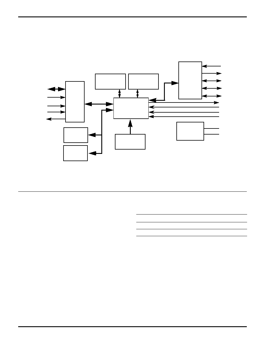
Figure 1. Z87010 Functional Block Diagram
16-Bit
I/O
Interface
/RDYE
ER//W
/EI
EA0-2
EXT 0-15
256 Word
RAM0
256 Word
RAM1
DSP
Core
Wait
State
Generator
13-Bit
Timer
CODEC
Interface
4K Words
Program ROM
RXD
TXD
SCLK
FS0
FS1
UO0-1
UI0-1
/RESET
/INT0-2
Power
VDD
VSS
Dual
Connection
Circuit
Device
Power
V
CC
V
DD
Ground
GND
V
SS

Z87010/Z87L10
Zilog
Audio Encoder/Decoders
DS96WRL0601
P R E L I M I N A R Y
2-3
2
PIN DESCRIPTION
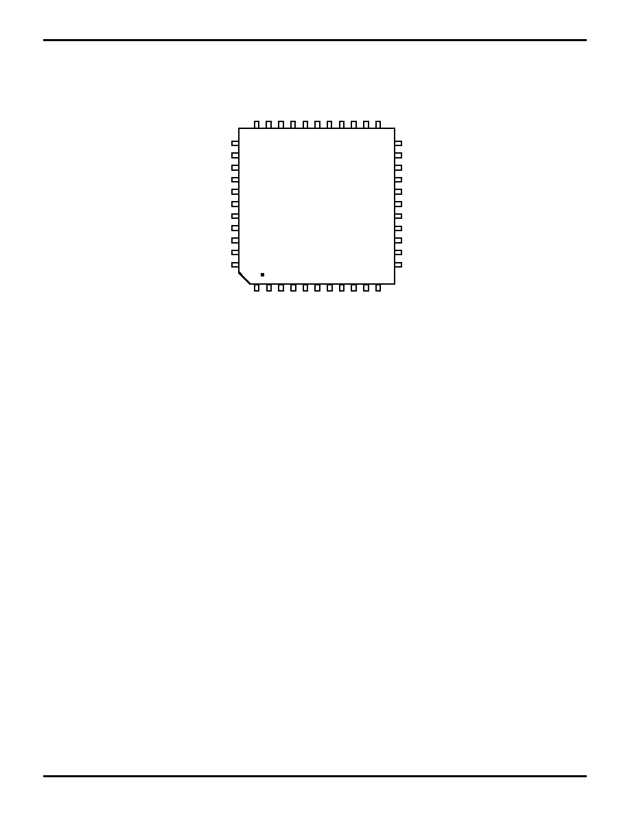
Figure 2. 44-Pin PLCC Pin Assignments
Z87010
7
17
VSS
EXT0
EXT1
EXT2
VSS
RXD
EXT12
EXT13
EXT14
VSS
EXT15
EA0
/RESET
WAIT
RD//WR
VDD
SCLK
UI0
UI1
/INT1
/INT2
EXT11
EXT3
EXT4
VSS
EXT5
EXT6
EXT7
TXD
EXT8
EXT9
VSS
EXT10
FS1
UO1
UO0
/INT
O
FSO
HAL
T
CLK
/DS
VDD
EA2
EA1
1
28
18
40
39
29
6

Z87010/Z87L10
Audio Encoder/Decoders
Zilog
2-4
P R E L I M I N A R Y
DS96WRL0601
PIN DESCRIPTION
(Continued)
Table 1. 44-Pin PLCC Pin Identification
No.
Symbol
Function
Direction
1
HALT
Stop execution
Input
2
FS0
CODEC0 frame sync
Input/Output*
3
/INT0
Interrupt
Input
4-5
UO0-UO1
User output
Output
6
FS1
CODEC1 frame sync
Input/Output*
7,11,16,20,27
V
SS
Ground
8-10
EXT0-EXT2
External data bus
Input/Output
12
RXD
Serial input from CODECs
Input
13-15
EXT12-EXT14
External data bus
Input/Output
17
EXT15
External data bus
Input/Output
18-19
EXT3-EXT4
External data bus
Input/Output
21-23
EXT5-EXT7
External data bus
Input/Output
24
TXD
Serial output to CODECs
Output
25-26
EXT8-EXT9
External data bus
Input/Output
28-29
EXT10-EXT11
External data bus
Input/Output
30
/INT2
Interrupt
Input
31
/INT1
Interrupt
Input
32
UI1
User input
Input
33
UI0
User input
Input
34
SCLK
CODEC serial clock
Input/Output*
35,42
V
DD
Power supply
Input
36
RD//WR
RD /WR strobe for EXT bus
Output
37
WAIT
WAIT state
Input
38
/RESET
Reset
Input
39-41
EA0-EA2
External address bus
Output
43
/DS
Data strobe for external bus
Output
44
CLK
Clock
Input
Note:
*Defined input or output by interface mode selection
Z87010/Z87L10
Zilog
Audio Encoder/Decoders
DS96WRL0601
P R E L I M I N A R Y
2-5
2
Figure 3. 44-Pin QFP Pin Assignments
34
44
1
23
33
Z87010
11
22
12
EXT3
EXT4
VSS
EXT5
EXT6
EXT7
TXD
EXT8
EXT9
VSS
EXT10
FS1
UO1
UO0
/INT0
FSO
HAL
T
CK
/EI
VDD
EA2
EA1
EA0
/RES
/RDYE
ER//W
VDD
SCLK
UI0
UI1
/INT1
/INT2
EXT11
VSS
EXT0
EXT1
EXT2
VSS
RXD
EXT12
EXT13
EXT14
VSS
EXT15

Z87010/Z87L10
Audio Encoder/Decoders
Zilog
2-6
P R E L I M I N A R Y
DS96WRL0601
PIN DESCRIPTION
(Continued)
Table 2. 44-Pin QFP Pin Identification
No.
Symbol
Function
Direction
1-2
EXT3-EXT4
External data bus
Input/Output
3,10
V
SS
Ground
�
4-6
EXT5-EXT7
External data bus
Input/Output
7
TXD
Serial output to CODECs
Output
8-9
EXT8-EXT9
External data bus
Input/Output
11-12
EXT10-EXT11
External data bus
Input/Output
13
/INT2
Interrupt
Input
14
/INT1
Interrupt
Input
15
UI1
User input
Input
16
UI0
User input
Input
17
SCLK
CODEC serial clock
Input/Output*
18,25
V
DD
Power supply
Input
19
ER//W
R/W for External Bus
Output
20
/RDYE
Data Ready
Input
21
/RES
Reset
Input
22-24
EA0-EA2
External Address Bus
Output
26
/EI
Data Strobe for External Bus
Output
27
CK
Clock
Input
28
HALT
Stop Execution
Input
29
FS0
CODEC0 Frame Sync
Input/Output*
30
/INT0
Interrupt
Input
31-32
U00-U01
User Output
�
33
FS1
CODEC1 Frame Sync
Input/Output*
34
V
SS
Ground
Input
35-37
EXT0-EXT2
External data bus
Input/Output
38
V
SS
Ground
Input
39
RXD
Serial Input to CODEC
Input
40-42
EXT12-EXT14
External Data Bus
Input/Output
43
V
SS
Ground
Input
44
EXT15
External Data Bus
Input/Output
Note:
*Input or output is defined by interface mode selection.
Z87010/Z87L10
Zilog
Audio Encoder/Decoders
DS96WRL0601
P R E L I M I N A R Y
2-7
2
ABSOLUTE MAXIMUM RATING
Stresses greater than those listed under Absolute Maxi-
mum Ratings may cause permanent damage to the de-
vice. This is a stress rating only; operation of the device at
any condition above those indicated in the operational sec-
tions of these specifications is not implied. Exposure to ab-
solute maximum rating conditions for extended period may
affect device reliability.
STANDARD TEST CONDITIONS
The characteristics listed below apply for standard test
conditions as noted. All voltages are referenced to ground.
Positive current flows into the referenced pin (Figure 4).
Standard test conditions are as follows:
3.0V
V
DD
3.6V (Z87L10)
4.5V
V
DD
5.5V (Z87010)
V
SS
= 0V
T
A
= -20
�
to +70
�
C
Symbol
Description
Min.
Max.
Units
V
DD
Supply Voltage
-0.3
+7.0
V
T
STG
Storage Temp
-65
�
C
+150
�
C
C
T
A
Oper. Ambient
Temp
-25
�
+70
�
C
Note:
*Voltage on all pins with respect to GND.
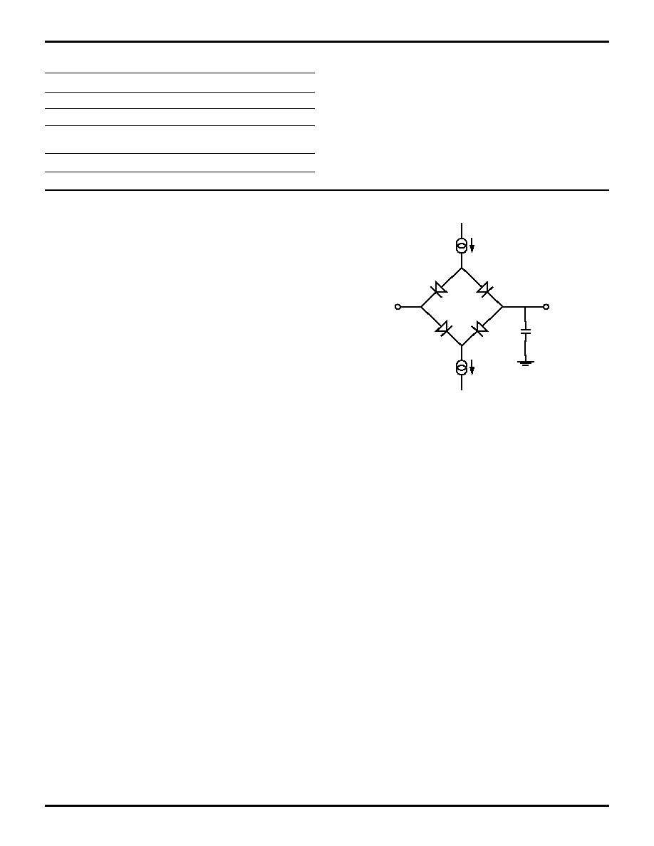
Figure 4. Test Load Diagram
Output
Under
Test
IoL
IoH
Threshold
Voltage
50pF
Z87010/Z87L10
Audio Encoder/Decoders
Zilog
2-8
P R E L I M I N A R Y
DS96WRL0601
DC ELECTRICAL CHARACTERISTICS
V
DD
= 4.5V to 5.5V (Z87010)
V
DD
= 3.0V to 3.6V (Z87L10)
T
A
=-20
�
C to +70
�
C
Symbol
Parameter
Condition
Min
Max
Units
I
DD
Supply Current
V
DD
=5.5V
fclock=16.384 MHz
40
mA
I
DC
DC Power
Consumption
V
DD
=5.5V
0.2
mA
V
IH
Input High Level
2.7
V
V
IL
Input Low Level
0.8
V
I
L
Input Leakage
10
�
A
V
OH
Output High Voltage
I
OH
=-100
�
A
V
DD
-0.2
V
V
OL
Output Low Voltage
I
OL
=2.0 mA
0.5
V (1)
I
FL
Output Floating
Leakage Current
10
�
A
Note:
5. The following specifications are pin specific: EA0-2 has I
OL
= 5 mA @ 0.5V
6. I
OH
= 1 mA @ 3.3V
T
A
=-20
�
C to +70
�
C
Symbol
Parameter
Condition
Min
Max
Units
I
DD
Supply Current
V
DD
=3.6V
fclock=16.384 MHz
25
mA
I
DC
DC Power
Consumption
V
DD
=3.6V
0.2
mA
V
IH
Input High Level
.7V
DD
V
DD
+.3
V
V
IL
Input Low Level
Vss-.3
.1V
DD
V
I
L
Input Leakage
10
�
A
V
OH
Output High Voltage
I
OH
=-50
�
A
V
DD
-0.2
V
V
OL
Output Low Voltage
I
OL
=1.0 mA
0.5
V (1)
I
FL
Output Floating
Leakage Current
10
�
A
Note:
7. The following specifications are pin specific: EA0-2 has I
OL
= 5 mA @ 0.5V
8. I
OH
= 1 mA @ 3.3V

Z87010/Z87L10
Zilog
Audio Encoder/Decoders
DS96WRL0601
P R E L I M I N A R Y
2-9
2
AC ELECTRICAL CHARACTERISTICS
)
T
A
= -20
�
C to +70
�
C
Symbol
Parameter
Min (ns)
Max (ns)
TCY
Clock Cycle Time
50
�
PWW
Clock Pulse Width
23
�
Tr
Clock Rise Time
�
2
Tf
Clock Fall Time
�
2
TEAD
EA, ER//W Delay from CK
5
28
TXVD
EXT Data Output Valid from CK
5
33
TXWH
EXT Data Output Hold from CK
3
25
TXRS
EXT Data Input Setup Time
10
�
TXRH
EXT Data Input Hold from CK
10
25
TIEDR
/EI Delay Time from CK
3
15
TIEDF
0
15
RDYS
Ready Setup Time
8
�
RDYH
Ready Hold Time
5
�
TINS
Int. Setup Time to CLK Fall
3
_
TINL
Int. Low Pulse Width
10
�
THS
Halt Setup Time to CLK Rise
3
�
THH
Halt Hold Time to CLK Rise
10
�
Z87010/Z87L10
Audio Encoder/Decoders
Zilog
2-10
P R E L I M I N A R Y
DS96WRL0601
AC TIMING DIAGRAMS
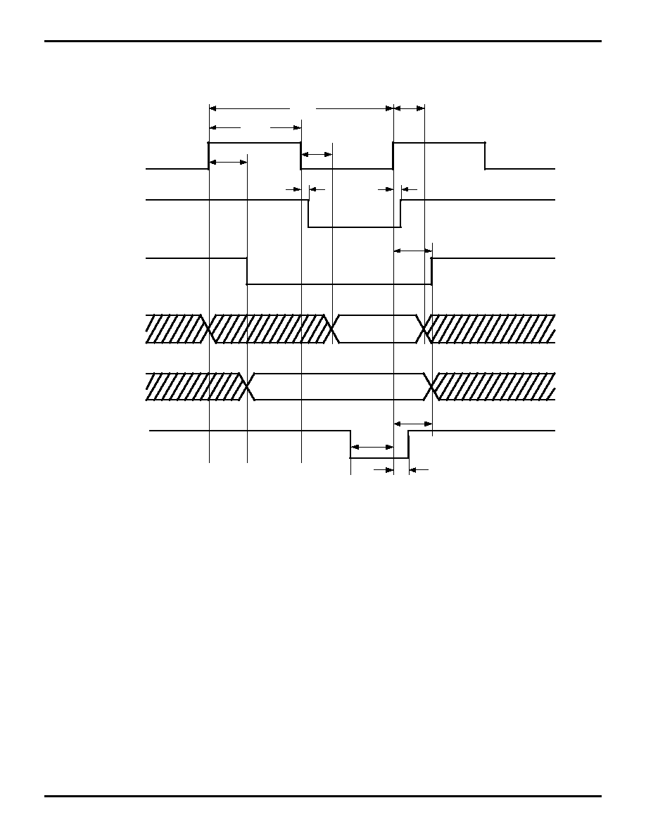
Figure 5. Write to External Device Timing
CK
/EI
ER//W
EXT (15:0)
EA (2:0)
Valid Address Out
Valid
Data Out
RDYS
/RDYE
EXT Bus:
Output
TEAD
TCY
PWW
TXWH
TXVD
TIEDF
TIEDR
TEAD
TEAD
RDYH

Z87010/Z87L10
Zilog
Audio Encoder/Decoders
DS96WRL0601
P R E L I M I N A R Y
2-11
2
Figure 6. Read From External Device Timing
CK
/EI
ER//W
EXT (15:0)
EA (2:0)
Valid Address Out
Valid
Data In
/RDYE
EXT Bus:
Input
TEAD
TCY
PWW
TXRH
TXRS
TIEDF
TIED
TEAD
RDYS
RDYH
Z87010/Z87L10
Audio Encoder/Decoders
Zilog
2-12
P R E L I M I N A R Y
DS96WRL0601
AC TIMING DIAGRAMS (Continued)
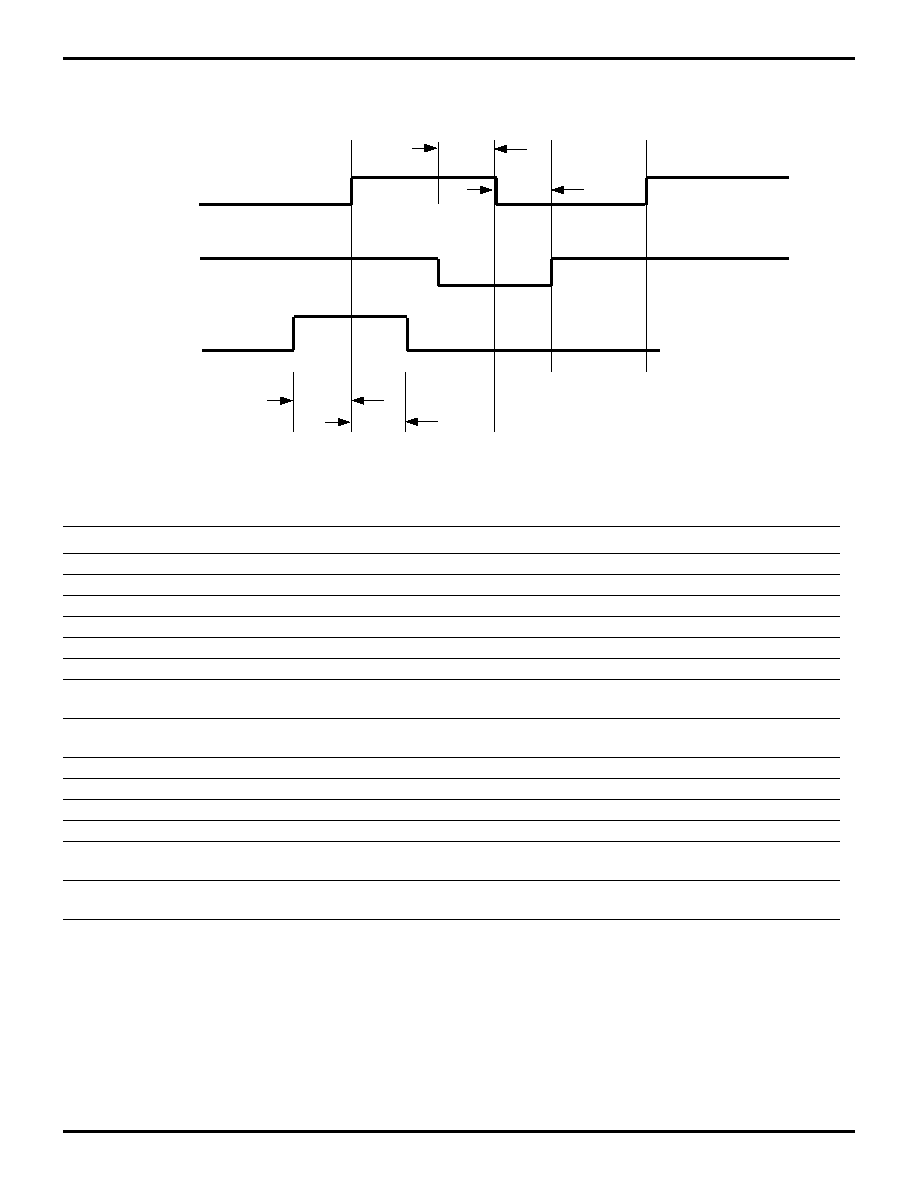
Figure 7. Interrupt/HALT Timing
Table 3. CODEC Interface-AC Timing
Internal SCLK
Min
Max
SDCR
SCLK down from CLK rise
�
15
SUCR
SCLK up from CLK rise
�
15
FDCR
FS0, FS1 down from SCLK rise
�
6
FUCR
FS0, FS1 up from SCLK rise
�
6
TDSR
TXD down from SCLK rise
�
7
TUSR
TXD up from SCLK rise
�
7
RSU
RXD Setup time in respect to
SCLK fall
7
RH
RXD Hold time in respect to
SCLK fall
0
FDCR
FS0,FS1 down from SCLK rise
�
13
FUCR
FS0, FS1 up from SCLK rise
�
13
TDSR
TXD down from SCLK rise
�
12
TUSR
TXD up from SCLK rise
�
12
RSU
RXD setup time in respect to
SCLK fall
1
RH
RXD Hold Time in respect to
SCLK fall
6
CK
Interrupt
HALT
THS
THH
TINS
TINL
Z87010/Z87L10
Zilog
Audio Encoder/Decoders
DS96WRL0601
P R E L I M I N A R Y
2-13
2
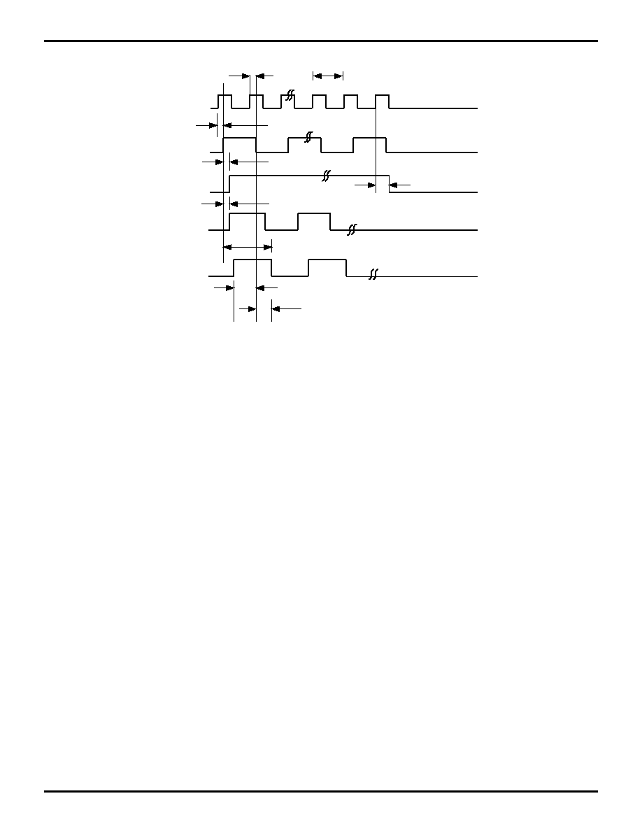
Figure 8. CODEC Interface Timing
CLOCK
SCLK
FS0, 1
TXD
RXD
SDCR
TCY
FDCR
TUSR
TDSR
RSV
RH
SUSR
FUCR

Z87010/Z87L10
Audio Encoder/Decoders
Zilog
2-14
P R E L I M I N A R Y
DS96WRL0601
PIN FUNCTIONS
CK
Clock (input). This pin controls the external clock.
EXT15-EXT0
External Data Bus (input/output). Data bus
for user-defined outside registers. The pins are normally
tri-stated, except when the outside registers are specified
as destination registers in the instructions. All the control
signals exist to allow a read or a write through this bus. The
bus is used for Z87000 interface.
ER//W
External Bus Direction (output). Data direction sig-
nal for EXT-Bus. Data is available from the CPU on
EXT15-EXT0 when this signal is Low. EXT-Bus is in input
mode (high-impedance) when this signal is High.
EA2-EA0
External Address (output). User-defined register
address output (latched). One of eight user-defined exter-
nal registers is selected by the processor with these ad-
dresses are part of the processor memory map, the pro-
cessor is simply executing internal reads and writes.
External Addresses EXT4-EXT7 are used internally by the
processor if the CODEC interface and 13-bit timer are en-
abled.
/EI
Enable Input (output). Read/Write timing signal for
EXT-Bus. User strobe is for triggering external peripheral.
Data is read by the external peripheral on the rising edge
of /EI. Data is read by the processor on the rising edge of
CK not /EI.
HALT
Halt State (input). Stop Execution Control. The CPU
continuously executes NOPs and the program counter re-
mains at the same value when this pin is held High. This
signal must be synchronized with CK. An interrupt request
must be executed (enabled) to exit HALT mode. After the
interrupt service routine, the program continues from the
instruction after the HALT.
/INT2-/INT0
Three Interrupts (input, active Low). Interrupt
request 2-0. Interrupts are generated on the rising edge of
the input signal. Interrupt vectors for the interrupt service
routine starting address are stored in the program memory
locations 0FFFH for /INT0, 0FFEH for /INT1, and 0FFFDH
for /INT2. Priorities are: INT2=Lowest, INT0=highest.
INT1 and INT2 are shared with internal Z87010 peripher-
als. INT1 is dedicated to the CODEC interface if enabled.
INT2 services the 13-bit Timer if enabled. In the Z87010
standard software configuration, INT0 and INT2 are not
used; INT1 is used by the CODEC interface.
/RES
Reset (input, active Low). This pin controls the asyn-
chronous reset signal. The /RESET signal must be kept
Low for at least one clock cycle. The CPU pushes the con-
tents of the Program Counter (PC) onto the stack and then
fetches a new PC value from program memory address
0FFCH after the reset signal is released.
/RDYE
Data Ready (input). User-supplied Data Ready sig-
nal for data to and from external data bus. This pin stretch-
es the /EI and ER//W lines and maintains data on the ad-
dress bus and data bus. The ready signal is sampled from
the rising clock only if ready is active. A single wait-state
can be generated internally by setting the appropriate bits
in the EXT7-2 register.
UI1-UI0
Two Input Pins (input). General-purpose input
pins. These input pins are directly tested by the conditional
branch instructions: and are reflected in two bits of the sta-
tus register (S10 and S11). These are asynchronous input
signals that have no special clock synchronization require-
ments.
U01-U00
Two Output Pins (push-pull output). General-
purpose output pins. These pins reflect the value of two
bits in the status register (S5 and S6). UO0 is dedicated to
provide an interrupt signal to the Z87000 controller. Note:
the user output pin values are the inverse of the status reg-
ister content.

Z87010/Z87L10
Zilog
Audio Encoder/Decoders
DS96WRL0601
P R E L I M I N A R Y
2-15
2
FUNCTIONAL DESCRIPTION
General functional partitioning of the Z87010 is shown in
Figure 1. The chip consists of the Z89S00 static DSP core
with 512 words of RAM, 4K words of ROM, a CODEC in-
terface, a general-purpose timer and a wait state genera-
tor.
The DSP core is characterized by an efficient hardware ar-
chitecture that allows fast arithmetic operations such as
multiplication, addition, subtraction and multiply-accumu-
late of two 16-bit operands. Most instructions are executed
in one clock cycle.
The DSP core uses a RAM memory of 512 16-bit words di-
vided in two banks.
Program Memory. The Z87010 has a 4K 16-bit words in-
ternal ROM including 4 words for interrupt and reset vec-
tors. The ROM is mapped at address 0000H to 0FFFH.
The reset vector is located at address 0FFCH, interrupts
INT0 is at 0FFDH, interrupt INT1 is at 0FFEH and interrupt
INT2 is at 0FFFH.
Interrupts. The Z87010 has three positive edge-triggered
interrupt inputs pins. However, INT1 is dedicated to the
CODEC interface and INT2 is dedicated to the 13-bit timer
if these peripherals are enabled.
User Inputs. The Z87010 has two inputs, UI0 and UI1,
which may be used by Jump and Call instructions. The
Jump or Call tests one of these pins and if appropriate,
jumps to a new location. Otherwise, the instruction be-
haves like a NOP. These inputs are also connected to the
status register bits S10 and S11, which may be read by the
appropriate instruction.
User Outputs. The status register bits S5 and S6 connect
directly to UO0 and UO1 pins and may be written to by the
appropriate instruction. Note: The user output value is the
opposite of the status register content.
I/O Bus. The Z87010 provides a 16-bit, CMOS compatible
I/O bus. I/O Control pins provide convenient communica-
tion capabilities with external peripherals. Single cycle ac-
cess is possible. For slower communications, an on-board
hardware wait-state generator can be used to accommo-
date timing conflicts.
These latched output address pins (EA0-2) allow a maxi-
mum of eight external peripherals. However up to four of
these addresses (EXT4-7) are used by internal peripherals
if enabled.
EXT4
13-bit Timer Configuration Register
EXT5
CODEC Interface Channel 0 Data
EXT6
CODEC Interface Channel 1 Data
EXT7
CODEC Interface Configuration Register and Wait
State Generator.

Z87010/Z87L10
Audio Encoder/Decoders
Zilog
2-16
P R E L I M I N A R Y
DS96WRL0601
CODEC INTERFACE
The CODEC interface provides direct-connect capabilities
for standard 8-bit PCM CODECs with hardware
�
-law
compression. Internal registers EXT5, EXT6 and EXT7 are
used to program the CODEC mode. One serial clock and
two frame sync control signals are provided, allowing for
two bidirectional data channels.
Note:
�
-law expansion must be done in software.
CODEC Interface Hardware
The Hardware for the CODEC Interface uses six 16-bit
registers,
�
-law compression logic and general-purpose
logic to control transfers to the appropriate register.
CODEC Interface Control Signals
SCLK (Serial Clock)
The Serial Clock provides a clock signal for operating the
external CODEC. A 4-bit prescaler is used to determine
the frequency of the output signal.
SCLK = (0.5* CLK)/PS where: CLK = System Clock
PS = 4-bit Prescaler*
Note: An internal divide-by-two is performed before the
clock signal is passed to the Serial Clock prescaler.
* The Prescaler is an up-counter.
Figure 9. CODEC Interface Block Diagram
�
-Law
Compression
Data Bus
16
16
16
16
16
16
CLKIN
TXD
EXT5-2
CLKIN
CLKIN
CLKIN
CLKIN
EXT5-1
EXT6-1
EXT6-2
CONTROL
LOGIC
RXD
EXT7-1
EXT7-2
16
Z87010/Z87L10
Zilog
Audio Encoder/Decoders
DS96WRL0601
P R E L I M I N A R Y
2-17
2
Assuming an input clock of 16.384 MHz, SCLK is pro-
grammed by the Z87010 embedded software for 2.048
MHz.
TXD (Serial Output to CODEC)
The TXD line provides 8-bit data transfers. Each bit is
clocked out of the processor by the rising edge of the
SCLK, with the MSB transmitted first.
RXD (Serial Input from CODEC)
The RXD line provides 8-bit data transfers. Each bit is
clocked into the processor by the falling edge of the SCLK,
with the MSB received first.
FS0, FS1 (Frame Sync)
The Frame Sync is used for enabling data transfer/receive.
The rising and falling edge of the Frame Sync encloses the
serial data transmission. The Z87010 embedded software
programs the Frame Sync signal to 8 kHz.
Interrupt
Once the transmission of serial data is completed an inter-
nal interrupt signal is initiated. A single-cycle Low pulse
provides an interrupt on INT1. When this occurs, the pro-
cessor will jump to the defined Interrupt 1 vector location.
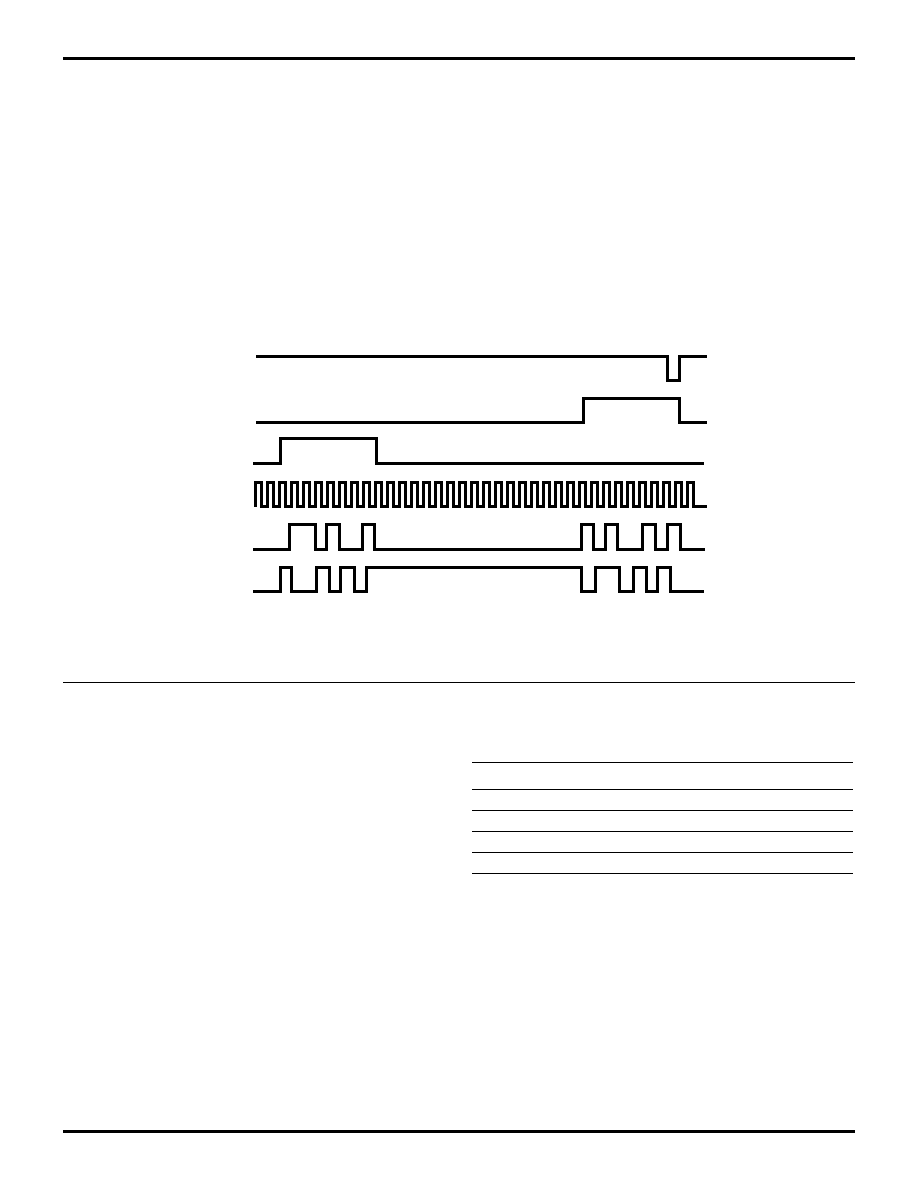
CODEC Interface Timing
Figure 10 depicts a typical 8-bit serial data transfer using
both of the CODEC Interface Channels. The transmitting
data is clocked out on the rising edge of the SCLK signal.
An external CODEC clocks data in on the falling edge of
the SCLK signal. Once the serial data is transmitted, an in-
terrupt is given. The CODEC interface signals are not initi-
ated if the CODEC interface is not enabled.
The following modes are available for FSYNC and SCLK
signals:
Figure 10. CODEC Interface Timing (8-Bit Mode)
/int1
fs1
sclk
fs0
txd
rxd
SCLK
FSYNC
Internal
Internal
External
External
External
Internal
Internal
External
Z87010/Z87L10
Audio Encoder/Decoders
Zilog
2-18
P R E L I M I N A R Y
DS96WRL0601
CODEC INTERFACE (Continued)
The CODEC interface timing is independent of the proces-
sor clock when external mode is chosen. This feature pro-
vides the capability for an external device to control the
transfer of data to the Z87010. The Frame Sync signal en-
velopes the transmitted data (Figure 10), therefore care
must be taken to ensure proper sync signal timing. In the
cordless phone system, the SCLK is externally provided
by the Z87000 controller, while FSYNC is internally gener-
ated.
The Transmit and Receive lines are used for transfer of se-
rial data to or from the CODEC interface. The CODEC in-
terface performs both data transmit and receive simulta-
neously.
The FSYNC Signals (FS0, FS1) when programmed for in-
ternal mode, are generated by 9-bit counter with SCLK as
input clock. Together with the SCLK prescaler, this counter
forms a 13-bit counter clocked by the system clock divided
by two. The output of this counter can be used to clock the
general-purpose 13-bit counter/timer, to form a 26-bit
counter.
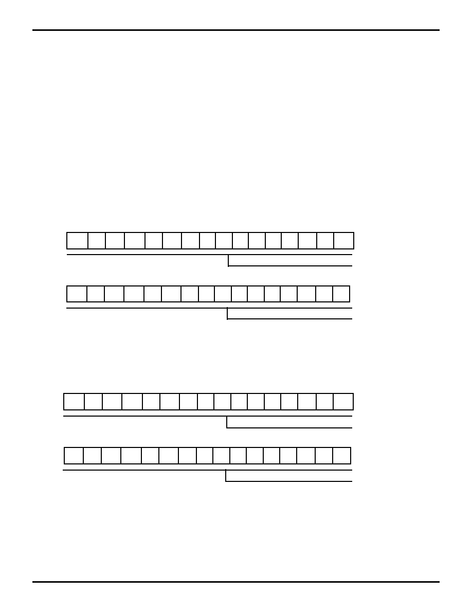
CODEC Control Registers
The CODEC interface is accessed through addresses
EXT5, EXT6 and EXT7. The data accesses are double-
buffered registers: two registers (EXT5-1 and EXT5-2) are
mapped on address EXT5 and similarly EXT6-1 and
EXT6-2 registers are mapped on address EXT6.
Figure 11. CODEC Interface Data Registers (Channel 0)
D15 D14 D13
D11 D10 D9 D8
D12
D7 D6 D5 D4 D3 D2
D1
D0
EXT5-1
Data Bits 15-0
D15 D14 D13
D11 D10 D9 D8
D12
D7 D6 D5 D4 D3 D2
D1 D0
EXT5-2
Data Bits 15-0
Figure 12. CODEC Interface Data Registers (Channel 1)
D15 D14 D13
D11 D10 D9 D8
D12
D7 D6 D5 D4 D3 D2
D1 D0
EXT6-1
Data Bits 15-0
D15 D14 D13
D11 D10 D9 D8
D12
D7 D6 D5 D4 D3 D2
D1 D0
EXT6-2
Data Bits 15-0

Z87010/Z87L10
Zilog
Audio Encoder/Decoders
DS96WRL0601
P R E L I M I N A R Y
2-19
2
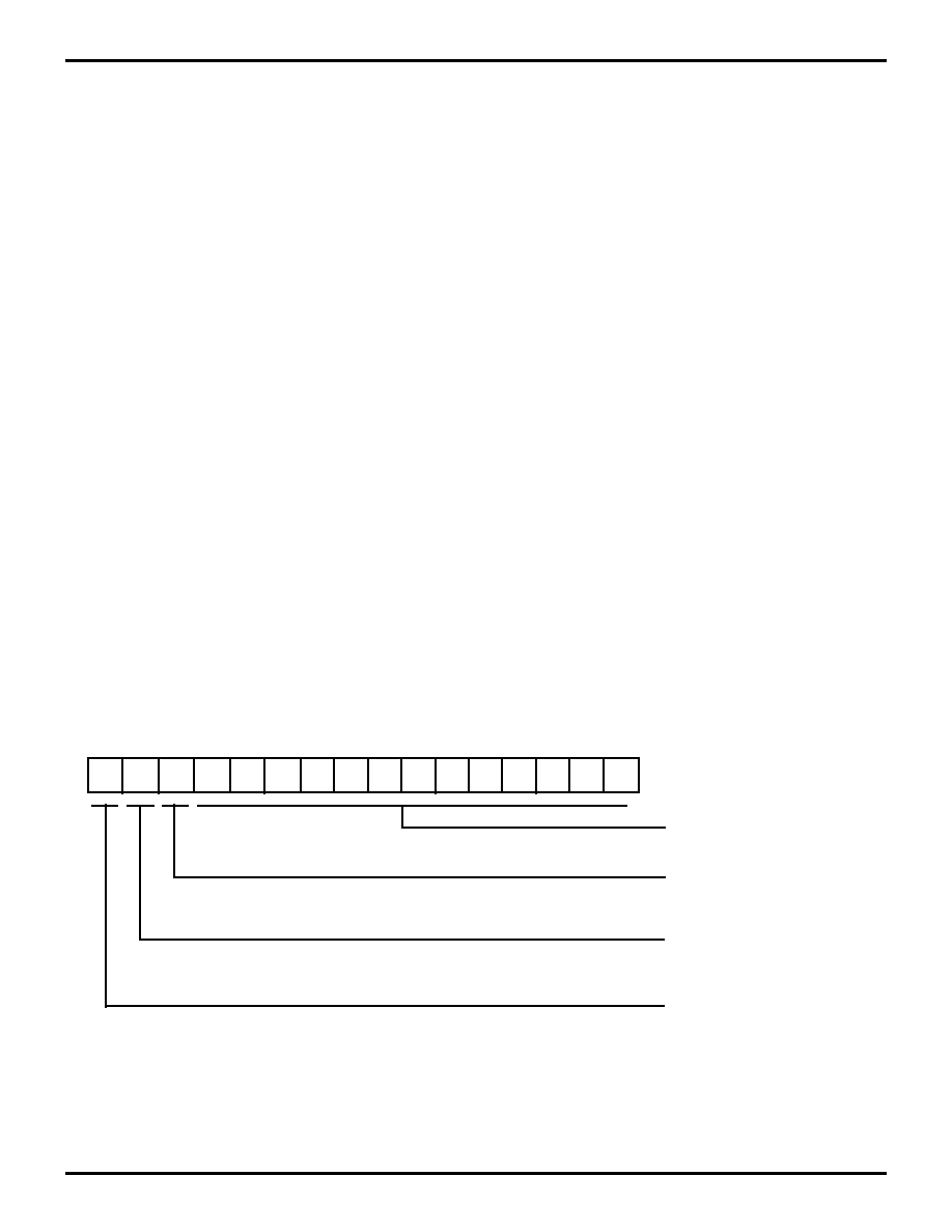
Figure 13. CODEC Interface Control Register
D7
D6
D5
D4
D3
D2
D1
D0
D15
D14
D13
D12
D11
D10
D9
D8
SCLK Prescaler (up-counter)
EXT7-1
SCLK/FSYNC Ratio Prescaler (up-counter)
CODEC Mode
01 Reserved
10 Reserved
11 Reserved
FSYNC
0 External Source*
1 Internal Source
CODEC 0 Disable/Enable
0 = Disable*
1 = Enable
Note: The timer is an up-counter.
Example: EXT7-1 = #%x00D OSC = 12.288 MHz, SCLK = 2.048 MHz, FSYNC = 8 kHz
EXT7-1 = #%x80F OSC = 12.288 MHz, SCLK = 6.144 MHz, FSYNC = 48 kHz
EXT7-1 = #%xFFx No interrupt
EXT7-1 = #%x000 Max interrupt period (667
�
s for OSC = 12.288 MHz)
* Default
Figure 14. Wait/State/CODEC Interface Control Register
D7
D6
D5
D4
D3
D2
D1
D0
D15
D14
D13
D12
D11
D10
D9
D8
EXT7-2
Wait State EXT0
Wait State EXT1
Wait State EXT2
Wait State EXT3
Wait State EXT4
Wait State EXT5
Wait State EXT6
SCLK
0 External Source*
1 Internal Source
CODEC 1 Disable/Enable
0 = Disable*
1 = Enable
nws - no wait states
ws - one wait states
00 no wait states (nws)
01 read (nws), write (ws)
10 read (ws), write (nws)
11 read (ws), write (ws)
*Default
Z87010/Z87L10
Audio Encoder/Decoders
Zilog
2-20
P R E L I M I N A R Y
DS96WRL0601
CODEC INTERFACE (Continued)
The CODEC Interface Control Register (EXT7-1) is shown
on Figure 13. Setting of the CODEC mode, FSYNC mode
and CODEC 0 enable/disable is done through this register.
A second control register (EXT7-2) also mapped on ad-
dress EXT7 control the CODEC 1, SCLK source and wait
state generator (see Figure 9). The "operation" section de-
scribes how to access the various register.
Wait-State Generator
An internal wait state generator is provided to accommo-
date slow external peripherals. One wait-state can be au-
tomatically inserted by the Z87010 in any EXT bus access.
Read and/or write cycles can be independently lengthened
for each register, by setting register EXT7-2 accordingly.
See Figure 9 for detailed description of EXT7-2.
The Z87010 software uses one wait state on all external
register accesses.
For additional wait states, a dedicate pin (/RDYE) can be
held high. The /RDYE pin is monitored only during execu-
tion of a Read or Write Instruction to external peripherals.
General-Purpose Counter Timer
A 13-bit counter/timer is available for general-purpose use.
When the counter counts down to the zero state, an inter-
rupt is received on INT2. If the counter is disabled, EXT4
can be used as a general-purpose address. The counting
operation of the counter can be disabled by resetting bit
14. By selecting the clock source to the CODEC counter
output (FSYNC), one can extend the counter to a total of
26 bits.
Note: Placing zeroes into the Count Value register does
not generate an interrupt. Therefore it is possible to have
a single-pass option by loading the counter with zero after
the start of count.
The Counter is defaulted to the Enable state. If the system
designer does not choose to use the timer, the counter can
be disabled. Once disabled, the designer cannot enable
the counter unless a reset of the processor is performed.
Example:
LD
EXT, #%C0008 1100 0000 0000 1000
; Enable Counter
; Enable Counting
; Clock Source = OSC/2
; Count Value = 1000=8
; Interrupt will occur every 16 clock
cycles
Figure 15. Timer Register
D7
D6
D5
D4
D3
D2
D1
D0
D15
D14
D13
D12
D11
D10
D9
D8
EXT4
Count Value (Down-Counter)
Clock Source
Count Operation
Counter
0 Oscillator/2*
1 CODEC Counter Output
0 = Disable*
1 = Enable
0 = Disable
1 = Enable*
* Default State
Z87010/Z87L10
Zilog
Audio Encoder/Decoders
DS96WRL0601
P R E L I M I N A R Y
2-21
2
OPERATION
Disabling Peripherals
Disabling a properly (CODEC Interface, Counter) provides
a general-purpose use of the EXT address pertaining to
the specific peripheral. If the peripheral is not disabled, the
EXT control signals and EXT data are still provided but
transfer of data on the EXT pins is not available (since in-
ternal transfers are being processes on the internal bus).
Care must be taken to ensure that control of the EXT bus
does not provide bus conflicts.
Accessing the CODEC Interface Registers
EXT5, EXT6 AND EXT7 host double buffered registers.
External serial CODEC data is transferred from pin RxD to
the Z87010 CODEC interface registers EXT5-2. At the
same time, the data present in EXT5-2 is serially trans-
ferred to the external CODEC through pin TxD.
Writing a new data word to EXT5 loads that data word to
EXT5-2 and transfers the current contents of EXT5-2 to
EXT5-1. Reading data from EXT5 reads the contents of
EXT5-1. Core must be taken to ensure that EXT5 is not
written to while the serial CODEC transfer is taking place.
This is achieved by only writing to EXT5 after the CODEC
interrupt. This also transfers the CODEC value to EXT5-1
which can be read in software.
The correct succession of operations is thus
1. Wait for Interrupt
2. Write to EXT5
3. Read from EXT5
The same discussion applies for EXT6.
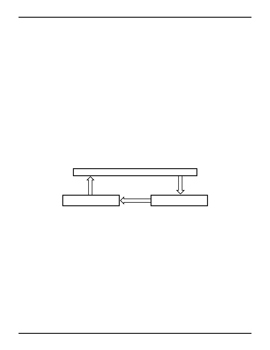
A similar hardware architecture is used for EXT7. Writing
to EXT7 loads the register EXT7-2 and transfers the previ-
ous contents of EXT7-2 to EXT7-1. Reading from EXT7 re-
turns the contents of EXT7-1.
In order to load both registers, two successive load opera-
tions to EXT7 are required: first with the contents of EXT7-
1 then with the contents of EXT7-2. (See Figure 16).
Figure 16. EXT7 Register Configuration
Internal 16-Bit Bus
Wait-State Register
16
EXT7-1
EXT7-2
16
CODEC Timer Register
EXT7-1
EXT7-2