 | –≠–ª–µ–∫—Ç—Ä–æ–Ω–Ω—ã–π –∫–æ–º–ø–æ–Ω–µ–Ω—Ç: Z87100 | –°–∫–∞—á–∞—Ç—å:  PDF PDF  ZIP ZIP |

DS96WRL0700
P R E L I M I N A R Y
3-1
3
P
RELIMINARY
P
RODUCT
S
PECIFICATION
Z87100
3
PN M
ODULATOR
W
IRELESS
T
RANSMITTER
FEATURES
s
3.0V to 5.5V Operating Range
s
On-Chip PN Modulator for Spread Spectrum
Communications
s
ROM-Programmable PN Codes, up to 256 Bits ("Chips")
s
Fast Instruction Pointer - 1.0
µ
s @ 12 MHz
s
Two Standby Modes - STOP and HALT
s
12 Input/Output Lines (One with Comparator Input)
s
Two Programmable 8-Bit Counter/Timers
s
6-Bit Programmable Prescaler
s
Six Vectored, Priority Interrupts (Two External, One
Software Generated)
s
Maximum Clock Speed of 12 MHz
s
Watch-Dog/Power-On Reset Timer
s
Analog Comparator with Programmable Interrupt
Polarity
s
On-Chip Oscillator that Accepts a RC, or External Clock
Drive
s
Low EMI Noise Mode
s
0
∞
to +70
∞
C Ultra-Low Power Operation at 10 kHz
GENERAL DESCRIPTION
The Z87100 Wireless Controller is a member of the Z8
Æ
single-chip microcontroller family and is manufactured in
CMOS technology. Zilog's CMOS Z87100 microcontroller
offers fast execution, efficient use of memory, sophisticat-
ed interrupts, input/output bit manipulation capabilities,
and easy hardware/software system expansion along with
low cost and low power consumption.
The Z87100 architecture is based on Zilog's 8-bit micro-
controller core with the addition of an Expanded Register
File which allows access to register mapped peripheral
and I/O circuits. The Z87100 offers a flexible I/O scheme
and a number of ancillary features that are useful in many
consumer, industrial, automotive, and advanced scientific
applications.
The Z87100 is designed with specific features for wireless
spread spectrum applications using direct sequence pseu-
do-noise (PN) modulation. With up to 256 bits ("chips") of
specially designated "PN ROM", one or more PN code se-
quences may be stored and used to PN-modulate data
generated by the Z87100. PN modulation is synchronous
with the data, using an integer number of PN chips per data
bit.
The Z87100 features an Internal Time Base Counter which
provides a real time clock for Stop-Mode Recovery or inter-
rupt at programmable intervals of 0.25 seconds, one sec-
ond, one minute and one hour. This requires an external
clock oscillator signal at 32.768 kHz.
Special PN modulator control registers allow the user to
select the desired PN modulator outputs, to choose the PN
clock source and PN sequence start address in PN ROM,
to stop/start and enable/disable the PN modulator, and to
determine whether a complete PN code sequence is mod-
ulated against a single bit or an integer fraction or multiple
of a single bit. The PN-modulated data may then be used
Part
ROM
(Kbytes)
RAM*
(Bytes)
Package
Information
Z87100
1
124
18-pin DIP & SOIC
Note:
*General-Purpose
Z87100
Wireless Transmitter
Zilog
3-2
P R E L I M I N A R Y
DS96WRL0700
GENERAL DESCRIPTION
(Continued)
with an external modulator and RF section to form a com-
plete wireless spread spectrum transmitter.
The device's many applications demand powerful I/O ca-
pabilities. The Wireless Controller fulfills this with 12 pins
dedicated to input and output. These lines are grouped into
two ports, and are configurable under software control to
provide timing, status signals, or parallel I/O.
Three basic address spaces are available to support this
wide range of configurations; Program Memory, Register
File, and Expanded Register File. The Register File is
composed of 124 bytes of General-Purpose Registers, two
I/O Port registers and fifteen Control and Status registers.
The Expanded Register File consists of two port registers,
four control registers and six PN modulator registers.
With powerful peripheral features such as on-board com-
parators, counter/timers, Watch-Dog Timer, and PN mod-
ulator, the Z87100 meets the needs for most sophisticated
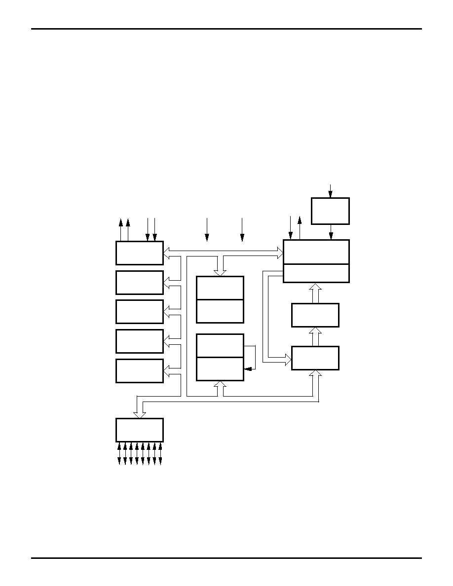
wireless and low-power controller applications (Figure 1).
Figure 1. Functional Block Diagram
Port 3
Counter/
Timers (2)
Interrupt
Control
Analog
Comparator
Port 2
I/O
(Bit Programmable)
ALU
FLAG
Register
Pointer
Register File
144 x 8-Bit
VCC
GND
Input
Output
PN
Modulator
Prg. Memory
1024 x 8-Bit
Program
Counter
Time Base
Generator
RC
Machine Timing &
Instruction Control
WDT, POR
TMBASE
Z87100
Zilog
Wireless Transmitter
DS96WRL0700
P R E L I M I N A R Y
3-3
3
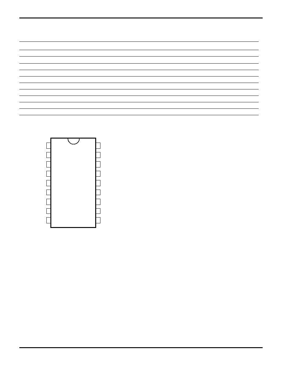
PIN DESCRIPTION
Table 1. 18-Pin DIP/SOIC Pin Identification
No
Symbol
Function
Direction
1-4
P24-27
Port 2, Pins 4, 5, 6, 7
In/Output
5
V
CC
Power Supply
Input
6
RC2
RC Oscillator Clock
Output
7
RC1
RC Oscillator Clock
Input
8-9
P31, P33
Port 3, Pins 1, 3
Fixed Input
10
TMBASE
Time Base Clock
Input
11
GND
Ground
Input
12-13
P35-36
Port 3, Pins 5, 6
Fixed Output
14
GND
Ground Input
15-18
P20-23
Port 2, Pins 0, 1, 2, 3
In/Output
Figure 2. 18-Pin DIP/SOIC Pin Configuration
1
2
9
3
4
5
6
7
8
18
17
16
15
14
13
12
11
10
P23
P22
TMBASE
P21
P20
GND
P36
P35
GND
P24
P25
P33
P26
P27
VCC
RC2
RC1
P31
Z87100
Z87100
Wireless Transmitter
Zilog
3-4
P R E L I M I N A R Y
DS96WRL0700
ABSOLUTE MAXIMUM RATING
Stresses greater than those listed under Absolute Maxi-
mum Ratings may cause permanent damage to the de-
vice. This is a stress rating only; operation of the device at
any condition above those indicated in the operational sec-
tions of these specifications is not implied. Exposure to ab-
solute maximum rating conditions for extended period may
affect device reliability.
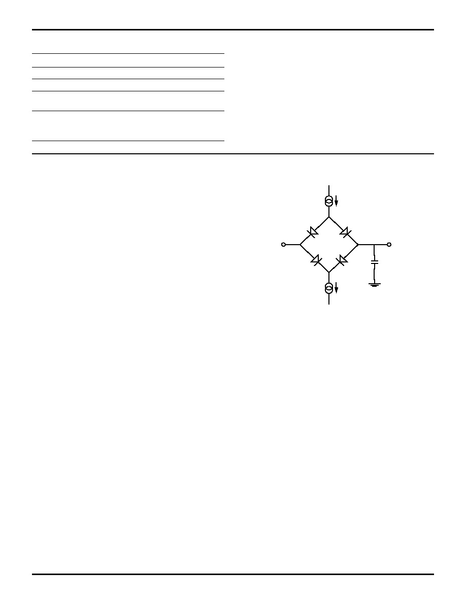
STANDARD TEST CONDITIONS
The characteristics listed below apply for standard test
conditions as noted. All voltages are referenced to ground.
Positive current flows into the referenced pin (Figure 3).
Sym
Description
Min
Max
Units
V
CC
Supply Voltage*
≠0.3
+7.0
V
T
STG
Storage Temp
≠65
+150
C
T
A
Oper Ambient
Temp
C
Notes:
1. *Voltage on all pins with respect to GND.
2. See Ordering Information
Figure 3. Test Load Configuration
Output
Under
Test
IoL
IoH
Threshold
Voltage
50pF

Z87100
Zilog
Wireless Transmitter
DS96WRL0700
P R E L I M I N A R Y
3-5
3
DC ELECTRICAL CHARACTERISTICS
T
A
= 0
∞
C to +70
∞
C
Typical
Sym
Parameter
V
CC
Min
Max
@ 25
∞
C
Units
Conditions
Notes
Max Input
Voltage
3.0V
5.5V
12
12
V
V
I
IN
250
µ
A
I
IN
250
µ
A
V
CH
Clock Input
High Voltage
3.0V
5.5V
0.9 V
CC
0.9 V
CC
V
CC
+0.3
V
CC
+0.3
2.4
3.9
V
V
Driven by External Clock
Generator
V
CL
Clock Input
Low Voltage
3.0V
5.5V
V
SS
≠0.3
V
SS
≠0.3
0.2 V
CC
0.2 V
CC
1.6
2.7
V
V
Driven by External Clock
Generator
V
IH
Input High
Voltage
3.0V
5.5V
0.7 V
CC
0.7 V
CC
V
CC
+0.3
V
CC
+0.3
1.8
2.8
V
V
V
IL
Input Low
Voltage
3.0V
5.5V
V
SS
≠0.3
V
SS
≠0.3
0.2 V
CC
0.2 V
CC
1.0
1.5
V
V
V
OH
Output High
Voltage
3.0V
5.5V
V
CC
≠0.4
V
CC
≠0.4
3.1
4.8
V
V
I
OH
= ≠2.0 mA
I
OH
= ≠2.0 mA
V
OL1
Output Low
Voltage
3.0V
5.5V
0.8
0.4
0.2
0.1
V
V
I
OL
=+4.0 mA
I
OL
=+4.0 mA
V
OL2
Output Low
Voltage
3.0V
5.5V
1.0
1.0
0.4
0.5
V
V
I
OL
= 6 mA, 3 Pin Max
I
O
= +12 mA, 3 Pin Max
V
OFFSET
Comparator
Input Offset
Voltage
3.0V
5.5V
25
25
10
10
mV
mV
I
IL
Input Leakage
(Input bias
current of
comparator)
3.0V
5.5V
≠1.0
≠1.0
1.0
1.0
µ
A
µ
A
V
IN
= O
V
, V
CC
V
IN
= O
V
, V
CC

Z87100
Wireless Transmitter
Zilog
3-6
P R E L I M I N A R Y
DS96WRL0700
DC ELECTRICAL CHARACTERISTICS (Continued)
I
OL
Output
Leakage
3.0V
5.5V
≠1.0
≠1.0
1.0
1.0
µ
A
µ
A
V
IN
= O
V
, V
CC
V
IN
= O
V
, V
CC
I
CC
Supply Current 3.0V
5.5V
4.5V
8.0
15
15
4.5
9.0
10
mA
mA
µ
A
@ 12 MHz
@ 12 MHz
10 kHz; external RC
2,3
2,3
2,3
I
CC1
Standby
Current
(HALT mode)
3.0V
5.5V
4.5
7.0
2.0
4.0
mA
mA
HALT mode V
IN
=0
V
, V
CC
@12 MHz
HALT mode V
IN
=0V,
V
CC
@ 12 MHz
2,3
2,3
3.0V
5.5V
2.0
4.5
1.0
2.5
mA
mA
Clock Divide-by-16
@12 MHz
Clock Divide-by-16
@ 12 MHz
2,3
2,3
I
CC2
Standby
Current
(STOP mode)
3.0V
5.5V
10
10
1.0
3.0
µ
A
µ
A
STOP mode V
IN
= O
V
,
V
CC
WDT is not Running
STOP mode V
IN
= O
V
,
V
CC
WDT is not Running
4,7
4,7
3.0V
5.5V
TBD
TBD
160
200
µ
A
µ
A
STOP mode V
IN
= O
V
,
V
CC
WDT is Running
STOP mode V
IN
= O
V
,
V
CC
WDT is Running
4,7
4,7
5.5V
12
5
µ
A
STOP mode;
TMBASE=32.768 kHz;
WDT is not Running
6,7
T
POR
Power-On
Reset
3.0V
5.5V
7
3
24
13
13
7
ms
ms
V
LV
V
CC
Low
Voltage
1.50
2.65
2.1
V
2 MHz max Ext. CLK
Freq.
1
Notes:
1. V
LV
increases as the temperature decreases.
2. All outputs unloaded, I/O pins floating,
inputs at either rail, TMBASE clock input grounded.
3. C
L1
= C
L2
= 100 pF
4. Same as note 2 except inputs at V
CC
.
5. Low EMI oscillator selected; SCLK = RC1/2;
10 kHz external oscillator with the comparator not enabled 10
µ
A.
10 kHz external oscillator with the comparator enabled 310
µ
A
RC selected for WDT; 10 kHz RC oscillator
(corresponding to R = 1.2M
C~ 68 pF), comparator is off.
6. Z8 in STOP moderate off; Z8 in STOP mode; WDT off.
TMBASE selected; as Z8 system clock source
Time base counter enabled; V
CC
= 5.5V.
7. Analog Comparator disabled
T
A
= 0
∞
C to +70
∞
C
Typical
Sym
Parameter
V
CC
Min
Max
@ 25
∞
C
Units
Conditions
Notes
Z87100
Zilog
Wireless Transmitter
DS96WRL0700
P R E L I M I N A R Y
3-7
3
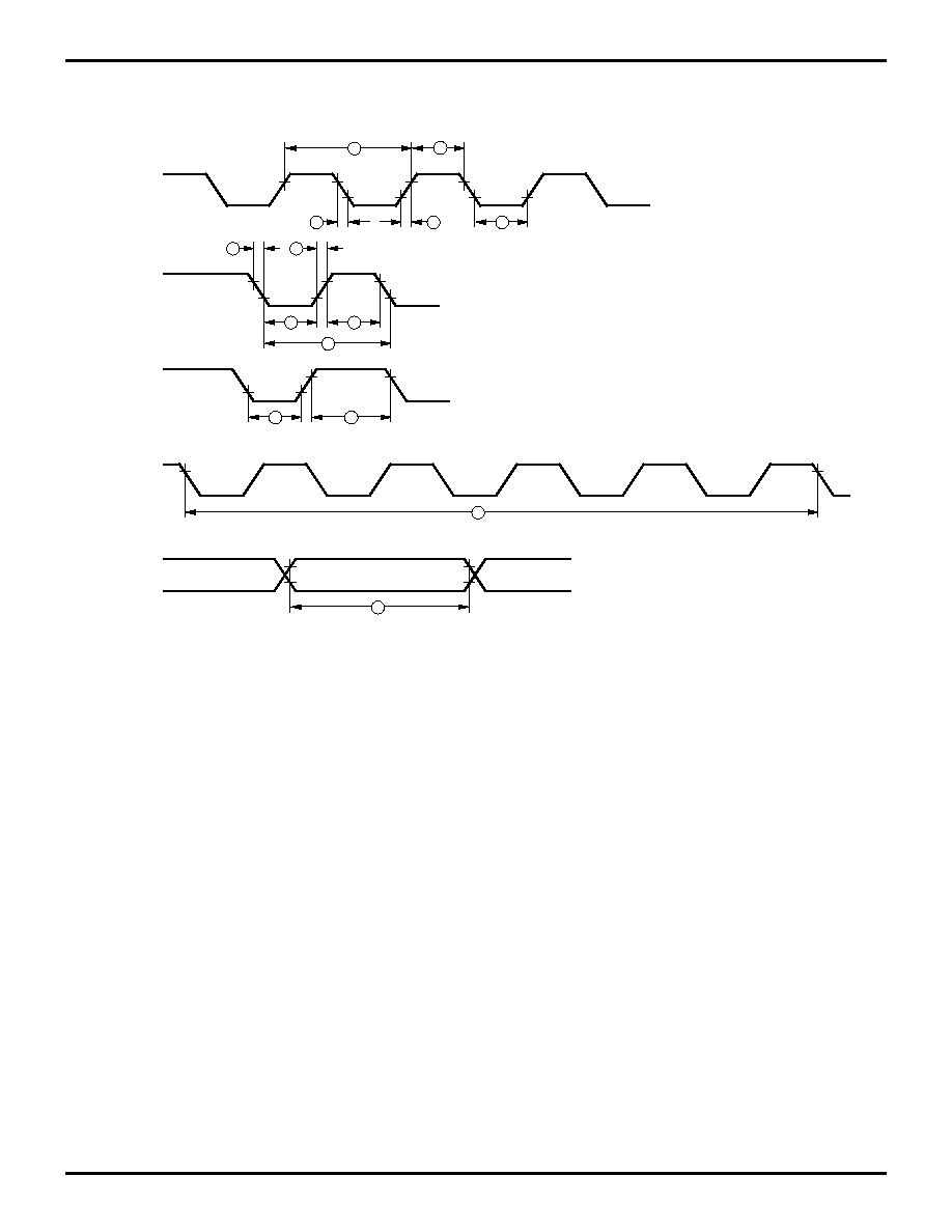
AC ELECTRICAL CHARACTERISTICS
Figure 4. Additional Timing
Clock
1
3
4
8
2
2
3
TIN
IRQN
6
5
7
7
11
Clock
Setup
10
9
Stop-Mode
Recovery
Source

Z87100
Wireless Transmitter
Zilog
3-8
P R E L I M I N A R Y
DS96WRL0700
AC ELECTRICAL CHARACTERISTICS
T
A
=0
∞
C to +70
∞
C
12 MHz
No
Sym
Parameter
V
CC
Min
Max
Units
Notes
1
TpC
Input Clock Period
3.3V
5.0V
83
83
100,000
100,000
ns
ns
1
1
2
TrC,TfC
Clock Input Rise
and Fall Times
3.3V
5.0V
15
15
ns
ns
1
1
3
TwC
Input Clock Width
3.3V
5.0V
26
26
ns
ns
1
1
4
TwTinL
Timer Input
Low Width
3.3V
5.0V
100
70
ns
ns
1
1
5
TwTinH
Timer Input
High Width
3.3V
5.0V
3TpC
3TpC
1
1
6
TpTi
Timer Input Period
3.3V
5.0V
8TpC
8TpC
1
1
7
TrTin,
TtTin
Timer Input Rise
and Fall Timer
3.3V
5.0V
100
100
ns
ns
1
1
8
TwIL
Int. Request
Low Time
3.3V
5.0V
100
70
ns
ns
1,2
1,2
9
TwIH
Int. Request High
Time
3.3V
5.0V
3TpC
3TpC
1,2
1,2
10
Twsm
Stop-Mode
Recovery
Width Spec
3.3V
5.0V
12
12
ns
ns
11
Tost
RC Oscillator
Start-up Time
3.3V
5.0V
5TpC
5TpC
ms
ms
Reg.4
Twdt
Watch-Dog Timer
Refresh Time
3.3V
5.0V
15
5
ms
ms
D0=0 5
D1=05
3.3V
5.0V
30
16
ms
ms
D0=15
D1=05
3.3V
5.0V
60
25
ms
ms
D0=05
D1=15
3.3V
5.0V
250
120
ms
ms
D0=15
D1=15
Notes:
1. Timing Reference uses 0.9 V
CC
for a logic 1 and 0.1 V
CC
for a logic 0.
2. Interrupt request through Port 3 (P33-P31)
3. 5.0V
±
0.5V, 3.3V
±
0.3V
4. SMR-D5 = 0
5. WDT Oscillator only.

Z87100
Zilog
Wireless Transmitter
DS96WRL0700
P R E L I M I N A R Y
3-9
3
PIN FUNCTIONS
RC1 (RC Oscillator input). This pin connects an external
RC network or an external single-phase clock to the on-
chip RC oscillator.
RC2 (RC Oscillator output). This pin connects an exter-
nal RC network to the on-chip RC oscillator.
TMBASE (Time Base Counter Clock Input). This pin
connects an external 32 kHz clock signal to the input of an
on-chip Time Base Counter.
As a mask option, the Z87100 can be configured to initial-
ize ("cold start") using either RC or TMBASE. Consequent-
ly, the Z87100 can be operated with either or both RC and
TMBASE clock sources.
Figure 5. Port 2 Configuration (P21-P26)
Port 2 (I/O)
Port 2
Z87100
P27
P26
P25
P24
P23
P22
P21
P20
P21-P26
PAD
Open-Drain
P21-P26 OE
P21-P26 OUT
1.5 2.3 Hysteresis
P21-P26 IN
Z87100
Wireless Transmitter
Zilog
3-10
P R E L I M I N A R Y
DS96WRL0700
PIN FUNCTIONS (Continued)
Port 2 (P27-P20). Port 2 is an 8-bit, bidirectional, CMOS
compatible I/O port. These 8 I/O lines can be configured
under software control to be an input or output, indepen-
dently. Input buffers are Schmitt-triggered. Pins pro-
grammed as outputs may be globally programmed as ei-
ther push-pull or open-drain (Figure 6). In addition, when
the PN modulator is enabled, and the appropriate pins are
programmed as outputs, P20 may be programmed as the
unspread data-out from the PN modulator. To provide a
monitor of this unspread data signal, P27 may similarly be
programmed as the data clock output.
Figure 6. Port 2 Configuration (P20-P27)
P20 IN
Open-Drain
PN _ ENABLE (PNCON1 D0)
PNDOUT _ ENABLE (PNCON D4)
PNDOUT
P20 OUT
P20
PAD
MUX
P20 OE
P27 IN
Open-Drain
PN _ ENABLE (PNCON1 D0)
PNDCLKOUT _ ENABLE (PNCON1 D5)
PNDCLKOUT
P27 OUT
P27
PAD
MUX
P27 OE

Z87100
Zilog
Wireless Transmitter
DS96WRL0700
P R E L I M I N A R Y
3-11
3
Port 3 (P36-P31). Port 3 is a 4-bit, CMOS-compatible port.
These four lines consist of two fixed inputs (P31, P33) and
two fixed outputs (P36-P35). P31 and P33 are standard
CMOS inputs (no auto latch) and P35 and P36 are push-
pull outputs. An on-board comparator can process analog
signals on P31 with reference to the voltage on P33, where
this analog function is enabled by programming Port 3
Mode Register (bit 1). P31 is programmable as falling, ris-
ing, or both edge triggered interrupts (IRQ register bits 6
and 7). Access to Counter/Timer 1 is made through P31
(T
IN
) and P36 (T
OUT
).
When the PN modulator is enabled, P35 is automatically
configured as the output for the PN spread data, and, if de-
sired, P36 may be programmed as the PN clock output
(Figures 7 and 8).
Figure 7. Port 3 Configuration (P31, P33)
D1
R247 = P3M
P31 (AN1)
1 = Analog
0 = Digital
IRQ2, TIN, P31 Data Latch
IRQ1, P33 Data Latch
DIG.
AN.
+
-
Port 3
(I/O or Control)
Port 3
Z87100
P36
P35
P33
P31
P33 (REF)
Stop Mode Recovery Source
Z87100
Wireless Transmitter
Zilog
3-12
P R E L I M I N A R Y
DS96WRL0700
PIN FUNCTIONS (Continued)
Figure 8. Port 3 Configuration (P35,P36)
P35
PAD
P35 OUT
P31
+
-
REF
0 PN Modulator Disabled
1 PN Modulator Enabled (P35 PNMODOUT)
D0
PNCON
0
1
PNMODOUT
1
0
0 P35 Standard Output
1 P35 Comparator Output
PCON
D0
MUX
P36
PAD
PN_ENABLE (PNCON D0)
PNCLKOUT _ENABLE (PNCON D3)
PNCLKOUT
P36 OUT

Z87100
Zilog
Wireless Transmitter
DS96WRL0700
P R E L I M I N A R Y
3-13
3
PORT Configuration Register (PCON). The PORT Con-
figuration Register (PCON) configures the ports to support
comparator output on Port 3, low EMI noise on Ports 2 and
3, and low EMI noise oscillator. The PCON Register is lo-
cated in the Expanded Register File at bank F, location 00
(Figure 7). Bit 0 controls the comparator use in Port 3. A 1
in this location brings the comparator output to P35 (Figure
9), and a 0 releases the port to its standard I/O configura-
tion. Bits 5 and 6 of this register configure ports 2 and 3,
respectively, for low EMI operation. A 1 in these locations
configures the corresponding port for standard operation,
and a 0 configures the port for low EMI operation. Finally,
bit 7 of the PCON Register controls the low EMI noise os-
cillator. A 1 in this location configures the oscillator with
standard drive, while a 0 configures the oscillator with low
noise drive.
Low EMI Option. The Z87100 can be programmed to op-
erate in a low EMI emission mode by the PCON register.
The RC oscillator and all I/O ports can be programmed as
low EMI emission mode independently. Use of this feature
results in:
s
Less than 1 mA current consumption during the HALT
mode.
s
The pre-drivers slew rate reduced to10 ns typical.
s
Low EMI output drivers have resistance of 200 ohms
(typical).
s
Internal SLCK/TCLK operation limited to a maximum of
4 MHz (250 ns cycle time).
With bit 7 of the PCON register, the gain of the RC oscilla-
tor may be selected: standard gain is intended for high per-
formance, high speed circuits, while the low gain option is
intended for low speed, low EMI, and low current con-
sumption applications.
Comparator Inputs. Port 3, P31 has a comparator front
end where the comparator reference voltage is provided
by P33. In analog mode, the P33 input functions as a ref-
erence voltage to the comparators. The internal P33 regis-
ter and its corresponding IRQ1 are connected to the Stop-
Mode Recovery source selected by the SMR. In this mode,
any of the Stop-Mode Recovery sources are used to toggle
the P33 bit or generate IRQ1. In digital mode, P33 can be
used as a P33 register input or IRQ1 source (Figure 9).
When P3M is programmed for analog inputs on port 3 (Bit
D1=1) that power to the comparator is on and the current
used is 300
µ
A if V
REF
is V
CC
, and , 50
µ
A if V
REF
is V
DD
.
When comparator is digital (Bit D1=0) the comparator is
off.
Figure 9. PORT Configuration Register (PCON)
D7
D6
D5
D4
D3
D2
D1
D0
Comparator
Output PORT 3
0 P35 Standard Output
*
1 P35 Comparator Output
Low EMI Noise **
PORT 3
0 Low EMI Noise
1 Standard
*
Low EMI Noise **
PORT 2
0 Low EMI Noise
1 Standard
*
Reserved (Must be 1)
PCON (F) 00
Low EMI RC Oscillator **
0 Low EMI Noise
1 Standard
*
*
Default Setting After Power-On Reset Only.
**
Will not be reset after a Stop-Mode Recovery.

Z87100
Wireless Transmitter
Zilog
3-14
P R E L I M I N A R Y
DS96WRL0700
FUNCTIONAL DESCRIPTION
The Z8
Æ
Wireless Controller incorporates special func-
tions to enhance the Z8's application in consumer, auto-
motive, industrial, scientific research, and advanced tech-
nology applications.
RESET. The device can be reset through one of the follow-
ing mechanisms:
s
Power-On Reset
s
Watch-Dog Timer
s
Stop-Mode Recovery Source
The device does not re-initialize the WDTMR, SMR, P2M,
or P3M registers to their reset values on a Stop-Mode Re-
covery operation.
Program Memory. The Z87100 can address up to 1
Kbytes of internal program memory (Figure 10). The first
12 bytes of program memory are reserved for the interrupt
vectors. These locations contain six 16-bit vectors that cor-
respond to the six available interrupts. Byte 13 to byte
1023 consists of on-chip, mask-programmed ROM.
ROM Protect. The 1 Kbytes of Program Memory are mask
programmable. A ROM protect feature will prevent "dump-
ing" of the ROM contents by inhibiting execution of the
LDC and LDCI instructions to program memory in all
modes.
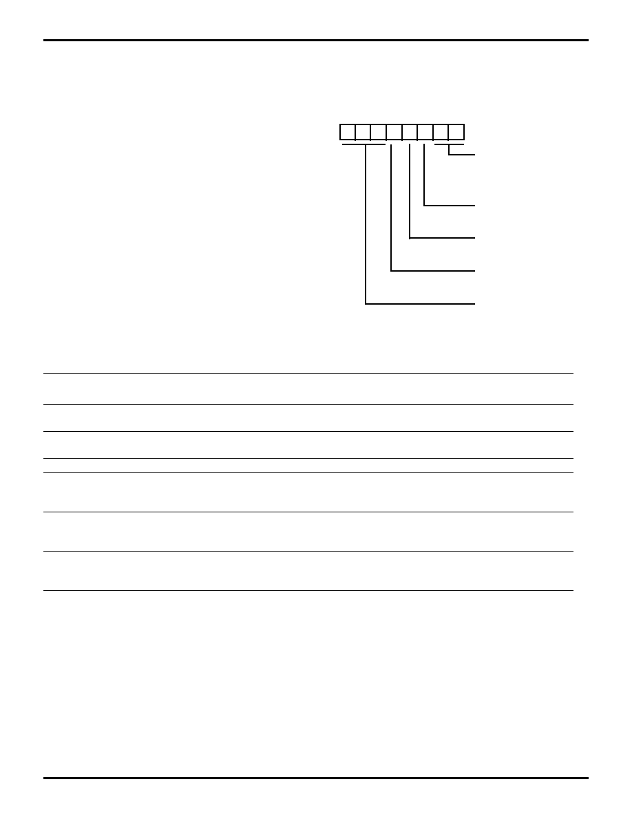
Expanded Register File. The register file has been ex-
panded to allow for additional system control registers and
for mapping of additional peripheral devices and input/out-
put ports into the register address area. The Z8 register
address space R0 through R15 is implemented as 16
groups of 16 registers per group. These register groups
are known as the ERF (Expanded Register File). Bits 3-0
of the Register Pointer (RP) select the active ERF group.
Bits 7-4 of register RP select the working register group
(Figure 11). Three system configuration registers reside in
the Expanded Register File address space in Bank F,
while six PN modulator registers reside in Bank C. The rest
of the Expanded Register addressing space is not physi-
cally implemented and is open for future expansion. To
write to the ERF, the upper nibble of the RP must be zero.
To write to the rest of the register file, the lower nibble must
be zero.
Antiheroine using Zilog's cross assembler Version 2.1 or
earlier, use theLD RP, #0X instruction rather than the SRP
#0X instruction to access the ERF.
Figure 10. Program Memory Map
12
11
10
9
8
7
6
5
4
3
2
1
0
On-Chip
ROM
Location of
First Byte of
Instruction
Executed
After RESET
Interrupt
Vector
(Lower Byte)
Interrupt
Vector
(Upper Byte)
IRQ5
IRQ4
IRQ4
IRQ3
IRQ3
IRQ2
IRQ2
IRQ1
IRQ1
IRQ0
IRQ0
IRQ5
1023
Z87100
Zilog
Wireless Transmitter
DS96WRL0700
P R E L I M I N A R Y
3-15
3
Figure 11. Expanded Register File Architecture
7
6
5
4
3
2
1
0
Working Register
Group Pointer
Expanded Register
Group Pointer
%FF
%FO
%7F
%0F
%00
Z8 Reg. File
REGISTER POINTER
% FF
% FE
% FD
% FC
% FB
% FA
% F9
% F8
% F7
% F6
% F5
% F4
% F3
% F2
% F1
% F0
SPL
GPR
RP
FLAGS
IMR
IRQ
IPR
P01M
P3M
P2M
PRE0
T0
PRE1
T1
TMR
U
U
0
U
0
0
U
U
U
1
U
U
U
U
0
U
U
0
U
U
0
U
U
U
1
U
U
U
U
0
U
U
0
U
U
0
U
U
U
1
U
U
U
U
0
U
U
0
U
U
0
U
0
U
1
U
U
U
U
0
U
U
0
U
U
0
U
U
U
1
U
U
U
U
0
U
U
0
U
U
0
U
U
U
1
U
U
U
U
0
U
U
0
U
U
0
U
U
0
1
U
U
0
U
0
U
U
0
U
U
0
U
U
0
1
0
U
0
U
0
1
1
U
U
U
U
U
U
U
U
U
U
U
U
U
U
U
U
U
REGISTER
EXPANDED REG. GROUP (F)
RESET CONDITION
REGISTER
REG. GROUP (0)
RESET CONDITION
REGISTER
Z8 STANDARD CONTROL REGISTERS
RESET CONDITION
% (0) 03
P3
% (0) 02
P2
% (0) 01
Reserved
% (0) 00
Reserved
Not Implemented
D7 D6 D5 D4 D3 D2 D1 D0
*
*
*
*
Reserved
EXPANDED REG. GROUP (C)
U
U
U
U
U
U
U
U
% (F) 0F
% (F) 0E
% (F) 0D
% (F) 0C
% (F) 0B
% (F) 03
% (F) 02
% (F) 01
% (F) 00
WDTMR
SMR
Reserved
Reserved
Reserved
Reserved
Reserved
Reserved
PCON
% (F) 0A
Reserved
% (F) 09
Reserved
% (F) 08
Reserved
% (F) 07
Reserved
% (F) 06
Reserved
% (F) 05
Reserved
% (F) 04
Reserved
U
U
U
0
1
1
0
1
1*
U
U
U
U
0
0
0
1
0
0
0
0
0
1*
1*
U = Unknown
= Reserved
Legend:
Will not be reset with a
STOP-Mode Recovery
*
Resets upon power-on according
to RC/TMBASE mask option.
**
% (C) 04
TxBUFH
% (C) 03
TxBUFL
% (C) 02
PNLEN
% (C) 01
PNADDR
% (C) 06
TMBAS
% (C) 05
DCLK
% (C) 00
PNCON
REGISTER
RESET CONDITION
U
U
U
0
**
0
0
0
U
U
U
U
U
U
U
U
U
U
U
U
U
U
U
U
0
0
0
0
0
0
0
0
U
U
U
U
U
U
U
U
U
U
U
U
U
U
U
U
0
0
0
0
0
0
0
0
*
*
*
*
*
*
*
U
Z87100
Wireless Transmitter
Zilog
3-16
P R E L I M I N A R Y
DS96WRL0700
FUNCTIONAL DESCRIPTION (Continued)
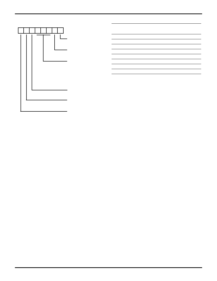
Register File. The Register File consists of two I/O port
registers, 124 general-purpose registers, 15 control and
status registers, and ten system configuration registers in
the Expanded Register Group, including six registers in
support of the PN modulator. The instructions can access
registers directly or indirectly through an 8-bit address
field, allowing use of a short 4-bit register address with the
Register Pointer. In the 4-bit mode, the Register File is di-
vided into 16 working register groups, each occupying 16
continuous locations. The Register Pointer addresses the
starting location of the active working-register group.
Caution: D4 of Control Register P01M (R248) must be
0. If the Z87100 is emulated by Z86C90, D4 of P01M
has to change to 0 before submission to ROM code.
GPR. The Z87100 has one extra general-purpose register
located at %FE(R254).
Figure 12. Register Pointer
D7 D6 D5
D4 D3
D2 D1 D0
Expanded Register File Pointer
Working Register Pointer
R253 RP
Figure 13. Register Pointer
The upper nibble of the register file address
provided by the register pointer specifies
the active working-register group.
r7
r6
r5
r4
R253 (%FD)
(Register Pointer)
I/O Ports
Specified Working
Register Group
The lower nibble
of the register
file address
provided by the
instruction points
to the specified
register.
r3
r2
r1
r0
Register Group 1
Register Group 0
R31 to R16
Register Group F
R15 to R4
R3 to R0
R127 to R111
∑
∑
∑
∑
∑
7F
70
0F
00
1F
10
2F
20
∑
∑
∑
∑
∑
∑
∑
∑
∑

Z87100
Zilog
Wireless Transmitter
DS96WRL0700
P R E L I M I N A R Y
3-17
3
Stack. The Z87100 has an 8-bit Stack Pointer (R255) used
for the internal stack that resides within the 124 general-
purpose registers.
Counter/Timers. There are two 8-bit programmable
counter/timers (T0-T1), each driven by its own 6-bit pro-
grammable prescaler. The T1 prescaler can be driven by
internal or external clock sources, however, the T0 pres-
caler is driven by the internal clock only (Figure 14).
Figure 14. Counter/Timer Block Diagram
PRE0
Initial Value
Register
T0
Initial Value
Register
T0
Current Value
Register
6-Bit
Down
Counter
8-Bit
Down
Counter
˜
16
˜
4
6-Bit
Down
Counter
8-Bit
Down
Counter
PRE1
Initial Value
Register
T1
Initial Value
Register
T1
Current Value
Register
Clock
Logic
IRQ4
TOUT
P36
IRQ5
Internal Data Bus
Write
Write
Read
Internal Clock
Gated Clock
Triggered Clock
TIN
P31
Write
Write
Read
Internal Data Bus
External Clock
Internal
Clock
(SCLK)
(SMR) D0
˜
4
˜
2
˜
2
OSC
0
0
(SMR) D1
1
1
Z87100
Wireless Transmitter
Zilog
3-18
P R E L I M I N A R Y
DS96WRL0700
FUNCTIONAL DESCRIPTION (Continued)
The 6-bit Prescaler divide the input frequency of the clock
source by any integer number from 1 to 64. Each prescaler
drives its counter, which decrements the value (1 to 256)
that has been loaded into the counter. When the counter
reaches the end of count, a timer interrupt request, IRQ4
(T0) or IRQ5 (T1), is generated.
The counters are programmed to start, stop, restart to con-
tinue, or restart from the initial value. The counters can
also be programmed to stop upon reaching zero (single-
pass mode) or to automatically reload the initial value and
continue counting (modulo-n continuous mode).
The counters, but not the Prescaler, may be read at any
time without disturbing their value or count mode. The
clock source for T1 is user-definable and can be either the
internal microprocessor clock divided by four, or an exter-
nal signal input through Port 3. The Timer Mode register
configures the external timer input (P31) as an external
clock, a trigger input that can be retriggerable or non-retrig-
gerable, or as a gate input for the internal clock. Port 3, line
P36 serves as a timer output (T
OUT
) through which T0, T1
or the internal clock can be output. The counter/timers can
be cascaded by connecting the T0 output to the input of
T1.
Interrupts. The Z87100 has six different interrupts from
six different sources. The interrupts are maskable and pri-
oritized (Figure 15). The six sources are divided as follows;
two sources are claimed by Port 3 lines P31 and P33, two
sources in the counter/timers, one source for the PN mod-
ulator and one source for the time base generator. The In-
terrupt Mask Register globally or singularly enables or dis-
ables the six interrupt requests (Table 2).
Figure 15. Interrupt Block Diagram
Interrupt
Edge
Select
IRQ (D6, D7)
IRQ1, 3, 4, 5
IRQ
IMR
IPR
PRIORITY
LOGIC
6
Global
Interrupt
Enable
Vector Select
Interrupt
Request
IRQ0 IRQ2

Z87100
Zilog
Wireless Transmitter
DS96WRL0700
P R E L I M I N A R Y
3-19
3
When more than one interrupt is pending, priorities are re-
solved by a programmable priority encoder that is con-
trolled by the Interrupt Priority register. An interrupt ma-
chine cycle is activated when an interrupt request is
granted. This disables all subsequent interrupts, saves the
Program Counter and Status Flags, and then branches to
the program memory vector location reserved for that in-
terrupt. All Z87100 interrupts are vectored through loca-
tions in the program memory. This memory location and
the next byte contain the 16-bit starting address of the in-
terrupt service routine for that particular interrupt request.
To accommodate polled interrupt systems, interrupt inputs
are masked and the interrupt request register is polled to
determine which of the interrupt requests needs services.
When the PN modulator is disabled, IRQ3 has no hard-
ware source but can be invoked by software by setting bit
D3 of the IRQ register to 1. When the PN modulator is en-
abled, an interrupt will be mapped to IRQ3 after the con-
tents of the PN modulator's data hold register have been
loaded into the modulator's data shift register.
An interrupt resulting from AN1 (P31) is mapped into IRQ2,
and an interrupt from the time base generator is mapped
into IRQ0. Interrupts IRQ2 and IRQ0 may be rising, falling,
or both-edge triggered, and are programmable by the us-
er. The software can poll to identify the state of the pin. For
IRQ0 and the time base generator, selection of the trigger
edge is not critical but should not be changed once select-
ed.
The programming bits for the INTERRUPT EDGE SE-
LECT are located in the IRQ register (R250), bits D7 and
D6. The configuration is shown in Table 3.
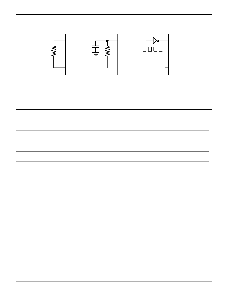
Clock. The Z87100 derives its timing from an on-board RC
oscillator referenced as RC or an external clock source ap-
plied to the time base counter input referenced as TM-
BASE. The RC clock source is made of an internal oscilla-
tor and an external resistor and an optional external
capacitor (See Figure 14).
The 2 terminals that are part of the RC oscillator are refer-
enced as RC1 and RC2. The frequency of the clock signal
generated by the RC oscillator cannot exceed 6 MHz. RC1
can also be driven by an external clock source, while RC2
remains unconnected. In this configuration the Z87100
can be clocked up to 12 MHz, when not in Low EMI mode.
(4 MHz in Low EMI mode).
Both clock sources, RC and TMBASE, can be selected to
drive the internal Z8 system clock, depending on the set-
ting of a mask-programmed option bit.
The TMBASE clock input requires a 32.768 kHz clock sig-
nal when the TMBASE is enabled or when the TMBASE is
selected to be the default oscillator. As a special feature of
the Z87100, ICC current consumption is significantly re-
duced at a clock frequency of 10 kHz in low EMI noise
mode.
Table 2. Interrupt Types, Sources, and Vectors
Name
Source
Vector
Location
Comments
IRQ0
Time Base
0, 1
Internal,
Rising/Falling Edge
Triggered
IRQ1
IRQ1
2, 3
External (P33),
Falling Edge
Triggered
IRQ2
IRQ2, TIN
4, 5
External (P31),
Rising/Falling Edge
Triggered
IRQ3
Software/PN
Modulator
6, 7
Software
Generated/Internal*
IRQ4
T0
8, 9
Internal
IRQ5
TI
10, 11
Internal
Notes:
*When the PN Modulator is enabled, IRQ3 is an internal
interrupt.
Table 3. IRQ0 and IRQ2 Interrupt Edge
Programming
IRQ
Register D7
IRQ
Register D6
P31
Interrupt
Edge Time
Base
0
0
F
F
0
1
F
R
1
0
R
F
1
1
R/F
R/F
Notes:
F = Falling Edge
R = Rising Edge
Z87100
Wireless Transmitter
Zilog
3-20
P R E L I M I N A R Y
DS96WRL0700
FUNCTIONAL DESCRIPTION (Continued)
Recovery Timer Circuit. A timer circuit clocked by a ded-
icated on-board WDT oscillator or by the RC oscillator or
TMBASE clock oscillator is used as a recovery timer. The
timer allows V
CC
and the oscillator circuit to stabilize be-
fore instruction execution begins. The recovery timer cir-
cuit is a one-shot timer triggered by one of the three con-
ditions:
s
Power Fail to Power OK status
s
Stop-Mode Recovery (If D5 of SMR=1)
s
WDT Time-Out
The recovery time is a nominal 5 ms using the internal
WDT oscillator or, if used with the WDT, 256 clock cycles
of the selected externally referenced oscillator. Bit 5 of the
Stop Mode Register determines whether the recovery tim-
er is bypassed after Stop-Mode Recovery.
HALT. The HALT instruction turns off the internal CPU
clock but not the selected RC oscillator or TMBASE clock.
The counter/timers and external interrupts IRQ0 and IRQ2
remain active. The device is recovered by interrupts, either
externally or internally generated. After the interrupt, exe-
cution proceeds to the next instruction following the HALT
instruction.
STOP. This instruction turns off the internal clock and the
RC oscillation and reduces the standby current to 10
µ
A or
less. The STOP mode is terminated by either WDT time-
out, POR, or SMR recovery. Either of these events causes
the processor to restart the application program at address
000C (HEX). Note that the selected clock source, RC os-
cillator or TMBASE clock, remains active if bits 3 and 4 of
the WDTMR are set. In this mode, only the watch-dog tim-
er runs and the time base generator always remain on.
Figure 16. RC Oscillator Configuration
RC1
RC2
External Clock
RC Oscillator
C
RC1
RC2
R
RC1
RC2
R
Table 4. Maximum Clock Value in Different Modes
Standard Mode
SCLK=RC1/2
Standard Mode
SCLK=RC1
Low EMI
SCLK= RC1/2
Low EMI
SCLK=RC1
Ext Clock
12 MHz
(SCLK=6 MHz)
6 MHz
(SCLK = 6 MHz)
4 MHz
(SCLK = 2 MHz)
2 MHz
(SCLK = 2 MHz)
RC
6 MHz
(SCLK = 3 MHz)
3 MHz
(SCLK = 3 MHz)
1 MHz
(SCLK = 500 kHz)
500 kHz
(SCLK = 500 kHz)

Z87100
Zilog
Wireless Transmitter
DS96WRL0700
P R E L I M I N A R Y
3-21
3
In order to enter STOP (or HALT) mode, it is necessary to
first flush the instruction pipeline to avoid suspending exe-
cution in mid-instruction. To do this, the user executes a
NOP (opcode=FFH) immediately before the appropriate
sleep instruction; i.e.,
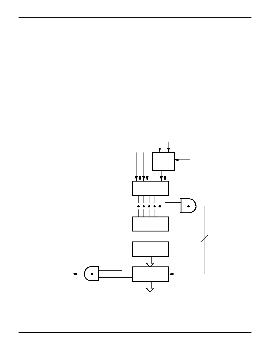
PN Modulator. The Z87100 incorporates a PN modulator
to allow generation of a direct sequence spread spectrum
data stream. Coupled with the appropriate transmitter cir-
cuitry, the Z87100 can support wireless and power line
spread spectrum transmission.
The PN modulator of the Z87100 is shown in Figure 15.
Major elements of the PN modulator include the PN ROM,
the PN modulator control logic, the data hold and data
shift registers, and the clock select multiplexor and PN and
data clock generator.
As part of the PN modulator, a specially designated area
of ROM (PN ROM) provides space for 256 bits ("chips") of
one or more pseudorandom noise sequences. The PN
modulator control logic accesses the PN ROM as a circular
buffer and synchronously exclusive-or's (XORs) each chip
of the sequence with the data bits loaded in the PN modu-
lator's data shift register, thereby PN modulating the data.
The PN code is accessed from the PN ROM beginning at
a specified relative address (PNADDR, register %02 in
bank C of the Expanded Register Group) until the chip cor-
responding to the PN code length (PNLEN, register %03 in
bank C of the Expanded Register Group) is reached, at
which point access continues again from the specified rel-
ative address.
The limits of the PN ROM address space are automatically
resolved by the control logic so that the PN ROM is effec-
tively a large circular buffer from which smaller circular
buffers defined by PNLEN and PNADDR can be access-
ed. Operation and control of the circular buffer is transpar-
ent to the user. As long as the sum of code lengths is less
than or equal to 256 chips, more than one PN sequence
may be ROM programmed, with the choice of code or even
a concatenation of codes to be used for transmission con-
trolled by Z8 software and the values of PNADDR and PN-
LEN.
Contents of PN ROM are shifted out and XOR'ed with the
contents of the data shift register. The rates at which the
two streams are shifted are controlled by the PN and data
clocks so that one or more PN chips are XOR'ed against a
single data bit, where the number of PN chips is deter-
mined by the value of PNLEN. The reference clock for the
PN modulator may be selected from the internal system
clock (SCLK) or either of the two counter/timers (T0 and
T1).
In nominal operation, the PN clock is defined by the select-
ed reference clock, and the data clock is then generated as
an integer fraction of the PN clock, where the integer is
specified by PNLEN. In this way, each data bit can be syn-
chronously modulated by a full PN code sequence as de-
fined by PNLEN, PNADDR, and the contents of PN ROM.
As a practical matter, this type of symbol-synchronous PN
modulation allows the corresponding spread spectrum re-
ceiver to be designed with improved acquisition perfor-
mance -- since the PN and data modulation are synchro-
nously related at the transmitter, PN acquisition at the
receiver can simultaneously establish bit synchronization.
FF
NOP; clear the pipeline
6F
STOP; enter STOP mode
or
FF
NOP; clear the pipeline
7F
HALT; enter HALT mode

Z87100
Wireless Transmitter
Zilog
3-22
P R E L I M I N A R Y
DS96WRL0700
FUNCTIONAL DESCRIPTION (Continued)
While nominal operation assumes that a single PN se-
quence of PNLEN chips corresponds to a single data bit as
described above, the PN modulator additionally supports
modes which allow 2 or 4 bits per PN sequence or 2 or 4
PN sequences per bit or an arbitrary relationship between
the PN and data clocks. The specific relationship between
the selected reference clock, the PN clock, and the data
clock then depends upon the values of the PNLEN and
DCLK registers.
The Z8 loads the data shift register of the PN modulator by
writing to the PN modulator's 16-bit data hold register, Tx-
BUFL and TxBUFH. As the last bit of the data shift register
is shifted to be XOR'ed, the PN modulator's control logic
loads the contents of the data hold register into the data
shift register and triggers interrupt IRQ3. Loading of the
next byte of data to TxBUFL and TxBUFH can thus be con-
trolled by Z8 software through interrupts or through polling
by using IRQ3.
Initiation of PN modulation is controlled by three control
bits in the PNCON and TMBASE control registers:
PN_ENABLE,PN_MODULATE,and
MODULATE_SELECT.
PN _ENABLE (PNCON D0) enables the PN modulator by
providing its circuitry with clock signals and configures
IRQ3 and P35 of Port 3.
PN_MODULATE (PNCON D6) initializes the PN ROM ad-
dress counter to the start of the PN sequence, loads the
data shift register with the contents of the data hold regis-
ter, TxBUFH and TxBUFL, and, depending on the value of
MODULATE_SELECT, either begins PN modulation of the
data or begins transmission of the unmodulated PN se-
quence.
MODULATE_SELECT (TMBASE D4) controls whether
the contents of the data hold register are clocked out to be
PN modulated. If MODULATE_SELECT is set to 0, the
contents of PN ROM and the data hold register will then be
clocked out to be XOR'ed together; otherwise, if
MODULATE_SELECT is set to 1, only the contents of PN
ROM will be clocked out.
Typically, one would enable the PN modulator with
PN_ENABLE, select the desired PN code sequence from
PN ROM using PNLEN and PNADDR, configure the de-
sired PN and data clocks using REF_CLOCK_SELECT,
DATA_CLOCK_MODE and DCLK, and select the desired
outputs using PNCLKOUT_ENABLE, PNDOUT_ENABLE
and PNDCLKOUT_ENABLE. With the first data to be
transmitted loaded in the data hold register TxBUFL and
TXBUFH, transmission of PN modulated data or just the
PN code sequence can then begin under control of
PN_MODULATE and MODULATE_SELECT.
PN Modulator I/O. The Z87100 PN modulator outputs and
inputs are multiplexed with the pins of Ports 2 and 3 ac-
cording to Table 4. By enabling the PN modulator with
PN_ENABLE (D0 of PN Modulator Control Register 1,
PNCON1), the PN-modulated data output, PNMODOUT,
is automatically multiplexed to P35. Selection of the other
PN modulator outputs, however, requires explicit enabling
of the associated control bits in PNCON as well as
PN_ENABLE. In that way, as few as one or as many as
four I/O pins may be used in operation of the PN modula-
tor, depending upon the application's requirements.

Z87100
Zilog
Wireless Transmitter
DS96WRL0700
P R E L I M I N A R Y
3-23
3
Figure 17. Z87100 PN Modulator Conceptual Block Diagram
PN ROM
256 x 1
CLOCK
GENERATOR
XOR
PN MODULATOR
CONTROL
LOGIC
CLOCK
SELECT
SCLK
T0
T1
clk select
clk ctrl
DATA HOLD REGISTER
DATA SHIFT REGISTER
D0
D1
D14 D15
PNCLKOUT
(P36)
PNMODOUT
(P35)
PNDCLKOUT
(P27)
PNDOUT
(P20)
dataclk
data load
CPU
DATA
BUS
IRQ3
ROM
Address
Counter
8
pnclk
pnload
PNLEN
PNADDR
8
8
refclk
pnclk
Tx BUFL Tx BUFH
PNLEN
PNADDR
PNCON
DCLK
TMBAS
SHIFT CTL

Z87100
Wireless Transmitter
Zilog
3-24
P R E L I M I N A R Y
DS96WRL0700
FUNCTIONAL DESCRIPTION (Continued)
PN Modulator Registers
The PN modulator is supported by six read/write registers
located in bank (C) of the Expanded Register Group: the
PN modulator control register (PNCON) at %(C)00; the PN
relative address register (PNADDR) at %(C)01; the PN
code length register (PNLEN) at %(C)02; the PN modula-
tor low-byte data hold register (TxBUFL) at %(C)03; the
high-byte data hold register (TxBUFH) at %(C)04; and the
data clock control register (DCLK) at %(C)05. Internally,
the PN modulator also contains the data shift register for
the chips and data bits to be XOR'ed.
PNCON
The PN control register, PNCON, shown in Figure 18 and
located at %(C)00, controls the operation and configura-
tion of the Z87100's PN modulator. PNCON provides the
following control functions:
PN_ENABLE (PNCON D0) disables or enables the PN
modulator. When disabled (PN_ENABLE=0), clock signals
to the PN modulator circuitry are discontinued, reducing
the overall Z87100 power requirements. When enabled
(PN_ENABLE=1), the PN-spread output PNMODOUT is
automatically directed to P35 of Port 3 and the pins indicat-
ed in Table 4 may, under program control, be selected as
indicated.
Enabling the PN modulator further configures interrupt
IRQ3 to monitor the status of the PN modulator's data shift
register. IRQ3 will initially be cleared (set to 0) but will be
set to 1 after the last bit of the data shift register's contents
has been PN-modulated and the current contents of Tx-
BUFL and TxBUFH have been automatically transferred to
the data shift register. The user then has at most 16 data
bit intervals in which to update TxBUFL and TxBUFH.
IRQ3 may be used to control data input to the PN modula-
tor either as an interrupt or as a polled flag, depending on
whether the EI instruction has been invoked. As an inter-
rupt, IRQ3 will be automatically cleared as the interrupt is
serviced; as a polled flag, IRQ3 must be cleared each time
by manually setting bit 3 of the register to 0.
REF_CLOCK_SELECT (PNCON D1:D2) selects which of
three sources (SCLK, T0, or T1) is used as the PN clock.
PNCLKOUT_ENABLE (PNCON D3) when enabled
(D3=1), selects P36 of Port 3 as the output pin for the PN
modulator's PN clock. PN_ENABLE must be set.
PNDOUT_ENABLE (PNCON D4), when enabled (D5=1),
selects P20 of Port 2 as the output pin for the unspread
data stream. PN_ENABLE must be set, and P20 must be
configured as an output pin using P20OE of the P2M Port
2 Mode Register.
PNDCLKOUT_ENABLE (PNCON D5), when enabled
(D6=1), selects P27 of Port 2 as the output pin for the un-
spread data's clock. PN_ENABLE must be set, and P27
must be configured as an output pin using P27OE of the
P2M Port 2 Mode Register.
PN_MODULATE (PNCON D6) turns the PN modulation
function on and off, starting and stopping its operation
once enabled by PN_ENABLE. Setting PN_MODULATE
to 1 from 0 loads the data shift register with the current
contents of the data hold register, TxBUFL and TxBUFH,
and initializes the PN ROM address counter to the start of
the PN sequence according to the value set in PNADDR.
If MODULATE_SELECT is set to 0, the contents of PN
ROM and the data hold register will then be clocked out to
be XOR'ed together; otherwise, if MODULATE_SELECT
is set to 1, only the contents of PN ROM will be clocked
out.
Table 5. PN Modulator Registers
Pin Name
Location
I/O
Function
PNDOUT
P20
output
unspread data
output
PNDCLKOUT
P27
output data
clock
output
PNMODOUT
P35
output
PN spread data
output
PNCLKOUT
P36
output
PN clock output
Figure 18. PN Modulator Control Register (PNCON)
D7
D6
D5
D4
D3
D2
D1
D0
PN_ENABLE
0 Disable
1 Enable
REF_CLOCK_SELECT
00 SCLK
01 T0
1X T1
PNCLKOUT_ENABLE
0 P36 I/O
1 P36 PNCLKOUT
PNDOUT_ENABLE
0 P20 I/O
1 P20 DCLKOUT
PNDCLKOUT_ENABLE
0 P27 I/O
1 P27 PNDCLKOUT
PN_MODULATE
0 STOP
1 START
DATA_CLOCK MODE
0 PNLEN-Dependent Data Clock
1 Independent Data Clock

Z87100
Zilog
Wireless Transmitter
DS96WRL0700
P R E L I M I N A R Y
3-25
3
Resetting PN_MODULATE to 0 from 1 stops PN modula-
tion after the current data byte is completely modulated;
i.e., after either the high or low byte of the current contents
of the 16-bit data shift register is completely modulated.
The timing of the command to reset PN_MODULATE must
be monitored by the user, based on the number of cycles
after IRQ3 was last raised, in order to insure that the de-
sired byte is the last byte transmitted.
When instructed to stop, the contents of TxBUFL and Tx-
BUFH will not be transferred to the data shift register. Set-
ting PN_MODULATE to 1 will then completely reinitiate PN
modulation beginning with the PN sequence starting at
PNADDR (i.e., the PN sequence will be reset) and with the
data word to be modulated as currently stored in the PN
modulator's data hold register, TxBUFL and TxBUFH. In
effect, the data shift register contents are flushed when PN
modulation is stopped.
DATA_CLOCK_MODE (PNCON D7) controls whether the
data and PN clocks are integrally related. When
DATA_CLOCK_MODE equals 0, the data and PN clocks
are integrally related as determined by bits D0, D1, and D2
of register DCLK and the value of PNLEN. When
DATA_CLOCK_MODE equals 1, the PN clock is deter-
mined by the selected reference clock and PNLEN while
the data clock is independently determined by the refer-
ence clock and DCLK.
PNADDR
The PN relative address register, PNADDR at %(C)01, in-
dicates the starting address within PN ROM to access the
PN sequence to be used in modulation. Addressing is rel-
ative, with PNADDR=00H corresponding to the first PN
chip contained in PN ROM, PNADDR=FFH corresponding
to the last. The value of PNADDR must be set prior to start-
ing operation of the PN modulator; writing to PNADDR
while PN modulation is in process will give indeterminate
results.
PNLEN
The PN code length register, PNLEN at %(C)02, indicates
the number of PN chips to be accessed from PN ROM and
modulated against each data bit. If the value of PNLEN
plus PNADDR exceeds FFH, the PN modulator's control
logic will automatically cycle through PN ROM so that a to-
tal of PNLEN chips are utilized. In some modes, the value
of PNLEN also determines the data rate, where the PN
modulator's data shift register is clocked by an integer mul-
tiple or fraction of the selected reference clock divided by
PNLEN. The value of PNLEN must be set prior to starting
operation of the PN modulator; writing to PNLEN while PN
modulation is in process will give indeterminate results.
TxBUFL and TxBUFH
The PN modulator's data hold register, TxBUFL at %(C)03
and TxBUFH at %(C)04, supports the loading of data bytes
by the Z8 core for PN modulation. Data loading may be
controlled either through software polling or interrupt using
IRQ3. The time available to load data depends upon the
transmit data rate, itself a function of the speed of the se-
lected reference clock and the value of PNLEN, and, of
course, upon the Z87100 clock.
Note that the data shift register is clocked by the dataclk.
Data is shifted for PN modulation D15 first, D0 last in terms
of the data loaded into TxBUFL and TxBUFH. The data
shift register, as opposed to TxBUFL and TxBUFH, is not
accessible by the CPU.
DCLK
The data clock control register, DCLK at %(C)05, deter-
mines the relationship within the PN modulator among the
PN clock controlling the PN shift register (pnclk), the data
clock controlling the data shift register (dataclk), and the
selected reference clock (SCLK, or one of the two Z8
counter/timers). A conceptual drawing of the PN modula-
tor's timing generator is shown in Figure 17, while Table 5
summarizes the following discussion of the various data
clock modes.
When DATA_CLOCK_MODE (PNCON D7) is set to 0, the
first three bits of DCLK (D2, D1, D0) establish an integral
relationship between the data clock and the PN code se-
quence.

Z87100
Wireless Transmitter
Zilog
3-26
P R E L I M I N A R Y
DS96WRL0700
FUNCTIONAL DESCRIPTION (Continued)
Nominal operation corresponds to DCLK D2=0, D1=0, and
D0=0: the PN clock (pnclk) is then equal to the reference
clock (refclk), and the data clock is equal to refclk divided
by the value of PNLEN. In this way, a complete PN code
sequence as defined by PNLEN corresponds to a single
data bit. The PN modulator output is thus the PN sequence
with its polarity determined by the value of the data bit.
With D2=0, non-zero values of D1 and D0 determine if ref-
clk/PNLEN is further divided by 2D1 D0 to form the data
clock. In other words,
pnclk = refclk,
dataclk = pnclk/(PNLEN x 2D1 D0),
As can be seen, a single data bit may correspond to 2, 4,or
8 PN sequences in this mode.
With D2=1, the PN clock is formed by dividing refclk by 4.
The values of D1 and D0 then determine the relationship
of dataclk to refclk and can allow a single PN sequence to
correspond to 2 or 4 data bits:
pnclk = refclk/4,
dataclk = refclk/(PNLEN x 2D1 D0)
or, equivalently,
dataclk = (4/2D1 D0) x pnclk/PNLEN.
When DATA_CLOCK_MODE (PNCON D7) is set to 1, the
number of complete PN code sequences per data bit or
number of data bits per single PN code sequence is not
necessarily an integer. The PN clock is defined by refclk,
while the data clock is determined as refclk/DCLK, using
all 8 bits of DCLK. Although not likely to be used, DCLK =
00H corresponds to a value of 256. The transition edges of
a single chip are still aligned with that of a bit transition, but
the PN code cycle is not necessarily synchronous with
data transitions.
Figure 19. Conceptual Block Diagram of PN Modulator Timing Generator
Clock
Select
refclk
pnclk
(to PN ROM)
DCLK D2
PNCON D7
(DATA_CLOCK_MODE)
˜
4
1
0
˜
PNLEN
˜
2
D1 D0
dataclk
(to DATA SHIFT
REGISTER)
0
˜
DCLK
1
DCLK
D1 D0
PNCON
DATA_CLOCK_MODE
SCLK
T0
T1
D7
0 dataclk
integrally related
to pnclk
1 independent
dataclk

Z87100
Zilog
Wireless Transmitter
DS96WRL0700
P R E L I M I N A R Y
3-27
3
Time Base Generator. The time base generator can be
used while the Z8 is in stop mode to initiate a stop-mode
recovery or while the Z8 is operating to generate IRQ0 in-
terrupts as a time-keeping pulse. If used while the Z8 is in
stop mode, time-out will trigger a stop-mode recovery
("warm start") and reset the processor to address 000C
(hex). Otherwise, time-out of the time base generator will
set IRQ0 to 1. This mode can be used while the Z8 contin-
ues operation and a regular time base is desired, where
IRQ0 can either be polled as a flag and manually cleared
by the user or enabled as an interrupt and automatically
cleared. The time base generator is programmable and
can provide clock signals every .25 seconds, one second,
one minute, or one hour, with control of the time base gen-
erator provided through the TMBASE register at %(C)06.
TMBASE
The time base generator control register, located at
%(C)06 and depicted in Figure 18, allows the time base to
be selected and its actions controlled.
TIMEOUT_SELECT. (TMBASE D0-D1) determines the
time base. A value of D1=0, D0=0 selects .25 seconds; 01
selects one second; 10 selects one minute; and 11 selects
one hour.
If the external time base clock input is not connected to an
external clock source, pin 10 should be connected to
ground.
TIMEOUT_ENABLE. (TMBASE D2) enables and disables
the time base generator. When set to 0,
TIMEOUT_ENABLE stops current operation of the time
base generator. When set to 1, TIMEOUT_ENABLE re-
sets and starts the time base generator. Reading
TIMEOUT_ENABLE provides an indication of the time
base generator's status: if set to 0, the time base generator
is off; if set to 1, the generator is currently operating.
CLOCK_SELECT. (TMBASE D3) selects either RC or
TMBASE as the clock for the Z8. If set to 0, RC will be the
clock for the Z87100; if set to 1, TMBASE will be the clock.
Determination of which clock is used upon Power-On Re-
set ("cold start") is mask-programmable, to be selected by
the customer at the time ROM code is submitted. Upon a
Stop-Mode Recovery warm start, however, the value of
this bit (as is true for all the values of this register) is not
reset. As a result, a customer could, for example, mask-
program the Z87100 to power-up using RC and then, un-
der software control, switch. Depending on the application,
operation during the wake cycle could then be conducted
using either RC or TMBASE.
Table 6. Data and PN Clock Configuration
DATA_CLOCKMODE
DCLK
PNCLK
DATACLK
0
xxxxx000
refclk
pnclk/PNLEN
0
xxxxx001
refclk
pnclk/(PNLENx2)
0
xxxxx010
refclk
pnclk/(PNLENx4)
0
xxxxx011
refclk
pnclk/(PNLENx8)
0
xxxxx100
refclk/4
4xpnclk/PNLEN
0
xxxxx101
refclk/4
2xpnclk/PNLEN
0
xxxxx110
refclk/4
pnclk/PNLEN
0
xxxxx111
refclk/4
pnclk/(PNLENx2)
1
DCLK
refclk
pnclk/DCLK
Z87100
Wireless Transmitter
Zilog
3-28
P R E L I M I N A R Y
DS96WRL0700
FUNCTIONAL DESCRIPTION (Continued)
The time base generator, if mask-optioned, are always on,
but RC is off when not selected. When switching from TM-
BASE to RC, internal circuitry waits for 128 valid clock cy-
cles of TMBASE (4 msec @ 32 kHz) before effecting the
switch from TMBASE to RC to insure that RC has stabi-
lized. Internal circuitry also insures that the switch from RC
to TMBASE or TMBASE to RC is glitch-free. It is recom-
mended that any command to switch oscillators be fol-
lowed by a loop that tests the value of CLOCK_SELECT:
the value of CLOCK_SELECT will only change when the
transition has fully taken place.
MODULATE_SELECT. (TMBASE D4) controls the clock-
ing out of data from the PN modulator's data shift register.
If MODULATE_SELECT is set to 0, the contents of PN
ROM and the data hold register will be clocked out to be
XOR'ed together; otherwise, if MODULATE_SELECT is
set to 1, only the contents of PN ROM will be clocked out.
Timing of this operation depends on whether the data and
PN clocks are integrally related, as determined by
DATA_CLOCK_MODE, and whether PN modulation has
begun, as determined by PN_MODULATE, as shown in
Table 7.
Figure 20. Time Base Generator Control Register
D7
D6
D5
D4
D3
D2
D1
D0
TIMEOUT_SELECT
0 0 0.25 Second
0 1 1.0 Second
1 0 1 Minute
1 1 1 Hour
CLOCK_SELECT
Reserved
TIMEOUT_ENABLE
0 Disabled (stop)
1 Enabled (reset and start)
0 RC
1 TMBASE
MODULATE_SELECT
0 PN-modulated data
1 PN sequence only
Table 7. PN Modulation Stop/Start Control
PN_MODULATE
0
1
MODULATE_SELECT=0
(PN-Modulated Data)
First data bit and first PN chip of the PN code sequence will be clocked out
together at the next edge of the data clock (dclk).
MODULATE_SELECT=1
(PN Sequence Only)
First PN chip of the PN chip sequence will be clocked out at the next edge
of the data clock (dclk).
PN_MODULATE=1
MODULATE_SELECT 1
0
(PN Only
PN + Data)
If DATA_CLOCK_MODE=0 (integer number of PN code sequences per
bit), then the first data bit will be clocked out with the next repetition of the
first PN chip of the PN code sequence.
If DATA_CLOCK_MODE=1 (independent PN code sequence length and
data bit duration). then the first data bit will be clocked out at the the next
edge of the data clock (dclk) together with the ongoing PN sequence.
MODULATE_SELECT 0
1
(PN + Data
PN Only)
Last data bit will be clocked out with the immediately preceding edge of the
data clock (dclk); code sequence output will continue according to the PN
clock (pnclk).
Z87100
Zilog
Wireless Transmitter
DS96WRL0700
P R E L I M I N A R Y
3-29
3
Stop-Mode Recovery Register (SMR). This register se-
lects the clock divide value and determines the mode of
Stop-Mode Recovery (Figure 19). All bits are write only ex-
cept bit 7, which is read only. Bit 7 is a flag bit that is hard-
ware set on the condition of a STOP recovery and reset on
a power-on cycle. Bit 6 controls whether a low level or high
level is required from the recovery source. Bit 5 controls
the reset delay after recovery. Bits 2, 3, and 4 of the SMR
specify the source of the Stop-Mode Recovery signal. Bit
1 determines whether the selected oscillator, RC or TM-
BASE, is divided by 1 or 2. Bit 0 controls the divide-by-16
prescaler of SCLK/TCLK.
SCLK/TCLK divide-by-16 select (D0). D0 of the SMR
controls a divide-by-16 prescaler of SCLK/TCLK. The pur-
pose of this control is to selectively reduce device power
consumption during normal processor execution (SCLK
control) and/or HALT mode (where TCLK sources the
counter/timers and interrupt logic).
RC1 Clock divide-by-two (D1). This bit determines
whether the RC1 clock is divided by two or one. When this
bit is set to 1, the SCLK/TCLK is equal to the RC1 clock.
This option can work together with the low EMI options in
PCON register to reduce the EMI noise. Maximum clock
frequency is 6 MHz when divide-by-one selection is active.
Stop-Mode Recovery Source (D2,D3,D4). These three
bits of the SMR specify the wake-up source of the Stop-
Mode Recovery (Figure 21 and Table 8).
P31 and P33 cannot wake up from STOP mode if the input
lines are configured as analog inputs.
Stop-Mode Recovery Delay Select (D5). This bit dis-
ables the nominal 5 ms RESET delay provided by the re-
covery timer circuit after Stop-Mode Recovery. The default
condition of this bit is 1, enabling the delay. If this bit is 0,
the extra delay is disabled, limiting the recovery delay to 18
cycles of RC1.
Stop-Mode Recovery Level Select (D6). A 1 in this bit
position indicates that a high level on any one of the recov-
ery sources wakes the device from STOP mode. A 0 indi-
cates low level recovery. The default is 0 on POR (Figure
19).
Cold or Warm Start (D7). This bit is READ only. When the
device enters STOP mode, D7 will be set to 1. D7 will only
be reset to 0 to indicate "cold" start if the device is reset by
either a Power-On Reset or by a Watch-Dog Timer Reset
when the part is in normal operation. Otherwise, if the de-
vice is reset by a Watch-Dog Timer Reset when the part is
in STOP mode or by any other SMR source, then this bit
will continue to be set to 1 to indicate a "warm" start.
Reset Upon Power-On. Upon applying power to the
Z87100, an internal reset pulse is generated which triggers
the timing recovery circuit illustrated in Figure 22. Power-
on reset (POR) behavior is different, however, depending
on whether RC or TMBASE has been selected as the clock
that drives the Z8
Æ
.
When RC is mask-selected to be the Z8 system clock, the
recovery counter is clocked by an internal WDT (Watch-
Dog Timer) oscillator. The system reset initiated by POR
takes 5 ms and guarantees that the RC oscillations are
stabilized before the first instruction is executed by the Z8.
Subsequently, the recovery counter is used as the Watch-
Dog Timer.
When TMBASE is mask-selected to be the default Z8 sys-
tem clock upon power-on, recovery timing is controlled by
the time base generator.
Figure 21. Stop-Mode Register
D7 D6
D5
D4
D3
D2
D1
D0
SMR (F) 0B
SCLK/TCLK Divide by 16
0 OFF
1 ON
Stop-Mode Recovery Source
000 POR Only
001 POR Only
010 P31
011 Time Base Generator
100 P33
101 P27
110 P2 NOR 0:3
111 P2 NOR 0:7
Stop Delay
0 OFF
1 ON
Stop Recovery Level
0 Low Level
1 High Level
Stop Flag
0 POR
1 Stop Recovery
*
Default setting after RESET
*
*
*
*
*
Clock Divide
0 SCLK = RC1/2*
1 SCLK = RC1
Table 8. Stop-Mode Recovery Source
SMR
D4
SMR
D3
SMR
D2
Operation
Description of Action
0
0
0
POR recovery only
0
0
1
POR recovery only
0
1
0
P31 transition
0
1
1
Time Base Generator
1
0
0
P33 transition
1
0
1
P27 transition
1
1
0
Logical NOR of Port 2 bits 0-3
1
1
1
Logical NOR of Port 2 bits 0-7
Z87100
Wireless Transmitter
Zilog
3-30
P R E L I M I N A R Y
DS96WRL0700
FUNCTIONAL DESCRIPTION (Continued)
Watch-Dog Timer Mode Register (WDTMR). The WDT
is a retriggerable one-shot timer that resets the Z8 if it
reaches its terminal count. The WDT is initially enabled by
executing the WDT instruction and retriggered on subse-
quent executions of the WDT instruction. The WDT timer
circuit is driven by an on-board WDT oscillator or external
clock source RC. The WDT does not use TMBASE. The
WDT timer clock source is selected with bit 4 of the WDT-
MR to use either the internal WDT oscillator and a reset
delay of 5 ms, or RC1 and a reset delay of 512 RC1 clock
cycles. Note that the WDT instruction may affect the zero,
sign, and overflow flags.
Bits 0 and 1 control a tap circuit that determines the WDT
time-out period. Bit 2 determines whether the WDT is ac-
tive during HALT and bit 3 determines WDT activity during
STOP. If bits 3 and 4 of this register are both set to 1, only
the WDT is only driven by the external clock during STOP
mode. This feature makes it possible to wake up from
STOP mode from an internal source. Bits 5 through 7 of
the WDTMR are reserved (Figure 23).
The WDTMR register is accessible only during the first 64
processor cycles (128 oscillator clocks) from the execution
of the first instruction after Power-On-Reset, Watch Dog
Reset or a Stop-Mode Recovery (Figure 22). After this
point, the register cannot be modified by any means, inten-
tional or otherwise. The WDTMR cannot be read and is lo-
cated in bank F of the Expanded Register Group at ad-
dress location 0FH, as shown in Figure 23.
Note: The POR, with TMBASE the default Z8 clock
source, takes 1.5 seconds the first instruction is exe-
cuted by the Z8.
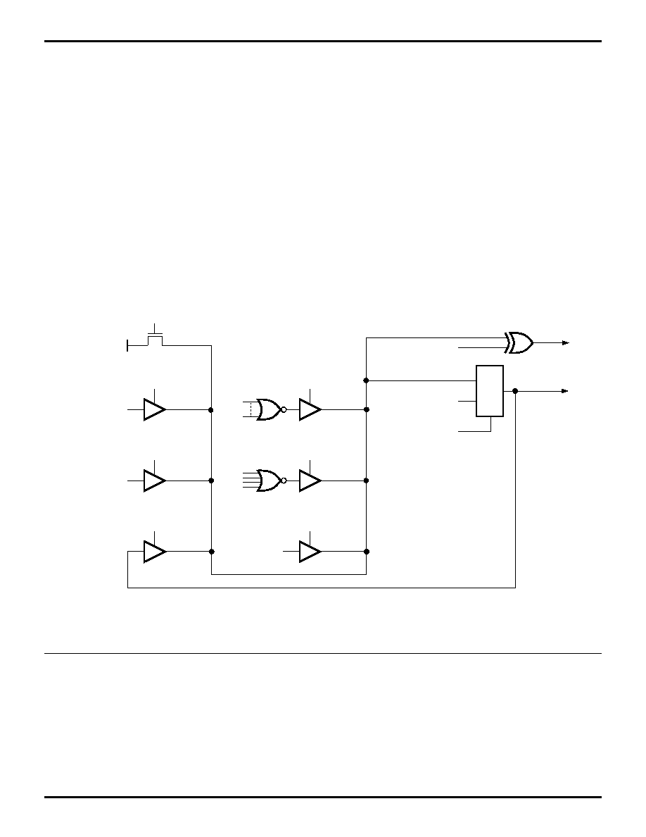
Figure 22. Stop-Mode Recovery Source
VDD
P31
P33
SMR D4
0
D3
1
D2
0
SMR D4
1
D3
0
D2
0
SMR D4
0
0
D3
0
0
D2
0
1
XTALB
Time Base
Generator
SMR D4
0
D3
1
D2
1
SMR D4
1
D3
1
D2
1
P20
P27
SMR D4
1
D3
1
D2
0
P20
P23
P27
SMR D4
1
D3
0
D2
1
Stop Mode Recovery
Edge Select (SMR)
MUX
P33 From Pads
Digital/Analog Mode
Select (P3M)
To P33 Data
Latch and IRQ1
To POR
Reset

Z87100
Zilog
Wireless Transmitter
DS96WRL0700
P R E L I M I N A R Y
3-31
3
WDT Time Select (D1,D0). Selects the WDT time-out pe-
riod. It is configured as shown in Table 9.
WDT During HALT (D2). This bit determines whether or
not the WDT is active during HALT mode. A 1 indicates ac-
tive during HALT. The default is 1.
WDT During STOP (D3). This bitdetermines whether or
not the WDT is active during STOP mode. A 1 indicates
active during STOP. The default is 1. If bits D3 and D4 are
both set to 1, then only the WDT is driven by the external
clock during STOP mode.
On-Board WDT Oscillator or RC Oscillator Select (D4).
This bit determines which oscillator source is used to clock
the internal recovery and WDT counter chain. If the bit is a
1, the internal WDT oscillator is bypassed and the recovery
and WDT clock source is driven from RC1. The default
configuration of this bit is 0, which selects the internal WDT
oscillator.
V
CC
Voltage Comparator. An on-board Voltage Compar-
ator checks that V
CC
is at the required level to ensure cor-
rect operation of the device. Reset is globally driven if V
CC
is below the specified voltage (typically 2.1V).
Low-Voltage Protection (V
LV
). The low voltage trip volt-
age (V
LV
) will be less than 3 volts and above 1.4 volts un-
der the following conditions.
Maximum (V
LV
) Conditions:
T
A
= 0
∞
, +70
∞
C, Internal Clock Frequency
equal or less than 2 MHz
Notes: The internal clock frequency is one half the
external clock frequency, unless the device is divide-by-
one mode.
The device functions normally at or above 3.0V under all
conditions. Below 3.0V, the device functions normally until
the Low-Voltage Protection trip point (V
LV
) is reached, for
the temperatures and operating frequencies described
above. The device is guaranteed to function normally at
supply voltages above the low voltage trip point. The actu-
al low voltage trip point is a function of temperature and
process parameters (Figure 23).
ROM Protect. ROM protect is mask-programmable. It is
selected by the customer at the time the ROM code is sub-
mitted. The selection of ROM protect disables the LDC and
LDCI instructions.
Table 9. WDT Time Select
D1
D0
Time-out of
internal WDT
OSC
Time-out of
RC7 clock
0
0
5 ms min
512TpC
0
1
15 ms min
1024TpC
1
0
25 ms min
2048TpC
1
1
100 ms min
8192TpC
Note: The default on a WDT initiated RESET is 15 ms.
Figure 23. Watch-Dog Timer Mode Register
D7
D6
D5
D4
D3
D2
D1
D0
WDTMR (F) 0F
WDT TAP INT WDT OSC RC7 CLK
00 5 512 TpC
01 15 1024 TpC*
10 25 2048 TpC
11 100 8192 TpC
WDT During HALT
0 OFF
1 ON
WDT During STOP
0 OFF
1 ON
RC/WDT OSC Select for WDT
0 WDT Oscillator
1 RC7 Oscillator
Reserved (Must be 0)
*
Default setting after RESET
*
*
*
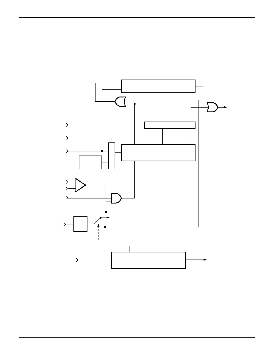
Z87100
Wireless Transmitter
Zilog
3-32
P R E L I M I N A R Y
DS96WRL0700
FUNCTIONAL DESCRIPTION (Continued)
Z87100 Mask Options. The following summarizes the
mask options to be selected by the customer at the time of
ROM code submittal:
RC/TMBASE
Determine whether "cold start" Initialization: uses RC or
TMBASE as base clock.
ROM Protect
Selects ROM protect.
On/Off:
Figure 24. Timing Recovery Circuit (POR, WDT)
CLK
18 Clock RESET
Generator
RESET
Clear
WDT TAP SELECT
WDT
OSC
CLK
CLR
5 ms Recovery 5 ms 15 ms 25 ms 100 ms
Internal
RESET
WDT Select
(WDTMR) D1-D0
CLK Select
(WDTMR) D4
RC7
VCC
2V REF
+
-
WDT/Recovery Counter Chain
M
U
X
WDT
From
Stop Mode
Recovery Source
1
0
12 ns
Glitch
Filter
Stop Delay Select (SMR D5)
TMBASE
Time Base Counter
(.25s, 1s, 1 min, 1 hr)
Power-On Recovery

Z87100
Zilog
Wireless Transmitter
DS96WRL0700
P R E L I M I N A R Y
3-33
3
EXPANDED REGISTER FILE CONTROL REGISTERS
Figure 25. Typical Z87100 V
LV
Voltage vs Temperature
VCC
(Volts)
2.60
2.20
2.00
1.80
1.60
1.40
-60
-40
-20
0
20
40
60
80
100
120
140
2.80
2.40
Temperature (
∞
C)
V (Typical)
LV
Figure 26. Stop-Mode Recovery Register
((F) 0BH: Write Only)
D7
D6
D5
D4
D3
D2
D1
D0
SMR (F) 0B
SCLK/TCLK Divide by 16
0 OFF *
1 ON
Stop-Mode Recovery Source
000 POR Only
001 POR Only
010 P31
011 Time Base
100 P33
101 P27
110 P2 NOR 0:3
111 P2 NOR 0:7
Stop Delay
0 OFF
1 ON *
Stop Recovery Level
0 Low Level *
1 High Level
Stop Flag (Read Only)
0 POR *
1 Stop Recovery
*
Default setting after RESET
*
Clock Divide
0 RC/2
1 RC
Note: Register settings are not reset upon Stop-Mode Recovery.
Figure 27. Watch-Dog Timer Mode Register
((F) 0FH: Write Only)
D7
D6
D5
D4
D3
D2
D1
D0
WDTMR (F) 0F
WDT TAP WDT OSC RC CLK
00 5 512 TpC
01 15 1024 TpC *
10 25 2048 TpC
11 100 8192 TpC
WDT During HALT
0 OFF
1 ON*
WDT During STOP
0 OFF
1 ON*
RC/WDT OSC Select for WDT
0 WDT Oscillator
*
1 RC Oscillator
Reserved (Must be 0)
*
Default setting after RESET
Note: Register settings are not reset upon Stop-Mode Recovery.

Z87100
Wireless Transmitter
Zilog
3-34
P R E L I M I N A R Y
DS96WRL0700
EXPANDED REGISTER FILE CONTROL REGISTERS (Continued)
Figure 28. PORT Control Register
((F) 00H: Write Only)
Figure 29. Reserved
Figure 30. Timer Mode Register
(F1H: Read/Write)
D7 D6
D5
D4
D3
D2
D1
D0
Comparator
Output PORT 3
0 P34, P35 Standard Output
*
1 P34, P35 Comparator Output
Low EMI Noise
PORT 3
0 Low EMI Noise
1 Standard
*
Low EMI Noise
PORT 2
0 Low EMI Noise
1 Standard
*
Reserved (Must be 1)
PCON (F) 00
Low EMI RC Oscillator
0 Low EMI Noise
1 Standard
*
*
Default Setting After Reset.
D7 D6 D5 D4 D3 D2 D1 D0
Reserved (Must be 0)
R 240
D7
D6
D5
D4
D3
D2
D1
D0
0 Disable T0 Count
1 Enable T0 Count
0 No Function
1 Load T0
0 No Function
1 Load T1
0 Disable T1 Count
1 Enable T1 Count
TIN Modes
00 External Clock Input
01 Gate Input
10 Trigger Input
(Non-retriggerable)
11 Trigger Input
(Retriggerable)
TOUT Mode
00 Not Used
01 T0 OUT
10 T1 OUT
11 Internal Clock Out (P36)
R241 TMR
Figure 31. Counter Timer 1 Register
(F2H: Read/Write)
Figure 32. Prescaler 1 Register
(F3H: Write Only)
Figure 33. Counter/Timer 0 Register
(F4H: Read/Write)
D7 D6
D5
D4
D3
D2
D1
D0
T0 Initial Value
(When Written)
(Range: 1-256 Decimal
01-00 HEX)
T0 Current Value
(When READ)
R244 T0
D7
D6
D5
D4
D3
D2
D1
D0
Count Mode
0 T1 Single Pass
1 T1 Modulo-N
Clock Source
1 T1 Internal
0 T1 External Timing Input
(TIN ) Mode
Prescaler Modulo
(Range: 1-64 Decimal
01-00 HEX)
R243 PRE1
D7
D6
D5
D4
D3
D2
D1
D0
T0 Initial Value
(When Written)
(Range: 1-256
Decimal
01-00 HEX)
T0 Current Value
(When READ)
R244 T0

Z87100
Zilog
Wireless Transmitter
DS96WRL0700
P R E L I M I N A R Y
3-35
3
Figure 34. Prescaler 0 Register
(F5H: Write Only)
Figure 35. PN Modulator Control Register
((C) 00H: Read/Write)
Figure 36. PN ROM Relative Address Register
((C) 01H: Read/Write)
D7
D6
D5
D4
D3
D2
D1
D0
Count Mode
0 T0 Single Pass
1 T0 Modulo N
X
Prescaler Modulo
(Range: 1-64 Decimal
01-00 HEX)
R245 PRE0
D7
D6
D5
D4
D3
D2
D1
D0
PN_ENABLE
0 Disable
1 Enable
REF_CLOCK_SELECT
00 SCLK
01 T0
1X T1
PNCLKOUT_ENABLE
0 P36 I/O
1 P36 PNCLKOUT
PNDOUT_ENABLE
0 P20 I/O
1 P20 DCLKOUT
PNDCLKOUT_ENABLE
0 P27 I/O
1 P27 PNDCLKOUT
PNCON (C) 00
PN_MODULATE
0 STOP
1 START
DATA_CLOCK_MODE
0 PNLEN-dependent data clock
1 Independent data clock
Note: Register settings are not reset upon Stop-Mode Recovery.
D7 D6 D5 D4 D3 D2 D1 D0
PNADDR (C) 01
PNADDR = PN sequence
starting address
Note: Register settings are not reset upon Stop-Mode Recovery.
Figure 37. PN Code Length Register
((C) 02H: Read/Write)
Figure 38. PN Modulator Low-Byte
Data Hold Register ((C) 03H: Write Only)
Figure 39. PN Modulator High-Byte
Data Hold Register ((C) 04H: Write Only)
Figure 40. Data Clock Control Register
((C) 05H: Read/Write)
D7
D6
D5
D4
D3
D2
D1
D0
PNLEN (C) 02
PNLEN = PN sequence length
Note: Register settings are not reset upon Stop-Mode Recovery.
D7
D6
D5
D4
D3
D2
D1
D0
TxBUFH (C) 04
TxBUFH = X
Note: Register settings are not reset upon Stop-Mode Recovery.
D7
D6
D5
D4
D3
D2
D1
D0
TxBUFH (C) 04
TxBUFH = X
Note: Register settings are not reset upon Stop-Mode Recovery.
D7
D6
D5
D4
D3
D2
D1
D0
DCLK (C) 05
When DATA_CLOCK_MODE
(PNCON D7) = 0,
dataclk = refclk/2D1-D0
D2 = 0: pnclk = refclk
D2 = 1: pnclk = refclk/4
When DATA_CLOCK_MODE
(PNCON D7) = 1,
pnclk = refclk
dataclk = refclk/DCLK
Note: Register settings are not reset upon Stop-Mode Recovery.
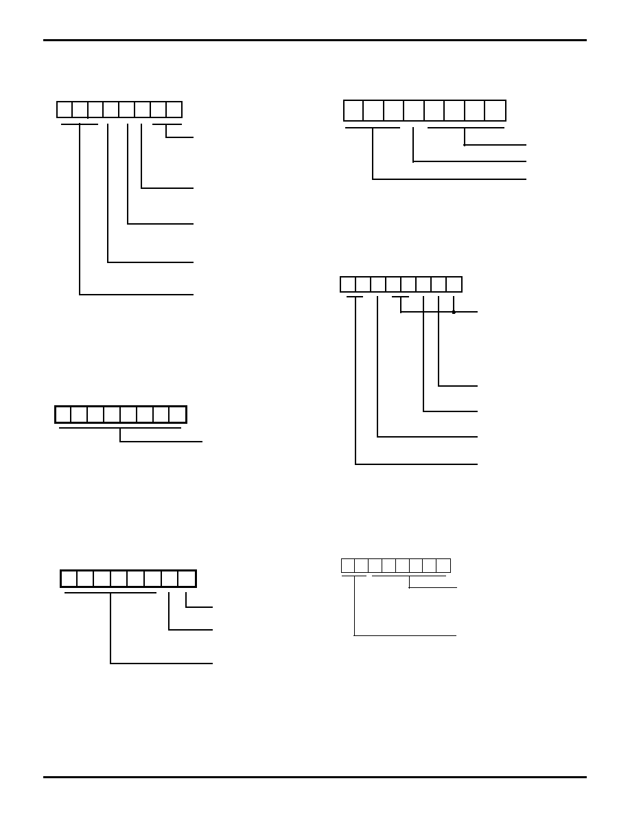
Z87100
Wireless Transmitter
Zilog
3-36
P R E L I M I N A R Y
DS96WRL0700
EXPANDED REGISTER FILE CONTROL REGISTERS (Continued)
Figure 41. Time Base Generator
Control Register ((C) 06H: Read/Write)
Figure 42. Port 2 Mode Register
(F6H; Write Only)
Figure 43. Port 3 Mode Register
(F7H: Write Only)
D7
D6
D5
D4
D3
D2
D1
D0
TIMEOUT_SELECT
TMBAS (C) 06
0 0 0.25 second
0 1 1.0 second
1 0 1 minute
1 1 1 hour
TIMEOUT_ENABLE
0 Disabled (stop)
1 Enabled (reset and start)
CLOCK_SELECT
0 RC
1 TMBASE
Reserved
Note: Register settings are not reset upon Stop-Mode Recovery.
MODULATE_SELECT
0 PN modulated data
1 PN sequence only
D7
D6
D5
D4
D3
D2
D1
D0
P2 - P2 I/O Definition
0 Defines Bit as OUTPUT
1 Defines Bit as INPUT
7
0
R246 P2M
Note: Register settings are not reset upon Stop-Mode Recovery.
D7
D6
D5
D4
D3
D2
D1
D0
0 Port 2 Open-Drain
1 Port 2 Push-Pull
Port 3 Inputs
0 Digital
1 Analog
0 Reserved
R247 P3M
Note: Register settings are not reset upon Stop-Mode Recovery.
Figure 44. Port 0 and 1 Mode Register
(F8H: Write Only)
Figure 45. Interrupt Priority Register
(F9H: Write Only)
Figure 46. Interrupt Request Register
(FAH: Read/Write)
D7
D6
D5
D4
D3
D2
D1
D0
X
Must be 0
X
R248 P01M
D7
D6
D5
D4
D3
D2
D1
D0
Interrupt Group Priority
000 Reserved
001 C > A > B
010 A > B > C
011 A > C > B
100 B > C > A
101 C > B > A
110 B > A > C
111 Reserved
IRQ3, IRQ5 Priority (Group A)
0 IRQ5 > IRQ3
1 IRQ3 > IRQ5
IRQ0, IRQ2 Priority (Group B)
0 IRQ2 > IRQ0
1 IRQ0 > IRQ2
IRQ1, IRQ4 Priority (Group C)
0 IRQ1 > IRQ4
1 IRQ4 > IRQ1
0
R249 IPR
D7
D6
D5
D4
D3
D2
D1
D0
IRQ0 = XTALB Time Base Generator
IRQ1 = P33 Input
IRQ2 = P31 Input
IRQ3 = Software Controlled/PN Modulator
IRQ4 = T0
IRQ5 = T1
Interrupt On Edge
00 P31
XTALB Time Base
01 P31
XTALB Time Base
10 P31
XTALB Time Base
11 P31
XTALB Time Base
R250 IRQ

Z87100
Zilog
Wireless Transmitter
DS96WRL0700
P R E L I M I N A R Y
3-37
3
Figure 47. Interrupt Mask Register
(FBH: Read/Write)
Figure 48. Flag Register
(FCH: Read/Write)
D7
D6
D5
D4
D3
D2
D1
D0
0 Reserved
1 Enables IRQ5-IRQ0
(D0= IRQ0)
1 Enables Interrupts
R251 IMR
D7
D6
D5
D4
D3
D2
D1
D0
User Flag F1
User Flag F2
Half Carry Flag
Decimal Adjust Flag
Overflow Flag
Sign Flag
Zero Flag
Carry Flag
R252 Flags
Figure 49. Register Pointer
(FDH: Read/Write)
Figure 50. General-Purpose Register
(FEH: Read/Write)
Figure 51. Stack Pointer
(FFH: Read/Write)
D7 D6
D5
D4 D3
D2
D1
D0
Expanded Register File Pointer
Working Register Pointer
R253 RP
D7
D6
D5
D4
D3
D2
D1
D0
R254 GPR
D7
D6
D5
D4
D3
D2
D1
D0
Stack Pointer Lower
Byte (SP0- SP7 )
R255 SPL

Z87100
Wireless Transmitter
Zilog
3-38
P R E L I M I N A R Y
DS96WRL0700
DEVICE CHARACTERISTICS
Figure 52. Typical I
CC
vs Frequency
Current
(mA)
12
8
6
4
2
0
0
2
4
6
8
10
12
14
16
10
Frequency (MHz)
Icc at 5V
Icc at 3.3V
Icc1 at 5V
Icc1 at 5V
(SCLK divided by 16)
Icc1 at 3.3V
Icc1 at 3.3V
(SCLK divided by 16)
Note:RC is divided by 2
Figure 53. Typical V
OL
, V
IL
vs Temperature
1.0
2.0
-20
0
40
60
80
B
Vcc
(Volts)
A = VIL at Vcc = 3.3V
B = VIL at Vcc = 5.5V
C = VOL at Vcc = 3.0V
D = VOL at Vcc = 5.5V
Temperature (
∞
C)
100
-40
20
140
Legend:
-60
120
A
C
D
0.0
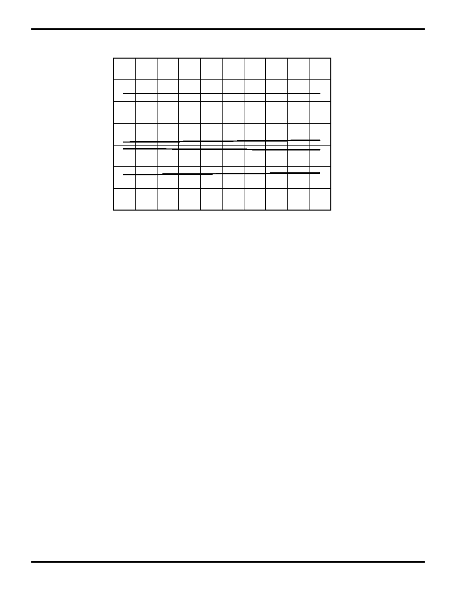
Z87100
Zilog
Wireless Transmitter
DS96WRL0700
P R E L I M I N A R Y
3-39
3
Figure 54. Typical V
OH
, V
IH
vs Temperature
Vcc
(Volts)
6.0
4.0
3.0
2.0
1.0
0
-60
-40
-20
0
20
40
60
80
100
120
140
8.0
5.0
Temperature (
∞
C)
VOH at Vcc 5.5V
VIH at Vcc = 5.5V
VOH at Vcc 3.0V
VIH at Vcc = 3.0V
Note: STD Mode
(Not Low EMI Mode)
Z87100
Wireless Transmitter
Zilog
3-40
P R E L I M I N A R Y
DS96WRL0700
DEVICE CHARACTERISTICS (Continued)
Figure 55. Typical V
OH
vs I
OH
Over Temperature
IOH
(mA)
-1.0
-3.0
-4.0
-5.0
-6.0
-7.0
1.0
2.0
3.0
4.0
5.0
6.0
0
-2.0
V (Volts)
-8.0
-9.0
7.0
8.0
0
Vcc = 3.0V
Vcc = 5.0V
Vcc = 5.5V
A
B
C
D E F G H I
Legend:
A = 125
∞
C
B = 25
∞
C
C = -55
∞
C
D = 125
∞
C
E = 25
∞
C
F = -55
∞
C
G = 125
∞
C
H = 25
∞
C
I = -55
∞
C
OH
Note: STD Mode
(Not Low EMI Mode)

Z87100
Zilog
Wireless Transmitter
DS96WRL0700
P R E L I M I N A R Y
3-41
3
Figure 56. Typical I
OL
vs V
OL
Over Temperature
0
2.0
4.0
6.0
8.0
10.0
12.0
14.0
16.0
18.0
20.0
22.0
24.0
0
0.2
0.4
0.6
0.8
1.0
1.2
1.4
1.6
1.8
IOL
(mA)
V (Volts)
A
B
C D
E
F
Legend:
A = -55
∞
C
B = 25
∞
C
C = 125
∞
C
D = -55
∞
C
E = 25
∞
C
F = 125
∞
C
Vcc = 5.5V
Vcc = 3.0V
OL
Note: STD Mode
(Not Low EMI Mode)

Z87100
Wireless Transmitter
Zilog
3-42
P R E L I M I N A R Y
DS96WRL0700
DEVICE CHARACTERISTICS (Continued)
Figure 57. Typical Power-On Reset Time vs Temperature
0
2.0
4.0
6.0
8.0
10.0
12.0
14.0
16.0
18.0
20.0
-60
-40
-20
0
20
40
60
80
100
120
Time
(ms)
Temperature (
∞
C)
140
Legend:
A - Vcc = 3.0V
B - Vcc = 3.5V
C - Vcc = 4.0V
D - Vcc = 4.5V
E - Vcc = 5.0V
F - Vcc = 5.5V
A
B
C
D
E
F
22.0
Note: Using WDT Oscillator
Z87100
Zilog
Wireless Transmitter
DS96WRL0700
P R E L I M I N A R Y
3-43
3
Figure 58. Typical 5 ms WDT Setting vs Temperature
0
5.0
10.0
15.0
20.0
25.0
30.0
35.0
40.0
-60
-40
-20
0
20
40
60
80
100
120
Time
(ms)
Temperature (
∞
C)
140
Legend:
A - Vcc = 3.0V
B - Vcc = 3.5V
C - Vcc = 4.0V
D - Vcc = 4.5V
E - Vcc = 5.0V
F - Vcc = 5.5V
45.0
A
B
C
D
E
F
Note: Using WDT Oscillator

Z87100
Wireless Transmitter
Zilog
3-44
P R E L I M I N A R Y
DS96WRL0700
DEVICE CHARACTERISTICS (Continued)
Figure 59. Typical 15 ms WDT Setting vs Temperature
-60
-40
-20
0
20
40
60
80
100
120
Time
(ms)
Temperature (
∞
C)
140
Legend:
A - Vcc = 3.0V
B - Vcc = 3.5V
C - Vcc = 4.0V
D - Vcc = 4.5v
E - Vcc = 5.0V
F - Vcc = 5.5V
85
80
75
70
65
60
55
50
45
40
35
30
25
20
15
10
5
0
A
B
C
D
E
F
Note: Using WDT Oscillator

Z87100
Zilog
Wireless Transmitter
DS96WRL0700
P R E L I M I N A R Y
3-45
3
Figure 60. Typical 25 ms WDT Setting vs Temperature
-60
-40
-20
0
20
40
60
80
100
120
Time
(ms)
Temperature (
∞
C)
140
Legend:
A - Vcc = 3.0V
B - Vcc = 3.5V
C - Vcc = 4.0V
D - Vcc = 4.5v
E - Vcc = 5.0V
F - Vcc = 5.5V
170
160
150
140
130
120
110
90
80
70
60
50
40
30
20
10
0
A
B
C
D
E
F
Note: Using WDT Oscillator
Z87100
Wireless Transmitter
Zilog
3-46
P R E L I M I N A R Y
DS96WRL0700
DEVICE CHARACTERISTICS (Continued)
Figure 61. Typical 100 ms WDT Setting vs Temperature
-60
-40
-20
0
20
40
60
80
100
120
Time
(ms)
Temperature (
∞
C)
140
Legend:
A - Vcc = 3.0V
B - Vcc = 3.5V
C - Vcc = 4.0V
D - Vcc = 4.5v
E - Vcc = 5.0V
F - Vcc = 5.5V
700
650
600
550
500
450
400
350
300
250
200
150
100
50
0
A
B
C
D
E
F
Note: Using WDT Oscillator

Z87100
Zilog
Wireless Transmitter
DS96WRL0700
P R E L I M I N A R Y
3-47
3
Figure 62. Typical Frequency vs RC Resistance
0
0
Frequency
(MHz)
Resistance (Kohms)
40
Legend:
A - VCC = 5.0V
±
10%; no external capacitor
B - VCC = 5.0V
±
10%; external capacitor = 22 pF
10
A
B
