
ZiLOG Worldwide Headquarters ∑ 910 E. Hamilton Avenue ∑ Campbell, CA 95008
Telephone: 408.558.8500 ∑ Fax: 408.558.8300 ∑
www.ZiLOG.com
Z87200
Spread-Spectrum
Transceiver
Product Specification
PS010202-0601

Z87200
Spread-Spectrum Transceiver
PS010202-0601
This publication is subject to replacement by a later edition. To determine whether
a later edition exists, or to request copies of publications, contact:
ZiLOG Worldwide Headquarters
910 E. Hamilton Avenue
Campbell, CA 95008
Telephone: 408.558.8500
Fax: 408.558.8300
www.ZiLOG.com
ZiLOG is a registered trademark of ZiLOG Inc. in the United States and in other countries. All other
products and/or service names mentioned herein may be trademarks of the companies with which
they are associated.
Document Disclaimer
©2001 by ZiLOG, Inc. All rights reserved. Information in this publication concerning the devices,
applications, or technology described is intended to suggest possible uses and may be superseded.
ZiLOG, INC. DOES NOT ASSUME LIABILITY FOR OR PROVIDE A REPRESENTATION OF
ACCURACY OF THE INFORMATION, DEVICES, OR TECHNOLOGY DESCRIBED IN THIS
DOCUMENT. ZiLOG ALSO DOES NOT ASSUME LIABILITY FOR INTELLECTUAL PROPERTY
INFRINGEMENT RELATED IN ANY MANNER TO USE OF INFORMATION, DEVICES, OR
TECHNOLOGY DESCRIBED HEREIN OR OTHERWISE. Devices sold by ZiLOG, Inc. are covered
by warranty and limitation of liability provisions appearing in the ZiLOG, Inc. Terms and Conditions of
Sale. ZiLOG, Inc. makes no warranty of merchantability or fitness for any purpose. Except with the
express written approval of ZiLOG, use of information, devices, or technology as critical components
of life support systems is not authorized. No licenses are conveyed, implicitly or otherwise, by this
document under any intellectual property rights.

4-1
4
P
RODUCT
S
PECIFICATION
Z87200
4
S
PREAD
-S
PECTRUM
T
RANSCEIVER
FEATURES
s
Complete Direct Sequence Spread-Spectrum
Transceiver in a Single CMOS IC
s
Programmable Functionality Supports Many Different
Operational Modes
s
Acquires Within One Symbol Duration Using Digital PN
Matched Filter
s
Two Independent PN Sequences, Each up to 64 Chips
Long for Distinct Processing of the Acquisition/Preamble
Symbol and Subsequent Data Symbols
s
Power Management Features
s
Optional Spectral Whitening Code Generation
s
Full- or Half-Duplex Operation
Benefits
s
High Performance and High Reliability for Reduced
Manufacturing Costs
s
Ideal for a Wide Range of Wireless Applications
Including Data Acquisition Systems, Transaction
Systems, and Wireless Local Area Networks (WLANs)
s
Fast Response and Very Low Overhead when
Operating in Burst Modes
s
Allows High Processing Gain to Maximize the
Acquisition Probability, then Reduced Code Length for
Increased Data Rate
s
Reduced Power Consumption
s
Randomizes Data to Meet Regulatory Requirements
s
Permits Dual Frequency (Frequency Division Duplex) or
Single Frequency (Time Division Duplex) Operation
s
Small Footprint, Surface Mount
GENERAL DESCRIPTION
The Z87200 is a programmable single-chip, spread-spec-
trum, direct-sequence transceiver. The Z87200 incorpo-
rates Stanford Telecom spread-spectrum and wireless
technology and is identical to Stanford Telecom's STEL-
2000A. By virtue of its fast acquisition capabilities and its
ability to support a wide range of data rates and spread-
spectrum parameters, the Z87200 spread-spectrum trans-
ceiver supports the implementation of a wide range of
burst data communications applications.
Available in both 45- and 20-MHz versions, the Z87200
performs all the digital processing required to implement a
fast-acquisition direct sequence (such as pseudonoise- or
PN-modulated), spread-spectrum full- or half-duplex sys-
tem. Differentially encoded BPSK and QPSK are fully sup-
ported. The receiver section can also handle differentially
encoded pi/4 QPSK. A block diagram of the Z87200 is
shown in Figure 1; its pin configuration is shown in Z87200
receive functions integrate the capabilities of a digital
downconverter, PN matched filter, and DPSK demodula-
tor, where the input signal is an analog-to-digital converted
I.F. signal. Z87200 transmit functions include a differential
BPSK/QPSK encoder, PN modulator (spreader), and
BPSK/QPSK modulator, where the transmitter output is a
sampled digitally modulated signal ready for external digi-
Device
Min
PN Rate*
(Mchips)
Max Data
Rate* (Mbps)
Speed
(MHz)
Package
Z87200
11
2.048
20/45
100-Pin
PQFP
Note:
*45 MHz only
PS010202-0601

Z87200
Spread-Spectrum Transceiver
Zilog
4-2
GENERAL DESCRIPTION
(Continued)
tal-to-analog conversion (or, if preferred, the spread base-
band signal may be output to an external modulator).
These transceiver functions have been designed and inte-
grated for the transmission and reception of bursts of
spread data. In particular, the PN Matched Filter has two
distinct PN coefficient registers (rather than a single one)
in order to speed and improve signal acquisition perfor-
mance by automatically switching from one to the other
upon signal acquisition. The Z87200 is thus optimized to
provide reliable, high-speed wireless data communica-
tions.
Symbol-Synchronous PN Modulation
The Z87200 operates with symbol-synchronous PN mod-
ulation in both transmit and receive modes. Symbol-syn-
chronous PN modulation refers to operation where the PN
code is aligned with the symbol transitions and repeats
once per symbol. By synchronizing a full PN code cycle
over a symbol duration, acquisition of the PN code at the
receiver simultaneously provides symbol synchronization,
thereby significantly improving overall acquisition time.
As a result of the Z87200's symbol-synchronous PN mod-
ulation, the data rate is defined by the PN chip rate and
length of the PN code; that is, by the number of chips per
symbol, where a "chip" is a single "bit" of the PN code. The
PN chip rate, R
c
chips/second, is programmable to as
much as 1/4 the rate of RXIFCLK, and the PN code length,
N, can be programmed up to a value of 64. When operat-
ing with BPSK modulation, the data rate for a PN code of
length N and PN chip rate R
C
chips/sec is R
C
/N bps. When
operating with QPSK modulation (or
/4 QPSK with an ex-
ternal modulator), two bits of data are transmitted per sym-
bol, and the data rate for a PN code of length N and PN
chip rate R
c
chips/sec is 2R
c
/N bps. Conversely, for a giv-
en data rate R
b
bps, the length N of the PN code defines
the PN chip rate R
c
as N x R
b
chips/sec for BPSK or as (N
x R
b
)/2 chips/sec for QPSK.
The data rate R
b
and the PN code length N, however, can-
not generally be arbitrarily chosen. United States FCC Part
15.247 regulations require a minimum processing gain of
10 dB for unlicensed operation in the Industrial, Scientific,
and Medical (ISM) bands, implying that the value of N must
be at least 10. To implement such a short code, a Barker
code of length 11 would typically be used in order to obtain
desirable auto- and cross-correlation properties, although
compliance with FCC regulations depends upon the over-
all system implementation. The Z87200 further includes
transmit and receive code overlay generators to insure
that signals spread with such a short PN code length pos-
sess the spectral properties required by FCC regulations.
The receiver clock rate established by RXIFCLK must be
at least four times the receive PN spreading rate and is lim-
ited to a maximum speed of 45.056 MHz in the 45 MHz
Z87200 and 20.0 MHz in the 20 MHz Z87200. The ensuing
discussion is in terms of the 45 MHz Z87200, but the nu-
merical values may be scaled proportionately for the 20
MHz version. As a result of the maximum 45.056 MHz RX-
IFCLK, the maximum supported PN chip rate is 11.264
Mchips/second. When operating with BPSK modulation,
the maximum data rate for a PN code of length N is
11.264/N Mbps. When operating with QPSK modulation
(or
/4 QPSK with an external modulator), two bits of data
are transmitted per symbol, and the data rate for a PN
code of length N is 22.528/N Mbps. Conversely, for a given
data rate R
b
, the length N of the PN code employed must
be such that the product of N x R
b
is less than 11.264
Mchips/sec (for BPSK) or 22.528 Mchips/sec (for QPSK).
For the 45 MHz Z87200, then, a PN code length of 11 im-
plies that the maximum data rate that can be supported in
compliance with the processing gain requirements of FCC
regulations is 2.048 Mbps using differential QPSK. Note
again, however, that FCC compliance using the Z87200
with a PN code of length 11 depends upon the overall sys-
tem implementation.
PS010202-0601

Z87200
Zilog
Spread-Spectrum Transceiver
4-3
4
Z87200 I.F. Interface
The Z87200 receiver circuitry employs an NCO and com-
plex multiplier referenced to RXIFCLK to perform frequen-
cy downconversion, where the input I.F. sampling rate and
the clock rate of RXIFCLK must be identical. In "complex
input" or Quadrature Sampling Mode, external dual ana-
log-to-digital converters (ADCs) sample quadrature I.F.
signals so that the Z87200 can perform true full single
sideband downconversion directly from I.F. to baseband.
At PN chip rates less than one-eighth the value of RXIF-
CLK, downconversion may also be effected using a single
ADC in "real input" or Direct I.F. Sampling Mode.
The input I.F. frequency is not limited by the capabilities of
the Z87200. The highest frequency to which the NCO can
be programmed is 50% of the I.F. sampling rate (the fre-
quency of RXIFCLK); moreover, the signal bandwidth,
NCO frequency, and I.F. sampling rate are all interrelated,
as discussed in Higher I.F. frequencies, however, can be
supported by using one of the aliases of the NCO frequen-
cy generated by the sampling process. For example, a
spread signal presented to the Z87200's receiver ADCs at
an I.F. frequency of f
I.F.
, where f
RXIFCLK
< f
I.F.
< 2 x f
RXIF-
CLK
, can generally, as allowed by the signal's bandwidth,
be supported by programming the Z87200's NCO to a fre-
quency of (f
I.F.
- f
RXIFCLK
), as discussed in Appendix A of
this product specification. The maximum I.F. frequency is
then limited by the track-and-hold capabilities of the
ADC(s) selected. Signals at I.F. frequencies up to about
100 MHz can be processed by currently available 8-bit
ADCs, but the implementation cost as well as the perfor-
mance can typically be improved by using an I.F. frequen-
cy of 30 MHz or lower. Downconversion to baseband is
then accomplished digitally by the Z87200, with a pro-
grammable loop filter provided to establish a frequency
tracking loop.
Burst and Continuous Data Modes
The Z87200 is designed to operate in either burst or con-
tinuous mode: in burst mode, built-in symbol counters al-
low bursts of up to 65,533 symbols to be automatically
transmitted or received; in continuous mode, the data is
simply treated as a burst of infinite length. The Z87200's
use of a digital PN Matched Filter for code detection and
despreading permits signal and symbol timing acquisition
in just one symbol. The fast acquisition properties of this
design are exploited by preceding each data burst with a
single Acquisition/Preamble symbol, allowing different PN
codes (at the same PN chip rate) to independently spread
the Acquisition/Preamble and data symbols. In this way, a
long PN code with high processing gain can be used for
the Acquisition/Preamble symbol to maximize the proba-
bility of burst detection, and a shorter PN code can be used
thereafter to permit a higher data rate.
To improve performance in the presence of high noise and
interference levels, the Z87200 receiver's symbol timing
recovery circuit incorporates a "flywheel circuit" to maxi-
mize the probability of correct symbol timing. This circuit
will insert a symbol clock pulse if the correlation peak ob-
tained by the PN Matched Filter fails to exceed the pro-
grammed detect threshold at the expected time during a
given symbol. During each burst, a missed detect counter
tallies each such event to monitor performance and allow
a burst to be aborted in the presence of abnormally high in-
terference. A timing gate circuit further minimizes the prob-
ability of false correlation peak detection and consequent
false symbol clock generation due to noise or interference.
To minimize power consumption, individual sections of the
device can be turned off when not in use. For example, the
receiver circuitry can be turned off during transmission
and, conversely, the transmitter circuitry can be turned off
during reception when the Z87200 is operating in a half-
duplex/time division duplex (TDD) system. If the NCO is
not being used as the BPSK/QPSK modulator (that is, if an
external modulator is being used), the NCO can also be
turned off during transmission to conserve still more pow-
er.
Conclusion
The fast acquisition characteristics of the Z87200 make it
ideal for use in applications where bursts are transmitted
relatively infrequently. In such cases, the device can be
controlled so that it is in full "sleep" mode with all receiver,
transmitter, and NCO functions turned off over the majority
of the burst cycle, thereby significantly reducing the aggre-
gate power consumption. Since the multiply operations of
the PN Matched Filter consume a major part of the overall
power required during receiver operation, two independent
power-saving techniques are also built into the PN
Matched Filter to reduce consumption during operation by
a significant factor for both short and long PN spreading
codes.
The above features make the Z87200 an extremely
versatile and useful device for spread-spectrum data
communications. Operating at its highest rates, the
Z87200 is suitable for use in wireless Local Area Network
implementations, while its programmability allows it to be
used in a variety of data acquisition, telemetry, and
transaction system applications.
PS010202-0601

Z87200
Spread-Spectrum Transceiver
Zilog
4-4
GENERAL DESCRIPTION
(Continued)
Figure 1. Z87200 Block Diagram
Tx Overlay
Code
Generator
Input Data
Processor
TXBITPLS
TXTRKPLS
TXIN
Differential
Encoder
QPSK
Modulator
TXIFOUT
7-0
TXIOUT
TXQOUT
Tx PN Code
Generators
Tx Clock
Generator
Bit Clock
Symbol Clock
TXIFCLK
Chip Clock
TXCHPPLS
TXACQPLS
Frequency
Control
Register
NCO
SIN
COS
Control
and MPU
Interface
MTXEN
MNCOEN
MRXEN
RXMABRT
MFLD
/CSEL
/WR
/RESET
DATA
7-0
ADDR
6-0
Frequency
Discriminator
and Loop Filter
Rx Overlay
Code
Generator
Differential
Demodulator
Output Data
Processor
RXOUT
Symbol
Tracking
Processor
Power
Detector
Rx PN Code
Registers
RXQOUT
RXIOUT
/RXDRDY
RXSYMPLS
Corrected Bit Clock
Corrected Symbol Clock
2xChip Clock
Symbol Clock
Matched
Filter
Down
Converter
RX Clock
Generator
Chip
Clock
RXIIN
7-0
RXQIN
7-0
RXIFCLK
RXMSMPL
RXMDET
RXTEST
7-0
TXTEST
RXACTIVE
TXACTIVE
TXMCHP
TXIFCLK
/OEN
RXIFCLK
Dot
Cross
PS010202-0601

Z87200
Zilog
Spread-Spectrum Transceiver
4-5
4
PIN DESCRIPTION
Figure 2. Z87200 100-Pin PQFP Pin Description
VSS
N/C
TXA
CTIVE
TXIOUT
TXQOUT
VDD
VSS
Z87200
100-Pin QFP
VDD
RXQIN0
RXQIN1
RXQIN2
RXQIN3
RXQIN4
RXQIN5
RXQIN6
RXQIN7
MRXEN
VDD
RXIFCLK
VSS
TXIFCLK
VSS
/RESET
MTXEN
TXIN
TXMCHP
D
ATA
0
D
ATA
1
D
ATA
2
D
ATA
3
D
ATA
4
D
ATA
5
D
ATA
6
D
ATA
7
/WR
/CSEL
VSS
TXIFOUT0
TXIFOUT1
TXIFOUT2
TXIFOUT3
TXIFOUT4
TXIFOUT5
TXIFOUT6
TXIFOUT7
VDD
VSS
TXBITPLS
TXCHPPLS
TXTRKPLS
TXA
CQPLS
TXTEST
I.C
.
RXOUT
RXIOUT
RXQOUT
/RXDRD
Y
RXSPLPLS
RXSYMPLS
VDD
100
1
95
5
10
15
90
85
80
70
65
60
55
5
0
45
40
35
30
25
20
7
5
VDD
N/C
RXACTIVE
RXMSMPL
MNCOEN
RXMABRT
RXMDET
VSS
VDD
RXIIN0
RXIIN1
RXIIN2
RXIIN3
RXIIN4
RXIIN5
RXIIN6
RXIIN7
N/C
VSS
MFLD
VSS
/OEN
RXTEST0
RXTEST1
RXTEST2
RXTEST3
RXTEST4
RXTEST5
RXTEST7
ADDR6
ADDR5
ADDR4
ADDR3
ADDR2
ADDR1
ADDR0
VDD
VDD
RXTEST6
VSS
Note: I.C. denotes Internal Connection. Do not use for
vias.
PS010202-0601

Z87200
Spread-Spectrum Transceiver
Zilog
4-6
PIN DESCRIPTION
(Continued)
Table 1. 100-Pin PQFP Pin Description
No
Symbol Function
1,11,31,40,51,6
5,75,81,90
V
DD
Power Supply
2
RXQIN0
Rx Q-Channel Input
(Bit 0; LSB)
3
RXQIN1
Rx Q-Channel Input (Bit 1)
4
RXQIN2
Rx Q-Channel Input (Bit 2)
5
RXQIN3
Rx Q-Channel Input (Bit 3)
6
RXQIN4
Rx Q-Channel Input (Bit 4)
7
RXQIN5
Rx Q-Channel Input (Bit 5)
8
RXQIN6
Rx Q-Channel Input (Bit 6)
9
RXQIN7
Rx Q-Channel Input
(Bit 7; MSB)
10
RXXE
Manual Receiver Enable
12
RXIFCLK
Receiver I.F. Clock
13,15,30,39,50,
64,74,80,89
V
SS
Ground
14
TXIFCLK
Transmitter I.F. Clock
16
/RESET
/Reset
17
MTXE
Manual Transmitter Enable
18
TXIN
Transmitter Input
19
TXMCHP
Transmitter Manual Chip Pulse
20
DATA0
Data Bus (Bit 0; LSB)
21
DATA1
Data Bus (Bit 1)
22
DATA2
Data Bus (Bit 2)
23
DATA3
Data Bus (Bit 3)
24
DATA4
Data Bus (Bit 4)
25
DATA5
Data Bus (Bit 5)
26
DATA6
Data Bus (Bit 6)
27
DATA7
Data Bus (Bit 7; MSB)
28
/WR
Write Bar
29
/CSEL
Chip Select Bar
32
ADDR0
Address Bus (Bit 0; LSB)
33
ADDR1
Address Bus (Bit 1)
34
ADDR2
Address Bus (Bit 2)
35
ADDR3
Address Bus (Bit 3)
36
ADDR4
Address Bus (Bit 4)
37
ADDR5
Address Bus (Bit 5)
38
ADDR6
Address Bus (Bit 6; MSB)
41
RXTEST7
Receiver Test Output (Bit 7)
42
RXTEST6
Receiver Test Output (Bit 6)
43
RXTEST5
Receiver Test Output (Bit 5)
44
RXTEST4
Receiver Test Output (Bit 4)
45
RXTEST3
Receiver Test Output (Bit 3)
46
RXTEST2
Receiver Test Output (Bit 2)
47
RXTEST1
Receiver Test Output (Bit 1)
48
RXTEST0
Receiver Test Output (Bit 0)
49
/OEN
Output Enable Bar
52
RXSYMPLS Receiver Symbol Pulse
53
RXSPLPLS
Receiver Sample Pulse
54
/RXDRDY
Receiver Data Ready Bar
55
RXQOUT
Receiver Q Channel Output
56
RXIOUT
Receiver I Channel Output
57
RXOUT
Receiver Output
58
I.C.
[Note]
59
TXTEST
Transmitter Test Output
60
TXACQPLS
Transmitter Acquisition Pulse
61
TXTRKPLS
Transmitter Data Track Pulse
62
TXCHPPLS
Transmitter Chip Pulse
63
TXBITPLS
Transmitter Bit Pulse
66
TXIFOUT7
Tx I.F. Output (Bit 7, MSB)
67
TXIFOUT6
Tx I.F. Output (Bit 6)
68
TXIFOUT5
Tx I.F. Output (Bit 5)
69
TXIFOUT4
Tx I.F. Output (Bit 4)
70
TXIFOUT3
Tx I.F. Output (Bit 3)
71
TXIFOUT2
Tx I.F. Output (Bit 2)
72
TXIFOUT1
Tx I.F. Output (Bit 1)
73
TXIFOUT0
Tx I.F. Output (Bit 0, LSB)
76
TXQOUT
Tx Q-Channel Output
77
TXIOUT
Tx I-Channel Output
78
TXACTIVE
Transmitter Active
79,82
N.C.
No Connection
83
RXACTIVE
Receiver Active
84
RXMSMPL
Receiver Manual Sample Clock
85
MFLD
Manual Frequency Load
86
MNCOEN
Manual NCO Enable
87
RXMABRT
Receiver Manual Abort
88
RXMDET
Receiver Manual Detect
91
RXIIN0
Rx I-Channel Input
(Bit 0; LSB)
92
RXIIN1
Rx I-Channel Input (Bit 1)
93
RXIIN2
Rx I-Channel Input (Bit 2)
94
RXIIN3
Rx I-Channel Input (Bit 3)
95
RXIIN4
Rx I-Channel Input (Bit 4)
96
RXIIN5
Rx I-Channel Input (Bit 5)
97
RXIIN6
Rx I-Channel Input (Bit 6)
98
RXIIN7
Rx I-Channel Input (
Bit 7; MSB)
99
N.C.
No Connection
100
V
SS
Ground
Note:
I.C. denotes Internal Connection. Do not use for vias.
Table 1. 100-Pin PQFP Pin Description
No
Symbol Function
PS010202-0601

Z87200
Zilog
Spread-Spectrum Transceiver
4-7
4
ABSOLUTE MAXIMUM RATINGS
Stresses greater than those listed under Absolute Maxi-
mum Ratings may cause permanent damage to the de-
vice. This is a stress rating only; operation of the device at
any condition above those indicated in the operational sec-
tions of these specifications is not implied. Exposure to ab-
solute maximum rating conditions for extended period may
affect device reliability.
D.C. CHARACTERISTICS
Operating Conditions: V
DD
= 5.0V
±
5%, V
SS
= 0V
Symbol
Parameter
Range
Units
T
STG
Storage Temperature
≠55 to +150
∞
C
V
DD
(max) Supply Voltage on V
DD
≠0.3 to + 7
Volts
V
I
(max)
Input Voltage
≠0.3 to V
DD
+0.3 Volts
I
I
DC Input Current
±
10
mA
T
A
Operating
Temperature (Ambient)
0 to +70
∞
C
T
A
= 0
∞
to +70
∞
C
Typ
Symbol
Parameter
Min
Max
@ 25
∞
C
Units
Conditions
I
DDQ
Supply Current,
Quiescent
1.0
mA
Static, no clock
I
DD
Supply Current,
Operational
380
170
[Note]
mA
mA
f
RXIFCLK
= 45.056 MHz
f
RXIFCLK
= 20 MHz
V
IH
(min)
High Level Input
Voltage
0.7V
DD
V
DD
+.3
2.6
Volts
Logic
`1'
V
IL
(min)
Low Level Input Voltage
V
SS
≠.3 0.2V
DD
1.5
Volts
Logic `0'
I
IH
(min)
High Level Input
Current
10
µ
A
All inputs, V
IN
= V
DD
I
IL
(max)
Low Level Input Current
≠10
µ
A
TXIFCLK, RXIFCLK,
/RESET only, V
IN
= V
SS
I
IL
(max)
Low Level Input Current
≠130
≠15
≠45
µ
A
All other inputs, V
IN
=
V
SS
V
OH
(min)
High Level Output
Voltage
V
DD
≠0.4
Volts
I
O
= ≠2.0 mA, all
outputs
V
OL
(max)
Low Level Output
Voltage
0.4
0.1
Volts
I
O
= +2.0 mA, all
outputs
I
OS
Output Short Circuit
Current
20
130
65
mA
V
OUT
= V
DD
, V
DD
= max
C
Input Capacitance
2
pF
All inputs
C
OUT
Output Capacitance
4
pF
All outputs
Notes:
1. The operational supply current depends on how the Z87200 is configured.
Typical current consumption can be approximated as follows:
2. I
DD
=5xf
RXIFCLK
+13 x f
CHIP
mA,
3. where f
RXIFCLK
is the frequency of RXIFCLK and f
CHIP
is the PN chip rate,
both in MHz.
PS010202-0601

Z87200
Spread-Spectrum Transceiver
Zilog
4-8
A.C. CHARACTERISTICS
Operating Conditions: V
DD
= 5.0V
±
5%, V
SS
= 0V
T
A
= 0
∞
to +70
∞
C
Symbol
Parameter
Min
Max
Units
Conditions
t
SU
/CSEL, ADDR, DBUS to
WRITE Setup
5
ns
t
HD
WRITE to CSEL, ADDR,
DBUS Hold
5
ns
t
W
WRITE Pulse Width
5
ns
Figure 3. Microprocessor Interface Timing
WRITE
CSEL
ADDR
6-0
DATA
6- 0
VALID
VALID
VALID
VALID
DON'T CARE
DON'T CARE
DON'T CARE
DON'T CARE
t
SU
t
HD
t
W
PS010202-0601

Z87200
Zilog
Spread-Spectrum Transceiver
4-9
4
A.C. CHARACTERISTICS - TRANSMITTER
Operating Conditions: V
DD
= 5.0V
±
5%, V
SS
= 0V
T
A
0
∞
C to +70
∞
C
Symbol
Parameter
Min
Max
Units
Conditions
f
TXIFCLK
TXIFCLK Frequency
45.056
20.0
MHz
MHz
Z0200045FSC
Z0200020FSC or if
TXIFOUT is used
t
CH
TXIFCLK Pulse width, High
10
ns
t
CL
TXIFCLK Pulse width, Low
10
ns
t
SU
TXIN to TXIFCLK setup
3
ns
t
HD
TXIN to TXIFCLK hold
5
ns
t
CT
TXIFCLK to TXBITPLS,
TXTRKPLS, XACQPLS,
TXIOUT or TXQOUT delay
35
ns
Notes:
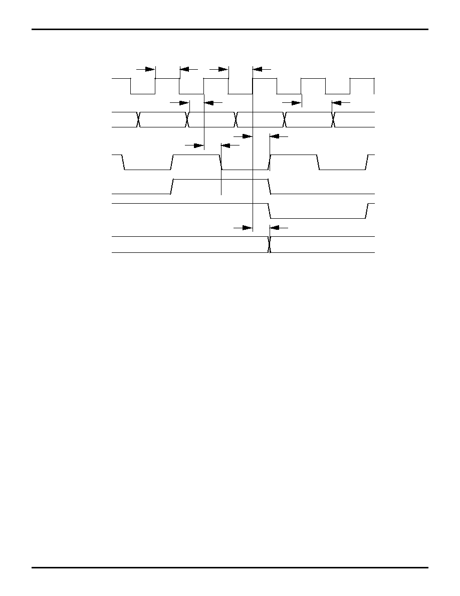
1. The number of TXIFCLK cycles per cycle of TXCHPPLS is determined by the data stored in bits 5-0 of address 41
H
. It is shown
as 2 in Figure 8 but can be set from 2 to 64.
2. The width of the TXBITPLS, TXTRKPLS and TXACQPLS signal pulses is equal to the period of TXCHPPLS; that is, equal to
the PN chip period.
3. In QPSK mode, the TXBITPLS signal pulses high twice during each symbol period, once during the center chip and once
during the last chip. If the number of chips per symbol is even, the number of chip periods between the TXBITPLS pulse at
the end of the previous symbol and the one in the center of the symbol will be one more than the number of chip periods
between the TXBITPLS pulse in the center of the symbol and the one at the end. The falling edge of the second pulse corre-
sponds to the end of the symbol period.
4. The TXTRKPLS signal pulses high once each symbol period, during the last chip period of that symbol. The falling edge cor-
responds to the end of the symbol period.
5. The TXACQPLS signal pulses high once each burst, transmission, during the last chip of the Acquisition/Preamble symbol.
The falling edge corresponds to the end of this symbol period.
PS010202-0601

Z87200
Spread-Spectrum Transceiver
Zilog
4-10
Figure 4. Transmitter Input/Output Timing
TXIFCLK
TXIN
t
CH
t
CL
t
SU
t
HD
t
CT
t
CT
TXCHPPLS
TXBITPLS,
TXTRKPLS,
TXACQPLS
DON'T CARE
VALID
DON'T CARE
TXIOUT,
TXQOUT
t
CT
TXIFOUT
PS010202-0601

Z87200
Zilog
Spread-Spectrum Transceiver
4-11
4
A.C. CHARACTERISTICS - RECEIVER
Operating Conditions: V
DD
= 5.0V
±
5%, V
SS
= 0V
T
A
= 0
∞
to +70
∞
C
Symbol
Parameter
Min
Max.
Units
Conditions
f
RXIFCLK
RXIFCLK Frequency
45.056
20.0
MHz
MHz
Z8720045FSC
Z8720020FSC
t
CH
RXIFCLK Pulse
width, High
10
ns
t
CL
RXIFCLK Pulse
width, Low
10
ns
t
SU
RXIIN or RXQIN to
RXIFCLK setup
3
ns
t
HD
RXIIN or RXQIN to
RXIFCLK hold
7
ns
t
CR
RXIFCLK to
RXSPLPLS,
RXSYMPLS, or
/RXDRDY delay
35
ns
t
CD
RXIFCLK to RXOUT,
RXIOUT, or
RXQOUT delay
35
ns
Notes:
1. The number of RXIFCLK cycles per cycle of RXSPLPLS is determined by the data stored in bits 5-0
of address 02
H
. It is shown as 2 in Figure 9, but can be set from 2 to 64.
2. The rising edge of /RXDRDY should be used to clock out the data (RXOUT, RXIOUT, or RXQOUT).
PS010202-0601
Z87200
Spread-Spectrum Transceiver
Zilog
4-12
A.C. CHARACTERISTICS
Figure 5. Receiver Input/Output
RXIFCLK
RXIIN,
RXQIN
RXSPLPLS
RXSYMPLS
t
CH
t
CL
t
SU
t
HD
t
CR
t
CR
t
CD
/RXDRDY
RXOUT,
RXIOUT,
RXQOUT
PS010202-0601
Z87200
Zilog
Spread-Spectrum Transceiver
4-13
4
AC CHARACTERISTICS
Operating Conditions: V
DD
= 5.0V
±
5%, V
SS
= 0V
T
A
= 0
∞
to +70
∞
C
Symbol
Parameter
Min
Max
Units
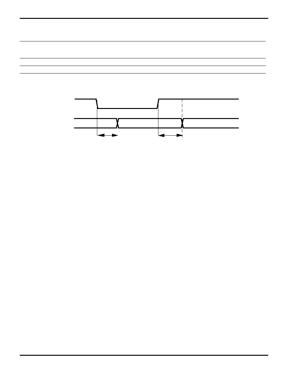
t
D1
/OEN low to RXTEST
7-0
active
11
ns
t
D2
/OEN high to RXTEST
7-0
tri-state
7
ns
Figure 6. /OEN to RXTEST 7-0 Timing
RXTEST 7-0
/OEN
TD1
TD2
Tri-state
Low Impedance State
Tri-state
PS010202-0601

Z87200
Spread-Spectrum Transceiver
Zilog
4-14
FUNCTIONAL BLOCKS
Transmit and Receive Clock Generators
Timing in the transmitter and receiver sections of the
Z87200 is controlled by the Transmit and Receive Clock
Generator Blocks. These blocks are programmable divid-
ers providing signals at the chip and symbol rates (as well
as at multiples and sub-multiples of these frequencies) as
programmed through the Z87200's control registers. If de-
sired, the complete independence of the transmitter and
receiver sections allows the transmit and receive clocks to
be mutually asynchronous. Additionally, the Z87200 al-
lows external signals to be provided as references for the
transmit (TXMCHP) and receive (RXMSMPL) chip rates.
Given the transmit PN chip rate, the PN-synchronous
transmit symbol rate is then derived from the programmed
number of PN chips per transmit symbol. At the receiver,
symbol synchronization and the receive symbol rate are
determined from processing of the PN matched filter out-
put, or, if desired, can be provided from the programmed
number of PN chips per receive symbol or an external
symbol synch symbol, RXMDET. Burst control is achieved
by means of the transmit and receive Symbols per Burst
counters. These programmable 16-bit counters allow the
Z87200 to operate automatically in burst mode, stopping
at the end of each burst without the need of any external
counters.
Input and Output Processors
When the transmitter and receiver are operating in QPSK
mode, the data to be transmitted and the received data are
processed in pairs of bits (dibits), one bit for the in-phase
(I) channel and one for the quadrature (Q) channel. Dibits
are transmitted and received as single differentially encod-
ed QPSK symbols. Single-bit I/O data is converted to and
from this format by the Input and Output Processors, ac-
cepting TXIN as the serial data to be transmitted and pro-
ducing RXOUT as the serial data output. If desired, the re-
ceived data is also available at the RXIOUT and RXQOUT
pins in (I and Q) dibit format prior to dibit-to-serial conver-
sion. While receive timing is derived by the Z87200 Sym-
bol Tracking Processor, transmit timing is provided by the
Input Processor. In BPSK mode, the Input Processor will
generate the TXBITPLS signal once per symbol to request
each bit of data, while in QPSK mode it will generate the
TXBITPLS signal twice per symbol to request the two bits
of data corresponding to each QPSK symbol.
Differential Encoder
Data to be transmitted is differentially encoded before be-
ing spread by the transmit PN code. Differential encoding
of the signal is fundamental to operation of the Z87200's
receiver: the Z87200's DPSK Demodulator computes
"Dot" and "Cross" product functions of the current and pre-
vious symbols' downconverted I and Q signal components
in order to perform differential decoding as an intrinsic part
of DPSK demodulation.
The differential encoding scheme depends on whether the
modulation format is to be BPSK or QPSK. For DBPSK,
the encoding algorithm is straightforward: output bit(k)
equals input bit(k)
output bit(k≠1), where
represents
the logical XOR function. For DQPSK, however, the differ-
ential encoding algorithm, as shown in Table 2, is more
complex since there are now sixteen possible new states
depending on the four possible previous output states and
four possible new input states.
Table 2. QPSK Differential Encoder Sequence
New Input
Previously Encoded OUT(I,Q)
K-1
IN(I,Q)
K
0
0
0
1
1
1
1
0
0
0
0
0
0
1
1
1
1
0
0
1
0
1
1
1
1
0
0
0
1
1
1
1
1
0
0
0
0
1
1
0
1
0
0
0
0
1
1
1
Newly Encoded OUT (I,Q)K
PS010202-0601

Z87200
Zilog
Spread-Spectrum Transceiver
4-15
4
Transmitter PN Code Generation
When the Z87200 is used for burst signal operation, each
burst is preceded by an Acquisition/Preamble symbol to
facilitate acquisition. This Acquisition/Preamble symbol is
automatically generated by the Z87200's transmitter be-
fore information data symbols are accepted for transmis-
sion. Two separate and independent PN codes may be
employed: one for spreading the Acquisition/Preamble
symbol, and one for the subsequent information data sym-
bols. As a result, a much higher processing gain may be
used for signal acquisition than for signal tracking in order
to improve burst acquisition performance.
The Transmitter Acquisition/Preamble and Transmitter
Data Symbol PN code lengths are completely independent
of each other and can be up to 64 chips long. Transmit PN
codes are programmed in the Z87200 as binary code val-
ues. The number of Transmitter Chips per Acquisition/Pre-
amble Symbol is set by the value stored in bits 5-0 of ad-
dress 43
H
, and the Transmitter Acquisition/Preamble
Symbol Code coefficient values are stored in addresses
44
H
to 4B
H
. The number of Transmitter Chips per Data
Symbol is set by the data stored in address 42
H
, and the
Transmitter Data Symbol Code coefficient values are
stored in addresses 4C
H
to 53
H
.
A rising edge of the MTXEN input or of bit 1 of address 37
H
causes the Z87200 to begin the transmit sequence by
transmitting a single symbol using the Acquisition/Pream-
ble PN code. The completion of transmission of the Acqui-
sition/Preamble symbol is indicated with TXACQPLS,
while the ongoing transmission of data symbols is signaled
with TXTRKPLS. Data bits to be transmitted after the Ac-
quisition/Preamble symbol are requested with TXBITPLS,
where a single pulse requests data in BPSK mode and two
pulses request data in QPSK mode. The user data sym-
bols are then PN modulated using the Transmitter Data
Symbol PN code.
The PN spreading codes are XORed with the data bits (in
BPSK mode) or bit pairs (in QPSK mode) to transmit one
complete code sequence for every Acquisition/Preamble
and data symbol at all times. The resulting spread I and Q
channel signals are brought out as the TXIOUT and TX-
QOUT signals for use by an external modulator and are
also fed into the Z87200's internal on-chip modulator. In
BPSK mode, only TXIOUT is used by the Z87200's modu-
lator. If an external QPSK modulator is used, the carrier
should be modulated as shown in Table 3 to be compatible
with the Z87200 receiver.
BPSK/QPSK Modulator
The Z87200 incorporates an on-chip BPSK/QPSK modu-
lator which modulates the encoded and spread transmit
signal with the sine and cosine outputs of the Z87200's
NCO to generate a digitized I.F. output signal, TXIFOUT
7-
0
. Since the NCO operates at a rate defined by RXIFCLK,
the BPSK/QPSK modulator output is also generated at this
sampling rate, and, consequently, TXIFCLK must be held
common with RXIFCLK to operate the Z87200's
BPSK/QPSK Modulator. The digital modulator output sig-
nal can then be fed into an external 8-bit DAC (operating
at RXIFCLK) to generate an analog I.F. transmit signal,
where the chosen I.F. is the Z87200's programmed NCO
frequency or one of its aliases with respect to the output
sampling rate, RXIFCLK. Please note that operation of the
BPSK/QPSK modulator is only specified to 20 MHz; that is,
if RXIFCLK/TXIFCLK is greater than 20 MHz in the system
design, it is recommended that the baseband transmit out-
puts of the Z87200 be used with an external BPSK/QPSK
modulator.
When the Z87200 is set to transmit in BPSK mode (by set-
ting bit 0 of address 40
H
high), identical signals are applied
to both the I and Q channels of the modulator so that the
modulated output signal occupies only the first and third
quadrants of the signal space defined in Note that the
modulator itself cannot generate
/4 QPSK signals, but the
Z87200 can receive such signals and can be used with an
external modulator for their transmission.
Table 3. DQPSK Differential Encoder Sequence
I, Q BIts
Signal
Quadrant
Quadrant Diagram
0
0
First
2nd
1st
1
0
Second
3rd
4th
1
1
Third
0
1
Fourth
PS010202-0601

Z87200
Spread-Spectrum Transceiver
Zilog
4-16
FUNCTIONAL BLOCKS (Continued)
Frequency Control Register and NCO
The Z87200 incorporates a Numerically Controlled Oscil-
lator (NCO) to synthesize a local oscillator signal for both
the transmitter's modulator and receiver's downconverter.
The NCO is clocked by the master receiver clock signal,
RXIFCLK, and generates quadrature outputs with 32-bit
frequency resolution. The NCO frequency is controlled by
the value stored in the 32-bit Frequency Control Register,
occupying 4 bytes at addresses 03
H
to 06
H
. To avoid de-
structive in-band aliasing, the NCO should not be pro-
grammed to be greater than 50% of RXIFCLK. As desired
by the user, the output of the Z87200 receiver's Loop Filter
can then be added or subtracted to adjust the NCO's fre-
quency control word and create a closed-loop frequency
tracking loop. If the receiver is disabled, either manually or
automatically at the end of a burst, the Loop Filter output
correcting the NCO's Frequency Control Word is disabled.
When simultaneously operating both the transmitter and
receiver, however, the receiver's frequency tracking loop
affects the NCO signals to both the receive and transmit
sides, a feature which can either be used to advantage in
the overall system design or must be compensated in the
programming of the Z87200 or in the system design.
Downconverter
The Z87200 incorporates a Quadrature (Single Sideband)
Downconverter which digitally downconverts the sampled
and digitized receive I.F. signal to baseband. Use of the
Loop Filter and the NCO's built-in frequency tracking loop
permits the received signal to be accurately downconvert-
ed to baseband.
The Downconverter includes a complex multiplier in which
the 8-bit receiver input signal is multiplied by the sine and
cosine signals generated by the NCO. In Quadrature Sam-
pling Mode, two ADCs provide quadrature (complex) in-
puts I
IN
and Q
IN
, while, in Direct I.F. Sampling Mode, a sin-
gle ADC provides I
IN
as a real input. The input signals can
be accepted in either two's complement or offset binary
formats according to the setting of bit 3 of address 01
H
. In
Direct I.F. Sampling Mode, the unused RXQIN Q channel
input (Q
IN
) should be held to "zero" according to the ADC
input format selected. The outputs of the Downconverter's
complex multiplier are then:
I
OUT
=
I
IN
. cos(
t) ≠
Q
IN
. sin(
t)
Q
OUT
=
I
IN
. s
in
(
t) +
Q
IN
. cos(
t)
where
=
2
f
nco
These outputs are fed into the I and Q channel Integrate
and Dump Filters. The Integrate and Dump Filters allow
the samples from the complex multiplier (at the I.F. sam-
pling rate, the frequency of RXIFCLK) to be integrated over
a number of sample periods. The dump rate of these filters
(the baseband sampling rate) can be controlled either by
an internally generated dump clock or by an external input
signal (RXMSMPL) according to the setting of bit 0 of ad-
dress 01
H
. Note that, while the receiver will extract exact
PN and symbol timing information from the received sig-
nal, the baseband sampling rate must be twice the nominal
PN chip rate for proper receiver operation and less than or
equal to one-half the frequency of RXIFCLK. If twice the
PN chip rate is a convenient integer sub-multiple of RXIF-
CLK, then an internal clock can be derived by frequency di-
viding RXIFCLK according to the divisor stored in bits 5-0
of address 02
H
; otherwise, an external baseband sampling
clock provided by RXMSMPL must be used.
The I.F. sampling rate, the baseband sampling rate, and
the input signal levels determine the magnitudes of the In-
tegrate and Dump Filters' accumulator outputs, and a pro-
grammable viewport is provided at the outputs of the Inte-
grate and Dump Filters to select the appropriate output bits
as the 3-bit inputs to the PN Matched Filter. The viewport
circuitry here and elsewhere within the Z87200's receiver
is designed with saturation protection so that extreme val-
ues above or below the selected range are limited to the
correct maximum or minimum value for the selected view-
port range. Both viewports for the I and Q channels of the
Integrate and Dump Filters are controlled by the values
stored in bits 7-4 of address 01
H
.
Receiver PN Code Register and PN Matched
Filter
As discussed for the Z87200 transmitter, the Z87200 re-
ceiver is designed for burst signal operation in which each
burst begins with a single Acquisition/Preamble symbol
and is then followed by data symbols for information trans-
mittal. Complementing operation of the Z87200's transmit-
ter, two separate and independent PN codes may be em-
ployed in the receiver's PN Matched Filter, one for
despreading the Acquisition/Preamble symbol, and one for
the information data symbols. The code lengths are com-
pletely independent of each other and can be each up to
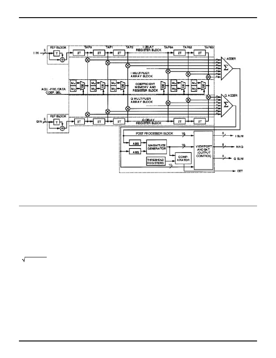
64 chips long. A block diagram of the PN Matched Filter is
shown in Figure 3.
PS010202-0601

Z87200
Spread-Spectrum Transceiver
Zilog
4-17
The Z87200 contains a fully programmable 64-tap com-
plex (dual I and Q channel) PN Matched Filter with coeffi-
cients which can be set to
±
1 or zero according to the con-
tents of either the Acquisition/Preamble or Data Symbol
Code Coefficient Registers. By setting the coefficients of
the end taps of the filter to zero, the effective length of the
filter can be reduced for use with PN codes shorter than 64
bits. Power consumption may also be reduced by turning
off those blocks of 7 taps for which all the coefficients are
zero, using bits 6-0 of address 39H. Each ternary coeffi-
cient is stored as a 2-bit number so that a PN code of
length N is stored as N 2-bit non-zero PN coefficients. Note
that, as a convention, throughout this document the first
PN Matched Filter tap encountered by the signal as it en-
ters the I and Q channel tapped delay lines is referred to
as "Tap 0." Tap 63 is then the last tap of the PN Matched
Filter.
The start of each burst is expected to be a single symbol
PN-spread by the Acquisition/Preamble code. The receiv-
er section of the Z87200 is automatically configured into
acquisition mode so that the Matched Filter Acquisi-
tion/Preamble Coefficients stored in addresses 07
H
to 16
H
are used to despread the received signal. Provided that
this symbol is successfully detected, the receiver will auto-
matically switch from acquisition mode, and the Matched
Filter Data Symbol Coefficients stored in addresses 17
H
to
26
H
will then be used to despread subsequent symbols.
To allow the system to sample the incoming signal asyn-
chronously (at the I.F. sampling rate) with respect to the
PN spreading rate, the PN Matched Filter is designed to
operate with two signal samples (at the baseband sam-
pling rate) per chip. A front end processor (FEP) operating
on both the I and Q channels averages the incoming data
over each chip period by adding each incoming baseband
sample to the previous one:
FEP
OUT
= FEP
IN
(1 + z
≠1
)
After the addition, the output of the FEP is rounded to a 3-
bit offset 2's complement word with an effective range of
±
3.5 such that the rounding process does not introduce
any bias to the data. The FEP can be disabled by setting
bit 0 of address 27
H
to 1, but for normal operation the FEP
should be enabled.
The PN Matched Filter computes the cross-correlation be-
tween the I and Q channel signals and the locally stored
PN code coefficients at the baseband sampling rate, which
is twice per chip. The 3-bit signals from each tap in the PN
Matched Filter are multiplied by the corresponding coeffi-
cient in two parallel tapped delay lines. Each delay line
consists of 64 multipliers which multiply the delayed
3-bit signals by zero or
±
1 according to the value of the tap
coefficient. The products from the I and Q tapped delay
lines are added together in the I and Q Adders to form the
sums of the products, representing the complex cross-cor-
relation factor. The correlation I and Q outputs are thus:
n = 63
Output
(I, Q)
=
Data
n(I, Q)
* Coefficient
n(I, Q)
n = 0
These I and Q channel PN Matched Filter outputs are 10-
bit signals, with I and Q channel programmable viewports
provided to select the appropriate output bits as the 8-bit
inputs to the Power Detector and DPSK Demodulator
blocks. Both I and Q channel viewports are jointly con-
trolled by the data stored in bits 1-0 of address 28
H
and are
saturation protected.
Two power saving methods are used in the PN Matched
Filter of the Z87200. As discussed previously, the first
method allows power to be shut off in the unused taps of
the PN Matched Filter when the filter length is configured
to be less than 64 taps. The second method is a propri-
etary technique that (transparently to the user) shuts down
the entire PN Matched Filter during portions of each sym-
bol period.
PS010202-0601
Z87200
Spread-Spectrum Transceiver
Zilog
4-18
FUNCTIONAL BLOCKS (Continued)
Power Detector
The complex output of the PN Matched Filter is fed into a
Power Detector which, for every cycle of the internal base-
band sampling clock, computes the magnitude of the vec-
tor of the I and Q channel correlation sums,
I
2
(K)+Q
2
(k), where the magnitude is approximated as
Max{Abs(I),Abs(Q)} + 1/2 Min{Abs(I), Abs(Q)}.
This 10-bit value represents the power level of the corre-
lated signal during each chip period and is used in the
Symbol Tracking Processor.
Symbol Tracking Processor
The output of the Power Detector Block represents the sig-
nal power during each chip period. Ideally, this output will
have a high peak value once per symbol (that is, once per
PN code cycle) when the code sequence of the received
signal in the PN Matched Filter is the same as (and is
aligned in time with) the reference PN code used in the PN
Matched Filter. At that instant, the I and Q channel outputs
of the PN Matched Filter are, theoretically, the optimally
despread I and Q symbols.
Figure 7. PN Matched Filter
PS010202-0601

Z87200
Zilog
Spread-Spectrum Transceiver
4-19
4
To detect this maximum correlation in each symbol period,
the signal power value is compared against a 10-bit user-
programmable threshold value. A symbol clock pulse is
generated each time the power value exceeds the thresh-
old value to indicate a symbol detect. Since the Acquisi-
tion/Preamble symbol and subsequent data symbols can
have different PN codes with different peak correlation val-
ues (which depend on the PN code length and code prop-
erties), the Z87200 is equipped with two separate thresh-
old registers to store the Acquisition/Preamble Threshold
value (stored in addresses 29
H
and 2A
H
) and the Data
Symbol Threshold value (stored in addresses 2B
H
and
2C
H
). The device will automatically use the appropriate
value depending on whether it is in acquisition mode or
not.
Since spread-spectrum receivers are frequently designed
to operate under extremely adverse signal-to-noise ratio
conditions, the Z87200 is equipped with a "flywheel circuit"
to enhance the operation of the symbol tracking function
by introducing memory to the PN Matched Filter operation.
This circuit is designed to ignore false detects at inappro-
priate times in each symbol period and to insert a symbol
clock pulse at the appropriate time if the symbol detection
is missed. The flywheel circuit operates by its
a priori
knowledge of when the next detect pulse is expected.
A
priori, the expected pulse will occur one symbol period af-
ter the last correctly detected one, and a window of
±
1
baseband sample time is therefore used to gate the detect
pulse. Any detects generated outside this time window are
ignored, while a symbol detect pulse will be inserted into
the symbol clock stream if the power level does not exceed
the threshold within the window, corresponding to a
missed detect. An inserted symbol detect signal will be
generated precisely one symbol after the last valid detect,
the nominal symbol length being determined by the value
of Rx Chips Per Data Symbol stored in address 2D
H
.
The cross-correlation characteristics of a noisy received
signal with the noise-free local PN code used in the
Z87200's PN Matched Filter may result in "smearing" of
the peak power value over adjacent chip periods. Such
smearing can result in two or three consecutive power val-
ues (typically, the on-time and one-sample early and late
values) exceeding the threshold. A maximum power selec-
tor circuit is incorporated in the Z87200 to choose the high-
est of any three consecutive power levels each time this
occurs, thereby enhancing the probability that the optimum
symbol timing will be chosen in such cases. If desired, this
function can be disabled by setting bit 3 of address 30
H
high.
The Z87200 also includes a circuit to keep track of missed
detects; that is, those cases where no peak power level ex-
ceeds the set threshold. An excessively high rate of
missed detects is an indication of poor signal quality and
can be used to abort the reception of a burst of data. The
number of symbols expected in each receive burst, up to a
maximum of 65,533, is stored in addresses 2E
H
and 30
H
.
A counter is used to count the number of missed detects in
each burst, and the system can be configured to automat-
ically abort a burst and return to acquisition mode if this
number exceeds the Missed Detects per Burst Threshold
value stored in address 2F
H
. Under normal operating con-
ditions, the Z87200 will automatically return to acquisition
mode when the number of symbols processed in the burst
is equal to the value of the data stored in address 2E
H
and
30
H
. To permit the processing of longer bursts or continu-
ous data, this function can be disabled by setting bit 6 of
address 30
H
high.
Differential Demodulator
Both DPSK demodulation and carrier discrimination are
supported in the Z87200 receiver by the calculation of
"Dot" and "Cross" products using the despread I and Q
channel information generated by the PN Matched Filter
for the current and previous symbols. A block diagram of
the DPSK Demodulator's I and Q channel processing is
shown in Let I
k
and Q
k
represent the I and Q channel out-
puts, respectively, for the k
th
symbol. The Dot and Cross
products can then be defined as:
Dot(k)
= I
k
I
k-1
+ Q
k
Q
k-1
; and,
Cross(k) = Q
k
I
k-1
- I
k
Q
k-1
.
Examination of these products in the complex plane re-
veals that the Dot and Cross products are the real and
imaginary results, respectively, of complex multiplication
of the current and previous symbols. The Dot product
alone thus allows determination of the phase shift between
successive BPSK symbols, while the Dot and Cross prod-
ucts together allow determination of the integer number of
/2 phase shifts between successive QPSK symbols. Dif-
ferential encoding of the source data implies that an abso-
lute phase reference is not required, and thus knowledge
of the phase shift between successive symbols derived
from the Dot and Cross products unambiguously permits
correct demodulation.
Implementation of this approach is simplified if the polari-
ties (the signs) alone of the Dot and Cross products pro-
vide the information required to make the correct symbol
decision. For BPSK and
/4 QPSK signals, no modifica-
tions are needed: in BPSK, the sign of the Dot product fully
captures the signal constellation, while, in
/4 QPSK, the
signal constellation intrinsically includes the phase rotation
needed to align the decision boundaries with the four pos-
sible combinations of the Dot and Cross product polarities.
For QPSK signals, a fixed phase rotation of
/4 (45
∞
) is in-
troduced in the DPSK Demodulator to the previous symbol
to simplify the decision algorithm. Rotation of the previous
symbol is controlled by the settings of bits 0 and 1 of ad-
dress 33
H
, allowing the previous symbol to be rotated by
0
∞
or
±
45
∞
. As noted, for BPSK or
/4 QPSK signals, a ro-
tation of 0
∞
should be programmed, but, for QPSK signals,
PS010202-0601

Z87200
Spread-Spectrum Transceiver
Zilog
4-20
FUNCTIONAL BLOCKS (Continued)
a ≠45
∞
signal rotation must be programmed to optimize the
constellation boundaries in the comparison process be-
tween successive symbols. Note also that introduction of a
±
45
∞
rotation introduces a scaling factor of 1/
2 to the sig-
nal level in the system as discussed in Theory of Opera-
tion, where this factor should be taken into account when
calculating optimum signal levels and viewport settings af-
ter the DPSK Demodulator
Frequency Discriminator and Loop Filter
The Frequency Discriminator uses the Dot and Cross
products discussed above to generate the AFC signal for
the frequency acquisition and tracking loop, as illustrated
in The specific algorithm used depends on the signal mod-
ulation type and is controlled by the setting of bit 2 of ad-
dress 33
H
. When bit 2 is set low, the Frequency Discrimi-
nator circuit is in BPSK mode and the following algorithm
is used to compute the Frequency Discriminator (FD) func-
tion:
FD = Cross x Sign[Dot],
where Sign[.] represents the polarity of the argument.
When bit 2 is set high, the discriminator circuitry is in
QPSK mode and the carrier discriminator function is in-
stead calculated as:
FD = (Cross x Sign[Dot]) ≠ (Dot x Sign[Cross]).
In both cases, the Frequency Discriminator function pro-
vides an error signal that reflects the change in phase be-
tween successive symbols. With the symbol period known,
the error signal can equivalently be seen as a frequency
error signal. As a practical matter, the computation of the
Frequency Discriminator function results in a 17-bit signal,
and a programmable saturation protected viewport is pro-
vided to select the desired output bits as the 8-bit input to
the Loop Filter Block. The viewport is controlled by the val-
ue stored in bits 7-4 of address 33
H
.
The Loop Filter is implemented with a direct gain (K1) path
and an integrated or accumulated (K2) path to filter the
Frequency Discriminator error signal and correct the fre-
quency tracking of the Downconverter. The order of the
Loop Filter transfer function can be set by enabling or dis-
abling the K1 and K2 paths, and the coefficient values can
be adjusted in powers of 2 from 2
0
to 2
21
. The Loop Filter
transfer function is:
Transfer Fn. = K1 + 1/4 K2
Figure 8. DPSK Demodulator I and Q Channel Processing
PS010202-0601

Z87200
Zilog
Spread-Spectrum Transceiver
4-21
4
The factor of 1/4 results from truncation of the 2 LSBs of
the signal in the integrator path of the loop so that, when
added to the signal in the direct path, the LSBs of the sig-
nals are aligned. The coefficients K1 and K2 are defined by
the data stored in bits 4-0 of addresses 35
H
and 34
H
, re-
spectively. In addition, bit 5 of addresses 35
H
and 34
H
con-
trol whether the K1 and K2 paths, respectively, are en-
abled. These parameters thus give the user full control of
the Loop Filter characteristics.
RXIIN
7-0
(Pins 91-98)
Receiver In-Phase Input. RXIIN is an 8-bit input port for
in-phase data from external A/D converters. Data may be
received in either two's complement or offset binary format
as selected by bit 3 of address 01
H
. The sampling rate of
the RXIIN signals (the I.F. sampling rate of the A/Ds) may
be independent of the baseband sampling rate (the Down-
converter integrate and dump rate) and the PN chip rate,
but must be equal to RXIFCLK and at least two times
greater than the baseband sampling rate. Since the base-
band sampling rate must be set at twice the PN chip rate,
the I.F. sampling rate must thus be at least four times the
PN chip rate. Data on the pins is latched and processed by
RXIFCLK.
RXQIN
7-0
(Pins 2-9)
Receiver Quadrature-Phase Input. RXQIN is an 8-bit in-
put port for quadrature-phase data from external A/D con-
verters. Data may be received in either two's complement
or offset binary format as selected by bit 3 of address 01
H
.
As with RXIIN, the sampling rate of the RXQIN signals may
be independent of the baseband sampling and PN chip
rates in the receiver, but must be at least two times greater
than the baseband sample rate (or, equivalently, at least
four times greater than the PN chip rate). Data on the pins
is latched and processed by RXIFCLK.
Figure 9. Frequency Discriminator and Loop Filter Detail
PS010202-0601

Z87200
Spread-Spectrum Transceiver
Zilog
4-22
FUNCTIONAL BLOCKS (Continued)
Note that if the Z87200 is to be used in Direct I.F. Sampling
Mode, then the I.F. signal should be input to the RXIIN in-
put port only. RXQIN must then be held to arithmetic zero
according to the chosen ADC format as selected by bit 3
of address 01
H
. In other words, to support Direct I.F. Sam-
pling, RXQIN must be tied to a value of 127 or 128 if offset
binary input format has been selected or to a value of 0 if
two's complement input format has been selected.
RXMSMPL (Pin 84)
Receiver Manual Sample Clock. RXMSMPL enables the
user to externally generate (independent of the I.F. sam-
pling clock, RXIFCLK) the baseband sampling clock used
for all processing after the digital downconverter, including
the dump rate of the Integrate and Dump filters. This fea-
ture is useful in cases where a specific baseband sample
rate is required that may not be derived by the internal
sample rate timing generator which generates clock sig-
nals at integer sub-multiples of RXIFCLK. The signal is in-
ternally synchronized to RXIFCLK to avoid intrinsic race or
hazard timing conditions. There must be at least two cy-
cles of RXIFCLK to every cycle of RXMSMPL, and
RXMSMPL should be set to twice the nominal receive PN
chip rate.
When bit 0 of address 01
H
is set high, a rising edge on
RXMSMPL will initiate a baseband sampling clock pulse to
the Integrate and Dump filters and subsequent circuitry
(e.g., PN Matched Filter, DPSK Demodulator, Power Esti-
mator, etc.). The rising edge of RXMSMPL is synchronized
internally so that, on the second rising edge of RXIFCLK
that follows the rising edge of RXMSMPL, a pulse is inter-
nally generated that clocks the circuitry that follows. On the
third rising RXIFCLK edge, the contents of the Integrate
and Dump Filters of the Downconverter are transferred to
the PN Matched Filter. The extra one RXIFCLK delay be-
fore transfer of the contents of the filters enables the inter-
nally generated baseband sampling clock to be free of
race conditions at the interface between the Downconvert-
er and PN Matched Filter.
RXMDET (Pin 88)
Receiver Manual Detect. RXMDET enables the user to
externally generate symbol timing, bypassing and overrid-
ing the internal symbol power estimation and tracking cir-
cuitry. This function may be useful when the dynamic char-
acteristics of the transmission environment require
unusual adjustments to the symbol timing.
When bit 0 of address 30
H
is set high (Manual Detect En-
able) and when bit 0 of address 31
H
is set low, a rising
edge of RXMDET will generate a symbol correlation detect
pulse. The function can also be performed by means of bit
0 of address 31
H
. The RXMDET input and bit 0 of address
31
H
are logically ORed together so that, when either one
is held low, a rising edge on the other triggers the manual
detect function. The rising edge of RXMDET is synchro-
nized internally so that, on the second rising edge of the
baseband sampling clock that follows the rising edge of
RXMDET, the correlated outputs of the PN Matched Filter
I and Q channels will be transferred to the DPSK demodu-
lator.
RXMABRT (Pin 87)
Receiver Manual Abort. RXMABRT enables the user to
manually force the Z87200 to cease reception of the cur-
rent burst of data symbols and prepare for acquisition of a
new burst. This function can be used to reset the receiver
and prepare to receive a priority transmission signal under
precise timing control, giving the user the ability to control
the current status of the receiver for reasons of priority, sig-
nal integrity, etc.
When bit 0 of address 32
H
is set low, a rising edge on
RXMABRT will execute the abort function. The function
can also be performed under microprocessor control by
means of bit 0 of address 32
H
. The RXMABRT input and
bit 0 of address 32
H
are logically ORed together so that,
when either one is held low, a rising edge on the other trig-
gers the abort function. The second rising edge of the
baseband sampling clock that follows a rising edge of
RXMABRT will execute the abort and also clear the sym-
bols-per-burst, samples-per-symbol, and missed-detects-
per-burst counters. The counters will be reactivated on the
detection of the next burst preamble or by a manual detect
signal.
RXIFCLK (Pin 12)
Receiver I.F. Clock. RXIFCLK is the master clock of the
NCO and all the receiver blocks. All clocks in the receiver
section and the NCO, internal or external, are generated or
synchronized internally to the rising edge of RXIFCLK. The
frequency of RXIFCLK must be at least four times the PN
chip rate of the received signal. When bit 0 of address 01
H
is set low, the baseband sampling clock, required to be at
twice the nominal PN chip rate, will be derived from RXIF-
CLK according to the setting of bits 5-0 of address 02
H
.
MNCOEN (Pin 86)
Manual NCO Enable. MNCOEN allows the power con-
sumed by the operation of the NCO circuitry to be mini-
mized when the Z87200 is not receiving and not transmit-
ting data. The NCO can also be disabled while the Z87200
is transmitting as long as the Z87200's on-chip
BPSK/QPSK modulator is not being used. With the instan-
taneous acquisition properties of the PN Matched Filter, it
is often desirable to shut down the receiver circuitry to re-
duce power consumption, resuming reception periodically
until an Acquisition/Preamble symbol is acquired. Setting
MNCOEN low holds the NCO in a reset state; setting MN-
COEN high then reactivates the NCO, where it is neces-
sary to then reload the frequency control word into the
PS010202-0601

Z87200
Zilog
Spread-Spectrum Transceiver
4-23
4
NCO. Note that MNCOEN operates independently of
MTXEN and MRXEN, where those pins have similar con-
trol over the transmit and receive circuitry, respectively.
MNCOEN performs the same function as bit 0 of address
37
H
, and these two signals are logically ORed together to
form the overall control function. When bit 0 of address 37
H
is set low, MNCOEN controls the activity of the NCO cir-
cuitry; when MNCOEN is set low, bit 0 of address 37
H
con-
trols the activity of the NCO circuitry. When either bit 0 or
MNCOEN (whichever is in control, as defined above) goes
low, a reset sequence occurs on the following RXIFCLK
cycle to effectively disable all of the NCO circuitry, al-
though the user programmable control registers are not af-
fected by this power down sequence.
Upon reactivation (when either MNCOEN or bit 0 of ad-
dress 37
H
return high), the NCO must be reloaded with fre-
quency control information either by means of the MFLD
input or by writing 01
H
into address 00
H
.
MTXEN (Pin 17)
Manual Transmitter Enable. A rising edge on MTXEN
causes the transmit sequence to begin, where the Z87200
first transmits a single Acquisition/Preamble symbol fol-
lowed by data symbols. MTXEN should be set low after the
last symbol has been transmitted. When MTXEN is set
low, power consumption of the transmitter circuit is mini-
mized. MTXEN operates independently of MRXEN and
MNCOEN, where these signals have similar control over
the receive and NCO circuitry, respectively.
MTXEN performs the same function as bit 1 of address
37
H
. and these two signals are logically ORed together to
form the overall control function. When bit 1 of address 37
H
is set low, MTXEN controls the activity of the transmitter
circuitry, and, when MTXEN is set low, bit 1 of address 37H
controls the activity of the transmitter circuitry. A rising
edge on either MTXEN or bit 1 (whichever is in control, as
defined above) initiates a transmit sequence. A falling
edge initiates a reset sequence on the following TXIFCLK
cycle to disable all of the transmitter data path, although
the user programmable control registers are not affected
by the power down sequence.
MRXEN (Pin 10)
Manual Receiver Enable. MRXEN allows power con-
sumption of the Z87200 receiver circuitry to be minimized
when the device is not receiving. With the instantaneous
acquisition properties of the PN Matched Filter, it is often
desirable to shut down the receiver circuitry to reduce pow-
er consumption, resuming reception periodically until an
Acquisition/Preamble symbol is acquired. Setting MRXEN
low reduces the power consumption substantially. When
MRXEN is set high, the receiver will automatically power
up in acquisition mode regardless of its prior state when it
was powered down. MRXEN operates independently of
MTXEN and MNCOEN, where these signals have similar
control over the transmit and NCO circuitry, respectively.
MRXEN performs the same function as bit 2 of address
37
H
, and these two signals are logically ORed together to
form the overall control function. When bit 2 of address 37
H
is set low, MRXEN controls the activity of the receiver cir-
cuitry and, when MRXEN is set low, bit 2 of address 37
H
controls the activity of the receiver circuitry. When either
MRXEN or bit 2 (whichever is in control, as defined above)
goes low, a reset sequence begins on the following RXIF-
CLK cycle and continues through a total of six RXIFCLK
cycles to virtually disable all of the receiver data paths. The
user-programmable control registers are not affected by
the power-down sequence, with the exception of
RXTEST
7-0
Function Select (address 38
H
), which is reset
to 0. If the RXTEST
7-0
bus is being used to read any func-
tion other than the PN Matched Filter I and Q inputs, the
value required must be rewritten after re-enabling the re-
ceiver.
TXIN (Pin 18)
Transmit Input. TXIN supports input of the information
data to be transmitted by the Z87200. In BPSK mode, the
transmitter requires one bit per symbol period; in QPSK
mode, two bits are required per symbol period.
To initiate and enable transmission of the data, the user
must raise MTXEN high. Data for transmission is request-
ed with TXBITPLS, where one or two pulses per symbol
are generated depending on whether the device is in
BPSK or QPSK mode as set by bit 0 of address 40
H
. To al-
low monitoring of the state of the transmitter, the Z87200
will pulse TXACQPLS after the initial Acquisition/Preamble
symbol is transmitted; the transmission of each subse-
quent symbol is indicated by pulses of TXTRKPLS.
If programmed for BPSK mode, data is requested by the
Z87200 by a rising edge of output signal TXBITPLS, where
TKBITPLS is generated once per symbol, one chip period
before the end of the current symbol. At the end of the sym-
bol duration, the TXIN data is latched into the device. TX-
BITPLS falls low immediately following the rising edge of
TXIFCLK, which latches the TXIN value, and is generated
repeatedly at the symbol rate as long as the input signal
MTXEN remains high.
In QPSK mode, data is requested by the Z87200 by a ris-
ing edge of output signal TXBITPLS, where this signal is
generated twice per symbol, first one chip period before
the middle of the symbol and then one chip period before
the end of the symbol. TXBITPLS requests the data exact-
ly one chip cycle before latching the TXIN data into the de-
vice. TXBITPLS falls low immediately following the rising
edge of TXIFCLK, which latches the TXIN value.
PS010202-0601

Z87200
Spread-Spectrum Transceiver
Zilog
4-24
FUNCTIONAL BLOCKS (Continued)
TXMCHP (Pin 19)
Transmit Manual Chip Pulse. TXMCHP enables the user
to provide the PN chip rate clock pulses from an external
source. This feature is useful in cases where a specific
chip rate is required that cannot be derived by the internal
clock generator which generates clocks of integer sub-
multiples of TXIFCLK. The signal is internally synchro-
nized to TXIFCLK to avoid intrinsic race or hazard timing
conditions.
When bit 2 of address 40
H
is set high, a rising edge on
TXMCHP will generate the chip clock to the differential en-
coder and the following circuitry (Acquisition/Preamble
and Data Symbol PN spreaders, etc.). The rising edge of
TXMCHP is synchronized internally so that, on the third
rising edge of TXIFCLK following the rising edge of TXM-
CHP, the PN code combined with the differentially encod-
ed signal will change, generating the next chip.
TXIFCLK (Pin 14)
Transmitter I.F. Clock. TXIFCLK is the master clock of
the transmitter. All transmitter clocks, internal or external,
are generated or synchronized internally to the rising edge
of TXIFCLK. The rate of TXIFCLK must be at least twice
the transmit PN chip rate. It may be convenient to use the
same external signal for both TXIFCLK and RXIFCLK, in
which case the frequency of TXIFCLK will be at least four
times the PN chip rate as required for RXIFCLK. Moreover,
if the Z87200's on-chip BPSK/QPSK Modulator is to be
used, TXIFCLK and RXIFCLK must be identical and
should not exceed 20 MHz.
MFLD (Pin 85)
Manual Frequency Load. MFLD is used to load a fre-
quency control value into the NCO. The NCO may be load-
ed in various ways, but MFLD provides a synchronized ex-
ternal method of updating the NCO, while the other
methods involve setting bit 0 of address 00H or using the
programmable loop filter timing circuitry. MFLD is internal-
ly synchronized to RXIFCLK to avoid internal race or haz-
ard timing conditions.
The MFLD input and bit 0 of address 00H are logically
ORed together so that, when either one is held low, a rising
edge on the other triggers the frequency load function
manually. The rising edge of MFLD is synchronized inter-
nally so that, on the sixth following rising edge of RXIF-
CLK, the frequency control word is completely registered
into the NCO accumulator. The frequency load command
must not be repeated until the six RXIFCLK cycle delay is
completed.
/WR (Pin 28)
Write Bar. /WR is used to latch user-configurable informa-
tion into the control registers. It is important to note that the
control registers are transparent latches while /WR is set
low. The information will be latched when /WR returns
high. DATA
7-0
and ADDR
6-0
should be stable while /WR is
set low in order to avoid undesirable effects.
DATA
7-0
(Pins 20-27)
Data Bus. DATA
7-0
is an 8-bit microprocessor interface
bus that provides access to all internal control register in-
puts for programming. DATA
7-0
is used in conjunction with
the ADDR
6-0
and /WR signals to set the values of the con-
trol registers.
ADDR
6-0
(Pins 32-38)
Address Bus. ADDR
6-0
is a 7-bit address bus that selects
the control register location into which the information pro-
vided on the DATA
7-0
bus will be written. ADDR
6-0
is used
in conjunction with /WR and DATA
7-0
to write the informa-
tion into the registers.
/CSEL (Pin 29)
Chip Select Bar. /CSEL is provided to enable or disable
the microprocessor operation of the Z87200. When /CSEL
is set high, the ADDR
6-0
and /WR become disabled and
have no effect on the device. When /CSEL is set low, the
device is in its normal mode of operation and ADDR
6-0
and
/WR are active.
/OEN (Pin 49)
Output Enable Bar. /OEN is provided to enable or disable
the RXTEST
7-0
output bus. When /OEN is set high, the
RXTEST
7-0
bus will have a high impedance, allowing it to
be connected to other busses, such as DATA
7-0
. When
/OEN is set low, the RXTEST
7-0
bus will be active, allowing
the RXTEST function selected to be accessed.
/RESET (Pin 16)
Reset Bar. /RESET is the master reset of the Z87200,
clearing the control registers as well as the contents within
the receiver, transmitter, and NCO data paths when it is
set low. Setting /RESET high enables operation of the cir-
cuitry.
PS010202-0601

Z87200
Zilog
Spread-Spectrum Transceiver
4-25
4
OUTPUT SIGNALS
TXIOUT (Pin 77)
Transmitter In-Phase Output. TXIOUT is the in-phase
output transmission signal that has been differentially en-
coded and PN spread. TXIOUT changes on the rising
edge of TXIFCLK following the falling edge of TXCHPPLS.
TXQOUT (Pin 76)
Transmitter Quadrature-Phase Output. TXQOUT is the
quadrature-phase output transmission signal that has
been differentially encoded and PN spread. TXQOUT
changes on the rising edge of TXIFCLK following the fall-
ing edge of TXCHPPLS.
TXIFOUT
7-0
(Pins 66-73)
Transmitter I.F. Output. TXIFOUT
7-0
is the modulated
transmit output signal from the on-chip BPSK/QPSK mod-
ulator. The signal is composed of the sum of the modulat-
ed TXIOUT and TXQOUT signals, modulated by the NCO
cosine and sine outputs, respectively. Since the modulator
is driven by the Z87200's NCO, TXIFOUT
7-0
changes on
the rising edges of RXIFCLK, and operation of the
BPSK/QPSK modulator requires that RXIFCLK and TXIF-
CLK be identical and their common frequency not exceed
20 MHz. TXIFOUT
7-0
may be in either two's complement
or offset binary format according to the setting of bit 1 of
address 40
H
.
TXACQPLS (Pin 60)
Transmitter Acquisition Pulse. TXACQPLS is an output
signal generated at the final chip of the Acquisition/Pream-
ble symbol. The Acquisition/Preamble symbol is generat-
ed automatically by the Z87200 upon user command (ei-
ther via bit 1 of address 37
H
or MTXEN input) and
immediately precedes transmission of user data. TXACQ-
PLS is then provided to the user to indicate when the final
chip of the Acquisition/Preamble symbol is being transmit-
ted.
TXBITPLS (Pin 63)
Transmitter Bit Pulse. TXBITPLS is an output signal
used to support transmission timing of user data for either
BPSK or QPSK modes, as programmed by bit 0 of 40
H
.
In BPSK mode, user-provided data is requested by the
Z87200 by a rising edge of TXBITPLS once per symbol.
TXBITPLS requests the data one chip period before the
TXIN data is latched into the device, and TXBITPLS falls
low immediately following the rising edge of TXIFCLK,
where TXIFCLK latches the TXIN value.
In QPSK mode, user-provided data is requested by the
Z87200 by a rising edge of output signal TXBITPLS which
occurs twice per symbol, first one chip period before the
middle of the symbol and then one chip period before the
end of the symbol. TXBITPLS requests the data exactly
one chip cycle period before the TXIN data is latched into
the device. TXBITPLS falls low immediately following the
rising edge of TXIFCLK, where TXIFCLK latches the TXIN
value.
In both BPSK and QPSK modes, the data must be valid on
the second rising edge of TXIFCLK after the rising edge of
TXBITPLS.
TXCHPPLS (Pin 62)
Transmitter Chip Pulse. TXCHPPLS is an output signal
used to support transmission timing for the device. TXCH-
PPLS pulses high for one TXIFCLK cycle at the PN chip
rate defined by the user. The chip rate is set either by pro-
gramming a value in bits 5-0 of address 41
H
or through use
of the external TXMCHP signal.
TXTRKPLS (Pin 61)
Transmitter Data Track Pulse. TXTRKPLS is an output
signal that allows monitoring of data symbol transmis-
sions. A rising edge of output signal TXTRKPLS occurs
one chip period before the end of the current data symbol
transmission. TXTRKPLS then falls low immediately fol-
lowing the rising edge of TXIFCLK.
TXACTIVE (Pin 78)
Transmitter Active. A high level on TXACTIVE indicates
that the transmitter is sending data symbols. This signal
will be set high at the end of the Acquisition/Preamble sym-
bol, indicating the start of the first chip of the first data sym-
bol at the TXIOUT and TXQOUT pins. It will be set low at
the end of the last chip period of the last data symbol of the
burst at the TXIOUT and TXQOUT pins.
RXOUT (Pin 57)
Receiver Output. RXOUT is the output data of the receiv-
er following downconversion, despreading and demodula-
tion. In BPSK mode, one data bit is provided per symbol;
in QPSK mode, two data bits are provided per symbol with
a half-symbol separation between the bits. Note that, when
the Z87200 is operated in burst mode, the data will be in-
valid during the first symbol of each burst; that is, in BPSK
mode the first bit will be invalid, and in QPSK mode the first
two bits will be invalid.
RXIOUT (Pin 56)
Receiver I Channel Output. RXIOUT is the I channel out-
put data before dibit-to-serial conversion. RXIOUT can be
used in conjunction with the RXQOUT signal in applica-
tions where the QPSK output data is required as parallel
bit pairs. Note that, when the Z87200 is operated in burst
mode, the first bit of RXIOUT in each burst will be invalid
RXQOUT (Pin 55).
Receiver Q Channel Output. RXQOUT is the Q channel
output data before dibit-to-serial conversion. RXQOUT
can be used in conjunction with the RXIOUT signal in ap-
plications where the QPSK data is required as parallel bit
PS010202-0601

Z87200
Spread-Spectrum Transceiver
Zilog
4-26
OUTPUT SIGNALS (Continued)
pairs. Note that, when the Z87200 is operated in burst
mode, the first bit of RXQOUT in each burst will be invalid.
/RXDRDY (Pin 54)
Receiver Data Ready Bar. /RXDRDY is provided as a re-
ceiver timing signal. /RXDRDY is normally set high and
pulses low during the baseband sampling clock cycle
when a new RXOUT signal is generated.
RXSPLPLS (Pin 53)
Receiver Sample Pulse. RXSPLPLS is an output timing
signal that provides internal timing information to the user.
RXSPLPLS is the internally generated baseband sampling
clock, referenced either externally or internally according
to the setting of bit 0 of address 01
H
. All receiver functions,
excluding those in the Downconverter, trigger internally on
the rising edge of RXSPLPLS.
RXSYMPLS (Pin 52)
Receiver Symbol Pulse. RXSYMPLS is an output signal
that provides the user internal timing information relative to
the detection/correlation of symbols. Symbol information
from the PN Matched Filter, DPSK Demodulator, and Out-
put Processor is transferred on the rising edge of RXS-
PLPLS preceding the falling edge of RXSYMPLS.
RXACTIVE (Pin 83)
Receiver Active. A high level on RXACTIVE indicates that
the receiver has detected an Acquisition/Preamble symbol
and is currently receiving data symbols. RXACTIVE will be
set high one bit period before the first rising edge of
/RXDRDY, indicating that the first data bit is about to ap-
pear at the RXOUT, RXIOUT, and RXQOUT pins. RXAC-
TIVE will be set low immediately following the last rising
edge of /RXDRDY, indicating that the last data bit of the
burst has been output at the RXOUT, RXIOUT, and RX-
QOUT pins. RXTEST
7-0
(Pins 41-48)
These pins provide access to 16 test points within the re-
ceiver as shown in The pin outputs are selected according
to the value in bits 3-0 of address 38
H
and the assignments
shown in When one of these 4-bit values is written into ad-
dress 38
H
, the corresponding function becomes available
at the RXTEST
7-0
outputs. The RXTEST
7-0
bus is a tri-
state bus and is controlled by the OEN input. Note that the
validity of the RXTEST
7-0
outputs at RXIFCLK speeds
greater than 20 MHz is dependent on the output selected:
outputs that change more rapidly than once per symbol
may be indeterminate.
Table 4. Receiver Test Functions
RXTEST
7-0
Output
Bits 3-0 of 38
H
Bit 7
Bit 6
Bit 5
Bit 4
Bit 3
Bit 2
Bit 1
Bit 0
0
H
MFQIN 2-0 Matched Filter Q Input
MFIN2-0 Matched Filter I Input
1
H
Pk-Power
9-2
MF Peak Magnitude Output (Changes Once Per Symbol)
2
H
COS
7-0
Cosine Output of NCO (Changes Every Cycle of RXIFCLK)
3
H
SIN
7-0
Sine Output of NCO (Changes Every Cycle of RXIFCLK)
4
H
DCIOUT
16-9
Downconverter I Channel Output (Changes at RXIFCLK Rate)
5
H
DCQOUT
16-9
Downcounter Q Output (Changes at RXIFCLK Rate)
6
H
ISUM
9-2
Matched Filter I Output (Changes Twice Per Chip)
7
H
QSUM
9-2
Matched Filter Q Output (Changes Twice Per Chip)
8
H
POWER
9-2
MF Magnitude Output (Changes Twice Per Chip)
9
H
ISUM
7-0
MF Viewpoint I Output (Changes Twice Per Chip)
A
H
QSUM
7-0
MF Viewpoint Q Output (Changes Twice Per Chip)
B
H
Pk-ISUM
7-0
MF Peak I Channel Output (Changes Once Per Symbol)
C
H
Pk-QSUM
7-0
MF Peak Q Channel Output (Changes Once Per Symbol)
D
H
DOT
16-9
Dot Product (Changes Once Per Symbol)
E
H
CROSS
16-9
Cross Product (Changes Once Per Symbol)
F
H
TXFBK
7-0
Loopback Test Output
PS010202-0601
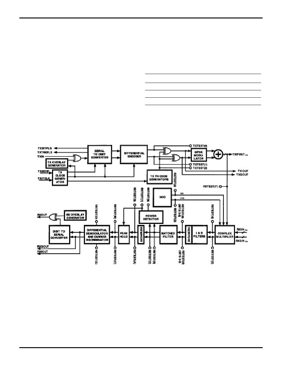
Z87200
Zilog
Spread-Spectrum Transceiver
4-27
4
All signals available at this port, with one exception, are ex-
pressed as two's complement values, ranging from ≠128
to +127 (80
H
to 7F
H
). The PN Matched Filter power output
values, available when the value in bits 3-0 of address 38
H
is set to either 1
H
or 8
H
, is an unsigned binary number,
ranging from 0 to 255 (0
H
to FF
H
).
The reset sequence that occurs when the receiver is dis-
abled will also reset the contents of address 38
H
to a value
of 0. If the RXTEST
7-0
bus is to be used to observe any
function other than the PN Matched Filter I and Q inputs,
then the appropriate value must be rewritten.
TXTEST (Pin 59)
Transmitter Test Output. TXTEST provides access to 3
test points within the transmitter as shown in The pin out-
put is selected according to the state of the two least sig-
nificant bits of the address line, ADDR
1-0
and the assign-
ments shown in Table 5. Note that this method of
accessing the transmitter test points is completely different
than the method by which the receiver test points are ac-
cessed. The state of the other address lines does not af-
fect this function, and this function is always enabled. The
availability of TXTEST output signals is only supported for
TXIFCLK speeds less than 20 MHz; output with clock
speeds greater than 20 MHz will be indeterminate.
Table 5. Transmitter Test Functions
ADDR
1-0
TXTEST
Description
0
H
ISM
Unspread I Symbol
1
H
QSYM
Unspread Q Symbol
2
H
SCODE
Spreading Code
Figure 10. Transmitter and Receiver Test Points
PS010202-0601

Z87200
Spread-Spectrum Transceiver
Zilog
4-28
CONTROL REGISTERS
Setting the Control Registers
The majority of the Z87200 control registers are complete-
ly independent and can be set or modified in any order.
Two exceptions, however, exist:
s
First, any time that the NCO is disabled, either through
use of pin MNCOEN or bit 0 of address 37
H
, the
frequency control word must be reloaded, either through
use of pin MFLD or bit 0 of address 00
H
, once the NCO
is re-enabled.
s
Second, setting bit 2 of address 37
H
to zero to disable
the receiver will also cause the data in address 38
H
to be
set to zero, thereby possibly changing the receiver test
point(s) that will be observed on the RXTEST pins.
Address 38
H
must be loaded with its desired value after
bit 2 of address 37
H
is again set to 1.
Downconverter Registers
Address 00
H
:
Bit 0 -- Frequency Control Word Load
This bit is used to load a frequency control value into the
NCO, thereby changing its output frequency. The signal is
internally synchronized to RXIFCLK to avoid intrinsic race
or hazard timing conditions.
The loading of the NCO may be performed by various
means. Setting this bit provides a synchronized internal
means to control update of the NCO. Alternatively, the
MFLD pin or the Z87200's programmable loop filter timing
circuitry may be used.
The MFLD input and bit 0 of address 00
H
are logically
ORed together so that, when either one is held low, a rising
edge on the other triggers the frequency load function
manually. The rising edge of this bit is synchronized inter-
nally so that, on the following sixth rising edge of RXIF-
CLK, the frequency control word is completely registered
into the NCO accumulator. The frequency load command
must not be repeated until after a delay of six RXIFCLK cy-
cles.
Address 01
H
:
Bit 0 -- Manual Sample Clock Enable
This bit selects the source of the internal baseband sam-
pling clock, which should be at twice the nominal PN chip
rate. The clock reference may be either supplied externally
by RXMSMPL or generated internally from RXIFCLK.
When this bit is set high, the baseband sampling rate of the
receiver is controlled by the external RXMSMPL signal.
When it is set low, the sampling clock is generated inter-
nally (at a rate determined by the Sample Rate Control
counter and set by bits 5-0 of address 02
H
) and the
RXMSMPL input is ignored.
Bit 1 -- Invert Loop Filter Value
This bit allows the sign of the output signal from the loop
filter to be inverted, thereby negating the value of the sig-
nal. The capability to invert the loop filter value permits the
carrier frequency error component generated in the de-
modulator to be either added to or subtracted from the Fre-
quency Control Word of the NCO. The correct setting will
depend on several factors, including whether high-side or
low-side downconversion is used.
When this bit is set low, the loop filter output is negated be-
fore being summed with the Frequency Control Word of
the NCO and is thus subtracted from the FCW; when this
bit is set high, the loop filter output is not negated and is
added to the FCW.
Bit 2 -- NCO Accumulator Carry In
This bit is primarily used as an internal test function and
should be set low for normal operation. When this bit is set
high, 1 LSB is added to the NCO accumulator each clock
cycle. When it is set low, the NCO accumulator is not af-
fected.
Bit 3 -- Two's Complement Input
The RXIIN
7-0
and RXQIN
7-0
input signals can be in either
two's complement or offset binary formats. Since all inter-
nal processing in the device operates with two's comple-
ment format signals, it is necessary to convert the RXIIN
7-
0
and RXQIN
7-0
inputs in offset binary format to two's com-
plement format by inverting the MSBs.
When this bit is set high, the device expects two's comple-
ment format inputs on RXIIN
7-0
and RXQIN
7-0
. When it is
set low, the device expects offset binary format on RXIIN
7-
0
and RXQIN
7-0
. In two's complement format, the 8-bit in-
put values range from ≠128 to +127 (80
H
to 7F
H
); in offset
binary format, the values range from 0 to +255 (00
H
to
FF
H
).
PS010202-0601

Z87200
Zilog
Spread-Spectrum Transceiver
4-29
4
Bits 7-4 -- Integrate and Dump Filter Viewport Control
The Z87200 incorporates viewport (data selector) circuitry
to select any three consecutive bits from the 14-bit output
of the Integrate and Dump (I & D) Filters in the Downcon-
verter block as the 3-bit inputs to the dual-channel PN
Matched Filter. The signal levels of the Integrate and
Dump Filter I and Q outputs reflect the input signal levels
and the number of samples integrated before the filter con-
tents are "dumped," where the number of samples is deter-
mined by the baseband sampling rate (nominally, twice the
PN chip rate) and the I.F. sampling rate (RXIFCLK). Set-
ting the viewport thus effectively normalizes the I & D Filter
outputs before further processing. The unsigned value, n,
of bits 7-4 of address 01
H
determines the 3-bit inputs to the
PN Matched Filter as the14-bit I & D Filter outputs divided
by 2
n
. Equivalently, bits 7-4 control the viewport of the In-
tegrate and Dump Filter outputs as shown in Note that
viewport control affects both I and Q channels of the Inte-
grate and Dump Filters.
Saturation protection is implemented for those cases when
the Integrate and Dump Filter output signal level overflows
the scaled range selected for the PN Matched Filter. When
the scaled value range is exceeded, the saturation protec-
tion limits the output word to the maximum or minimum val-
ue of the range according to whether the positive or nega-
tive boundary was exceeded.
Address 02
H
:
Bits 5-0 -- Receiver Baseband Sampling (Dump) Rate
Control
The baseband sampling rate should be set to twice the
nominal PN chip rate of the received signal and must be
less than or equal to half the rate of RXIFCLK. When bit 0
of address 01
H
is set low, the baseband sampling clock for
the Integrate and Dump Filter and all subsequent receiver
circuitry is referenced to RXIFCLK and generated internal-
ly. The receiver baseband sampling rate is then set to the
frequency of RXIFCLK/(n+1), where n is the value stored
in bits 5-0 and must range from 1 to 63. This feature is use-
ful in cases where a specific sample rate is required that is
an integer sub-multiple of f
RXIFCLK
. In cases where a sam-
ple rate is required that is not an integer sub-multiple of
f
RXIFCLK
, an external baseband sampling rate can be pro-
vided by the RXMSMPL input.
Addresses 03
H
through 06
H
:
NCO Frequency Control Word
The Z87200's internal NCO is driven by a frequency con-
trol word that is the sum of the frequency discriminator er-
ror value (generated in the demodulator) and the 32-bit fre-
quency control word (FCW) stored in this location. The four
8-bit registers at addresses 03
H
to 06
H
are used to store
the 32-bit frequency control word as shown in The LSB of
each byte is stored in bit 0 of each register.
The NCO frequency is then set by the FCW according to
the following formula:
In order to avoid in-band aliasing, f
NCO
must not exceed
50% of f
RXIFCLK
; normally, the FCW should be set so that
f
NCO
does not exceed ~35% of f
RXIFCLK
. While this limita-
tion may seem to restrict use of the NCO, higher I.F. trans-
mit or receive frequencies can generally be achieved by
using aliases resulting from digital sampling. The signal
bandwidth with respect to f
RXIFCLK
, the modulation type,
and the use of Direct I.F. or Quadrature Sampling Mode
also restrict the choice of NCO frequency, Theory of Oper-
ation.
PN Matched Filter Registers
Despreading of the received signal is accomplished in the
Z87200 with a dual (I and Q channel) PN Matched Filter.
Furthermore, the Z87200 is designed for burst signal oper-
ation, where each data burst begins with an Acquisi-
tion/Preamble symbol and is then followed by the actual in-
formation data symbols. Two separate and independent
PN codes can be employed, one for the Acquisition/Pre-
amble symbol, the other for the information symbols. Ac-
cordingly, the PN Matched Filter is supported by two PN
code registers to independently allow the programming of
two distinct codes up to 64 chips in length. The PN codes
are represented as a sequence of ternary-valued tap coef-
Table 6. Integrate & Dump Filter Viewport Control
Bits 7-4
I & D Bits Output to Matched Filter
0
H
2-0
1
H
3-1
2
H
4-2
3
H
5-3
∑ ∑ ∑
∑ ∑ ∑
∑ ∑ ∑
∑ ∑ ∑
A
H
12-10
B
H
13-11
Table 7. Integrate & Dump Filter Viewport Control
ADDR06H
ADDR 05H
ADDR04H
ADDR03H
Bits 31-24
Bits 23-16
Bits 15-8
Bits 7-0
f
RXIFCLK
x FCW
2
32
f
NCO
= __________
PS010202-0601

Z87200
Spread-Spectrum Transceiver
Zilog
4-30
CONTROL REGISTERS (Continued)
ficients, each requiring 2 bits of storage according to the
mapping shown in Table 8.
As a convention, Tap 0 is the first tap as the received sig-
nal enters the PN Matched Filter, and Tap 63 is the last. All
active taps of the PN Matched Filter, from Tap 0 up to Tap
(N-1), where N is the length of the PN code, should be pro-
grammed with tap coefficient values of +1 or -1 according
to the PN code sequence. Setting the end coefficients of
the PN Matched Filter registers to zero values permits the
effective length of the filter to be made shorter than 64
taps.
Addresses 07
H
through 16
H
:
Matched Filter Acquisition/Preamble Symbol
Coefficients
Addresses 07
H
to 16
H
contain the 64 2-bit Acquisition/Pre-
amble PN code coefficient values. The 128 bits of informa-
tion are stored in 16 8-bit registers at addresses 07
H
to 16
H
as shown in Table 8.
Addresses 17
H
through 26
H
:
Matched Filter Data Symbol Coefficients
Addresses 17
H
to 26
H
contain the 64 2-bit Data Symbol
PN code coefficient values. The 128 bits of information are
stored in 16 8-bit registers at addresses 17
H
to 26
H
as
shown in The contents of addresses 17
H
to 26
H
are inde-
pendent of and not affected by the contents of addresses
07
H
to 16
H
.
Address 27
H
:
Bit 0 -- Front End Processor Disable
The Front End Processor (FEP) averages the two base-
band samples per chip by adding consecutive pairs of
samples. The function may be disabled for test purposes
by using this bit: when set low, the FEP is enabled and in
its normal mode of operation; when set high, the FEP is
disabled.
Power Estimator Registers
Address 28
H
:
Bits 1-0 -- Matched Filter Viewport Control
The Z87200 incorporates viewport (data selector) circuitry
to select any eight consecutive bits from the 10-bit outputs
of the PN Matched Filter as the 8-bit inputs to the Power
Estimator and DPSK Demodulator blocks. The Symbol
Tracking Processor, however, operates on the full 10-bit
PN Matched Filter outputs before the viewport is applied.
The signal levels of the PN Matched Filter output reflect
the number of chips per symbol and the signal-to-noise ra-
tio of the signal. Setting the viewport thus effectively nor-
malizes the PN Matched Filter outputs prior to further pro-
cessing. The unsigned value, n, of bits 1-0 of address 28
H
determines the 8-bit input to the Power Estimator and
DPSK Demodulator blocks as the 10-bit PN Matched Filter
output divided by 2
n
. Equivalently, bits 1-0 control the
viewport of the PN Matched Filter output as shown in Note
Table 8. PN Matched Filter Tap Values
Tap Bits 1,0
Tap Coeff
X
0
0
0
1
+1
1
1
-1
Table 9. Acquisition/Preamble Coefficient Storage
Address 16
H
Bits 7,6
Bits 5,4
Bits 3,2
Bits 1,0
Coeff. 63
Coeff. 62
Coeff. 61
Coeff. 60
Address 15
H
Bits 7,6
Bits 5,4
Bits 3,2
Bits 1,0
Coeff. 59
Coeff. 58
Coeff. 57
Coeff. 56
- - -
- - -
- - -
- - -
- - -
- - -
- - -
- - -
Address 08
H
Bits 7,6
Bits 5,4
Bits 3,2
Bits 1,0
Coeff. 7
Coeff. 6
Coeff. 5
Coeff. 4
Address 07
H
Bits 7,6
Bits 5,4
Bits 3,2
Bits 1,0
Coeff. 3
Coeff. 2
Coeff. 1
Coeff. 0
Table 10. Data Symbol Coefficient Storage
Address 26
H
Bits 7,6
Bits 5,4
Bits 3,2
Bits 1,0
Coeff. 63
Coeff. 62
Coeff. 61
Coeff. 60
Address 25
H
Bits 7,6
Bits 5,4
Bits 3,2
Bits 1,0
Coeff. 59
Coeff. 58
Coeff. 57
Coeff. 56
- - -
- - -
- - -
- - -
- - -
- - -
- - -
- - -
Address 18
H
Bits 7,6
Bits 5,4
Bits 3,2
Bits 1,0
Coeff. 7
Coeff. 6
Coeff. 5
Coeff. 4
Address 17
H
Bits 7,6
Bits 5,4
Bits 3,2
Bits 1,0
Coeff. 3
Coeff. 2
Coeff. 1
Coeff. 0
PS010202-0601

Z87200
Zilog
Spread-Spectrum Transceiver
4-31
4
that viewport control affects both I and Q channels of the
PN Matched Filter output.
Saturation protection is implemented for those cases when
the PN Matched Filter output signal level overflows the
scaled range selected for the Power Estimator and DPSK
Demodulator. When the scaled value range is exceeded,
the saturation protection limits the output word to the max-
imum or minimum value of the range according to whether
the positive or negative boundary was exceeded.
Acquisition and Tracking Processor
Registers
The Acquisition and Tracking Processor Registers allow
the user to configure how the PN Matched Filter outputs for
the Acquisition/Preamble symbol and the data symbols
that follow thereafter are treated in the Symbol Tracking
Processor. Since operation of the Z87200 receiver pre-
sumes symbol-synchronous PN modulation, processing of
the PN Matched Filter outputs can be used for symbol syn-
chronization prior to DPSK demodulation. The Acquisi-
tion/Preamble symbol and the data symbols may have dif-
ferent PN spreading codes, however, and so the PN
Matched Filter outputs may exhibit different signal levels
due to the different code lengths and auto-correlation
properties. The control registers in this block allow such
differences to be treated, as well as permitting specifica-
tion of the number of receive data symbols per burst and
other parameters associated with burst data communica-
tions.
The I and Q channel outputs of the PN Matched Filter are
processed to estimate the correlation signal power at each
baseband sampling instant. This estimated signal power is
compared with the contents of the Acquisition/Preamble
and Data Symbol Threshold registers, as appropriate, to
determine whether "successful" correlation has been de-
tected. Successful detection in acquisition mode immedi-
ately switches the receiver to despread and track the ex-
pected subsequent data symbols, while successful
detection thereafter yields symbol synchronization. The
threshold register values must be set by the user to satis-
factorily detect the correlation peak in noise obtained when
the received PN-spread signal is correlated against a local
version of the PN code by the PN Matched Filter. Once the
power estimation value exceeds the threshold register val-
ue, a successful correlation is assumed to have been de-
tected. Further operations in the Symbol Tracking Proces-
sor then handle the possibility of multiple detects per
symbol, missed detects, etc.
The choice of the threshold values will be determined by
several factors. Arithmetically, the digital baseband sam-
ples of the received signal are multiplied by the PN
Matched Filter tap coefficients each baseband sample
clock cycle and the results are summed to provide a corre-
lation value. The I and Q PN Matched Filter correlated out-
put values are then used to estimate the signal power ac-
cording to the following approximation:
Max{Abs(I),Abs(Q)}+1/2 Min{Abs(I), Abs(Q)}.
The magnitude of the estimated power thus depends on
several variables, including the setting of the Integrate and
Dump Filter viewport, the PN code length and autocorrela-
tion properties, and the magnitudes of the incoming
RXIIN
7-0
and RXQIN
7-0
signals. The actual threshold val-
ues that should be programmed will therefore vary from
application to application.
Addresses 29
H
and 2A
H
:
Acquisition/Preamble Threshold
Addresses 29
H
and 2A
H
contain the unsigned Acquisi-
tion/Preamble Threshold value, as shown in This value is
used for comparison with the estimated signal power from
the PN Matched Filter to determine whether a successful
correlation has been detected in acquisition mode. The
Acquisition/Preamble Threshold value must be set by the
user to satisfactorily detect the correlation peak in noise
obtained when the received PN-spread Acquisition/Pre-
amble is correlated against a local version of the Acquisi-
tion/Preamble PN code by the PN Matched Filter. Once
the power estimation value exceeds the threshold value, a
successful correlation is assumed to have been detected.
Note that the Symbol Tracking Processor does not insert
missed detect pulses when the device is in acquisition
mode.
Addresses 2B
H
and 2C
H
:
Data Symbol Threshold
Addresses 2B
H
and 2C
H
contain the Data Symbol Thresh-
old value, as shown in This value is used for comparison
with the estimated signal power from the PN Matched Fil-
ter to determine whether a successful correlation has been
detected for each data symbol. The Data Symbol Thresh-
old value must be set by the user to satisfactorily detect the
correlation peak in noise obtained when the received PN-
spread data symbol is correlated against a local version of
the data symbol PN code by the PN Matched Filter. Once
the power estimation value exceeds the threshold value, a
successful correlation is assumed to have been detected.
If bit 2 of address 30
H
is set low, then the Symbol Acquisi-
Table 11. Matched Filter Viewport Control
Bits 1-0
ISUM, QSUM
0
0
Bits 7-0
0
1
Bits 8-1
1
X
Bits 9-2
Table 12. Acquisition/Preamble Threshold Storage
ADDR 2A
H
ADDR 29
H
Bits 1-0
Bits 7-0
Acq. Thresh. Bits 9-8
Acq. Thresh. Bits 7-0
PS010202-0601

Z87200
Spread-Spectrum Transceiver
Zilog
4-32
CONTROL REGISTERS (Continued)
tion Processor will insert a detect pulse at the appropriate
time if a successful correlation is not detected as expected
a priori.
Address 2D
H
:
Bits 5-0 -- Rx Chips per Data Symbol
The number of PN chips per data symbol in the receiver is
controlled by address 2D
H
. The unsigned value must
range from 1 to 63 (01
H
to 3F
H
), where the number of chips
per data symbol will be this value plus 1. The
a priori num-
ber of PN chips per data symbol, where this value must be
equal to the number of non-zero coefficients stored in the
Data Symbol Coefficient Registers (addresses 17
H
to 26
H
)
for the PN Matched Filter, is used to help control symbol
timing in the receiver. Since acquisition is purely based on
correlation of a single received Acquisition/Preamble sym-
bol, the corresponding number of chips per Acquisi-
tion/Preamble symbol is not required and no similar regis-
ter is provided for such use.
Address 2E
H
:
Receiver Data Symbols per Burst (bits 7-0)
The data stored as two bytes in addresses 2E
H
(LS Byte)
and 3A
H
(MS Byte) define the number of data symbols per
burst. This unsigned value must range from 3 to 65,535
(0003
H
to FFFF
H
), and the number of data symbols per
burst will be this value minus 2, giving a range of 1 to
65,533. Note that the range is slightly different from that
supported by the Z87200's transmitter. Once the number
of received data symbols processed exceeds this number,
the burst is assumed to have ended and the receiver im-
mediately returns to acquisition mode, ready for the next
burst.
Address 2F
H
:
Missed Detects per Burst Threshold
To monitor the reception quality of the received burst data
symbols, the Z87200 incorporates a feature within its
tracking algorithm that tallies the number of received data
symbols whose PN Matched Filter correlation output did
not exceed the Data Symbol Threshold value.
Whenever a "missed detect" occurs, the tracking algorithm
will generate and insert a detect signal at the sample clock
cycle corresponding to the expected correlation peak in or-
der to maintain a continuous train of data symbols and
symbol clocks. Simultaneously, a "missed detect" pulse
will be generated internally and tallied for the current burst.
When the accumulated number of missed detects is great-
er than the value stored in address 2F
H
, the device will ter-
minate reception of the current burst and return to acquisi-
tion mode to await the next burst.
The unsigned value in address 2F
H
must range from 1 to
255 (01
H
to FF
H
), where this value is the maximum num-
ber of missed detects per burst allowed before the burst
terminates. This function can be disabled by setting bit 5 of
address 30
H
high.
Address 30
H
:
Bit 0 -- Manual Detect Enable
While the receiver is in acquisition mode, valid bursts may
be ignored by setting this bit high. When it is set low (nor-
mal operation), the detection of a burst's Acquisition/Pre-
amble symbol is enabled. Setting this bit high allows the
user to force the device to ignore Acquisition/Preamble
symbols that would normally be successfully acquired.
This feature could be used, for example, in a system em-
ploying multiple receivers with identical PN codes in a
Time Division Multiple Access scheme where time-syn-
chronized device management could be supported
through dynamic setting of this bit.
Acquisition and Tracking Processor
Registers
Bit 1 -- Manual Punctual
This bit enables the user to completely disable the internal
tracking circuitry and force symbol information to be trans-
ferred to the demodulator punctually at the symbol rate de-
termined by the number of chips per data symbol informa-
tion programmed into address 2D
H
. This function
overrides the symbol tracking algorithm, although the ab-
sence of a successful correlation will continue to be tallied
as a missed detect and compared against the value stored
in address 2F
H
to monitor signal quality unless disabled by
bit 5 of address 30
H
. When bit 1 is set low, the Z87200 will
operate in its normal mode with symbol timing derived from
the symbol tracking processor; when set high, symbol tim-
ing is derived from the
a priori number of chips per data
symbol stored in bits 5-0 of address 2D
H
.
Bit 2 -- Force Continuous Acquisition
This bit enables the user to force the receiver to remain in
acquisition mode even after successful detection of the
Acquisition/Preamble symbol. When so commanded, the
receiver will continuously process only Acquisition/Pream-
ble symbols and will not switch from acquisition mode. This
function may be used under manual control to receive a
series of repeated Acquisition/Preamble symbols in order
to increase the confidence level of burst detection before
beginning demodulation of the data symbol information.
When this bit is set high, the device will be locked in acqui-
sition mode and the Symbol Tracking Processor will not in-
Table 13. Data Symbol Threshold Storage
ADDR 2C
H
ADDR 2B
H
Bits 1-0
Bits 7-0
Data Thresh. Bits 9-8
Data Thresh. Bid 7-0
PS010202-0601

Z87200
Zilog
Spread-Spectrum Transceiver
4-33
4
sert missed detect pulses; when set low, normal operation
will be enabled whereby data symbols are automatically
processed immediately following detection of an Acquisi-
tion/Preamble symbol.
Bit 3 -- Bypass Max. Power Selector
The Z87200's receiver acquisition and tracking circuitry in-
cludes a function that continuously selects the highest es-
timated power level out of the three most recent consecu-
tive estimated power levels from the PN Matched Filter. As
the contents of the sliding 3-sample window change each
cycle of the baseband sampling clock, a new determina-
tion of the highest power level is made from the current set
of the three most recent power level values. The correlated
I and Q channel values within the 3-sample window corre-
sponding in time to the highest observed power level are
then available to be processed in the demodulator.
This function assures that, within any 3-sample period, the
I and Q channel values corresponding to the highest esti-
mated power level will be selected over the two other pairs
of correlated values even if the estimated power levels of
the other pairs exceed the programmed threshold. The
Maximum Power Selector is used in normal operation of
the Z87200 so that the tracking algorithm discriminates by
estimated power levels rather than exact timing intervals,
thereby allowing the receiver to adjust to dynamic changes
of the symbol phase. In cases where specific correlation
values are desired regardless of their associated power
level, bit 3 of address 30
H
enables the 3-sample power dis-
criminator to be bypassed, thereby making the outputs of
the PN Matched Filter available directly to the demodula-
tor.
When this bit is set high, the Maximum Power Selector is
bypassed; when it is set low, the Selector is enabled,
where this is the normal operating mode.
Bit 4 -- Half Symbol Pulse Off
The Z87200 generates two bit clock pulses per symbol
when operating in QPSK mode, one at the mid-point of
each symbol and one at the end of each symbol. These
clocks are used by the Output Processor to manage data
flow.
When this bit is set high, the mid-point pulse is sup-
pressed; when it is set low, the device operates in its nor-
mal mode. This function is primarily used for test purposes
and should not normally be used.
Bit 5 -- Missed Detects Per Burst Off
To monitor the quality of the received burst data symbols,
the Symbol Tracking Processor keeps track of the cumu-
lative number of received data symbols per burst whose
estimated correlation power level did not exceed the spec-
ified Data Symbol Threshold value. When the accumulat-
ed number of missed detects equals the Missed Detects
per Burst Threshold value stored in address 2F
H
, the de-
vice will terminate the reception of the current burst with
the next missed detect and return to acquisition mode to
await the next burst.
When bit 5 is set low, the "missed detect" function operates
normally; when set high, this function is disabled, allowing
the device to be operated until the end of the specified data
burst even when the number of "missed detects" exceeds
the Missed Detects per Burst Threshold.
Bit 6 -- Receiver Symbols Per Burst Off
The data stored in addresses 2E
H
and 3A
H
defines the
number of data symbols per burst that will be processed by
the receiver. This unsigned value must range from 3 to
65,535 (0003
H
to FFFF
H
), and the number of data symbols
per burst will be this value minus 2. Once the number of
data symbols processed by the receiver exceeds this num-
ber, the burst is assumed to have ended and the receiver
will immediately return to acquisition mode.
When bit 6 is set high, the function is disabled, providing
an option to track data symbols under external control for
bursts of more than 65,533 data symbols or indefinitely for
continuous transmission; when set low, the function will
operate normally as defined by the value stored in ad-
dresses 2E
H
and 3A
H
.
Address 31
H
:
Bit 0 -- Manual Detect Pulse
This bit provides the user a means to externally generate
symbol timing, bypassing and overriding the internal sym-
bol power estimation and tracking circuitry. This function
may be useful in applications where the dynamic charac-
teristics of the transmission environment require unusual
adjustments to the symbol timing.
When bit 0 of address 30
H
is set high (Manual Detect En-
able) and when RXMDET is low, a rising edge on this bit
will generate a detect pulse. The function can also be per-
formed by means of the RXMDET input signal. Bit 0 of ad-
dress 31
H
and the RXMDET input are logically ORed to-
gether so that, when either one is held low, a rising edge
on the other triggers the manual detect function. The rising
edge of this bit is synchronized internally so that on the
second rising edge of the baseband sampling clock that
follows, the rising edge of bit 0 will transfer the I and Q
channel correlated output values of the PN Matched Filter
to the DPSK Demodulator.
Address 32
H
:
Bit 0 -- Receiver Manual Abort
This bit enables the user to manually force the Z87200 to
cease reception of the present burst of data symbols and
prepare for acquisition of a new burst. This function can be
used to reset the receiver and prepare to receive a priority
transmission signal under precise timing control, giving the
user the ability to control the current state of the receiver
as needed.
PS010202-0601

Z87200
Spread-Spectrum Transceiver
Zilog
4-34
CONTROL REGISTERS (Continued)
When RXMABRT is set low, a rising edge on bit 0 of ad-
dress 32
H
will execute the abort function. The function can
also be performed by means of the RXMABRT input. The
RXMABRT input and bit 0 of address 32
H
are logically
ORed together so that, when either one is held low, a rising
edge on the other triggers the abort function. The second
rising edge of the internal baseband sampling clock that
follows a rising edge of this bit will execute the abort and
also clear the symbols-per-burst, samples-per-symbol,
and missed-detects-per-burst counters. The counters will
be reactivated on the detection of the next Acquisition/Pre-
amble symbol or by a manual detect signal.
Demodulator Registers
Address 33
H
:
Bits 1-0 -- Signal Rotation Control
These bits control the function of the Signal Rotation Block
used in demodulation of the differentially encoded BPSK,
QPSK, or
/4 QPSK signals. The previous symbol will be
rotated in phase with respect to the current symbol as
shown in Table 14, where I
OUT
and Q
OUT
are the I and Q
channel outputs of the Signal Rotation Block and I
IN
and
Q
IN
are the inputs. The normal settings are 0 X (no rota-
tion) for BPSK and
/4 QPSK signals and 1 1 (≠45
∞
rota-
tion) for conventional QPSK signals.
Bit 2 -- Not Used
Bit 2 of address 33
H
is not used and must always be set
low (0).
Bit 3 -- Loop Clear Disable
The setting of this bit determines whether the Loop Filter's
K2 accumulator is reset or not when the Z87200 receiver
function is turned off when the input signal MRXEN is set
low.
When bit 3 is set low, the Loop Filter's K2 accumulator will
be reset to zero whenever MRXEN is set low to disable the
receiver function. When bit 3 is set high, this function is dis-
abled and the contents of the accumulator are not affected
when MRXEN transitions from high to low. The optimum
setting of this bit will depend on the stability of the oscilla-
tors used for carrier generation and frequency translation
in the system and the length of the period between bursts.
If the oscillators are stable and the period between bursts
is not very long, the optimum setting of this bit will be low
so that at the start of each burst the tracking loop will re-
sume from its state at the end of the previous burst. If the
oscillators are not stable or if the period between bursts is
long with respect to the oscillators' stability, then the opti-
mum setting may be high so that the tracking loop will re-
start from its initial state at the start of each burst.
Bits 7-4 -- AFC Viewport Control
The Z87200 incorporates viewport (data selector) circuitry
to select any eight consecutive bits from the 17-bit output
of the Frequency Discriminator as the 8-bit input to the
Loop Filter block to implement the Z87200's AFC function.
The unsigned value, n, of bits 7-4 of address 33
H
deter-
mines the 8-bit input to the Loop Filter as the 17-bit Fre-
quency Discriminator output divided by 2
n
. Equivalently,
bits 7-4 control the viewport of the Frequency Discrimina-
tor output as shown in Table 14.
Table 14. Signal Rotation Control
Bits 1,0
I
OUT
Q
OUT
Resulting
Rotation
0, X
I
IN
Q
IN
No rotation
1,0
I
IN
-Q
IN
Q
IN
+I
IN
+45
∞
rotation
1,1
I
IN
+ Q
IN
Q
IN
-I
IN
-45
∞
rotation
Table 15. AFC Viewport Control
Bits 7-4
Discrim. bits output to Loop Filter
0
H
7-0
1
H
8-1
2
H
9-2
3
H
10-3
∑ ∑ ∑
∑ ∑ ∑
∑ ∑ ∑
∑ ∑ ∑
8
H
15-8
9
H
16-9
A
H
-F
H
Not used
PS010202-0601

Z87200
Zilog
Spread-Spectrum Transceiver
4-35
4
Saturation protection is implemented for those cases when
the Frequency Discriminator output signal level overflows
the scaled range selected for the Loop Filter. When the
scaled value range is exceeded, the saturation protection
limits the output word to the maximum or minimum value
of the range according to whether the positive or negative
boundary was exceeded.
Address 34
H
:
Bits 4-0 -- K2 Gain Value
Bits 4-0 control the gain factor K2 within the Loop Filter.
The gain factor multiplies the signal before the K2 accumu-
lator by a value of 2
n
, where n is the 5-bit K2 Gain Value.
The value must range from 0 to 21 (15
H
) as shown in Table
15.
Bit 5 -- K2 On
This bit enables or disables the K2 path of the Loop Filter.
Setting this bit low resets the K2 accumulator and keeps it
reset; setting this bit high enables the path and turns on
K2.
Bit 6 -- Carry In One Half
When this bit is set high, the value of 1/2 of an LSB is add-
ed to the accumulator of the K2 path of the Loop Filter
each symbol period. This function can be useful in cases
where the scale and gain functions that precede the accu-
mulator produce quantized values with significant error. In
such cases, the processing of two's complement numbers
by the accumulator will compound the error over time.
Since truncation of two's complement numbers leads to a
negative bias of 1/2 of an LSB when the error is random,
adding 1/2 of an LSB per symbol can compensate by av-
eraging the error to zero.
When bit 6 of address 34
H
is set high, a value of 1/2 will be
added to the accumulator input each symbol cycle; when
it is low, a zero will be added.
Address 35
H
:
Bits 4-0 -- K1 Gain Value
Bits 4-0 control the gain factor K1 within the Loop Filter.
The gain factor multiplies the signal by a value of 2
n
, where
n is the 5-bit K1 Gain Value. The value must range from 0
to 21 (15
H
), as shown in Table 16.
Bit 5 -- K1 On
This bit enables or disables the K1 path of the Loop Filter.
Setting this bit low disables the K1 path; setting this bit high
enables the path and turns on K1.
Bit 6 -- Freeze Loop
This bit enables the Loop Filter to be held constant during
symbol cycles, thereby fixing the output frequency of the
NCO at the value established by the Loop Filter when bit 6
was set high. This function can be useful in cases where a
carrier offset has been tracked by the Loop Filter and ad-
ditional Doppler offsets are to be ignored.
When this bit is set high, it freezes the output of the Loop
Filter; when it is set low, the Loop Filter is enabled and pro-
cesses the frequency error information in the usual way.
Table 16. K2 Gain Values
Bits 4-0
Gain in K2 Path
00
H
2
0
01
H
2
1
∑ ∑ ∑
∑ ∑ ∑
∑ ∑ ∑
∑ ∑ ∑
14
H
2
20
15
H
2
21
Table 17. K1 Gain Values
Bits 4-0
Gain in K1 Path
00
H
20
01
H
21
∑∑∑∑∑
∑∑∑∑∑
∑∑∑∑∑
∑∑∑∑∑
14
H
2
20
15
H
2
21
PS010202-0601

Z87200
Spread-Spectrum Transceiver
Zilog
4-36
CONTROL REGISTERS (Continued)
Output Processor Control Registers
Address 36
H
:
Bit 0 -- Reverse I and Q
In QPSK mode, the order in which the received I and Q bit
information is output may be reversed by setting this bit
high. This function has the effect of interchanging I and Q
channels. Normally, when this bit is set low, the I-channel
bit will precede the Q-channel bit in each symbol period.
When bit 0 is set high, the Q-channel bit will precede the I-
channel bit each symbol period.
Bit 1 -- BPSK Enable
This bit configures the Output Processor to output either
one bit per symbol (BPSK mode) or two bits per symbol
(QPSK mode). In addition, it enables the user to output the
I-channel information only or the Q-channel information
only, depending on the value of bit 0. Table 18 shows the
configuration of the output processor for all combinations
of the values of bits 0 and 1.
Bit 1 also sets the Frequency Discriminator into either
BPSK or QPSK mode. The Z87200 receiver uses Dot and
Cross product results generated within the DPSK Demod-
ulator to develop the error signal used to form a closed-
loop AFC for carrier frequency acquisition and tracking.
When bit 1 is set high, the discriminator circuitry is in BPSK
mode and the Frequency Discriminator function is calcu-
lated as:
Cross
16-0
x Dot
MSB
.
When bit 1 is set low, the discriminator circuitry is in QPSK
mode and the Frequency Discriminator function is calcu-
lated as:
(Cross
16-0
x Dot
MSB
) ≠ (Dot
16-0
x Cross
MSB
).
Bit 2 ≠ Invert Output
This bit inverts the output bits of both the I and Q Chan-
nels. The inversion will occur at the output pins RXOUT,
RXIOUT, and RXQOUT.
When this bit is set low, the outputs are not inverted; when
it is set high, the outputs are inverted.
Output Processor Control Registers
Address 37
H
:
Bit 0 -- NCO Enable
The function of this bit is to allow the power consumed by
the operation of the NCO circuitry to be minimized when
the Z87200 is not receiving. The NCO can also be disabled
while the Z87200 is transmitting provided that the
Z87200's on-chip BPSK/QPSK modulator is not being
used. With the instantaneous acquisition properties of the
PN Matched Filter, it is often desirable to shut down the re-
ceiver circuitry to reduce power consumption, resuming re-
ception periodically until an Acquisition/Preamble symbol
is acquired. Setting bit 0 low holds the NCO in a reset
state; setting bit 0 high then reactivates the NCO, where it
is necessary to reload the frequency control word into the
NCO. Note that this bit operates independently of bits 1
(Transmitter Enable) and 2 (Receiver Enable), where
those bits have similar control over the transmit and re-
ceive circuitry, respectively.
Bit 0 of address 37
H
performs the same function as MN-
COEN, and these two signals are logically ORed together
to form the overall control function. When bit 0 is set low,
MNCOEN controls the activity of the NCO circuitry and,
when MNCOEN is set low, bit 0 controls the activity of the
NCO circuitry. When either bit 0 or MNCOEN (whichever
is in control, as defined above) goes low, a reset sequence
occurs on the following RXIFCLK cycle to virtually disable
all of the NCO circuitry, although the user programmable
control registers are not affected by the power down se-
quence. Upon reactivation (when either MNCOEN or bit 0
of address 37
H
return high), the NCO must be reloaded
with frequency control information either by means of the
MFLD input or by writing 01
H
into address 00
H
.
Bit 1 -- Transmitter Enable
A rising edge on this bit causes the transmit sequence to
begin so that the Z87200 first transmits a single Acquisi-
tion/Preamble symbol followed by data symbols. Bit 1 of
address 37
H
should be set low after the last symbol has
been transmitted to minimize power consumption of the
transmitter circuit. Bit 1 of address 37
H
operates indepen-
dently of bits 2 and 0, where those bits have similar control
over the receive and NCO circuitry, respectively.
Table 18. Output Processor Modes
Bit 1
Bit 0
Output Processor Mode
0
0
QPSK mode with I-Channel Bit
Preceding Q-Channel Bit
0
1
QPSK mode with Q-Channel Bit
Preceding I-Channel Bit
1
0
BPSK mode with I-Channel
Information Output
1
1
BPSK mode with Q-Channel
Information Output
PS010202-0601

Z87200
Zilog
Spread-Spectrum Transceiver
4-37
4
When input signal MTXEN is set low, bit 1 of address 37
H
controls the activity of the transmit circuitry and, when
MTXEN is set low, bit 1 controls this function. When either
bit 1 or MTXEN (whichever is in control, as defined above)
goes low, a reset sequence occurs on the following TXIF-
CLK cycle to virtually disable all of the transmitter data
path, although the user programmable control registers
are not affected by the power down sequence.
Bit 2 -- Receiver Enable
The function of this bit is to allow power consumed by the
operation of the receiver circuitry to be minimized when the
device is not receiving. With the instantaneous acquisition
properties of the PN Matched Filter, it is often desirable to
shut down the receiver circuitry to reduce power consump-
tion, resuming reception periodically until an Acquisi-
tion/Preamble symbol is acquired. Setting bit 2 low reduc-
es the power consumption substantially. When bit 2 is set
high, the receiver will automatically power up in acquisition
mode regardless of its prior state when it was powered
down. Bit 2 of address 37
H
operates independently of bits
1 and 0 of address 37
H
, where these signals have similar
control over the transmit and NCO circuitry, respectively.
Bit 2 of address 37
H
performs the same function as MRX-
EN, and these two signals are logically ORed together to
form the overall control function. When bit 2 of address 37
H
is set low, MRXEN controls the activity of the receiver cir-
cuitry and, when MRXEN is set low, bit 2 of address 37
H
controls the activity of the receiver circuitry. When either bit
2 or MRXEN (whichever is in control, as defined above)
goes low, a reset sequence begins on the following RXIF-
CLK cycle and continues through a total of six RXIFCLK
cycles to virtually disable all of the receiver data paths. The
user- programmable control registers are not affected by
the power down sequence, with the exception of
RXTEST
7-0
(address 38
H
), which is reset to 0. If the
RXTEST
7-0
bus is being used to read any function other
than the PN Matched Filter I and Q inputs, the value must
be rewritten.
Address 38
H
:
Bits 3-0 -- RXTEST
7-0
Function Select
The data stored in bits 3-0 of address 38
H
selects the sig-
nal available at the RXTEST
7-0
bus (pins 41-48). These
pins provide access to 16 test points within the receiver ac-
cording to the data stored in bits 3-0 of address 38
H
and
the assignments shown in The validity of the RXTEST
7-0
outputs at RXIFCLK speeds greater than 20 MHz is de-
pendent on the output selected: outputs that change more
rapidly than once per symbol may be indeterminate.
Note that the reset sequence that occurs when the receiv-
er is disabled will also reset the contents of address 38
H
to
a value of 0. If the RXTEST7-0 bus is to be used to observe
any function other than the PN Matched Filter I and Q in-
puts, then the appropriate value must be rewritten.
Address 39
H
:
Bits 6-0 -- Matched Filter Power Saver
The data stored in bits 6-0 of address 39
H
allows the un-
used sections of the PN Matched Filter to be turned off
when the PN Matched Filter is configured to be less than
64 taps long for data symbols. All taps are always fully
powered when the device is in acquisition mode.
The PN Matched Filter is split into seven 9-tap sections,
and the power to each section is controlled by the settings
of bits 6-0 of address 39
H
, as shown in Table 19.
Power control is not provided for Tap 0, the first tap of the
PN Matched Filter, since Tap 0 is always used no matter
what the PN code length. Setting a bit high in bits 6-0 of ad-
dress 39
H
turns off the power to the corresponding block
of taps of the PN Matched Filter. The power should only be
turned off to those blocks of taps for which all the tap coef-
ficients in that block have been set to zero
Address 3A
H
:
Receiver Data Symbols per Burst (bits 15-8)
The data stored as two bytes in addresses 2E
H
(LS byte)
and 3A
H
(MS byte) defines the number of data symbols per
burst. This unsigned value must range from 3 to 65,535
(0003
H
to FFFF
H
), and the number of data symbols per
burst will be this value minus 2, giving a range of 1 to
65,533. Note that the range is slightly different from that in
the transmitter. Once the number of received data symbols
processed exceeds this number, the burst is assumed to
have ended and the Z87200 immediately returns to acqui-
sition mode to await the next burst.
Table 19. Matched Filter Tap Power Control
Bit in Addr. 39
H
MF Taps Controlled
0
1-9
1
10-18
2
19-27
3
28-36
4
37-45
5
46-54
6
55-64
PS010202-0601

Z87200
Spread-Spectrum Transceiver
Zilog
4-38
CONTROL REGISTERS (Continued)
Address 3B
H
:
Bit 0 -- Matched Filter Loopback Enable
The Z87200 incorporates a loopback capability that feeds
the encoded and spread transmit signals TXIOUT and TX-
QOUT directly into the PN Matched Filter inputs. This test
mode allows the baseband portion of the system to be test-
ed independently of the BPSK/QPSK Modulator and
Downconverter.
Setting bit 0 of address 3B
H
high enables this loopback
path; setting it low puts the device into its normal operating
mode.
Bit 1 -- I.F. Loopback Enable
The Z87200 incorporates a loopback capability that feeds
the encoded, spread and modulated transmit signal
TXIFOUT
7-0
directly into the receiver RXIIN
7-0
input. This
test mode allows the entire digital portion of the system to
be tested. Since only the I channel is provided as an input,
I.F. loopback requires that the PN chip rate and RXIFCLK
rate be consistent with Direct I.F. Sampling Mode.
Setting bit 1 of address 3B
H
high enables this loopback
path; setting it low puts the device into its normal operating
mode.
Bits 3-2 -- Receiver Overlay Select
The Z87200 incorporates programmable overlay code
generators in both the transmitter and receiver. When en-
abled, the selected receiver overlay code is subtracted
from the data symbols, one overlay bit per symbol in both
BPSK and QPSK modes. No synchronization beyond the
burst acquisition synchronization that is intrinsic to opera-
tion of the Z87200 is required since the overlay code gen-
erators in both the transmitter and the receiver are auto-
matically reset at the start of each burst. The addition of
the overlay code randomizes the transmitted data se-
quence to guarantee that the spectrum of the transmitted
signal will be adequately whitened and will not contain a
small number of spectral lines even when the data itself is
not random.
Three transmit and receive overlay codes can be selected,
where they are each maximal length sequences with
lengths of 63, 511 and 1023 symbols. The receiver overlay
codes are enabled and selected by the settings of bits 3-2
of address 3B
H
, as shown in Table 19.
Addresses 3C
H
through 3F
H
: Unused
Transmit Control Registers
Address 40
H
:
Bit 0 -- Transmit BPSK
This bit configures the transmitter for either BPSK or
QPSK mode transmission. and differential encoding.
If programmed for BPSK mode, data is requested by the
Z87200 by a rising edge of output signal TXBITPLS, where
TKBITPLS is generated once per symbol, one chip period
before the end of the current symbol. At the end of the
symbol duration, the TXIN data is latched into the device.
TXBITPLS falls low immediately following the rising edge
of TXIFCLK, which latches the TXIN value, and is generat-
ed repeatedly at the symbol rate as long as the input signal
MTXEN remains high.
In QPSK mode, data is requested by the Z87200 by a ris-
ing edge of output signal TXBITPLS, where this signal is
generated in this mode twice per symbol, first one chip pe-
riod before the middle of the symbol and then one chip pe-
riod before the end of the symbol. TXBITPLS requests the
data exactly one chip cycle before latching the TXIN data
into the device. TXBITPLS falls low immediately following
the rising edge of TXIFCLK, which latches the TXIN value.
When bit 0 of address 40
H
is set low, the transmitter is con-
figured in QPSK mode; when it is set high, the transmitter
is configured in BPSK mode.
Table 20. Receiver Overlay Code Select
Bits 3-2 in
Addr. 3B
H
Overlay Code Length
and Polynomial
0
Overlay Code Disabled
1
63: 1 +x
-2
+x
-3
+x
-5
+x
-6
2
511: 1 +x
-2
+x
-3
+x
-5
+x
-9
3
1023: 1 + x
-2
+x
-3
+x
-5
+x
-10
PS010202-0601

Z87200
Zilog
Spread-Spectrum Transceiver
4-39
4
Bit 1 -- Offset Binary Output
The TXIFOUT
7-0
output signals can be in either two's com-
plement or offset binary formats. Since all internal pro-
cessing in the device uses two's complement format sig-
nals, the MSB of the two's complement modulated
transmitter output must be inverted if the output is to be in
offset binary format.
When this bit is set high, the TXIFOUT
7-0
output will be in
offset binary format and, when it is set low, the signal will
be in two's complement format. In two's complement for-
mat, the 8-bit output values range from ≠128 to +127 (80
H
to 7F
H
); in offset binary format, the values range from 0 to
+255 (00
H
to FF
H
).
Bit 2 -- Manual Chip Clock Enable
This bit enables the PN chip rate to be controlled by either
the internal chip rate clock generator or by the external in-
put signal TXMCHP. The TXMCHP input allows the user
to manually insert a single PN chip clock pulse or continu-
ous stream of pulses. This feature is useful in cases where
a specific chip rate is required that cannot be derived by
the internal clock generator which generates clocks of in-
teger sub-multiples of the frequency of TXIFCLK. The sig-
nal is internally synchronized to TXIFCLK to avoid race or
hazard timing conditions.
When this bit is set high, TXMCHP will provide the PN chip
rate clock; when it is set low, the clock will be provided by
the internal chip rate clock generator controlled by bits 5-0
of address 41
H
.
Bit 3 -- Invert Symbol
This bit allows the user to invert the I and Q channel bits
following differential encoding and before being spread by
the PN code. This function has the same effect as inverting
the PN code, which may be useful in some cases.
When this bit is set high, the encoded I and Q channel bits
will be inverted; when it is set low, the I and Q channel bits
will not be inverted.
Address 41
H
:
Bits 5-0 -- TXIFCLK Cycles per Chip
Bits 5-0 set the transmitter baseband PN chip rate to the
frequency of TXIFCLK/(n+1), where n is the value stored
in bits 5-0. The value of the data stored in bits 5-0 must
range from 1 to 63 (01
H
to 3F
H
). This feature is useful
when the PN chip rate required is an integer sub-multiple
of the frequency of TXIFCLK. In cases where a chip rate is
required that is not an integer sub-multiple of the frequency
of TXIFCLK, the rate may be controlled externally using
TXMCHP.
Address 42
H
:
Bits 5-0 -- Tx Chips per Data Symbol
The number of chips per data symbol in the transmitter is
stored in bits 5-0 of address 42
H
. The unsigned value must
range from 1 to 63 (01
H
to 3F
H
), and the number of chips
per data symbol will be this value plus 1. This value con-
trols data symbol timing in the transmitter.
Address 43
H
:
Bits 5-0 -- Tx Chips per Acquisition/Preamble Symbol
The number of chips per Acquisition/Preamble symbol in
the transmitter is stored in bits 5-0 of address 43
H
. The un-
signed value must range from 1 to 63 (01
H
to 3F
H
), and the
number of chips per data symbol will be this value plus 1.
This value controls the Acquisition/Preamble symbol tim-
ing in the transmitter.
Addresses 44
H
through 4B
H
:
Transmitter Acquisition/Preamble Symbol Code
Each Z87200 burst transmission begins with an Acquisi-
tion/Preamble symbol and is then followed by the actual in-
formation data symbols. Two separate and independent
PN codes can be employed, one for the Acquisition/Pre-
amble symbol, the other for the information symbols. Ac-
cordingly, the Z87200 Transmit PN Code Generators, like
the receiver's PN Matched Filter, support independent PN
codes up to 64 chips in length for the two modes. Address-
es 44
H
to 4B
H
contain the binary Transmitter Acquisi-
tion/Preamble Symbol PN code chip values, where the
configuration of the stored bits is as shown in Table 20.
The length, N, of the Acquisition/Preamble symbol code is
set by the value of (N-1) stored in bits 5-0 of address 43
H
.
An internal counter begins the transmission with the PN
code chip corresponding to that value. The last chip trans-
mitted per symbol is then code chip 0. Note that this con-
vention agrees with that used for the Z87200's PN
Matched Filter: for a code of length N, code chip (N-1) will
be the first chip transmitted and will first be processed by
Tap 0 of the PN Matched Filter; the last chip per symbol to
be transmitted, however, will be chip 0, and at that time
chip (N-1) will be processed by Tap (N-1) and chip 0 by
Tap 0 to achieve peak correlation. Operation with the sub-
sequent data symbols is analogous.
Table 21. Acquisition/Preamble Symbol Codes
Addr 4B
H
, Bits 7-0
Code Bits 63-56
∑∑∑∑∑∑∑∑∑
∑∑∑∑∑∑∑∑∑
Addr 45
H
, Bits 7-0
Code Bits 15-8
Addr 44
H
, Bits 7-0
Code Bits 7-0
PS010202-0601

Z87200
Spread-Spectrum Transceiver
Zilog
4-40
CONTROL REGISTERS (Continued)
Address 4C
H
through 53
H
:
Data Symbol Code
Addresses 4C
H
to 53
H
contain the binary Data Symbol PN
code sequence values. The storage capacity, assign-
ments, and operation are similar to that of the Acquisi-
tion/Preamble PN code sequence values. The configura-
tion of the bits stored is as shown in Table 22.
Transmit Control Registers
Address 54
H
:
Bits 1-0 -- Transmitter Overlay Select
The Z87200 incorporates programmable overlay code
generators in both the transmitter and receiver. When en-
abled, the selected transmitter overlay code is subtracted
from the data symbols, one overlay bit per symbol in both
BPSK and QPSK modes. No synchronization is required
since the codes in both the transmitter and the receiver are
automatically synchronized by resetting the code genera-
tors at the start of each burst. The addition of the overlay
codes randomizes the transmitted data sequence to guar-
antee that the spectrum of the transmitted signal will be ad-
equately whitened and will not contain a small number of
spectral lines even when the data itself is not random.
Three transmit and receive overlay codes can be selected,
where they are each maximal length sequences with
lengths of 63, 511 and 1023 symbols. The transmitter
overlay codes are enabled and selected by the settings of
bits 1-0 of address 54
H
, as shown in Table 23.
Bit 2 --Transmitter Symbols Per Burst Off
Bit 2 of address 54
H
is not used and must always be set
low (0).
Address 55
H
through 56
H
:
Transmitter Data Symbols per Burst (bits 15-0)
The data stored as two bytes in addresses 55
H
(LS byte)
and 56
H
(MS byte) defines the number of data symbols per
burst for the transmitter. This unsigned value must range
from 1 to 65,535 (0001
H
to FFFF
H
), and the number of
data symbols per burst will be this value plus 1. Note that
the range is slightly different from that in the receiver. Once
the number of transmitted data symbols exceeds this num-
ber, the burst is assumed to have ended and the transmit-
ter is immediately turned off. If the data value is set to
0000
H
, then the symbols per burst counter is disabled, per-
mitting the Z87200 to be used for continuous transmission
of data.
Table 22. Data Symbol Codes
Addr 53
H
, Bits 7-0
Code Bits 63-56
∑∑∑∑∑∑∑∑∑∑
∑∑∑∑∑∑∑∑∑∑
Addr 4D
H
, Bits 7-0
Code Bits 15-8
Addr 4C
H
, Bits 7-0
Code Bits 7-0
Table 23. Transmitter Overlay Code Select
Bits 1-0 in
Addr. 54
H
Overlay Code Length
and Polynomial
0
Overlay Code Disabled
1
63: 1+x
-2
+x
-3
+x
-5
+x
-6
2
511: 1+x
-2
+x
-3
+x
-5
+x
-9
3
1023: 1+x
-2
+x
-3
+x
-5
+x
-10
PS010202-0601

Z87200
Zilog
Spread-Spectrum Transceiver
4-41
4
REGISTER SUMMARY
Table 24. Register Summary
Contents
Address
Bit 7
Bit 6
Bit 5
Bit 4
Bit 3
Bit 2
Bit 1
Bit 0
00
H
NCO Load
01
H
Integrate and Dump Filter Viewport Control
2's C.
Input
NCO C'In
Inv. LF
RXMSMPL
02
H
Receiver Baseboard Sampling Rate Control
03-06
H
NCO Frequency Control Word (32 bits)
07-16
H
Matched Filter Acquisition/Preamble Symbol Coefficients
27
H
FEP Disable
28
H
MF Viewport Control
29-2A
H
Acquisition/Preamble Symbol Threshold, Bits 9-0
2B-2C
H
Data Symbol Threshold, Bits 9-0
2D
H
Receiver Chips Per Data Symbol
2E
H
Receiver Data Symbols per Burst, Bits 7-0
2F
H
Missed Detects Per Burst Threshold
30
H
Rx Symb/
Burst Off
Missed Det.
Per Bst. Off
Half
Symb
Pulse Off
Bypass
Max
Power
Sel.
Force
Cont.
Acquis.
Manual
Punctual
Man. Det.
Enable
31
H
Man. Det.
32
H
Man. Abort
33
H
AFC Viewport Control
LF Clr.
Dis.
Unused (0)
Signal Rotation Control
34
H
Carry In
1/2
K2 On
K2 Gain Value
35
H
L2 Freeze
K1 On
K2 Gain Value
36
H
Inv. O/p
BPSK En.
Rev. I & Q
37
H
Rx. En.
Tx. En.
NCO En.
38
H
RXTEST7-0 Function Select
39
H
Matched Filter Power Saver
3A
H
Receiver Data Symbols per Burst, Bits 15-8
3B
H
Receiver Overlay Sel IF Lpbk En
MF Lpbk En
3C-3F
H
40
H
Inv. Symb. TXMXHP O'Bin. O/p
TX BPSK
41
H
TXIFCLK Cycles per Chip
42
H
Tx Chips per Data Symbol
43
H
Tx Chips per Acquisition/Preamble Symbol
44-4B
H
Transmitter Acquisition/Preamble Code (64 bits)
4C-53
H
TransmitterData Symbol Code (64 bits)
54
H
Unused (0) Transmitter Overlay
Select
PS010202-0601
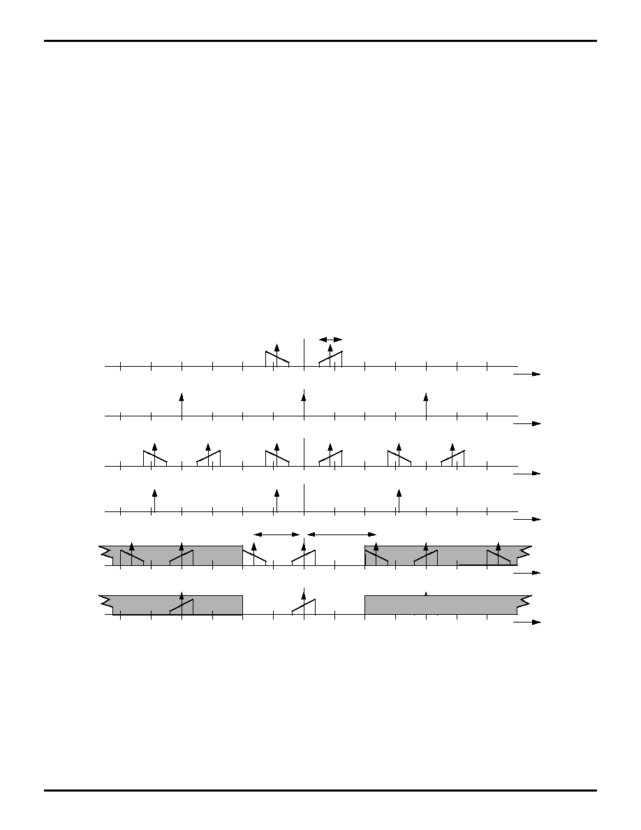
Z87200
Spread-Spectrum Transceiver
Zilog
4-42
THEORY OF OPERATION
The Z87200 receiver's downconverter circuitry allows use
of two distinct modes, where the mode chosen will depend
upon the application. In applications where the received
PN chip rate is less than approximately 1/8 of the I.F. sam-
ple clock (RXIFCLK) rate, the Z87200 can be used with a
single A/D converter (ADC) and operate in Direct I.F. Sam-
pling Mode. For higher chip rate applications, it is neces-
sary to use the Z87200 in the full Quadrature Sampling
Mode; that is, using a quadrature signal source, two ADCs,
and the on-chip NCO in its quadrature mode.
Using the Z87200 with a Single ADC in Direct I.F.
Sample Mode
Direct I.F. Sampling Mode allows one rather than two
ADCs to be used, as will be explained below. If appropriate
for the application, use of Direct I.F. Sampling Mode can
reduce the system cost since quadrature downconversion
with its associated 90
∞
signal separation and the second
ADC used in Quadrature Sampling Mode are not required.
The trade-off, however, is in the lower maximum PN chip
rate that can be supported by the Z87200 in Direct I.F.
Sampling Mode as compared to the maximum rate that
can be supported by Quadrature Sampling Mode.
In Direct I.F. Sampling Mode, the sampled signal is pre-
sented as input to the receiver's I channel input (RXIIN)
and the Q channel input (RXQIN) is held to zero (where
"zero" is defined by the ADC input format ). As a result,
only two of the four multipliers in the Downconverter's
complex multiplier are used and the device does not make
a true single-sideband downconversion from I.F. to base-
band. In Quadrature Sampling Mode, by contrast, quadra-
ture inputs to two ADCs provide I and Q inputs to the
Z87200 and the full complex multiplier is used. An illustra-
tion of the operation of Direct I.F. Sampling Mode is shown
in the frequency domain in Figure 11, where the spectra
have been drawn asymmetrically so that spectral inver-
sions can be readily identified.
Figure 11. Spectra of Signals in Direct I.F. Sampling Mode
FREQ.
INPUT SPECTRUM
BANDWIDTH: B
0
FREQ.
0
FREQ.
SPECTRUM
AFTER A/D
0
FREQ.
SPECTRUM AFTER IDEAL DIGITAL LOW PASS FILTER
0
FREQ.
QUADRATURE
NCO SPECTRUM
0
≠f
1
FREQ.
SPECTRUM AFTER MIXER
0
SPECTRUM OF
SAMPLING PROCESS
2 f
1
f
SA
≠2 f
1
f
SA
1
2
3
4
5
6
≠f
SA
f
SA
≠f
SA
f
SA
≠f
SA
f
SA
≠f
SA
f
SA
≠f
SA
≠f
1
f
1
≠f
1
f
1
PS010202-0601

Z87200
Zilog
Spread-Spectrum Transceiver
4-43
4
The spectrum of a real input signal with center (I.F.) fre-
quency of f1 and signal bandwidth B is shown in line 1 of
Figure 13. The bandwidth B is the two-sided bandwidth,
corresponding to a PN chip rate of 1/2 B Mcps. Note that
throughout this discussion it is assumed that the signal
bandwidth does not exceed 1/2f
SA
; that is, B < 1/2f
SA
. Oth-
erwise, the mixing and sampling processes to be de-
scribed will result in destructive in-band aliasing. Also,
clearly, the I.F. frequency must be able to support the sig-
nal bandwidth; that is, 1/2B<f1.
The input signal is sampled at the frequency f
SA
, where the
sampling spectrum is shown in line 2 and the resulting
spectrum is shown in line 3. As can be seen, the funda-
mental and harmonics of the sampling frequency result in
images of the input signal spectrum at other frequencies,
where here the images are centered about multiples of the
sampling frequency. In other words, the spectrum of the
sampled signal shown in line 3 contains aliases of the input
signal at frequencies f1
±
n f
SA
, where n can assume both
positive and negative integer values. Since the sampling
process is linear, no spectral inversion occurs; that is, the
original spectrum is translated along the frequency axis
with no mirror reflections of the input spectrum created.
The Z87200's NCO provides a quadrature (sine and co-
sine) output that defines a complex signal. Line 4 shows its
spectrum as an impulse at frequency -f1, where the minus
sign reflects the signal's use in downconversion and the
absence of a positive impulse at frequency +f1 results be-
cause the NCO output is truly complex. Aliases of this im-
pulse are shown offset by integer multiples of f
SA
to reflect
the sampled nature of the NCO output. When the input
sampled signal of line 3 is then modulated with the com-
plex signal of the Z87200's quadrature NCO of line 4, the
signal spectrum after mixing is as shown in line 5. The sec-
tions shown inside the shaded areas are the aliases of the
baseband signal beyond the Nyquist frequency and are
not of concern. The signals inside the primary baseband
Nyquist region (| f |<1/2 f
SA
) consist of the desired signal
and a spectrally reversed or inverted image signal with
center frequency separated from that of the desired signal
by 2 f1, twice the I.F. frequency before sampling. This im-
age signal can be removed by a subsequent ideal low-
pass filter as shown in line 6.
In Figure 13, the input signal is shown at a low I.F. frequen-
cy such that f1 < 1/2 f
SA
; that is, the signal is only defined
inside the primary Nyquist region. Provided, however, that
B < 1/2 f
SA
, that condition need not be true as long as the
input spectrum is only defined for frequencies within a non-
primary Nyquist region; that is, defined only over frequen-
cies f such that
(n≠1/2)f
SA
<|f|<(n+1/2)f
SA
for positive integer n.
Direct I.F. Sampling Mode with this type of signal is shown
in Figure 14, where it can be seen that in line 3 the dia-
gram's high frequency input has the same spectrum after
sampling as does the low frequency input in Figure 11;
consequently, all subsequent operations are identical to
those in Figure 13.
This result stems from the periodic nature of sampling:
sampling an input frequency f1 is theoretically indistin-
guishable from sampling an input frequency (n f
SA
+ f1) for
positive integer n and positive f1 < 1/2 f
SA
. A slightly differ-
ent result obtains, however, when sampling an input fre-
quency (n f
SA
- f1), again for positive integer n and positive
f1 < 1/2 f
SA
. In this case, the positions of the spectrally in-
verted and spectrally correct aliases will be interchanged
when compared with an input frequency of (n f
SA
+ f1). As
a consequence, the desired baseband signal after down-
conversion and filtering will also be spectrally inverted.
This phenomenon is equivalent to high-side conversion;
that is, downconversion of a signal by means of a local os-
cillator at a frequency higher than the carrier frequency. If
the modulation type is QPSK, demodulation of a spectrally
inverted signal will result in the inversion of the Q channel
data (which can be readily corrected); if the modulation
type is BPSK, there is no effect on the demodulated data.
PS010202-0601

Z87200
Spread-Spectrum Transceiver
Zilog
4-44
THEORY OF OPERATION (Continued)
The above discussion has assumed ideal low-pass filter-
ing to recover the desired signal at baseband, but, in the
Z87200's Downconverter, an ideal low-pass filter is not
available. The quadrature Integrate and Dump filter of the
Downconverter serves this purpose instead. The Down-
converter's Integrate and Dump filter is a decimation filter,
integrating input samples over a programmable number of
sample periods, N, so that the output sampling rate is
(1/N)th of the input sampling rate and the I.F. sampling rate
fSA is decimated to the baseband sampling rate. Since the
Z87200's PN Matched Filter requires two samples per
chip, the baseband sampling rate must be at twice the PN
chip rate and N must equal f
SA
/B. When the sampling rate
is much greater than the signal bandwidth (or, equivalent-
ly, the chip rate), the Integrate and Dump filter is most ef-
fective in attenuating the unwanted aliased image. This
performance can be seen from the transfer function G(w)
of a decimation filter, where:
G(w) = sin(w')/w' and w' = (2
Nf)/f
SA
.
Figure 13 shows a plot of the gain of this transfer function
as a function of the normalized frequency (N f/F
SA
). To ef-
fect the desired low-pass filter and eliminate the aliased
image in the baseband Nyquist region appearing in line 5
of Figure 11, the attenuation must be suitably high for fre-
quencies greater than, in the worst case, 1/2 B. Given a
defined signal bandwidth B, however, judicious choice of
f1 and f
SA
allows a higher break frequency to be chosen,
as will be discussed.
As an extreme worst case, if f1 = 1/4f
SA
and B=1/2f
SA
, cor-
responding to the highest chip rate that can be handled for
a given value of f
SA
, then the break frequency must be
1/2B (equal to 1/4f
SA
). In this example, then, N = f
SA
/B=2
and the attenuation provided by the Integrate and Dump fil-
ter is given by the curve of Figure 13 for values of (N f/f
SA
)
greater than 1/2. As can be seen, the attenuation will be at
least equal to the peak of the corresponding lobe or at
least ~13 dB. This sidelobe peak is a worst case, and
much of the alias energy outside the desired band will be
attenuated by more than 13 dB. Nonetheless, the pres-
ence of unattenuated energy from the unwanted alias de-
grades performance. It is for this reason that Direct I.F.
Sampling Mode is only recommended for received PN chip
rates less than 1/8 f
SA
; in other words, for B<1/4 f
SA
. The
attenuation realized by the Integrate and Dump filter is
then further determined by the choice of the I.F. frequency
f
1
and the I.F. sampling rate f
SA
.
Figure 12. Direct I.F. Sampling Mode with I.F. Frequency (f
SA
+f
1
) > Sampling Frequency f
SA
FREQ.
INPUT SPECTRUM
BANDWIDTH: B
0
FREQ.
0
FREQ.
SPECTRUM
AFTER A/D
0
SPECTRUM OF
SAMPLING PROCESS
1
2
3
≠f
SA
≠ f
1
f
SA
+ f
1
f
SA
≠f
SA
f
SA
≠f
SA
≠f
1
f
1
PS010202-0601

Z87200
Zilog
Spread-Spectrum Transceiver
4-45
4
The choice of the I.F. frequency and sampling rate is cru-
cial so that the unwanted alias of the signal in the base-
band Nyquist region lies as far as possible from the de-
sired signal to permit maximum attenuation. The optimum
separation of the desired signal and the unwanted alias oc-
curs when the alias is centered at the bounds of the base-
band Nyquist region, | f | =1/2 f
SA
as shown in Figure 14.
In this case, the desired signal is equally spaced from the
unwanted aliases in both the positive and negative fre-
quency domains and f1 = 1/4 f
SA
. Consider, then, the worst
case appropriate for Direct I.F. Sampling Mode. If B<1/4
f
SA
as has been said to be appropriate for Direct I.F. Sam-
pling Mode, then N=f
SA
/B=4, the break frequency is
3 /8 f
SA
or greater, and the attenuation provided by the In-
tegrate and Dump filter is given by the curve of Figure 13
for values of (N f/f
SA
) greater than 3/2. Here, the attenua-
tion is at least ~21 dB, offering much better attenuation of
the unwanted alias than in the previous worst case exam-
ple. Further analysis shows that if the input SNR is 15 dB,
then the alias attenuated by 21 dB will reduce the SNR by
approximately 1 dB.
Figure 13. G(
) = dom (
')/
', where
' = (2
Nf)/f
SA
Figure 14. Optimum Condition for Bandpass Sampling
PS010202-0601

Z87200
Spread-Spectrum Transceiver
Zilog
4-46
THEORY OF OPERATION (Continued)
The optimum choice of I.F. frequency discussed above
can be extended beyond the primary Nyquist region. Since
an I.F frequency of n f
SA
+ f1 produces exactly the same
result for any value of n, the general condition for optimum
separation of the desired signal and the unwanted alias is:
f1 = n f
SA
+ 1 /4 f
SA
and B< 1 /2 f
SA
for positive integer n and positive B and f
1
.
And, if care is taken to handle the effect of high side con-
version, the following I.F. frequencies also fulfill the opti-
mum condition:
f1= n f
SA
1/4 f
SA
and B< 1/2 f
SA
for positive integer n and positive B and f
1
.
Using the Z87200 with Two ADCs in Quadra-
ture Sampling Mode
Quadrature Sampling Mode requires that quadrature I and
Q channel I.F. inputs are sampled by two ADCs and input
to the Z87200's Downconverter. All four multipliers of the
Downconverter's complex multiplier are then used to per-
form true single sideband downconversion to baseband.
Quadrature inputs imply that the input signal is complex,
and the input signal spectrum shown in line 1 of Figure 15
is thus only single-sided with no mirror image spectral
component. As a result, the image alias within the primary
Nyquist region associated with Direct I.F. Sampling Mode
does not appear and does not have to be attenuated by the
Integrate and Dump filter. As in the prior discussion, this
analysis holds as long as B < 1/2 f
SA
, 1/2 B < f1, and the
input spectrum is only defined for frequencies within a sin-
gle Nyquist region; that is, non-zero over frequencies f
such that:
(n≠1/2)f
SA
<|f|<(n+1/2)f
SA
for positive integer n.
Figure 15. Spectra of Signals in Quadrature Sampling Mode
FREQ.
INPUT SPECTRUM
BANDWIDTH: B
0
FREQ.
0
FREQ.
SPECTRUM
AFTER A/D
0
FREQ.
SPECTRUM AFTER IDEAL DIGITAL LOW PASS FILTER
0
FREQ.
QUADRATURE
NCO SPECTRUM
0
≠f
1
FREQ.
SPECTRUM AFTER MIXER
0
SPECTRUM OF
SAMPLING PROCESS
2 f
1
f
SA
≠2 f
1
f
SA
1
2
3
4
5
6
≠f
SA
f
SA
≠f
SA
f
SA
≠f
SA
f
SA
≠f
SA
f
SA
≠f
SA
≠f
1
f
1
≠f
1
f
1
PS010202-0601

Z87200
Zilog
Spread-Spectrum Transceiver
4-47
4
Differential Demodulation
As noted in the preceding text, computation of the "Dot"
and "Cross" products is fundamental to operation of the
DPSK Demodulator and Frequency Discriminator. Let I
k
and Q
k
represent the I and Q channel inputs, respectively,
for the k
th
symbol after downconversion and despreading.
The Dot and Cross products can then be defined as:
Dot(k) = I
k
I
k-1
+ Q
k
Q
k-1
; and,
Cross(k) = Q
k
I
k-1
- I
k
Q
k-1
In the complex domain, these products can be seen to
have been defined to form the complex conjugate product
between two input samples, one symbol apart. Let the k
th
input sample, sin(k), be defined as:
s
in
(k) = I(k) + j Q(k),
where I(k) and Q(k) are the 8-bit peak power PN Matched
Filter I and Q channel outputs directed to the DPSK De-
modulator. In polar form, s
in
(k) may be conveniently de-
fined as:
s
in
(k) = A(k)e
jÿ(k)
with
A(k)
ÿ(k) = arctan
Simple substitution then shows that the complex conjugate
product between consecutive symbols (with an arbitrary
phase shift introduced to the previous symbol value) may
be expressed as:
s
out
(k)= s
in
(k) [s
in
(k≠1) .
fixed
]
*
= Dot(k) + j Cross(k)
where
fixed
= arbitrary fixed phase rotation;
Dot(k)= Re[s
out
(k)]; and,
Cross(k)= Im[s
out
(k)]
*
The fixed phase rotation
fixed
has been introduced to later
simplify the decision criteria. The ability to express real and
imaginary parts of the complex conjugate product between
consecutive symbols with the Dot and Cross products is
the key to their use in DPSK demodulation.
DBPSK Demodulation
In DPSK, the phase difference between successive sam-
ples is due to the data modulation phase differences,
ÿmod, plus any induced phase rotation between sym-
bols,
ÿrot, resulting from, for example, a frequency offset
between the received signal's I.F. and that provided by the
Downconverter. For DBPSK, the data modulation differ-
ences
ÿmod can take only the values of 0
∞
or 180
∞
. Ex-
pressing the complex phase difference [ÿ(k)-ÿ(k-1)] in
terms of these components, the decision can be seen to be
based on:
Sout
(k)
=A(k) A(k-1) e
jÿ(k)*
e
-jÿ(k-1)
=
A(k)
*
A(k1)
*
e
j[
ÿ
mod
(k)+
ÿ
rot
(k)]
For DBPSK, only the real part of sout(k), Dot(k), is needed
to determine the modulated phase transition:
Dot(k)= A(k)
*
A(k-1)
*
cos(
ÿ
mod
(k)+
ÿrot(k))
=
±
A(k)
*
A(k-1)
*
cos(
ÿ
rot
(k))
where the sign is determined by the transmitted data since
cos[
ÿ
mod
(k)] =
±
1
*
As a result,
Dot(k)
±
A
2
(k)
if the amplitude of the signal is constant for consecutive
symbols and if the phase rotation
ÿ
rot
(k) between sym-
bols is small. The Z87200 DPSK Demodulator can thus
use the sign of the Dot product in order to make DBPSK
symbol decisions without the introduction of any fixed
phase rotation.
PS010202-0601

Z87200
Spread-Spectrum Transceiver
Zilog
4-48
THEORY OF OPERATION (Continued)
DQPSK Demodulation
For DQPSK modulation, the possible phase shifts be-
tween successive symbols due to the modulation are 0
∞
,
90
∞
, 180
∞
, and 270
∞
. Here, introduction of a phase shift
(
fixed
) of
±
45
∞
to the previous symbol in the calculation of
the Dot and Cross products is desired in order shift the
possible phase differences to 45
∞
, 135
∞
, 225
∞
, or 315
∞
so
that the DQPSK decision boundaries coincide with the
signs of the Dot and Cross products. In the Z87200 DPSK
demodulator, phase rotation is accomplished in the signal
rotation block by the following transformation of the I and
Q channel values:
I
rot
(k)=[ I(k) - Q(k)]/2 for 45
∞
rotation
I
rot
(k)=[ I(k) + Q(k)]/2 for ≠45
∞
rotation
Q
rot
(k)=[ I(k) + Q(k)]/2 for 45
∞
rotation
Q
rot
(k)=-[ I(k) + Q(k)]/2 for ≠45
∞
rotation
The divide-by-2 is part of the signal rotation function. This
transformation is equivalent to multiplying by (1
±
j)/2 or
(1/
2)e
jÿ(fixed)
where ÿ
fixed
is
±
45
∞
. In this case, s
out
(k) be-
comes:
s
out
(k)=A(k).A(k-1)*e
jÿ(k)*
e
≠jÿ(k-1)*
[
fixed
]*
=A(k).A(k-1)*e
j[
ÿ
mod
(k)+
ÿ
rot
(k)]*
(1/
2)ej
ÿ(fixed)
so that
Dot(k)
(1/
2)A(k)*A(k-1)*cos(
ÿ
mod
(k) - ÿ
fixed
)
Cross(k)
(1/
2)A(k)*A(k-1)*sin(
ÿ
mod
(k) - ÿ
fixed
)
where the phase rotation
ÿ
rot
(k) due to the frequency off-
set between symbols has been assumed negligible.
A summary of the Dot(k) and Cross(k) products for the
possible values of
ÿ
mod
(k) and ÿ
fixed
is shown below, il-
lustrating how the sign of the Dot and Cross products allow
the symbol decision to be made:
/4 QPSK Demodulation
The Z87200 DPSK Demodulator decision logic is de-
signed so that correct DQPSK decisions are made with a
signal rotation of ÿ
fixed
= ≠45
∞
. For
/4 QPSK modulation,
however, the modulator itself inserts 45
∞
between consec-
utive symbols, and the possible phase shifts between suc-
cessive symbols due to modulation are 45
∞
, 135
∞
, 225
∞
,
and 315
∞
. As a result, the DPSK Demodulator should be
configured for
/4 QPSK with ÿ
fixed
=0
∞
.
DQPSK Phasing and I/Q Channel Reversal
The Z87200 uses Differential BPSK and QPSK modulation
and demodulation, meaning that the data is modulated on
the carrier as phase changes. At the demodulator, the data
is recovered by monitoring the phase change over a sym-
bol period.
The Z87200 provides configuration control to specifically
address DPSK phasing and I/Q channel reversal: the Sig-
nal Rotation control register, bits 0 and 1 of address 33
H
,
and the Reverse I and Q control register, bit 0 of address
36
H
. The first register causes an insertion of
±
45
∞
in phase
between consecutive symbols at the receiver, while the
second register switches the I and Q channels presented
to the DPSK demodulator. As discussed in the Z87200 ap-
pendix, the introduction of a phase shift between consec-
utive symbols changes the mapping of the input data with
respect to the decision boundaries defined by the "Cross"
and "Dot" product axes.
Assuming that the transmitted DQPSK modulation phas-
ing is differentially encoded as defined in Table 3, the
phase shift between consecutive symbols should always
be set to ≠45
∞
; that is, bits 1 and 0 of address 33
H
should
be set to 11. Similarly, when the transmission path from
modulator to demodulator does not introduce a frequency
(or phase direction) reversal, the "reverse I and Q" control
function should be disabled; that is, bit 0 of address 36H
should be set to 0. Note that, in the case of DBPSK, the
phase increments are either 0 or 180
∞
and frequency re-
versal has no impact.
If frequency reversal does take place, however, correct
DQPSK demodulation can be achieved by enabling I and
Q reversal; that is, the entry into bit 0 of address 36
H
should be set to 1. Frequency reversal may occur in the up
or down conversion process, depending on which mixing
product is selected for further processing. No reversal oc-
curs when the following conditions exist: when the mixing
(
)
Q(k)
I(k)
.
I
2
(K)+Q
2
(k)
ÿ
fixed
= -45
∞
ÿ
fixed
= +45
∞
ÿ
mod
(k)
Dot(k)
Cross
(k)
ÿ
mod
(k)
Dot(k)
Cross
(k)
0
∞
+A
2
+A
2
0
∞
+A
2
≠A
2
90
∞
≠A
2
+A
2
90
∞
+A
2
+A
2
180
∞
≠A
2
≠A
2
180
∞
≠A
2
+A
2
270
∞
+A
2
≠A
2
270
∞
≠A
2
≠A
2
PS010202-0601

Z87200
Zilog
Spread-Spectrum Transceiver
4-49
4
at the transmitter is performed by processing the sum fre-
quency of the local oscillator and the modulator; when the
mixing at the receiver is performed by subtracting the local
oscillator from the incoming signal; and when the in-phase
and quadrature inputs into the I and Q analog-to-digital
converters are correctly connected such that the in-phase
component leads the quadrature component by 90
∞
. Un-
der these conditions, bit 0 of address 36
H
should be set to
0; otherwise, the I and Q channels may need to be re-
versed at the DPSK demodulator (by setting bit 0 of ad-
dress 36
H
to 1) in order to achieve proper demodulation.
Frequency Error Signal Generation
The frequency discriminator function or error signal is gen-
erated based on the Dot and Cross products. The objec-
tive is an error signal that is proportional to the sine of the
phase difference between the present and prior symbol af-
ter correcting for the estimated phase increments due to
data modulation. In the Z87200 Frequency Discriminator,
the frequency error is calculated through a decision-direct-
ed cross-product algorithm and is then used with the Loop
Filter to correct the NCO frequency. Assuming an input
sin(k), where:
s
in
(k) =
I(k) + j Q(k),
the algorithm calculates the frequency discriminator func-
tion for DBPSK, s
AFC/BPSK
(k), as:
S
AFC/BPSK
(k)=SIGN[Dot(k)]*Cross(k)
=SIGN[Dot(k)]*A(k)*A(k-1)*sin(ÿ(k)-ÿ(k-1))
=SIGN[Dot(k)]*A(k)*A(k-1)*sin(
ÿmod(k) +
ÿrot(k))
SIGN[Dot(k)]*A2(k)*cos[
ÿmod(k)]*sin[
ÿrot(k)]
A2(k)*sin[
ÿrot(k)]*
The final result assumes that the amplitude of the signal is
constant over consecutive symbols and shows that the
discriminator function is directly related to the change in
phase between successive symbols. Since the interval be-
tween successive symbols is fixed, the discriminator func-
tion can be interpreted as a frequency error signal.
For DQPSK signals, the Z87200 computes the discrimina-
tor function S
AFC/QPSK
(k) as:
S
AFC/QPSK(
k)=SIGN[Dot(k)] Cross(k) - SIGN[Cross(k)]
Dot(k),
where the above expression can be reduced to the same
as for DBPSK,
S
AFC/QPSK
(k)
A2(k)*sin(
ÿrot(k)).
BPSK/QPSK Modulation
The Z87200 incorporates a Direct Digital Synthesizer
(DDS) to implement its on-chip BPSK/QPSK modulator. In
the Z87200 design, the NCO and thus the sampling clock
for the modulator is driven by fRXIFCLK; for this reason,
both TXIFCLK and RXIFCLK must be common if the on-
chip BPSK/QPSK modulator is to be used. The
BPSK/QPSK modulator can then be used to generate the
transmit output signal at a programmable IF frequency,
thereby eliminating the need for an external modulator.
Because it is a sampled data system like the Downconvert-
er of the Z87200, however, care must be taken to ensure
that the results of aliasing do not adversely affect the out-
put transmit signal.
PS010202-0601

Z87200
Spread-Spectrum Transceiver
Zilog
4-50
THEORY OF OPERATION (Continued)
In general, when a DDS is used to generate an unmodu-
lated signal, the stepped sine wave generated by the DDS
has spectral components at integer multiples of the DDS
sampling clock. In other words, the Z87200's BPSK/QPSK
modulator, when programmed to generate a signal at I.F.
frequency f
OUT
, will produce spectral components at
±
f
OUT
as well as at (n
RXIFCLK
±
f
OUT
), where n is a positive or
negative integer. Because of these aliases, one generally
cannot program the NCO to provide an output frequency
f
OUT
greater than the Nyquist frequency f
RXIFCLK/2
. When
the I.F. frequency f
OUT
is modulated, however, degrada-
tions to the output signal due to aliasing can result even
when f
OUT
is less than f
RXIFCLK/2
.
In particular, the Z87200's PN modulation results in a
transmit signal that has a power spectral density charac-
terizable as a sinc function (sin(x)/x) centered about the
I.F. frequency f
OUT
. Nulls of the sinc function occur at inte-
ger multiples of the PN chip rate, and the null-to-null signal
bandwidth of the Z87200's transmit signal about f
OUT
is
twice the transmit chip rate. The presence of modulation
sidelobes and their interaction with aliases due to sam-
pling, however, will result in distortion of the mainlobe of
the baseband component centered at f
OUT
unless atten-
tion is paid to the interaction of the chip rate, the I.F. fre-
quency f
OUT
, and the sampling rate fRXIFCLK.
In the example of Figure 18, the spectrum drawn in bold
represents a signal where f
OUT
has been programmed to
be (0.4 x f
RXIFCLK
) and has been PN-modulated at a chip
rate of (0.1 x f
RXIFCLK
). The first alias of the negative fre-
quency version of this signal appears centered about (0.6
x f
RXIFCLK
) and is shown as the lighter curve. As can be
seen, energy of the second and third modulation sidelobes
of the first alias is present within the mainlobe of the base-
band component, resulting in distortion. One would typical-
ly filter the digital-to-analog converted output of the
Z87200's BPSK/QPSK modulator to remove the energy
outside the modulation mainlobe, but such filtering will not
affect any aliasing distortion within the mainlobe as de-
scribed here. Note that the nulls of the modulated signal
aliases in this example coincide here only due to the
choice of values for the I.F. frequency, sampling rate, and
PN chip rate; in general, the nulls will not coincide. Note
also that the filtering effect of sampling has been neglected
in this discussion -- in general, the aliases will be sup-
pressed by a second sinc function, sin(f')/(f'), where f' =
f/f
RXIFCLK
, but this effect is not very significant for the
baseband component and first alias.
Figure 16. Spectrum of DDS modulated at 0.1 x f
RXIFCLK
when carrier frequency is set to 0.4 x f
RXIFCLK
PS010202-0601
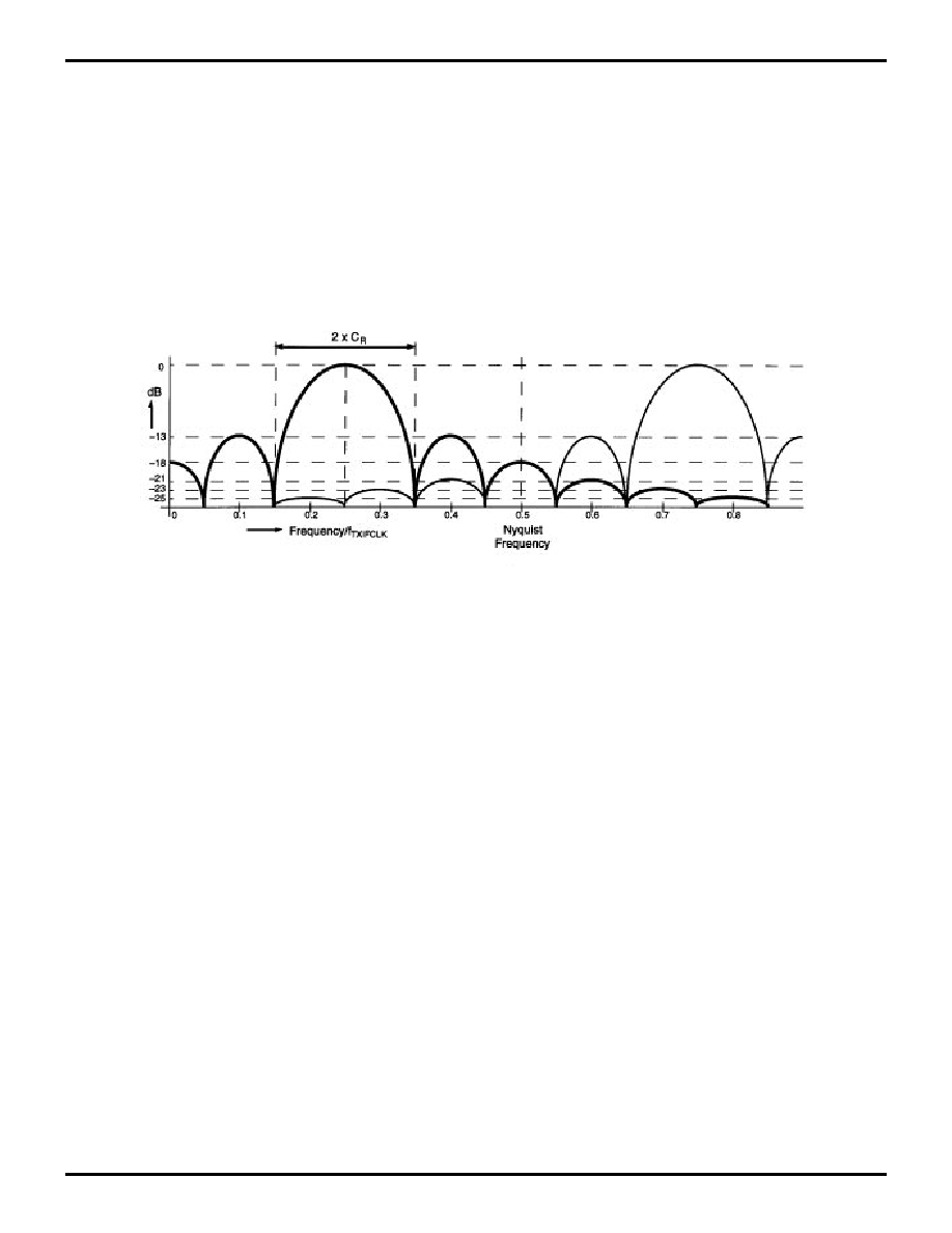
Z87200
Zilog
Spread-Spectrum Transceiver
4-51
4
The example of Figure 18 demonstrates that aliasing dis-
tortion of the BPSK/QPSK modulator output will result if
significant energy of the baseband component's spectrum
falls beyond the Nyquist frequency of f
RXIFCLK/2
. The first
alias will then shift that energy into the region below the
Nyquist frequency and potentially interfere with the desired
signal. In Figure 19 the second and third sidelobes of the
first alias fall within the mainlobe of the baseband compo-
nent, where the magnitude of this corrupting signal is ap-
proximately ≠13 dBc.
In Figure 20, by contrast, the level of distortion is consider-
ably reduced by programming an I.F. frequency that in-
creases the separation of the baseband mainlobe from the
alias mainlobe. Here, the carrier frequency has been re-
duced to 0.25 x f
RXIFCLK
, and now the fourth and fifth side-
lobes of the first alias lie in the same part of the spectrum
as the baseband mainlobe, reducing the distorting energy
to approximately ≠23 dBc at the peak of the fourth side-
lobe.
Figure 17. Spectrum of DDS modulated at 0.1 x f
RXIFCLK
when carrier frequency is set to 0.25 x f
RXIFCLK
PS010202-0601

Z87200
Spread-Spectrum Transceiver
Zilog
4-52
THEORY OF OPERATION (Continued)
In both of the cases shown above, and especially the sec-
ond, the level of the distortion is low enough so that the
performance penalty would not be very great. And, of
course, in a spread-spectrum system the effective distor-
tion is reduced by the processing gain realized in de-
spreading the signal at the receiver. In both of these exam-
ples, however, the PN chip rate is a very modest 10% of
the frequency of the system clock; if the chip rate is in-
creased to 40% of f
RXIFCLK
, then the situation is very dif-
ferent, as shown in Figure 20.
In Figure 20, both the chip rate and the carrier frequency
have been set at 40% of the clock frequency. As a result,
the baseband mainlobe straddles the Nyquist frequency,
and the first alias of the mainlobe overlaps the spectrum of
the baseband mainlobe, thereby creating very significant
aliasing distortion which cannot be eliminated by filtering.
This level of distortion would severely affect the perfor-
mance of the system and, in general, would be completely
unacceptable.
Figure 18. Spectrum of DDS Modulated at 0.4 x f
RXIFCLK
When Carrier Frequency is set to 0.4 x f
RXIFCLK
PS010202-0601

Z87200
Zilog
Spread-Spectrum Transceiver
4-53
4
Reducing the carrier frequency to 25% of the clock fre-
quency can reduce the distortion level, as shown in Figure
21. Although the distortion is still fairly severe, adequate
performance may be obtainable as a result of the system's
processing gain, but the performance would be many dB
off the theoretical limit. As the PN chip rate of the system
increases, then so, too, does the effect of aliasing distor-
tion in the modulator, resulting in performance degrada-
tion. As a rule-of-thumb, one may restrict the I.F. frequency
to 25% of the clock frequency, but, in general, each appli-
cation and combination of PN chip rate, I.F. frequency, and
TXIFCLK/RXIFCLK frequency is unique and should be
evaluated before deciding whether to use the Z87200's in-
ternal BPSK/QPSK modulator.
Figure 19. Spectrum of DDS Modulated at 0.4 x f
RXIFCLK
When Carrier Frequency is set to 0.25 x f
RXIFCLK
PS010202-0601