
ZiLOG Worldwide Headquarters ∑ 532 Race Street ∑ San Jose, CA 95126-3432
Telephone: 408.558.8500 ∑ Fax: 408.558.8300 ∑
www.ZiLOG.com
Product Specification
Z87C33
CMOS Z8
Æ
MCU Consumer
Controller Processor
PS015601-1003

PS015601-1003
©2003 by ZiLOG, Inc. All rights reserved. Information in this publication concerning the devices, applica-
tions, or technology described is intended to suggest possible uses and may be superseded. ZiLOG, INC.
DOES NOT ASSUME LIABILITY FOR OR PROVIDE A REPRESENTATION OF ACCURACY OF
THE INFORMATION, DEVICES, OR TECHNOLOGY DESCRIBED IN THIS DOCUMENT. ZiLOG
ALSO DOES NOT ASSUME LIABILITY FOR INTELLECTUAL PROPERTY INFRINGEMENT
RELATED IN ANY MANNER TO USE OF INFORMATION, DEVICES, OR TECHNOLOGY
DESCRIBED HEREIN OR OTHERWISE. Except with the express written approval of ZiLOG, use of
information, devices, or technology as critical components of life support systems is not authorized. No
licenses are conveyed, implicitly or otherwise, by this document under any intellectual property rights.

PS015601-1003
Table of Contents
Z87C33
CMOS Z8" MCU Consumer Controller Processor
iii
Table of Contents
Architectural Overview . . . . . . . . . . . . . . . . . . . . . . . . . . . . . . . . . . . . . . . . . . . . 1
Features . . . . . . . . . . . . . . . . . . . . . . . . . . . . . . . . . . . . . . . . . . . . . . . . . . . . 2
Functional Block Diagram . . . . . . . . . . . . . . . . . . . . . . . . . . . . . . . . . . . . . . . 3
Pin Description . . . . . . . . . . . . . . . . . . . . . . . . . . . . . . . . . . . . . . . . . . . . . . . . . . 4
Pin Functions . . . . . . . . . . . . . . . . . . . . . . . . . . . . . . . . . . . . . . . . . . . . . . . . . . . . 5
Control Registers . . . . . . . . . . . . . . . . . . . . . . . . . . . . . . . . . . . . . . . . . . . . . . . . 32
Expanded Register File, Bank 0h . . . . . . . . . . . . . . . . . . . . . . . . . . . . . . . . 32
Timer Mode Register . . . . . . . . . . . . . . . . . . . . . . . . . . . . . . . . . . . . . . . . . . 32
Expanded Register File, Bank Fh . . . . . . . . . . . . . . . . . . . . . . . . . . . . . . . . 42
Electrical Characteristics . . . . . . . . . . . . . . . . . . . . . . . . . . . . . . . . . . . . . . . . . . 47
Absolute Maximum Ratings . . . . . . . . . . . . . . . . . . . . . . . . . . . . . . . . . . . . . 47
DC Electrical Characteristics . . . . . . . . . . . . . . . . . . . . . . . . . . . . . . . . . . . . 49
AC Electrical Characteristics . . . . . . . . . . . . . . . . . . . . . . . . . . . . . . . . . . . . 56
Standard Test Conditions . . . . . . . . . . . . . . . . . . . . . . . . . . . . . . . . . . . . . . 61
Capacitance . . . . . . . . . . . . . . . . . . . . . . . . . . . . . . . . . . . . . . . . . . . . . . . . 61
Packaging . . . . . . . . . . . . . . . . . . . . . . . . . . . . . . . . . . . . . . . . . . . . . . . . . . . . . 61
Ordering Information . . . . . . . . . . . . . . . . . . . . . . . . . . . . . . . . . . . . . . . . . . . . . 63
Part Number Description . . . . . . . . . . . . . . . . . . . . . . . . . . . . . . . . . . . . . . . 64
Document Information . . . . . . . . . . . . . . . . . . . . . . . . . . . . . . . . . . . . . . . . . . . . 65
Document Number Description . . . . . . . . . . . . . . . . . . . . . . . . . . . . . . . . . . 65
Customer Feedback Form . . . . . . . . . . . . . . . . . . . . . . . . . . . . . . . . . . . . . . . . . 65
Z87C33 Product Specification . . . . . . . . . . . . . . . . . . . . . . . . . . . . . . . . . . . 65
Product Information . . . . . . . . . . . . . . . . . . . . . . . . . . . . . . . . . . . . . . . . . . . 66
Return Information . . . . . . . . . . . . . . . . . . . . . . . . . . . . . . . . . . . . . . . . . . . . 66

PS015601-1003
List of Figures
Z87C33
CMOS Z8" MCU Consumer Controller Processor
iv
List of Figures
Figure 1. Functional Block Diagram . . . . . . . . . . . . . . . . . . . . . . . . . . . . . . . . . 3
Figure 2. 28-Pin DIP/SOIC Pin Configuration . . . . . . . . . . . . . . . . . . . . . . . . . 4
Figure 3. Port 0 Configuration . . . . . . . . . . . . . . . . . . . . . . . . . . . . . . . . . . . . . . 6
Figure 4. Port 2 Configuration . . . . . . . . . . . . . . . . . . . . . . . . . . . . . . . . . . . . . . 7
Figure 5. Port 3 Configuration . . . . . . . . . . . . . . . . . . . . . . . . . . . . . . . . . . . . . . 9
Figure 6. Port 3 Configuration--PCON Register Detail . . . . . . . . . . . . . . . . . 10
Figure 7. Program Memory Map . . . . . . . . . . . . . . . . . . . . . . . . . . . . . . . . . . . 12
Figure 8. Register Pointer--Detail . . . . . . . . . . . . . . . . . . . . . . . . . . . . . . . . . 14
Figure 9. Expanded Register File Architecture . . . . . . . . . . . . . . . . . . . . . . . . 16
Figure 10. Counter/Timer Block Diagram . . . . . . . . . . . . . . . . . . . . . . . . . . . . . 17
Figure 11. Interrupt Block Diagram . . . . . . . . . . . . . . . . . . . . . . . . . . . . . . . . . . 18
Figure 12. Oscillator Configuration . . . . . . . . . . . . . . . . . . . . . . . . . . . . . . . . . . 20
Figure 13. Stop-Mode Recovery Source . . . . . . . . . . . . . . . . . . . . . . . . . . . . . . 25
Figure 14. Resets and Watch-Dog Timer Example . . . . . . . . . . . . . . . . . . . . . . 30
Figure 15. Typical Low-Voltage Protection vs. Temperature . . . . . . . . . . . . . . 31
Figure 16. Additional Timing . . . . . . . . . . . . . . . . . . . . . . . . . . . . . . . . . . . . . . . 56
Figure 17. Test Load Diagram . . . . . . . . . . . . . . . . . . . . . . . . . . . . . . . . . . . . . . 61
Figure 18. 28-Pin DIP Package Diagram . . . . . . . . . . . . . . . . . . . . . . . . . . . . . 62
Figure 19. 28-Pin SOIC Package Diagram . . . . . . . . . . . . . . . . . . . . . . . . . . . . 63

PS015601-1003
List of Tables
Z87C33
CMOS Z8" MCU Consumer Controller Processor
v
List of Tables
Table 1. Family Features . . . . . . . . . . . . . . . . . . . . . . . . . . . . . . . . . . . . . . . . . . . 2
Table 2. 28-Pin DIP/SOIC Pin Configuration . . . . . . . . . . . . . . . . . . . . . . . . . . . . 4
Table 3. Port 3 Pin Assignments . . . . . . . . . . . . . . . . . . . . . . . . . . . . . . . . . . . . . 8
Table 4. Register Pointer Register--RP FDh/R253 Bank 0h: READ/WRITE . . 13
Table 5. Interrupt Types, Sources, and Vectors. . . . . . . . . . . . . . . . . . . . . . . . . 18
Table 6. IRQ Register* . . . . . . . . . . . . . . . . . . . . . . . . . . . . . . . . . . . . . . . . . . . . 19
Table 7. Port Configuration Register--PCON 00h/R0 Bank Fh: WRITE ONLY. 22
Table 8. Stop-Mode Recovery Register 1--SMR1 0Bh/R11 Bank Fh: WRITE
ONLY, except Bit D7, which is READ ONLY . . . . . . . . . . . . . . . . . . 23
Table 9. Stop-Mode Recovery Source . . . . . . . . . . . . . . . . . . . . . . . . . . . . . . . . 26
Table 10. Stop-Mode Recovery Register 2 . . . . . . . . . . . . . . . . . . . . . . . . . . . . 26
Table 11. Stop-Mode Recovery Register 2--SMR2 0Dh/R13 Bank Fh: WRITE
ONLY . . . . . . . . . . . . . . . . . . . . . . . . . . . . . . . . . . . . . . . . . . . . . . . . 27
Table 12. Watch-Dog Timer Mode Register--WDTMR 0Fh/R15: WRITE
ONLY . . . . . . . . . . . . . . . . . . . . . . . . . . . . . . . . . . . . . . . . . . . . . . . . 28
Table 13. WDT Time Select . . . . . . . . . . . . . . . . . . . . . . . . . . . . . . . . . . . . . . . 28
Table 14. Maximum (V
LV
) Conditions: . . . . . . . . . . . . . . . . . . . . . . . . . . . . . . . . 31
Table 15. Expanded Register File Registers--Reset States . . . . . . . . . . . . . . . 32
Table 16. Timer Mode Register--TMR F1h/R241 Bank 0h: READ/WRITE. . . . 33
Table 17. Counter/Timer 1 Register--T1 F2h/R242 Bank 0h: READ/WRITE . . 33
Table 18. Prescaler 1 Register--PRE1 F3h/R243 Bank 0h: WRITE ONLY . . . 34
Table 19. Counter/Timer 0 Register--T0 F4h/R244 Bank 0h: READ/WRITE . . 35
Table 20. Prescaler 0 Register--PRE0 F5h/R245 Bank 0h: WRITE ONLY . . . 35
Table 21. Port 2 Mode Register--P2M F6h/R246 Bank 0h: WRITE ONLY . . . . 36
Table 22. Port 3 Mode Register--P3M F7h/R247 Bank 0h: WRITE ONLY . . . . 36
Table 23. Ports 0 and 1 Mode Register--P01M F8h/R248 Bank 0h: WRITE
ONLY. . . . . . . . . . . . . . . . . . . . . . . . . . . . . . . . . . . . . . . . . . . . . . . . 37
Table 24. Interrupt Priority Register--IPR F9h/R249 Bank 0h: WRITE ONLY . 37
Table 25. Interrupt Request Register--IRQ FAh/R250 Bank 0h: READ/WRITE 38
Table 26. Interrupt Mask Register--IMR FBh/R251 Bank 0h: READ/WRITE . . 39
Table 27. Flags Register--FLAGS FCh/R252 Bank 0h: READ/WRITE. . . . . . . 40
Table 28. Register Pointer--RP FDh/R253 Bank 0h: READ/WRITE. . . . . . . . . 41
Table 29. General Purpose--GPR FEh/R254 Bank 0h: READ/WRITE. . . . . . . 41
Table 30. Stack Pointer Low--SPL FFh/R255 Bank 0h: READ/WRITE . . . . . . 42
Table 31. Expanded Register File Registers--Reset States . . . . . . . . . . . . . . . 42

PS015601-1003
List of Tables
Z87C33
CMOS Z8" MCU Consumer Controller Processor
vi
Table 32. Port Configuration Register--PCON 00h/R0 Bank Fh: WRITE ONLY 43
Table 33. Stop-Mode Recovery Register--SMR 0Bh/R11 Bank Fh:
READ/WRITE . . . . . . . . . . . . . . . . . . . . . . . . . . . . . . . . . . . . . . . . . . 44
Table 34. Stop-Mode Recovery Register 2--SMR2 0Dh/R13 Bank Fh: WRITE
ONLY . . . . . . . . . . . . . . . . . . . . . . . . . . . . . . . . . . . . . . . . . . . . . . . . 46
Table 35. Watch-Dog Timer Mode Register--WDTMR 0Fh/R15 Bank Fh: WRITE
ONLY . . . . . . . . . . . . . . . . . . . . . . . . . . . . . . . . . . . . . . . . . . . . . . . . 46
Table 36. Absolute Maximum Ratings . . . . . . . . . . . . . . . . . . . . . . . . . . . . . . . . 47
Table 37. DC Electrical Characteristics at Standard Temperature. . . . . . . . . . . 49
Table 38. DC Electrical Characteristics at Extended Temperature . . . . . . . . . . 53
Table 39. Additional Timing at Standard Temperature. . . . . . . . . . . . . . . . . . . . 57
Table 40. Additional Timing at Extended Temperature . . . . . . . . . . . . . . . . . . . 59
Table 41. Capacitance* . . . . . . . . . . . . . . . . . . . . . . . . . . . . . . . . . . . . . . . . . . . 61
Table 42. Ordering Information . . . . . . . . . . . . . . . . . . . . . . . . . . . . . . . . . . . . . 63

PS015601-1003
Z87C33
CMOS Z8" MCU Consumer Controller Processor
1
Architectural Overview
ZiLOG's large Z8
Æ
family of 8-bit microcontrollers now includes the Z87C33 prod-
uct line, featuring an enhanced wake-up circuitry, programmable Watch-Dog Tim-
ers (WDT), and low-noise/EMI options. These enhancements to the Z8 offers a
more efficient, cost-effective design and provides the user with increased design
flexibility over the standard Z8 microcontroller core. The low-power-consumption
CMOS microcontroller offers fast execution, efficient use of memory, sophisticated
interrupts, input/output bit manipulation capabilities, and easy hardware/software
system expansion.
The Z87C33 subfamily features an Expanded Register File (ERF) to allow access
to register-mapped peripheral and I/O circuits. Four basic address spaces are
available to support this wide range of configurations: Program Memory, Register
File, and ERF. The Register File is composed of 237 bytes of general-purpose
registers, three I/O port registers, 15 control and status registers. The ERF con-
sists of four control registers.
For applications demanding powerful I/O capabilities, the Z87C33 offers 24 pins
dedicated to input and output. These lines are configurable under software con-
trol.
The Z87C33 family operates at 4MHz with a voltage range of 3.0 to 5.5V
DC
.
To unburden the system from coping with real-time tasks such as counting/timing,
the Z8 offers two on-chip counter/timers with a large number of user-selectable
modes.
All signals with an overline are active Low. For example, B/W,
for which WORD is active Low, and B/W, for which BYTE is
active Low.
Power connections follow these conventional descriptions:
Connection
Circuit
Device
Power
V
CC
V
DD
Ground
GND
V
SS
Note:

PS015601-1003
Z87C33
CMOS Z8" MCU Consumer Controller Processor
2
Features
∑
28-Pin DIP and 28-Pin SOIC
∑
3.0- to 5.5-Volt Operating Range
∑
Operating Temperature Ranges:
Standard: 0∫C to 70∫C
Extended: ≠40∫C to +105∫C
∑
Expanded Register File (ERF)
∑
24 Input/Output Lines
∑
Vectored, Prioritized Interrupts with Programmable Polarity
∑
Two Analog Comparators
∑
Two Programmable 8-Bit Counter/Timers, each with two 6-Bit Programmable
Prescalers
∑
VBO/Power-On Reset (POR)
∑
Clock-Free Watch-Dog Timer (WDT) Reset
∑
On-Chip Oscillator that accepts a Crystal, Ceramic Resonator, LC, RC, or Exter-
nal Clock
∑
RAM and ROM Protect
Table 1. Family Features
Device
ROM (KB) RAM* (Bytes) Speed (MHz--Standard and Extended Temperature)
Z87C33 4
236
4
Note: *General-Purpose.

PS015601-1003
Z87C33
CMOS Z8" MCU Consumer Controller Processor
3
Functional Block Diagram
Figure 1. Functional Block Diagram
Two Analog
Comparators
Interrupt
Control
Port 3
Counter/
Program
Counter
Timers (2)
Machine
Timing & Inst.
ALU
Control
FLAG
Register
Pointer
Port 2
Port 0
I/O
(Bit Programmable)
Address or I/O
V
CC
GND
XTAL
(Nibble Programmable)
4
4
Register File
Output Input
Prg. Memory
4K
RESET
WDT, POR

PS015601-1003
Z87C33
CMOS Z8" MCU Consumer Controller Processor
4
Pin Description
Figure 2.28-Pin DIP/SOIC Pin Configuration
Table 2. 28-Pin DIP/SOIC Pin Configuration
Pin #
Symbol
Function
Direction
1≠3
P25-27
Port 2, Pins 5,6,7
Input/Output
4-7
P04-07
Port 0, Pins 4-7
Input/Output
8
V
DD
Power Supply
9
XTAL2
Crystal Oscillator
Output
10
XTAL1
Crystal Oscillator
Input
11-13
P31-33
Port 3, Pins 1,2,3
Fixed Input
14-15
P34-35
Port 3, Pins 4,5
Fixed Output
16
P37
Port 3, Pin 7
Fixed Output
17
P36
Port 3, Pin 6
Fixed Output
18
P30
Port 3, Pin 0
Fixed Input
19-21
P00-02
Port 0, Pins 0,1,2
Input/Output
22
V
SS
Ground
23
P03
Port 0, Pin 3
Input/Output
24-28
P20-24
Port 2, Pins 0,1,2,3,4
Input/Output
P25
P26
P27
P04
P05
P06
P07
V
DD
XTAL2
XTAL1
P31
P32
P33
P34
P24
P23
P22
P21
P20
P03
VSS
P02
P01
P00
P30
P36
P37
P35
1
2
3
4
5
6
7
8
9
10
11
12
13
14
28
27
26
25
24
23
22
21
20
19
18
17
16
15

PS015601-1003
Z87C33
CMOS Z8" MCU Consumer Controller Processor
5
Pin Functions
The following pages describe the function of each available Z87C33 family pin.
X
IN
Crystal Input.
This pin connects a parallel-resonant crystal, ceramic resonator,
LC, or RC network, or an external single-phase clock to the on-chip oscillator
input.
X
OUT
Crystal Output.
This pin connects a parallel-resonant crystal, ceramic reso-
nant, LC, or RC network to the on-chip oscillator output.
Port 0 (P00≠P07).
Port 0 is an 8-bit, bidirectional, CMOS-compatible port. These
eight I/O lines are configured under software control as a nibble I/O port (P03≠P00
input/output and P07≠P04 input/output), or as an address port for interfacing
external memory. The input buffers are Schmitt-triggered and nibble-programmed
as outputs and can be globally programmed as either push-pull or open-drain.
Low-EMI output buffers are globally programmed by the software.
PS015601-1003
Z87C33
CMOS Z8" MCU Consumer Controller Processor
6
Figure 3. Port 0 Configuration
Port 2 (P27≠P20).
Port 2 is an 8-bit, bidirectional, CMOS-compatible I/O port.
These eight I/O lines are configured under software control as an input or output,
independently. Port 2 is always available for I/O operation. The input buffers are
Schmitt-triggered. Bits programmed as outputs may be globally programmed as
either push-pull or open-drain. Low-EMI output buffers are globally programmed
by the software. See Figure 5.
OE
Out
In
PAD
Auto Latch
1.5
2.3 Hysteresis V
CC
@ 5.0V
R ~~ 500 k
Port 0
(Mask Option)
Open-Drain
(I/O)
Z8
4
4
PS015601-1003
Z87C33
CMOS Z8" MCU Consumer Controller Processor
7
Figure 4.Port 2 Configuration
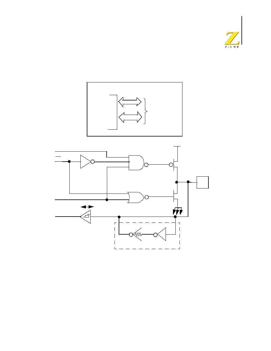
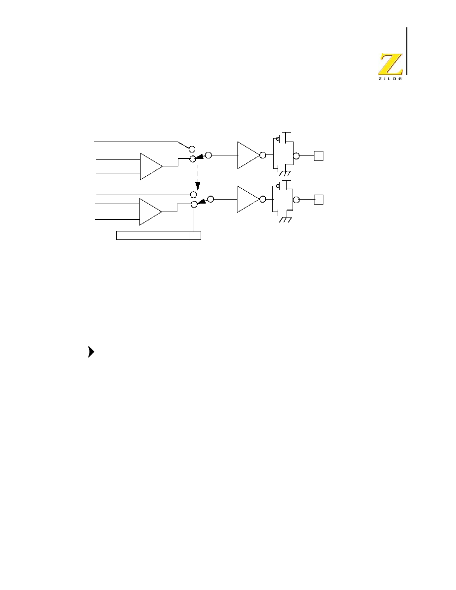
Port 3 (P37≠P30).
Port 3 is an 8-bit, CMOS-compatible port, with four fixed inputs
(P33≠P30) and four fixed outputs (P34≠P37). Port 3 is configured under software
control for Input/Output, Counter/Timers, interrupt, and UART. Port 3, bit 0 input is
Schmitt-triggered, and pins P31, P32, and P33 are standard CMOS inputs (no
autolatches). Pins P34, P35, P36, P37 are push-pull output lines. Low-EMI output
buffers are globally programmed by the software.
Two onboard comparators process analog signals on P31 and P32 with reference
to the voltage on P33. The analog function is enabled by programming Port 3
Z8
Port 2 (I/O)
Open
Out
In
PAD
Auto Latch
1.5
2.3 Hysteresis V
CC
@ 5.0V
R ~
~ 500 k
Open Drain
(Mask Option)
PS015601-1003
Z87C33
CMOS Z8" MCU Consumer Controller Processor
8
Mode Register (P3M bit 1). For interrupt functions, Port 3, bit 0 and pin 3 are fall-
ing-edge interrupt inputs. P31 and P32 are programmable as rising, falling, or
both edge-triggered interrupts (IRQ register bits 6 and 7). P33 is the comparator
reference voltage input when in Analog mode. Access to Counter/Timer 1 is made
through P31 (T
IN
) and P36 (T
OUT
). Handshake lines for Ports 0, 1, and 2 are avail-
able on P31 through P36.
Port 3 also provides the following control functions: four external interrupt request
signals (IRQ3≠IRQ0) and timer input and output signals (T
IN
and T
OUT
).
Comparator Inputs and Outputs.
Port 3, pins P31 and P32 each feature a compar-
ator front end. The comparator reference voltage, pin P33, is common to both
comparators. In ANALOG mode, the P31 and P32 are the positive inputs to the
comparators, and P33 is the reference voltage supplied to both comparators. In
DIGITAL mode, pin P33 is used as a P33 register input or IRQ1 source. P34 and
P37 can provide the comparator output directly by software-programming the
PCON register bit D0 to 1 (see Figure 5).
The user must add a two-NOP delay after setting the P3M bit
D1 to 1 before the comparator output is valid. IRQ0, IRQ1, and
IRQ2 must be cleared in the IRQ register when the comparator
is enabled or disabled.
Table 3. Port 3 Pin Assignments
Pin
I/O
Control
Timer
Analog
Interrupt
P30
IN
IRQ3
P31
IN
T
IN
AN1
IRQ2
P32
IN
AN2
IRQ0
P33
IN
REF
IRQ1
P34
OUT
AN1≠OUT
P35
OUT
P36
OUT
T
OUT
P37
OUT
AN2≠OUT
Note:
PS015601-1003
Z87C33
CMOS Z8" MCU Consumer Controller Processor
9
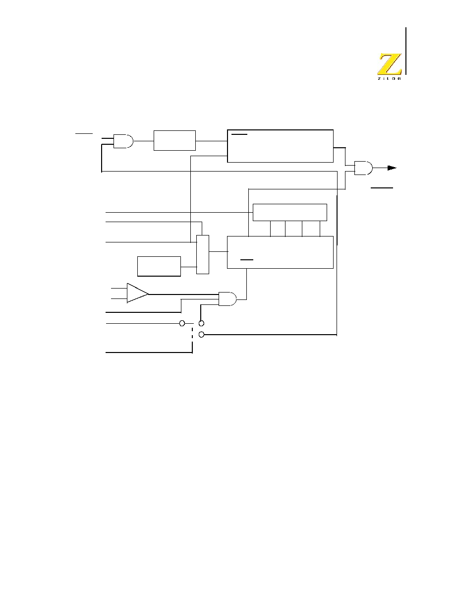
Figure 5. Port 3 Configuration
+
-
+
-
IRQ2, TIN, P31 Data Latch
IRQ0, P32 Data Latch
IRQ1, P33 Data Latch
P31 (AN1)
P32 (AN2)
P33 (REF)
D1
R247 = P3M
DIG.
ANL.
Port 3
0 = Digital
1 = Analog
P30
Auto Latch
(Programmable Option)
P30 Data
Latch IRQ3
(I/O or
Control)
Z8
From Stop-Mode
Recovery Source
PS015601-1003
Z87C33
CMOS Z8" MCU Consumer Controller Processor
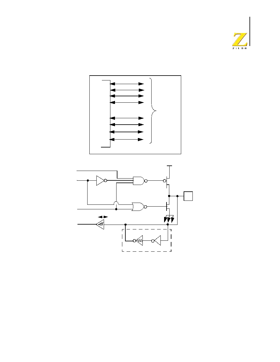
10
Figure 6.Port 3 Configuration--PCON Register Detail
Autolatch.
The autolatch places valid CMOS levels on all CMOS inputs (except
P33≠P31) that are not externally driven. Whether this level is 0 or 1 cannot be
determined. A valid CMOS level, rather than a floating node, reduces excessive
supply current flow in the input buffer. Autolatches are available on Port 0, Port 1,
Port 2, and P30. There are no auto latches on P31, P32, and P33.
Deletion of all port autolatches is available as an option when
the device is programmed. The AUTOLATCH DISABLE option
is selected by the customer when the device is programmed.
D0
PCON
P31
P34 OUT
+
-
REF (P33)
PAD
PAD
P34
P37
0 P34, P37 Standard Output
1 P34, P37 Comparator Output
REF (P33)
P32
P37 OUT
+
-
Note:

PS015601-1003
Z87C33
CMOS Z8" MCU Consumer Controller Processor
11
Functional Description
The Z8 MCU incorporates the following functions that enhance the standard Z8
Æ
architecture and provide the user with increased design flexibility:
∑
Program Memory
∑
ROM Protect
∑
RAM Protect
∑
Working Register File
∑
Expanded Register File
∑
General-Purpose Registers
∑
Stack Pointer
∑
Counter/Timers
∑
Interrupts
∑
Clock
∑
Power-On Reset
∑
HALT and STOP Modes
∑
Port Configuration Register
∑
Comparator
∑
Stop-Mode Recovery
∑
Watch-Dog Timer
∑
Voltage Comparator (V
LV
)
RESET.
The device is reset in one of the following conditions.
∑
Power-On Reset
∑
Watch-Dog Timer
∑
Stop-Mode Recovery Source
∑
Low Voltage Recovery
Automatic Power-On Reset circuitry is built into the Z87C33 eliminating the
requirement for an external reset circuit to reset upon power-up.
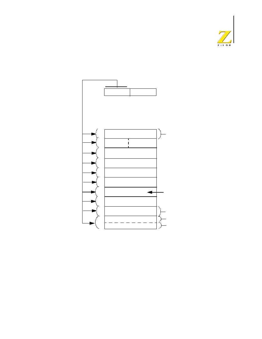
Program Memory.
The Program Memory addresses up to 4 KB of internal memory.
The first 12 bytes of program memory are reserved for the interrupt vectors.
These locations contain six 16-bit vectors that correspond to the six available

PS015601-1003
Z87C33
CMOS Z8" MCU Consumer Controller Processor
12
interrupts. Address 12 to address
4095
consists of on-chip mask-programmed
ROM.
The 4 KB program memory is mask programmable. A ROM protect feature pre-
vents dumping of the ROM contents by inhibiting execution of LDC, LDCI, LDE,
and LDEI instructions to program memory in external program mode. ROM look-
up tables can be used with this feature. The ROM Protect option is mask-pro-
grammable, to be selected by the customer when the ROM code is submitted.
See Figure 7.
Figure 7.Program Memory Map
ROM Protect.
ROM PROTECT provides an additional security function. When the
ROM PROTECT option bit is selected, and executing out of Internal Program
12
11
10
9
8
7
6
5
4
3
2
1
0
IRQ5
IRQ5
IRQ4
IRQ4
IRQ3
IRQ3
IRQ2
IRQ2
IRQ1
IRQ1
IRQ0
IRQ0
Interrupt
Vector
(Lower Byte)
Interrupt
Vector
(Upper Byte)
65537
ROM
On-Chip
Reserved
4096
4095
Location of first Byte
of Instruction Executed
after RESET

PS015601-1003
Z87C33
CMOS Z8" MCU Consumer Controller Processor
13
Memory, instructions LDC, LDCI, LDE, and LDEI can read Internal Program Mem-
ory.
RAM Protect.
The upper portion of the RAM's address spaces
80h
to
EFh
(exclud-
ing the control registers) can be protected from writing. The RAM Protect option
bit can be selected when the device is programmed. After the mask option is
selected, the user activates this feature from the internal ROM code to turn off/on
the RAM Protect by loading either a 0 or a 1 into the IMR register, bit D6. A 1 in bit
D6 enables the RAM Protect option.
Working Register File.
The Z8 standard register file (Bank 0) contains 3 I/O port
registers, 237 general-purpose registers, and 15 control and status registers.
Expanded register file Bank
Fh
contains 4 system-configuration registers. The
working registers are accessed directly or indirectly via an 8-bit address field. As a
result, a short 4-bit register address can use the Register Pointer (Table 5 and
Figure 9). In the 4-bit mode, the working register file is divided into 16 working reg-
ister groups, each occupying 16 continuous locations. The Register Pointer
addresses the starting location of the active working register group.
Throughout this document, Bank 0 is referred to as the Z8 Standard Register File.
Expanded Register File (ERF).
The Z8 register file is expanded to allow for addi-
tional system control registers, and for mapping of additional peripheral devices,
along with the I/O ports, into the register address area. The Z8 register address
space 0 through 255 is implemented as 16 groups of 16 registers per bank (Fig-
ures 8 and 9 ). There are 16 banks known as the Expanded Register File (ERF).
Bits 7≠4 of register RP select the Working Register Group. Bits 3≠0 of register RP
select the Expanded Register File Bank. Four system configuration registers
reside in the Expanded Register File at Bank
Fh
--PCON, SMR, SMR2, and
WDTMR. The remainder of the Expanded Register is not physically implemented,
and is open for future expansion.
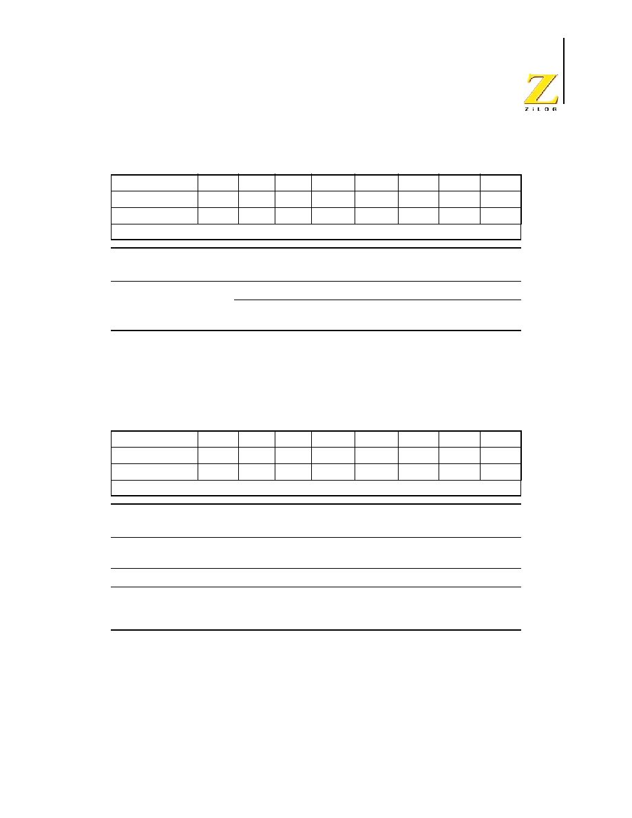
Table 4. Register Pointer Register--RP FDh/R253 Bank 0h: READ/WRITE
Bit
D7
D6
D5
D4
D3
D2
D1
D0
R/W
R/W
R/W
R/W
R/W
R/W
R/W
R/W
R/W
Reset
0
0
0
0
0
0
0
0
Note: R = Read, W = Write, X = Indeterminate.
Bit
Position
Bit
Field
R/W
Reset
State Description
D7≠D4
Working Registers
R/W
0
Working Register Group
Pointer
D3≠D0
ERF
R/W
0
Expanded Register File
PS015601-1003
Z87C33
CMOS Z8" MCU Consumer Controller Processor
14
Figure 8.Register Pointer--Detail
General-Purpose Registers (GPR).
General-purpose registers are undefined after
the device is powered up. These registers keep the most recent value after any
RESET, as long as the RESET occurs in the V
CC
voltage-specified operating
range. General-purpose registers are not guaranteed to keep their most recent
state from a Low-Voltage Protection
(V
LV
) RESET if V
CC
drops below 1.8V.
This upper nibble of the register file address
R15 to R0
FF
provided by the register pointer specifies
R253
(Register Pointer)
r7 r6 r5 r4
r3 r2 r1 r0
the active working-register group.
The lower nibble
of the register
file addresses
provided by the
instruction points
to the specified
register.
Specified Working
Register Group
Register Group 1
Register Group 0
I/O Ports
R15 to R0
R15 to R4*
R3 to R0*
7F
70
6F
60
5F
50
4F
40
3F
30
2F
20
1F
10
0F
00
* Expanded Register File Bank 0 is
selected in this figure by handling bits
D3 to D0 as "0" in Register R253 (RP).
EF
80
Register Group Fh
F0

PS015601-1003
Z87C33
CMOS Z8" MCU Consumer Controller Processor
15
Register
E0h-EFh
is only accessed via working register and
indirect addressing modes.
Stack Pointer.
The internal register file is used for the stack. An 8-bit Stack Pointer
(SPL) is used for the internal stack that resides within the 236 general-purpose
registers. Stack Pointer High (SPH) is used as a general-purpose register.
SPH and SPL are set to
00h
after any RESET or Stop-Mode
Recovery.
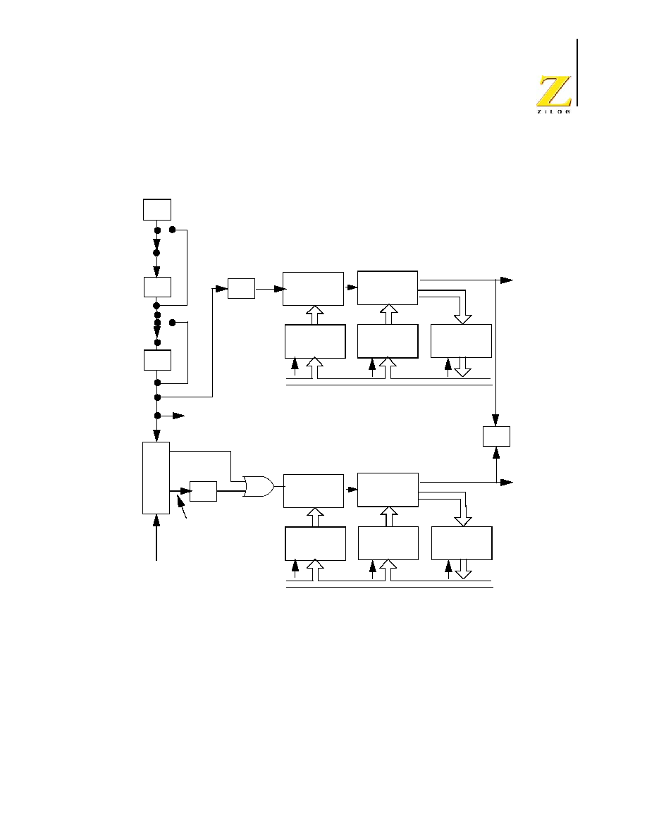
Counter/Timers.
There are two 8-bit programmable counter/timers (T0≠T1), each
driven by its own 6-bit programmable prescaler. The T1 prescaler is driven by
internal or external clock sources; however, the T0 prescaler is driven by the inter-
nal clock only (Figure 10).
The 6-bit prescalers can divide the input frequency of the clock source by any
integer number from 1 to 64. Each prescaler drives its counter, which decrements
the value (1 to 256) that is loaded into the counter. When the counter reaches the
end of the count, a timer interrupt request, IRQ4 (T0) or IRQ5 (T1), is generated.
The counters are programmed to START, STOP, restart to CONTINUE, or restart
from the initial value. The counters can also be programmed to STOP upon reach-
ing 0 (SINGLE-PASS mode) or to automatically reload the initial value and con-
tinue counting (MODULO≠N CONTINUOUS mode).
The counters, but not the prescalers, are read at any time without disturbing their
value or count mode. The clock source for T1 is user-definable and is either the
internal microprocessor clock divide-by-four, or an external signal input through
Port 3. The Timer Mode Register configures the external timer input (P31) as an
external clock, a trigger input that is retriggerable or nonretriggerable, or as a gate
input for the internal clock. The counter/timers are cascaded by connecting the T0
output to the input of T1. T
IN
mode is enabled by setting PRE1 bit D1 to 0.
Note:
Note:

PS015601-1003
Z87C33
CMOS Z8" MCU Consumer Controller Processor
16
Figure 9.Expanded Register File Architecture
REGISTER POINTER
7 6 5 4 3 2 1 0
RESET CONDITION
7 6 5 4 3 2 1 0
RESET CONDITION
Expanded Register Bank (Fh)
Working Register Group 0
Working Register
Group Pointer
Z8 Working Register File
Expanded Register
File Pointer
0Fh
00h
FF
FE
FD
FC
FB
FA
F9
F8
F5
F4
F3
F2
F1
F0
(F) 0F*
(F) 0E
(F) 0D
*
(F) 0C
(F) 0A
(F) 09
(F) 08
(F) 07
(F) 06
(F) 05
(F) 04
(F) 03
(F) 02
(F) 01
(F) 00*
WDTMR
Reserved
SMR2
Reserved
SMR
Reserved
Reserved
Reserved
Reserved
Reserved
Reserved
Reserved
Reserved
Reserved
Reserved
PCON
X
X
0
U
X
X
0
U
X
X
1
U
0
X
0
U
1
X
0
U
1
X
0
U
0
0
0
U
1
0
0
U
SPL
SPH
RP
FLAGS
IMR
IRQ
IPR
P01M
P3M
P2M
PRE0
T0
PRE1
T1
TMR
Reserved
0
0
0
X
0
0
X
0
0
1
X
X
X
X
0
0
0
0
X
X
0
X
1
0
1
X
X
X
X
0
0
0
0
X
X
0
X
0
0
1
X
X
X
X
0
0
0
0
X
X
0
X
0
0
1
X
X
X
X
0
0
0
0
X
X
0
X
1
0
1
X
X
X
X
0
0
0
0
X
X
0
X
1
0
1
X
X
X
X
0
0
0
0
X
X
0
X
0
0
1
X
X
0
X
0
0
0
0
X
X
0
X
1
0
1
0
X
0
X
0
70h
Notes
X - Indeterminate
* - Is not reset via Stop-Mode Recovery
** - Is not reset via Stop-Mode Recovery, except for bit D0
(F) 0B**
Expanded Register Bank 0h
Working Register Group F
F7*
F6*
FFh
F0h
PS015601-1003
Z87C33
CMOS Z8" MCU Consumer Controller Processor
17
Figure 10.Counter/Timer Block Diagram
Interrupts.
The Z8 features six different interrupts from six different sources.
These interrupts are maskable and prioritize. The six sources are divided as fol-
lows: four sources are claimed by Port 3 lines P33≠P30, and two are claimed by
counter/timers (Interrupt Types, Sources, and Vectors). The Interrupt Mask Regis-
ter globally or individually enables or disables the six interrupt requests.
T1
IRQ5
Internal
Clock
Clock
Logic
External Clock
˜2
Internal Clock
Gated Clock
Triggered Clock
T
IN
P31
OSC
Current Value
Write
Write
Read
Internal Data Bus
Register
6-Bit
Down
Counter
8-Bit
Down
Counter
PRE1
Initial Value
Register
T1
Initial Value
Register
˜4
T0
IRQ4
Current Value
Write
Read
Internal Data Bus
Register
6-Bit
Down
Counter
8-Bit
Down
Counter
PRE0
Initial Value
Register
T0
Initial Value
Register
Write
˜2
T
OUT
P36
˜4
D1 SMR
D0 SMR
16

PS015601-1003
Z87C33
CMOS Z8" MCU Consumer Controller Processor
18
Figure 11.Interrupt Block Diagram
Table 5. Interrupt Types, Sources, and Vectors
Name
Source
Vector Location
Comments
IRQ0
IRQ0
0,1
External (P32), Rising and Falling Edges
Triggered
IRQ1,
IRQ1
2,3
External (P33), Falling Edge Triggered
IRQ2
IRQ2, T
IN
4,5
External (P31), Rising and Falling Edges
Triggered
IRQ3
IRQ3
6,7
External (P30), Falling Edge Triggered
IRQ4
T0
8,9
Internal
IRQ5
T1
10,11
Internal
IRQ
IMR
IPR
6
Priority
Logic
Interrupt
Request
Global
Interrupt
Enable
Vector Select
Interrupt
Edge
Select
IRQ0 IRQ2
IRQ
(D6, D7)
IRQ1,3,4,5

PS015601-1003
Z87C33
CMOS Z8" MCU Consumer Controller Processor
19
When more than one interrupt is pending, priorities are resolved by a programma-
ble priority encoder that is controlled by the Interrupt Priority register. An interrupt
machine cycle activates when an interrupt request is granted. This action disables
all subsequent interrupts, saves the Program Counter and Status Flags, and then
branches to the program memory vector location reserved for that interrupt.
All Z8 interrupts are vectored through locations in the program memory. This
memory location and the next byte contain the 16-bit address of the interrupt ser-
vice routine for that particular interrupt request. To accommodate polled interrupt
systems, interrupt inputs are masked and the Interrupt Request register is polled
to determine which of the interrupt requests require service.
When in ANALOG mode, an interrupt resulting from AN1 maps to IRQ2, and an
interrupt from AN2 maps to IRQ0. Interrupts IRQ2 and IRQ0 may be rising, falling,
or both edge-triggered, and are programmed in the IRQ register. The software
polls to identify the state of the pin. When in ANALOG mode, IRQ1 is generated
by the Stop-Mode Recovery source selected by SMR Register bits D4, D3, D2, or
SMR2 D1 or D0.
Programming bits for the Interrupt Edge Select are located in the IRQ register, bits
D7 and D6. The configuration is indicated in Table 7.
Clock.
The Z8 on-chip oscillator features a high-gain, parallel-resonant amplifier
for connection to a crystal, LC, RC, ceramic resonator, or any suitable external
clock source (X
IN
= INPUT, X
OUT
= OUTPUT). The crystal should be AT-cut, 4
MHz maximum, with a series resistance (RS) of less than or equal to 100
when
oscillating from 1MHz to 4MHz.
The crystal should be connected across XTAL1 and XTAL2 using the vendor's
recommended capacitor values from each pin directly to the device Ground pin to
reduce ground-noise injection into the oscillator. The RC oscillator option is mask-
Table 6. IRQ Register*
IRQ
Interrupt Edge
D7
D6
P31
P32
0
0
F
F
1
F
R
1
0
R
F
1
1
R/F
R/F
Notes:
F = Falling Edge
R = Rising Edge

PS015601-1003
Z87C33
CMOS Z8" MCU Consumer Controller Processor
20
programmable and is selectable by the customer at the time the ROM code is
submitted.
The
RC
option is available up to 4MHz. The
RC
oscillator
configuration must be an external resistor connected from
X
IN
to
X
OUT
, with a frequency-setting capacitor from
X
IN
to Ground
(Figure 12).
For better noise immunity, the capacitors should be tied directly
to the device Ground pin (
V
SS
).
Figure 12.Oscillator Configuration
Power-On Reset (POR).
A timer circuit clocked by a dedicated on-board RC oscilla-
tor is used for the Power-On Reset (POR) timer function. The POR time allows
V
CC
and the oscillator circuit to stabilize before instruction execution begins.
The POR timer circuit is a one-shot timer triggered by one of three conditions:
1. Power fail to Power OK status.
2. Stop-Mode Recovery (if D5 of SMR = 1).
3. WDT time-out.
The POR time is specified as TPOR. Bit 5 of the Stop-Mode Register determines
whether the POR timer is bypassed after Stop-Mode Recovery (typical for external
clock, RC/LC oscillators).
HALT.
HALT turns off the internal CPU clock, but not the CRYSTAL oscillation.
The counter/timers, analog comparators, and external interrupts IRQ0, IRQ1,
IRQ2, and IRQ3 remain active. The devices are recovered by interrupts and are
either externally or internally generated. This also includes WDT time-out Reset
Notes:
C1
**
XTAL1
XTAL2
LC Clock
C2
V
SS
**
C1
**
C2
V
SS
**
External Clock
RC Clock
XTAL1
XTAL2
XTAL1
XTAL2
XTAL1
XTAL2
L
R
V
SS
**
C
Ceramic
Resonator
or Crystal
C1, C2 = 47
µfd*
f = 4MHz
C1, C2 = 22 pf
L =130
µH*
f = 3 MHz*
*Preliminary value, including pin parasitics
** Device Ground Pin
@5V V
CC
(TYP)
C1 = 44pF*
R = 4K ohm
f = 3 MHz*

PS015601-1003
Z87C33
CMOS Z8" MCU Consumer Controller Processor
21
and V
LV
Reset. An interrupt request must be enabled and executed to exit HALT
mode. After the interrupt service routine, the program continues from the instruc-
tion after the HALT.
In order to enter STOP (or HALT) mode, it is necessary to first flush the instruction
pipeline to avoid suspending execution in mid-instruction. The user must execute
a NOP (Op Code =
FFh
) immediately before the appropriate sleep instruction. For
example:
or
STOP.
This instruction turns off the internal clock and external crystal oscillation.
The STOP instruction also reduces the standby current to 10 µA or less. The ana-
log comparators are automatically powered down in STOP-Mode. STOP mode is
terminated either by WDT time-out, POR, Stop-Mode Recovery, or any Reset. As
a result, the processor restarts the application program at address
000Ch
. A WDT
time-out in STOP mode affects all registers the same as if a Stop-Mode Recovery
occurred via a selected Stop-Mode Recovery source except that the POR delay is
enabled even if the delay is selected for disable.
If a permanent
WDT
is selected, the
WDT
runs in all modes and
cannot be stopped or disabled if the onboard
RC
oscillator is
selected to drive the
WDT
.
Port Configuration Register (PCON).
The PCON register configures the ports indi-
vidually; comparator output on Port 3, open-drain on Port 0 and Port 1, low EMI on
Ports 0, 1, 2, and 3, and low-EMI oscillator. The PCON register is located in the
expanded register file at Bank F, location
00h
(Table 8).
FF
NOP
; clear the pipeline
6F
STOP ; enter STOP mode
FF
NOP
; clear the pipeline
7F
HALT ; enter HALT mode
Note:

PS015601-1003
Z87C33
CMOS Z8" MCU Consumer Controller Processor
22
Comparator Output Port 3 (D0).
Bit 0 controls the comparator use in Port 3. A 1 in
this location brings the comparator outputs to P34 and P37, and a 0 releases the
Port to its standard I/O configuration. The default value is 0.
Port 0 Open-Drain (D2).
Port 0 is configured as an open-drain by resetting this bit
(D2 = 0) or configured as push-pull active by setting this bit (D2 = 1). The default
value is 1.
Low-EMI Port 0 (D3).
Port 0 is configured as a low-EMI port by resetting this bit (D3
= 0) or configured as a Standard Port by setting this bit (D3 = 1). The default value
is 1.
Table 7. Port Configuration Register--PCON 00h/R0 Bank Fh: WRITE ONLY
Bit
D7
D6
D5
D4
D3
D2
D1
D0
R/W
W
W
W
W
W
W
W
W
Reset
1
1
1
1
1
1
1
0
Note: R = Read, W = Write, X = Indeterminate.
Bit
Position
Bit
Field
R/W
Reset
State Description
D7
Oscillator
W
1
Low-EMI Oscillator
0: Low EMI
1: Standard
D6
Port 3 I/O
W
1
Port 3
0: Low EMI
1: Standard
D5
Port 2 I/O
W
1
Port 2
0: Low EMI
1: Standard
D4
Reserved
W
1
Reserved*
1: Must be "1"
D3
Port 0 I/O
W
1
Port 0*
0: Low EMI
1: Standard
D2
Port 0 I/O
W
1
Port 0
0: Open-Drain
1: Push-Pull Active
D1
Reserved
W
1
Reserved*
1: Must be "1"
D0
Port 3
W
0
Port 3 Comparator Output
0: P34, P37 Standard Output
1: P34, P37 Comparator Output

PS015601-1003
Z87C33
CMOS Z8" MCU Consumer Controller Processor
23
Low-EMI Port 2 (D5).
Port 2 is configured as a low-EMI port by resetting this bit (D5
= 0) or configured as a Standard Port by setting this bit (D5 = 1). The default value
is 1.
Low-EMI Port 3 (D6).
Port 3 is configured as a low-EMI port by resetting this bit (D6
= 0) or configured as a Standard Port by setting this bit (D6 = 1). The default value
is 1.
Low-EMI OSC (D7).
This bit of the PCON register controls the low-EMI noise oscil-
lator. A 1 in this location configures the oscillator, DS, AS and R/W with standard
drive, while a 0 configures the oscillator, DS, AS and R/W with low noise drive.
LOW-EMI mode reduces the drive of the oscillator (OSC). The default value is 1.
Maximum external clock frequency of 4 MHz when running in
LOW-EMI OSCILLATOR mode.
Low-EMI Emission.
The Z8 is programmed to operate in a low-EMI emission mode
in the PCON register. The oscillator and all I/O ports is programmed as LOW-EMI
EMISSION mode independently. Use of this feature results in:
∑
The pre-drivers slew rate reduced to 10 ns (typical)
∑
Low-EMI output drivers exhibit resistance of 200
(typical)
∑
Low-EMI Oscillator
∑
Internal SCLK = X
IN
operation limited to a maximum of 4 MHz≠250 ns cycle time,
when LOW EMI OSCILLATOR is selected and system clock (SMR Register Bit
D1 = 1)
Stop-Mode Recovery Registers (SMR1 and SMR2).
These registers select the clock
divide value and determine the mode of Stop-Mode Recovery (Tables 8 and 11).
All bits are WRITE ONLY, except bit 7 of SMR1, which is READ ONLY. SMR1 bit 7
is a flag bit that is set by hardware on a Stop-Mode Recovery condition and reset
by a power-on cycle. For SMR1, bit 6 controls whether a Low level or a High level
is required from the recovery source. Bit 5 controls the reset delay after Stop-
Mode Recovery. Bits 2, 3, and 4 of the SMR1 register specify the source of the
Stop-Mode Recovery signal. Bits 0 and 1 determine the time-out period of the
WDT. The SMR registers are located in Bank F of the Expanded Register File at
addresses
0Bh
and
0Dh
, respectively.
For SMR2, bits 7 to 2 are reserved. Bits 1 and 0 of the SMR2 register specify the
source of the Stop-Mode Recovery signal.
Table 8. Stop-Mode Recovery Register 1--SMR1 0Bh/R11 Bank Fh: WRITE ONLY, except Bit D7,
which is READ ONLY
Bit
D7
D6
D5
D4
D3
D2
D1
D0
R/W
R
W
W
W
W
W
W
W
Note:

PS015601-1003
Z87C33
CMOS Z8" MCU Consumer Controller Processor
24
SCLK & TCLK Divide-by-16 Select (D0).
Bit D0 of the SMR controls a divide-by-16
prescaler of SCLK & TCLK. The purpose of this control is to selectively reduce
device power consumption during normal processor execution (SCLK control)
and/or HALT mode (where TCLK sources counter/timers and interrupt logic). This
bit is reset to D0 = 0 after a Stop-Mode Recovery.
Reset
0
0
1
0
0
0
0
0
Note: R = Read, W = Write, X = Indeterminate.
Bit
Position
Bit
Field
R/W
Reset
State Description
D7
STP
R
0
Stop Flag
0: POR
1: Stop-Mode Recovery
D6
SMR
W
0
Stop-Mode Recovery Level
0: Low
1: High
D5
STPDLY
W
1
Stop Delay
0: Off
1: On
D4≠D2
SMRSRC
W
000
Stop-Mode Recovery Source
1
000: POR only and/or external RESET
001: P30
010: P31
011: P32
100: P33
101: P27
110: P2 NOR 0≠3
111: P2 NOR 0≠7
D1
EXTCLK
W
0
External Clock Divide-by-2
0: SCLK & TCLK = XTAL ˜ 2
1: SCLK & TCLK = XTAL
D0
CLK
W
0
SCLK & TCLK Divide-by-16
0: Off
2
1: On
Notes:
1. Do not use in conjunction with SMR2 Source.
2. Cleared by RESET and SMR.
Table 8. Stop-Mode Recovery Register 1--SMR1 0Bh/R11 Bank Fh: WRITE ONLY, except Bit D7,
which is READ ONLY

PS015601-1003
Z87C33
CMOS Z8" MCU Consumer Controller Processor
25
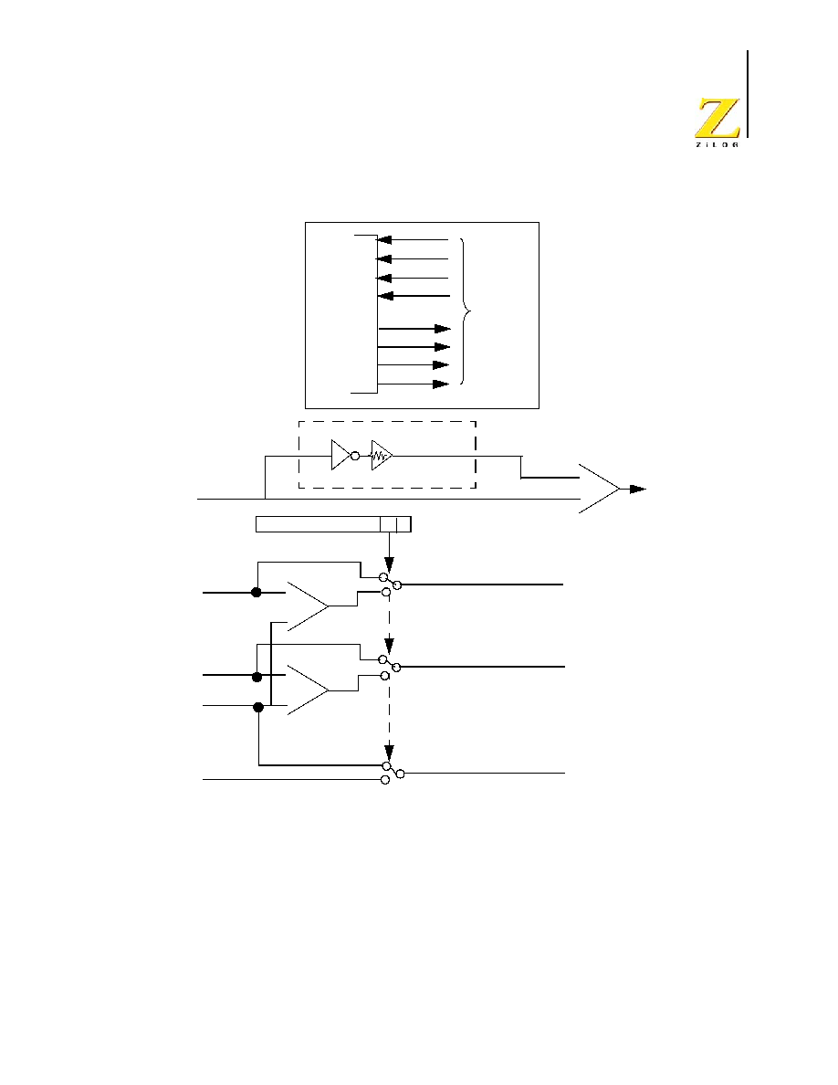
External Clock Divide-by-Two (D1).
This bit can eliminate the oscillator divide-by-
two circuitry. When this bit is 0, the system clock (SCLK) and timer clock (TCLK)
are equal to the external clock frequency divided by 2. The SCLK is equal to the
external clock frequency when this bit is set (D1 = 1). Using this bit together with
D7 of PCON further helps lower EMI (that is, D7 (PCON) = 0, D1 (SMR) = 1). The
default setting is 0. Maximum external clock frequency is 4 MHz when SMR bit D1
= 1 where SCLK & TCLK = X
IN
.
Stop-Mode Recovery Source (D2, D3, and D4).
These three bits of the SMR specify
the wake-up source of the Stop-Mode Recovery (Figure and Stop-Mode Recov-
ery Source). When the Stop-Mode Recovery Sources are selected in this register,
then SMR2 register bits D0,D1 must be set to 0.
If the Port 2 pin is configured as an output, this output level is
read by the
SMR
circuitry.
Figure 13.Stop-Mode Recovery Source
Note:
P30
P31
P32
P33
P27
SMR
M
U
X
P33 From Pads
Digital/Analog Mode
Select (P3M)
Stop-Mode Recovery Edge
Select (SMR)
To P33
Data Latch
and IRQ1
SMR2
P20
P23
P20
P27
To POR
RESET
V
DD
V
DD
P20
P27
P20
P23
SMR2
SMR2
SMR
SMR
SMR
SMR
D1 D0
0 0
D1 D0
0 1
D1 D0
1 0
D4 D3 D2
0 0 0
D4 D3 D2
0 0 0
0 1 0
0 1 1
D4 D3 D2
1 0 0
D4 D3 D2
1 0 1
D4 D3 D2
1 1 0
D4 D3 D2
1 1 1
SMR
PS015601-1003
Z87C33
CMOS Z8" MCU Consumer Controller Processor
26
Stop-Mode Recovery Delay Select (D5).
This bit, if High, enables the T
POR
RESET
delay after Stop-Mode Recovery. The default configuration of this bit is 1. If the
fast wake up (no delay) is selected, the Stop-Mode Recovery source must be kept
active for at least 5 T
P
C. The clock source must be RC/LC/external clock driven.
Stop-Mode Recovery Edge Select (D6).
A 1 in this bit position indicates that a high
level on any one of the recovery sources wakes the Z8 from STOP mode. A 0 indi-
cates low-level recovery. The default is 0 on POR (Table 11). This bit is used for
either SMR or SMR2.
Cold or Warm Start (D7).
This bit is set by the device upon entering STOP mode. A
0 in this bit (cold) indicates that the device resets by POR/WDT RESET. A 1 in this
bit (warm) indicates that the device awakens by a Stop-Mode Recovery source.
If the Port 2 pin is configured as an output, this output level is
read by the
SMR2
circuitry.
Stop-Mode Recovery Register 2 (SMR2).
This register contains additional Stop-
Mode Recovery sources. When the Stop-Mode Recovery sources are selected in
this register then SMR register bits D2, D3, and D4 must be 0.
Table 9. Stop-Mode Recovery Source
SMR[4≠2]
D4
D3
D2
Operation/Description of Action
0
0
0
POR and/or external reset recovery
0
0
1
P30 transition
0
1
0
P31 transition (not in ANALOG mode)
0
1
1
P32 transition (not in ANALOG mode)
1
0
0
P33 transition (not in ANALOG mode)
1
0
1
P27 transition
1
1
0
Logical NOR of P20 through P23
1
1
1
Logical NOR of P20 through P27
Table 10. Stop-Mode Recovery Register 2
SMR1≠0
D1
D0
Operation/Description of Action
0
0
POR and/or external reset recovery
Note:

PS015601-1003
Z87C33
CMOS Z8" MCU Consumer Controller Processor
27
Watch-Dog Timer Mode Register (WDTMR).
The WDT is a retriggerable one-shot
timer that resets the Z8 if it reaches its terminal count. The WDT is initially enabled
by executing the WDT instruction and refreshed on subsequent executions of the
WDT instruction. The WDT circuit is driven by an onboard RC oscillator or exter-
nal oscillator from the X
IN
pin. The POR clock source is selected with bit 4 of the
WDT register (Table 15).
WDT instruction affects the Z (Zero), S (Sign), and V (Overflow) flags. The
WDTMR must be written to within the first 60 internal system clocks. After that, the
WDTMR is WRITE-protected.
WDT
time-out while in
STOP
mode does not reset SMR, PCON,
WDTMR, P2M, P3M, Ports 2 & 3 Data Registers, but the
POR
delay counter is still enabled even though the
SMR
stop delay is
disabled.
0
1
Logical AND of P20 through P23
1
0
Logical AND of P20 through P27
Table 11. Stop-Mode Recovery Register 2--SMR2 0Dh/R13 Bank Fh: WRITE ONLY
Bit
D7
D6
D5
D4
D3
D2
D1
D0
R/W
W
W
W
W
W
W
W
W
Reset
X
X
X
X
X
X
0
0
Note: R = Read, W = Write, X = Indeterminate.
Bit/
Field
Bit
Position
R/W
Reset
State Description
D7≠D2 Reserved
W
X
Reserved--must be 0
D1≠D0 STOP Mode
W
00
Stop-Mode Recovery Source 2*
00: POR only
01: AND P20, P21, P22, P23
10: AND P20, P21, P22, P23, P24, P25,
P26, P27
11: Reserved
Note: *Do not use in conjunction with SMR Source.
Table 10. Stop-Mode Recovery Register 2
SMR1≠0
D1
D0
Operation/Description of Action
Note:

PS015601-1003
Z87C33
CMOS Z8" MCU Consumer Controller Processor
28
WDT Time Select (D0,D1).
Selects the WDT time period and is configured as indi-
cated in Table 14.
WDTMR During HALT (D2).
This bit determines whether or not the WDT is active
during HALT mode. A 1 indicates active during HALT. The default is 1.
Table 12. Watch-Dog Timer Mode Register--WDTMR 0Fh/R15: WRITE ONLY
Bit
D7
D6
D5
D4
D3
D2
D1
D0
R/W
W
W
W
W
W
W
W
W
Reset
X
X
X
0
1
1
0
1
Note: R = Read, W = Write, X = Indeterminate.
Bit/
Field
Bit
Position
R/W
Reset
State Description
D7≠D5 Reserved
W
X
Reserved--must be 0
D4
X
IN
W
0
XIN/INT RC Select for WDT
0: On-Board RC
1: X
IN
D3
WDT
W
1
WDT During STOP
D2
WDT
W
1
WDT During HALT
D1≠D0 WDT Tap
W
01
WDT Tap Int RC OSC
System Clock
00:
3.5 ms
128 SCLK
01:
7.0 ms
256 SCLK
10:
14.0 ms
512 SCLK
11:
56.0 ms
2048 SCLK
Note: Not used in conjunction with SMR Source.
Table 13. WDT Time Select
D1
D0
Timeout of Internal RC OSC
Timeout of System Clock
0
0
3.5 ms min
128 SCLK
0
1
7 ms min
256 SCLK
1
0
14 ms min
512 SCLK
1
1
56 ms min
2048 SCLK
Note: SCLK = system bus clock cycle. The default on RESET is 7 ms. Values provided are for VCC
= 5.0V.

PS015601-1003
Z87C33
CMOS Z8" MCU Consumer Controller Processor
29
WDTMR During STOP (D3).
This bit determines whether or not the WDT is active
during STOP mode. Because the X
IN
clock is stopped during STOP mode, the on-
board RC must be selected as the clock source to the POR counter. A 1 indicates
active during STOP. The default is 1.
If the permanent
WDT
programming option is selected, the
WDT
runs in all modes and cannot be stopped or disabled if the on
board RC oscillator is selected as the clock source for
WDT
.
Clock Source for WDT (D4).
This bit determines which oscillator source is used to
clock the internal POR and WDT counter chain. If the bit is a 1, the internal RC
oscillator is bypassed and the POR and WDT clock source is driven from the
external pin, X
IN
. The default configuration of this bit is 0 which selects the internal
RC oscillator.
WDTMR Register Accessibility.
The WDTMR register is accessible only during the
first 64 internal system clock cycles from the execution of the first instruction after
Power-On Reset, Watch-Dog Reset, or Stop-Mode Recovery. After this point, the
register cannot be modified by any means, intentional or otherwise. The WDTMR
cannot be read and is located in Bank
Fh
of the Expanded Register File at
address location
0Fh
(Figure 14).
The
WDT
is permanently enabled (automatically enabled after
RESET
) through a programmable option. The option is selected
when the device is programmed. In this mode,
WDT
is always
activated when the device comes out of
RESET
. Execution of
the
WDT
instruction serves to refresh the
WDT
time-out period.
WDT
operation in the
HALT
and
STOP
modes is controlled by
WDTMR
programming. If this option is not selected when the
device is programmed, the
WDT
must be activated by the user
through the
WDT
instruction and is always disabled by any reset
to the device.
Note:
Note:
PS015601-1003
Z87C33
CMOS Z8" MCU Consumer Controller Processor
30
Figure 14.Resets and Watch-Dog Timer Example
Voltage Comparator
Low-Voltage Protection.
An onboard Voltage Comparator checks that V
CC
is at the
required level to ensure correct operation of the device. RESET is globally driven
if V
CC
is below the specified voltage (Low-Voltage Protection). The minimum oper-
ating voltage varies with the temperature and operating frequency, while the Low-
Voltage Protection (V
LV
) varies with temperature only.
The Low-Voltage Protection trip voltage (V
LV
) is less than 3V and more than 1.4V
under the following conditions.
At 25∫C, the device functions normally at or above 3.0V. Below 3.0V, the device
functions normally until the Low-Voltage Protection trip point (V
LV
) is reached for
the temperatures and operating frequencies in Table 15. The device is guaranteed
to function normally at supply voltages above the Low-Voltage Protection trip
Clear
CLK
18 Clock RESET
Generator
RESET
4 Clock
Filter
Reset
Intern
RESET
I
hhh
bbbmc
cbcbb
I
Internal
RESET
M
U
X
7ms POR 3.5ms 7ms 14ms 56ms
CK
WDT/POR Counter Chain
CLK
WDT TAP SELECT
XTAL
WDT Select (WDTMR)
Clock Source Select (WDTMR)
Internal
RC OSC
+
-
V
DD
V
LV
V
LV
Operating
Voltage Det.
WDT
WWW
WDT
From Stop Mode Recovery Source
Stop Delay Select (SMR)

PS015601-1003
Z87C33
CMOS Z8" MCU Consumer Controller Processor
31
point. The actual Low-Voltage Protection trip point is a function of temperature
and process parameters (Figure 15).
Figure 15.Typical Low-Voltage Protection vs. Temperature
The internal clock frequency relationship to the
CRYSTAL
clock
is dependent on
SMR
Bit
0 1
setting.
Table 14. Maximum (V
LV
) Conditions:
Internal Clock Frequency equal or less than 4 MHz
V
CC
3.80
(Volts)
3.60
3.40
3.20
3.00
2.80
2.60
2.40
-60∞ -40∞
-20∞
+20∞
0∞
+40∞ +60∞
+80∞
Temp
+100∞ +120∞ +140∞
V
LV
(Typical)
Note:

PS015601-1003
Z87C33
CMOS Z8" MCU Consumer Controller Processor
32
Control Registers
The Z87C33 offers 2 banks of registers, as detailed in the following pages.
Expanded Register File, Bank 0h
Bank
0h
of the Expanded Register File contains 15 Control registers that perform
the Timer, Prescaler, Port, Interrupt, Flag, and Pointer functions, as shown in
Tables 16 through 30. Table 15 lists the reset states of all 15 Bank
0h
Control reg-
isters.
Timer Mode Register
The Timer Mode Register, TMR, controls timing and counter functions. READ/
WRITE and reset states for bits D7≠D0 are listed in Table 16.
Table 15. Expanded Register File Registers--Reset States
D7
D6
D5
D4
D3
D2
D1
D0
F0h
Reserved
F1h
TMR
0
0
0
0
0
0
0
0
F2h
T1
X
X
X
X
X
X
X
X
F3h
PRE1
X
X
X
X
X
X
0
0
F4h
T0
X
X
X
X
X
X
X
X
F5h
PRE0
X
X
X
X
X
X
X
0
F6h
P2M*
1
1
1
1
1
1
1
1
F7h
P3M*
0
0
0
0
0
0
0
0
F8h
P01M
0
1
0
0
1
1
0
1
F9h
IPR
X
X
X
X
X
X
X
X
FAh
IRQ
0
0
0
0
0
0
0
0
FBh
IMR
0
X
X
X
X
X
X
X
FCh
FLAGS
X
X
X
X
X
X
X
X
FDh
RP
0
0
0
0
0
0
0
0
FEh
SPH
0
0
0
0
0
0
0
0
FFh
SPL
0
0
0
0
0
0
0
0
Note: *Not reset with a Stop-Mode Recovery.

PS015601-1003
Z87C33
CMOS Z8" MCU Consumer Controller Processor
33
Counter/Timer 1 Register
The Counter/Timer 1 Register, T1, controls timing and counter functions. READ/
WRITE and reset states for bits D7≠D0 are listed in Table 17.
Table 16. Timer Mode Register--TMR F1h/R241 Bank 0h: READ/WRITE
Bit
D7
D6
D5
D4
D3
D2
D1
D0
R/W
R/W
R/W
R/W
R/W
R/W
R/W
R/W
R/W
Reset State
0
0
0
0
0
0
0
0
Note: R = Read, W = Write.
Bit
Position
Bit
Field
R/W
Reset
State Description
D7≠D6
T
OUT
Mode
R/W
00
T
OUT
Mode
00: Off
01: T0 Output
10: T1 Output
11: Internal Clock Output
D5≠D4
T
IN
Mode
R/W
00
T
IN
Mode
00: External Clock Input
01: Gate Input
10: Trigger Input (nonretriggerable)
11: Trigger Input (retriggerable)
D3
T1 Count
R/W
0
T1 Count
0: Disable
1: Enable
D2
T1
R/W
0
T1
0: No Function
1: Load T1
D1
T0 Count
R/W
0
T0 Count
0: Disable
1: Enable
D0
T0
R/W
0
T0
0: No Function
1: Load T0
Table 17. Counter/Timer 1 Register--T1 F2h/R242 Bank 0h: READ/WRITE
Bit
D7
D6
D5
D4
D3
D2
D1
D0
R/W
R/W
R/W
R/W
R/W
R/W
R/W
R/W
R/W

PS015601-1003
Z87C33
CMOS Z8" MCU Consumer Controller Processor
34
Prescaler 1 Register
The Prescaler 1 Register, PRE1, controls clocking functions. READ/WRITE and
reset states for bits D7≠D0 are listed in Table 18.
Counter/Timer 0 Register
The Counter/Timer 0 Register, T0, controls timing and counter functions. READ/
WRITE and reset states for bits D7≠D0 are listed in Table 19.
Reset State
X
X
X
X
X
X
X
X
Note: R = Read, W = Write, X = Indeterminate.
Bit
Position
Bit
Field
R/W
Reset
State Description
D7≠D0
T1
R
X
T1 Current Value
W
X
T1 Automatic Reload Value
Range = 1≠256 decimal; 01h≠00h
Table 18. Prescaler 1 Register--PRE1 F3h/R243 Bank 0h: WRITE ONLY
Bit
D7
D6
D5
D4
D3
D2
D1
D0
R/W
W
W
W
W
W
W
W
W
Reset State
X
X
X
X
X
X
0
0
Note: W = Write, X = Indeterminate.
Bit
Position
Bit
Field
R/W
Reset
State Description
D7≠D2
Prescaler
W
X
Prescaler Modulo
Range = 1≠64 decimal; 01h≠00h
D1
Clock
W
0
Clock Source
0: T1 External Timing Input (T
IN
) Mode
1: T1 Internal
D0
Count
W
0
Count Mode
0: T1 Single Pass
1: T1 Modulo N
Table 17. Counter/Timer 1 Register--T1 F2h/R242 Bank 0h: READ/WRITE
PS015601-1003
Z87C33
CMOS Z8" MCU Consumer Controller Processor
35
Prescaler 0 Register
The Prescaler 0 Register PRE0 controls clocking functions. WRITE and reset
states for bits D7≠D0 are listed in Table 20.
Table 19. Counter/Timer 0 Register--T0 F4h/R244 Bank 0h: READ/WRITE
Bit
D7
D6
D5
D4
D3
D2
D1
D0
R/W
R/W
R/W
R/W
R/W
R/W
R/W
R/W
R/W
Reset State
X
X
X
X
X
X
X
X
Note: R = Read, W = Write, X = Indeterminate.
Bit
Position
Bit
Field
R/W
Reset
State Description
D7≠D0
T0
R
X
T0 Current Value
W
X
T0 automatic Reload Value
Range = 1≠256 decimal;
01h - 00h
Table 20. Prescaler 0 Register--PRE0 F5h/R245 Bank 0h: WRITE ONLY
Bit
D7
D6
D5
D4
D3
D2
D1
D0
R/W
W
W
W
W
W
W
W
W
Reset State
X
X
X
X
X
X
X
0
Note: W = Write, X = Indeterminate.
Bit
Position
Bit
Field
R/W
Reset
State Description
D7≠D2
Prescaler
W
X
Prescaler Modulo
Range = 1≠64 decimal; 01h≠00h
D1
Reserved
W
X
Reserved--must be 0
D0
Count
W
0
Count Mode
0: T0 Single Pass
1: T0 Modulo N
PS015601-1003
Z87C33
CMOS Z8" MCU Consumer Controller Processor
36
Port 2 Mode Register
The Port 2 Mode Register, P2M, controls Port 2 I/O functions. WRITE and reset
states for bits D7≠D0 are listed in Table 21.
Port 3 Mode Register
The Port 3 Mode Register P3M controls Port 3 I/O functions. WRITE and reset
states for bits D7≠D0 are listed in Table 22.
Table 21. Port 2 Mode Register--P2M F6h/R246 Bank 0h: WRITE ONLY
Bit
D7
D6
D5
D4
D3
D2
D1
D0
R/W
W
W
W
W
W
W
W
W
Reset State
1
1
1
1
1
1
1
1
Note: W = Write.
Bit
Position
Bit
Field
R/W
Reset
State Description
D7≠D0
P20≠P27
W
1
P20≠P27 I/O Definition
0: Defines bit as Output
1: Defines bit as Input
Table 22. Port 3 Mode Register--P3M F7h/R247 Bank 0h: WRITE ONLY
Bit
D7
D6
D5
D4
D3
D2
D1
D0
R/W
W
W
W
W
W
W
W
W
Reset State
0
0
0
0
0
0
0
0
Note: W = Write.
Bit
Position
Bit
Field
R/W
Reset
State Description
D7≠D2
Reserved
W
00
Reserved--must be 00
D1
Port 3
W
0
Port 3
0: P31, P32 DIGITAL mode
1: P31, P32 ANALOG mode
D0
Port 2
W
0
Port 2
0: Open-Drain
1: Push-Pull
PS015601-1003
Z87C33
CMOS Z8" MCU Consumer Controller Processor
37
Ports 0 and 1 Mode Register
The Ports 0 and 1 Mode Register, P01M, controls port and timing functions for
Ports 0 and 1. WRITE and reset states for bits D7≠D0 are listed in Table 23.
Interrupt Priority Register
The Interrupt Priority Register, IPR, prioritizes interrupt functions. WRITE and
reset states for bits D7≠D0 are listed in Table 24.
Table 23. Ports 0 and 1 Mode Register--P01M F8h/R248 Bank 0h: WRITE ONLY
Bit
D7
D6
D5
D4
D3
D2
D1
D0
R/W
W
W
W
W
W
W
W
W
Reset State
0
1
0
0
1
1
0
1
Note: W = Write.
Bit
Position
Bit
Field
R/W
Reset
State Description
D7
Reserved
W
0
Reserved - Must be 0
D6
P04≠P07
W
01
P04≠P07 Mode*
0: Output
1: Input
D5
Reserved
W
0
External Memory Timing
Reserved - Must be 0
D4≠D3
Reserved
W
01
P10≠P17 Mode*
00: Reserved - Must be 0
D2
Stack
W
1
Stack Selection*
0: Reserved
1: Must be "1"
D1
Reserved
W
0
Reserved - Must be 0
D0
P00≠P03
W
1
P00≠P03 Mode*
0: Output
1: Input
Table 24. Interrupt Priority Register--IPR F9h/R249 Bank 0h: WRITE ONLY
Bit
D7
D6
D5
D4
D3
D2
D1
D0
R/W
W
W
W
W
W
W
W
W
Reset State
X
X
X
X
X
X
X
X
Note: W = Write, X = Indeterminate.

PS015601-1003
Z87C33
CMOS Z8" MCU Consumer Controller Processor
38
Interrupt Request Register
The Interrupt Request Register, IRQ, controls interrupt functions. READ/WRITE
and reset states for bits D7≠D0 are listed in Table 25.
Bit Position
Bit
Field
R/W
Reset
State Description
D7≠D6
Reserved
W
XX
Reserved--must be 0
D5
IRQ3, IRQ5
W
X
IRQ3, IRQ5 Priority (Group A)
0: IRQ5 > IRQ3
1: IRQ3 > IRQ5
D4,D3,D0
Interrupt
W
XXX
Interrupt Group Priority
000: Reserved
001: C > A > B
010: A > B > C
011: A > C > B
100: B > C > A
101: C > B > A
110: B > A > C
111: Reserved
D2
IRQ0, IRQ2
W
X
IRQ0, IRQ2 Priority (Group B)
0: IRQ2 > IRQ0
1: IRQ0 > IRQ2
D1
IRQ1, IRQ4
W
X
IRQ1, IRQ4 Priority (Group C)
0: IRQ1 > IRQ4
1: IRQ4 > IRQ1
Table 25. Interrupt Request Register--IRQ FAh/R250 Bank 0h: READ/WRITE
Bit
D7
D6
D5
D4
D3
D2
D1
D0
R/W
R/W
R/W
R/W
R/W
R/W
R/W
R/W
R/W
Reset
0
0
0
0
0
0
0
0
Note: R = Read, W = Write.

PS015601-1003
Z87C33
CMOS Z8" MCU Consumer Controller Processor
39
Interrupt Mask Register
The Interrupt Mask Register, IMR, controls interrupt functions. READ/WRITE and
reset states for bits D7≠D0 are listed in Table 26.
Bit
Position
Bit
Field
R/W
Reset
State Description
D7≠D6
Interrupt
Edge
R/W
00
Interrupt Edge
00: P31
P32
01: P31
P32
10: P31
P32
11: P31
P32
D5
IRQ5
R/W
0
Interrupt
IRQ5 = T1
0: No Interrupt pending
1: Interrupt pending
D4
IRQ4
R/W
0
Interrupt
IRQ4 = T0
0: No Interrupt pending
1: Interrupt pending
D3
IRQ3
R/W
0
Interrupt
IRQ3 = P30 Input
0: No Interrupt pending
1: Interrupt pending
D2
IRQ2
R/W
0
Interrupt
IRQ2 = P31 Input
0: No Interrupt pending
1: Interrupt pending
D1
IRQ1
R/W
0
Interrupt
IRQ1 = P33 Input
0: No Interrupt pending
1: Interrupt pending
D0
IRQ0
R/W
0
Interrupt
IRQ0 = P32 Input
0: No Interrupt pending
1: Interrupt pending
Table 26. Interrupt Mask Register--IMR FBh/R251 Bank 0h: READ/WRITE
Bit
D7
D6
D5
D4
D3
D2
D1
D0
R/W
R/W
R/W
R/W
R/W
R/W
R/W
R/W
R/W

PS015601-1003
Z87C33
CMOS Z8" MCU Consumer Controller Processor
40
Flags Register
The CPU sets flags in the Flags Register, FLAGS, to allow the user to perform
tests based on differing logical states. READ/WRITE and reset states for bits D7≠
D0 are listed in Table 27.
Reset
0
X
X
X
X
X
X
X
Note: R = Read, W = Write, X = Indeterminate.
Bit
Position
Bit
Field
R/W
Reset
State Description
D7
MIE
R/W
0
Master Interrupt Enable
1: Enable interrupts
0: Disable interrupts
D6
RAM Protect
R/W
X
RAM Protect
1: Enable RAM Protect*
0: Disable RAM Protect
D5≠D0
IRQ5≠IRQ0
R/W
X
Interrupt Request
1: Enable IRQ0≠IRQ5
0: Disable IRQ0≠IRQ5
Note: * Must select RAM Protect Mask Option
Table 27. Flags Register--FLAGS FCh/R252 Bank 0h: READ/WRITE
Bit
D7
D6
D5
D4
D3
D2
D1
D0
R/W
R/W
R/W
R/W
R/W
R/W
R/W
R/W
R/W
Reset
X
X
X
X
X
X
X
X
Note: R = Read, W = Write, X = Indeterminate.
Bit
Position
Bit
Field
R/W
Reset
State
Description
D7
Carry
R/W
X
Carry Flag
D6
Zero
R/W
X
Zero Flag
D5
Sign
R/W
X
Sign Flag
D4
Overflow
R/W
X
Overflow Flag
D3
Decimal Adjust
R/W
X
Decimal Adjust Flag
D2
Half Carry
R/W
X
Half Carry Flag
Note: *Not affected by RESET.
Table 26. Interrupt Mask Register--IMR FBh/R251 Bank 0h: READ/WRITE

PS015601-1003
Z87C33
CMOS Z8" MCU Consumer Controller Processor
41
Register Pointer Register
The Register Pointer Register, RP, controls pointer functions in the working regis-
ters. READ/WRITE and reset states for bits D7≠D0 are listed in Table 28.
General Purpose Register
The General Purpose Register (GPR) READ/WRITE and reset states for bits D7≠
D0 are listed in Table 29.
D1
User
R/W
X
User Flag F2*
D0
User
R/W
X
User Flag F1*
Table 28. Register Pointer--RP FDh/R253 Bank 0h: READ/WRITE
Bit
D7
D6
D5
D4
D3
D2
D1
D0
R/W
R/W
R/W
R/W
R/W
R/W
R/W
R/W
R/W
Reset
0
0
0
0
0
0
0
0
Note: R = Read, W = Write.
Bit
Position
Bit
Field
R/W
Reset
State Description
D7≠D4
Working
Register
Pointer
R/W
0
Working Register Pointer
D3≠D0
Expanded
Register File
Bank
R/W
0
Expanded Register File Bank
Table 29. General Purpose--GPR FEh/R254 Bank 0h: READ/WRITE
Bit
D7
D6
D5
D4
D3
D2
D1
D0
R/W
R/W
R/W
R/W
R/W
R/W
R/W
R/W
R/W
Reset
0
0
0
0
0
0
0
0
Note: R = Read, W = Write.
Bit
Position
Bit
Field
R/W
Reset
State
Description
Note: *Not affected by RESET.
PS015601-1003
Z87C33
CMOS Z8" MCU Consumer Controller Processor
42
Stack Pointer Low Register
The Stack Pointer Low Register, SPL, controls pointer functions in the lower byte.
READ/WRITE and reset states for bits D7≠D0 are listed in Table 30.
Expanded Register File, Bank Fh
Expanded Register File Bank
Fh
contains 4 registers that perform the Port Config-
uration, Stop-Mode Recovery, and Watch-Dog Timer Mode functions, as shown in
Tables 31 through 35. These 4 registers are not reset by a Stop-Mode Recovery.
Table 31 lists the reset states of all 4 Bank
Fh
registers.
Bit
Position
Bit
Field
R/W
Reset
State Description
D7≠D0
GPR
R/W
0
General Purpose Register (D7-D0)
Table 30. Stack Pointer Low--SPL FFh/R255 Bank 0h: READ/WRITE
Bit
D7
D6
D5
D4
D3
D2
D1
D0
R/W
R/W
R/W
R/W
R/W
R/W
R/W
R/W
R/W
Reset
0
0
0
0
0
0
0
0
Note: R = Read, W = Write.
Bit
Position
Bit
Field
R/W
Reset
State Description
D7≠D0
SPL
R/W
0
Stack Pointer Lower Byte (SP7≠SP0)
Table 31. Expanded Register File Registers--Reset States
D7
D6
D5
D4
D3
D2
D1
D0
00h
PCON*
1
1
1
1
1
1
1
0
01h
Reserved
02h
Reserved
03h
Reserved
04h
Reserved
05h
Reserved
06h
Reserved
Note: *Not reset with a Stop-Mode Recovery.
Note: **Not reset with a Stop-Mode Recovery except Bit D7.

PS015601-1003
Z87C33
CMOS Z8" MCU Consumer Controller Processor
43
Port Configuration Register
The Port Configuration Register, PCON, controls the configurations of Ports 0, 2,
and 3. WRITE and reset states for bits D7≠D0 are listed in Table 32.
07h
Reserved
08h
Reserved
09h
Reserved
0Ah
Reserved
0Bh
SMR**
0
0
1
0
0
0
0
0
0Ch
Reserved
0Dh
SMR2*
X
X
X
X
X
X
0
0
0Eh
Reserved
0Fh
WDTMR*
X
X
X
0
1
1
0
1
Table 32. Port Configuration Register--PCON 00h/R0 Bank Fh: WRITE ONLY
Bit
D7
D6
D5
D4
D3
D2
D1
D0
R/W
W
W
W
W
W
W
W
W
Reset
1
1
1
1
1
1
1
0
Note: W = Write.
Bit
Position
Bit
Field
R/W
Reset
State Description
D7
Oscillator
W
1
Low-EMI Oscillator
0: Low EMI
1: Standard
D6
Port 3 I/O
W
1
Port 3
0: Low EMI
1: Standard
D5
Port 2 I/O
W
1
Port 2
0: Low EMI
1: Standard
Table 31. Expanded Register File Registers--Reset States (Continued)
D7
D6
D5
D4
D3
D2
D1
D0
Note: *Not reset with a Stop-Mode Recovery.
Note: **Not reset with a Stop-Mode Recovery except Bit D7.

PS015601-1003
Z87C33
CMOS Z8" MCU Consumer Controller Processor
44
Stop-Mode Recovery Register
The Stop-Mode Recovery Register, SMR, controls clocking functions. READ/
WRITE and reset states for bits D7≠D0 are listed in Table 33.
D4
Reserved
W
1
Reserved
1: Reserved must be "1"
D3
Port 0 I/O
W
1
Port 0
0: Low EMI
1: Standard
D2
Port 0 I/O
W
1
Port 0
0: Open-Drain
1: Push-Pull Active
D1
Reserved
W
1
Reserved
1: Reserved must be "1"
D0
Port 3
W
0
Port 3 Comparator Output
0: P34, P37 Standard Output
1: P34, P37 Comparator Output
Table 33. Stop-Mode Recovery Register--SMR 0Bh/R11 Bank Fh:READ/WRITE
Bit
D7
D6
D5
D4
D3
D2
D1
D0
R/W
R
W
W
W
W
W
W
W
Reset
0
0
1
0
0
0
0
0
Note: R = Read, W = Write.
Bit
Position
Bit
Field
R/W
Reset
State Description
D7
Stop
R
0
Stop Flag
3
0: POR
1: Stop Recovery
D6
Stop-Mode
Recovery
W
0
Stop-Mode Recovery Level
0: Low
1: High
Notes:
1. For the Stop-Mode Recovery Source, either SMR or SMR2 can be selected. If SMR is used to
select the Stop-Mode Recovery Source, bits D1≠D0 of SMR2 must be 0.
2. Cleared by RESET and SMR.
3. Not reset after Stop-Mode Recovery.
Bit
Position
Bit
Field
R/W
Reset
State Description

PS015601-1003
Z87C33
CMOS Z8" MCU Consumer Controller Processor
45
D5
Stop Delay
W
1
Stop Delay
0: Off
1: On
D4≠D2
Stop Mode
W
000
Stop-Mode Recovery Source
2
000: POR only and/or external RESET
001: P30
010: P31
011: P32
100: P33
101: P27
110: P2 NOR 0≠3
111: P2 NOR 0≠7
D1
Clock
W
0
External Clock Divide-by-2
0: SCLK &TCLK = X
IN
˜ 2
1: SCLK &TCLK = X
IN
D0
SCLK/TCLK
W
0
SCLK/TCLK Divide-by-16
0: Off
1: On
Bit
Position
Bit
Field
R/W
Reset
State Description
Notes:
1. For the Stop-Mode Recovery Source, either SMR or SMR2 can be selected. If SMR is used to
select the Stop-Mode Recovery Source, bits D1≠D0 of SMR2 must be 0.
2. Cleared by RESET and SMR.
3. Not reset after Stop-Mode Recovery.

PS015601-1003
Z87C33
CMOS Z8" MCU Consumer Controller Processor
46
Stop-Mode Recovery Register 2
The Stop-Mode Recovery Register, SMR2, controls additional Port 2 clocking
functions. WRITE and reset states for bits D7≠D0 are listed in Table 34.
Watch-Dog Timer Mode Register
The Watch-Dog Timer Mode Register, WDTMR, controls Watch-Dog Timer func-
tions. WRITE and reset states for bits D7≠D0 are listed in Table 35.
Table 34. Stop-Mode Recovery Register 2--SMR2 0Dh/R13 Bank Fh: WRITE ONLY
Bit
D7
D6
D5
D4
D3
D2
D1
D0
R/W
W
W
W
W
W
W
W
W
Reset
X
X
X
X
X
X
0
0
Note: W = Write, X = Indeterminate.
Bit
Position
Bit
Field
R/W
Reset
State Description
D7≠D2
Reserved
W
X
Reserved--must be 0
D1≠D0
STOP Mode
W
00
Stop-Mode Recovery Source 2*
00: POR only
01: AND P20, P21, P22, P23
10: AND P20, P21, P22, P23, P24, P25,
P26, P27
11: Reserved
Note: For the Stop-Mode Recovery Source, either SMR or SMR2 can be selected. If SMR2 is used
to select the Stop-Mode Recovery Source, bits D4≠D2 of SMR must be 0. Not used in
conjunction with SMR Source.
Table 35. Watch-Dog Timer Mode Register--WDTMR 0Fh/R15 Bank Fh: WRITE ONLY
Bit
D7
D6
D5
D4
D3
D2
D1
D0
R/W
W
W
W
W
W
W
W
W
Reset
X
X
X
0
1
1
0
1
Note: W = Write, X = Indeterminate.
PS015601-1003
Z87C33
CMOS Z8" MCU Consumer Controller Processor
47
Electrical Characteristics
Absolute Maximum Ratings
Stresses greater than the Absolute Maximum Ratings listed in Table 36 may
cause permanent damage to the device. This rating is a stress rating only. Func-
tional operation of the device at any condition above those indicated in the opera-
tional sections of these specifications is not implied. Exposure to absolute
maximum rating conditions for an extended period may affect device reliability.
Bit
Position
Bit
Field
R/W
Reset
State Description
D7≠D5
Reserved
W
X
Reserved--must be 0
D4
X
IN
W
0
X
IN
Input/Internal RC Select for WDT
0: On-Board RC
1: X
IN
D3
WDT
W
1
WDT During STOP
0: WDT disabled during STOP mode
1: WDT enabled during STOP mode
D2
WDT
W
1
WDT During HALT
0: WDT disabled during HALT mode
1: WDT enabled during HALT mode
D1≠D0
WDT Tap
W
01
WDT Tap Int. RC Osc.
System Clock
00: 3.5
ms 128
SCLK
01:
7 ms
256 SCLK
10:
14 ms
512 SCLK
11:
56 ms
2048 SCLK
Note: Not used in conjunction with SMR Source.
Table 36. Absolute Maximum Ratings
Parameter
Min
Max
Units
Notes
Ambient Temperature under Bias
≠40
+105
C
Storage Temperature
≠65
+150
C
Voltage on any Pin with Respect to V
SS
≠0.6
+7
V
1
Voltage on V
DD
Pin with Respect to V
SS
≠0.3
+7
V
Voltage on X
IN
Pin with Respect to V
SS
≠0.6
V
DD
+1
V
2
Total Power Dissipation
1.21
W

PS015601-1003
Z87C33
CMOS Z8" MCU Consumer Controller Processor
48
Total power dissipation should not exceed 1.21 W for the package. Power dissipa-
tion is calculated as follows:
Maximum Allowable Current out of V
SS
220
mA
Maximum Allowable Current into V
DD
180
mA
Maximum Allowable Current into an Input Pin
≠600
+600
µA
3
Maximum Allowable Current into an Open-Drain Pin
≠600
+600
µA
4
Maximum Allowable Output Current Sunk by Any I/O Pin
25
mA
Maximum Allowable Output Current Sourced by Any I/O Pin
25
mA
Notes:
1. Applies to all pins except Crystal pins and where otherwise noted.
2. There is no input protection diode from pin to VDD and current into pin is limited to ±600 µA.
3. Excludes X
IN
and X
OUT
pins.
4. Device pin is not at an output Low state.
Total Power Dissipation = V
DD
x [I
DD
≠ (sum of I
OH
),
+ sum of [(V
DD
≠ V
OH
) x I
OH
]
+ sum of (V
OL
x I
OL
)
Table 36. Absolute Maximum Ratings (Continued)
Parameter
Min
Max
Units
Notes

PS015601-1003
Z87C33
CMOS Z8" MCU Consumer Controller Processor
49
DC Electrical Characteristics
Standard Temperature Range
Table 37. DC Electrical Characteristics at Standard Temperature
Sym
Parameter
V
CC1
T
A
=
0∞C to +70∞C
Typical
2
@25∞C
Units Conditions
Notes
Min
Max
V
CH
Clock Input
High Voltage
3.0V
0.7 V
CC
V
CC
+0.3
1.8
V
Driven by
External Clock
Generator
5.5V
0.7 V
CC
V
CC
+0.3
2.6
V
Driven by
External Clock
Generator
V
CL
Clock Input
Low Voltage
3.0V
GND≠0.3
0.2 V
CC
1.2
V
Driven by
External Clock
Generator
5.5V
GND≠0.3
0.2 V
CC
2.1
V
Driven by
External Clock
Generator
V
IH
Input High
Voltage
3.0V
0.7 V
CC
V
CC
+0.3
1.8
V
5.5V
0.7 V
CC
V
CC
+0.3
2.6
V
V
IL
Input Low
Voltage
3.0V
GND≠0.3
0.2 V
CC
1.1
V
5.5V
GND≠0.3
0.2 V
CC
1.6
V
V
OH
Output High
Voltage
3.0V
V
CC
≠0.4
3.1
V
I
OH
= ≠0.5 mA 4
5.0V
V
CC
≠0.4
4.8
V
I
OH
= ≠0.5 mA 4
Notes:
1. The VCC voltage specification of 3.0V guarantees 3.3V ±0.3V with typicals at VCC = 3.3V, and the VCC voltage
specification of 5.5V guarantees 5.0V ±0.5V with typicals at VCC = 5.0V.
2. Typical voltage is VCC = 5.0V and 3.3V.
3. STANDARD Mode (not Low-EMI Mode).
4. Low-EMI Mode (Not Standard Mode).
5. For analog comparator, inputs when analog comparators are enabled.
6. All outputs unloaded, I/O pins floating, inputs at rail.
7. Same as note 6, except inputs at VCC.
8. Clock must be forced Low, when X
IN
is clock-driven and X
OUT
is floating.
9. 0∫C to 70∫C (standard temperature).
10. Autolatch (Mask Option) selected.
11. The VLV voltage increases as the temperature decreases and overlaps lower VCC operating region. See
Figure 15
.
12. ≠40∞C to 105∞C (extended temperature).

PS015601-1003
Z87C33
CMOS Z8" MCU Consumer Controller Processor
50
V
OH1
Output High
Voltage
3.0V
V
CC
≠0.4
3.1
V
I
OH
= ≠2.0 mA 3
5.5V
V
CC
≠0.4
4.8
V
I
OH
= ≠2.0 mA 3
V
OL
Output Low
Voltage
3.0V
0.6
0.2
V
I
OL
= 1.0 mA
4
5.0V
0.4
0.1
V
I
OL
= 1.0 mA
4
V
OL1
Output Low
Voltage
3.0V
0.6
0.2
V
I
OL
= +4.0 mA 3
5.5V
0.4
0.1
V
I
OL
= +4.0 mA 3
V
OL2
Output Low
Voltage
3.0V
1.2
0.3
V
I
OL
= +6 mA
3
5.5V
1.2
0.4
V
I
OL
= +12 mA 3
V
OFFSET
Comparator
Input Offset
Voltage
3.0V
25
10
mV
5
5.5V
25
10
mV
5
I
IL
Input
Leakage
3.0V
≠1
2
0.04
µA
V
IN
= 0V, V
CC
5.5V
≠1
2
0.04
µA
V
IN
= 0V, V
CC
I
OL
Output
Leakage
3.0V
≠1
1
0.04
µA
V
IN
= 0V, V
CC
5.5V
≠1
1
0.04
µA
V
IN
= 0V, V
CC
I
CC
Supply
Current
3.0V
10
4
mA
@ 4 MHz
6
5.5V
15
9
mA
@ 4 MHz
6
Table 37. DC Electrical Characteristics at Standard Temperature (Continued)
Sym
Parameter
V
CC1
T
A
=
0∞C to +70∞C
Typical
2
@25∞C
Units Conditions
Notes
Min
Max
Notes:
1. The VCC voltage specification of 3.0V guarantees 3.3V ±0.3V with typicals at VCC = 3.3V, and the VCC voltage
specification of 5.5V guarantees 5.0V ±0.5V with typicals at VCC = 5.0V.
2. Typical voltage is VCC = 5.0V and 3.3V.
3. STANDARD Mode (not Low-EMI Mode).
4. Low-EMI Mode (Not Standard Mode).
5. For analog comparator, inputs when analog comparators are enabled.
6. All outputs unloaded, I/O pins floating, inputs at rail.
7. Same as note 6, except inputs at VCC.
8. Clock must be forced Low, when X
IN
is clock-driven and X
OUT
is floating.
9. 0∫C to 70∫C (standard temperature).
10. Autolatch (Mask Option) selected.
11. The VLV voltage increases as the temperature decreases and overlaps lower VCC operating region. See
Figure 15
.
12. ≠40∞C to 105∞C (extended temperature).

PS015601-1003
Z87C33
CMOS Z8" MCU Consumer Controller Processor
51
I
CC1
Standby
Current
(HALT mode)
3.0V
4.3
1.5
mA
V
IN
= 0V, V
CC
@ 16 MHz
6
5.5V
7
3.4
mA
V
IN
= 0V, V
CC
@ 16 MHz
6
I
CC2
Standby
Current
(STOP
Mode)
3.0V
8
2
µA
WDT is not
Running
7,8
5.5V
10
4
µA
WDT is not
Running
7,8
3.0V
500
310
µA
WDT is
Running
7,8,9
5.5V
800
600
µA
WDT is
Running
7,8,9
V
ICR
Input
Common
Mode
Voltage
Range
3.0V
0
V
CC
≠1.0V
V
5
5.5V
0
V
CC
≠1.0V
V
5
I
ALL
Autolatch
Low Current
3.0V
0.7
8
3
µA
0V<V
IN
<V
CC
10
5.5V
1.4
15
5
µA
0V<V
IN
<V
CC
10
I
ALH
Autolatch
High Current
3.0V
≠0.6
≠5
≠3
µA
0V<V
IN
<V
CC
10
5.5V
≠1.0
≠8
≠6
µA
0V<V
IN
<V
CC
10
Table 37. DC Electrical Characteristics at Standard Temperature (Continued)
Sym
Parameter
V
CC1
T
A
=
0∞C to +70∞C
Typical
2
@25∞C
Units Conditions
Notes
Min
Max
Notes:
1. The VCC voltage specification of 3.0V guarantees 3.3V ±0.3V with typicals at VCC = 3.3V, and the VCC voltage
specification of 5.5V guarantees 5.0V ±0.5V with typicals at VCC = 5.0V.
2. Typical voltage is VCC = 5.0V and 3.3V.
3. STANDARD Mode (not Low-EMI Mode).
4. Low-EMI Mode (Not Standard Mode).
5. For analog comparator, inputs when analog comparators are enabled.
6. All outputs unloaded, I/O pins floating, inputs at rail.
7. Same as note 6, except inputs at VCC.
8. Clock must be forced Low, when X
IN
is clock-driven and X
OUT
is floating.
9. 0∫C to 70∫C (standard temperature).
10. Autolatch (Mask Option) selected.
11. The VLV voltage increases as the temperature decreases and overlaps lower VCC operating region. See
Figure 15
.
12. ≠40∞C to 105∞C (extended temperature).

PS015601-1003
Z87C33
CMOS Z8" MCU Consumer Controller Processor
52
V
LV
V
CC
Low
Voltage
Protection
Voltage
2.2
3.1
2.8
V
11
Table 37. DC Electrical Characteristics at Standard Temperature (Continued)
Sym
Parameter
V
CC1
T
A
=
0∞C to +70∞C
Typical
2
@25∞C
Units Conditions
Notes
Min
Max
Notes:
1. The VCC voltage specification of 3.0V guarantees 3.3V ±0.3V with typicals at VCC = 3.3V, and the VCC voltage
specification of 5.5V guarantees 5.0V ±0.5V with typicals at VCC = 5.0V.
2. Typical voltage is VCC = 5.0V and 3.3V.
3. STANDARD Mode (not Low-EMI Mode).
4. Low-EMI Mode (Not Standard Mode).
5. For analog comparator, inputs when analog comparators are enabled.
6. All outputs unloaded, I/O pins floating, inputs at rail.
7. Same as note 6, except inputs at VCC.
8. Clock must be forced Low, when X
IN
is clock-driven and X
OUT
is floating.
9. 0∫C to 70∫C (standard temperature).
10. Autolatch (Mask Option) selected.
11. The VLV voltage increases as the temperature decreases and overlaps lower VCC operating region. See
Figure 15
.
12. ≠40∞C to 105∞C (extended temperature).

PS015601-1003
Z87C33
CMOS Z8" MCU Consumer Controller Processor
53
Extended Temperature Range
Table 38. DC Electrical Characteristics at Extended Temperature
Sym
Parameter
V
CC1
T
A
= ≠40∞C to +105∞C
Typical
2
@25∞C
Units
Conditions
Notes
Min
Max
V
CH
Clock Input
High Voltage
3.0V
0.7 V
CC
V
CC
+0.3
1.8
V
Driven by
External Clock
Generator
5.5V
0.7 V
CC
V
CC
+0.3
2.6
V
Driven by
External Clock
Generator
V
CL
Clock Input
Low Voltage
3.0V
GND≠0.3
0.2 V
CC
1.2
V
Driven by
External Clock
Generator
5.5V
GND≠0.3
0.2 V
CC
2.1
V
Driven by
External Clock
Generator
V
IH
Input High
Voltage
3.0V
0.7 V
CC
V
CC
+0.3
1.8
V
5.5V
0.7 V
CC
V
CC
+0.3
2.6
V
V
IL
Input Low
Voltage
3.0V
GND≠0.3
0.2 V
CC
1.1
V
5.5V
GND≠0.3
0.2 V
CC
1.6
V
V
OH
Output High
Voltage
3.0V
V
CC
≠0.4
3.1
V
I
OH
= ≠0.5 mA 4
5.0V
V
CC
≠0.4
4.8
V
I
OH
= ≠0.5 mA 4
V
OH1
Output High
Voltage
3.0V
V
CC
≠0.4
3.1
V
I
OH
= ≠2.0 mA 3
5.5V
V
CC
≠0.4
4.8
V
I
OH
= ≠2.0 mA 3
Notes:
1. The VCC voltage specification of 3.0V guarantees 3.3V ±0.3V with typicals at VCC = 3.3V, and the VCC voltage
specification of 5.5V guarantees 5.0V ±0.5V with typicals at VCC = 5.0V.
2. Typical voltage is VCC = 5.0V and 3.3V.
3. STANDARD Mode (not Low-EMI Mode).
4. Low-EMI Mode (Not Standard Mode).
5. For analog comparator, inputs when analog comparators are enabled.
6. All outputs unloaded, I/O pins floating, inputs at rail.
7. Same as note 6, except inputs at VCC.
8. Clock must be forced Low, when X
IN
is clock-driven and X
OUT
is floating.
9. 0∫C to 70∫C (standard temperature).
10. Autolatch (Mask Option) selected.
11. The VLV voltage increases as the temperature decreases and overlaps lower VCC operating region. See
Figure 15
.
12. ≠40∞C to 105∞C (extended temperature).

PS015601-1003
Z87C33
CMOS Z8" MCU Consumer Controller Processor
54
V
OL
Output Low
Voltage
3.0V
0.6
0.2
V
I
OL
= 1.0 mA
4
5.0V
0.4
0.1
V
I
OL
= 1.0 mA
4
V
OL1
Output Low
Voltage
3.0V
0.6
0.2
V
I
OL
= +4.0 mA 3
5.5V
0.4
0.1
V
I
OL
= +4.0 mA 3
V
OL2
Output Low
Voltage
3.0V
1.2
0.3
V
I
OL
= +6 mA
3
5.5V
1.2
0.4
V
I
OL
= +12 mA 3
V
OFFSET
Comparator
Input Offset
Voltage
3.0V
25
10
mV
5
5.5V
25
10
mV
5
I
IL
Input Leakage 3.0V
≠1
2
0.04
µA
V
IN
= 0V, V
CC
5.5V
≠1
2
0.04
µA
V
IN
= 0V, V
CC
I
OL
Output
Leakage
3.0V
≠1
2
0.04
µA
V
IN
= 0V, V
CC
5.5V
≠1
2
0.04
µA
V
IN
= 0V, V
CC
I
CC
Supply Current 3.0V
10
4
mA
@ 4 MHz
6
5.5V
15
9
mA
@ 4 MHz
6
I
CC1
Standby
Current
(HALT mode)
3.0V
4.3
1.5
mA
V
IN
= 0V, V
CC
@ 4 MHz
6
5.5V
7
3.4
mA
V
IN
= 0V, V
CC
@ 4 MHz
6
Table 38. DC Electrical Characteristics at Extended Temperature (Continued)
Sym
Parameter
V
CC1
T
A
= ≠40∞C to +105∞C
Typical
2
@25∞C
Units
Conditions
Notes
Min
Max
Notes:
1. The VCC voltage specification of 3.0V guarantees 3.3V ±0.3V with typicals at VCC = 3.3V, and the VCC voltage
specification of 5.5V guarantees 5.0V ±0.5V with typicals at VCC = 5.0V.
2. Typical voltage is VCC = 5.0V and 3.3V.
3. STANDARD Mode (not Low-EMI Mode).
4. Low-EMI Mode (Not Standard Mode).
5. For analog comparator, inputs when analog comparators are enabled.
6. All outputs unloaded, I/O pins floating, inputs at rail.
7. Same as note 6, except inputs at VCC.
8. Clock must be forced Low, when X
IN
is clock-driven and X
OUT
is floating.
9. 0∫C to 70∫C (standard temperature).
10. Autolatch (Mask Option) selected.
11. The VLV voltage increases as the temperature decreases and overlaps lower VCC operating region. See
Figure 15
.
12. ≠40∞C to 105∞C (extended temperature).

PS015601-1003
Z87C33
CMOS Z8" MCU Consumer Controller Processor
55
I
CC2
Standby
Current (STOP
Mode)
3.0V
8
2
µA
WDT is not
Running
7,8
5.5V
10
4
µA
WDT is not
Running
7,8
3.0V
600
310
µA
WDT is
Running
7,8
5.5V
1000
600
µA
WDT is
Running
7,8
V
ICR
Input Common
Mode Voltage
Range
3.0V
0
V
CC
≠1.5V
V
5
5.5V
0
V
CC
≠1.5V
V
5
I
ALL
Autolatch Low
Current
3.0V
0.7
10
3
µA
0V<V
IN
<V
CC
10
5.5V
1.4
20
5
µA
0V<V
IN
<V
CC
10
I
ALH
Autolatch High
Current
3.0V
≠0.6
≠7
≠3
µA
0V<V
IN
<V
CC
10
5.5V
≠1.0
≠10
≠6
µA
0V<V
IN
<V
CC
10
V
LV
V
CC
Low
Voltage
Protection
Voltage
2.0
3.3
2.8
V
4 MHz max
Internal CLK
Freq.
11,12
Table 38. DC Electrical Characteristics at Extended Temperature (Continued)
Sym
Parameter
V
CC1
T
A
= ≠40∞C to +105∞C
Typical
2
@25∞C
Units
Conditions
Notes
Min
Max
Notes:
1. The VCC voltage specification of 3.0V guarantees 3.3V ±0.3V with typicals at VCC = 3.3V, and the VCC voltage
specification of 5.5V guarantees 5.0V ±0.5V with typicals at VCC = 5.0V.
2. Typical voltage is VCC = 5.0V and 3.3V.
3. STANDARD Mode (not Low-EMI Mode).
4. Low-EMI Mode (Not Standard Mode).
5. For analog comparator, inputs when analog comparators are enabled.
6. All outputs unloaded, I/O pins floating, inputs at rail.
7. Same as note 6, except inputs at VCC.
8. Clock must be forced Low, when X
IN
is clock-driven and X
OUT
is floating.
9. 0∫C to 70∫C (standard temperature).
10. Autolatch (Mask Option) selected.
11. The VLV voltage increases as the temperature decreases and overlaps lower VCC operating region. See
Figure 15
.
12. ≠40∞C to 105∞C (extended temperature).
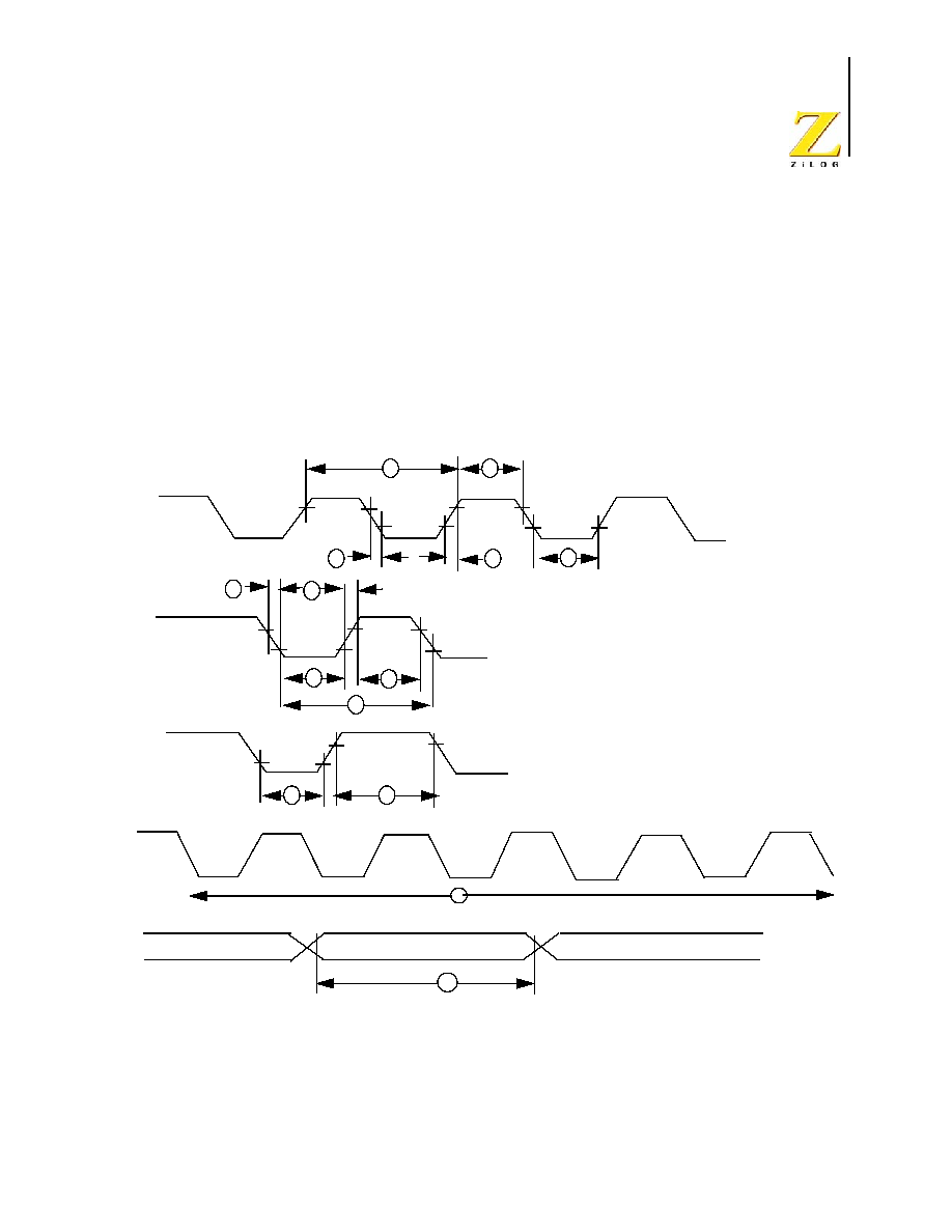
PS015601-1003
Z87C33
CMOS Z8" MCU Consumer Controller Processor
56
AC Electrical Characteristics
The timing characteristics with respect to external input/output sources are pro-
vided in the following pages.
Additional Timing
Figure 16 illustrates the timing characteristics with respect to system clock func-
tions. See Tables 39 and 40 for descriptions of the numbered timing parameters in
the figure.
Figure 16.Additional Timing
The values presented in Table 39 are within a standard temperature range of 0∫C
to 70∫C.
Clock
4
5
3
1
3
9
8
6
2
7
2
7
T
N
IRQ
N
Clock
Setup
11
12

PS015601-1003
Z87C33
CMOS Z8" MCU Consumer Controller Processor
57
Table 39. Additional Timing at Standard Temperature
No Sym
Parameter
V
CC
1
T
A
= 0∫C to
+70∫C
Units
Notes D1,D0
4 MHz
Min
Max
1
T
P
C
Input Clock Period
3.0V
250
DC
ns
2,3,4
5.5V
250
DC
ns
2,3,4
2
T
R
C,
T
F
C
Clock Input Rise & Fall
Times
3.0V
25
ns
2,3
5.5V
25
ns
2,3
3
T
W
C
Input Clock Width
3.0V
125
ns
2,3,4
5.5V
125
ns
2,3,4
4
T
W
T
IN
L
Timer Input Low Width 3.0V
100
ns
2,3
5.5V
70
ns
2,3
5
T
W
T
IN
H Timer Input High Width 3.0V
3T
P
C
2,3
5.5V
3T
P
C
2,3
6
T
P
T
IN
Timer Input Period
3.0V
4T
P
C
2,3
5.5V
4T
P
C
2,3
7
T
R
T
IN
,
T
F
T
IN
Timer Input Rise & Fall
Timer
3.0V
100
ns
2,3
5.5V
100
ns
2,3
8A T
W
IL
Interrupt Request Low
Time
3.0V
100
ns
2,3,5
5.5V
70
ns
2,3,5
8B T
W
IL
Interrupt Request Low
Time
3.0V
3T
P
C
2,3,6
5.5V
3T
P
C
2,3,6
Notes:
1. The VCC voltage specification of 3.0V guarantees 3.3V ±0.3V, and the VCC voltage
specification of 5.5V guarantees 5.0V ±0.5V.
2. Timing reference uses 0.7 VCC for a logic 1 and 0.2 VCC for a logic 0.
3. SMR: D1 = 0.
4. The maximum frequency for the external crystal clock is 4 MHz when using LOW-EMI OSCIL-
LATOR mode.
5. The interrupt request via Port 3 (P31≠P33).
6. The interrupt request via Port 3 (P30).
7. SMR: D5 = 1, and the POR Stop-Mode Delay is on.
8. For RC and LC oscillators, and for an oscillator driven by a clock driver.
9. The D1,D0 column applies to the Watch-Dog Timer Mode Register tap selection.
10. 12 µs is the typical delay time; only applies when SMR Register bit D5 is cleared to 0

PS015601-1003
Z87C33
CMOS Z8" MCU Consumer Controller Processor
58
The values presented in Table 40 are within the extended temperature range of ≠
40∫C to 105∫C.
9
T
W
IH
Interrupt Request Input
High Time
3.0V
3T
P
C
2,3,5
5.5V
3T
P
C
2,3,5
10
T
WSM
Stop-Mode Recovery
Width Spec
3.0V
12
ns
7
5.5V
12
ns
7
11
T
OST
Oscillator Startup Time 3.0V
5T
P
C
7,8
5.5V
5T
P
C
7,8
12
T
WDT
Watch-Dog Timer
Delay Timer before
time-out
3.0V
7
ms
9
0,0
5.5V
3.5
ms
9
0,0
3.0V
14
ms
9
0,1
5.5V
7
ms
9
0,1
3.0V
28
ms
9
1,0
5.5V
14
ms
9
1,0
3.0V
112
ms
9
1,1
5.5V
56
ms
9
1,1
13
T
POR
Power-On Reset Delay 3.0V
3
26
ms
5.5V
1.5
13
ms
Table 39. Additional Timing at Standard Temperature (Continued)
No Sym
Parameter
V
CC
1
T
A
= 0∫C to
+70∫C
Units
Notes D1,D0
4 MHz
Min
Max
Notes:
1. The VCC voltage specification of 3.0V guarantees 3.3V ±0.3V, and the VCC voltage
specification of 5.5V guarantees 5.0V ±0.5V.
2. Timing reference uses 0.7 VCC for a logic 1 and 0.2 VCC for a logic 0.
3. SMR: D1 = 0.
4. The maximum frequency for the external crystal clock is 4 MHz when using LOW-EMI OSCIL-
LATOR mode.
5. The interrupt request via Port 3 (P31≠P33).
6. The interrupt request via Port 3 (P30).
7. SMR: D5 = 1, and the POR Stop-Mode Delay is on.
8. For RC and LC oscillators, and for an oscillator driven by a clock driver.
9. The D1,D0 column applies to the Watch-Dog Timer Mode Register tap selection.
10. 12 µs is the typical delay time; only applies when SMR Register bit D5 is cleared to 0

PS015601-1003
Z87C33
CMOS Z8" MCU Consumer Controller Processor
59
Table 40. Additional Timing at Extended Temperature
No Sym
Parameter
V
CC
1
T
A
= ≠40∫C to
+105∫C
Units
Notes D1,D0
4 MHz
Min
Max
1
T
P
C
Input Clock Period
3.0V 250
DC
ns
2,3,4
5.5V 250
DC
ns
2,3,4
2
T
R
C,
T
F
C
Clock Input Rise & Fall
Times
3.0V
25
ns
2,3
5.5V
25
ns
2,3
3
T
W
C
Input Clock Width
3.0V 125
ns
2,3,4
5.5V 125
ns
2,3,4
4
T
W
T
IN
L
Timer Input Low Width 3.0V 100
ns
2,3
5.5V 70
ns
2,3
5
T
W
T
IN
H
Timer Input High Width 3.0V 3T
P
C
2,3
5.5V 3T
P
C
2,3
6
T
P
T
IN
Timer Input Period
3.0V 4T
P
C
2,3
5.5V 4T
P
C
2,3
7
T
R
T
IN
,
T
F
T
IN
Timer Input Rise & Fall
Timer
3.0V
100
ns
2,3
5.5V
100
ns
2,3
8A T
W
IL
Interrupt Request Low
Time
3.0V 100
ns
2,3,5
5.5V 70
ns
2,3,5
8B T
W
IL
Interrupt Request Low
Time
3.0V 3T
P
C
2,3,6
5.5V 3T
P
C
2,3,6
Notes:
1. The VCC voltage specification of 5.5V guarantees 5.0V ±0.5V.
2. The timing reference uses 0.7 VCC for a logic 1 and 0.2 VCC for a logic 0.
3. SMR: D1 = 0.
4. The maximum frequency for the external crystal clock is 4 MHz when using LOW-EMI OSCIL-
LATOR mode.
5. The interrupt request via Port 3 (P31≠P33).
6. The interrupt request via Port 3 (P30).
7. SMR: D5 = 1, and the POR Stop-Mode Delay is on.
8. For RC and LC oscillators, and for an oscillator driven by a clock driver.
9. The D1,D0 column applies to the Watch-Dog Timer Mode Register tap selection.
10. 12 µs is the typical delay time.

PS015601-1003
Z87C33
CMOS Z8" MCU Consumer Controller Processor
60
9
T
W
IH
Interrupt Request Input
High Time
3.0V 3T
P
C
2,3,5
5.5V 3T
P
C
2,3,5
10
T
WSM
Stop-Mode Recovery
Width Spec
3.0V 12
ns
7
5.5V 12
ns
7
11
T
OST
Oscillator Startup Time 3.0V
5T
P
C
7,8
5.5V
5T
P
C
7,8
12
T
WDT
Watch-Dog Timer
Delay Timer before
time-out
3.0V 7
ms
9
0,0
5.5V 3.5
ms
9
0,0
3.0V 14
ms
9
0,1
5.5V 7
ms
9
0,1
3.0V 28
ms
9
1,0
5.5V 14
ms
9
1,0
3.0V 112
ms
9
1,1
5.5V 56
ms
9
1,1
13
T
POR
Power-On Reset Delay 3.0V 2
32
ms
5.5V 1
16
ms
Table 40. Additional Timing at Extended Temperature (Continued)
No Sym
Parameter
V
CC
1
T
A
= ≠40∫C to
+105∫C
Units
Notes D1,D0
4 MHz
Min
Max
Notes:
1. The VCC voltage specification of 5.5V guarantees 5.0V ±0.5V.
2. The timing reference uses 0.7 VCC for a logic 1 and 0.2 VCC for a logic 0.
3. SMR: D1 = 0.
4. The maximum frequency for the external crystal clock is 4 MHz when using LOW-EMI OSCIL-
LATOR mode.
5. The interrupt request via Port 3 (P31≠P33).
6. The interrupt request via Port 3 (P30).
7. SMR: D5 = 1, and the POR Stop-Mode Delay is on.
8. For RC and LC oscillators, and for an oscillator driven by a clock driver.
9. The D1,D0 column applies to the Watch-Dog Timer Mode Register tap selection.
10. 12 µs is the typical delay time.
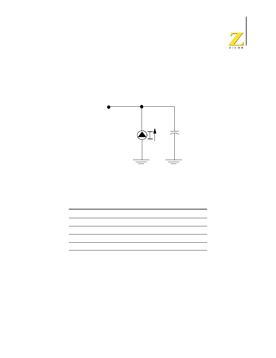
PS015601-1003
Z87C33
CMOS Z8" MCU Consumer Controller Processor
61
Standard Test Conditions
The characteristics listed in following pages apply for standard test conditions as
noted. All voltages are referenced to GND. Positive current flows into the refer-
enced pin (see Figure 17.)
Figure 17.Test Load Diagram
Capacitance
Packaging
Figure 18 illustrates the 28-pin DIP package.
Table 41. Capacitance*
Parameter
Min
Max
Input capacitance
0
12 pF
Output capacitance
0
12 pF
I/O capacitance
0
12 pF
Note: *TA = 25∫C, VCC = GND = 0V, f = 1.0 MHz, unmeasured pins to GND.
From Output
Under Test
150 pF
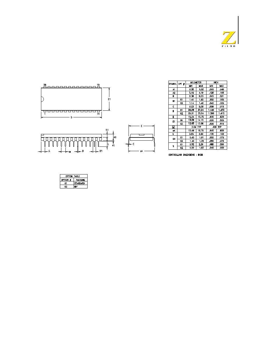
PS015601-1003
Z87C33
CMOS Z8" MCU Consumer Controller Processor
62
Figure 18.28-Pin DIP Package Diagram
Figure 19 illustrates the 28-pin SOIC package.

PS015601-1003
Z87C33
CMOS Z8" MCU Consumer Controller Processor
63
Figure 19.28-Pin SOIC Package Diagram
Ordering Information
Table 42. Ordering Information
Temperature
Speed (4MHz)
Pin Count
Package
Order Number*
Standard
4
28
DIP
Z87C3304PSC
Standard
4
28
SOIC
Z87C3304SSC
Extended
4
28
DIP
Z87C3304PEC
PS015601-1003
Z87C33
CMOS Z8" MCU Consumer Controller Processor
64
For fast results, contact your local ZiLOG sale office for assistance in ordering the
part(s) desired.
Part Number Description
ZiLOG part numbers consist of a number of components. For example, part num-
ber Z87C3304PEC is a 4-MHz 28-pin DIP that operates in the ≠40∫C to +105∫C
temperature range, with Plastic Standard Flow. The Z87C3304PEC part number
corresponds to the code segments indicated in the following table.
For fast results, contact your local ZiLOG sales office for assistance in ordering
the part required.
Precharacterization Product
The product represented by this document is newly introduced and ZiLOG has not
completed the full characterization of the product. The document states what
ZiLOG knows about this product at this time, but additional features or non-con-
formance with some aspects of the document may be found, either by ZiLOG or
its customers in the course of further application and characterization work. In
addition, ZiLOG cautions that delivery may be uncertain at times, due to start-up
yield issues.
Extended
4
28
SOIC
Z87C3304SEC
Note: *The Standard temperature range is 0∫C to 70∫C. For parts that operate in the Extended temperature range of
≠40∫C to 105∫C, substitute the letter E for the letter S. For example, the Order Number for a 28-pin DIP operating in
the Extended temperature range is Z87C3304PEC.
Z
ZiLOG Prefix
86
Z8 Product
C
ROM Product
33
Product Number
04
Speed (MHz)
P
Package
E
Temperature
C
Environmental Flow
Table 42. Ordering Information
Temperature
Speed (4MHz)
Pin Count
Package
Order Number*

PS015601-1003
Z87C33
CMOS Z8" MCU Consumer Controller Processor
65
ZiLOG, Inc.
532 Race Street
San Jose, CA 95126-3432
Telephone (408) 558-8500
FAX 408 558-8300
Internet:
www.ZiLOG.com
Document Information
Document Number Description
The Document Control Number that appears in the footer of each page of this
document contains unique identifying attributes, as indicated in the following
table:
Customer Feedback Form
Z87C33 Product Specification
If you experience any problems while operating this product, or if you note any
inaccuracies while reading this Product Specification, please copy and complete
this form, then mail or fax it to ZiLOG (see Return Information, below). We also
welcome your suggestions!
Customer Information
PS
Product Specification
00156 Unique Document Number
01
Revision Number
1003
Month and Year Published
Name
Country
Company
Phone
Address
Fax
City/State/Zip
E-Mail

PS015601-1003
Z87C33
CMOS Z8" MCU Consumer Controller Processor
66
Product Information
Return Information
ZiLOG
System Test/Customer Support
532 Race Street
San Jose, CA 95126-3432
Fax: (408) 558-8536
Email:
www.zilog.com
Problem Description or Suggestion
Provide a complete description of the problem or your suggestion. If you are
reporting a specific problem, include all steps leading up to the occurrence of the
problem. Attach additional pages as necessary.
_______________________________________________________________________________
_______________________________________________________________________________
_______________________________________________________________________________
_______________________________________________________________________________
_______________________________________________________________________________
_______________________________________________________________________________
Serial # or Board Fab #/Rev. #
Software Version
Document Number
Host Computer Description/Type