 | –≠–ª–µ–∫—Ç—Ä–æ–Ω–Ω—ã–π –∫–æ–º–ø–æ–Ω–µ–Ω—Ç: Z89139 | –°–∫–∞—á–∞—Ç—å:  PDF PDF  ZIP ZIP |

DS97TAD0201
P R E L I M I N A R Y
1
1
P
RELIMINARY
C
USTOMER
P
ROCUREMENT
S
PECIFICATION
Z89138/
1
Z89139 (ROMLESS)
V
OICE
P
ROCESSING
C
ONTROLLERS
FEATURES
s
Watch-Dog Timer and Power-On Reset
s
Improved Low-Power STOP Mode
s
On-Chip Oscillator that Accepts a Crystal or External
Clock Drive
s
Improved Global Power-Down Mode
s
Low-Power Consumption - 200 mW (typical)
s
Two Comparators
s
RAM and ROM Protect
s
On-Board Oscillator for 32.768 kHz Real-Time Clock
s
Clock Speeds of 20.48 or 29.49 MHz
s
16-Bit Digital Signal Processor (DSP)
s
6K Word DSP Program ROM
s
512 Words On-Chip DSP RAM
s
8-Bit A/D Converter with up to 16 kHz Sample Rate
s
10-Bit PWM D/A Converter
s
Six Vectored, Prioritized Z8 Interrupts
s
Three Vectored, Prioritized DSP Interrupts
s
Two DSP Timers to Support Different A/D and D/A
Sampling Rates
s
IBM
Æ
PC-Based Development Tools
s
Developer's Toolbox for T.A.M. Applications
IBM is a registered trademark of IBM Corporation.
GENERAL DESCRIPTION
The Z89138/Z89139 is a fully integrated, dual processor
controller designed for voice processing applications. The
I/O control processor is a Z8
Æ
MCU with 24 KB of program
memory, two 8-bit counter/timers, and up to 47 I/O pins.
The DSP is a 16-bit processor with a 24-bit ALU and accu-
mulator, 512x16 bits of RAM, single cycle instructions, and
6K words of program ROM. The chip also contains a half-
flash 8-bit A/D converter with up to a 16 kHz sample rate
and a 10-bit PWM D/A converter. The sampling rates for
the converters are programmable. The precision of the 8-
bit A/D can be extended by resampling the data at a lower
rate in software. The Z8 and DSP processors are coupled
by mailbox registers and an interrupt system. DSP or Z8
programs can be directed by events in each other's do-
main.
The Z89139 is the ROMless version of the Z89138. How-
ever, the on-chip DSP is not ROMless.
Notes:
All Signals with a preceding front slash, "/", are ac-
tive Low. For example, B//W (WORD is active Low); /B/W
(BYTE is active Low, only).
Device
ROM
(KB)
RAM*
(Bytes)
I/O
Lines
Voltage
Range
Z89138
24
256
47
4.5V to 5.5V
Z89139
256
47
4.5V to 5.5V
Note:
*General-Purpose

Z89138/Z89139
Voice Processing Controllers
Zilog
2
P R E L I M I N A R Y
DS97TAD0201
GENERAL DESCRIPTION
(Continued)
Power connections follow conventional descriptions be-
low:
Z8 Core Processor
The on-chip Z8 is Zilog's 8-bit microcontroller core with an
Expanded Register File to allow access to register-
mapped peripheral and I/O circuits. The Z8 offers a flexible
I/O scheme, an efficient register and address space struc-
ture and a number of ancillary features, which makes it
ideally suited for high-volume processing, peripheral con-
trollers, and consumer applications.
For applications demanding powerful I/O capabilities, the
Z89138 provides 47 pins dedicated to input and output.
These I/O lines are grouped into six ports. Each port is
configurable under software control to provide timing, sta-
tus signals and parallel I/O with or without handshake.
Four basic memory resources for the Z8 are available to
support a wide range of configurations: Program Memory,
Register File, Data Memory, and Expanded Register File.
The Z8 core processor is supported by an efficient register
file that allows any of 256 on-board data and control regis-
ters to be either the source and/or the destination of almost
any instruction. This unique architecture eliminates tradi-
tional microprocessor Accumulator bottlenecks and per-
mits rapid content switching.
The Register File is composed of 236 bytes of general-pur-
pose registers, four I/O port registers, and 15 control and
status registers. The Expanded Register File consists of
mailbox registers, WDT mode register, DSP Control regis-
ter, Stop-Mode Recovery register, Port Configuration reg-
ister, and the control and data registers for Port 4 and Port
5. Some of these registers are shared with the DSP.
To unburden the software from supporting real-time prob-
lems such as counting/timing and data communication, the
Z8 offers two on-chip counter/timers with a large number
of user-selectable modes.
Watch-Dog Timer and Stop-Mode Recovery features are
software driven by setting specific bits in control registers.
STOP and HALT instructions support reduced power op-
eration. The low-power Stop Mode allows parameter infor-
mation to be stored in the register file if power fails. An ex-
ternal capacitor or battery will retain device memory and
power the 32 kHz timer.
DSP Coprocessor
The DSP coprocessor is a second generation, 16-bit
two's- complement CMOS Digital Signal Processor (DSP).
Most instructions, including multiply and accumulate, are
accomplished in a single clock cycle. The processor con-
tains two on-chip data RAM blocks of 256 words, a 6K
word program ROM, 24-bit ALU, 16x16 multiplier, 24-bit
Accumulator, shifter, six-level stack, three vectored inter-
rupts and two inputs for conditional program jumps. Each
RAM block contains a set of four pointers which can be in-
cremented or decremented automatically to affect hard-
ware looping without software overhead. The data RAMs
can be simultaneously addressed and loaded to the multi-
plier for a true single-cycle scalar multiply.
Four external DSP registers are mapped into the expand-
ed register file of the Z8. Communication between the Z8
and the DSP occurs through those common registers that
form the mailbox registers.
The analog output is generated by a 10-bit resolution
Pulse Width Modulator (PWM). The PWM output is a digi-
tal signal with CMOS output levels. The output signal has
a resolution of 1 in 1024 with a sampling rate of 16 kHz
(XTAL = 20.48 MHz). The sampling rate can be changed
under software control and can be set at 10 and 16 kHz.
The dynamic range of the PWM is from 0 to 4V.
An 8-bit resolution half-flash A/D converter is provided.
The conversion is conducted with a sampling frequency of
16 kHz. (XTAL = 20.48 MHz) in order to provide oversam-
pling. The input signal is 4V peak to peak.
Two additional timers (Timer2 and Timer3) have been
added to support different sampling rates for the A/D and
D/A converters. These timers are free-running counters
that divide the crystal frequency to the appropriate sam-
pling of frequency. Two DSP I/O pins: DSP0, DSP1 are
provided for application.
Connection
Circuit
Device
Power
V
CC
V
DD
Ground
GND
V
SS
Z89138/Z89139
Zilog
Voice Processing Controllers
DS97TAD0201
P R E L I M I N A R Y
3
1
PIN DESCRIPTION
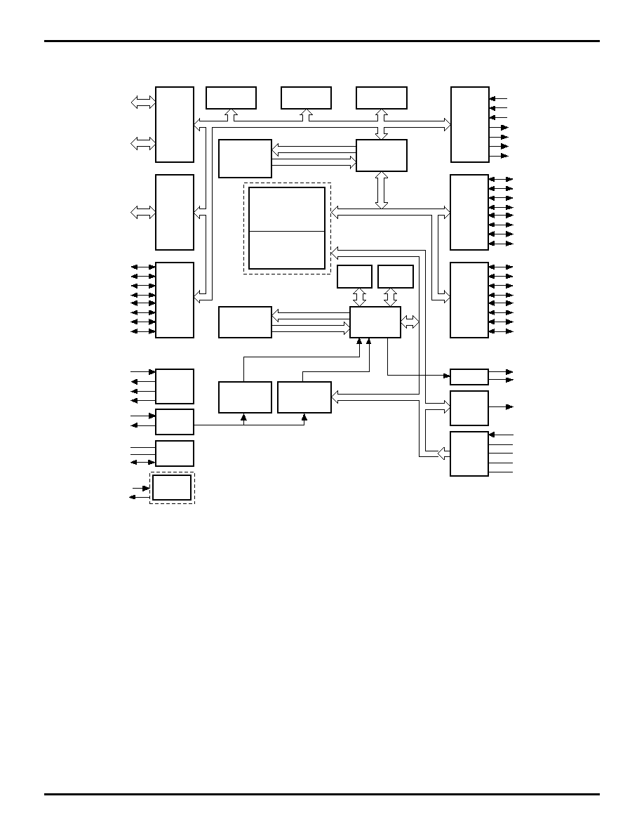
Figure 1. Z89138/139 Functional Block Diagram
Port 0
P00
P01
P02
P03
P04
P05
P06
P07
P10
P11
P12
P13
P14
P15
P16
P17
P20
P21
P22
P23
P24
P25
P26
P27
P31
P32
P33
P40
P41
P42
P43
P44
P45
P46
P47
P50
P51
P52
P53
P54
P55
P56
P57
RMLS
/AS
/DS
R/W
Timer 0
Capture Reg.
Port 3
Port 1
Port 4
Port 2
Port 5
Timer 1
Register File
256 x 8 Bit
24 Kbytes
Program
ROM
(Z89138)
Z8 Core
Register Bus
Internal Address Bus
Internal Data Bus
Expanded Register
File
(Z8)
Peripheral
Register
(DSP)
Expanded
Register Bus
Extended Bus of the DSP
6K Words
Program
ROM
DSP Core
Internal Address Bus
Internal Data Bus
DSP Port
PWM
(10-Bit)
ADC
(8-Bit)
Timer 2
Timer 3
Extended Bus of the DSP
Ext.
Memory
Control
OSC
Power
XTAL1
XTAL2
VDD
GND
/RESET
INT 1
INT 2
DSP0
DSP1
AN IN
AN VDD
AN GND
VREF+
VREF-
PWM
256 Word
RAM 0
256 Word
RAM 1
P34
P35
P36
P37
Input
Output
I/O
(Bit
Programmable)
I/O
(Bit
Programmable)
Address
or I/O
(Nibble
Programmable)
Address/Data
or I/O
(Byte
Programmable)
I/O
(Bit
Programmable)
mailbox
OSC1
OSC2
32 kHz
OSC
Z89138/Z89139
Voice Processing Controllers
Zilog
4
P R E L I M I N A R Y
DS97TAD0201
PIN DESCRIPTION
(Continued)
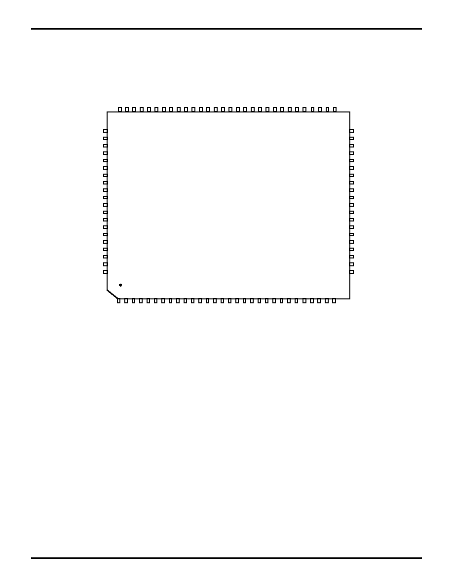
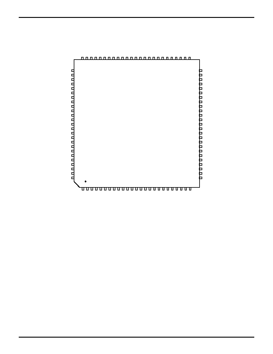
Figure 2. Z89138 100-Pin QFP Pin Configuration
50
45
40
35
31
81
85
90
95
100
P06
P05
P04
P03
P02
P01
P00
GND
P17
P16
P15
P14
P13
P12
P11
P10
GND
AGND
VREF-
ANIN
NC
NC
NC
VCC
P51
P50
P47
P46
P45
P44
P43
P42
P41
P40
P27
P26
P25
P24
P23
P22
VREF+
ANVDD
GND
PWM
RMLS
DSP1
DSP0
/AS
/DS
R//W
NC
P57
P56
P55
P54
VCC
XT
AL2
XT
AL1
P53
P52
P37
P36
P35
P34
P33
P32
P31
/RESET
P20
P21
P07
NC
NC
VCC
NC
NC
NC
NC
NC
NC
NC
NC
NC
NC
NC
NC
NC
NC
NC
NC
NC
NC
NC
NC
NC
OSC02
OSC01
GND
NC
NC
5
10
15
20
25
1
100-Pin QFP
30
75
70
65
60
55
80
51

Z89138/Z89139
Zilog
Voice Processing Controllers
DS97TAD0201
P R E L I M I N A R Y
5
1
Table 1. Z89138 100-Pin QFP Pin Identification
I/O Port
Symbol
Pin
Number
Direction
Function
GND
3, 53, 88, 97
Digital Ground
V
CC
16, 47, 77
Digital V
CC
= +5V
VREF+
1
Input/Output
Analog Voltage Ref+
ANV
DD
2
Analog V
DD
PWM
4
Output
PWM Output
RMLS
5
Input
Control Input
DSP1-0
6, 7
Output
DSP User Output 1, 0
/AS
8
Output
Address Strobe
/DS
9
Output
Data Strobe
R//W
10
Output
Read/Write
NC
11
No Connection
P57-P54
12-15
Input/Output
Port 5 Bit 7-4
XTAL2
17
Output
Crystal Output (20.48 or 29.49 MHz)
XTAL1
18
Input
Crystal Input (20.48 or 29.49 MHz)
P53-P52
19, 20
Input/Output
Port 5 Bit 3-2
P37-P34
21-24
Output
Port 3 Bit 7-4
P33-P31
25-27
Input
Port 3 Bit 3-1
/RESET
28
Input/Output
Reset
P20-P27
29-36
Input/Output
Port 2, Bit 0-7
P40-P47
37-44
Input/Output
Port 4, Bit 0-7
P50-P51
45, 46
Input/Output
Port 5, Bit 0-1
NC
48-52
No Connection
OSC1
54
Input
Crystal Input (32.768 kHz)
OSC2
55
Output
Crystal Output (32.768 kHz)
NC
56-76
No Connection
NC
78, 79
No Connection
P07-P00
80-87
Input/Output
Port 0, Bit 7-0
P17-P10
89-96
Input/Output
Port 1, Bit 7-0
ANGND
98
Analog GND
VREF-
99
Input
Analog Voltage Ref-
ANIN
100
Input
Analog Input
Z89138/Z89139
Voice Processing Controllers
Zilog
6
P R E L I M I N A R Y
DS97TAD0201
PIN DESCRIPTION
(Continued)
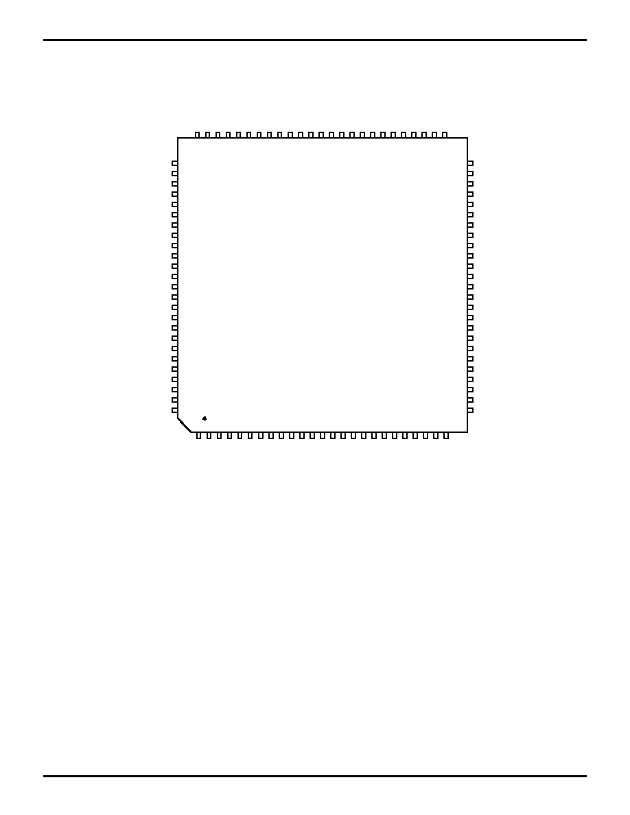
Figure 3. Z89138 100-Pin VQFP Pin Configuration
50
45
40
35
30
26
76
80
85
90
95
100
NC
NC
P07
P06
P05
P04
P03
P02
P01
P00
GND
P17
P16
P15
P14
P13
P12
P11
P10
GND
AGND
VREF-
ANIN
VREF+
ANVDD
NC
NC
NC
NC
NC
VCC
P51
P50
P47
P46
P45
P44
P43
P44
P45
P46
P47
P50
P51
VCC
NC
NC
NC
NC
NC
GND
PWM
RMLS
DSP1
DSP0
/AS
/DS
R//W
NC
P57
P56
P55
P54
VCC
XT
AL2
XT
AL1
P53
P52
P37
P36
P35
P34
P33
P32
P31
VCC
NC
NC
NC
NC
NC
NC
NC
NC
NC
NC
NC
NC
NC
NC
NC
NC
NC
NC
NC
NC
NC
OSC2
OSC1
GND
5
10
15
20
25
1
70
65
60
55
51
75
100-Pin VQFP

Z89138/Z89139
Zilog
Voice Processing Controllers
DS97TAD0201
P R E L I M I N A R Y
7
1
Table 2. Z89138 100-Pin VQFP Pin Identification
I/O Port
Symbol
Pin
Number
Direction
Symbol
GND
1, 51, 86, 95
Digital Ground
V
CC
14, 45, 75
Digital VCC = +5V
VREF+
99
Input/Output
Analog Voltage Ref+
ANV
DD
100
Analog VDD
PWM
2
Output
PWM Output
RMLS
3
Input
Control Input
DSP1-0
4, 5
Output
DSP User Output 1, 0
/AS
6
Output
Address Strobe
/DS
7
Output
Data Strobe
R//W
8
Output
Read/Write
NC
9
No Connection
P57-P54
10-13
Input/Output
Port 5 Bit 7-4
XTAL2
15
Output
Crystal Output (20.48 or
29.49 MHz)
XTAL1
16
Input
Crystal Input (20.48 or 29.49
MHz)
P53-P52
17, 18
Input/Output
Port 5 Bit 3-2
P37-P34
19-22
Output
Port 3 Bit 7-4
P33-P31
23-25
Input
Port 3 Bit 3-1
/RESET
26
Input/Output
Reset
P20-P27
27-34
Input/Output
Port 2, Bit 0-7
P40-P47
35-42
Input/Output
Port 4, Bit 0-7
P50-P51
43, 44
Input/Output
Port 5, Bit 0-1
NC
46-50
No Connection
OSC1
52
Input
Crystal Input (32.768 kHz)
OSC2
53
Output
Crystal Output (32.768 kHz)
NC
54-74
No Connection
NC
76, 77
No Connection
P07-P00
78-85
Input/Output
Port 0, Bit 7-0
P17-P10
87-94
Input/Output
Port 1, Bit 7-0
ANGND
96
Analog GND
VREF-
97
Input
Analog Voltage Ref-
ANIN
98
Input
Analog Input
Z89138/Z89139
Voice Processing Controllers
Zilog
8
P R E L I M I N A R Y
DS97TAD0201
PIN DESCRIPTION
(Continued)
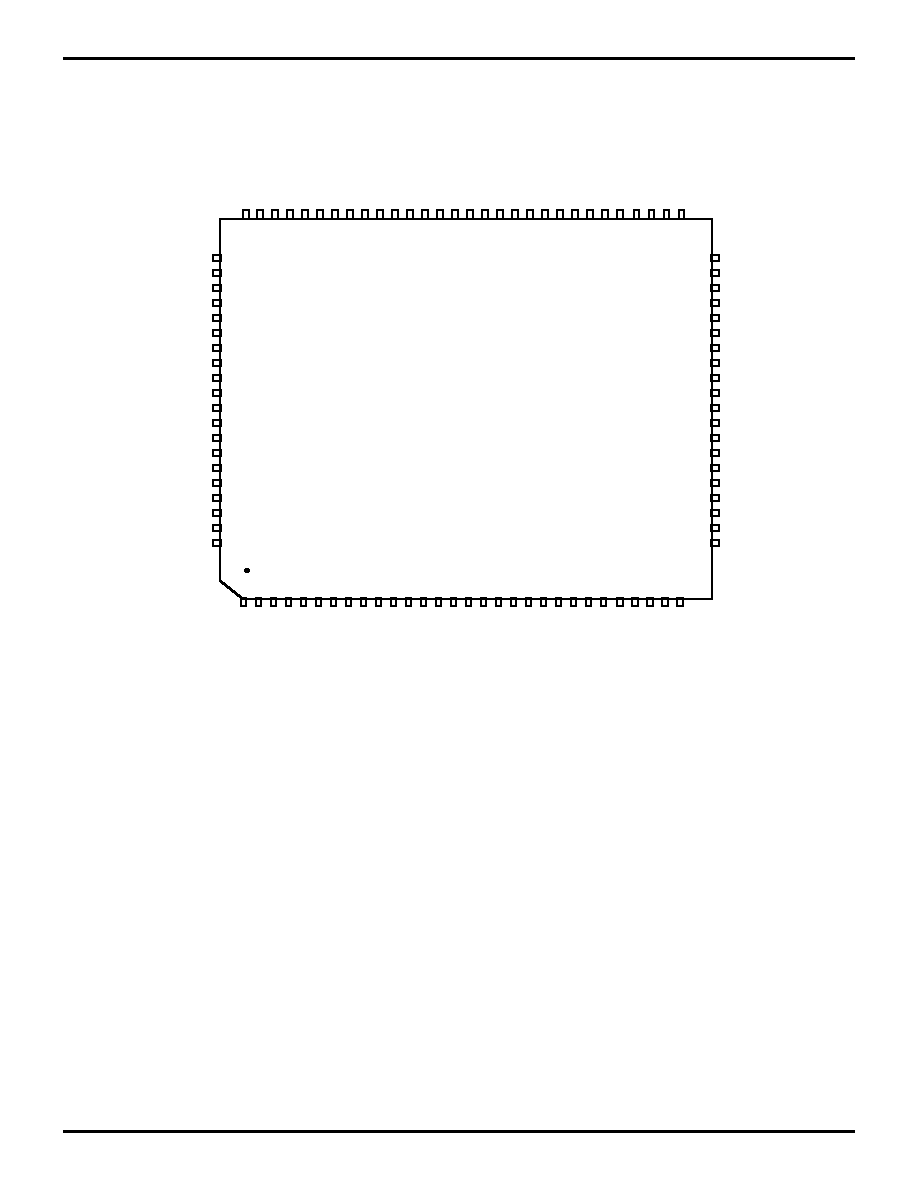
Figure 4. Z89139 100-Pin QFP Pin Configuration
50
45
40
35
31
81
85
90
95
100
P06
P05
P04
P03
P02
P01
P00
GND
P17
P16
P15
P14
P13
P12
P11
P10
GND
AGND
VREF-
ANIN
NC
NC
NC
VCC
P51
P50
P47
P46
P45
P44
P43
P42
P41
P40
P27
P26
P25
P24
P23
P22
VREF+
ANVDD
GND
PWM
VCC
DSP1
DSP0
/AS
/DS
R//W
NC
P57
P56
P55
P54
VCC
XT
AL2
XT
AL1
P53
P52
P37
P36
P35
P34
P33
P32
P31
/RESET
P20
P21
P07
NC
NC
VCC
NC
NC
NC
NC
NC
NC
NC
NC
NC
NC
NC
NC
NC
NC
NC
NC
NC
NC
NC
NC
NC
OSC02
OSC01
GND
NC
NC
5
10
15
20
25
1
100-Pin QFP
30
75
70
65
60
55
80
51

Z89138/Z89139
Zilog
Voice Processing Controllers
DS97TAD0201
P R E L I M I N A R Y
9
1
Table 3. Z89139 100-Pin QFP Pin Identification
I/O Port
Symbol
Pin Number
Direction
Function
GND
3, 53, 88, 97
Digital Ground
V
CC
5, 16, 47, 77
Digital V
CC
= +5V
VREF+
1
Input/Output
Analog Voltage Ref+
ANV
DD
2
Analog V
DD
PWM
4
Output
PWM Output
DSP1-0
6, 7
Output
DSP User Output 1, 0
/AS
8
Output
Address Strobe
/DS
9
Output
Data Strobe
R//W
10
Output
Read/Write
NC
11
No Connection
P57-P54
12-15
Input/Output
Port 5 Bit 7-4
XTAL2
17
Output
Crystal Output (20.48 or 29.49 MHz)
XTAL1
18
Input
Crystal Input (20.48 or 29.49 MHz)
P53-P52
19, 20
Input/Output
Port 5 Bit 3-2
P37-P34
21-24
Output
Port 3 Bit 7-4
P33-P31
25-27
Input
Port 3 Bit 3-1
/RESET
28
Input/Output
Reset
P20-P27
29-36
Input/Output
Port 2, Bit 0-7
P40-P47
37-44
Input/Output
Port 4, Bit 0-7
P50-P51
45, 46
Input/Output
Port 5, Bit 0-1
NC
48-52
No Connection
OSC1
54
Input
Crystal Input (32.768 kHz)
OSC2
55
Output
Crystal Output (32.768 kHz)
NC
56-76
No Connection
NC
78-79
No Connection
P07-P00
80-87
Input/Output
Port 0, Bit 7-0
P17-P10
89-96
Input/Output
Port 1, Bit 7-0
ANGND
98
Analog GND
VREF-
99
Input
Analog Voltage Ref-
ANIN
100
Input
Analog Input
Z89138/Z89139
Voice Processing Controllers
Zilog
10
P R E L I M I N A R Y
DS97TAD0201
PIN DESCRIPTION
(Continued)
Figure 5. Z89139 100-Pin VQFP Pin Configuration
50
45
40
35
30
26
76
80
85
90
95
100
NC
NC
P07
P06
P05
P04
P03
P02
P01
P00
GND
P17
P16
P15
P14
P13
P12
P11
P10
GND
AGND
VREF-
ANIN
VREF+
ANVDD
NC
NC
NC
NC
NC
VCC
P51
P50
P47
P46
P45
P44
P43
P42
P41
P40
P27
P26
P25
P24
P23
P22
P21
P20
/RESET
GND
PWM
VCC
DSP1
DSP0
/AS
/DS
R//W
NC
P57
P56
P55
P54
VCC
XT
AL2
XT
AL1
P53
P52
P37
P36
P35
P34
P33
P32
P31
VCC
NC
NC
NC
NC
NC
NC
NC
NC
NC
NC
NC
NC
NC
NC
NC
NC
NC
NC
NC
NC
NC
OSC2
OSC1
GND
5
10
15
20
25
1
70
65
60
55
51
75
100-Pin VQFP

Z89138/Z89139
Zilog
Voice Processing Controllers
DS97TAD0201
P R E L I M I N A R Y
11
1
Table 4. Z89139 100-Pin VQFP Pin Identification
I/O Port
Symbol
Pin Number
Direction
Function
GND
1, 51, 86, 95
Digital Ground
V
CC
3, 14, 45, 75
Digital V
CC
= +5V
VREF+
99
Input/Output
Analog Voltage Ref+
ANV
DD
100
Analog VDD
PWM
2
Output
PWM Output
DSP1-0
4, 5
Output
DSP User Output 1, 0
/AS
6
Output
Address Strobe
/DS
7
Output
Data Strobe
R//W
8
Output
Read/Write
NC
9
No Connection
P57-P54
10-13
Input/Output
Port 5 Bit 7-4
XTAL2
15
Output
Crystal Output (20.48 or 29.49 MHz)
XTAL1
16
Input
Crystal Input (20.48 or 29.49 MHz)
P53-P52
17, 18
Input/Output
Port 5 Bit 3-2
P37-P34
19-22
Output
Port 3 Bit 7-4
P33-P31
23-25
Input
Port 3 Bit 3-1
/RESET
26
Input/Output
Reset
P20-P27
27-34
Input/Output
Port 2, Bit 0-7
P40-P47
35-42
Input/Output
Port 4, Bit 0-7
P50-P51
43, 44
Input/Output
Port 5, Bit 0-1
NC
46-50
No Connection
OSC1
52
Input
Crystal Input (32.768 kHz)
OSC2
53
Output
Crystal Output (32.768 kHz)
NC
54-74
No Connection
NC
76, 77
No Connection
P07-P00
78-85
Input/Output
Port 0, Bit 7-0
P17-P10
87-94
Input/Output
Port 1, Bit 7-0
ANGND
96
Analog GND
VREF-
97
Input
Analog Voltage Ref-
ANIN
98
Input
Analog Input
Z89138/Z89139
Voice Processing Controllers
Zilog
12
P R E L I M I N A R Y
DS97TAD0201
ABSOLUTE MAXIMUM RATINGS
Stresses greater than those listed under Absolute Maxi-
mum Ratings can cause permanent damage to the device.
This is a stress rating only; operation of the device at any
condition above those indicated in the operational sections
of these specifications is not implied. Exposure to absolute
maximum rating conditions for an extended period can af-
fect device reliability.
STANDARD TEST CONDITIONS
The characteristics listed below apply for standard test
conditions as noted. All voltages are referenced to GND.
Positive current flows into the referenced pin (Figure 6).
CAPACITANCE
T
A
= 25
∞
C, V
CC
= GND = 0V, f = 1.0 MHz, unmeasured
pins returned to GND.
Sym
Description
Min
Max
Units
V
CC
Supply
Voltage (*)
≠0.3
+7.0
V
T
STG
Storage Temp
≠65
∞
+150
∞
C
T
A
Oper.
Ambient
Temp.
C
Notes:
*Voltage on all pins with respect to GND.
See Ordering Information.
Figure 6. Test Load Diagram
+5V
From Output
Under Test
150 pF
9.1 k
2.1 k
Parameter
Min
Max
Input capacitance
0
12 pF
Output capacitance
0
12 pF
I/O capacitance
0
12 pF

Z89138/Z89139
Zilog
Voice Processing Controllers
DS97TAD0201
P R E L I M I N A R Y
13
1
DC ELECTRICAL CHARACTERISTICS
V
CC
Note 1
T
A
= 0
∞
C to +55
∞
C
Typical
@ 25
∞
C
Sym
Parameter
Min
Max
Units
Conditions
I
CC
Supply Current
5.0V
65
40
mA
I
CC1
Halt Mode Current
5.0V
20
6
mA
I
CC2
Stop Mode Current
5.0V
20
6
µ
A
See Note 2
V
MAX
Max Input Voltage
5.0V
7
V
CH
Clock Input High
Voltage
5.0V
0.9 V
CC
V
CC
+0.3
2.5
V
Driven by External
Clock Generator
V
CL
Clock Input Low
Voltage
5.0V
GND ≠0.3
0.1 V
CC
1.5
V
Driven by External
Clock Generator
V
IH
Input High Voltage
5.0V
0.7 V
CC
V
CC
+0.3
2.5
V
V
IL
Input Low Voltage
5.0V
GND ≠0.3
0.2 V
CC
1.5
V
V
OH
Output High Voltage
5.0V
V
CC
≠0.4
4.8
V
I
OH
= ≠2.0 mA
V
OL1
Output Low Voltage
5.0V
0.4
0.1
V
I
OL
= +4.0 mA
V
OL2
Output Low Voltage
5.0V
1.2
0.3
V
I
OL
= +12 mA, 3 Pin
Max
V
RH
Reset Input High
Voltage
5.0V
.8 V
CC
V
CC
2.1
V
V
Rl
Reset Input Low
Voltage
5.0V
GND ≠0.3
0.2 V
CC
1.7
V
OFFSET
Comparator Input
Offset
5.0V
25
10
mV
Voltage
I
IL
Input Leakage
5.0V
≠10
10
10
µ
A
I
OL
Output Leakage
5.0V
≠10
10
10
µ
A
I
IR
Reset Input Current
5.0V
≠55
≠30
µ
A
Notes:
1. 5.0V
±
0.5V
2. When a 32 kHz crystal is used, additional value must be added to the STOP Mode current ICC2.
The sum will be 200
µ
A/max, 150
µ
A/typical.

Z89138/Z89139
Voice Processing Controllers
Zilog
14
P R E L I M I N A R Y
DS97TAD0201
DC ELECTRICAL CHARACTERISTICS
Z89138 A/D Converter
T
A
= 0
∞
C to +55
∞
C
Sym
Parameter
V
DD
Min
Max
Units
Conditions
I
IL
Input Leakage
Analog Input
5.5V
1.00
µ
A
ANV
DD
=
5.50
V
V
IN
=
0.00
V
V
REFH
=
5.50
V
V
REFL
= 0.00 V
I
IH
Input Leakage
Analog Input
5.5V
2.00
µ
A
ANV
DD
= 5.50 V
V
IN
=
5.50
V
V
REFH
=
5.50
V
V
REFL
=
0.00
V
I
VREFH
Input Current
5.5V
1.00
mA
V
IN
=
5.50
V
V
REFL
=
0.00
V
ANV
DD
=
5.50
V
I
VREFL
Input Current
5.5V
2
µ
A
V
IN
=
5.50
V
V
REFL
=
5.50
V
ANV
DD
=
5.50
V
I
VEFL
Input Current
5.5V
≠2.00
mA
V
IN
=
0.00
V
V
REFH
=
5.50
V
ANV
DD
=
0.00
V
I
VREFL
Input Current
5.5V
2
µ
A
V
IN
=
0.00
V
V
REFH
=
5.50
V
ANV
DD
=
5.50
V
Z89138/Z89139
Zilog
Voice Processing Controllers
DS97TAD0201
P R E L I M I N A R Y
15
1
DC ELECTRICAL CHARACTERISTICS
21 Other Non-Regular I/O
T
A
= 0
∞
C to +55
∞
C
Sym
Parameter
V
DD
Min
Max
Units
Conditions
I
IRH
Input Current ROMless Pin
5.5V
6.00
µ
A
V
IN
= 5.50 V
I
IR1
Input Current ROMless Pin
5.5V
6.00
µ
A
V
IN
= 0.00 V
I
IR
Input Current ROMless Pin
During Reset Active
5.5V
1.00
mA
V
IN
= 5.50 V
I
IHX2
Input Current
XTAL2 pin in STOP Mode
5.5V
1.00
µ
A
V
IN
= 0.00 V
I
ILX2
Input Current
XTAL2 Pin in STOP Mode
5.5V
1.00
µ
A
V
IN
= 5.50 V
I
IHX1
Input current
XTAL1 Pin
5.5V
30
µ
A
V
IN
= 0.00 V
I
ILX1
Input Current
XTAL1 Pin
5.5V
30
µ
A
V
IN
= 5.50 V
V
OLXR
Output Low
Voltage XTAL2 Reset Inactive
5.5V
1.20
V
I
OL
= 4.00 mA
V
OLX
Output Low
Voltage XTAL2 Reset Inactive
5.5V
0.60
V
I
OL
=1.00 mA
V
OHXR
Output High
Voltage XTAL2 Reset Inactive
5.5V
4.00
V
I
OH
= 4.00 mA
I
VOHX
Output High
Voltage XTAL2 Reset Inactive
5.5V
4.00
V
I
OH
=1.00 mA
I
IH
Input Current
P31, P32, P33
5.5V
1.00
µ
A
V
IN
= 5.50 V
I
IL
Input Current
P31, P32, P33
5.5V
1.00
µ
A
V
IN
= 0.00 V

Z89138/Z89139
Voice Processing Controllers
Zilog
16
P R E L I M I N A R Y
DS97TAD0201
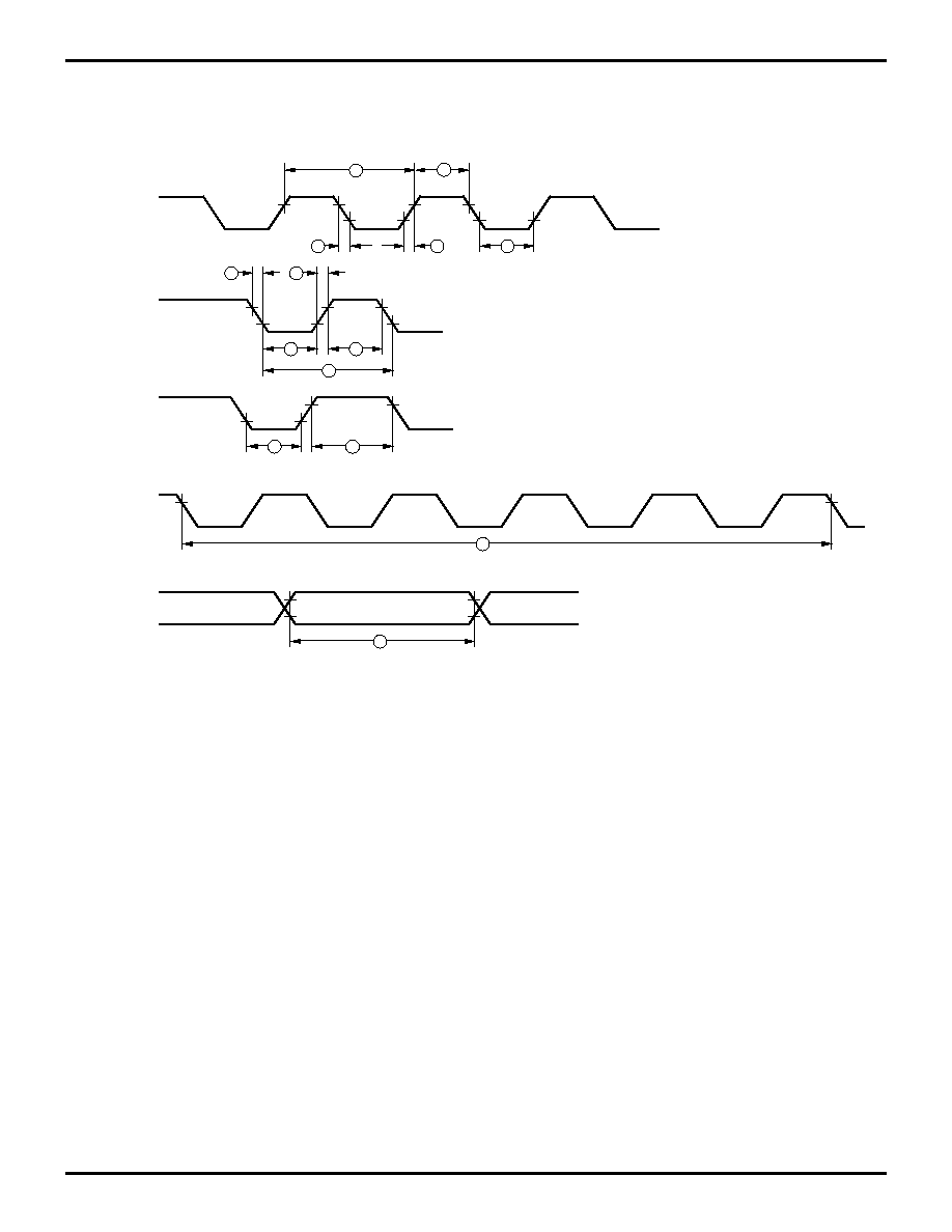
AC CHARACTERISTICS
External I/O or Memory Read and Write Timing Diagram
Figure 7. External I/O or Memory Read/Write Timing
R//W
9
12
19
3
16
13
4
5
8
18
11
6
17
10
15
7
14
1
Port 0, /DM
Port 1
/AS
/DS
(Read)
Port1
/DS
(Write)
A7 - A0
D7 - D0 IN
D7 - D0 OUT
A7 - A0
2

Z89138/Z89139
Zilog
Voice Processing Controllers
DS97TAD0201
P R E L I M I N A R Y
17
1
AC CHARACTERISTICS
External I/O or Memory Read and Write Timing Table
V
CC
T
A
= 0
∞
C to +55
∞
C
No
Symbol
Parameter
Note [4]
Min
Max
Units
Notes
1
TdA(AS)
Address Valid to /AS Rise Delay
5.0V
25
ns
2,3
2
TdAS(A)
/AS Rise to Address Float Delay
5.0V
35
ns
2,3
3
TdAS(DR)
/AS Rise to Read Data Req'd Valid
5.0V
150
ns
1,2,3
4
TwAS
/AS Low Width
5.0V
35
ns
2,3
5
TdAZ(DS)
Address Float to /DS Fall
5.0V
0
ns
6
TwDSR
/DS (Read) Low Width
5.0V
125
ns
1,2,3
7
TwDSW
/DS (Write) Low Width
5.0V
75
ns
1,2,3
8
TdDSR(DR)
/DS Fall to Read Data Req'd Valid
5.0V
90
ns
1,2,3
9
ThDR(DS)
Read Data to /DS Rise Hold Time
5.0V
0
ns
2,3
10
TdDS(A)
/DS Rise to Address Active Delay
5.0V
40
ns
2,3
11
TdDS(AS)
/DS Rise to /AS Fall Delay
5.0V
35
ns
2,3
12
TdR/W(AS)
R//W Valid to /AS Rise Delay
5.0V
25
ns
2,3
13
TdDS(R/W)
/DS Rise to R//W Not Valid
5.0V
35
ns
2,3
14
TdDW(DSW)
Write Data Valid to /DS Fall (Write) Delay
5.0V
40
ns
2,3
15
TdDS(DW)
/DS Rise to Write Data Not Valid Delay
5.0V
25
ns
2,3
16
TdA(DR)
Address Valid to Read Data Req'd Valid
5.0V
180
ns
1,2,3
17
TdAS(DS)
/AS Rise to /DS Fall Delay
5.0V
48
ns
2,3
18
TdDI(DS)
Data Input Setup to /DS Rise
5.0V
50
ns
1,2,3
19
TdDM(AS)
/DM Valid to /AS Fall Delay
5.0V
20
ns
2,3
Notes:
1. When using extended memory timing add 2 TpC.
2. Timing numbers given are for minimum TpC.
3. See clock cycle dependent characteristics table.
4. 5.0V
±
0.5 V.
Standard Test Load
All timing references use 0.9 V
CC
for a logic 1 and 0.1 V
CC
for a logic 0.
Z89138/Z89139
Voice Processing Controllers
Zilog
18
P R E L I M I N A R Y
DS97TAD0201
AC ELECTRICAL CHARACTERISTICS
Additional Timing Diagram
Figure 8. Additional Timing
Clock
1
3
4
8
2
2
3
TIN
IRQN
6
5
7
7
11
Clock
Setup
10
9
Stop
Mode
Recovery
Source
Z89138/Z89139
Zilog
Voice Processing Controllers
DS97TAD0201
P R E L I M I N A R Y
19
1
AC ELECTRICAL CHARACTERISTICS
Additional Timing Table
V
CC
T
A
= 0
∞
C to +55
∞
C
No
Sym
Parameter
Note 5
Min
Max
Units
Notes
1
TpC
Input Clock Period
5.0V
48.83
ns
1, 6
2
TrC,TfC
Clock Input Rise & Fall Times
5.0V
6
ns
1
3
TwC
Input Clock Width
5.0V
17
ns
1,7
4
TwTinL
Timer Input Low Width
5.0V
70
ns
5
TwTinH
Timer Input High Width
5.0V
3TpC
1
6
TpTin
Timer Input Period
5.0V
8TpC
1
7
TrTin, TfTin Timer Input Rise & Fall Timer
5.0V
100
ns
1
8a
TwIL
Int. Request Low Time
5.0V
70
ns
1,2
8b
TwIL
Int. Request Low Time
5.0V
3TpC
1
9
TwIH
Int. Request Input High Time
5.0V
3TpC
1
10
Twsm
Stop-Mode Recovery Width Spec
5.0V
12
ns
1
11
Tost
Oscillator Start-up Time
5.0V
5TpC
3
12
Twdt
Watch-Dog Timer
5.0V
5
ms
D1 = 0, D0 = 0 [4]
5.0V
15
ms
D1 = 0, D0 = 1 [4]
5.0V
25
ms
D1 = 1, D0 = 0 [4]
5.0V
100
ms
D1 = 1, D0 = 1 [4]
Notes:
1. Timing Reference uses 0.9 V
CC
for a logic 1 and 0.1 V
CC
for a logic 0.
2. Interrupt request via Port 3 (P31-P33).
3. SMR-D5 = 0
4. Reg. WDT
5. 5.0V
±
0.5 V
6. For 29.49 MHz, it will be 30.53 ns.
7. For 29.49 MHz, it will be 9 ns.

Z89138/Z89139
Voice Processing Controllers
Zilog
20
P R E L I M I N A R Y
DS97TAD0201
AC ELECTRICAL CHARACTERISTICS
Handshake Timing Diagrams
Figure 9. Input Handshake Timing
Data In
1
3
4
/DAV
(Input)
RDY
(Output)
Next Data In Valid
Delayed RDY
Delayed DAV
Data In Valid
5
6
2
Figure 10. Output Handshake Timing
Data Out
/DAV
(Output)
RDY
(Input)
Next Data Out Valid
Delayed RDY
Delayed DAV
Data Out Valid
7
8
9
10
11
Z89138/Z89139
Zilog
Voice Processing Controllers
DS97TAD0201
P R E L I M I N A R Y
21
1
AC ELECTRICAL CHARACTERISTICS
Handshake Timing Table
V
CC
T
A
= 0
∞
C to +55
∞
C
Data
No
Symbol
Parameter
Note
Min
Max
Units
Direction
1
TsDI(DAV)
Data In Setup Time
5.0V
0
ns
IN
2
ThDI(RDY)
RDY to Data Hold Time
5.0V
0
ns
IN
3
TwDAV
Data Available Width
5.0V
40
ns
IN
4
TdDAVI(RDY)
DAV Fall to RDY Fall Delay
5.0V
70
ns
IN
5
TdDAVId(RDY)
DAV Rise to RDY Rise Delay
5.0V
40
ns
IN
6
TdDO(DAV)
RDY Rise to DAV Fall Delay
5.0V
0
ns
IN
7
TcLDAV0(RDY)
Data Out to DAV Fall Delay
5.0V
TpC
ns
OUT
8
TcLDAV0(RDY)
DAV Fall to RDY Fall Delay
5.0V
0
ns
OUT
9
TdRDY0(DAV)
RDY Fall to DAV Rise Delay
5.0V
70
ns
OUT
10
TwRDY
RDY Width
5.0V
40
ns
OUT
11
TdRDY0d(DAV)
RDY Rise to DAV Fall Delay
5.0V
40
ns
OUT
Note: 5.0V
±
0.5V

Z89138/Z89139
Voice Processing Controllers
Zilog
22
P R E L I M I N A R Y
DS97TAD0201
PIN FUNCTIONS
/RESET (input, active Low). This pin initializes the MCU.
Reset is accomplished either through Power-On Reset
(POR), Watch-Dog Timer (WDT) reset, Stop-Mode Recov-
ery, or external reset. During POR and WDT Reset, the in-
ternally generated reset signal is driving the reset pin Low
for the POR time. Any devices driving the reset line must
be open-drain to avoid damage from a possible conflict
during reset conditions. A /RESET will reset both the Z8
and the DSP.
For the Z8: After the POR time, /RESET is a Schmitt-trig-
gered input. To avoid asynchronous and noisy reset prob-
lems, the Z8 is equipped with a reset filter of four external
clocks (4TpC). If the external reset signal is less than 4TpC
in duration, no reset occurs. On the fifth clock after the
/RESET is detected, an internal RST signal is latched and
held for an internal register count of 18 external clocks, or
for the duration of the external reset, whichever is longer.
Program execution begins at location 000CH (hexadeci-
mal), 5-10 TpC cycles after /RESET is released. The Z8
does not reset WDT, SMR, P2M, and P3M registers on a
Stop-Mode Recovery operation.
For the DSP: After POR, the DSP is in RUN mode. The Z8
controls the DSP commands to HALT, RUN or RESET.
When the DSP is in HALT mode, it cannot be woke up with
WDT or SMR.
RMLS ROMless (input, active High). This pin, when con-
nected to VDD, disables the internal Z8 ROM. (Note that,
when pulled Low to GND, the device functions normally as
the ROM version.) The DSP cannot be configured as
ROMless. This pin is only available on the Z89138.
R//W Read/Write (output, write Low). The R//W signal de-
fines the signal flow when the Z8 is reading or writing to an
external program or data memory. The Z8 is reading when
this pin is High and writing when this pin is Low.
/AS Address Strobe (output, active Low). Address Strobe
is pulsed once at the beginning of each machine cycle. Ad-
dress output is through Port 0/Port 1 for all external pro-
grams. Memory address transfers are valid at the trailing
edge of /AS. Under program control, /AS is placed in the
high-impedance state along with Ports 0 and 1, Data
Strobe, and Read/Write.
/DS Data Strobe (output, active Low). Data Strobe is acti-
vated once for each external memory transfer. For read
operations, data must be available prior to the trailing edge
of /DS. For write operations, the falling edge of /DS indi-
cates that output data is valid.
XTAL1 Crystal 1 (time-based input). This pin connects a
parallel-resonant crystal, ceramic resonator, LC, RC net-
work, or an external single-phase clock to the on-chip os-
cillator input.
XTAL2 Crystal 2 (time-based output). This pin connects a
parallel-resonant, crystal, ceramic resonant, or LC network
to the on-chip oscillator output.
DSP0 (output). DSP0 is a general-purpose output pin con-
nected to bit 6 of the Analog Control Register (DSP EXT4).
This bit has no special significance and can be used to out-
put data by writing to bit 6 of the ACR.
DSP1 (output). DSP1 is a general-purpose output pin con-
nected to bit 7 of the Analog Control Register (DSP EXT4).
This bit has no special significance and can be used to out-
put data by writing to bit 7 of the ACR.
PWM Pulse Width Modulator (Output). The PWM is a 10-
bit resolution D/A converter. This output is a digital signal
with CMOS output levels.
AN
IN
(input). Analog input for the A/D converter.
ANV
DD
. Analog power supply for the A/D converter.
VREF+ (input). Reference voltage (High) for the A/D con-
verter.
V
DD
. Digital power supply for the Z89138.
GND. Digital ground for the Z89138.
OSC1 Oscillator 1 (time-based input). This pin connects a
parallel-resonant crystal, ceramic resonator, LC, RC net-
work to the on-chip oscillator input.
OSC2 Oscillator 2 (time-based output). This pin connects
a parallel-resonant crystal, ceramic resonator, LC, RC net-
work to the on-chip oscillator output.
NC No Connect. For the 100-pin QFP package, pins 63
through 76, and pins 78 and 79 should be tied to Ground.
Other NC pins must float.

Z89138/Z89139
Zilog
Voice Processing Controllers
DS97TAD0201
P R E L I M I N A R Y
23
1
Port 0 (P07-P00). Port 0 is an 8-bit, bidirectional, CMOS
compatible port. These eight I/O lines are configured un-
der software control as a nibble I/O port, or as an address
port for interfacing external memory. The input buffers are
Schmitt-triggered and the output drivers are push-pull.
Port 0 is placed under handshake control. In this configu-
ration, Port 3, lines P32 and P35 are used as the hand-
shake control /DAV0 and RDY0. Handshake signal direc-
tion is dictated by the I/O direction to Port 0 of the upper
nibble P07-P04. The lower nibble must have the same di-
rection as the upper nibble.
The Auto Latch on Port 0 puts valid CMOS levels on all
CMOS inputs which are not externally driven. Whether this
level is 0 or 1 cannot be determined. A valid CMOS level,
rather than a floating node, reduces excessive supply cur-
rent flow in the input buffer.
For external memory references, Port 0 provides address
bits A11-A8 (lower nibble) or A15-A8 (lower and upper nib-
ble) depending on the required address space. If the ad-
dress range requires 12 bits or less, the upper nibble of
Port 0 can be programmed independently as I/O while the
lower nibble is used for addressing. If one or both nibbles
are needed for I/O operation, they are configured by writ-
ing to the Port 0 mode register.
In ROMless mode, after a hardware reset, Port 0 is config-
ured as address lines A15-A8, and extended timing is set
to accommodate slow memory access. The initialization
routine can include reconfiguration to eliminate this ex-
tended timing mode. (In ROM mode, Port 0 is defined as
input after reset.)
Port 0 is set in the high-impedance mode if selected as an
address output state along with Port 1 and the control sig-
nals /AS, /DS, and R//W (Figure 11).
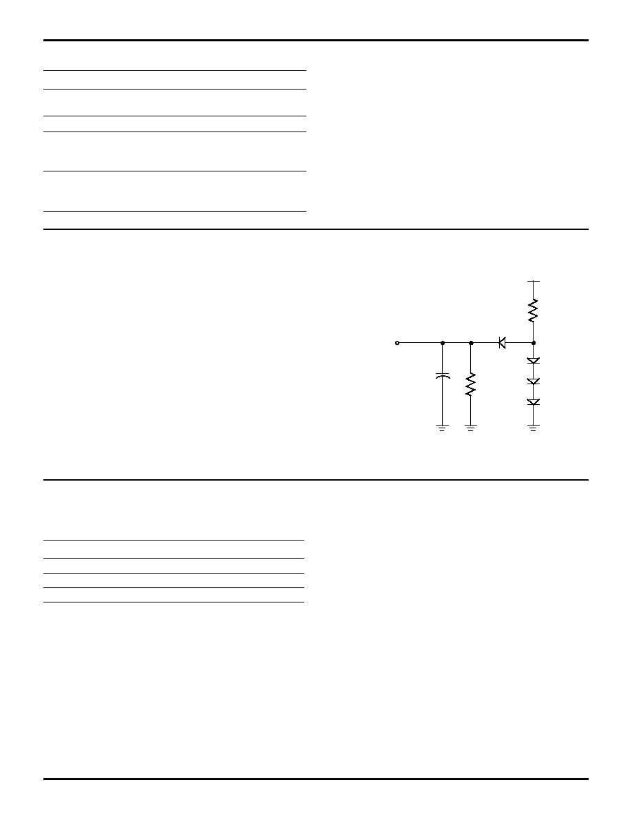
Figure 11. Port 0 Configuration
OEN
Out
In
Pad
Auto Latch
Port 0
(I/O or A15 - A8)
Handshake Controls
/DAV0 and RDY0
(P32 and P35)
Z89138/139
MCU
4
4
R = 500 K
1.5 2.3V Hysteresis

Z89138/Z89139
Voice Processing Controllers
Zilog
24
P R E L I M I N A R Y
DS97TAD0201
PIN FUNCTIONS (Continued)
Port 1 (P17-P10). Port 1 is an 8-bit, bidirectional, CMOS
compatible port (Figure 12). It has multiplexed Address
(A7-A0) and Data (D7-D0) ports. These eight I/O lines are
programmed as inputs or outputs, or can be configured un-
der software control as an Address/Data port for interfac-
ing external memory. The input buffers are Schmitt-trig-
gered and the output drivers are push-pull.
Port 1 can be placed under handshake control. In this con-
figuration, Port 3, lines P33 and P34 are used as the hand-
shake controls RDY1 and /DAV1 (Ready and Data Avail-
able). Memory locations greater than 24575 (Z89138) (in
ROM mode) are referenced through Port 1. To interface
external memory, Port 1 must be programmed for the mul-
tiplexed Address/Data mode. If more than 256 external lo-
cations are required, Port 0 outputs the additional lines.
Port 1 can be placed in the high-impedance state along
with Port 0, /AS, /DS, and R//W, allowing the Z89138/139
to share common resources in multiprocessor and DMA
applications.
Figure 12. Port 1 Configuration
OEN
Out
In
Pad
Auto Latch
Handshake Controls
/DAV2 and RDY2
(P31 and P36)
Z89138/139
MCU
R = 500 k
1.5 2.3V Hysteresis
Port 1
(I/O or AD7 - AD0)
8

Z89138/Z89139
Zilog
Voice Processing Controllers
DS97TAD0201
P R E L I M I N A R Y
25
1
Port 2 (P27-P20). Port 2 is an 8-bit, bidirectional, CMOS
compatible I/O port. These eight I/O lines are configured
under software control independently as inputs or outputs.
Port 2 is always available for I/O operation. The input buff-
ers are Schmitt-triggered. Bits programmed as outputs can
be globally programmed as either push-pull or open-drain.
Port 2 can be placed under handshake control. In this con-
figuration, Port 3 lines P31 and P36 are used as the hand-
shake controls lines /DAV2 and RDY2. The handshake
signal assignment for Port 3 lines P31 and P36 is dictated
by the direction (input or output) assigned to bit 7, Port 2
(Figure 13).
The Auto Latch on Port 2 puts valid CMOS levels on all
CMOS inputs which are not externally driven. Whether this
level is 0 or 1, cannot be determined. A valid CMOS level,
rather than a floating node, reduces excessive supply cur-
rent flow in the input buffer.
Figure 13. Port 2 Configuration
OEN
Out
In
Pad
Auto Latch
Port 2
(I/O)
Handshake Controls
/DAV2 and RDY2
(P31 and P36)
Z89138/139
MCU
R = 500 K
1.5 2.3V Hysteresis
Open-Drain

Z89138/Z89139
Voice Processing Controllers
Zilog
26
P R E L I M I N A R Y
DS97TAD0201
PIN FUNCTIONS (Continued)
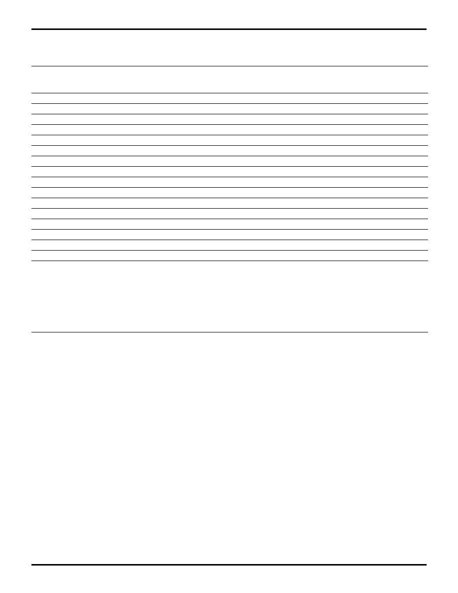
Port 3 (P37-P31). Port 3 is a 7-bit, CMOS compatible port
with three fixed inputs (P33-P31) and four fixed outputs
(P37-P34). It is configured under software control for in-
put/output, counter/timers, interrupt, and port handshakes.
Pins P31, P32, and P33 are standard CMOS inputs; out-
puts are push-pull.
Two on-board comparators can process analog signals on
P31 and P32 with reference to the voltage on P33. The an-
alog function is enabled by programming bit 1 of the Port 3
Mode Register. Port 3, pin 3 is a falling edge interrupt in-
put. P31 and P32 are programmable as rising, falling or
both edge-triggered interrupts (IRQ register bits 6 and 7).
P33 is the comparator reference voltage input. Access to
counter/timer1 is made through P31 (T
IN
) and P36 (T
OUT
).
Handshake lines for ports 0, 1, and 2 are available on P31
through P36.
Port 3 also provides the following control functions: hand-
shake for Ports 0, 1, and 2 (/DAV and RDY); three external
interrupt request signals (IRQ3-IRQ1); timer input and out-
put signals (T
IN
and T
OUT
) (Figure 14).
Comparator Inputs. Port 3, pins P31 and P32 all have a
comparator front end. The comparator reference voltage,
pin P33, is common to both comparators. In analog mode,
P31 and P32 are the positive inputs to the comparators
and P33 is the reference voltage supplied to both compar-
ators. In digital mode, pin P33 can be used as a P33 reg-
ister input or IRQ1 source.
Table 5. Port 3 Pin Assignments
Pin
I/O
CTC1
AN IN
Int.
P0 HS
P1 HS
P2 HS
EXT
P31
IN
T
IN
AN1
IRQ2
D/R
P32
IN
AN2
IRQ0
D/R
P33
IN
REF
IRQ1
D/R
P34
OUT
R/D
DM
P35
OUT
R/D
P36
OUT
T
OUT
R/D
P37
OUT
Notes:
HS = Handshake Signals
D = DAV
R = RDY
Z89138/Z89139
Zilog
Voice Processing Controllers
DS97TAD0201
P R E L I M I N A R Y
27
1
Figure 14. Port 3 Configuration
D1
R247 = P3M
P31 (AN1)
P32 (AN2)
P33 (REF)
From Stop Mode
Recovery Source
1 = Analog
0 = Digital
IRQ2, T
IN
, P31 Data
Latch
IRQ0, P32 Data Latch
IRQ1, P33 Data Latch
DIG.
AN.
Port 3
(I/O or Control)
Z89138/139
MCU
-
+
-
+
1
2
3
4
5
6
7
Z89138/Z89139
Voice Processing Controllers
Zilog
28
P R E L I M I N A R Y
DS97TAD0201
PIN FUNCTIONS (Continued)
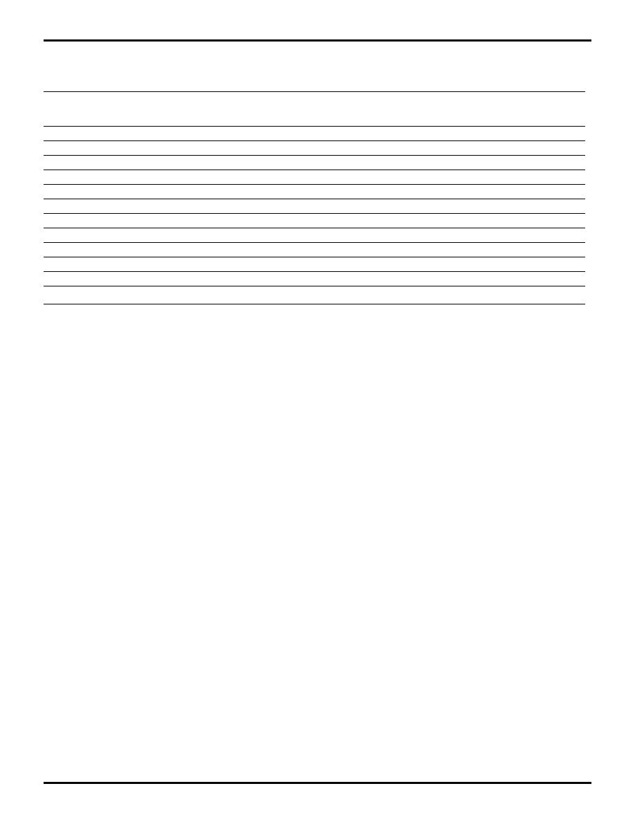
Port 4 (P47-P40). Port 4 is an 8-bit, bidirectional, CMOS
compatible I/O port (Figure 15). These eight I/O lines are
configured under software control independently as inputs
or outputs. Port 4 is always available for I/O operation. The
input buffers are Schmitt-triggered. Bits programmed as
outputs can be globally programmed as either push-pull or
open-drain.
Port 4 is a bit programmable general-purpose I/O port. The
control registers for Port 4 are mapped into the expanded
register file (Bank F) of the Z8.
Auto Latch. The Auto Latch on Port 4 puts valid CMOS
levels on all CMOS inputs which are not externally driven.
Whether this level is 0 or 1 cannot be determined. A valid
CMOS level, rather than a floating node, reduces exces-
sive supply current flow in the input buffer.
Figure 15. Port 4 Configuration
OEN
Out
In
Pad
Auto Latch
Port 4
(I/O)
Z89138/139
MCU
R = 500 K
1.5 2.3V Hysteresis
Open-Drain
Z89138/Z89139
Zilog
Voice Processing Controllers
DS97TAD0201
P R E L I M I N A R Y
29
1
Port 5 (P53-P50). Port 5 is a 4-bit, bidirectional, CMOS
compatible I/O port (Figure 16). These four I/O lines are
configured under software control independently as inputs
or outputs. Port 5 is always available for I/O operation. The
input buffers are Schmitt-triggered. Bits programmed as
outputs can be globally programmed as either push-pull or
open-drain.
Port 5 is a bit programmable general-purpose I/O port. The
control registers for Port 5 are mapped into the expanded
register file (Bank F) of the Z8.
Auto Latch. The Auto Latch on Port 5 puts valid CMOS
levels on all CMOS inputs which are not externally driven.
Whether this level is 0 or 1 cannot be determined. A valid
CMOS level, rather than a floating node, reduces exces-
sive supply current flow in the input buffer.
Figure 16. Port 5 Configuration
OEN
Out
In
Pad
Auto Latch
Port 5
(I/O)
Z89138/139
MCU
R = 500 K
1.5 2.3V Hysteresis
Open-Drain
Z89138/Z89139
Voice Processing Controllers
Zilog
30
P R E L I M I N A R Y
DS97TAD0201
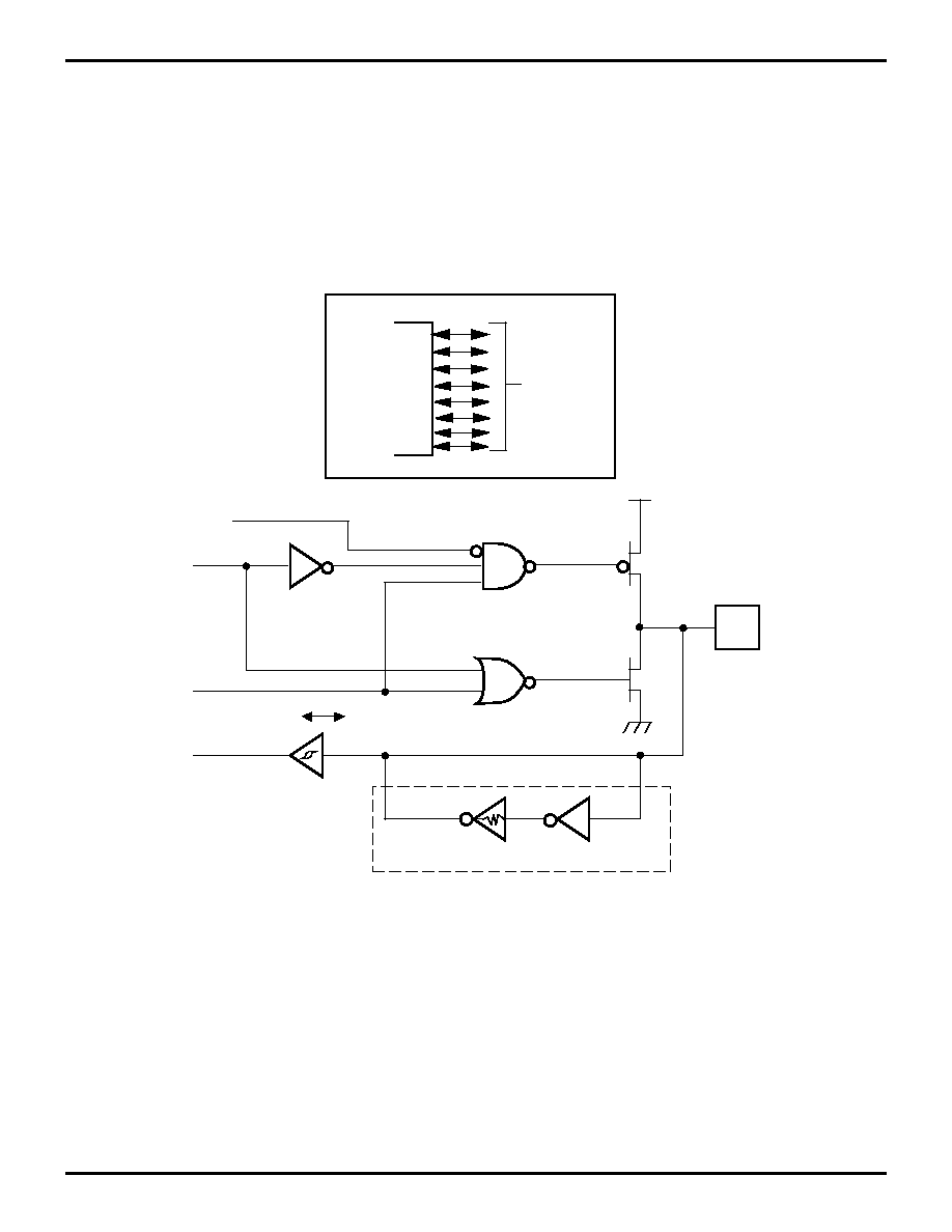
Z8 FUNCTIONAL DESCRIPTION
The Z8 core of the Z89138/139 incorporates special func-
tions to enhance the Z8's application in a variety of voice-
processing applications.
Reset. The device is reset in one of the following condi-
tions:
s
Power-On Reset
s
Watch-Dog Timer
s
Stop-Mode Recovery Source
s
External Reset
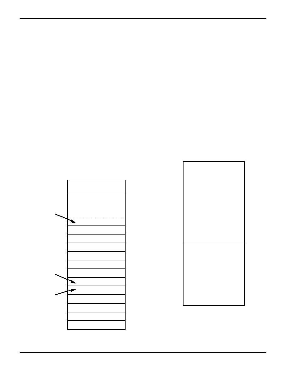
Program Memory. The Z8 addresses up to 24 KB of inter-
nal program memory and 40 KB external memory (Figure
17). The first 12 bytes of program memory are reserved for
the interrupt vectors. These locations contain six 16-bit
vectors which correspond to the five user interrupts and
one DSP interrupt. Byte 12 to byte 24575 consist of on-
chip mask-programmed ROM. At addresses 24576 and
greater the Z8 executes external program memory. In
ROMless mode, the Z8 will execute external program
memory beginning at byte 12 and continuing through byte
65535.
ROM Protect. The 24 KB of internal program memory for
the Z8 is mask programmable. A ROM protect feature pre-
vents "dumping" of the ROM contents of Program Memory
by inhibiting execution of LDC, LDCI, LDE, and LDEI in-
structions. The ROM Protect option is mask-programma-
ble, to be selected by the customer at the time the ROM
code is submitted.
Data Memory (/DM). In ROM Mode, the Z8 can address
up to 40 KB of external data memory beginning at location
24576 (Figure 18). In ROMless mode, the Z8 can address
the full 64 KB of external data memory beginning at loca-
tion 12. External data memory can be included with, or
separated from, the external program memory space.
/DM, an optional I/O function that can be programmed to
appear on Port 34, is used to distinguish between data and
program memory space. The state of the /DM signal is
controlled by the type of instruction being executed. An
LDC opcode references PROGRAM (/DM inactive) mem-
ory, and an LDE instruction references data (/DM active
Low) memory (Figure 18).
Figure 17. Program Memory
12
11
10
9
8
7
6
5
4
3
2
1
0
On-Chip
ROM
In ROM Mode
Location of
First Byte of
Instruction
Executed
After RESET
Interrupt
Vector
(Lower Byte)
Interrupt
Vector
(Upper Byte)
IRQ5
IRQ4
IRQ4
IRQ3
IRQ3
IRQ2
IRQ2
IRQ1
IRQ1
IRQ0
IRQ0
IRQ5
24575
External
ROM and RAM
65535
Figure 18. Data Memory Map
65535
24575
0
External
Data
Memory
Not Addressable
(In ROM Mode)
Z89138/Z89139
Zilog
Voice Processing Controllers
DS97TAD0201
P R E L I M I N A R Y
31
1
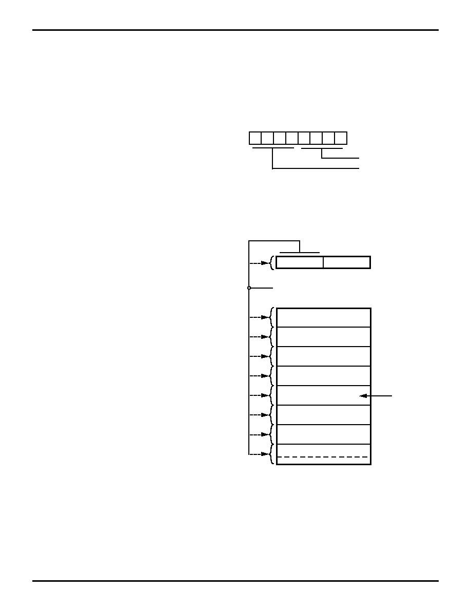
Register File. The standard Z8 register file consists of four
I/O port registers, 236 general-purpose registers, and 15
control and status registers (R0-R3, R4-R239, and R241-
R255, respectively). The instructions access registers di-
rectly or indirectly through an 8-bit address field. This al-
lows a short, 4-bit register address using the Register
Pointer (Figure 19). In the 4-bit mode, the register file is
divided into 16 working register groups, each occupying 16
continuous locations. The Register Pointer addresses the
starting location of the active working register group (Fig-
ure 20).
Note: Register Group E (Registers EF-E0) is only access-
ed through a working register and indirect addressing
modes.
RAM Protect. The upper portion of the Z8's RAM address
spaces 80H to EFH (excluding the control registers) is pro-
tected from reading and writing. The RAM Protect bit op-
tion is mask-programmable and is selected by the custom-
er when the ROM code is submitted. After the mask option
is selected, the user activates the RAM Protect from the in-
ternal ROM code by loading a bit D6 in the IMR register to
either a 0 (OFF) or a 1 (ON). A 1 in D6 indicates RAM Pro-
tect enabled.
Stack. The Z8's external data memory or the internal reg-
ister file is used for the stack. The 16-bit Stack Pointer
(R255-R254) is used for the external stack which can re-
side only from 24576 to 65535 in ROM mode or 0 to 65535
in ROMless mode. An 8-bit Stack Pointer (R255) is used
for the internal stack residing within the 236 general-pur-
pose registers (R239-R4). SPH can be used as a general-
purpose register when using internal stack only.
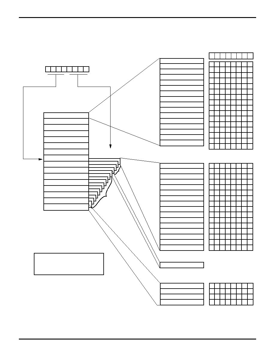
Expanded Register File. The register file on the Z8 has
been expanded to allow for additional system control reg-
isters and for mapping of additional peripheral devices
along with I/O ports into the register address area. The Z8
register address space has been implemented as 16
banks of 16 register groups per bank (Figure 20). These
register banks are known as the ERF (Expanded Register
File). Bits 7-4 of register RP (Register Pointer) select the
working register group. Bits 3-0 of register RP select the
Expanded Register bank (Figure 21).
The SMR register, WDT Register, control and data regis-
ters for Port 4 and Port 5, and the DSP control register are
located in Bank F of the Expanded Register File. Bank B
of the Expanded Register File consists of the Mailbox In-
terface through which the Z8 and the DSP communicate.
The rest of the Expanded Register is not physically imple-
mented and is open for future expansion.
Figure 19. Register Pointer Register
Figure 20. Register Pointer
D7 D6
D5
D4
D3
D2
D1
D0
R253 RP
Expanded Register File Bank
Working Register Group
The upper nibble of the register file address
provided by the register pointer specifies
the active working-register group
r7
r6
r5
r4
R253
R239
I/O Ports
Specified Working
Register Group
The upper nibble
of the register
file address
provided by the
instruction points
to the specified
working-register
group
R15
R3
R255
R240
r3
r2
r1
r0
Group 15 (F) Control Registers
Group 14 (E)
Group 13 (D)
Group 4 (4)
Group 3 (3)
Group 2 (2)
Group 1 (1)
Group 0 (0)
R223
R79
R63
R47
R31
R0
Z89138/Z89139
Voice Processing Controllers
Zilog
32
P R E L I M I N A R Y
DS97TAD0201
Z8 FUNCTIONAL DESCRIPTION (Continued)
Figure 21. Expanded Register File Architecture
7
6
5
4
3
2
1
0
Working Register
Group Pointer
Expanded Register
Bank Pointer
FFH
FOH
7FH
0FH
00H
Z8 Reg. File
REGISTER POINTER
FFH
FEH
FDH
FCH
FBH
FAH
F9H
F8H
F7H
F6H
F5H
% F4
F3H
F2H
F1H
F0H
SPL
SPH
RP
FLAGS
IMR
IRQ
IPR
P01M
P3M
P2M
PRE0
T0
PRE1
T1
TMR
(F) 0FH
(F) 0EH
(F) 0DH
(F) 0CH
(F) 0BH
(F) 0AH
(F) 09H
(F) 08H
(F) 07H
(F) 06H
(F) 05H
(F) 04H
(F) 03H
(F) 02H
(F) 01H
(F) 00H
WDTMR
SMR
U
U
U
0
1
1
0
1
0
0
1
0
0
0
0
0
REGISTER GROUP 0 (0)
Z8 EXPANDED REGISTER BANK (F)
RESET CONDITION
Z8 STANDARD REGISTER BANK (0)
REGISTER GROUP 15(F)
Z8 STANDARD CONTROL REGISTERS
Reserved
*
*
*
*
Reserved
HSEC
Reserved
DSP CON
Reserved
Reserved
Reserved
Reserved
P45CON
P5M
P5
P4M
P4
Reserved
PCON
REGISTER BANK (0)
U
U
U
1
U
U
U
U
U
U
U
0
U
U
U
0
1
1
1
1
1
1
1
1
U
U
U
U
U
U
U
U
1
1
1
1
1
1
1
1
U
U
U
U
U
U
U
U
1
1
1
1
1
1
1
0
0
1
2
3
4
5
6
7
8
9
A
B
C
D
E
F
Z8 EXPANDED REGISTER BANK (B)
Z8-DSP Mailbox Interface
Reserved
1
1
1
1
U
U
U
U
U
U
U
U
U
U
U
U
U
U
U
U
U
U
U
U
U
U
U
U
U
U
U
U
REGISTER GROUP 0
RESET CONDITION
(0) 03H
P3
(0) 02H
P2
(0) 01H
P1
(0) 00H
P0
*
*
*
*
(R0...R15)
U = Unknown
Will not be Reset with a Stop-Mode Recovery
*
= For ROMless mode, RESET Condition 10110110
Notes:
U
U
0
U
0
0
U
0
0
1
U
U
U
U
0
U
U
0
U
U
0
U
1
0
1
U
U
U
U
0
U
U
0
U
U
0
U
0
0
1
U
U
U
U
0
U
U
0
U
U
0
U
0
0
1
U
U
U
U
0
U
U
0
U
U
0
U
1
0
1
U
U
U
U
0
U
U
0
U
U
0
U
1
0
1
U
U
U
U
0
U
U
0
U
U
0
U
0
0
1
U
U
0
U
0
U
U
0
U
U
0
U
1
0
1
0
U
0
U
0
RESET CONDITION
D7 D6 D5 D4 D3 D2 D1 D0
Z89138/Z89139
Zilog
Voice Processing Controllers
DS97TAD0201
P R E L I M I N A R Y
33
1
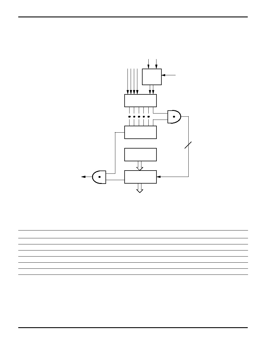
Interrupts. The Z8 has six different interrupts from six dif-
ferent sources. The interrupts are maskable and prioritized
(Figure 22). The six sources are divided as follows; three
sources are claimed by Port 3 lines P33-P31, two by
counter/timers, and one by the DSP (Table 6). The Inter-
rupt Mask Register globally or individually enables or dis-
ables the six interrupt requests.
Figure 22. Interrupt Block Diagram
Table 6. Interrupt Types, Sources, and Vectors
Name
Source
Vector Location
Comments
IRQ0
/DAV0, P32, AN2
0, 1
External (P32), Programmable Rise or Fall Edge Triggered
IRQ1
/DAV1, P33
2, 3
External (P33), Fall Edge Triggered
IRQ2
/DAV2, P31, TIN, AN2
4, 5
External (P31), Programmable Rise or Fall Edge Triggered
IRQ3
IRQ3
6, 7
Internal (DSP activated), Fall Edge Triggered
IRQ4
T0
8, 9
Internal
IRQ5
TI
10, 11
Internal
Interrupt
Edge
Select
IRQ Register
(D6, D7)
IRQ1, 3, 4, 5
IRQ
IMR
IPR
Priority
Logic
6
Global
Interrupt
Enable
Vector Select
Interrupt
Request
IRQ0 IRQ2

Z89138/Z89139
Voice Processing Controllers
Zilog
34
P R E L I M I N A R Y
DS97TAD0201
Z8 FUNCTIONAL DESCRIPTION (Continued)
When more than one interrupt is pending, priorities are re-
solved by a programmable priority encoder controlled by
the Interrupt Priority Register. An interrupt machine cycle
is activated when an interrupt request is granted. This dis-
ables all subsequent interrupts, pushes the Program
Counter and Status Flags to the stack, and then branches
to the program memory vector location reserved for that in-
terrupt.
All Z8 interrupts are vectored through locations in the pro-
gram memory. This memory location and the next byte
contain the 16-bit address of the interrupt service routine
for that particular interrupt request. To accommodate
polled interrupt systems, interrupt inputs are masked and
the Interrupt Request Register can be polled to determine
which of the interrupt requests needs service.
An interrupt resulting from AN1 is mapped into IRQ2, and
an interrupt from AN2 is mapped into IRQ0. Interrupts
IRQ2 and IRQ0 can be rising, falling or both edge trig-
gered, and are programmable by the user. The software
can poll to identify the state of the pin.
Programming bits for the Interrupt Edge Select are located
in the IRQ Register (R250), bits D7 and D6 . The configu-
ration is shown in Table 7.
Clock. The Z89138/139 on-chip oscillator has a high-gain,
parallel-resonant amplifier for connection to a crystal, LC,
ceramic resonator, or any suitable external clock source
(XTAL1 = Input, XTAL2 = Output). The crystal should be
AT cut, 20.48 MHz maximum, with a series resistance
(RS) less than or equal to 100 Ohms. The system clock
(SCLK) is one half the crystal frequency.
The crystal is connected across XTAL1 and XTAL2 using
capacitors from each pin to Ground (Figure 23).
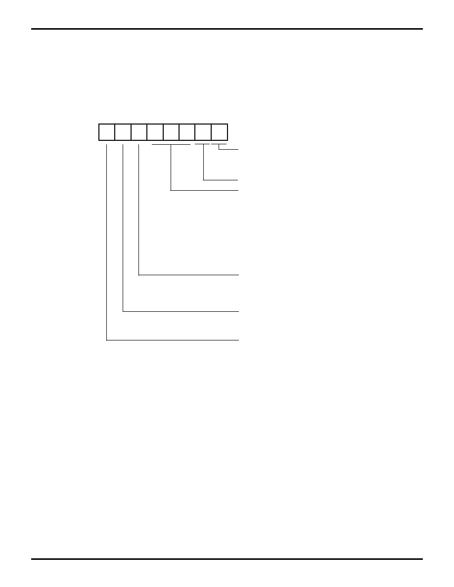
Table 7. IRQ Register
IRQ
Interrupt Edge
D7
D6
P31
P32
0
0
F
F
0
1
F
R
1
0
R
F
1
1
R/F
R/F
Notes:
F = Falling Edge
R = Rising Edge
Figure 23. Oscillator Configuration
XTAL1
XTAL2
C1
C2
C1
C2
XTAL1
XTAL2
XTAL1
XTAL2
Ceramic Resonator or
Crystal
LC
External Clock
L
Z89138/Z89139
Zilog
Voice Processing Controllers
DS97TAD0201
P R E L I M I N A R Y
35
1
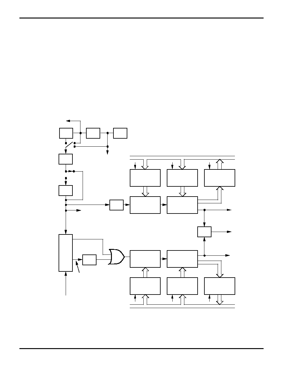
Counter/Timers. There are two 8-bit programmable
counter/timers (T1,T0), each driven by its own 6-bit pro-
grammable prescaler. The T1 prescaler is driven by inter-
nal or external clock sources. However, the T0 prescaler is
driven by the internal clock only (Figure 24).
The 6-bit prescalers can divide the input frequency of the
clock source by any integer number from 1 to 64. Each
prescaler drives its counter, which decrements the value
(0 to 256) that has been loaded into the counter. When the
counter reaches the end of the count, a timer interrupt re-
quest, IRQ4 (T0) or IRQ5 (T1), is generated.
The counters can be programmed to start, stop, restart to
continue, or restart from the initial value. The counters can
also be programmed to stop upon reaching zero (single
pass mode) or to automatically reload the initial value and
continue counting (modulo-n continuous mode).
The counters, but not the prescalers, are read at any time
without disturbing their value or count mode. The clock
source for T1 is user-definable and is either the internal mi-
croprocessor clock divided by four, or an external signal in-
put via Port 31. The Timer Mode register configures the ex-
ternal timer input (P31) as an external clock, a trigger input
that can be retriggerable or non-retriggerable, or as a gate
input for the internal clock. The counter/timers can be cas-
caded by connecting the T0 output to the input of T1.
Figure 24. Counter/Timer Block Diagram
PRE0
Initial Value
Register
T0
Initial Value
Register
T0
Current Value
Register
6-Bit
Down
Counter
8-bit
Down
Counter
˜
16
˜
4
6-Bit
Down
Counter
8-Bit
Down
Counter
PRE1
Initial Value
Register
T1
Initial Value
Register
T1
Current Value
Register
Clock
Logic
IRQ4
T
P36
OUT
IRQ5
Internal Data Bus
Write
Write
Read
Internal Clock
Gated Clock
Triggered Clock
TIN P31
Write
Write
Read
Internal Data Bus
External Clock
Internal
Clock
D0,D1
(SMR)
˜
4
˜
2
˜
2
˜
2
˜
2
OSC
T0, T2, T3
DSP Clock
D7, D6
(F) OC
(DSP CON)

Z89138/Z89139
Voice Processing Controllers
Zilog
36
P R E L I M I N A R Y
DS97TAD0201
Z8 FUNCTIONAL DESCRIPTION (Continued)
Port Configuration Register (PCON). The PCON regis-
ter configures the comparator output on Port 3. The PCON
register (Figure 25) is located in the Expanded Register
File at Bank F, location 00H.
Comparator Output Port 3 (D0). Bit 0 controls the com-
parator use in Port 3. A 1 in this location brings the com-
parator outputs to P34 and P35, and a 0 releases the Port
to its standard I/O configuration.
Port 4 and 5 Configuration Register (P45CON). The
P45CON register configures Port 4 and Port 5, individual-
ly, to open-drain or push-pull active. This register is located
in the Expanded Register File at Bank F, location 06H.
Port 4 Open-Drain (D0). Port 4 can be configured as an
open-drain by resetting this bit (D0 = 0) or configured as
push-pull active by setting this bit (D0 = 1). The default val-
ue is 1.
Port 5 Open-Drain (D4). Port 5 can be configured as an
open-drain by resetting this bit (D4 = 0) or configured as
push-pull active by setting this bit (D4 = 1). The default val-
ue is 1.
Power-On Reset (POR). A timer circuit clocked by a ded-
icated on-board RC oscillator is used for the Power-On Re-
set (POR) timer function. The POR time allows VCC and
the oscillator circuit to stabilize before instruction execu-
tion begins.
The POR timer circuit is a one-shot timer triggered by one
of three conditions:
1.
Power fail to Power OK status;
2.
Stop-Mode Recovery (if D5 of SMR=1);
3.
WDT time-out.
The POR time is a nominal 5 ms. Bit 5 of the STOP Mode
register determines whether the POR timer is bypassed af-
ter Stop-Mode Recovery (typical for external clock, RC/LC
oscillators).
HALT. HALT turns off the internal CPU clock, but not the
XTAL oscillation. The counter/timers and external inter-
rupts IRQ0, IRQ1, IRQ2, and IRQ3 remain active. The de-
vices are recovered by interrupts, either externally or inter-
nally generated.
STOP. This instruction turns off the internal clock and ex-
ternal crystal oscillation. It reduces the standby current to
20
µ
A or less. The STOP Mode is terminated by a reset
only, either by WDT time-out, POR, SMR, or external re-
set. This causes the processor to restart the application
program at address 000CH. In order to enter STOP (or
HALT) Mode, it is necessary to first flush the instruction
pipeline to avoid suspending execution in mid-instruction.
To do this, the user must execute a NOP (opcode=FFH)
immediately before the appropriate Sleep instruction. For
example:,
Figure 25. Port Configuration Register (PCON)
D7 D6
D5
D4
D3
D2
D1 D0
PCON (F) %00
R Always "1"
W 0 P34,P37 Standard output
1 P34,P37 Comparator output
R Always "1"
W No effect
Note: Reset condition is 11111110
FF
NOP
; clear the pipeline
6F
STOP
; enter STOP Mode
or
FF
NOP
; clear the pipeline
7F
HALT
; enter HALT Mode
Z89138/Z89139
Zilog
Voice Processing Controllers
DS97TAD0201
P R E L I M I N A R Y
37
1
Stop-Mode Recovery Register (SMR). This register se-
lects the clock divide value and determines the mode of
Stop-Mode Recovery (Figure 26). All bits are Write-Only
except bit 7, which is Read-Only. Bit 7 is a flag bit that is
hardware set on the condition of STOP recovery and reset
by a power-on cycle. Bit 6 controls whether a low level or
a high level is required from the recovery source. Bit 5 con-
trols the reset delay after recovery. Bits 2, 3, and 4, or the
SMR register, specify the source of the Stop-Mode Recov-
ery signal. Bits 0 and 1 determine the time-out period of the
WDT. The SMR is located in Bank F of the Expanded Reg-
ister group at address 0BH.
Figure 26. Stop-Mode Recovery Register (SMR)
D7
D6
D5
D4
D3
D2
D1
D0
SMR (FH) 0BH
W Stop Delay
0 OFF
1 ON*
R Always "1"
W 0 Low Stop Recovery Level*
1 High Stop Recovery Level
R Always "1"
W No effect
R 0 POR*
1 Stop-Mode Recovery
*
Default Setting After Reset
Reset After Stop-Mode Recovery
W 000 POR only*
001 No effect
010 P31
011 P32
100 P33
101 Half second timeout from
33 kHz ext. osc.
110 P2 NOR 0-3
111 P2 NOR 0-7
R Always "1"
W 0 SCLK/TCLK not divided by 16
1 SCLK/TCLK divided by 16
R Always "1"
Reserved

Z89138/Z89139
Voice Processing Controllers
Zilog
38
P R E L I M I N A R Y
DS97TAD0201
Z8 FUNCTIONAL DESCRIPTION (Continued)
SCLK/TCLK divide-by-16 Select (D0). D0 of the SMR
controls a divide-by-16 prescaler of SCLK/TCLK. The pur-
pose of this control is to selectively reduce device power
consumption during normal processor execution (SCLK
control) and/or HALT Mode (where TCLK sources
counter/timers and interrupt logic).
Stop-Mode Recovery Source (D4-D2). These three bits
of the SMR specify the wake-up source of the Stop-Mode
Recovery (Figure 27 and Table 8).
Stop-Mode Recovery Delay Select (D5). When Low, this
bit disables the 5 ms /RESET delay after Stop-Mode Re-
covery. The default configuration of this bit is 1. If the "fast"
wake up is selected, the Stop-Mode Recovery source is
kept active for at least 5 TpC.
Stop-Mode Recovery Edge Select (D6). A 1 in this bit po-
sition indicates that a high level on any one of the recovery
sources wakes the Z89138/139 from STOP Mode. A 0 in-
dicates low level recovery. The default is 0 on POR (Table
8).
Cold or Warm Start (D7). This bit is set by the device
upon entering STOP Mode. It is active High, and is 0 (cold)
on POR/WDT /RESET. This bit is Read-Only. It is used to
distinguish between a cold or warm start.
Figure 27. Stop-Mode Recovery Source
P31
P32
P33
HSEC
Stop Mode Recovery Edge
Select (SMR)
P33 From Pads
Digital/Analog Mode
Select (P3M)
To P33 Data
Latch and IRQ1
To POR
RESET
SMR
D4 D3 D2
0 0 0
VDD
SMR
SMR
SMR
SMR
SMR
D4 D3 D2
0 1 0
0 1 1
D4 D3 D2
1 0 0
D4 D3 D2
1 0 1
D4 D3 D2
1 1 0
D4 D3 D2
1 1 1
P20
P23
P20
P27
MUX
Table 8. Stop-Mode Recovery Source
SMR:432
Operation
Description of Action
D4
D3
D2
0
0
0
POR and/or external reset recovery
0
0
1
No effect
0
1
0
P31 transition
0
1
1
P32 transition
1
0
0
P33 transition
1
0
1
HSEC
1
1
0
Logical NOR of P20 through P23
1
1
1
Logical NOR of P20 through P27
Z89138/Z89139
Zilog
Voice Processing Controllers
DS97TAD0201
P R E L I M I N A R Y
39
1
DSP Control Register (DSPCON). The DSPCON register
controls various aspects of the Z8 and the DSP. It can con-
figure the internal system clock (SCLK) or the Z8, /RE-
SET, and HALT of the DSP, and control the interrupt inter-
face between the Z8 and the DSP (Table 9).
Z8 IRQ3 (D0). When read, this bit indicates the status of
the Z8 IRQ3. The Z8 IRQ3 is set by the DSP by writing to
D9 of DSP External Register 4 (ICR). By writing a 1 to this
bit, Z8 IRQ3 is Reset.
DSP INT2 (D1). This bit is linked to DSP INT2. Writing a 1
to this bit sets the DSP INT2. Reading this bit indicates the
status of the DSP INT2.
DSP RUN (D4). This bit defines the HALT Mode of the
DSP. If this bit is set to 0, then the DSP clock is turned off
to minimize power consumption. After this bit is set to 1,
then the DSP will continue code execution from where it
was halted. After a hardware reset, this bit is reset to 1.
DSP RESET (D5). Setting this bit to 1 will reset the DSP.
If the DSP was in HALT Mode, this bit is automatically pre-
set to 1. Writing a 0 has no effect.
Z8 SCLK (D7-D6). These bits define the SCLK frequency
of the Z8. The oscillator can be divided by 8, 4, or 2. After
a reset, both bits default to 00.
Table 9. DSP Control Register (F) OCH [Read/Write]
Field
DSPCON (F)0CH
Position
Attrib
Value
Label
Z8_SCLK
76------
R/W
00
01
1x
(OSC/8)
(OSC/4)
(OSC/2)
DSP_Reset
--5-----
R
Return "0"
W
0
No effect
1
Reset DSP
DSP_Run
---4----
R/W
0
Halt_DSP
1
Run_DSP
Reserved
----32--
W
No effect
R
Return "0"
No effect
DSP_INT2
------1-
R
FB_DSP_INT2
W
1
Set DSP_INT2
0
No effect
Z8_IRQ3
-------0
R
FB_Z8_IRQ3
W
1
Clear IRQ3
0
No effect
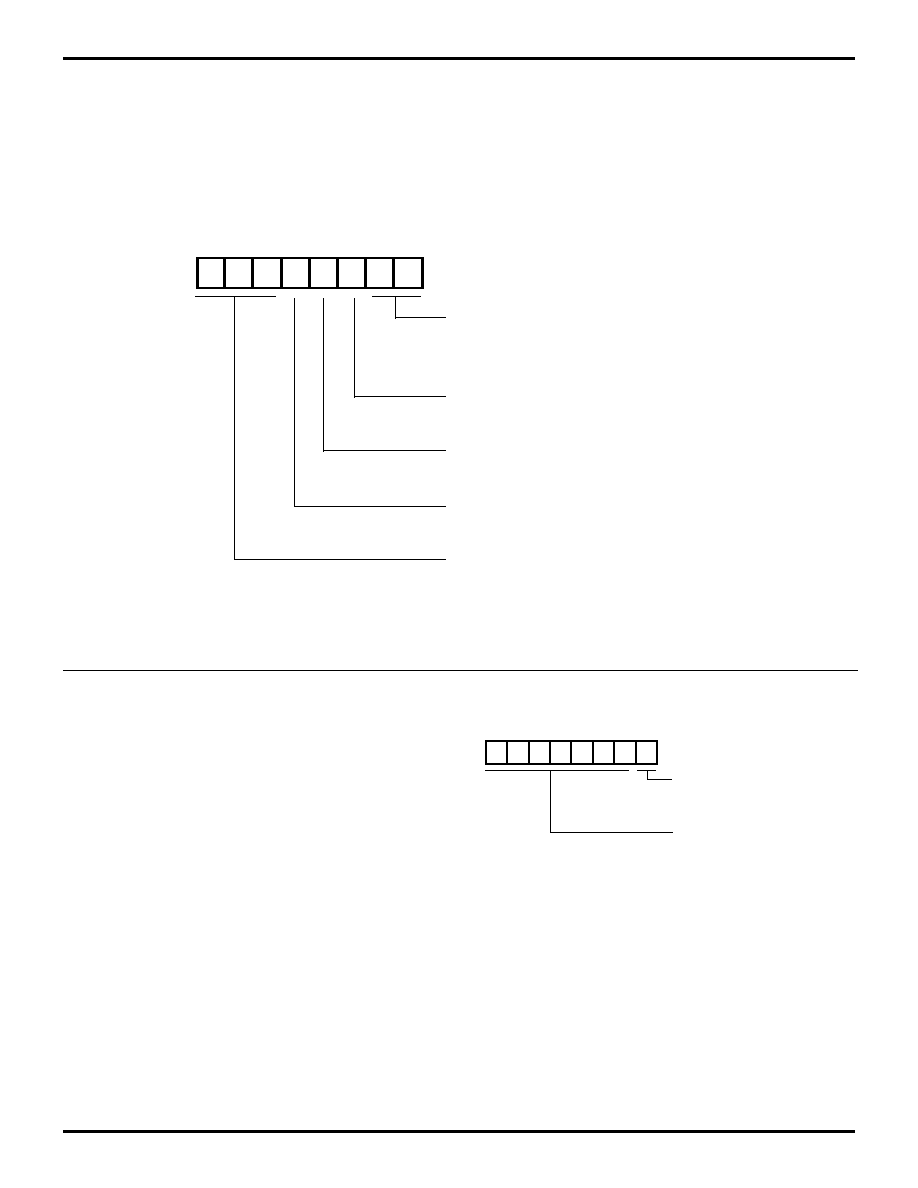
Z89138/Z89139
Voice Processing Controllers
Zilog
40
P R E L I M I N A R Y
DS97TAD0201
Z8 FUNCTIONAL DESCRIPTION (Continued)
Watch-Dog Timer Mode Register (WDTMR). The WDT
is a retriggerable one-shot timer that resets the Z8 if it
reaches its terminal count. The WDT is initially enabled by
executing the WDT instruction and refreshed on subse-
quent executions of the WDT instruction. The WDT circuit
is driven by an on-board RC oscillator or external oscillator
from the XTAL1 pin. The POR clock source is selected
with bit 4 of the WDT register (Figure 28). The WDTMR
register is accessible only within 64 Z8 clock cycles after
POR.
Half-Second Timer Status Register (HSEC). The half-
second timer status register (Figure 29) is a free-running
timer clocked by the external 32.768 kHz crystal. In normal
operation mode, every half-second, the timer will time-out
and set bit 0 (D0) of the HSEC register to 1. The user can
reset this bit for real timing. In Stop mode, this timer can be
used as a Stop-Mode Recovery source. Every half-sec-
ond, the timer will recover the Stop mode and bit 0 of the
HSEC register will be set to 1. Therefore, in STOP Mode,
the user can keep real time.
Figure 28. Watch-Dog Timer Mode Register
D7 D6 D5 D4 D3 D2
D1 D0
WDTMR (F) 0F
WDT TAP INT RC OSC EXTERNAL CLOCK
00 5 ms 256 Tpc
01* 15 ms 512 Tpc
10 25 ms 1024 Tpc
11 100 ms 4096 Tpc
WDT During HALT
0 OFF
1 ON*
WDT During STOP
0 OFF
1 ON*
XTAL1/INT RC Select for WDT
0 On-Board RC
1 XTAL
W No effect
R Always "1"
* Default setting after RESET
Figure 29. Half-Second Timer Status Register
D7 D6 D5 D4 D3 D2
D1 D0
HSEC (F) 0E
R 1 Half second time-out
0 No time-out
W 1 No effect
0 RESET the half second timer bit
Reserved R "0"
W No effect

Z89138/Z89139
Zilog
Voice Processing Controllers
DS97TAD0201
P R E L I M I N A R Y
41
1
WDT Time Select (D0, D1). These bits selects the WDT
time period. The configuration is shown in Table 10.
WDT During HALT (D2). This bit determines whether or
not the WDT is active during HALT Mode. A 1 indicates ac-
tive during HALT. The default is 1.
WDT During STOP (D3). This bit determines whether or
not the WDT is active during STOP Mode. Since XTAL
clock is stopped during STOP Mode, the on-board RC
must be selected as the clock source to the POR counter.
A 1 indicates active during STOP. The default is 1.
Clock Source for WDT (D4). This bit determines which
oscillator source is used to clock the internal POR and
WDT counter chain. If the bit is a 1, the internal RC oscil-
lator is bypassed and the POR and WDT clock source is
driven from the external pin, XTAL1. The default configu-
ration of this bit is 0 which selects the RC oscillator.
Table 10. WDT Time Select
Time-out of
Time-out of
D1
D0`
Internal RC OSC
XTAL Clock
0
0
5 ms min
256 TpC
0
1
15 ms min
512 TpC
1
0
25 ms min
1024 TpC
1
1
100 ms min
4096 TpC
Notes:
TpC = XTAL clock cycle.
Tolerance =
±
10%
Figure 30. Resets and WDT
CLK
18 Clock RESET
Generator
RESET
Clear
WDT TAP SELECT
RC
OSC.
CK
CLR
5 ms POR
5 ms 15 ms 25 ms 100 ms
2V Operating
Voltage Det.
Internal
RESET
WDT Select
(WDTMR)
CK Source
Select
(WDTMR)
XTAL
VDD
2V REF.
From Stop
Mode
Recovery
Source
WDT
Stop Delay
Select (SMR)
12 ns Glitch Filter
+
-
4 Clock
Filter
WDT/POR Counter Chain
M
U
X
/RESET

Z89138/Z89139
Voice Processing Controllers
Zilog
42
P R E L I M I N A R Y
DS97TAD0201
DSP REGISTERS DESCRIPTION
General. The DSP is a high-performance second genera-
tion CMOS Digital Signal Processor with a modified Har-
vard-type architecture with separate program and data
ports. The design has been optimized for processing pow-
er and saving silicon space.
Registers. The DSP has eight internal registers and sev-
en external registers. The external registers are for the A/D
and D/A converters, and the mailbox and interrupt interfac-
ing between DSP to the Z8. External registers are access-
ed in one machine cycle, the same as internal registers.
DSP Registers
There are 15 internal and extended 16-bit registers which
are defined in Table 11.
EXT3-EXT0 (External Registers 3-0). These are the Mail-
box Registers used by the DSP and Z8 to communicate.
These four 16-bit registers correspond to the eight outgo-
ing and eight incoming 8-bit registers in Bank B of the Z8's
Expanded Register File.
EXT4 (DSP Interrupt Control Register (ICR)). This register
controls the interrupts in the DSP as well as the interrupts
in common between the DSP and the Z8. It is accessible
by the DSP only, except for bit F and bit 9.
EXT5 (D/A and A/D Data Register). This register is used
by both D/A and A/D converters. The D/A converter is
loaded by writing to this register, while the A/D converter is
addressed by reading from this register. The Register
EXT5 is accessible only by the DSP.
EXT6 (Analog Control Register). This register controls the
D/A and A/D converters. It is a read/write register accessi-
ble only by the DSP.
Table 11. DSP Registers
Register
Attribute
Register Definition
BUS
Read
Data-Bus
X
Read/Write
X Multiplier Input, 16-Bit
Y
Read/Write
Y Multiplier Input, 16-Bit
A
Read/Write
Accumulator, 24-Bit
SR
Read/Write
Status Register
SP
Read/Write
Stack Pointer
PC
Read/Write
Program Counter
P
Read
Output of MAC, 24-Bit
EXT0
Read
Z8 ERF Bank B, Register 00-01 (from Z8)
Write
Z8 ERF Bank B, Register 08-09 (to Z8)
EXT1
Read
Z8 ERF Bank B, Register 02-03 (from Z8)
Write
Z8 ERF Bank B, Register 0A-0B (to Z8)
EXT2
Read
Z8 ERF Bank B, Register 04-05 (from Z8)
Write
Z8 ERF Bank B, Register 0C-0D (to Z8)
EXT3
Read
Z8 ERF Bank B, Register 06-07 (from Z8)
Write
Z8 ERF Bank B, Register 0E-0F (to Z8)
EXT4
Read/Write
DSP Interrupt Control Register
EXT5
Read A/D
Converter
Write
D/A Converter
EXT6
Read/Write
Analog Control Register
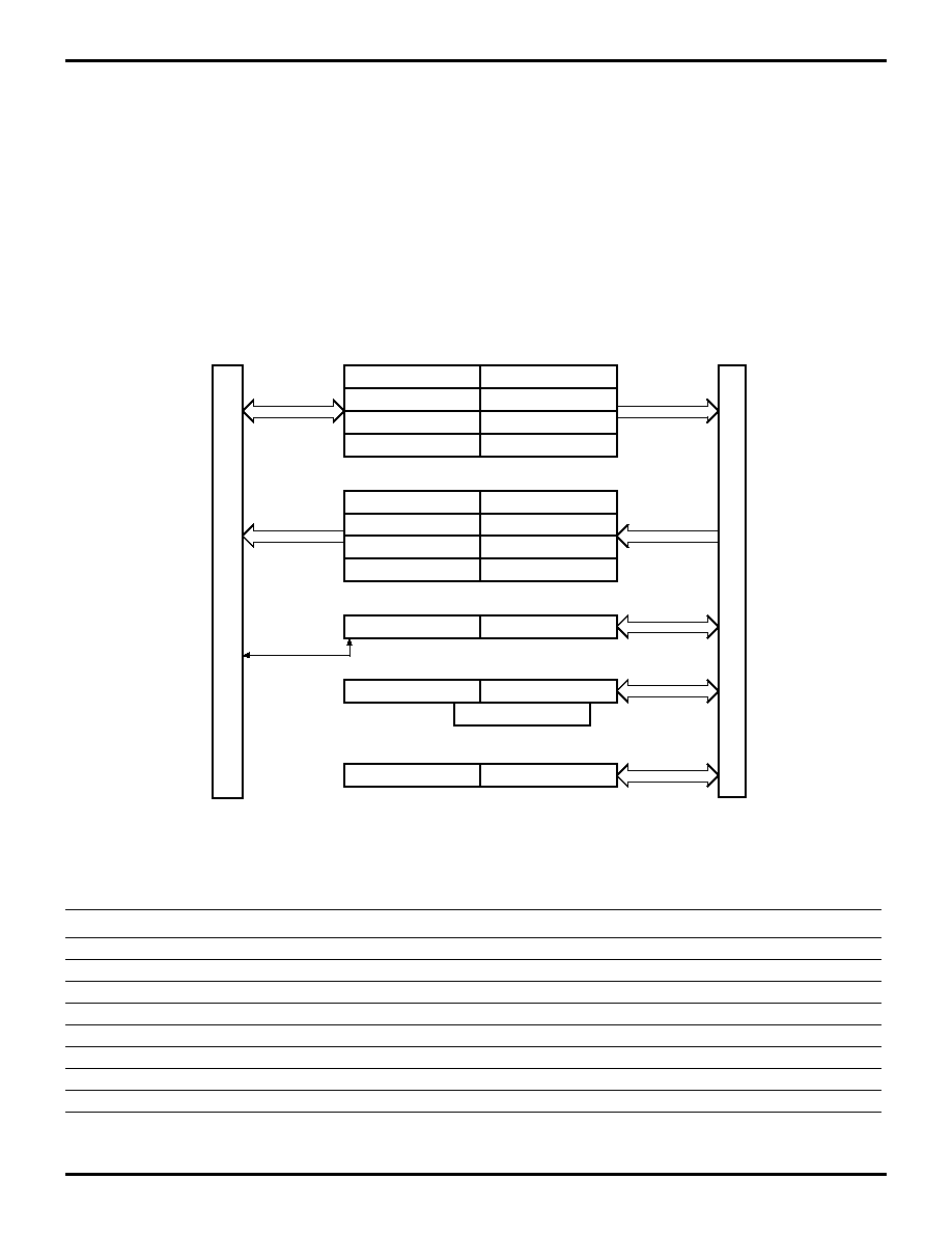
Z89138/Z89139
Zilog
Voice Processing Controllers
DS97TAD0201
P R E L I M I N A R Y
43
1
DSP Z8 Mail Box
To receive information from the DSP, the Z8 uses eight in-
coming registers which are mapped in the Z8 extended
Register File (Bank B, 08 to 0F). The DSP treats these as
four 16-bit registers that correspond to the eight incoming
Z8 registers (Figure 31).
The Z8 can supply the DSP with data through eight outgo-
ing registers mapped into both the Z8 Expanded Register
File (Bank B, Registers 00 to 07) and the external register
interface of the DSP. These registers are Read/Write and
can be used as general-purpose registers of the Z8. The
DSP can only read information from these registers. Since
the DSP uses a 16-bit data format and the Z8 an 8-bit data
format, eight outgoing registers of the Z8 correspond to
four DSP registers. The DSP can only read information
from the outgoing registers.
Both the outgoing registers and the incoming registers
share the same DSP address (EXT3-EXT0).
Note: The Z8 can read and write to ERF Bank B R00-R07,
Registers 08-0F are Read-Only from the Z8.
Figure 31. Z8-DSP Interface
Outgoing Registers
Incoming Registers
DSP Interrupt Control Register
D/A and A/D Data Registers
Analog Control Register
(B)00, (B)01
(B)02, (B)03
(B)04, (B)05
(B)06, (B)07
(B)08, (B)09
(B)0A, (B)0B
(B)0C, (B)0D
(B)0E, (B)0F
(F)0C
EXT0
EXT2
EXT0
EXT2
EXT4
EXT1
EXT3
EXT1
EXT3
EXT5
EXT6
D7, D1
Z8 Data Bus
DSP
Data Bus
D9
D2
Table 12. Z8 Outgoing Registers (Read-Only from DSP)
Field
Position
Attrib
Value
Label
Outgoing [0] (B)00
76543210
R/W
%NN
(B)00/DSP_ext0_hi
Outgoing [1] (B)01
76543210
R/W
%NN
(B)01/DSP_ext0_lo
Outgoing [2] (B)02
76543210
R/W
%NN
(B)02/DSP_ext1_hi
Outgoing [3] (B)03
76543210
R/W
%NN
(B)03/DSP_ext1_lo
Outgoing [4] (B)04
76543210
R/W
%NN
(B)04/DSP_ext2_hi
Outgoing [5] (B)05
76543210
R/W
%NN
(B)05/DSP_ext2_lo
Outgoing [6] (B)06
76543210
R/W
%NN
(B)06/DSP_ext3_hi
Outgoing [7] (B)07
76543210
R/W
%NN
(B)07/DSP_ext3_lo

Z89138/Z89139
Voice Processing Controllers
Zilog
44
P R E L I M I N A R Y
DS97TAD0201
DSP REGISTERS DESCRIPTION (Continued)
Table 13. Z8 Incoming Registers (Write-Only from DSP)
Field
Position
Attrib
Value
Label
Incoming [8] (B)08
76543210
R
%NN
DSP_ext0_hi
W
No Effect
Incoming [9] (B)09
76543210
R
%NN
DSP_ext0_lo
W
No Effect
Incoming [a] (B)0A
76543210
R
%NN
DSP_ext1_hi
W
No Effect
Incoming [b] (B)0B
76543210
R
%NN
DSP_ext1_lo
W
No Effect
Incoming [c] (B)0C
76543210
R
%NN
DSP_ext2_hi
W
No Effect
Incoming [d] (B)0D
76543210
R
%NN
DSP_ext2_lo
W
No Effect
Incoming [e] (B)0E
76543210
R
%NN
DSP_ext3_hi
W
No Effect
Incoming [f] (B)0F
76543210
R
%NN
DSP_ext3_lo
W
No Effect
Table 14. DSP Incoming Registers
Field
Position
Attrib
Value
Label
DSP_ext0
fedcba9876543210
R
%NNNN
(B)00, (B)01
Mail Box
W
(B)08, (B)09
DSP_ext1
fedcba9876543210
R
%NNNN
(B)02, (B)03
Mail Box
W
(B)0A, (B)0B
DSP_ext2
fedcba9876543210
R
%NNNN
(B)04, (B)05
Mail Box
W
(B)0C, (B)0D
DSP_ext3
fedcba9876543210
R
%NNNN
(B)06, (B)07
Mail Box
W
(B)0E, (B)0F
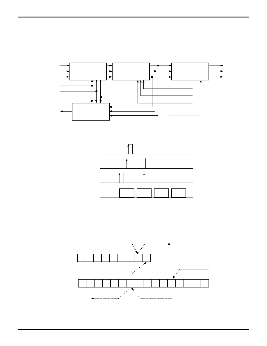
Z89138/Z89139
Zilog
Voice Processing Controllers
DS97TAD0201
P R E L I M I N A R Y
45
1
DSP Interrupts
The DSP processor has three interrupt sources (INT2,
INT1, INT0) (Figure 32). These sources have different pri-
ority levels (Figure 33). The highest priority, the next lower
and the lowest priority level are assigned to INT2, INT1
and INT0, respectively (Figure 34). The DSP does not al-
low interrupt nesting (interrupting service routines that are
currently being executed). When two interrupt requests oc-
cur simultaneously the DSP starts servicing the interrupt
with the highest priority level.
Figure 32. DSP Interrupts
Interrupt Priority Logic
Interrupt Request Logic
Interrupt Mask Logic
FeedBack Z8_INT MPX
Z8_INT
A/D INT
D/A INT
IPR2
IPR1
IPR0
FB DSP
CLEAR_INT1
CLEAR_INT2
CLEAR_INT0
ENABLE_INT
INT2
INT1
INT0
INT2
INT1
INT0
Figure 33. DSP Interrupt Priority Structure
INT0
INT1
INT2
DSP Execution
INT2
INT0
INT1
INT2
Figure 34. Interprocessor Interrupts Structure
4
9
After serving IRQ3,
set D0 to clear the
interrupt request.
The DSP sets D9 to
interrupt Z8 via Z8 IRQ3.
IRQ3 of the Z8
DSP INT2
After serving INT2,
set D4 to clear the
interrupt request.
On the Z8, set D1 to
interrupt DSP via DSP INT2.
DSP Side
Z8 Side
1
0
DSP CON
ICR
(EXT4)
Z89138/Z89139
Voice Processing Controllers
Zilog
46
P R E L I M I N A R Y
DS97TAD0201
DSP REGISTERS DESCRIPTION (Continued)
Table 15. EXT4 DSP Interrupt Control Register (ICR) Definition
Field
Position
Attrib
Value
Label
DSP_IRQ2
f---------------
R
1
Set_IRQ2
0
Reset_IRQ2
f---------------
W
No effect
DSP_IRQ1
-e--------------
R
1
Set_IRQ1
0
Reset_IRQ1
-e--------------
W
No effect
DSP_IRQ0
--d-------------
R
1
Set_IRQ0
0
Reset_IRQ0
--d-------------
W
No effect
DSP_MaskINT2
---c------------
R/W
1
Enable_INT2
0
Disable_INT2
DSP_MaskINT1
----b-----------
R/W
1
Enable_INT1
0
Disable_INT1
DSP_MaskINT0
-----a----------
R/W
1
Enable_INT0
0
Disable_INT0
Z8_IRQ3
------9---------
R
Return "0"
------9---------
W
1
Set_Z8_IRQ3
0
Reset_Z8_IRQ3
DSPintEnable
-------8--------
R/W
1
Enable
0
Disable
DSP_IPR2
--------7-------
R/W
Binary
IPR2
DSP_IPR1
---------6------
R/W
Binary
IPR1
DSP_IPR0
----------5-----
R/W
Binary
IPR0
Clear_IRQ2
-----------4----
R
Return "0"
-----------4----
W
1
Clear_IRQ2
0
Has_no_effect
Clear_IRQ1
------------3---
R
Return "0"
------------3---
W
1
Clear_IRQ1
0
No effect
Clear_IRQ0
-------------2--
R
Return "0"
-------------2--
W
1
Clear_IRQ0
0
No effect
Reserved
--------------10
W
No effect "0"
R

Z89138/Z89139
Zilog
Voice Processing Controllers
DS97TAD0201
P R E L I M I N A R Y
47
1
Interrupt Control Register (ICR). The ICR is mapped into
EXT4 of the DSP (Table 15). The bits are defined as fol-
lows:
DSP_IRQ2 (Z8 Interrupt). This bit is read by both Z8 and
DSP and is set only by writing to the Z8 expanded Register
File (Bank F, ROC, bit 0). This bit asserts IRQ2 of the DSP
and is cleared by writing to the Clear_IRQ2 bit.
DSP_IRQ1 (A/D Interrupt). This bit is read by the DSP only
and is set when valid data is present at the A/D output reg-
ister (conversion done). This bit asserts IRQ1 of the DSP
and is cleared by writing to the Clear_IRQ1bit.
DSP_IRQ0 (D/A Interrupt). This bit is read by DSP only
and is set by Timer3. This bit assists IRQ0 of the DSP and
is cleared by writing to the Clear_IRQ0 bit.
DSP_MaskIntX. These bits are accessed by the DSP
only. Writing a 1 to these locations allows the INT to be
serviced, while writing a 0 masks off the corresponding
INT.
Z8_IRQ3. This bit can be read by both the Z8 and the DSP
but can only be set by the DSP. Addressing this location
accesses bit D3 of the Z8 IRQ register, hence, this bit is
not implemented in the ICR. During the interrupt service
routine executed on the Z8 side, the User must reset the
Z8_IRQ3 bit by writing a 1 to bit D0 of the DSPCON.
The hardware of the Z89138/139 automatically resets
Z8_IRQ3 bit three instructions of the Z8 after 1 is written to
its location in register bank 0F. This delay provides the tim-
ing synchronization between the Z8 and the DSP sides
during interrupts. In summary, the interrupt service routine
of the Z8 for IRQ3 should be finished by:
LD ;
RP,#%0F
OR
;
r12,#%01
POP
;
RP
IRET
;
DSP Enable_INT. Writing a 1 to this location enables glo-
bal interrupts of the DSP while writing 0 disables them. A
system Reset globally disables all interrupts.
DSP_IPRX. This three-bit group defines the Interrupt Se-
lection logic as shown in Table 16.
Clear_IRQX. These bits are accessed by the DSP only.
Writing a 1 to these locations resets the corresponding
DSP_IRQX bits to 0. Clear_IRQX are virtual bits and are
not implemented.
Table 16. DSP Interrupt Selection
DSP_IPR[2-0]
2 1 0
Z8_INT is
switched to
A/D_INT is
switched to
D/A_INT is
switched to
0 0 0
INT2
INT1
INT0
0 0 1
INT1
INT2
INT0
0 1 0
INT2
INT0
INT1
0 1 1
INT1
INT0
INT2
1 0 0
INT0
INT2
INT1
1 0 1
INT0
INT1
INT2
1 1 0
Reserved
Reserved
Reserved
1 1 1
Reserved
Reserved
Reserved

Z89138/Z89139
Voice Processing Controllers
Zilog
48
P R E L I M I N A R Y
DS97TAD0201
DSP Analog Data Registers
The D/A conversion is DSP driven by sending 10-bit data
to the EXT5 of the DSP. The six remaining bits of EXT5 are
not used (Figure 35).
A/D supplies 8-bit data to the DSP through the register
EXT5 of the DSP. From the 16 bits of EXT5, only bits 2
through 9 are used by the A/D (Figure 36). Bits 0 and 1 are
padded with zeroes.
Figure 35. EXT5 Register D/A Mode Definition
F
E
D
C
B
A
9
8
7
6
5
4
3
2
1
0
Reserved
10-Bit Data for D/A
(Write Only)
Reserved
Figure 36. EXT5 Register A/D Mode Definition
F
E
D
C
B
A
9
8
7
6
5
4
3
2
1
0
Reserved
8-Bit Data From A/D Converter
(Read Only)
Reserved

Z89138/Z89139
Zilog
Voice Processing Controllers
DS97TAD0201
P R E L I M I N A R Y
49
1
ANALOG CONTROL REGISTER (ACR)
The Analog Control register is mapped to register EXT6 of
the DSP (Table 17). This read/write register is accessible
by the DSP only.
The 16-bit field of EXT6 defines modes of both the A/D and
the D/A. The High Byte configures the D/A while the Low
Byte controls the A/D mode.
Table 17. EXT6 Analog Control Register (ACR)
Field
Position
Attrib
Value
Label
20.48
MHz
29.49
MHz*
MPX_DSP_INT0
f---------------
R/W
1
P26
0
Timer3
Reserved
-edcba----------
R
Return "0"
W
No effect
Reserved
------9---------
R
Return "1"
W
No effect
D/A_SamplingRate
-------8--------
R/W
0
16 kHz
8.04 kHz
1
10 kHz
9.6 kHz
DSP_port (DSP1,
DSP0)
--------76------
R/W
User-defined DSP
outputs
Enable A/D
----------5-----
R/W
1
A/D Enabled
0
A/D Disabled
ConversionDone
-----------4----
W
No effect
R
1
Done
0
Not Done
StartConversion
------------3---
R/W
1
Start
0
Wait Timer
Reserved
-------------2--
R
Return "0"
W
No effect
20/29 MHz Select
--------------1-
R/W
1
29.49 MHz*
0
20.48 MHz
A/D_SamplingRate
---------------0
R/W
1
16 kHz
16 kHz
0
8 kHz
9.6 kHz
Notes:
* Default value
Optional feature

Z89138/Z89139
Voice Processing Controllers
Zilog
50
P R E L I M I N A R Y
DS97TAD0201
DSP IRQ0. This bit defines the source of the DSP IRQ0 in-
terrupt.
D/A_Sampling Rate. This field defines the sampling rate
of the D/A output. It changes the period to Timer3 interrupt
and the maximum possible accuracy of the D/A Sampling
Rate (Table 18).
DSP0. DSP0 is a general-purpose output pin connected to
Bit 6. This bit has no special significance and can be used
to output data by writing to bit 6.
DSP1. DSP1 is a general-purpose output pin connected to
Bit 7. This bit has no special significance and can be used
to output data by writing to bit 7.
Enable A/D. Writing a 0 to this location disables the A/D
converter, a 1 will enable it. A hardware reset forces this
bit to 0.
Conversion Done. This Read-Only flag indicates that the
A/D conversion is complete. Upon reading EXT5 (A/D da-
ta), the Conversion Done flag is cleared.
Start A/D Conversion. Writing a 1 to this location immedi-
ately starts one conversion cycle. If this bit is reset to 0 the
input data is converted upon successive Timer2 time-outs.
A hardware reset forces this bit to 1.
A/D_Sampling Rate. This field defines the sampling rate
of the A/D. It changes the period of Timer2 interrupt (Table
19).
DSP TIMERS
Timer2 is a free running counter that divides the XTAL fre-
quency (20.48 MHz) to support different sampling rates for
the A/D converter. The sampling rate is defined by the An-
alog Control Register. Upon reaching the end of a count,
the timer generates an interrupt request to the DSP.
Analogous to Timer2, Timer3 generates the different sam-
pling rates for the D/A converter. Timer3 also generates an
interrupt request to the DSP upon reaching its final count
value (Figure 37).
Table 18. D/A Data Accuracy
D/A_Sampling Rate
Sampling Rate
Bit 8
20.48 MHz
29.49 MHz
0
16 kHz
8.04 kHz
1
10 kHz
9.6 kHz
Table 19. A/D Sampling Rate
A/D_Sampling Rate
Sampling Rate
Bit 0
20.48 MHz
29.49 MHz
1
16 kHz
16 kHz
0
8 kHz
9.6 kHz
Figure 37. Timer2 and Timer3
OSC
20.48 MHz
Timer2
8, 16 kHz
Timer3
16, 10 kHz
A/D
D/A
Timer2
16, 9.6 kHz
USC
29.49 MHz
Timer3
8.04, 9.6 kHz
A/D
D/A
Z89138/Z89139
Zilog
Voice Processing Controllers
DS97TAD0201
P R E L I M I N A R Y
51
1
Pulse Width Modulator (PWM)
The PWM supports two different sampling rates (10 and 16
kHz), according to the settings of bit 8 of the ACR. The out-
put of the PWM can be assigned to logic 1 only during the
active region (which is 4/5 of the output signal period). The
output will be at logic 0 for the rest of the time. An excep-
tion occurs in 10 kHz PWM, where the active region covers
the whole output signal period (Figure 39). The active re-
gion is divided into 1024 time slots. In each of these time
slots, the output can be set to logic 1 or logic 0.
In order to increase the effective sampling rate, the PWM
employs a special technique of distributing the "logic 1" pe-
riod over the active region.
The 10-bit PWM data is divided into two parts: the upper
five bits (High_Val) and the lower five bits (Low_Val). The
1024 time slots in the active region are divided into 32
equal groups, with 32 time slots in each group. The first
slot of each of the 32 groups represents Low_Val, while
High_Val is represented by the remaining 31 time slots in
each group.
For example, a value of %13a is loaded into PWM data
register EXT 5:
%13a = 01 0011 1010B = 314
High_Val = 01001B = 9
Low_Val = 11010B = 26
26 out of 32 groups will then have their first slots set to log-
ic 1. The remaining one slot in each group has nine time
slots set to logic 1.
For 10 kHz PWM, the effective output frequency is 10K x
32 = 320 kHz. Figure 40 illustrates the waveform by using
a 6-bit PWM data (3-bit High_Val and 3-bit Low_Val).
Figure 38. PWM Waveform (shaded area shows the active region)
10 kHz
16 kHz
250
µ
s
100
µ
s
Z89138/Z89139
Voice Processing Controllers
Zilog
52
P R E L I M I N A R Y
DS97TAD0201
Figure 39. PWM Waveform of the Active Region
(for a 6-bit PWM data)

Z89138/Z89139
Zilog
Voice Processing Controllers
DS97TAD0201
P R E L I M I N A R Y
53
1
A/D CONVERTER (ADC)
Analog to Digital Converter
The A/D converter is an 8-bit half flash converter which
uses two reference resistor ladders for its upper four bits
(MSBs) and lower four bits (LSBs) conversion (Figure 40).
Two reference voltage pins, VREF+ (High) and VREF-
(Low), are provided for external reference voltage sup-
plies. During the sampling period, the converter is auto-ze-
roed before starting the conversion time depending on the
external clock frequency and the selection of the A/D sam-
pling rate (Figure 40). The sampling rates are 10 or 16 kHz
(XTAL = 20.48 MHz) in order to provide oversampling. The
rates are software controlled by the ACR (DSP External
Register 6). Timer2 supports the ADC. The maximum con-
version time is 2
µ
s.
Conversion begins by writing to the appropriate bit in the
Analog Control Register (ACR). The start commands are
implemented in such a way as to begin a conversion at any
time. If a conversion is in progress and a new start com-
mand is received, then the conversion in progress is abort-
ed and a new conversion initiated. This allows the pro-
grammed values to be changed without affecting a
conversion in progress. The new values take effect only af-
ter a new start command is received.
The ADC can be disabled (for low power) or enabled by an
analog Control Register bit.
Though the ADC functions for a smaller input voltage and
voltage reference, the noise and offsets remain constant
over the specified electrical range. The errors of the con-
verter will increase and the conversion time can also take
slightly longer due to smaller input signals.
Figure 40. A/D Converter
4-Bit
Flash
AN IN
Sample
Auto Zero m
4-Bit
DAC
≠
+
4 MSB
4-Bit
Flash
Auto Zero
4 LSB
Latch 4 MSB
Latch 4 LSB
Bits 9-2 Register 12 of DSP

Z89138/Z89139
Voice Processing Controllers
Zilog
54
P R E L I M I N A R Y
DS97TAD0201
Figure 42 shows the input circuit of the ADC. When con-
version starts, the analog input voltage from the input is
connected to the MSB and LSB flash converter inputs as
shown in the Input Impedance CKT diagram. Shunting 31
parallel internal resistances of the analog switches and si-
multaneously charging 31 parallel 1 pF capacitors is equiv-
alent to a 400 Ohms input impedance in parallel with a 31
pF capacitor. Other input stray capacitance adds about 10
pF to the input load. Input source resistances up to 2 kO-
hms can be used under normal operating conditions with-
out any degradation of the input settling time. For larger in-
put source resistance, longer conversion cycle times can
be required to compensate the input settling time problem.
V
REF
is set using the V
REF
+ pin.
Figure 41. ADC Timing Diagram
SCLK
1
2
3
4
5
6
7
8
9
10
11
26
27
28
29
30
31
32
P32
Input Sample
A/D Result
DSP INT
DSP Write
Notes:
1. SCLK = 10 MHz (XTAL =
20.48 MHz)
1
Figure 42. Input Impedance of ADC
CMOS Switch
on Resistance
2 - 5 k
C Parasitic
R Source
V Ref
C .5 pF
V Ref
C .5 pF
V Ref
C .5 pF
31 CMOS Digital
Comparators
Z89138/Z89139
Zilog
Voice Processing Controllers
DS97TAD0201
P R E L I M I N A R Y
55
1
Z8 EXPANDED REGISTER FILE REGISTERS
Expanded Register Bank B
Figure 43. Outgoing Register to DSP EXT0
(High Byte) (B) 00H [Read/Write]
Figure 44. Outgoing Register to DSP EXT0
(Low Byte)
(B) 01H [Read/Write]
Figure 45. Outgoing Register to DSP EXT1
(High Byte)
(B) 02H [Read/Write]
Figure 46. Outgoing Register to DSP EXT1
(Low Byte)
(B) 03H [Read/Write]
D7 D6 D5 D4 D3 D2 D1 D0
(B) 00
DSP EXT0,
Bits D15-D8
D7 D6 D5 D4 D3 D2 D1 D0
(B) 01
DSP EXT0,
Bits D7-D0
D7 D6 D5 D4 D3 D2 D1 D0
(B) 02
DSP EXT1,
Bits D15-D8
D7 D6 D5 D4 D3 D2 D1 D0
(B) 03
DSP EXT1,
Bits D7-D0
Figure 47. Outgoing Register to DSP EXT2
(High Byte)
(B) 04H [Read/Write]
Figure 48. Outgoing Register to DSP EXT2
(Low Byte)
(B) 05H [Read/Write]
Figure 49. Outgoing Register to DSP EXT3
(High Byte)
(B) 06H [Read/Write]
D7 D6 D5 D4 D3 D2 D1 D0
(B) 04
DSP EXT2,
Bits D15-D8
D7 D6 D5 D4 D3 D2 D1 D0
(B) 05
DSP EXT2,
Bits D7-D0
D7 D6 D5 D4 D3 D2 D1 D0
(B) 06
DSP EXT3,
Bits D15-D8
Z89138/Z89139
Voice Processing Controllers
Zilog
56
P R E L I M I N A R Y
DS97TAD0201
Figure 50. Outgoing Register to DSP EXT3
(Low Byte)
(B) 07H [Read/Write]
Figure 51. Incoming Register from DSP EXT0
(High Byte)
(B) 08H [Read-Only]
Figure 52. Incoming Register from DSP EXT0
(Low Byte)
(B) 09H [Read-Only]
Figure 53. Incoming Register from DSP EXT1
(High Byte)
(B) 0AH [Read-Only]
D7 D6 D5 D4 D3 D2 D1 D0
(B) 07
DSP EXT3,
Bits D7-D0
D7 D6 D5 D4 D3 D2 D1 D0
(B) 08
DSP EXT0,
Bits D15-D8
D7 D6 D5 D4 D3 D2 D1 D0
(B) 09
DSP EXT0,
Bits D7-D0
D7 D6 D5 D4 D3 D2 D1 D0
(B) 0A
DSP EXT1,
Bits D15-D8
Figure 54. Incoming Register from DSP EXT1
(Low Byte)
(B) 0BH [Read-Only]
Figure 55. Incoming Register from DSP EXT2
(High Byte)
(B) 0CH [Read-Only]
Figure 56. Incoming Register from DSP EXT2
(Low Byte)
(B) 0DH [Read-Only]
Figure 57. Incoming Register from DSP EXT3
(High Byte)
(B) 0EH [Read-Only]
D7 D6 D5 D4 D3 D2 D1 D0
(B) 0B
DSP EXT1,
Bits D7-D0
D7 D6 D5 D4 D3 D2 D1 D0
(B) 0C
DSP EXT2,
Bits D15-D8
D7 D6 D5 D4 D3 D2 D1 D0
(B) 0D
DSP EXT2,
Bits D7-D0
D7 D6 D5 D4 D3 D2 D1 D0
(B) 0E
DSP EXT3,
Bits D15-D8

Z89138/Z89139
Zilog
Voice Processing Controllers
DS97TAD0201
P R E L I M I N A R Y
57
1
Expanded Register Bank F
Figure 58. Incoming Register from DSP EXT3
(Low Byte)
(B) 0FH [Read-Only]
Figure 59. Port Configuration Register (PCON)
(F) 00H [Write-Only]
Figure 60. Port 4 Data Register
(F) 02H [Read/Write]
Figure 61. Port 4 Mode Register
(F) 03H [Write-Only]
D7 D6 D5 D4 D3 D2 D1 D0
(B) 0F
DSP EXT3,
Bits D7-D0
D7 D6
D5
D4
D3
D2
D1 D0
PCON (F) %00
R Always "1"
W 0 P34,P37 Standard output
1 P34,P37 Comparator output
R Always "1"
W No effect
Note: Reset condition is 11111110
D7 D6 D5 D4 D3 D2 D1 D0
P4D (FH) 02H
Data
D7 D6 D5 D4 D3 D2 D1 D0
P40-P47 I/O Definition
0 Defines Bit as Output
1 Defines Bit as Input
Returns "FF" Upon Read
P4M (FH) 03H
Figure 62. Port 5 Data Register
(F) 04H [Read/Write]
Figure 63. Port 5 Mode Register
(F) 05H [Write-Only]
Figure 64. Port 4 and 5 Configuration Register
(F) 06H [Write-Only]
D7 D6 D5 D4 D3 D2 D1 D0
P5D (FH) 04H
Data
D7
D6
D5
D4
D3
D2
D1
D0
P5M (FH) 05H
P50-P57 I/O Definition
0 Defines Bit as Output
1 Defines Bit as Input*
Returns "FF" Upon Read
* Default setting after Reset
P45M (FH) 06H
(Write only)
Port 4 Configuration Bit
0 Open-Drain
1 Push-pull
No effect
Port 5 Configuration Bit
0 Open-Drain
1 Push-pull
No effect
D7 D6
D5
D4
D3
D2 D1
D0

Z89138/Z89139
Voice Processing Controllers
Zilog
58
P R E L I M I N A R Y
DS97TAD0201
Figure 65. Stop-Mode Recovery Register (SMR)
(F) 0BH [Read/Write]
D7
D6
D5
D4
D3
D2
D1
D0
SMR (FH) 0BH
W Stop Delay
0 OFF
1 ON*
R Always "1"
W 0 Low Stop Recovery Level*
1 High Stop Recovery Level
R Always "1"
W No effect
R 0 POR*
1 Stop-Mode Recovery
*
Default Setting After Reset
Reset After Stop-Mode Recovery
W 000 POR only*
001 No effect
010 P31
011 P32
100 P33
101 Half second timeout from
33 kHz ext. osc.
110 P2 NOR 0-3
111 P2 NOR 0-7
R Always "1"
W 0 SCLK/TCLK not divided by 16
1 SCLK/TCLK divided by 16
R Always "1"
Reserved
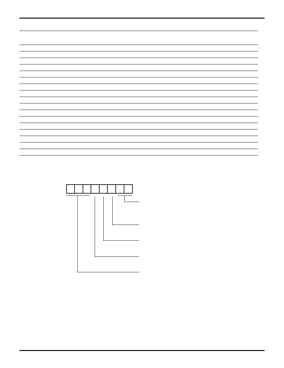
Z89138/Z89139
Zilog
Voice Processing Controllers
DS97TAD0201
P R E L I M I N A R Y
59
1
Table 20. DSP Control Register (F) 0CH [Read/Write]
Field
DSPCON (F) 0CH
Position
Attributes
Value
Label
Z8_SCLK
76------
R/W
00
OSC/8
01
OSC/4
1x
OSC/2
DSP_Reset
--5-----
R
Return "0"
W
0
No effect
1
Reset DSP
DSP_Run
---4----
R/W
0
Halt_DSP
1
Run_DSP
Reserved
----32--
xx
Return "0"
No effect
IntFeedback
------1-
R
FB_DSP_INT2
W
1
Set DSP_INT2
0
No effect
-------0
R
FB_Z8_IRQ3
W
1
Clear IRQ3
0
No effect
Figure 66. Watch-Dog Timer Mode Register
(F) 0FH [Read/Write]
D7 D6 D5 D4 D3 D2
D1 D0
WDTMR (F) 0F
WDT TAP INT RC OSC EXTERNAL CLOCK
00 5 ms 256 Tpc
01* 15 ms 512 Tpc
10 25 ms 1024 Tpc
11 100 ms 4096 Tpc
WDT During HALT
0 OFF
1 ON*
WDT During STOP
0 OFF
1 ON*
XTAL1/INT RC Select for WDT
0 On-Board RC
1 XTAL
W No effect
R Always "1"
* Default setting after RESET

Z89138/Z89139
Voice Processing Controllers
Zilog
60
P R E L I M I N A R Y
DS97TAD0201
Z8 CONTROL REGISTERS
Figure 67. Reserved (F0H)
Figure 68. Timer Mode Register
(F1H: Read/Write)
Figure 69. Counter/Timer 1 Register
(F2H: Read/Write)
D7
D6
D5
D4
D3
D2
D1
D0
RESERVED
R240
D7
D6
D5
D4
D3
D2
D1
D0
0 Disable T0 Count
1 Enable T0 Count
0 No Function
1 Load T0
0 No Function
1 Load T1
0 Disable T1 Count
1 Enable T1 Count
TIN Modes
00 External Clock Input
01 Gate Input
10 Trigger Input
(Non-retriggerable)
11 Trigger Input
(Retriggerable)
TOUT Modes
00 Not Used
01 T0 Out
10 T1 Out
11 Internal Clock Out (P36)
R241 TMR
D7
D6
D5 D4
D3
D2
D1
D0
T1 Low Byte Initial Value
(When Written)
T1 Low Byte Current Value
(When Read)
R242 T1
Figure 70. Prescaler 1 Register
(F3H: Write-Only)
Figure 71. Counter/Timer 0 Register
(F4H: Read/Write)
Figure 72. Prescaler 0 Register
(F5H: Write-Only)
D7
D6
D5
D4
D3
D2
D1
D0
Count Mode
0 T1 Single Pass
1 T1 Modulo N
Clock Source
1 T1Internal
0 T1External Timing Input
(TIN) Mode
Prescaler Modulo
(Range: 1-64 Decimal
01-00 HEX)
R243 PRE1
D7
D6
D5
D4 D3 D2
D1
D0
T0 Low Byte Initial Value
(When Written)
T0 Low Byte Current Value
(When Read)
R244 T0
D7 D6
D5
D4 D3
D2
D1
D0
Count Mode
0 T1 Single Pass
1 T1 Modulo N
Clock Source
1 T1Internal
0 T1External Timing Input
(TIN) Mode
Prescaler Modulo
(Range: 1-64 Decimal
01-00 HEX)
R243 PRE1
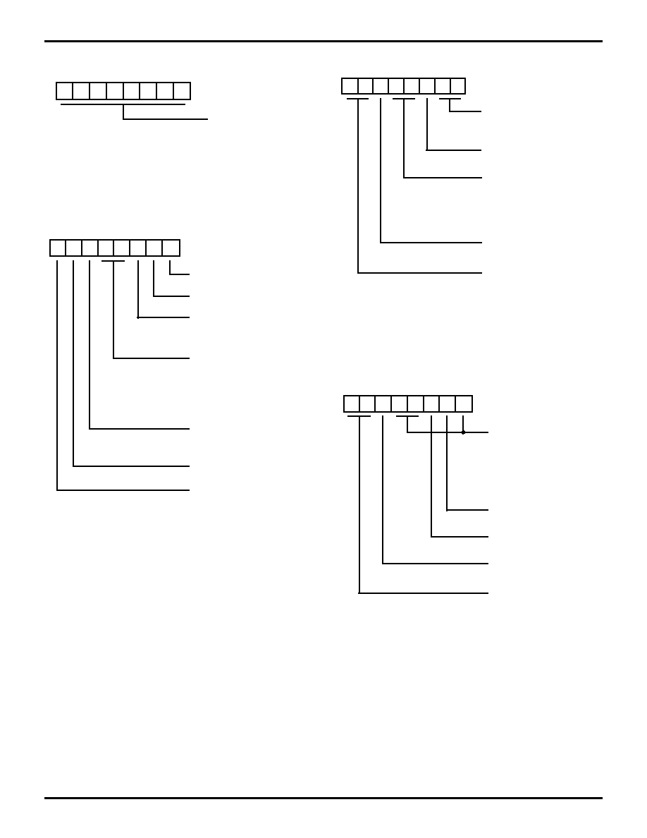
Z89138/Z89139
Zilog
Voice Processing Controllers
DS97TAD0201
P R E L I M I N A R Y
61
1
Figure 73. Port 2 Mode Register
(F6H: Write-Only)
Figure 74. Port 3 Mode Register
(F7H: Write-Only)
D7 D6
D5
D4
D3
D2
D1
D0
P20 - P27 I/O Definition
0 Defines Bit as Output
1 Defines Bit as Input
*
R246 P2M
*
Default Setting After Reset
*
Default Setting After Reset
D7
D6
D5
D4
D3
D2
D1
D0
R247 P3M
0 Port 2 Pull-Ups Open Drain
*
1 Port 2 Pull-Ups Active
0 P31, P32 Digital Mode
*
1 P31, P32 Analog Mode
0 P32 = Input
*
P35 = Output
*
1 P32 = /DAV0/RDY0
P35 = RDY0//DAV0
00 P33 = Input
*
P34 = Output
*
01 P33 = Input
P34 = /DM
10 P33 = Input
P34 = /DM
11 P33 = /DAV1/RDY1
P34 = RDY1//DAV1
0 P31 = Input (TIN)
*
P36 = Output (TOUT)
*
1 P31 = /DAV2/RDY2
P36 = RDY2//DAV2
0 P30 = Input
P37 = Output
Reserved
Figure 75. Port 0 Mode Register
(F8H: Write-Only)
Figure 76. Interrupt Priority Register
(F9H: Write-Only)
D7
D6
D5
D4
D3
D2
D1
D0
R248 P01M
P00 - P03 Mode
00 Output
01 Input
*
1X A11 - A8
Stack Selection
0 External
1 Internal
*
P10 - P17 Mode
00 Byte Output
01 Byte Input
*
10 AD7 - AD0
11 High-Impedance AD7 - AD0,
/AS, /DS, /R//W, A11 - A8,
A15 - A12, If Selected
P04 - P07 Mode
00 Output
01 Input
*
1X A15 - A12
External Memory Timing
0 Normal
*
1 Extended
*
Default Setting After Reset
D7
D6
D5
D4
D3
D2
D1
D0
Interrupt Group Priority
000 Reserved
001 C > A > B
010 A > B > C
011 A > C > B
100 B > C > A
101 C > B > A
110 B > A > C
111 Reserved
IRQ3, IRQ5 Priority (Group A)
0 IRQ5 > IRQ3
1 IRQ3 > IRQ5
IRQ0, IRQ2 Priority (Group B)
0 IRQ2 > IRQ0
1 IRQ0 > IRQ2
IRQ1, IRQ4 Priority (Group C)
0 IRQ1 > IRQ4
1 IRQ4 > IRQ1
Reserved
R249 IPR

Z89138/Z89139
Voice Processing Controllers
Zilog
62
P R E L I M I N A R Y
DS97TAD0201
Z8 CONTROL REGISTERS (Continued)
Figure 77. Interrupt Request Register
(FAH: Read/Write)
Figure 78. Interrupt Mask Register
(FBH: Read/Write)
Figure 79. Flag Register
(FCH: Read/Write)
D7
D6
D5
D4
D3
D2
D1
D0
R250 IRQ
Inter Edge
P31
P32
= 00
P31
P32
= 01
P31
P32
= 10
P31
P32
= 11
IRQ0 = P32 Input
IRQ1 = P33 Input
IRQ2 = P31 Input
IRQ3 = DSP
IRQ4 = T0
IRQ5 = T1
D7
D6
D5
D4
D3
D2
D1
D0
1 Enables RAM Protect
1 Enables IRQ0-IRQ5
(D0 = IRQ0)
1 Enables Interrupts
R251 IMR
D7
D6
D5
D4
D3
D2
D1
D0
R252 FLAGS
User Flag F1
User Flag F2
Half Carry Flag
Decimal Adjust Flag
Overflow Flag
Sign Flag
Zero Flag
Carry Flag
Figure 80. Register Pointer
(FDH: Read/Write)
Figure 81. Stack Pointer High
(FEH: Read/Write)
Figure 82. Stack Pointer Low
(FFH: Read/Write)
D7 D6
D5
D4
D3
D2
D1
D0
R253 RP
Expanded Register File Bank
Working Register Group
D7 D6
D5
D4
D3
D2
D1
D0
Stack Pointer Upper
Byte (SP8 - SP15)
R254 SPH
D7 D6
D5
D4 D3
D2
D1
D0
Stack Pointer Lower
Byte (SP0 - SP7)
R255 SPL

Z89138/Z89139
Zilog
Voice Processing Controllers
DS97TAD0201
P R E L I M I N A R Y
63
1
PACKAGE INFORMATION
Figure 83. 100-Pin QFP Package Diagram
Figure 84. 100-Pin VQFP Package Diagram
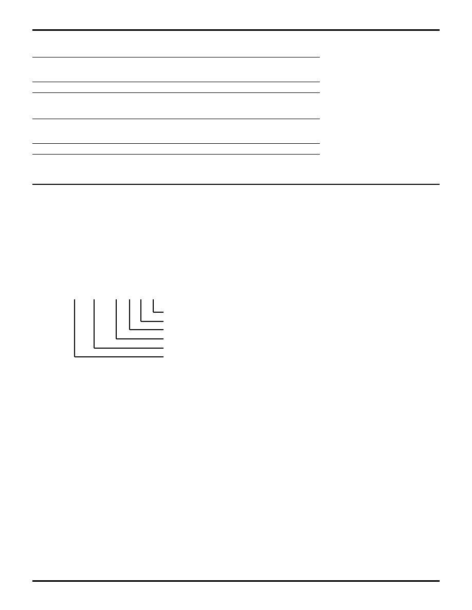
Z89138/Z89139
Voice Processing Controllers
Zilog
64
P R E L I M I N A R Y
DS97TAD0201
ORDERING INFORMATION
For fast results, contact your local Zilog sales office for assistance in ordering the part(s) desired.
CODES
Packages
F = Quad Flatpack (QFP)
A = Very Small Quad Flatpack (VQFP)
Temperature
S = 0
∞
C to + 55
∞
C
Speeds
20 = 20.48 MHz
29 = 29.49 MHz
Environmental
C = Plastic Standard
Z89138 (20 MHz)
Z89138 (29 MHz)
100-Pin QFP
100-Pin VQFP
100-Pin QFP
100-Pin VQFP
Z8913820FSC
Z8913820ASC
Z8913829FSC
Z8913829ASC
Z89139 (20 MHz)
Z89139 (29 MHz)
100-Pin QFP
100-Pin VQFP
100-Pin QFP
100-Pin VQFP
Z8913920FSC
Z8913920ASC
Z8913929FSC
Z8913929ASC
Example:
Z 89138 20 F S C
Environmental Flow
Temperature
Package
Speed
Product Number
Zilog Prefix
is a Z89138, 20.48 MHz, QFP, 0
∞
C to +55
∞
C, Plastic Standard Flow

Z89138/Z89139
Zilog
Voice Processing Controllers
DS97TAD0201
P R E L I M I N A R Y
65
1
© 1997 by Zilog, Inc. All rights reserved. No part of this
document may be copied or reproduced in any form or by
any means without the prior written consent of Zilog, Inc.
The information in this document is subject to change
without notice. Devices sold by Zilog, Inc. are covered by
warranty and patent indemnification provisions appearing
in Zilog, Inc. Terms and Conditions of Sale only. Zilog, Inc.
makes no warranty, express, statutory, implied or by
description, regarding the information set forth herein or
regarding the freedom of the described devices from
intellectual property infringement. Zilog, Inc. makes no
warranty of merchantability or fitness for any purpose.
Zilog, Inc. shall not be responsible for any errors that may
appear in this document. Zilog, Inc. makes no commitment
to update or keep current the information contained in this
document.
Zilog's products are not authorized for use as critical
components in life support devices or systems unless a
specific written agreement pertaining to such intended use
is executed between the customer and Zilog prior to use.
Life support devices or systems are those which are
intended for surgical implantation into the body, or which
sustains life whose failure to perform, when properly used
in accordance with instructions for use provided in the
labeling, can be reasonably expected to result in
significant injury to the user.
Zilog, Inc. 210 East Hacienda Ave.
Campbell, CA 95008-6600
Telephone (408) 370-8000
FAX 408 370-8056
Internet: http://www.zilog.com

Z89138/Z89139
Voice Processing Controllers
Zilog
66
P R E L I M I N A R Y
DS97TAD0201