 | –≠–ª–µ–∫—Ç—Ä–æ–Ω–Ω—ã–π –∫–æ–º–ø–æ–Ω–µ–Ω—Ç: Z89166 | –°–∫–∞—á–∞—Ç—å:  PDF PDF  ZIP ZIP |

1
Z89165/166/167/168/169
DTAD C
ONTROLLERS
Z
ILOG
CP96TAD0103
FEATURES
s
25 Expanded Register Files
s
47 Input/Output Lines (Z89165)
31 Input/Output Lines (Z89166)
43 Input/Output Lines (Core Processor)
s
Six Vectored, Prioritized Z8 Interrupts with
Programmable Polarity
s
Three Vectored, Prioritized DSP Interrupts with
Programmable Polarity
s
Two Analog Comparators
s
Two Programmable Z8 8-Bit Counter/Timers,
Each with Two 6-Bit Programmable Prescaler
s
Watch-Dog Timer /Power-On Reset
s
On-Chip Oscillator that Accepts a Crystal,
Ceramic Resonator, LC, RC, or External Clock Drive
s
RAM and ROM Protect, Low-EMI Option
C
USTOMER
P
ROCUREMENT
S
PECIFICATION
s
Part
Z8 ROM
Z8 RAM*
Speed
Number
(KBytes)
(KBytes)
(MHz)
Z89165
24
236
20
Z89166
ROMless
236
20
Z89167
24
236
24
Z89168
ROMless
236
24
Z89169
32
236
24
*General-Purpose
s
Part
DSP ROM
DSP RAM
Speed
Number
(Words)
(Words)
(MHz)
Z89165
6K
512
20
Z89166
6K
512
20
Z89167
8K
512
24
Z89168
8K
512
24
Z89169
8K
512
24
s
68- and 84-Pin PLCC Packages
s
4.5- to 5.5-Volt Operating Range
s
Low-Power Consumption (200 mW Typical)
s
0
∞
C to +70
∞
C Temperature Range
GENERAL DESCRIPTION
Zilog's Digital Voice Processor Controller family
combines a Z8
Æ
microcontroller and a DSP processor
on-chip for a cost-effective turnkey system in digital
telephone answering devices and other voice processing
applications.
The dual-processor architecture is loosely coupled by
mailbox registers and an interrupt system, enabling DSP or
Z8 programs to be directed by events in each other's
domain.
The Z8 microcontroller uses an expanded register file to
allow access to register-mapped peripheral and I/O
circuits for programming versatility.
The 16-bit DSP processor features a 24-bit ALU and
accumulator with single-cycle instructions, providing the
algorithm processing power necessary for telephone voice
quality.
Z89165/167/169
AND
Z89166/168 (ROM
LESS
)
E
NHANCED
D
UAL
-P
ROCESSOR
DTAD C
ONTROLLERS
The Z89165/166 devices offer a half-flash 8-bit A/D
converter with up to 128 kHz sample rate and a 10-bit
Pulse-Width modulator (PWM) D/A converter, eliminating
the need for an external CODEC.
The Z89167/168/169 devices feature a hardware ARAM
interface, as well as a dual-CODEC interface. A 10-bit
PWM D/A converter is also on-chip.
Notes:
All Signals with a preceding front slash, "/", are active Low, e.g.:
B//W (WORD is active Low); /B/W (BYTE is active Low, only).
Power connections follow conventional descriptions below:
Connection
Circuit
Device
Power
V
CC
V
DD
Ground
GND
V
SS
2
Z89165/166/167/168/169
DTAD C
ONTROLLERS
CP96TAD0103
Z
ILOG
GENERAL DESCRIPTION
(Continued)
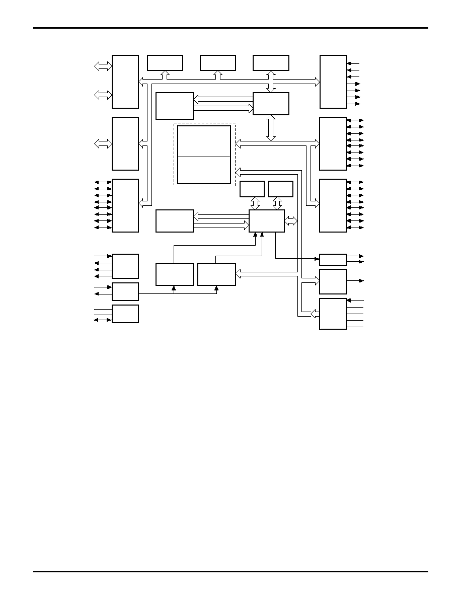
Port 0
P00
P01
P02
P03
P04
P05
P06
P07
P10
P11
P12
P13
P14
P15
P16
P17
P20
P21
P22
P23
P24
P25
P26
P27
P31
P32
P33
P40
P41
P42
P43
P44
P45
P46
P47
P50
P51
P52
P53
P54
P55
P56
P57
RMLS
/AS
/DS
R/W
Timer 0
Capture Reg.
Port 3
Port 1
Port 4
Port 2
Port 5
Timer 1
Register File
256 x 8 Bit
24 Kbytes
Program
ROM
(Z89165)
Z8 Core
Register Bus
Internal Address Bus
Internal Data Bus
Expanded Register
File
(Z8)
Peripheral
Register
(DSP)
Expanded
Register Bus
Extended Bus of the DSP
6K Words
Program
ROM
DSP Core
Internal Address Bus
Internal Data Bus
DSP Port
PWM
(10-Bit)
ADC
(8-Bit)
Timer 2
Timer 3
Extended Bus of the DSP
Ext.
Memory
Control
OSC
Power
XTAL1
XTAL2
VDD
GND
/RESET
INT 1
INT 2
DSP0
DSP1
AN IN
AN VDD
AN GND
VREF+
VREF-
PWM
256 Word
RAM 0
256 Word
RAM 1
P34
P35
P36
P37
Input
Output
I/O
(Bit
Programmable)
I/O
(Bit
Programmable)
Address
or I/O
(Nibble
Programmable)
Address/Data
or I/O
(Byte
Programmable)
I/O
(Bit
Programmable)
mailbox
Z89165/166 Functional Block Diagram
3
Z89165/166/167/168/169
DTAD C
ONTROLLERS
Z
ILOG
CP96TAD0103
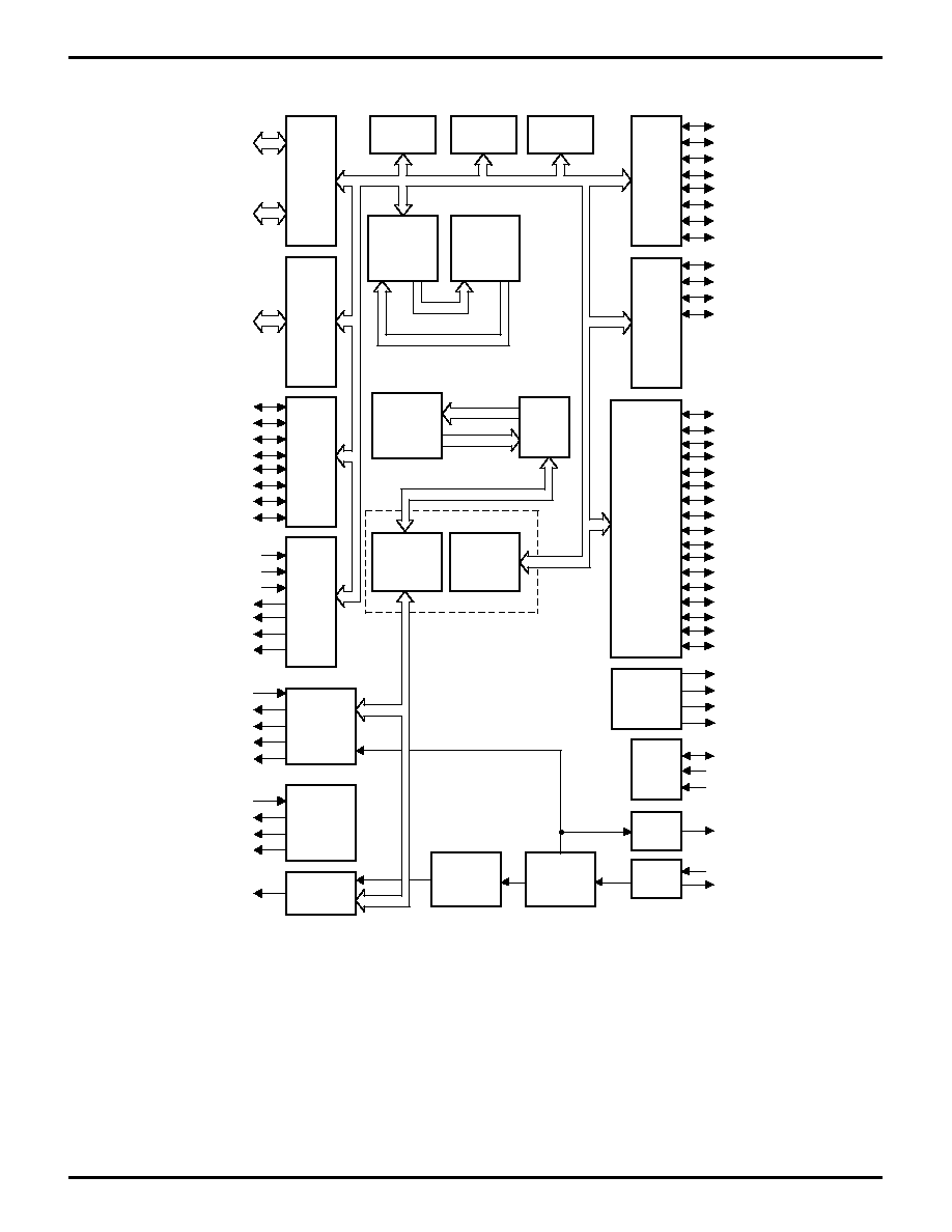
Port 0
P00
P01
P02
P03
P04
P05
P06
P07
P10
P11
P12
P13
P14
P15
P16
P17
P20
P21
P22
P23
P24
P25
P26
P27
P40
P41
P42
P43
P44
P45
P46
P47
P50
P51
P52
P53
Timer0
Port 4
Port 1
Port 5
Port 2
ARAM
Controller
Timer1
Register File
256 x 8-Bit
24 Kbytes (167)
32 Kbytes (169)
Program ROM
Z8 Core
Internal Register Bus
Timer3
Timer2
Power
ARAM
Control
I/O
(Bit
Programmable)
/RAS
/CAS
ARAM_R/W
ARAM_/OE
Address
or I/O
(Nibble
Programmable)
Address/Data
or I/O
(Byte
Programmable)
I/O
(Bit
Programmable)
DIN
DENA0
DCLK
DOUT
DENA1
PWM
(10-Bit)
Port 3
I/O
(Bit
Programmable)
Internal Address Bus
Internal Data Bus
8K Words
Program ROM
Address Bus
Data Bus
DSP
Core
Peripheral
Registers
(DSP)
Extended
Register File
(Z8)
Peripheral Data Bus of the DSP
Mailbox
Data0
Data1
Data2
Data3
ADDR0
ADDR1
ADDR2
ADDR3
ADDR4
ADDR5
ADDR6
ADDR7
ADDR8
ADDR9
ADDR10
ARAM_SEL0
ARAM_SEL1
Input
Output
P31
P32
P33
P34
P35
P36
P37
CODEC
Interface
RMLS
/AS
/DS
R/W
Z8 EXT.
Memory
Control
PWM
/RESET
VDD
GND
-5V
Control
Out -5V
OSC
XTAL1
XTAL2
GENERAL DESCRIPTION
(Continued)
Z89167/168/169 Functional Block Diagram
4
Z89165/166/167/168/169
DTAD C
ONTROLLERS
CP96TAD0103
Z
ILOG
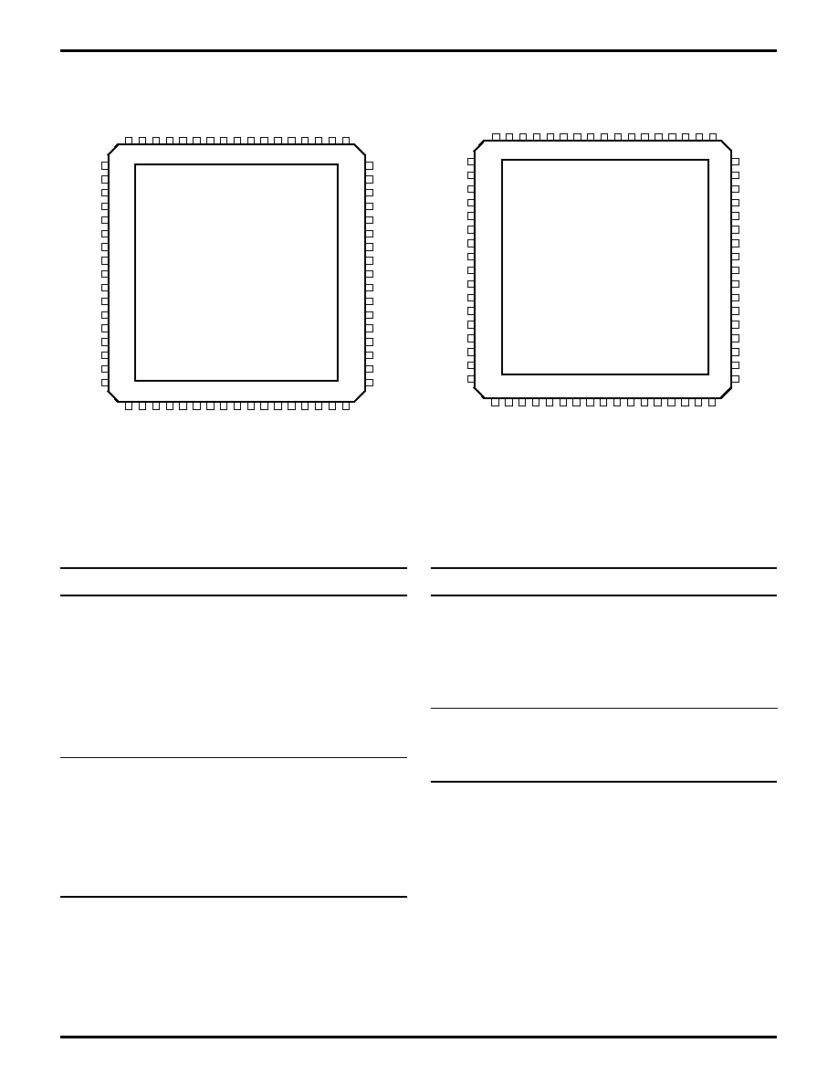
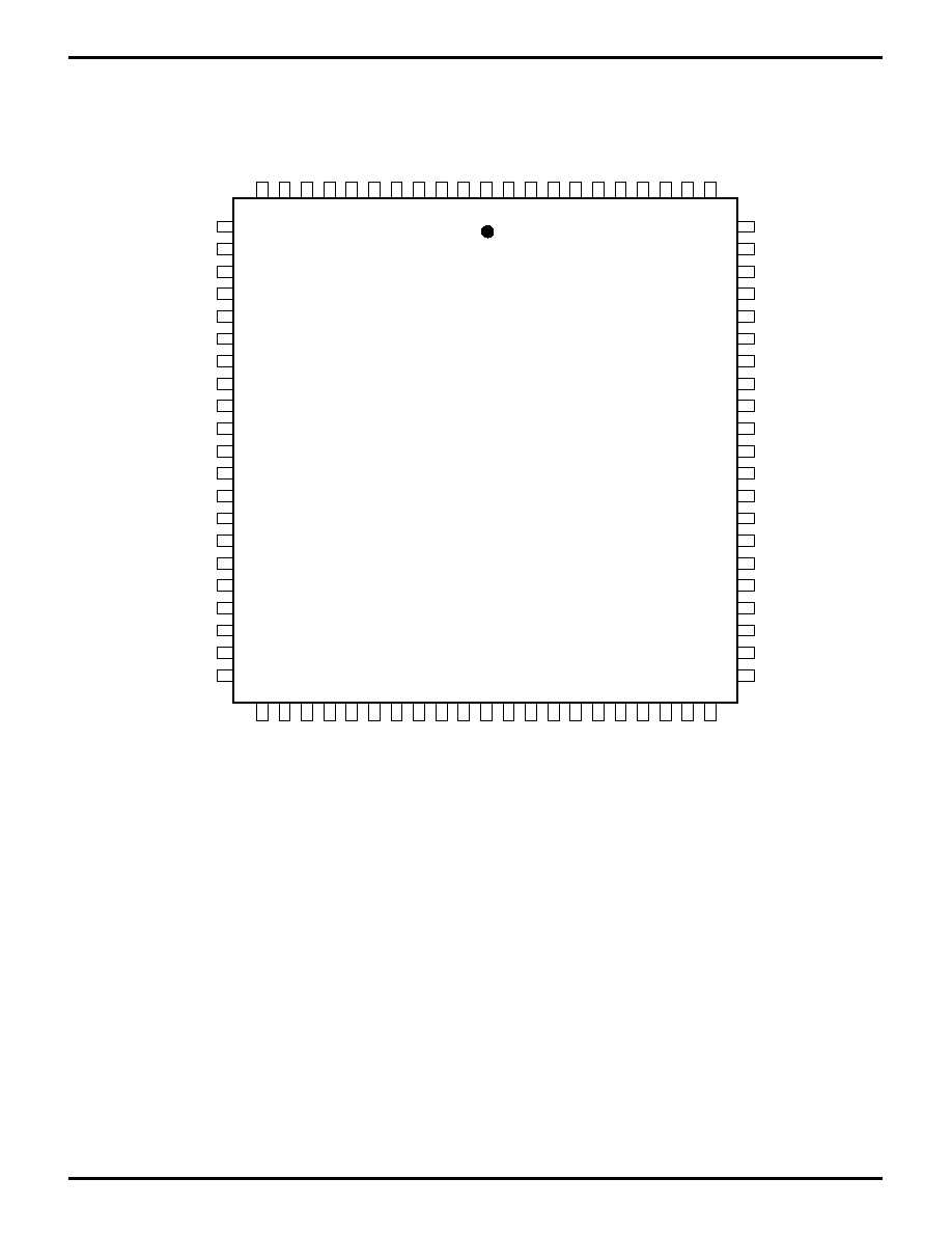
Z89165 68-Pin PLCC Pin Identification
Z89166 68-Pin PLCC Pin Identification
Pin Name
Function Direction
+5V
Power
5V Power Input
(Digital Power)
GND
Power
Device Ground
(Digital Ground)
AN
AIN
8-Bit A to D Converter Input
Vref≠
AIN
Low Reference Level for
A to D Converter
Vref+
AIN
High Reference Level for
A to D Converter
AN VDD
Power
ADC +5V Power
(Analog Power)
AN GND
Power
ADC Ground
(Analog Ground)
P00-P07 Data
I/O
General-Purpose I/O Port
P10-P17 Data
I/O
General-Purpose I/O Port
P20-P27 Data
I/O
General-Purpose I/O Port
Pin Identification
Pin Name
Function Direction
P31-P37 Data
I/O
General-Purpose I/O Port
P40-P47 Data
I/O
General-Purpose I/O Port
P50-P57 Data
I/O
General-Purpose I/O Port
DSP0-DSP1 Data 0
General-Purpose 0 Port
XTAL1
OSC1
20.48 MHz Crystal
Oscillator Input
XTAL2
OSC2
20.48 MHz Crystal
Oscillator Input
/RESET
I/O
System RESET
PWM
Out
10-Bit PWM, 5V TTL Output
Z89165
7
8
9
6
5
4
3
2
1
10
11
12
13
14
15
16
17
18
19
20
21
22
23
24
25
26
68 67 66 65 64 63 62 61
27 28 29 30 31 32 33 34 35 36 37 38 39 40 41 42 43
60
59
58
57
56
55
54
53
52
51
50
49
48
47
46
45
44
P31
P32
P33
P34
VDD
P35
P14
DSP1
DSP0
P36
P13
P37
P40
P12
P06
P41
P42
VREF+
ANIN
VREF-
ANGND
/AS
/RESET
R//W
PWM
P10
P47
P11
P46
P53
P45
P44
P43
N/C
XTAL2
XTAL1
P22
P56
P23
P55
P54
GND
P17
P05
P24
P16
P25
P15
P26
P27
N/C
P00
P01
P02
P03
P57
P50
P04
VDD
RMLS
/DS
P51
P52
P21
P20
P07
GND
ANVDD
PIN DESCRIPTION
Z89166
7
8
9
6
5
4
3
2
1
10
11
12
13
14
15
16
17
18
19
20
21
22
23
24
25
26
68 67 66 65 64 63 62 61
27 28 29 30 31 32 33 34 35 36 37 38 39 40 41 42 43
60
59
58
57
56
55
54
53
52
51
50
49
48
47
46
45
44
P31
P32
P33
P34
VDD
P35
P14
DSP1
DSP0
P36
P13
P37
P40
P12
P06
P41
P42
VREF+
ANIN
VREF-
ANGND
/AS
/RESET
R//W
PWM
P10
P47
P11
P46
P53
P45
P44
P43
/SYNC
XTAL2
XTAL1
P22
P56
P23
P55
P54
GND
P17
P05
P24
P16
P25
P15
P26
P27
SCLK
P00
P01
P02
P03
P57
P50
P04
VDD
VDD
/DS
P51
P52
P21
P20
P07
GND
ANVDD
5
Z89165/166/167/168/169
DTAD C
ONTROLLERS
Z
ILOG
CP96TAD0103
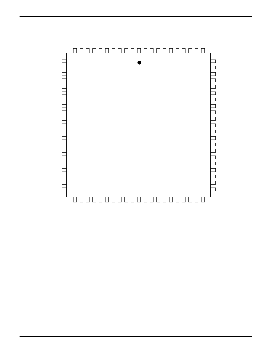
1 84
Z89168
84-Pin PLCC
33
42 43
32
53
54
11
12
75
74
VCC
ADDR0
ADDR1
ADDR2
ADDR4
ADDR5
ADDR6
ADDR7
ADDR8
ADDR9
ADDR10
ARAM_SEL0
ARAM_SEL1
DATA0
DATA1
DATA2
DATA3
/RAS
/CAS
GND
VCC
C_CLOCK
C_EN0
C_EN1
P50
P51
P52
P53
OUT_5V
GND
/AS
P37
P36
P35
P34
P33
P32
P31
PWM
P10
GND
P11
P12
P13
R/W
P14
P15
P16
P17
VCC
VCC
P00
P01
P02
P03
P04
P05
P06
P07
/RESET
ARAM_R/W
ARAM_OE
ADDR3
XT
AL1
XT
AL2
P27
P26
P24
P23
P22
P21
P20
/DS
P47
P46
P45
P44
P43
P42
P41
P40
C_DIN
C_DOU
T
P25
PIN DESCRIPTION
(Continued)
Z89168 84-Pin PLCC Pin Identification

6
Z89165/166/167/168/169
DTAD C
ONTROLLERS
CP96TAD0103
Z
ILOG
PIN DESCRIPTION
(Continued)
Z89168 84-Pin PLCC Pin Identification
I/O Port
Functions
Pin Number
I/O
Function
V
SS
32, 54, 65
Digital Ground
V
CC
12, 44, 74, 45
Digital VCC = +5 V
P00-P07
43-36
Input/Output
P00-P07 (General-purpose nibble programmable I/O port.)
P10-P17
55, 53-51, 49-46
Input/Output
P10-P17 (General-purpose byte programmable I/O port.)
P20-P27
2-9
Input/Output
P20-P27 (General-purpose bit programmable I/O.)
P31-P37
57-63
Input/Output
P31-P37 (General-purpose I/O port. Bits P31-P33 are inputs, while
bits P34-P37 are outputs.)
P40-P47
77-84
Input/Output
P40-P47 (General-purpose bit programmable I/O.)
P50-P53
70-67
Input/Output
P50-P53 (General-purpose bit programmable I/O.)
C_DIN
76
Input
Data input from CODEC.
C_DOUT
75
Output
Data output to CODEC.
C_CLOCK
73
Output
CODEC clock (2.048 MHz)
C_ENA0
72
Output
CODEC 0 enable (8 kHz)
C_ENA1
71
Output
CODEC 1 enable (8 kHz)
PWM
56
Output
Pulse Width Modulator output
DATA0
26
Input/Output
Data 0 I/O of the ARAM Interface
DATA1
27
Input/Output
Data 1 I/O of the ARAM Interface
DATA2
28
Input/Output
Data 2 I/O of the ARAM Interface
DATA3
29
Input/Output
Data 3 I/O of the ARAM Interface
ADDR0
13
Output
Address 0 line of the ARAM Interface
ADDR1
14
Output
Address 1 line of the ARAM Interface
ADDR2
15
Output
Address 2 line of the ARAM Interface
ADDR3
16
Output
Address 3 line of the ARAM Interface
ADDR4
17
Output
Address 4 line of the ARAM Interface
ADDR5
18
Output
Address 5 line of the ARAM Interface
ADDR6
19
Output
Address 6 line of the ARAM Interface
ADDR7
20
Output
Address 7 line of the ARAM Interface
ADDR8
21
Output
Address 8 line of the ARAM Interface
ADDR9
22
Output
Address 9 line of the ARAM Interface
ADDR10
23
Output
Address 10 line of the ARAM Interface for 4 Meg ARAMs. Select 2
output of ARAM Interface for 1 Meg ARAMs support. The latter
mode is used to switch between different pages of ARAM.
ARAM_SEL0
24
Output
Select 0 output of ARAM Interface. Used to switch between
different pages of ARAM.
ARAM_SEL1
25
Output
Select 1 output of ARAM Interface. Used to switch between
different pages of ARAM.
/RAS
30
Output
Row Address Strobe of ARAM Interface.
/CAS
31
Output
Column Address Strobe of ARAM Interface.
ARAM_R/W
34
Output
Read/Write Strobe of ARAM Interface.
ARAM_/OE
33
Output
Output Enable Strobe of ARAM Interface.
XTAL1
11
Input
24.57 MHz crystal input
XTAL2
10
Output
24.57 MHz crystal output
/Reset
35
Input
/RESET input
R/W
50
Output
Z8
Æ
external memory interface R/W output
/AS
64
Output
Z8 external memory interface /AS output
/DS
1
Output
Z8 external memory interface /DS output
7
Z89165/166/167/168/169
DTAD C
ONTROLLERS
Z
ILOG
CP96TAD0103
1 84
Z89C169/Z89C167
84-Pin PLCC
33
42 43
32
53
54
11
12
75
74
VCC
ADDR0
ADDR1
ADDR2
ADDR4
ADDR5
ADDR6
ADDR7
ADDR8
ADDR9
ADDR10
ARAM_SEL0
ARAM_SEL1
DATA0
DATA1
DATA2
DATA3
/RAS
/CAS
GND
VCC
C_CLOCK
C_EN0
C_EN1
P50
P51
P52
P53
OUT_5V
GND
/AS
P37
P36
P35
P34
P33
P32
P31
PWM
P10
GND
P11
P12
P13
R/W
P14
P15
P16
P17
RMLS
VCC
P00
P01
P02
P03
P04
P05
P06
P07
/RESET
ARAM_R/W
ARAM_OE
ADDR3
XT
AL1
XT
AL2
P27
P26
P24
P23
P22
P21
P20
/DS
P47
P46
P45
P44
P43
P42
P41
P40
C_DIN
C_DOU
T
P25
PIN DESCRIPTION
(Continued)
Z89167/169 84-Pin PLCC Pin Identification

8
Z89165/166/167/168/169
DTAD C
ONTROLLERS
CP96TAD0103
Z
ILOG
PIN DESCRIPTION
(Continued)
Z89169/Z89167 84-Pin PLCC, Pin Identification
I/O Port
Functions
Pin Number
I/O
Function
V
SS
32, 54, 65
Digital Ground
V
CC
12, 44, 74
Digital VCC = +5 V
P00-P07
43-36
Input/Output
P00-P07 (General-purpose nibble programmable I/O port.)
P10-P17
55, 53-51, 49-46
Input/Output
P10-P17 (General-purpose byte programmable I/O port.)
P20-P27
2-9
Input/Output
P20-P27 (General-purpose bit programmable I/O.)
P31-P37
57-63
Input/Output
P31-P37 (General-purpose I/O port. Bits P31-P33 are inputs, while
bits P34-P37 are outputs.)
P40-P47
77-84
Input/Output
P40-P47 (General-purpose bit programmable I/O.)
P50-P53
70-67
Input/Output
P50-P53 (General-purpose bit programmable I/O.)
C_DIN
76
Input
Data input from CODEC.
C_DOUT
75
Output
Data output to CODEC.
C_CLOCK
73
Output
CODEC clock (2.048 MHz)
C_ENA0
72
Output
CODEC 0 enable (8 kHz)
C_ENA1
71
Output
CODEC 1 enable (8 kHz)
PWM
56
Output
Pulse Width Modulator output
DATA0
26
Input/Output
Data 0 I/O of the ARAM Interface
DATA1
27
Input/Output
Data 1 I/O of the ARAM Interface
DATA2
28
Input/Output
Data 2 I/O of the ARAM Interface
DATA3
29
Input/Output
Data 3 I/O of the ARAM Interface
ADDR0
13
Output
Address 0 line of the ARAM Interface
ADDR1
14
Output
Address 1 line of the ARAM Interface
ADDR2
15
Output
Address 2 line of the ARAM Interface
ADDR3
16
Output
Address 3 line of the ARAM Interface
ADDR4
17
Output
Address 4 line of the ARAM Interface
ADDR5
18
Output
Address 5 line of the ARAM Interface
ADDR6
19
Output
Address 6 line of the ARAM Interface
ADDR7
20
Output
Address 7 line of the ARAM Interface
ADDR8
21
Output
Address 8 line of the ARAM Interface
ADDR9
22
Output
Address 9 line of the ARAM Interface
ADDR10
23
Output
Address 10 line of the ARAM Interface for 4 Meg ARAMs. Select 2
output of ARAM Interface for 1 Meg ARAMs support. The latter
mode is used to switch between different pages of ARAM.
ARAM_SEL0
24
Output
Select 0 output of ARAM Interface. Used to switch between
different pages of ARAM.
ARAM_SEL1
25
Output
Select 1 output of ARAM Interface. Used to switch between
different pages of ARAM.
/RAS
30
Output
Row Address Strobe of ARAM Interface.
/CAS
31
Output
Column Address Strobe of ARAM Interface.
ARAM_R/W
34
Output
Read/Write Strobe of ARAM Interface.
ARAM_/OE
33
Output
Output Enable Strobe of ARAM Interface.
XTAL1
11
Input
24.57 MHz crystal input
XTAL2
10
Output
24.57 MHz crystal output
ROMLESS
45
Input
Z8
Æ
Romless mode input (P0 and P1 are switched to D/A mode if
this pin is connected to VCC). Internally this pin is tight to GND.
/Reset
35
InputOutput
/RESET input/output
R/W
50
Output
Z8 external memory interface R/W output
/AS
64
Output
Z8 external memory interface /AS output
/DS
1
Output
Z8 external memory interface /DS output
9
Z89165/166/167/168/169
DTAD C
ONTROLLERS
Z
ILOG
CP96TAD0103
Notes:
*
Voltage on all pins with respect to GND.
See Ordering Information.
Symbol
Description
Min
Max
Units
V
CC
Supply Voltage (*)
≠0.3
+7.0
V
T
STG
Storage Temp
≠65
∞
+150
∞
C
T
A
Oper Ambient Temp
C
Power Dissipation
2.2
W
Stresses greater than those listed under Absolute Maxi-
mum Ratings may cause permanent damage to the de-
vice. This is a stress rating only; operation of the device at
any condition above those indicated in the operational
sections of these specifications is not implied. Exposure to
absolute maximum rating conditions for an extended
period may affect device reliability.
ABSOLUTE MAXIMUM RATINGS
STANDARD TEST CONDITIONS
The characteristics listed below apply for standard test
conditions as noted. All voltages are referenced to GND.
Positive current flows into the referenced pin (Test Load
Diagram).
+5V
From Output
Under Test
150 pF
9.1 k
2.1 k
Test Load Diagram
CAPACITANCE
T
A
= 25
∞
C, V
CC
= GND = 0V, f = 1.0 MHz, unmeasured pins to GND.
Parameter
Max
Input capacitance
12 pF
Output capacitance
12 pF
I/O capacitance
12 pF
DC ELECTRICAL CHARACTERISTICS
V
CC
T
A
= 0
∞
C to +70
∞
C
Typical
Sym
Parameter
Note [1]
Min
Max
@ 25
∞
C
Units
Notes
I
CC
Supply Current
5.0 V
65
40
mA
I
CC1
Halt Mode Current
5.0 V
20
6
mA
I
CC2
Stop Mode Current
[2]
Notes:
[1] 5.0V
±
0.5V.
[2] The typical Stop Mode Current value is 500
µ
A. The transient characteristics of the Stop Mode Current will vary according to the application and
should be validated in the specific application by the customer.

10
Z89165/166/167/168/169
DTAD C
ONTROLLERS
CP96TAD0103
Z
ILOG
DC ELECTRICAL CHARACTERISTICS
Z89165/Z89166
T
A
= 0
∞
C
Typical
V
CC
to +70
∞
@
Sym
Parameter
Note [1]
Min
Max
25
∞
C
Units
Conditions
V
MAX
Max Input Voltage
5.0V
7
V
I
IN
= 250
µ
A
V
CH
Clock Input High Voltage
5.0V
0.9 V
CC
V
CC
+0.3
2.5
V
Driven by External Clock Generator
V
CL
Clock Input Low Voltage
5.0V
GND-0.3
0.1 V
CC
1.5
V
Driven by External Clock Generator
V
IH
Input High Voltage
5.0V
0.7 V
CC
V
CC
+0.3
2.5
V
V
IL
Input Low Voltage
5.0V
GND-0.3
0.2 V
CC
1.5
V
V
OH
Output High Voltage
5.0V
V
CC
-0.4
4.8
V
I
OH
= -2.0 mA (Does not include XTAL2)
V
OL1
Output Low Voltage
5.0V
0.4
0.1
V
I
OH
= +4.0 mA
V
OL2
Output Low Voltage
5.0V
1.2
0.3
V
I
OL
= +12 mA, 3 Pin Max
(Does not include XTAL2)
V
RH
Reset Input High Voltage
5.0V
0.8 V
CC
V
CC
2.1
V
V
Rl
Reset Input Low Voltage
5.0V
GND-0.3
0.2 V
CC
1.7
V
V
OFFSET
Comparator Input Offset
5.0V
25
10
mV
Voltage
I
IL
Input Leakage
5.0V
-5
5
<5
µ
A
V
IN
= OV, V
CC
I
OL
Output Leakage
5.0V
-5
5
<5
µ
A
V
IN
= OV, V
CC
I
IR
Reset Input Current
5.0V
-55
-30
µ
A
Notes:
[1] 5.0
±
10% (V).

11
Z89165/166/167/168/169
DTAD C
ONTROLLERS
Z
ILOG
CP96TAD0103
Z891650A ADDITIONAL DC ELECTRICAL CHARACTERISTICS
1. A/D CONVERTER: ABSOLUTE INPUT CURRENT VALUES
S y m b o l
P a r a m e t e r
M a x i m u m
N o t e s
I
il
Anin
40
µ
A
I
ih
Anin
2
µ
A
I
input
Vref+
1.1 mA
With Vref≠ = 0V
Vref+ = 5.5V
80
µ
A
With Vref≠ = Vref+ Vref+ = 5.5V
I
input
Vref≠
1.1 mA
With Vref+ = 5.5V
Vref≠ = 0V
80
µ
A
With Vref+ = Vref+ Vref≠ = 0V
The following parameters should be verified on the ATE under
these conditions: 5.5V @ 25
∞
C.
2. OTHER PINS
Pin Under Test V a l u e
A d d i t i o n a l
C o n d i t i o n
Romless Pin
I
ih
(max) =
6
µ
A
No Reset
I
il
(max) =
6
µ
A
No Reset
I
ih
(max) =
1mA
During Reset
XTAL1
I
ih
(max) =
30
µ
A
While XTAL2 = 0V
No Reset
I
il
(max) =
30
µ
A
While XTAL2 = 5.5V
No Reset
XTAL2
I
ih
(max) =
10
µ
A
While XTAL1 = 0V
Stop Mode Invoked
I
il
(max) =
10
µ
A
While XTAL2 = 5V
Stop Mode Invoked
I
ih
(max) =
1 mA
While XTAL1 = 0V
No Reset
I
il
(max) =
1 mA
While XTAL2 = 5V
No Reset
I
ih
(max) =
4 mA
While XTAL1 = 0V
During Reset
I
il
(max) =
4 mA
While XTAL2 = 5V
During Reset
I
OL
(min) =
2 mA
V
OL
= 1V
V
DD
= 4.5V Temp = 70
∞
C
I
OH
(min) =
-1mA
V
OH
= V
DD
-1V
V
DD
= 4.5V Temp = 70
∞
C
I
OL
(max) =
7 mA
V
OL
= 1V
V
DD
= 5.5V Temp = 0
∞
C
I
OH
(max) =
6mA
V
OH
= V
DD
-1V
V
DD
= 5.5V Temp = 0
∞
C
P31, P32, P33
I
ih
(max) =
1
µ
A
(max) =
1
µ
A

12
Z89165/166/167/168/169
DTAD C
ONTROLLERS
CP96TAD0103
Z
ILOG
DC ELECTRICAL CHARACTERISTICS
Z89167/168/169
T
A
= 0
∞
C
to +70
∞
C
Typical
Units
Sym
Parameter
V
CC
Min
Max
25
∞
C
at
Conditions
Notes
Max Input Voltage
4.5V
7
V
I
IN
250 uA
5.5V
7
V
I
IN
250 uA
V
CH
Clock Input High Voltage
4.5V
0.9 V
CC
V
CC
+0.3
1.3
V
Driven by External Clock Generator
5.5V
0.9 V
CC
V
CC
+0.3
2.5
V
Driven by External Clock Generator
V
CL
Clock Input Low Voltage
4.5V
GND-0.3
0.1 V
CC
0.7
V
Driven by External Clock Generator
5.5V
GND-0.3
0.1 V
CC
1.5
V
Driven by External Clock Generator
V
IH
Input High Voltage
4.5V
0.7 V
CC
V
CC
+0.3
1.3
V
5.5V
0.7 V
CC
V
CC
+0.3
2.5
V
V
IL
Input Low Voltage
4.5V
GND-0.3
0.2 V
CC
0.7
V
5.5V
GND-0.3
0.2 V
CC
1.5
V
V
OH
Output High Voltge
4.5V
V
CC
-0.4
3.1
V
I
OH
= -2.0 mA
[1]
5.5V
V
CC
-0.4
4.8
V
I
OH
= -2.0 mA
V
OL1
Output Low Voltage
4.5V
0.6
0.2
V
I
OH
= +4.0 mA
5.5V
0.4
0.1
V
I
OL
= +4.0 mA
V
OL2
Output Low Voltage
4.5V
1.2
0.3
V
I
OL
= +6 mA, 3 Pin Max
5.5V
1.2
0.3
V
I
OL
= +12 mA, 3 Pin Max
V
RH
Reset Input High Voltage
4.5V
.8 V
CC
V
CC
1.5
V
5.5V
.8 V
CC
V
CC
2.1
V
V
Rl
Reset Input Low Voltage
4.5V
GND-0.3
0.2 V
CC
1.1
5.5V
GND-0.3
0.2 V
CC
1.7
V
OFFSET
Comparator Input Offset
4.5V
25
10
mV
Voltage
5.5V
25
10
mV
I
IL
Input Leakage
4.5V
-5
5
<5
µ
A
V
IN
= OV, V
CC
5.5V
-5
5
<5
µ
A
V
IN
= OV, V
CC
I
OL
Output Leakage
4.5V
-5
5
<5
µ
A
V
IN
= OV, V
CC
5.5V
-5
5
<5
µ
A
V
IN
= OV, V
CC
I
IR
Reset Input Current
4.5V
-45
-20
µ
A
5.5V
-55
-30
µ
A
Note:
[1] P10, P11 are measured at 4.5V only.
13
Z89165/166/167/168/169
DTAD C
ONTROLLERS
Z
ILOG
CP96TAD0103
AC CHARACTERISTICS
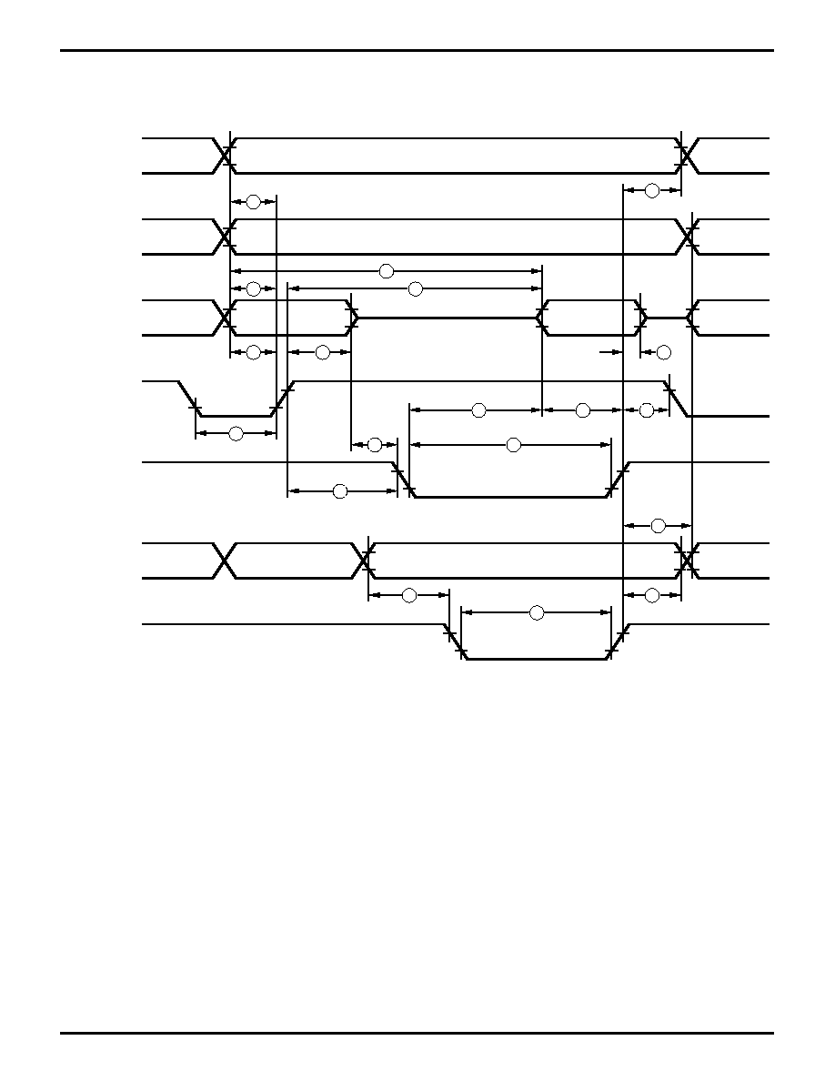
External I/O or Memory Read and Write Timing Diagram
R//W
9
12
19
3
16
13
4
5
8
18
11
6
17
10
15
7
14
2
1
Port 0, /DM
Port 1
/AS
/DS
(Read)
Port1
/DS
(Write)
A7 - A0
D7 - D0 IN
D7 - D0 OUT
A7 - A0
External I/O or Memory Read/Write Timing

14
Z89165/166/167/168/169
DTAD C
ONTROLLERS
CP96TAD0103
Z
ILOG
AC CHARACTERISTICS
Z89165/166
External I/O or Memory Read and Write Timing Table
V
CC
T
A
=0
∞
C to +70
∞
C
No
Symbol
Parameter
Note [4]
Min
Max
Units
Notes
1
TdA(AS)
Address Valid to /AS Rise Delay
5.0V
25
ns
[2,3]
2
TdAS(A)
/AS Rise to Address Float Delay
5.0V
35
ns
[2,3]
3
TdAS(DR)
/AS Rise to Read Data Req'd Valid
5.0V
150
ns
[1,2,3]
4
TwAS
/AS Low Width
5.0V
35
ns
[2,3]
5
TdAZ(DS)
Address Float to /DS Fall
5.0V
-3
ns
6
TwDSR
/DS (Read) Low Width
5.0V
125
ns
[1,2,3]
7
TwDSW
/DS (Write) Low Width
5.0V
75
ns
[1,2,3]
8
TdDSR(DR)
/DS Fall to Read Data Req'd Valid
5.0V
90
ns
[1,2,3]
9
ThDR(DS)
Read Data to /DS Rise Hold Time
5.0V
0
ns
[2,3]
10
TdDS(A)
/DS Rise to Address Active Delay
5.0V
40
ns
[2,3]
11
TdDS(AS)
/DS Rise to /AS Fall Delay
5.0V
35
ns
[2,3]
12
TdR/W(AS)
R//W Valid to /AS Rise Delay
5.0V
25
ns
[2,3]
13
TdDS(R/W)
/DS Rise to R//W Not Valid
5.0V
35
ns
[2,3]
14
TdDW(DSW) Write Data Valid to /DS Fall (Write) Delay
5.0V
40
ns
[2,3]
15
TdDS(DW)
/DS Rise to Write Data Not Valid Delay
5.0V
25
ns
[2,3]
16
TdA(DR)
Address Valid to Read Data Req'd Valid
5.0V
180
ns
[1,2,3]
17
TdAS(DS)
/AS Rise to /DS Fall Delay
5.0V
48
ns
[2,3]
18
TdDI(DS)
Data Input Setup to /DS Rise
5.0V
50
ns
[1,2,3]
19
TdDM(AS)
/DM Valid to /AS Fall Delay
5.0V
20
ns
[2,3]
Notes:
[1] When using extended memory timing add 2 TpC.
[2] Timing numbers given are for minimum TpC.
[3] See clock cycle dependent characteristics table.
[4] 5.0 V
±
0.5 V.
Standard Test Load
All timing references use 0.9 V
CC
for a logic 1 and 0.1 V
CC
for a logic 0.

15
Z89165/166/167/168/169
DTAD C
ONTROLLERS
Z
ILOG
CP96TAD0103
AC CHARACTERISTICS
Z89167/168/169
External I/O or Memory Read and Write Timing Table
V
CC
T
A
=0
∞
C to +70
∞
C
No
Symbol
Parameter
Note [4]
Min
Max
Units
Notes
1
TdA(AS)
Address Valid to /AS Rise Delay
5.0V
18
ns
[2,3]
2
TdAS(A)
/AS Rise to Address Float Delay
5.0V
22
ns
[2,3]
3
TdAS(DR)
/AS Rise to Read Data Req'd Valid
5.0V
130
ns
[1,2,3]
4
TwAS
/AS Low Width
5.0V
28
ns
[2,3]
5
TdAZ(DS)
Address Float to /DS Fall
5.0V
0
ns
6
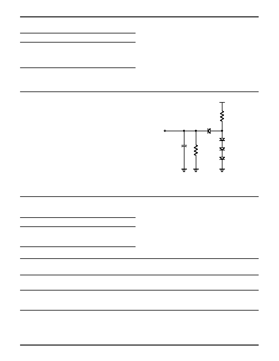
TwDSR
/DS (Read) Low Width
5.0V
90
ns
[1,2,3]
7
TwDSW
/DS (Write) Low Width
5.0V
62
ns
[1,2,3]
8
TdDSR(DR)
/DS Fall to Read Data Req'd Valid
5.0V
55
ns
[1,2,3]
9
ThDR(DS)
Read Data to /DS Rise Hold Time
5.0V
0
ns
[2,3]
10
TdDS(A)
/DS Rise to Address Active Delay
5.0V
36
ns
[2,3]
11
TdDS(AS)
/DS Rise to /AS Fall Delay
5.0V
25
ns
[2,3]
12
TdR/W(AS)
R//W Valid to /AS Rise Delay
5.0V
18
ns
[2,3]
13
TdDS(R/W)
/DS Rise to R//W Not Valid
5.0V
22
ns
[2,3]
14
TdDW(DSW) Write Data Valid to /DS Fall (Write) Delay
5.0V
18
ns
[2,3]
15
TdDS(DW)
/DS Rise to Write Data Not Valid Delay
5.0V
23
ns
[2,3]
16
TdA(DR)
Address Valid to Read Data Req'd Valid
5.0V
160
ns
[1,2,3]
17
TdAS(DS)
/AS Rise to /DS Fall Delay
5.0V
32
ns
[2,3]
18
TdDI(DS)
Data Input Setup to /DS Rise
5.0V
28
ns
[1,2,3]
19
TdDM(AS)
/DM Valid to /AS Fall Delay
5.0V
18
ns
[2,3]
Notes:
[1] When using extended memory timing add 2 TpC.
[2] Timing numbers given are for minimum TpC.
[3] See clock cycle dependent characteristics table.
[4] 5.0 V
±
0.5 V.
Standard Test Load
All timing references use 0.9 V
CC
for a logic 1 and 0.1 V
CC
for a logic 0.
16
Z89165/166/167/168/169
DTAD C
ONTROLLERS
CP96TAD0103
Z
ILOG
AC ELECTRICAL CHARACTERISTICS
Additional Timing Diagram
Clock
1
3
4
8
2
2
3
TIN
IRQN
6
5
7
7
11
Clock
Setup
10
9
Stop
Mode
Recovery
Source
Additional Timing

17
Z89165/166/167/168/169
DTAD C
ONTROLLERS
Z
ILOG
CP96TAD0103
AC ELECTRICAL CHARACTERISTICS
Z89165/166
Additional Timing Table
V
CC
T
A
=0
∞
C to +70
∞
C
No Symbol
Parameter
Note [6]
Min
Max
Units
Notes
1
TpC
Input Clock Period
5.0 V
48.83
ns
[1]
2
TrC,TfC
Clock Input Rise & Fall Times
5.0 V
6
ns
[1]
3
TwC
Input Clock Width
5.0 V
17
ns
[1]
4
TwTinL
Timer Input Low Width
5.0 V
70
ns
5
TwTinH
Timer Input High Width
5.0 V
3TpC
[1]
6
TpTin
Timer Input Period
5.0 V
8TpC
[1]
7
TrTin,
Timer Input Rise & Fall Timer
5.0 V
100
ns
[1]
TfTin
8A TwIL
Int. Request Low Time
5.0 V
70
ns
[1,2]
8B TwIL
Int. Request Low Time
5.0 V
3TpC
[1]
9
TwIH
Int. Request Input High Time
5.0 V
3TpC
[1]
10 Twsm
Stop-Mode Recovery Width Spec
5.0 V
12
ns
[1]
5TpC
11 Tost
Oscillator Startup Time
5.0 V
5TpC
[3]
12 Twdt
Watch-Dog Timer
5.0 V
3
ms
D1=0, D0 = 0 [4]
5.0 V
6
ms
D1=0, D0 = 1 [4]
5.0 V
12
ms
D1=1, D0 = 0 [4]
5.0 V
50
ms
D1=1, D0 = 1 [4]
Notes:
[1] Timing Reference uses 0.9 V
CC
for a logic 1 and 0.1 V
CC
for a logic 0.
[2] Interrupt request via Port 3 (P31-P33).
[3] SMR-D5 = 0.
[4] Reg. WDT.
[5] 5.0V
±
0.5V.

18
Z89165/166/167/168/169
DTAD C
ONTROLLERS
CP96TAD0103
Z
ILOG
AC ELECTRICAL CHARACTERISTICS
Z89167/168/169
Additional Timing Table
V
CC
T
A
=0
∞
C to +70
∞
C
No
Symbol
Parameter
Note [5]
Min
Max
Units
Notes
1
TpC
Input Clock Period
5.0 V
41.67
ns
[1]
2
TrC,TfC
Clock Input Rise & Fall Times
5.0 V
6
ns
[1]
3
TwC
Input Clock Width
5.0 V
16
ns
[1]
4
TwTinL
Timer Input Low Width
5.0 V
70
ns
5
TwTinH
Timer Input High Width
5.0 V
3TpC
[1]
6
TpTin
Timer Input Period
5.0 V
8TpC
[1]
7
TrTin,
Timer Input Rise & Fall Timer
5.0 V
100
ns
[1]
TfTin
8A
TwIL
Int. Request Low Time
5.0 V
70
ns
[1,2]
8B
TwIL
Int. Request Low Time
5.0 V
3TpC
[1]
9
TwIH
Int. Request Input High Time
5.0 V
3TpC
[1]
10
Twsm
Stop-Mode Recovery Width Spec
5.0 V
12
ns
[1]
5TpC
11
Tost
Oscillator Startup Time
5.0 V
5TpC
[3]
12
Twdt
Watch-Dog Timer
5.0 V
5
ms
D1=0, D0 = 0 [4]
5.0 V
15
ms
D1=0, D0 = 1 [4]
5.0 V
25
ms
D1=1, D0 = 0 [4]
5.0 V
100
ms
D1=1, D0 = 1 [4]
Notes:
[1] Timing Reference uses 0.9 V
CC
for a logic 1 and 0.1 V
CC
for a logic 0.
[2] Interrupt request via Port 3 (P31-P33).
[3] SMR-D5 = 0.
[4] Reg. WDT.
[5] 5.0V
±
0.5V.

19
Z89165/166/167/168/169
DTAD C
ONTROLLERS
Z
ILOG
CP96TAD0103
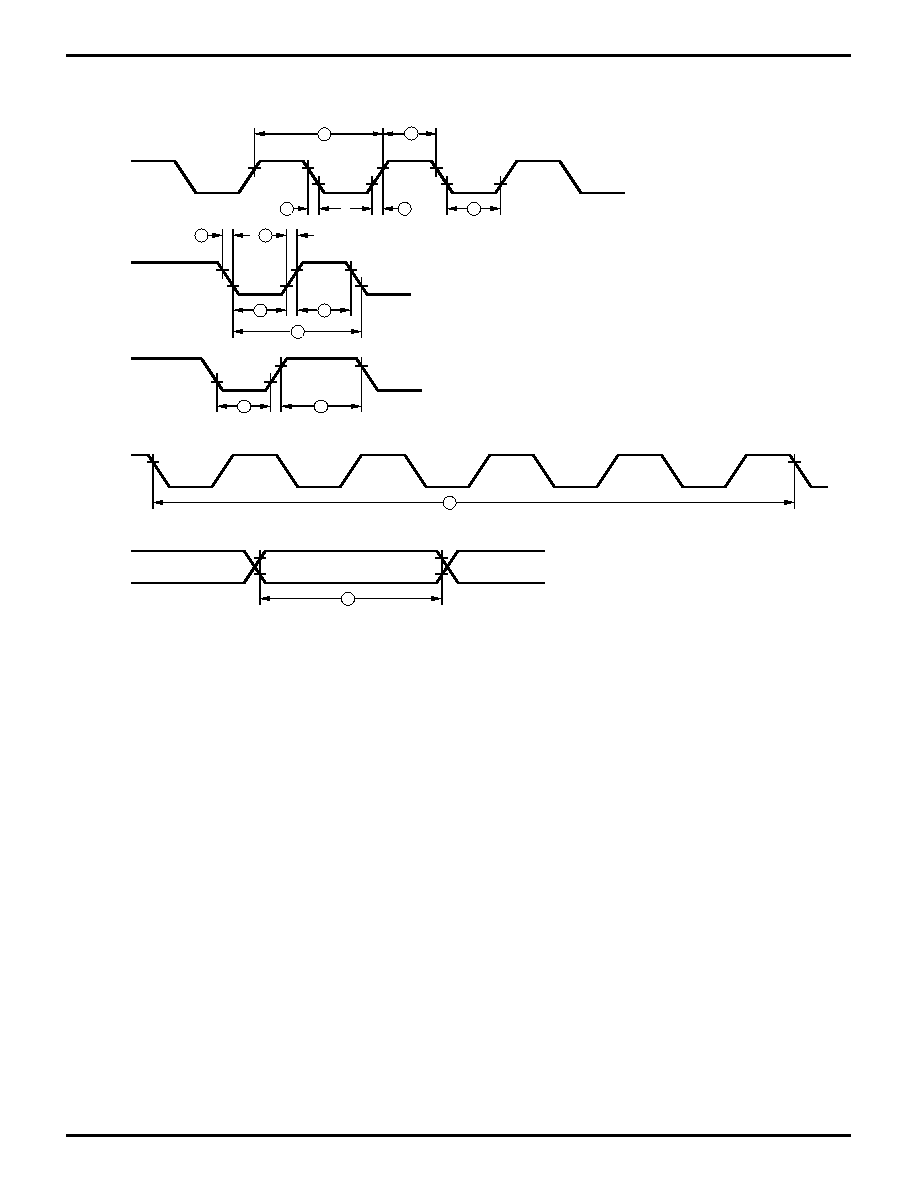
Input Handshake Timing
Data Out
/DAV
(Output)
RDY
(Input)
Next Data Out Valid
Delayed RDY
Delayed DAV
Data Out Valid
7
8
9
10
11
Output Handshake Timing
Data In
1
3
4
5
6
/DAV
(Input)
RDY
(Output)
Next Data In Valid
Delayed RDY
Delayed DAV
Data In Valid
2
AC ELECTRICAL CHARACTERISTICS
Handshake Timing Diagrams

20
Z89165/166/167/168/169
DTAD C
ONTROLLERS
CP96TAD0103
Z
ILOG
AC ELECTRICAL CHARACTERISTICS
Z89165/166
Handshake Timing Table
V
CC
T
A
=0
∞
C to +70
∞
C
Data
No
Symbol
Parameter
Note [1]
Min
Max
Units
Direction
1
TsDI(DAV)
Data In Setup Time
5.0 V
0
ns
IN
2
ThDI(RDY)
RDY to Data Hold Time
5.0 V
0
ns
IN
3
TwDAV
Data Available Width
5.0 V
40
ns
IN
4
TdDAVI(RDY)
DAV Fall to RDY Fall Delay
5.0 V
70
ns
IN
5
TdDAVId(RDY)
DAV Rise to RDY Rise Delay
5.0 V
40
ns
IN
6
TdDO(DAV)
RDY Rise to DAV Fall Delay
5.0 V
0
ns
IN
7
TcLDAV0(RDY)
Data Out to DAV Fall Delay
5.0 V
TpC
ns
OUT
8
TcLDAV0(RDY)
DAV Fall to RDY Fall Delay
5.0 V
0
ns
OUT
9
TdRDY0(DAV)
RDY Fall to DAV Rise Delay
5.0 V
70
ns
OUT
10 TwRDY
RDY Width
5.0 V
40
ns
OUT
11 TdRDY0d(DAV)
RDY Rise to DAV Fall Delay
5.0 V
40
ns
OUT
Notes:
[1] 5.0 V
±
0.5 V
AC ELECTRICAL CHARACTERISTICS
Z89167/168/169
Handshake Timing Table
V
CC
T
A
=0
∞
C to +70
∞
C
Data
No
Symbol
Parameter
Note [1]
Min
Max
Units
Direction
1
TsDI(DAV)
Data In Setup Time
5.0 V
0
ns
IN
2
ThDI(RDY)
Ready to Data In Hold Time
5.0 V
0
ns
IN
3
TwDAV
Data Available Width
5.0 V
110
ns
IN
4
TdDAVI(RDY)
DAV Fall to RDY Fall Delay
5.0 V
115
ns
IN
5
TdDAVId(RDY)
DAV Rise to RDY Rise Delay
5.0 V
80
ns
IN
6
TdDO(DAV)
RDY Rise to DAV Fall Delay
5.0 V
0
ns
IN
7
TcLDAV0(RDY)
Data Out to DAV Fall Delay
5.0 V
25
ns
OUT
8
TcLDAV0(RDY)
DAV Fall to RDY Fall Delay
5.0 V
0
ns
OUT
9
TdRDY0(DAV)
RDY Fall to DAV Rise Delay
5.0 V
115
ns
OUT
10 TwRDY
RDY Width
5.0 V
80
ns
OUT
11 TdRDY0d(DAV)
RDY Rise to DAV Fall Delay
5.0 V
80
ns
OUT
Notes:
[1] 5.0 V
±
0.5 V

21
Z89165/166/167/168/169
DTAD C
ONTROLLERS
Z
ILOG
CP96TAD0103
ELECTRICAL CHARACTERISTICS
Z89165/166 A/D CONVERTER
A/D Converter Electrical Characteristics
V
CC
= 5.0V
±
10%
Parameter
Minimum
Typical
Maximum
Units
Resolution
8
Bits
Integral non-linearity
0.5
1
LSB
Differential non-linearity
0.5
1
LSB
Zero Error at 25
∞
C
250
mV
Supply Range
4.5
5.0
5.5
Volts
Input voltage range
VA
LO
VA
HI
Volts
Conversion time
2
µ
sec
Input capacitance on ANA
25
60
pF
VA
HI
range
VA
LO
+2.5
AV
CC
Volts
VA
LO
range
AN
GND
AV
CC
≠2.5
Volts
VA
HI
-≠VA
LO
2.5
AV
CC
Volts
Notes:
Voltage 4.5V ≠5.5V
Temp 0-70
∞
C
Zilog's products are not authorized for use as critical compo-
nents in life support devices or systems unless a specific written
agreement pertaining to such intended use is executed between
the customer and Zilog prior to use. Life support devices or
systems are those which are intended for surgical implantation
into the body, or which sustains life whose failure to perform,
when properly used in accordance with instructions for use
provided in the labeling, can be reasonably expected to result in
significant injury to the user.
Zilog, Inc. 210 East Hacienda Ave.
Campbell, CA 95008-6600
Telephone (408) 370-8000
Telex 910-338-7621
FAX 408 370-8056
Internet: http://www.zilog.com
© 1997 by Zilog, Inc. All rights reserved. No part of this document
may be copied or reproduced in any form or by any means
without the prior written consent of Zilog, Inc. The information in
this document is subject to change without notice. Devices sold
by Zilog, Inc. are covered by warranty and patent indemnification
provisions appearing in Zilog, Inc. Terms and Conditions of Sale
only. Zilog, Inc. makes no warranty, express, statutory, implied or
by description, regarding the information set forth herein or
regarding the freedom of the described devices from intellectual
property infringement. Zilog, Inc. makes no warranty of mer-
chantability or fitness for any purpose. Zilog, Inc. shall not be
responsible for any errors that may appear in this document.
Zilog, Inc. makes no commitment to update or keep current the
information contained in this document.

22
Z89165/166/167/168/169
DTAD C
ONTROLLERS
CP96TAD0103
Z
ILOG