1
Z89300/01
CPS DC-4166-00
P R E L I M I N A R Y
PRELIMINARY
C
USTOMER
P
ROCUREMENT
S
PECIFICATION
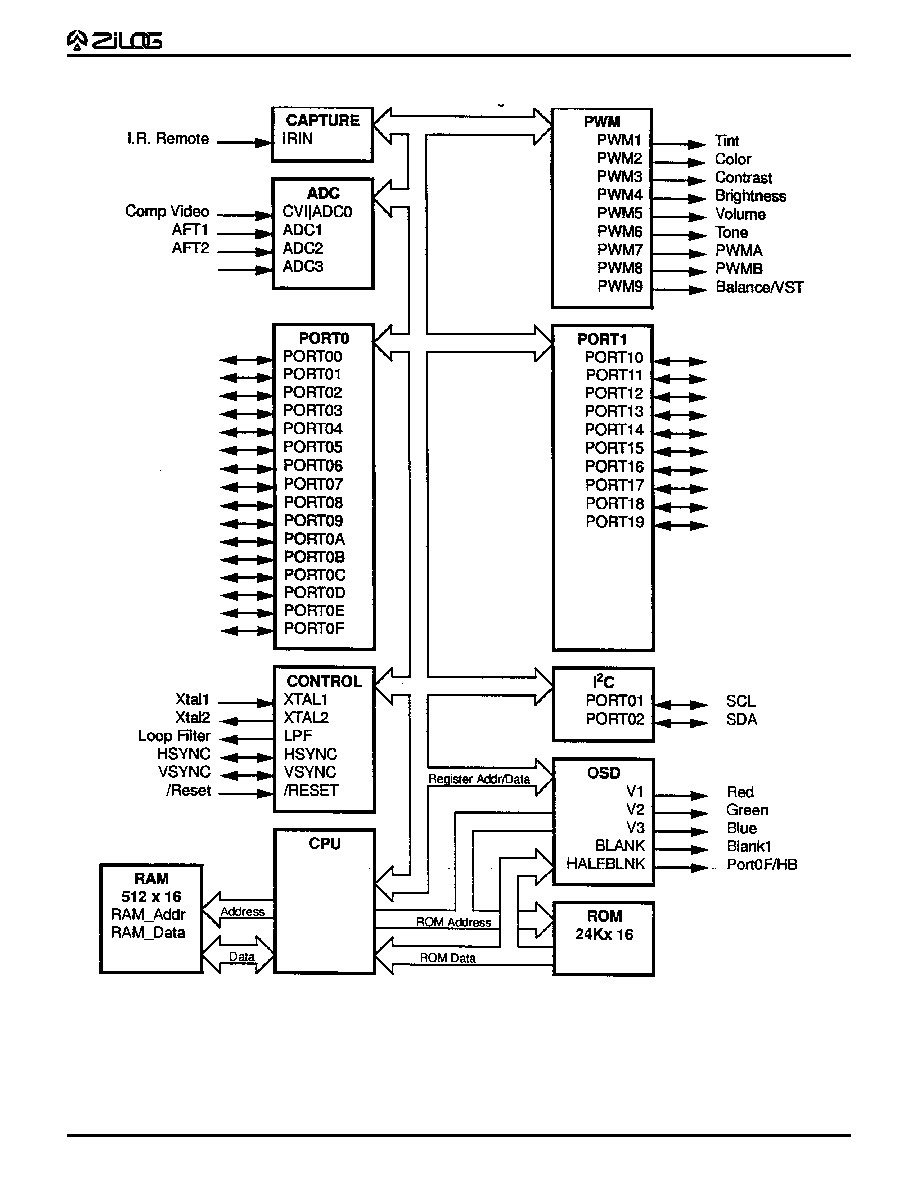
The Z89300/01 Digital Television Controller is an
application- specific controller designed to provide
complete audio and video control of television receivers,
video recorders, and advanced on-screen display facilities.
The Z89301 is the one-time-programmable (OTP) version
of the Z89300.The powerful 12 MHz Z89C00 RISC
processor core allows the user to control the on-board
peripheral functions and registers using the standard
processor instruction set.
The extensive character attributes can be controlled in two
modes: by the on-screen display controller character
control mode for maximum display control flexibility, and
closed caption mode for optimum display of closed caption
text.
Closed caption text can be decoded directly from the
composite video signal with the assistance of the
processor's digital signal processing capabilities and
displayed on the screen. The character representation in
this mode allows for a simple attribute control through the
insertion of control characters, and each word of RAM
specifies two displayed characters.
The character control mode provides access to the full set
of attribute controls. Each word of RAM specifies a single
displayed character and basic character attributes, allowing
the modification of attributes on a character-by-character
basis. The insertion of control characters permits direction
of other character attributes.
The fully customized 512 character set, formatted in two
256 character banks, can be displayed with a host of
display attributes that incude underlining, italics, blinking,
eight foreground/background colors, character position
offset delay, and background transparency. The 16-bit
display character representation allows the modification of
some key attributes on a character-by-character basis. A
character's pixel array is stored as a 16- or 18-word
representation in Character Graphics ROM (CGROM).
The ROM contents are referenced by a 16-bit word stored
in video RAM (VRAM) defining the character type and its
key attributes.
GENERAL DESCRIPTION
DC-4166-00
(8-3-93)
Z89300/01
DIGITAL TELEVISION CONTROLLER
Serial interfacing with the television tuner is provided
through the tuner serial port. Other serial devices, such as
digital channel tunning adjustments, may be accessed
through the industry standard I
2
C port.
Additional hardware provides the capability to display two
to three times normal size characters. The smoothing logic
contained in the on-screen display circuit improves the
appearance of larger fonts. Fringing circuitry can be
activated to improve the visibiity of text by surrounding the
character lines with a one-pixel border.
RGB outputs provide the direct video signals, and a
blanking output is provided to control the video multiplexor.
Dot clock and verticle line synchronization are normally
obtained from H_FLYBACK and V_FLYBACK, but can be
generated by the Z89300/01 and driven to the external
deflection unit through the bidirectional SYNC ports when
external video synchronization signals are not present.
User control can be monitored through the keypad scanning
port, or the 16-bit remote control capture register. Receiver
functions such as color and volume can be directly
controlled by eight 8-bit pulse width modulated ports.
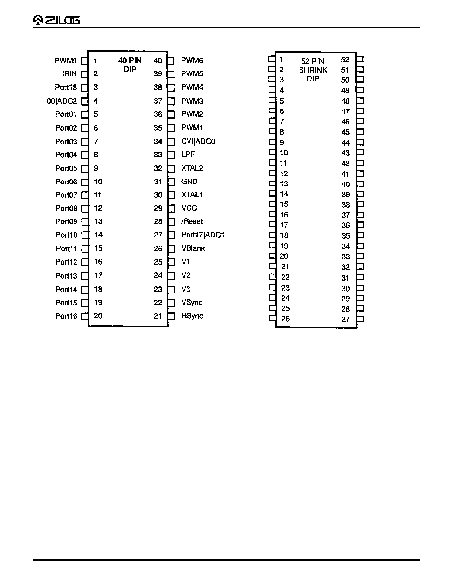
All nine PWM ports are only available in the 52-pin package.
Only six 8-bit and one 14-bit PWM output pins are available
in the 40-pin package.
The Z89300/01 has two internal 12 MHz VCOs that are
referenced to a 32 KHz internal oscillator to provide the
system clock. In Sleep mode, the controller uses the 32
KHz clock for the system clock to reduce power
consumption. The processor can be suspended by placing
it into STOP mode when main power is not available for
minimal power consumption.

5
Z89300/01
CPS DC-4166-00
P R E L I M I N A R Y
PIN DESCRIPTIONS
Z89300 (continued)
Pin
Standard
I/O/B/
Reset
Pad
Name
Application
52-Pin
40-Pin
PWR
Condition
Type
Description
PORT0 [D]
28
-
B
O
4
PORT0 [E]
5
-
B
O
4
PORT0 [F]
36
-
B
O
4
/HalfBlnk
PORT1 [0]
LED1_PWR
18
14
B
O
4
Power LED Control
PORT1 [1]
LED2_AUD
19
15
B
O
4
Mono/Stereo LED Control
PORT1 [2]
LED3_TMR
20
16
B
O
4
Timer On/OFF LED Control
PORT1 [3]
TV_VCR
21
17
B
O
4
TV/Video Switch Control
Power & Power Mgmt
PORT1 [4]
PWR_CTL
22
18
B
O
4
Power On/Off Control
PORT1 [5]
PWR_DET
23
19
B
4
Low Power Detect Input
VCC
+ 5 Volts
17
29
PWR
Supply Power
38
GND
0 Volts
10
31
PWR
Digital/Analog Ground
40
Oscillator
XTAL2
41
32
Analog
3
Oscillator Crystal Terminal 2
XTAL1
39
30
Analog
1
Oscillator Crystal Terminal 1
LPF
LOOP FILTER
42
33
I
PLL Loop Filter
RGB Display
V1
RED
33
25
O
6+Analog
Red Display Signal
V2
GREEN
32
24
O
6+Analog
Green Dislay Signal
V3
BLUE
31
23
O
6+Analog
Blue Display Signal
BLANK
BLANK
34
26
O
3
RGB Video Multipleor
Control Signal
Display Synchronization
HSYNC
H_SYNC
29
21
B
I
4
Horizontal Synchronization
Detect/Source
VSYNC
V_SYNC
30
22
B
I
4
Vertical Synchronization
Source
IRIN
REMOTE
2
2
I
1
Remote Control Capture

8
Z89300/01
CPS DC-4166-00
P R E L I M I N A R Y
Zilog's products are not authorized for use as critical compo-
nents in life support devices or systems unless a specific written
agreement pertaining to such intended use is executed between
the customer and Zilog prior to use. Life support devices or
systems are those which are intended for surgical implantation
into the body, or which sustains life whose failure to perform,
when properly used in accordance with instructions for use
provided in the labeling, can be reasonably expected to result in
significant injury to the user.
Zilog, Inc. 210 East Hacienda Ave.
Campbell, CA 95008-6600
Telephone (408) 370-8000
Telex 910-338-7621
FAX 408 370-8056
© 1993 by Zilog, Inc. All rights reserved. No part of this document
may be copied or reproduced in any form or by any means
without the prior written consent of Zilog, Inc. The information in
this document is subject to change without notice. Devices sold
by Zilog, Inc. are covered by warranty and patent indemnification
provisions appearing in Zilog, Inc. Terms and Conditions of Sale
only. Zilog, Inc. makes no warranty, express, statutory, implied or
by description, regarding the information set forth herein or
regarding the freedom of the described devices from intellectual
property infringement. Zilog, Inc. makes no warranty of mer-
chantability or fitness for any purpose. Zilog, Inc. shall not be
responsible for any errors that may appear in this document.
Zilog, Inc. makes no commitment to update or keep current the
information contained in this document.