1
Z89313
CPS5TEL0700
P R E L I M I N A R Y
CP95TEL0700 (6/95)
Z89313
DIGITAL TELEVISION CONTROLLER
FEATURES
s
Part
ROM
RAM
Speed
Number
(Word)
(Word)
(MHz)
Z89313
32K x 16
1K x 16
12
s
52-Pin Shrink DIP Package
s
4.5- to 5.5-Volt Operating Range
s
Z89C00 RISC Processor Core
s
0
∞
C to +70
∞
C Temperature Range
s
Direct Closed Caption Decoding
s
TV Tuner Serial Interface
s
Customized Character Set
s
Character Control Mode
s
Directly Controlled Receiver Functions
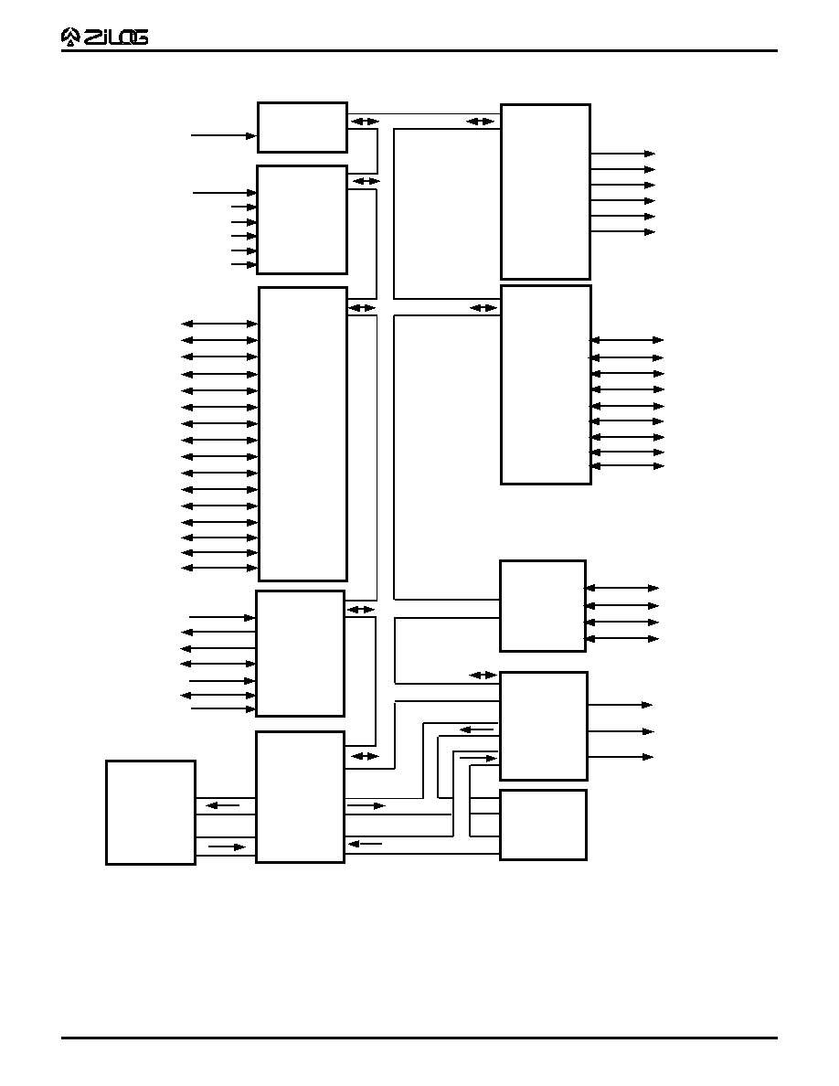
The Z89313 is a member of Zilog's family of Digital
Television Controllers designed to provide complete audio
and video control of television receivers, video recorders,
and advanced on-screen display facilities.
The Z89313 features a powerful Z89C00 RISC processor
core that controls on-board peripheral functions and
registers using the standard processor instruction set.
In closed caption mode, text can be decoded directly from
the composite video signal and displayed on the screen
with assistance from the processor's digital signal
processing capabilities. The character representation in
this mode allows for a simple attribute control through the
insertion of control characters.
The character control mode provides access to the full set
of attribute controls. The modification of attributes is allowed
on a character-by-character basis. The insertion of control
characters permits direction of other character attributes.
Display attributes, including underlining, italics, blinking,
eight foreground/background colors, character position
offset delay, and background transparency, are made
possible through a fully customized 512 character set,
formatted in two 256 character banks.
GENERAL DESCRIPTION
Serial interfacing with the television tuner is provided
through the tuner serial port. Digital channel tuning
adjustments may be accessed through the industry-
standard I
2
C port.
Additional hardware provides the capability to display two
to three times normal size characters. The smoothing logic
contained in the on-screen display circuit improves the
appearance of larger fonts. Special circuitry can be
activated to improve the visibiity of text by adding a right-
sided shadow effect to the characters.
Receiver functions such as color and volume can be
directly controlled by six 8-bit pulse width modulated
ports.
Notes:
All Signals with a preceding front slash, "/", are active Low, e.g.:
B//W (WORD is active Low); /B/W (BYTE is active Low, only).
Power connections follow conventional descriptions below:
Connection
Circuit
Device
Power
V
CC
V
DD
Ground
GND
V
SS
P
RELIMINARY
C
USTOMER
P
ROCUREMENT
S
PECIFICATION

4
Z89313
CP95TEL0700
P R E L I M I N A R Y
PIN DESCRIPTION
Z89313
Pin
Z89313
Configuration
Name
Function
52-Pin
Direction
Reset
V
CC
, ANV
CC
a
+5 V
39,22
PWR
≠
GND, ANGND,
0 V
38,21,15,40
PWR
≠
ANGNDF, ANGNDX
b
IRIN
Infrared Remote Capture Input
2
I
I
ADC[5:1]
4-Bit Analog-to-Digital Converter
16,17,18,19,20
AI
I
Input
PWM[6:1]
8-Bit Pulse Width Modulator
46,45,44,43,42,41
O
O
Output
Port0[F:0]
Bit Programmable Input/Output Ports
23,32,7,3,4,5,6,48,8,9,18,
B
I
17,10,12,11,19
Port1[8:0]
Bit Programmable Input/Output Ports
49,20,1,52,51,50,30,
B
I
31,47
SCL
I
2
C Clock I/O
11,31,34
BOD
SCD
I
2
C Data I/O
12,30,33
BOD
XTAL1
Crystal Oscillator Input
36
AI
I
XTAL2
Crystal Oscillator Output
37
AO
O
LPF
Loop Filter
14
AB
O
HSYNC
H_Sync
28,46
B
I
VSYNC
V_Sync
29
B
I
/RESET
Device Reset
35
I
I
V[3:1]
OSD Video Output
24,25,26
O
O
(Typically Drive B, G, and R Outputs)
Blank
OSD Blank Output
27
O
O
Half Blank
OSD Half Blank Output
23
O
SCLK
Internal Processor SCLK
≠
O
Notes:
Please refer to pin-out diagram for shared pin numbers.
a) AN
VCC
is for the reference voltage of the ADC input.
b) ANGND is for the reference ground of the ADC input.
ANGNDF is for LPF ground, and ANGNDX is for XTAL circuit ground.