DS000202-DSP0599
1
P
RODUCT
S
PECIFICATION
Z89223/273/323/373
16-B
IT
D
IGITAL
S
IGNAL
P
ROCESSORS
WITH
A/D C
ONVERTER
FEATURES
Operating Range
∑
5V ±10%
∑
0∞C to 70∞C Standard Temperature
≠40∞C to +85∞C Extended Temperature
DSP Core
∑
16-Bit Fixed Point DSP, 24-Bit ALU and Accumulator
∑
Single-Cycle Multiply and ALU Operations
∑
Six-Level Hardware Stack
∑
Six Data RAM Pointers and Sixteen Program Memory
Pointers
∑
RISC Processor with 30 Instruction Types
On-Chip Peripherals
∑
4-Channel, 8-Bit Half-Flash A/D Converter
∑
Serial Peripheral Interface (SPI)
∑
Three General-Purpose Counter/Timers
≠
Two Pulse Width Modulators (PWM)
≠
Two Watch-Dog Timers (WDT)
∑
Up to 40 Bits of I/O
∑
PLL System Clock
∑
Three Vectored Interrupts Servicing Eight Sources
∑
Low Power Clock Modes with Wake-up Options
GENERAL DESCRIPTION
The Z893x3 products are high-performance Digital Signal
Processors (DSP) with a modified Harvard architecture fea-
turing separate program and dual data memory banks. The
design is optimized for processing power with a minimum
of silicon area.
The Z893x3 16/24-Bit architecture accommodates ad-
vanced signal processing algorithms. The operating perfor-
mance and efficient architecture provide deterministic in-
struction execution. Compression, filtering, frequency
detection, audio, voice detection, speech synthesis, and oth-
er vital algorithms can all be implemented.
Six data RAM pointers provide circular buffer capabilities
and simultaneous dual operand fetching. Three vectored in-
terrupts are complemented by a six-level stack.
By integrating a high-speed 4-channel, 8-bit A/D, SPI, three
Counter/Timers with PWM and WDT support, and up to 40
bits of I/O, the Z893x3 family provides a compact low-cost
system solution.
To support a wide variety of development requirements, the
Z893x3 DSP product family features the cost-effective
Z89223/323 with 8 KWords of ROM. The Z89273/373, an
Device
Package
ROM
(Kwords)
OTP
(Kwords)
Data RAM
(Words)
MIPS
Z89223
44-PLCC, 44-PQFP
8
512
20
Z89273
44-PLCC
8
512
20
Z89323
64-TQFP, 68-PLCC, 80-PQFP
8
512
20
Z89373
64-TQFP, 68-PLCC, 80-PQFP
8
512
20
Z89223/273/323/373
16-Bit Digital Signal Processors with A/D Converter
ZiLOG
2
DS000202-DSP0599
GENERAL DESCRIPTION
(Continued)
OTP version of the Z89223/323, is ideal for prototypes and
early production builds.
Throughout this specification, references to the Z893x3 de-
vice apply equally to the Z89223/273/323/373, unless oth-
erwise specified.
Notes:
All signals with an overline are active Low. For
example, in RD/WR, RD is active High and WR is
active Low. For I/O ports, P1.3 denotes Port1 bit 3. Pins
called NC are "No Connection"--they do not connect
any power, grounds, or signals.
Power connections follow conventional descriptions:
Connection
Circuit
Device
Power
V
CC
V
DD
Ground
GND
V
SS
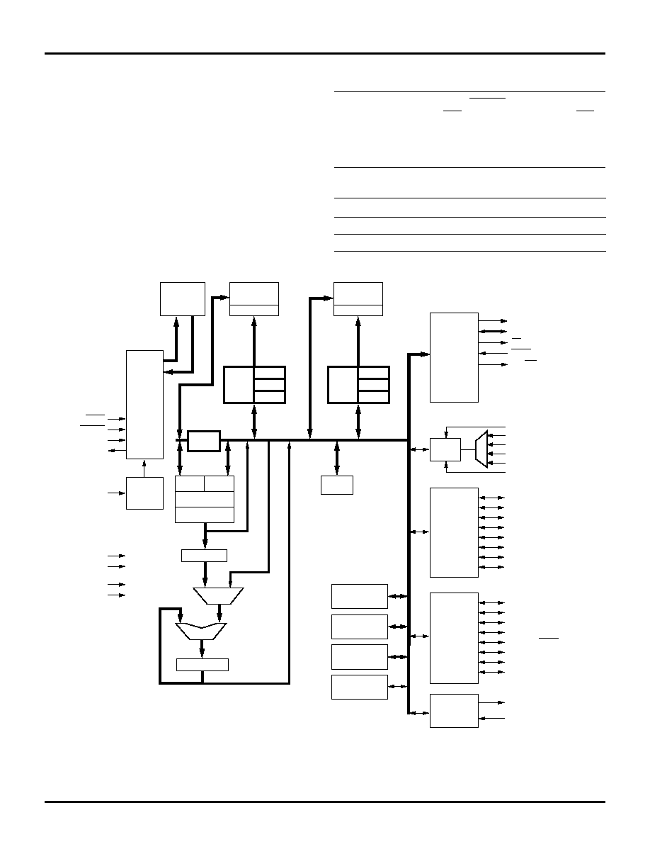
Figure 1. Z892X3/3x3 Functional Block Diagram
Data RAM1
256x16
Shifter
X
Y
Multiplier
P
P2:1
P1:1
P0:1
DADDR1
DDATA1
PDATA
DDATA0
PADDR
DDATA
8
8
8
16
16
16
16
16
16
16
16
24
16 MSB
16 MSB
24
16
16
24
24
24
16 MSB
D0:1≠3:1
Addr
Gen
Unit1
8-Bit
A/D
AN0
VAHI
EA2≠EA0
ED15≠ED0
DS
WAIT
RD/WR
Port 0
Port 1
Port 2
AN1
AN2
AN3
VALO
P1.1 or CLKOUT
P1.0 or INT2
P1.2 or SDI
P1.3 or SDO
P1.4 or SS
P1.5 or SCLK
P1.6 or UI0
P1.7 or UI1
8-Bit I/O
8-Bit I/O
16-Bit Counter
Timer
16-Bit Counter
Timer, PWM
16-Bit Counter
Timer, PWM
SPI
4 Inputs
4 Outputs
P2.1 or INT1
P2.0 or INT0
P2.2 or TMO0
P2.3 or TMO1
P2.4 or WAIT
P2.5 or UI2
P2.6 or TMO2
P2.7
P3.7≠P3.4
P3.3≠P3.0
16-Bit
Peripheral
Interface
Data RAM0
256x16
Program
ROM/OTP
8192x16
P2:0
P1:0
P0:0
DADDR0
8
D0:0≠3:0
Addr
Gen
Unit0
Program
Control
Unit
Phase
Locked
Loop
Bank
Switch
Stack
MUX
ALU
Accumulator
HALT
RESET
CLKI
CLKO
V
AGND
LPF
DD
V
SS
AV
CC
24
Z89223/273/323/373
ZiLOG
16-Bit Digital Signal Processors with A/D Converter
DS000202-DSP0599
3
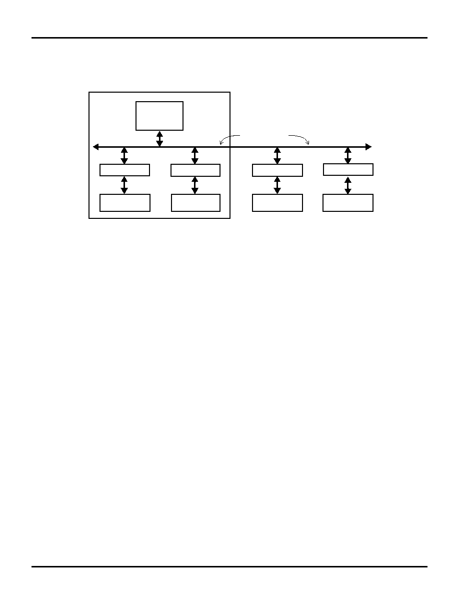
External Bus and External Registers.
The following is
made to clarify naming conventions used in this specifica-
tion. The external bus and external registers are external to
the DSP core, and are used to access internal and external
peripherals.
Figure 2. "External" Bus
DSP
Core
External Register
Internal
Peripheral
External Register
External
Peripheral
External Register
Internal
Peripheral
External Register
External
Peripheral
Z893x3
“External Bus”

Z89223/273/323/373
16-Bit Digital Signal Processors with A/D Converter
ZiLOG
4
DS000202-DSP0599
PIN FUNCTIONS
EA2≠EA0.
External Address Bus (output, latched). These
pins provide the External Register Address. This address
bus is driven during both internal and external accesses. One
of up to seven user-defined external registers is selected by
the processor for reads or writes. EXT7 is always reserved
for use by the processor.
ED15≠ED0.
External Data Bus (input/output). These pins
are the data bus for the user-defined external registers, and
are shared by Port0. These pins are normally tristated, ex-
cept when these registers are specified as destination reg-
isters in a write instruction to an external peripheral, or when
Port0 is enabled for output. This bus uses the control signals
RD/WR, DS, and WAIT, and address pins EA2≠EA0.
DS
. Data Strobe (output). This pin provides the data strobe
signal for the ED Bus. DS is active for transfers to/from ex-
ternal peripherals only.
RD/WR.
Read/Write Select (output). This pin controls the
data direction signal for the External Data Bus. Data is avail-
able from the processor on ED15≠ED0 when this signal and
DS are both Low.
WAIT
. Wait State (input). This pin is sampled at the rising
edge of the clock with appropriate setup and hold times. A
single wait-state can be generated internally by setting the
appropriate bits in the wait state register. The user must
drive this line if multiple wait states are required. This pin
is shared with Port2.
CLKI.
Clock (input). This pin is the clock circuit input. It
can be driven by a signal or connected to a 32 KHz crystal.
CLKO.
Clock (output). This pin is the clock circuit output.
It is used for operation with a 32 KHz crystal and the PLL
to generate the system clock.
HALT
. Halt State (input). This pin stops program execution.
The processor continuously executes NOPs and the pro-
gram counter remains constant while this pin is held Low.
This pin offers an internal pull-up.
RESET
. Reset (input). This pin resets the processor. It push-
es the contents of the Program Counter (PC) onto the stack
and then fetches a new PC value from program memory ad-
dress 0FFCH after the RESET signal is released. The Status
register is set to all zeros. At power-up RAM and other reg-
isters are undefined, however, they are left unchanged with
subsequent resets. RESET can be asserted asynchronously.
AN0≠AN3.
Analog Inputs (input). These are the analog in-
put pins. The analog input signal should be between VALO
and VAHI for accurate conversions.
VAHI.
Analog High Reference Voltage (input). This pin
provides the reference for the full scale voltage of the analog
input signals.
VALO.
Analog Low Reference Voltage (input). This pin
provides the reference for the zero voltage of the analog in-
put signals.
AV
CC
≠AGND.
Filtered Analog Power and Ground must be
provided on separate pins to reduce digital noise in the an-
alog circuits.
Multifunction Pins.
The Z89223/273/323/373 DSP fami-
ly offers a user-configurable I/O structure, which means
that most of the I/O pins offer dual functions. The function,
direction (input or output), and for output, the characteris-
tics (push-pull or open drain) are all under user-control, by
programming the configuration registers appropriately as
described in the I/O Ports section. The following share I/O
Port pins:
INT0≠INT2.
External Interrupts (input, edge-triggered).
These pins provide three of the eight interrupt sources to
the Interrupt Controller. Each is programmable to be rising-
edge or falling-edge triggered. The other five interrupt
sources are from the on-chip peripherals.
CLKOUT.
System Clock (output). This pin provides access
to the internal processor clock.
SDI.
Serial Data In (input). This pin is the SPI serial data
input.
SDO.
Serial Data Out (output). This pin is the SPI serial data
output.
SS.
Slave Select (input). This pin is used in SPI Slave Mode
only. SS advises the SPI that it is the target of a serial transfer
from an external Master.
SCLK.
SPI Clock (output/input). This pin is an output in
Master mode and an input in Slave mode.
UI0, UI1.
User inputs (input). These general-purpose input
pins are directly tested by the conditional branch instruc-
tions. They can also be read as bits in the status register.
These are asynchronous input signals that require no special
c l o c k s y n c h r o n i z a t i o n . C o u n t e r / T i m e r 0 a n d
Counter/Timer1 may use either of these pins as input.
UI2.
U s e r I n p u t ( i n p u t ) . T h i s p i n i s t h e i n p u t t o
Counter/Timer 2.
TMO0/UO0.
Counter/Timer Output or User Output 0 (out-
put). Counter/Timer 0 and Counter/Timer 1 can be pro-
grammed to provide output on this pin. When User Outputs
are enabled, and the Counter/Timer is disabled, this pin pro-
vides the complement of Status Register bit 5.
Z89223/273/323/373
ZiLOG
16-Bit Digital Signal Processors with A/D Converter
DS000202-DSP0599
5
TMO1/UO1.
Counter/Timer Output or User Output 1 (out-
put). Counter/Timer 0 and Counter/Timer 1 can be pro-
grammed to provide output on this pin. When User Outputs
are enabled, and the Counter/Timer is disabled, this pin pro-
vides the complement of Status Register bit 6.
TMO2.
Counter/Timer 2 Output (output). This pin is the
output of Counter/Timer 2
P0.15≠P0.0.
Port0 (input/output). This is a 16-bit user I/O
port. Bits can be configured as input or output or globally
as open-drain output. When enabled, Port0 uses the 16 data
lines of the ED bus. The function of these pins can be dy-
namically changed by writing to the Port0 configuration
registers. The High byte can also be configured to Port1 as
described in the I/O Port section.
P1.7≠P1.0.
Port1 (input/output). These pins are Port1 in-
puts or outputs when not configured for use as special pur-
pose peripheral interface. The following eight pin functions
preempt use of these pins when enabled. INT2, CLKOUT,
SDI, SDO, SS, SCLK, UI0, UI1.
Note:
These pins are not bonded out on the 44-pin packages.
P2.7≠P2.0.
Port2 (input/output). These pins are Port2 in-
puts or outputs when not configured as peripheral interfac-
es. The following seven pin functions preempt use of
P2.6≠P2.0 when enabled. INT0, INT1, TMO0/UO0,
TMO1/UO1, WAIT, UI2, TMO2. P2.7 does not include a
dual function.
Note:
P2.7≠P2.5 are not bonded out on the 44-pin packages.
The following port pins are available only on the 80-pin
package:
P3.7≠P3.4.
Port3 (output). These pins are Port3 outputs.
P3.3≠P3.0.
Port3 (input). These pins are Port3 inputs.