DS000202-DSP0599
1
P
RODUCT
S
PECIFICATION
Z89223/273/323/373
16-B
IT
D
IGITAL
S
IGNAL
P
ROCESSORS
WITH
A/D C
ONVERTER
FEATURES
Operating Range
∑
5V ±10%
∑
0∞C to 70∞C Standard Temperature
≠40∞C to +85∞C Extended Temperature
DSP Core
∑
16-Bit Fixed Point DSP, 24-Bit ALU and Accumulator
∑
Single-Cycle Multiply and ALU Operations
∑
Six-Level Hardware Stack
∑
Six Data RAM Pointers and Sixteen Program Memory
Pointers
∑
RISC Processor with 30 Instruction Types
On-Chip Peripherals
∑
4-Channel, 8-Bit Half-Flash A/D Converter
∑
Serial Peripheral Interface (SPI)
∑
Three General-Purpose Counter/Timers
≠
Two Pulse Width Modulators (PWM)
≠
Two Watch-Dog Timers (WDT)
∑
Up to 40 Bits of I/O
∑
PLL System Clock
∑
Three Vectored Interrupts Servicing Eight Sources
∑
Low Power Clock Modes with Wake-up Options
GENERAL DESCRIPTION
The Z893x3 products are high-performance Digital Signal
Processors (DSP) with a modified Harvard architecture fea-
turing separate program and dual data memory banks. The
design is optimized for processing power with a minimum
of silicon area.
The Z893x3 16/24-Bit architecture accommodates ad-
vanced signal processing algorithms. The operating perfor-
mance and efficient architecture provide deterministic in-
struction execution. Compression, filtering, frequency
detection, audio, voice detection, speech synthesis, and oth-
er vital algorithms can all be implemented.
Six data RAM pointers provide circular buffer capabilities
and simultaneous dual operand fetching. Three vectored in-
terrupts are complemented by a six-level stack.
By integrating a high-speed 4-channel, 8-bit A/D, SPI, three
Counter/Timers with PWM and WDT support, and up to 40
bits of I/O, the Z893x3 family provides a compact low-cost
system solution.
To support a wide variety of development requirements, the
Z893x3 DSP product family features the cost-effective
Z89223/323 with 8 KWords of ROM. The Z89273/373, an
Device
Package
ROM
(Kwords)
OTP
(Kwords)
Data RAM
(Words)
MIPS
Z89223
44-PLCC, 44-PQFP
8
512
20
Z89273
44-PLCC
8
512
20
Z89323
64-TQFP, 68-PLCC, 80-PQFP
8
512
20
Z89373
64-TQFP, 68-PLCC, 80-PQFP
8
512
20
Z89223/273/323/373
16-Bit Digital Signal Processors with A/D Converter
ZiLOG
2
DS000202-DSP0599
GENERAL DESCRIPTION
(Continued)
OTP version of the Z89223/323, is ideal for prototypes and
early production builds.
Throughout this specification, references to the Z893x3 de-
vice apply equally to the Z89223/273/323/373, unless oth-
erwise specified.
Notes:
All signals with an overline are active Low. For
example, in RD/WR, RD is active High and WR is
active Low. For I/O ports, P1.3 denotes Port1 bit 3. Pins
called NC are "No Connection"--they do not connect
any power, grounds, or signals.
Power connections follow conventional descriptions:
Connection
Circuit
Device
Power
V
CC
V
DD
Ground
GND
V
SS
Figure 1. Z892X3/3x3 Functional Block Diagram
Data RAM1
256x16
Shifter
X
Y
Multiplier
P
P2:1
P1:1
P0:1
DADDR1
DDATA1
PDATA
DDATA0
PADDR
DDATA
8
8
8
16
16
16
16
16
16
16
16
24
16 MSB
16 MSB
24
16
16
24
24
24
16 MSB
D0:1≠3:1
Addr
Gen
Unit1
8-Bit
A/D
AN0
VAHI
EA2≠EA0
ED15≠ED0
DS
WAIT
RD/WR
Port 0
Port 1
Port 2
AN1
AN2
AN3
VALO
P1.1 or CLKOUT
P1.0 or INT2
P1.2 or SDI
P1.3 or SDO
P1.4 or SS
P1.5 or SCLK
P1.6 or UI0
P1.7 or UI1
8-Bit I/O
8-Bit I/O
16-Bit Counter
Timer
16-Bit Counter
Timer, PWM
16-Bit Counter
Timer, PWM
SPI
4 Inputs
4 Outputs
P2.1 or INT1
P2.0 or INT0
P2.2 or TMO0
P2.3 or TMO1
P2.4 or WAIT
P2.5 or UI2
P2.6 or TMO2
P2.7
P3.7≠P3.4
P3.3≠P3.0
16-Bit
Peripheral
Interface
Data RAM0
256x16
Program
ROM/OTP
8192x16
P2:0
P1:0
P0:0
DADDR0
8
D0:0≠3:0
Addr
Gen
Unit0
Program
Control
Unit
Phase
Locked
Loop
Bank
Switch
Stack
MUX
ALU
Accumulator
HALT
RESET
CLKI
CLKO
V
AGND
LPF
DD
V
SS
AV
CC
24
Z89223/273/323/373
ZiLOG
16-Bit Digital Signal Processors with A/D Converter
DS000202-DSP0599
3
External Bus and External Registers.
The following is
made to clarify naming conventions used in this specifica-
tion. The external bus and external registers are external to
the DSP core, and are used to access internal and external
peripherals.
Figure 2. "External" Bus
DSP
Core
External Register
Internal
Peripheral
External Register
External
Peripheral
External Register
Internal
Peripheral
External Register
External
Peripheral
Z893x3
“External Bus”

Z89223/273/323/373
16-Bit Digital Signal Processors with A/D Converter
ZiLOG
4
DS000202-DSP0599
PIN FUNCTIONS
EA2≠EA0.
External Address Bus (output, latched). These
pins provide the External Register Address. This address
bus is driven during both internal and external accesses. One
of up to seven user-defined external registers is selected by
the processor for reads or writes. EXT7 is always reserved
for use by the processor.
ED15≠ED0.
External Data Bus (input/output). These pins
are the data bus for the user-defined external registers, and
are shared by Port0. These pins are normally tristated, ex-
cept when these registers are specified as destination reg-
isters in a write instruction to an external peripheral, or when
Port0 is enabled for output. This bus uses the control signals
RD/WR, DS, and WAIT, and address pins EA2≠EA0.
DS
. Data Strobe (output). This pin provides the data strobe
signal for the ED Bus. DS is active for transfers to/from ex-
ternal peripherals only.
RD/WR.
Read/Write Select (output). This pin controls the
data direction signal for the External Data Bus. Data is avail-
able from the processor on ED15≠ED0 when this signal and
DS are both Low.
WAIT
. Wait State (input). This pin is sampled at the rising
edge of the clock with appropriate setup and hold times. A
single wait-state can be generated internally by setting the
appropriate bits in the wait state register. The user must
drive this line if multiple wait states are required. This pin
is shared with Port2.
CLKI.
Clock (input). This pin is the clock circuit input. It
can be driven by a signal or connected to a 32 KHz crystal.
CLKO.
Clock (output). This pin is the clock circuit output.
It is used for operation with a 32 KHz crystal and the PLL
to generate the system clock.
HALT
. Halt State (input). This pin stops program execution.
The processor continuously executes NOPs and the pro-
gram counter remains constant while this pin is held Low.
This pin offers an internal pull-up.
RESET
. Reset (input). This pin resets the processor. It push-
es the contents of the Program Counter (PC) onto the stack
and then fetches a new PC value from program memory ad-
dress 0FFCH after the RESET signal is released. The Status
register is set to all zeros. At power-up RAM and other reg-
isters are undefined, however, they are left unchanged with
subsequent resets. RESET can be asserted asynchronously.
AN0≠AN3.
Analog Inputs (input). These are the analog in-
put pins. The analog input signal should be between VALO
and VAHI for accurate conversions.
VAHI.
Analog High Reference Voltage (input). This pin
provides the reference for the full scale voltage of the analog
input signals.
VALO.
Analog Low Reference Voltage (input). This pin
provides the reference for the zero voltage of the analog in-
put signals.
AV
CC
≠AGND.
Filtered Analog Power and Ground must be
provided on separate pins to reduce digital noise in the an-
alog circuits.
Multifunction Pins.
The Z89223/273/323/373 DSP fami-
ly offers a user-configurable I/O structure, which means
that most of the I/O pins offer dual functions. The function,
direction (input or output), and for output, the characteris-
tics (push-pull or open drain) are all under user-control, by
programming the configuration registers appropriately as
described in the I/O Ports section. The following share I/O
Port pins:
INT0≠INT2.
External Interrupts (input, edge-triggered).
These pins provide three of the eight interrupt sources to
the Interrupt Controller. Each is programmable to be rising-
edge or falling-edge triggered. The other five interrupt
sources are from the on-chip peripherals.
CLKOUT.
System Clock (output). This pin provides access
to the internal processor clock.
SDI.
Serial Data In (input). This pin is the SPI serial data
input.
SDO.
Serial Data Out (output). This pin is the SPI serial data
output.
SS.
Slave Select (input). This pin is used in SPI Slave Mode
only. SS advises the SPI that it is the target of a serial transfer
from an external Master.
SCLK.
SPI Clock (output/input). This pin is an output in
Master mode and an input in Slave mode.
UI0, UI1.
User inputs (input). These general-purpose input
pins are directly tested by the conditional branch instruc-
tions. They can also be read as bits in the status register.
These are asynchronous input signals that require no special
c l o c k s y n c h r o n i z a t i o n . C o u n t e r / T i m e r 0 a n d
Counter/Timer1 may use either of these pins as input.
UI2.
U s e r I n p u t ( i n p u t ) . T h i s p i n i s t h e i n p u t t o
Counter/Timer 2.
TMO0/UO0.
Counter/Timer Output or User Output 0 (out-
put). Counter/Timer 0 and Counter/Timer 1 can be pro-
grammed to provide output on this pin. When User Outputs
are enabled, and the Counter/Timer is disabled, this pin pro-
vides the complement of Status Register bit 5.

Z89223/273/323/373
ZiLOG
16-Bit Digital Signal Processors with A/D Converter
DS000202-DSP0599
5
TMO1/UO1.
Counter/Timer Output or User Output 1 (out-
put). Counter/Timer 0 and Counter/Timer 1 can be pro-
grammed to provide output on this pin. When User Outputs
are enabled, and the Counter/Timer is disabled, this pin pro-
vides the complement of Status Register bit 6.
TMO2.
Counter/Timer 2 Output (output). This pin is the
output of Counter/Timer 2
P0.15≠P0.0.
Port0 (input/output). This is a 16-bit user I/O
port. Bits can be configured as input or output or globally
as open-drain output. When enabled, Port0 uses the 16 data
lines of the ED bus. The function of these pins can be dy-
namically changed by writing to the Port0 configuration
registers. The High byte can also be configured to Port1 as
described in the I/O Port section.
P1.7≠P1.0.
Port1 (input/output). These pins are Port1 in-
puts or outputs when not configured for use as special pur-
pose peripheral interface. The following eight pin functions
preempt use of these pins when enabled. INT2, CLKOUT,
SDI, SDO, SS, SCLK, UI0, UI1.
Note:
These pins are not bonded out on the 44-pin packages.
P2.7≠P2.0.
Port2 (input/output). These pins are Port2 in-
puts or outputs when not configured as peripheral interfac-
es. The following seven pin functions preempt use of
P2.6≠P2.0 when enabled. INT0, INT1, TMO0/UO0,
TMO1/UO1, WAIT, UI2, TMO2. P2.7 does not include a
dual function.
Note:
P2.7≠P2.5 are not bonded out on the 44-pin packages.
The following port pins are available only on the 80-pin
package:
P3.7≠P3.4.
Port3 (output). These pins are Port3 outputs.
P3.3≠P3.0.
Port3 (input). These pins are Port3 inputs.
Z89223/273/323/373
16-Bit Digital Signal Processors with A/D Converter
ZiLOG
6
DS000202-DSP0599
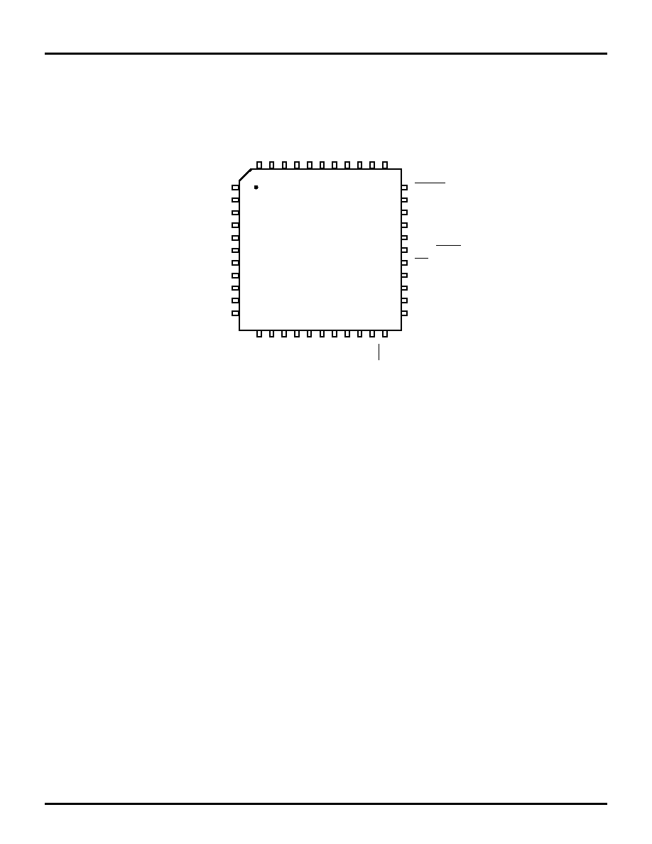
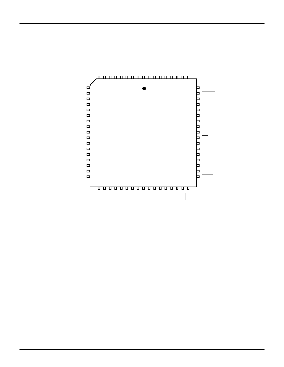
PIN CONFIGURATIONS
Figure 3. 44-Pin PLCC Z89223/273 Pin Configuration
44-Pin
PLCC
7
8
9
10
11
12
13
14
15
16
17
ED3/P0.3
ED4/P0.4
V
SS
ED5/P0.5
ED6/P0.6
ED7/P0.7
ED8/P0.8
ED9/P0.9
V
SS
ED10/P0.10
ED11/P0.11
RESET
LPF
P2.2/TMO0/UO0
CLKO
CLKI
P2.4/WAIT
DS
P2.3/TMO1/UO1
EA2
EA1
EA0
V
AHI
V
ALO
AGND
AN0
AN1
AN2
AN3
P2.1/INT1
AV
CC
V
DD
RD/WR
ED15/P0.15
V
SS
ED14/P0.14
ED13/P0.13
ED12/P0.12
P2.0/INT0
V
SS
ED2/P0.2
ED1/P0.1
ED0/P0.0
V
DD
1
28
18
40
6
39
38
37
36
35
34
33
32
31
30
29
20
22
24
26
4
42
Z89223/273/323/373
ZiLOG
16-Bit Digital Signal Processors with A/D Converter
DS000202-DSP0599
7
Table 1. 44-Pin PLCC Z89223/273 Pin Description
No Symbol
Function
Direction
No Symbol
Function
Direction
1
P2.0/INT0
Port 2.0/Interrupt 0
Input/Output
23
AN2
A/D Input 2
Input
2
ED12/P0.12
External Data Bus/Port0
Input/Output
24
AN3
A/D Input 3
Input
3
ED13/P0.13
External Data Bus/Port0
Input/Output
25
P2.1/INT1
Port 2.1/Interrupt 1
Input/Output
4
ED14/P0.14
External Data Bus/Port0
Input/Output
26
AV
CC
Analog Power
5
V
SS
Ground
27
V
DD
Power Supply
6
ED15/P0.15
External Data Bus/Port0
Input/Output
28
RD/WR
R/W External Bus
Output
7
ED3/P0.3
External Data Bus/Port0
Input/Output
29
EA0
Ext Address 0
Output
8
ED4/P0.4
External Data Bus/Port0
Input/Output
30
EA1
Ext Address 1
Output
9
V
SS
Ground
31
EA2
Ext Address 2
Output
10
ED5/P0.5
External Data Bus/Port0
Input/Output
32
P2.3/TMO1
Port 2.3/Timer Output 1
Input/Output
11
ED6/P0.6
External Data Bus/Port0
Input/Output
33
DS
Ext Data Strobe
Output
12
ED7/P0.7
External Data Bus/Port0
Input/Output
34
P2.4/WAIT
Port 2.4/Wait for ED
Input/Output
13
ED8/P0.8
External Data Bus/Port0
Input/Output
35
CLKI
Clock/Crystal In
Input
14
ED9/P0.9
External Data Bus/Port0
Input/Output
36
CLKO
Clock/Crystal Out
Output
15
V
SS
Ground
37
P2.2/TMO0
Port 2.2/Timer Output 0
Input/Output
16
ED10/P0.10
External Data Bus/Port0
Input/Output
38
LPF
PLL Low Pass Filter
Input
17
ED11/P0.11
External Data Bus/Port0
Input/Output
39
RESET
Reset
Input
18
VAHI
Analog High Ref. Voltage
Input
40
V
DD
Power
19
VALO
Analog Low Ref. Voltage
Input
41
ED0/P0.0
External Data Bus/Port0
Input/Output
20
AGND
Analog Ground
42
ED1/P0.1
External Data Bus/Port0
Input/Output
21
AN0
A/D Input 0
Input
43
ED2/P0.2
External Data Bus/Port0
Input/Output
22
AN1
A/D Input 1
Input
44
V
S
S
Ground
Z89223/273/323/373
16-Bit Digital Signal Processors with A/D Converter
ZiLOG
8
DS000202-DSP0599
PIN CONFIGURATIONS (Continued)
Figure 4. 44-Pin PQFP Z89223/273 Pin Configuration
ED15/P0.15
V
SS
ED14/P/P0.14
ED13/P0.13
ED12/P0.12
P2.0/INT0
V
SS
ED2/P0.2
ED1/P0.1
ED0/P0.0
V
DD
V
AHI
V
ALO
AGND
AN0
AN1
AN2
AN3
P2.1/INT1
AV
CC
V
DD
RD/WR
ED3/P0.3
ED4/P0.4
V
SS
ED5/P0.5
ED6/P0.6
ED7/P0.7
ED8/P0.8
ED9/P0.9
V
SS
ED10/P0.10
ED11/P0.11
RESET
LPF
P2.2/TMO0/UO0
CLKO
CLKI
P2.4/WAIT
DS
P2.3/TMO1/UO1
EA2
EA1
EA0
1
23
33
44-Pin
PQFP
11
25
27
29
31
9
7
5
3
44 43 42 41 40 39 38 37 36 35 34
12 13 14 15 16 17 18 19 20 21 22
Z89223/273/323/373
ZiLOG
16-Bit Digital Signal Processors with A/D Converter
DS000202-DSP0599
9
Table 2. 44-Pin PQFP Z89223/273 Pin Description
No
Symbol
Function
Direction
No
Symbol
Function
Direction
1
ED3/P0.3
External Data Bus/Port0
Input/Output
23
EA0
Ext Address 0
Output
2
ED4/P0.4
External Data Bus/Port0
Input/Output
24
EA1
Ext Address 1
Output
3
V
SS
Ground
25
EA2
Ext Address 2
Output
4
ED5/P0.5
External Data Bus/Port0
Input/Output
26
P2.3/TMO1
Port 2.3/Timer Output 1
Input/Output
5
ED6/P0.6
External Data Bus/Port0
Input/Output
27
DS
Ext Data Strobe
Output
6
ED7/P0.7
External Data Bus/Port0
Input/Output
28
P2.4/WAIT
Port 2.4/Wait for ED
Input/Output
7
ED8/P0.8
External Data Bus/Port0
Input/Output
29
CLKI
Clock/Crystal In
Input
8
ED9/P0.9
External Data Bus/Port0
Input/Output
30
CLKO
Clock/Crystal Out
Output
9
V
SS
Ground
31
P2.2/TMO0
Port 2.2/Timer Output 0
Input/Output
10
ED10/P0.10
External Data Bus/Port0
Input/Output
32
LPF
PLL Low Pass Filter
Input
11
ED11/P0.11
External Data Bus/Port0
Input/Output
33
RESET
Reset
Input
12
VAHI
Analog High Ref. Voltage
Input
34
V
DD
Power Supply
13
VALO
Analog Low Ref. Voltage
Input
35
ED0/P0.0
External Data Bus/Port0
Input/Output
14
AGND
Analog Ground
36
ED1/P0.1
External Data Bus/Port0
Input/Output
15
AN0
A/D Input 0
Input
37
ED2/P0.2
External Data Bus/Port0
Input/Output
16
AN1
A/D Input 1
Input
38
V
SS
Ground
17
AN2
A/D Input 2
Input
39
P2.0/INT0
Port 2.0/Interrupt 0
Input/Output
18
AN3
A/D Input 3
Input
40
ED12/P0.12
External Data Bus/Port0
Input/Output
19
P2.1/INT1
Port 2.1/Interrupt 1
Input/Output
41
ED13/P0.13
External Data Bus/Port0
Input/Output
20
AV
CC
Analog Power
42
ED14/P0.14
External Data Bus/Port0
Input/Output
21
V
DD
Power
43
V
SS
Ground
22
RD/WR
R/W Exteral Output Bus
44
ED15/P0.15
External Data Bus/Port0
Input/Output
Z89223/273/323/373
16-Bit Digital Signal Processors with A/D Converter
ZiLOG
10
DS000202-DSP0599
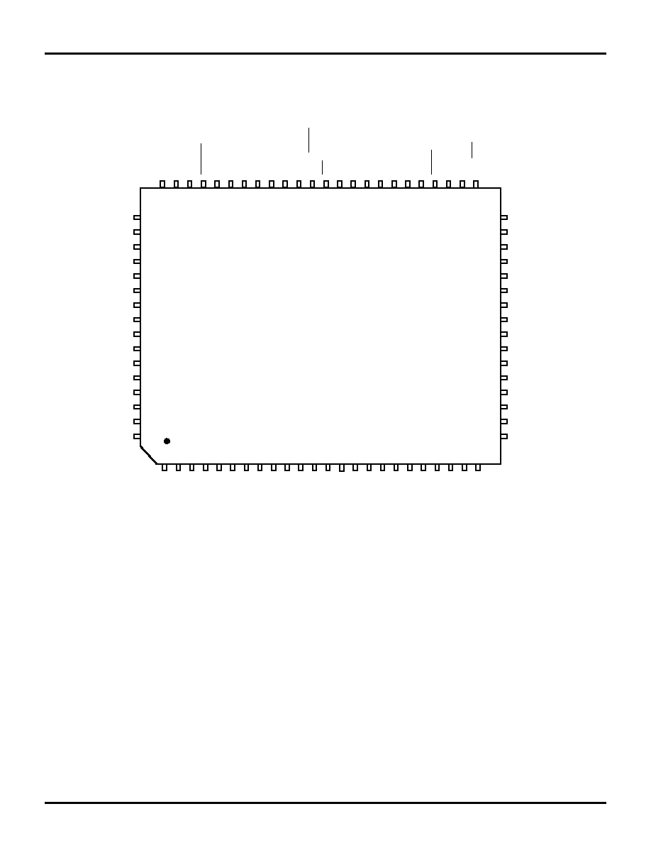
PIN CONFIGURATIONS (Continued)
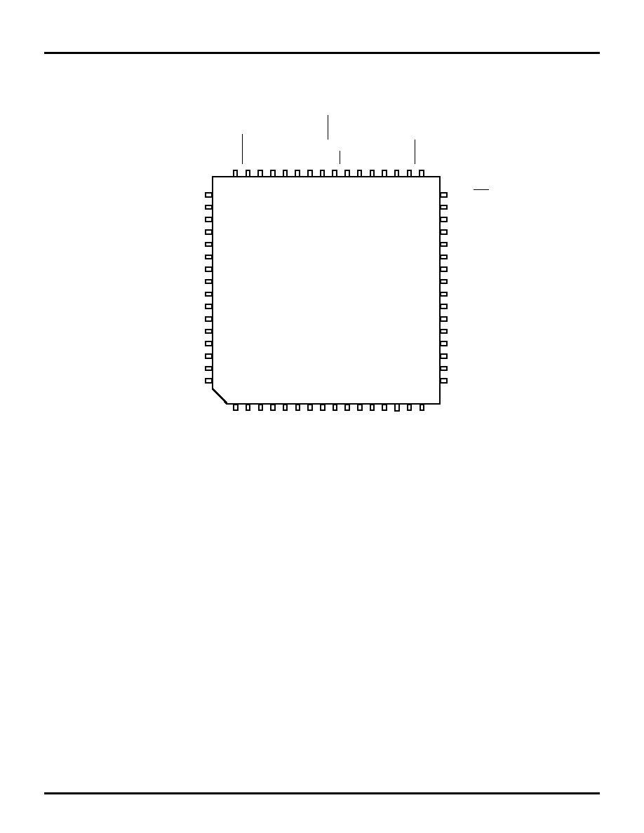
Figure 5. 64-Pin TQFP Z89323/373 Pin Configuration
32
30
25
20
17
49
55
60
64
V
DD
V
SS
ED0/P0.0
ED1/P0.1
ED2/P0.2
P1.0/INT2
V
SS
P1.1/CLKOUT
P1.2/SDI
P2.0/INT0
ED12/P0.12
ED13/P0.13
V
DD
ED14/P0.14
V
SS
ED15/P0.15
RD/WR
V
DD
AV
CC
P2.1/INT1
V
SS
AN3
AN2
AN1
AN0
AGND
P1.7/UI1
VALO
P1.6/UI0
V
SS
VAHI
ED11/P0.11
ED3/P0.3
ED4/P0.4
V
SS
V
DD
ED5/P0.5
P1.3/SDO
ED6/P0.6
P1.4/SS
ED7/P0.7
P1.5/SCLK
P2.7
ED8/P0.8
ED9/P0.9
V
SS
ED10/P0.10
V
SS
V
SS
RESET
LPF
P2.5/UI2
P2.2/TMO0/UO0
P2.6/TMO2
CLKO
CLKI
P2.4/ W
AIT
DS
P2.3/TMO1/UO1
V
DD
EA2
EA1
EA0
HAL
T
1
33
48
64-Pin
TQFP
16
5
10
35
40
45

Z89223/273/323/373
ZiLOG
16-Bit Digital Signal Processors with A/D Converter
DS000202-DSP0599
11
Table 3. 64-Pin TQFP Z89223/273 Pin Description
No Symbol
Function
Direction
No Symbol
Function
Direction
1
ED3/P0.3
External Data Bus/Port0
Input/Output
33 HALT
Halt Execution
Input
2
ED4/P0.4
External Data Bus/Port0
Input/Output
34 EA0
Ext Address 0
Output
3
V
SS
Ground
35 EA1
Ext Address 1
Output
4
V
DD
Power Supply
36 EA2
Ext Address 2
Output
5
ED5/P0.5
External Data Bus/Port0
Input/Output
37 V
DD
Power Supply
6
P1.3/SDO
Port 1.3/Serial Output
Input/Output
38 P2.3/TMO1
Port2.3/Timer Output 1
Input/Output
7
ED6/P0.6
External Data Bus/Port0
Input/Output
39 DS
Ext Data Strobe
Output
8
P1.4/SS
Port 1.4/Slave Select
Input/Output
40 P2.4/WAIT
Port 2.4/Wait for ED
Input/Output
9
ED7/P0.7
External Data Bus/Port0
Input/Output
41 CLKI
Clock/Crystal In
Input
10 P1.5/SCLK
Port 1.5/Serial Clock
Input/Output
42 CLKO
Clock/Crystal Out
Output
11 P2.7
Port 2.7
Input/Output
43 P2.6/TMO2
Port 2.6/Timer Output 2
Input/Output
12 ED8/P0.8
External Data Bus/Port0
Input/Output
44 P2.2/TMO0
Port 2.2/Timer Output 0
Input/Output
13 ED9/P0.9
External Data Bus/Port0
Input/Output
45 P2.5/UI2
Port 2.5/User Input 2
Input/Output
14 V
SS
Ground
46 LPF
PLL Low Pass Filter
Input
15 ED10/P0.10
External Data Bus/Port0
Input/Output
47 RESET
Reset
Input
16 V
SS
Ground
48 V
SS
Ground
17 ED11/P0.11
External Data Bus/Port0
Input/Output
49 V
DD
Power Supply
18 VAHI
Analog High Ref. Voltage
Input
50 V
SS
Ground
19 V
SS
Ground
51 ED0/P0.0
External Data Bus/Port0
Input/Output
20 P1.6/UI0
Port 1.6/User Input 0
Input/Output
52 ED1/P0.1
External Data Bus/Port0
Input/Output
21 VALO
Analog Low Ref. Voltage
Input
53 ED2/P0.2
External Data Bus/Port0
Input/Output
22 P1.7/UI1
Port 1.7/User Input 1
Input/Output
54 P1.0/INT2
Port 1.0/Interrupt 2
Input/Output
23 AGND
Analog Ground
55 V
SS
Ground
24 AN0
A/D Input 0
Input
56 P1.1/CLKOUT Port 1.1/Clock Output
Input/Output
25 AN1
A/D Input 1
Input
57 P1.2/SDI
Port 1.2/Serial Input
Input/Output
26 AN2
A/D Input 2
Input
58 P2.0/INT0
Port 2.0/Interrupt 0
Input/Output
27 AN3
A/D Input 3
Input
59 ED12/P0.12
External Data Bus/Port0
Input/Output
28 V
SS
Ground
60 ED13/P0.13
External Data Bus/Port0
Input/Output
29 P2.1/INT1
Port 2.1/Interrupt 1
Input/Output
61 V
DD
Power Supply
30 AVCC
Analog Power
62 ED14/P0.14
External Data Bus/Port0
Input/Output
31 V
DD
Power Supply
63 V
SS
Ground
32 RD/WR
R/W External Bus
Output
64 ED15/P0.15
External Data Bus/Port0
Input/Output
Z89223/273/323/373
16-Bit Digital Signal Processors with A/D Converter
ZiLOG
12
DS000202-DSP0599
PIN CONFIGURATIONS (Continued)
Figure 6. 68-Pin PLCC Z89323/373 Pin Configuration
60
44
10
26
NC
ED3/P0.3
ED4/P0.4
V
SS
V
DD
ED5/P0.5
P1.3/SDO
ED6/P0.6
P1.4/SS
ED7/P0.7
P1.5/SCLK
P2.7
ED8/P0.8
ED9/P0.9
V
SS
ED10/P0.10
V
SS
NC
ED15/P0.15
V
SS
ED14/P0.14
V
DD
ED13/P0.13
ED12/P0.12
P2.0/INT0
P1.2/SDI
P1.1/CLKOUT
V
SS
P1.0/INT2
ED2/P0.2
ED1/P0.1
ED0/P0.0
V
SS
V
DD
43
27
61
9
68-Pin
PLCC
1
V
SS
RESET
LPF
P2.5/UI2
P2.2/TMO0/UO0
P2.6/TMO2
CLKO
CLKI
P2.4/WAIT
DS
P2.3/TMO1/UO1
V
DD
NC
EA2
EA1
EA0
HALT
ED11/P0.11
V
DD
V
AHI
V
SS
P1.6/UI0
V
ALO
P1.7/UI1
AGND
AN0
AN1
AN2
AN3
V
SS
P2.1/INT1
AV
CC
V
DD
RD/WR
Z89223/273/323/373
ZiLOG
16-Bit Digital Signal Processors with A/D Converter
DS000202-DSP0599
13
Table 4. 68-Pin PLCC Z89323/373 Pin Description
No Symbol
Function
Direction
No Symbol
Function
Direction
1
P1.2/SDI
Port 1.2/Serial Input
Input/Output
35 AN0
A/D Input 0
Input
2
P2.0/INT0
Port 2.0/Interrupt 0
Input/Output
36 AN1
A/D Input 1
Input
3
ED12/P0.12
External Data Bus/Port0
Input/Output
37 AN2
A/D Input 2
Input
4
ED13/P0.13
External Data Bus/Port0
Input/Output
38 AN3
A/D Input 3
Input
5
V
DD
Power Supply
39 V
SS
Ground
6
ED14/P0.14
External Data Bus/Port0
Input/Output
40 P2.1/INT1
Port 2.1/Interrupt 1
Input/Output
7
V
SS
Ground
41 AVCC
Analog Power
8
ED15/P0.15
External Data Bus/Port0
Input/Output
42 V
DD
Power Supply
9
NC
No Connection
43 RD/WR
R/W External Bus
Output
10 NC
No Connection
44 HALT
Halt Execution
Input
11 ED3/P0.3
External Data Bus/Port0
Input/Output
45 EA0
Ext Address 0
Output
12 ED4/P0.4
External Data Bus/Port0
Input/Output
46 EA1
Ext Address 1
Output
13 V
SS
Ground
47 EA2
Ext Address 2
Output
14 V
DD
Power Supply
48 NC
No Connection
15 ED5/P0.5
External Data Bus/Port0
Input/Output
49 V
DD
Power Supply
16 P1.3/SDO
Port 1.3/Serial Output
Input/Output
50 P2.3/TMO1
Port2.3/Timer Output 1
Input/Output
17 ED6/P0.6
External Data Bus/Port0
Input/Output
51 DS
Ext Data Strobe
Output
18 P1.4/SS
Port 1.4/Slave Select
Input/Output
52 P2.4/WAIT
Port 2.4/Wait for ED
Input/Output
19 ED7/P0.7
External Data Bus/Port0
Input/Output
53 CLKI
Clock/Crystal In
Input
20 P1.5/SCLK
Port 1.5/Serial Clock
Input/Output
54 CLKO
Clock/Crystal Out
Output
21 P2.7
Port 2.7
Input/Output
55 P2.6/TMO2
Port 2.6/Timer Output 2
Input/Output
22 ED8/P0.8
External Data Bus/Port0
Input/Output
56 P2.2/TMO0
Port 2.2/Timer Output 0
Input/Output
23 ED9/P0.9
External Data Bus/Port0
Input/Output
57 P2.5/UI2
Port 2.5/User Input 2
Input/Output
24 V
SS
Ground
58 LPF
PLL Low Pass Filter
Input
25 ED10/P0.10
External Data Bus/Port0
Input/Output
59 RESET
Reset
Input
26 V
SS
Ground
60 V
SS
Ground
27 ED11/P0.11
External Data Bus/Port0
Input/Output
61 V
DD
Power Supply
28 V
DD
Power Supply
62 V
SS
Ground
29 VAHI
Analog High Ref. Voltage Input
63 ED0/P0.0
External Data Bus/Port0
Input/Output
30 V
SS
Ground
64 ED1/P0.1
External Data Bus/Port0
Input/Output
31 P1.6/UI0
Port 1.6/User Input 0
Input/Output
65 ED2/P0.2
External Data Bus/Port0
Input/Output
32 VALO
Analog Low Ref. Voltage
Input
66 P1.0/INT2
Port 1.0/Interrupt 2
Input/Output
33 P1.7/UI1
Port 1.7/User Input 1
Input/Output
67 V
SS
Ground
34 AGND
Analog Ground
68 P1.1/CLKOUT
Port 1.1/Clock Output
Input/Output
Z89223/273/323/373
16-Bit Digital Signal Processors with A/D Converter
ZiLOG
14
DS000202-DSP0599
PIN CONFIGURATIONS (Continued)
Figure 7. 80-Pin PQFP Z89323/373 Pin Configuration
V
SS
P30
ED0/P0.0
ED1/P0.1
ED2/P0.2
P1.0/INT2
V
SS
P1.1/CLKOUT
P1.2/SDI
P2.0/INT0
ED12/P0.12
ED13/P0.13
V
DD
ED14/P0.14
V
SS
P3.1
V
DD
AV
CC
P2.1/INT1
V
SS
AN3
AN2
AN1
AN0
AGND
P1.7/UI1
VALO
P1.6/UI0
V
SS
VAHI
V
DD
ED11/P0.11
NC
ED15/P0.15
NC
NC
ED3/P0.3
P3.2
ED4/P0.4
V
SS
V
DD
ED5/P0.5
P1.3/SDO
ED6/P0.6
P14/SS
ED7/P0.7
P1.5/SCLK
P2.7
ED8/P0.8
ED9/P0.9
V
SS
P3.3
ED10/P0.10
V
SS
NC
P3.4
NC
V
DD
V
SS
RESET
P3.7
LPF
P2.5/UI2
P2.2/TMO0/UO0
P2.6/TMO2
CLKO
CLKI
P2.4/W
AIT
DS
P2.3/TMO1/UO1
V
DD
NC
EA2
EA1
P3.6
EA0
HAL
T
NC
P3.5
RD/WR
5
10
15
20
24
60
55
50
45
41
64
80-Pin
PQFP
1
65
70
75
80
25
30
35
40
Z89223/273/323/373
ZiLOG
16-Bit Digital Signal Processors with A/D Converter
DS000202-DSP0599
15
Table 5. 80-Pin PQFP Z89323/373 Pin Description
No Symbol
Function
Direction
No Symbol
Function
Direction
1
NC
No Connection
41 RD/WR
R/W External Bus
Output
2
ED15/P0.15
External Data Bus/Port0
Input/Output
42 P3.5
Port 3.5
Output
3
NC
No Connection
43 NC
No Connection
4
NC
No Connection
44 HALT
Halt Execution
Input
5
ED3/P0.3
External Data Bus/Port0
Input/Output
45 EA0
Ext Address 0
Output
6
P3.2
Port 3.2
Input
46 P3.6
Port 3.6
Output
7
ED4/P0.4
External Data Bus/Port0
Input/Output
47 EA1
Ext Address 1
Output
8
V
SS
Ground
48 EA2
Ext Address 2
Output
9
V
DD
Power Supply
49 NC
No Connection
10 ED5/P0.5
External Data Bus/Port0
Input/Output
50 V
DD
Power Supply
11 P1.3/SDO
Port 1.3/Serial Output
Input/Output
51 P2.3/TMO1
Port 2.3/Timer Output 1
Input/Output
12 ED6/P0.6
External Data Bus/Port0
Input/Output
52 DS
Ext Data Strobe
Output
13 P1.4/SS
Port 1.4/Slave Select
Input/Output
53 P2.4/WAIT
Port 2.4/Wait for ED
Input/Output
14 ED7/P0.7
External Data Bus/Port0
Input/Output
54 CLKI
Clock/Crystal In
Input
15 P1.5/SCLK
Port 1.5/Serial Clock
Input/Output
55 CLKO
Clock/Crystal Out
Output
16 P2.7
Port 2 7
Input/Output
56 P2.6/TMO2
Port 2.6/Timer Output 2
Input/Output
17 ED8/P0.8
External Data Bus/Port0
Input/Output
57 P2.2/TMO0
Port 2.2/Timer Output 0
Input/Output
18 ED9/P0.9
External Data Bus/Port0
Input/Output
58 P2.5/UI2
Port 2.5/User Input 2
Input/Output
19 V
SS
Ground
59 LPF
PLL Low Pass Filter
Input
20 P3.3
Port 3 3
Input
60 P3.7
Port 3.7
Output
21 ED10/P0.10
External Data Bus/Port0
Input/Output
61 RESET
Reset
Input
22 V
SS
Ground
62 V
SS
Ground
23 NC
No Connection
63 V
DD
Power Supply
24 P3.4
Port 3.4
Output
64 NC
No Connection
25 ED11/P0.11
External Data Bus/Port0
Input/Output
65 V
SS
Ground
26 V
DD
Power Supply
66 P3.0
Port 3.0
Input
27 VAHI
Analog High Ref. Voltage Input
67 ED0/P0.0
External Data Bus/Port0
Input/Output
28 V
SS
Ground
68 ED1/P0.1
External Data Bus/Port0
Input/Output
29 P1.6/UI0
Port 1 6/User Input 0
Input/Output
69 ED2/P0.2
External Data Bus/Port0
Input/Output
30 VALO
Analog Low Ref. Voltage
Input
70 P1.0/INT2
Port 1.0/Interrupt 2
Input/Output
31 P1.7/UI1
Port 1 7/User Input 1
Input/Output
71 V
SS
Ground
32 AGND
Analog Ground
72 P1.1/CLKOUT
Port 1.1/Clock Output
Input/Output
33 AN0
A/D Input 0
Input
73 P1.2/SDI
Port 1.2/Serial Input
Input/Output
34 AN1
A/D Input 1
Input
74 P2.0/INT0
Port 2.0/Interrupt 0
Input/Output
35 AN2
A/D Input 2
Input
75 ED12/P0.12
External Data Bus/Port0
Input/Output
36 AN3
A/D Input 3
Input
76 ED13/P0.13
External Data Bus/Port0
Input/Output
37 V
SS
Ground
77 V
DD
Power Supply
38 P2.1/INT1
Port 2.1/Interrupt 1
Input/Output
78 ED14/P0.14
External Data Bus/Port0
Input/Output
39 AV
CC
Analog Power
79 V
SS
Ground
40 V
DD
Power Supply
80 P3.1
Port 3.1
Input
Z89223/273/323/373
16-Bit Digital Signal Processors with A/D Converter
ZiLOG
16
DS000202-DSP0599
ABSOLUTE MAXIMUM RATINGS
Stresses greater than those listed under Absolute Maximum
Ratings may cause permanent damage to the device. This
rating is a stress rating only; operation of the device at any
condition above those indicated in the operational sections
of these specifications is not implied. Exposure to absolute
maximum rating conditions for extended period may affect
device reliability.
STANDARD TEST CONDITIONS
The characteristics listed below apply for standard test con-
ditions as noted. All voltages are referenced to Ground. Pos-
itive current flows into the referenced pin.
Positive current
I
(+)
flows in to the referenced pin.
Negative current
I
(–)
flows out of the referenced pin.
Symbol
Description
Min
Max
Units
V
CC
Supply Voltage
≠0.3
7.0
V
T
STG
Storage Temperature ≠65
150
∞C
T
A
Ambient Operating
Temperature
"S" device
"E" device
0
≠40
70
85
∞C
∞C
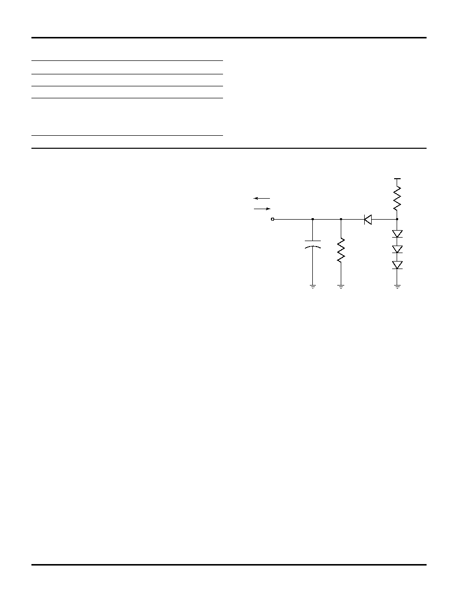
Figure 8. Test Load Diagram
From Output
Under Test
I
(+)
I
(≠)
30 pF
9.1 K
2.1 K
Z89223/273/323/373
ZiLOG
16-Bit Digital Signal Processors with A/D Converter
DS000202-DSP0599
17
DC ELECTRICAL CHARACTERISTICS
Table 7. OTP Version: V
DD
= 5V ±10%, T
A
= 0∞C to +70∞C for "S" temperature range
T
A
= ≠40∞C to +85∞C for "E" temperature range, unless otherwise noted;
IDD measured with peripherals disabled
Table 6. ROM Version: V
DD
= 5V ±10%, T
A
= 0∞C to +70∞C for "S" temperature range
T
A
= ≠40∞C to +85∞C for "E" temperature range, unless otherwise noted;
IDD measured with peripherals disabled
Symbol Parameter
Condition
Min
Typical Max
I
DD≠PLL
Supply Current using PLL
V
DD
= 5.0V, 20 MHz
60mA
66mA
I
DD≠ECD
Supply Current using External Clock Direct
V
DD
= 5.0V, 20 MHz
55 mA
61mA
I
DD≠XOD
Supply Current using XTAL Oscillator Direct
V
DD
= 5.0V, 32-kHz XTAL
250
µ
A
275
µ
A
I
DD≠DEEP
Supply Current during Deep Sleep
V
DD
= 5.0V, 32kHz XTAL
175
µ
A
193
µ
A
V
IH
Input High Level
2.7V
V
IL
Input Low Level
0.8V
I
L
Input Leakage
-10µA
10µA
V
OH
Output High Voltage
I
OH
= ≠100 µA
V
DD
≠0.2V
I
OH
= ≠160 µA
2.4V
V
OL
Output Low Voltage
I
OL
= 1.6 mA
0.4V
I
OL
= 2.0 mA
0.5V
I
FL
Output Floating Leakage Current
-10µA
10µA
Symbol Parameter
Condition
Min
Typical Max
I
DD≠PLL
Supply Current using PLL
V
DD
= 5.0V, 20 MHz
78mA
86mA
I
DD≠ECD
Supply Current using External Clock Direct
V
DD
= 5.0V, 20 MHz
75mA
83mA
I
DD≠XOD
Supply Current using XTAL Oscillator Direct
V
DD
= 5.0V, 32-kHz XTAL
17mA
19mA
I
DD≠DEEP
Supply Current during Deep Sleep
V
DD
= 5.0V, 32kHz XTAL
17mA
19mA
V
IH
Input High Level
2.7V
V
IL
Input Low Level
0.8V
I
L
Input Leakage
-10µA
10µA
V
OH
Output High Voltage
I
OH
= ≠100 µA
V
DD
≠0.2V
I
OH
= ≠160 µA
2.4V
V
OL
Output Low Voltage
I
OL
= 1.6 mA
0.4V
I
OL
= 2.0 mA
0.5V
I
FL
Output Floating Leakage Current
-10µA
10µA
Z89223/273/323/373
16-Bit Digital Signal Processors with A/D Converter
ZiLOG
18
DS000202-DSP0599
DC ELECTRICAL CHARACTERISTICS (Continued)
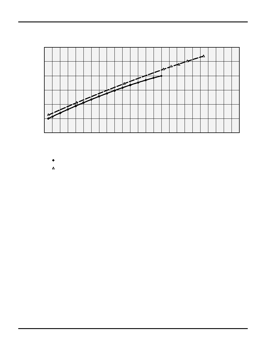
Figure 9. Z89373 Typical OTP Current Consumption
60
50
40
30
20
10
0
0
5
10
15
20
25
System Clock [MHz]
I [mA]
DD
Direct Clock with VCO Off
PLL Clock from 32.8KHz Crystal

Z89223/273/323/373
ZiLOG
16-Bit Digital Signal Processors with A/D Converter
DS000202-DSP0599
19
AC ELECTRICAL CHARACTERISTICS
Table 8. V
DD
= 5V ±10%, T
A
= 0∞C to +70∞C for "S" Temperature Range
T
A
= ≠40∞C to +85∞C for "E" temperature range, unless otherwise noted
Symbol
Parameter
Min [ns]
Max [ns]
Clock
TCY
CLKI Cycle Time for user-supplied clock
50
31250
CPWH
CLKI Pulse Width High
21
CPWL
CLKI Pulse Width Low
21
Tr
CLKI Rise Time for 20-MHz user-supplied clock
2
Tf
CLKI Fall Time for 20-MHz user-supplied clock
2
External Peripheral Bus
EASET
EA Setup Time to DS Fall
10
EAHOLD
EA Hold Time from DS Rise
4
RWSET
Read/Write Setup Time to DS Fall
10
RWHOLD
Read/Write Hold Time from DS Rise
0
RDSET
Data Read Setup Time to DS Rise
15
RDHOLD
Data Read Hold Time from DS Rise
0
WRVALID
Data Write Valid Time from DS Fall
5
WRHOLD
Data Write Hold Time from DS Rise
2
Reset
RRISE
Reset Rise Time
20 TCY
RWIDTH
Reset Low Pulse Width
2 TCY
Interrupt
IWIDTH
Interrupt Pulse Width
1TCY
Halt
HWIDTH
Halt Low Pulse Width
3 TCY
Wait State
WLAT
Wait Latency Time from DS Fall
7
WDEA
Wait Deassert Setup Time to CLKOUT Rise
TBD
SPI
SDI≠SCLK
Serial Data In to Serial Clock Setup Time
10
SCLK≠SDO
Serial Clock to Serial Data Out Valid
15
SS≠SCLK
Slave Select to Serial Clock Setup Time
1/2 SCLK Period
SS≠SDO
Slave Select to Serial Data Out Valid
15
SCLK≠SDI
Serial Clock to Serial Data In Hold Time
10
Z89223/273/323/373
16-Bit Digital Signal Processors with A/D Converter
ZiLOG
20
DS000202-DSP0599
8-BIT ANALOG/DIGITAL CONVERTER
Table 9. AV
CC
≠AGND = 5V ±10%
T
A
= 0∞C to +70∞C for "S" temperature range, unless otherwise noted
Parameter
Min
Typ
Max
Units
Integral Nonlinearity (INL)
0.5
1
LSB
Differential Nonlinearity (DNL)
0.5
1
LSB
Zero Offset Error
2
3
LSB
Full Scale Offset Error
2
3
LSB
Valid Input Signal Range
VALO
VAHI
V
Input Capacitance
33
40
pF
Conversion Time
2
3
µs
Input Impedance
500kSPS
100kSPS
44kSPS
10
48
110
k
k
k
VAHI
VALO + 2.5
AV
CC
V
VALO
AGND
AV
CC
–2.5
V
VAHI≠VALO
2.5
AV
CC
V
Reference Ladder Resistance
VAHI to VALO
5
k
Power Dissipation
50
85
mW
Table 10. AV
CC
≠AGND = 5V ±10%
T
A
= ≠40∞C to +85∞C for "E" temperature range, unless otherwise noted
Parameter
Min
Typ
Max
Units
Integral Nonlinearity (INL)
1
LSB
Differential Nonlinearity (DNL)
1
LSB
Zero Offset Error
3
4
LSB
Full Scale Offset Error
3
4
LSB
Valid Input Signal Range
VALO
VAHI
V
Input Capacitance
33
40
pF
Conversion Time
2
3
µs
Input Impedance
500kSPS
100kSPS
44kSPS
10
48
110
k
k
k
VAHI
VALO + 2.5
AV
CC
V
VALO
AGND
AV
CC
–2.5
V
VAHI≠VALO
2.5
AV
CC
V
Reference Ladder Resistance
VAHI to VALO
5
k
Power Dissipation
85
mW
Z89223/273/323/373
ZiLOG
16-Bit Digital Signal Processors with A/D Converter
DS000202-DSP0599
21
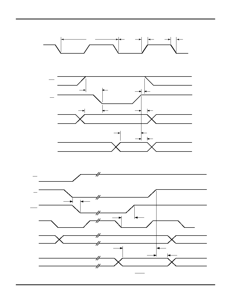
TIMING DIAGRAMS
Figure 10. Clock Timing
Figure 11. Read Timing
Figure 12. Read Timing Using WAIT Pin
TCY
CPWL
CPWH
T
T
r
f
EASET
RWSET
EAHOLD
RWHOLD
RDSET
RDHOLD
Data
Valid Address Out
DS
EA(2:0)
RD/WR
ED(15:0)
RDSET
WDEA
WLAT
RDHOLD
Valid Address Out
Data
WAIT
RD/WR
ED(15:0)
EA(2:0)
DS
CLKOUT
Z89223/273/323/373
16-Bit Digital Signal Processors with A/D Converter
ZiLOG
22
DS000202-DSP0599
TIMING DIAGRAMS (Continued)
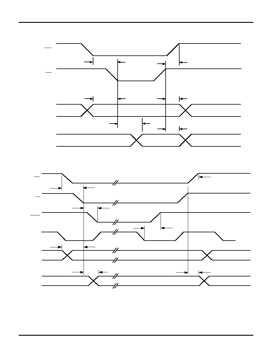
Figure 13. Write Timing
Figure 14. Write Timing Using WAIT Pin
EASET
RWSET
EAHOLD
RWHOLD
WRVALID
WRHOLD
Data
Valid Address Out
DS
EA(2:0)
RD/WR
ED(15:0)
WDEA
WLAT
EASET
WRHOLD
WRVALID
Valid Address Out
Data
WAIT
RD/WR
ED(15:0)
EA(2:0)
RWHOLD
DS
CLKOUT
RWSET
Z89223/273/323/373
ZiLOG
16-Bit Digital Signal Processors with A/D Converter
DS000202-DSP0599
23
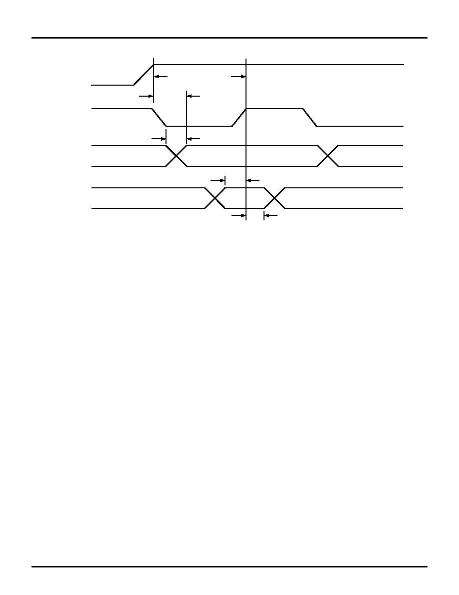
Figure 15. SPI Timing (Master and Slave Modes)
SDI-SCLK Setup
SCLK-SDI Hold
SS-SDO Valid
SS-SCLK Setup
Valid
Valid
SCLK*
SDO
SS*
SDI
SCLK-SDO Valid
TRI-STATE
*Notes: The polarity of SCLK and SS are programmable by the user. SS is used in Slave Mode only.
This figure illustrates data transmission on the falling edge of SCLK,
data reception on the rising edge of SCLK, with SS active Low (default).
Z89223/273/323/373
16-Bit Digital Signal Processors with A/D Converter
ZiLOG
24
DS000202-DSP0599
FUNCTIONAL DESCRIPTION
Instruction Timing.
Most instructions are executed in one
machine cycle. A multiplication or multiply/accumulate in-
struction requires a single cycle. Long immediate instruc-
tions, and Jump or Call instructions, are executed in two ma-
chine cycles. Specific instruction cycle times are described
in the Instruction Description section.
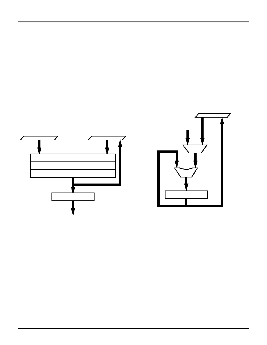
Multiply/Accumulate.
The multiplier can perform a 16-
bit x 16-bit multiply, or multiply/accumulate, in one ma-
chine cycle using the Accumulator and/or both the X and
Y inputs. The multiplier produces a 32-bit result, however,
only the 24 most significant bits are saved for the next in-
struction or accumulation. For operations on very small
numbers where the least significant bits are important, the
data should first be scaled to avoid truncation errors.
All inputs to the multiplier should be fractional two's-com-
plement, 16-bit binary numbers, which places them in the
range [≠1 to 0.9999695]. The result is in 24 bits, so the range
is [≠1 to 0.9999999].
If 8000H is loaded into both the X and Y registers, the mul-
tiplication produces an incorrect result. Positive one cannot
be represented in fractional notation, and the multiplier ac-
tually yields the result 8000H x 8000H = 8000H (≠1 x ≠1
= ≠1). The user should avoid this case to prevent erroneous
results.
A shifter between the P Register and the Multiplier Unit
Output can shift the data by three bits right or no shift.
Data Bus Bank Switch.
There is a switch that connects the
X Bus to the DDATA Bus that allows both the X and Y reg-
isters to be loaded with the same operand for a one cycle
squaring operation. The switch is also used to read the X
register.
ALU.
The ALU features two input ports. One is connected
to the output of the 24-bit Accumulator. The other input se-
lects either the Multiplier Unit Output or the 16-bit DDATA
bus (left-justified with zeros in the eight LSBs). The ALU
performs arithmetic, logic, and shift operations.
Hardware Stack.
A six-level hardware stack is connected
to the DDATA bus to hold subroutine return addresses or
data. The CALL instruction pushes PC+2 onto the stack,
and the RET instruction pops the contents of the stack to
the PC.
User Inputs and Outputs.
The Z893x3 features three
User Inputs, UI0, UI1, and UI2. Pins UI0 and UI1 are con-
nected directly to status register bits S10 and S11, and can
be read, or used as a condition code in any conditional in-
struction. Pins UI0, UI1 and UI2 may also be used to clock
the Counter/Timers. There are two user output bits, UO0
and UO1, which share pins with the timer outputs TMO0
and TMO1 on Port2. When the User Outputs are enabled,
they are the complements of bits S5 and S6 of the Status
Register.
Figure 16. Multiplier Block Diagram
MULTIPLIER
Shift Unit
Multiplier Unit
Output
16 MSB
P Register (24)
Y Register (16)
DDATA
16
24
XDATA
16
*Options:
No Shift
3 Bits Right
∑X Register (16)
Figure 17. ALU Block Diagram
Accumulator (24)
16 MSB
24
24
DDATA
Multiplier Unit
Output
16
24
24
MUX
ALU
Z89223/273/323/373
ZiLOG
16-Bit Digital Signal Processors with A/D Converter
DS000202-DSP0599
25
Interrupts.
The Z893x3 features three user interrupt inputs
which can be programmed to be positive or negative edge-
triggered. There are five interrupts generated by internal pe-
ripherals: the A/D converter, the Serial Peripheral Interface,
and the three Counter/Timers. Internally there are three pri-
ority levels. The internal signals for Interrupt service Re-
quests are denoted ISR0, ISR1, and ISR2, with ISR0 having
the highest priority, and ISR2 the lowest. The user can pro-
gram which interrupt sources are enabled, and which sourc-
es are serviced by the highest, middle, and lowest priority
service routines. An interrupt is serviced at the end of an
instruction execution. Two machine cycles are required to
enter an interrupt instruction sequence. The PC is pushed
onto the stack. The Interrupt Controller fetches the address
of the interrupt service routine from the following locations
in program memory:
At the end of the interrupt service routine, a RET instruction
is used to pop the stack into the PC.
The Set-Interrupt-Enable-Flag (SIEF) instruction enables
the interrupts. Interrupts are automatically disabled when
entering an interrupt service routine. Before exiting an in-
terrupt service routine the SIEF instruction can be used to
reenable interrupts.
Registers.
In addition to the internal registers for process-
ing, control, and configuration, the Z893x3 offers up to sev-
en user-defined 16-bit external registers, EXT0≠EXT6, de-
pending on the Register Bank Select value. The external
register address space is shared by the Z893x3 internal pe-
ripherals. Selecting banks 0≠4 of the EXT Register Assign-
ment allows access to/from three to seven of these addresses
for general-purpose use.
I/O Ports.
The Z893X3 DSP family features a user-config-
urable I/O structure. Most of the I/O pins include dual func-
tions. The Counter/Timer, Serial Peripheral Interface, and
External Interrupt Enables determine whether a pin is ded-
icated to peripheral or I/O port use.
Port0.
A 16-bit user I/O port. Bits can be configured as in-
put or output or globally as open-drain output. When en-
abled, Port0 consumes the 16 data lines used by the ED bus.
Port0 function and ED bus use can be dynamically alter-
nated by enabling and disabling Port0.
Port1.
A multifunctional 8-bit port. Bits can be configured
as input or output or globally as open-drain output. Port1
also supports INT2, CLKOUT, the Serial Peripheral Inter-
face, and User Inputs 0 and 1.
Port2.
A multifunctional 8-bit port. Bits can be configured
as input or output or globally as open-drain output. Port2
also supports INT0 and INT1, all three Counter/Timer out-
puts, ED Bus, WAIT, and UI2.
Port3.
Port3 is an 8-bit user I/O port with 4 bits of input and
4 bits of output. It is available only on the 80-pin package.
External Register Usage.
T h e e x t e r n a l r e g i s t e r s
EXT0≠EXT6 are accessed using the External Address Bus
EA2≠EA0, the External Data Bus (ED Bus) ED15≠ED0,
and control signals DS, WAIT, and RD/WR. These provide
a convenient data transfer capability with external periph-
erals. Data transfers can be performed in a single-cycle. An
internal wait state generator is provided to accommodate
slower external peripherals. A single wait state can be im-
plemented through control register Bank15/EXT3. For ad-
ditional wait states, the WAIT pin can be used. The WAIT
pin is monitored only during execution of a read or write
instruction to external peripherals on the ED bus.
Wait-State Generator.
An internal Wait-State generator
is provided to accommodate slow external peripherals. A
single Wait-State can be implemented through a control
register. For additional states, a dedicated pin (WAIT) can
be held Low. The WAIT pin is monitored only during ex-
ecution of a read or write instruction to external peripherals
(ED bus).
Analog to Digital Converter.
The A/D Converter is a 4-
channel, 8-bit half-flash converter. Two external reference
voltages provide a scalable input range. The A/D sample
rate is determined by a prescaler connected to the system
clock. An interrupt is optionally generated at the end of a
conversion. The four input channels can be programmed to
operate on demand, continuously, or upon an event (timer
or interrupt).
Counter/Timers (C/T0 and C/T1).
These C/Ts are 16-bit
with 8-bit prescalers. They also offer the option of being
used as PWM generators and include both hardware and
software Watch-Dog capabilities. Both C/Ts are identical
and can be externally or internally clocked. Either C/T can
drive TMO0 or TMO1. Either C/T can drive any of the three
interrupt service requests (ISR0, ISR1, or ISR2).
Counter/Timer (C/T2).
This C/T is 16-bits, externally or
internally clocked, and can drive TMO2 and/or any of the
three interrupt service requests (ISR0, ISR1, or ISR2).
Serial Peripheral Interface (SPI).
The Serial Peripheral
Interface provides a convenient means of inter-processor
and processor-peripheral communication. It offers the ca-
pability to transmit and receive simultaneously. The SPI is
designed to operate in either master or slave mode.
Device
ISR0
ISR1
ISR2
Z89223/273/323/373
1FFFH
1FFEH
1FFDH
Z89223/273/323/373
16-Bit Digital Signal Processors with A/D Converter
ZiLOG
26
DS000202-DSP0599
MEMORY MAP
Program Memory.
Programs of up to 8K words can be
masked into internal ROM (Z89323) or programmed into
OTP (Z89373). Four locations are dedicated to the vector
addresses for the three interrupt service routines
(1FFDH≠1FFFH) and for the starting address following a
RESET (1FFCH). Internal ROM is mapped from 0000H to
1FFFH, and the highest location for program instructions
is 1FFBH.
Internal Data RAM.
All Z893x3 family members feature
internal 512 x 16-bit data RAM organized as two banks of
256 x 16-bit words each (RAM0 and RAM1). The three ad-
dressing modes available to access the data RAM are direct
addressing, short form direct, and register indirect.
The contents of both data RAM banks can be read simul-
taneously and loaded into the X and Y inputs of the multi-
plier during a multiply instruction.
The addresses for each data RAM bank are:
0–255 (0000H–00FFH) for RAM0
256–511 (0100H–01FFH) for RAM1
Data RAM Pointers.
In register indirect, each data RAM
bank is addressed by one of three data RAM address point-
ers:
Example: Pn:b, where
n = pointer number = 0, 1, or 2
b = bank = 0 or 1,
thus,
P0:0, P1:0, P2:0 for RAM0
P0:1, P1:1, P2:1 for RAM1
In auto-increment, loop-increment, and loop-decrement in-
direct addressing, the pointer is automatically modified.
The data RAM pointers, which may be read or written di-
rectly, are 8-bit registers connected to the lower byte of the
internal 16-bit DDATA Bus.
Program Memory Pointers.
The first 16 locations of each
data RAM bank can be used as pointers to locations in Pro-
gram Memory. These pointers provide an efficient way to
address coefficients. The programmer selects a pointer lo-
cation using two bits in the status register and two bits in
the operand. At any one time, there are eight usable pointers,
four per bank, and the four pointers are in consecutive lo-
cations.
Example: Dn:b, where
n = pointer number = 0, 1, 2, or 3
b = bank = 0 or 1,
thus,
D0:0, D1:0, D2:0, D3:0 for RAM0
D0:1, D1:1, D2:1, D3:1 for RAM1
If S3/S4 = 01 in the status register, then
D0:0/D1:0/D2:0/D3:0 refer to register locations
4/5/6/7 in data RAM Bank 0.
Figure 18. Memory Map
Data Memory
Not Used
DRAM1
DRAM0
01FF
0100
00FF
0000
FFFF
Program Memory
Not Used
ISR0-ISR2 Vectors
RESET Vector
1FFF-D
1FFC
1FFB
0000
FFFF
FFFC
Or
8 KW
512 words
On-Chip Memory
On-Chip Memory
Z89223/273/323/373
ZiLOG
16-Bit Digital Signal Processors with A/D Converter
DS000202-DSP0599
27
REGISTERS
Both external and internal registers are accessed in one ma-
chine cycle. The external registers are used to access the on-
chip peripherals when they are enabled.
The internal registers of the Z893X3 are defined below:
X
and
Y
are two 16-bit input registers for the multiplier.
These registers can be utilized as temporary registers when
the multiplier is not being used.
P
holds the result of multiplications and is read-only.
A
is a 24-bit Accumulator. The output of the ALU is sent
to this register. When 16-bit data is transferred into this reg-
ister, it is placed into the 16 MSBs and the least significant
eight bits are set to zero. Only the upper 16 bits are trans-
ferred to the destination register when the Accumulator is
selected as a source register in transfer instructions.
Pn:b
are the pointer registers for accessing data RAM where
n = 0, 1, or 2, and b = 0 or 1. They can be directly read or
written. They point to locations in data RAM.
PC
is the Program Counter. Any instruction which may
modify this register requires two clock cycles.
SR
is the status register. It contains the ALU status and pro-
cessor control bits. The status register can always be read
in its entirety. S15≠S10 are set/reset by hardware and can
only be read by software. S9≠S0 control hardware opera-
tions and can be written by software.
Note: RO = read only, RW = read/write. The status register can
always be read in its entirety.
S15≠S12
are set/reset by the ALU after an operation.
S11≠S10
are set/reset by the user input pins.
If
S9
is set and a multiply/shift option is used, the shifter
shifts the result three bits right. This feature allows the data
to be scaled and prevents overflows.
If
S8
is set, the hardware clamps at maximum positive or
negative values instead of overflowing.
S7
enables interrupts.
S6≠S5
are User Outputs. The complement of the value in
the Status Register appears on bits 2 and 3 of Port2 if the
User Outputs are enabled by writing a 1 to Bit 15 of Bank
15≠EXT3, and Counter/Timer 0 and 1 are disabled.
S4≠S3
are the two MSBs in the "short form direct" mode
of addressing.
S2≠S0
define the RAM pointer loop size as indicated in Ta-
ble 12.
Register Register
Definition
X
Multiplier X Input, 16-bits
Y
Multiplier Y Input, 16-bits
P
Multiplier Output, 24-bits
A
Accumulator, 24-bits
Pn:b
Six Data RAM Pointers, 8-bits each
PC
Program Counter, 16-bits
SR
Status Register, 16-bits
EXT0
depends on Bank Select #, 16-bits
EXT1
depends on Bank Select #, 16-bits
EXT2
depends on Bank Select #, 16-bits
EXT3
depends on Bank Select #, 16-bits
EXT4
depends on Bank Select #, 16-bits
EXT5
depends on Bank Select #, 16-bits
EXT6
depends on Bank Select #, 16-bits
EXT7
Interrupt Status/Bank Select, 16-bits
Table 11. Status Register Bit Functions
SR Bit
Function
Read/Write
S15 (N)
ALU Negative
RO
S14 (OV)
ALU Overflow
RO
S13 (Z)
ALU Zero
RO
S12 (C)
Carry
RO
S11 (UI1)
User Input 1
RO
S10 (UI0)
User Input 0
RO
S9 (SH3)
MPY Output
Arithmetically Shifted
Right by Three Bits
R/W
S8 (OP)
Overflow Protection
R/W
S7 (IE)
Interrupt Enable
R/W
S6 (UO1)
User Output 1
R/W
S5 (UO0)
User Output 0
R/W
S4≠S3
"Short Form Direct" bits R/W
S2≠S0 (RPL)
RAM Pointer Loop Size
R/W
Z89223/273/323/373
16-Bit Digital Signal Processors with A/D Converter
ZiLOG
28
DS000202-DSP0599
REGISTERS (Continued)
The following are not actually registers, but are read or writ-
ten in the same way as hardware registers on the chip:
BUS
is a read-only register which, when accessed, returns
the contents of the D-Bus. BUS is used for emulation only.
Dn:b
refers to locations in RAM that can be used as a pointer
to locations in program memory which is efficient for co-
efficient addressing. The programmer decides which loca-
tion to choose from two bits in the status register and two
bits in the operand. Thus, only the lower 16 possible loca-
tions in RAM can be specified. At any one time, there are
eight usable pointers, four per bank, and the four pointers
are in consecutive locations in RAM. For example, if
S3/S4=01 in the status register, then D0:0/D1:0/D2:0/D3:0
refer to register locations 4/5/6/7 in RAM Bank 0. Note that
when the data pointers are being written to, a number is ac-
tually being loaded to Data RAM, so they can be used as a
limited method for writing to RAM.
EXTn
are external registers (n = 0 to 6). These are seven
16-bit register addresses provided for mapping internal and
external peripherals into the address space of the processor.
Note that for external peripherals the actual register RAM
does not exist on the chip, but would exist as part of the ex-
ternal device, such as an A/D result latch. The External Ad-
dress Bus, EA2≠EA0, the External Data Bus, ED15≠ED0,
DS, WAIT, and RD/WR are used to access external periph-
erals.
EXT7
is used for Register Bank Select, and to program wait
states for EXT0≠EXT6, and is not available for accessing
an external peripheral.
Table 12. RPL Description
S2
S1
S0
Loop Size
0
0
0
256
0
0
1
2
0
1
0
4
0
1
1
8
1
0
0
16
1
0
1
32
1
1
0
64
1
1
1
128
Register
Register Definition
BUS
D-Bus
Dn:b
Eight Data Pointers
EXTn
External Register, 16-bit
Figure 19. Status Register
0 0 0
0 0 1
0 1 0
0 1 1
1 0 0
1 0 1
1 1 0
1 1 1
256
2
4
8
16
32
64
128
"Short Form Direct" bits
User Output UO1, UO0
(Complemented)
Global Interrupt Enable
Overflow Protection
MPY output arithmetically
shifted right by three bits
User Input UI1,UI0
(Read Only)
Carry
Zero
Overflow
Negative
Ram
Pointer
Loop
Size
S7
S6
S5
S4
S3
S2
S1
S0
S15
S14
S13
S12
S11
S10
S9
S8
N
OV
Z
C
UI1
UI0
SH3
OP
IE
UO1 UO0
RPL

Z89223/273/323/373
ZiLOG
16-Bit Digital Signal Processors with A/D Converter
DS000202-DSP0599
29
BANK/EXT REGISTER ASSIGNMENTS
There are 16 different Banks of EXT registers. Control of
the bank switching is done via the EXT7 register. The same
EXT7 register exists in all Banks.
Banks 0≠5 support different combinations of external reg-
isters for external peripherals, and external registers for in-
ternal (on-chip) peripherals. Use the bank that offers the op-
timum combination of internal and external registers to
support the application. Use it as a preferred working bank
to minimize bank switching.
Banks 6≠12 only decode EXT6 and EXT7. Do not use
EXT0≠5 for Banks 6≠12.
Banks 13≠15 are control register banks. These banks are
used in the initialization routines and whenever a configu-
ration change is required. Refer to the sections on I/O Ports
and Peripherals for details.
Table 13. EXT Register Assignments Banks 0≠4
Bank0
Bank1
Bank2
Bank3
Bank4
EXT0
User
User
User
User
User
EXT1
User
User
User
User
User
EXT2
User
User
User
User
User
EXT3
SPI Data
User
User
SPI Data
User
EXT4
Port0 Data
Port0 Data
User
User
User
EXT5
Port2≠Port1 Data
Port2≠Port1 Data
Port3 Data
User
User
EXT6
A/D_Ch0 Data
A/D_Ch1 Data
A/D_Ch2 Data
A/D_Ch3 Data
User
EXT7
Interrupt status/
Bank Select
Interrupt status/
Bank Select
Interrupt status/
Bank Select
Interrupt status/
Bank Select
Interrupt status/
Bank Select
Table 14. EXT Register Assignments Banks 5≠15
Bank5
Bank6≠12
Bank13
Bank14
Bank15
EXT0
A/D_Ch1 Data
not defined
A/D Control
C/T2 Load/Read
Port0 Control
EXT1
A/D_Ch2 Data
not defined
C/T0 Control
C/T1 Control
Port1 Ctrl/Port0 Alloc
EXT2
A/D_Ch3 Data
not defined
C/T0 Load
C/T1 Load
Ports 2, 3, & C/T2
Control
EXT3
SPI Data
not defined
C/T0 Counter
C/T1 Counter
Wait State Control
EXT4
Port0 Data
not defined
C/T0 Prescaler Ld C/T1 Prescaler Ld SPI Control
EXT5
Port2≠Port1 Data
not defined
C/T0 Prescaler
C/T1 Prescaler
System Clock Control
EXT6
A/D_Ch0 Data
A/D_Ch0 Data
A/D_Ch0 Data
Interrupt Polarity
Interrupt Allocation
EXT7
Interrupt status/
Bank Select
Interrupt status/
Bank Select
Interrupt status/
Bank Select
Interrupt status/
Bank Select
Interrupt status/
Bank Select
Z89223/273/323/373
16-Bit Digital Signal Processors with A/D Converter
ZiLOG
30
DS000202-DSP0599
BANK/EXT REGISTER ASSIGNMENTS (Continued)
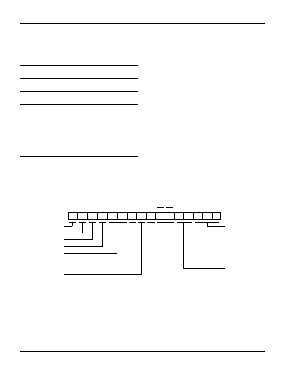
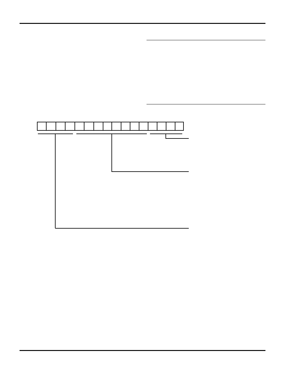
Interrupt Status/Bank Select Register—EXT7
Following is a description of EXT7. It contains both a Bank
Select Field and Interrupt Status Bits.
Bank Select Field.
The four LSBs of EXT7 denote which
bank is selected as the current working bank.
Interrupt Status Bits.
These bits can be read to identify
which interrupts are pending. A "1" denotes interrupt pend-
ing, and a "0" denotes no interrupt. This ability to identify in-
terrupts is particularly useful in polled interrupt operation or
when servicing ISR2, which may come from several sources.
Note: Write "1" to a particular status bit to clear that bit. Before
exiting an interrupt service routine, the relevant interrupt
bit(s) should be cleared. To clear a bit efficiently:
∑ Load the value of EXT7 into a register or memory
location
∑ Then load that value back into EXT7
Performing these steps clear all of the interrupts that
were pending, but leave the Register Bank Select
unchanged.
Figure 20. EXT7 Register
Interrupt Status Bits
Bit 4 = A/D Finish Interrupt
Bit 5 = SPI Interrupt
Bit 6 = Timer0 Interrupt
Bit 7 = Timer1 Interrupt
Bit 8 = Timer2 Interrupt
Bit 9 = INT0 (H/W) Interrupt
Bit 10 = INT1 (H/W) Interrupt
Bit 11 = INT2 (H/W) Interrupt
Bank Select
0000 : Bank0
0001 : Bank1
:
:
1111 : Bank15
Reserved
Ext 7 Reg
D15 D14 D13 D12 D11 D10
D9
D8
D7
D6
D5
D4
D3
D2
D1
D0
Z89223/273/323/373
ZiLOG
16-Bit Digital Signal Processors with A/D Converter
DS000202-DSP0599
31
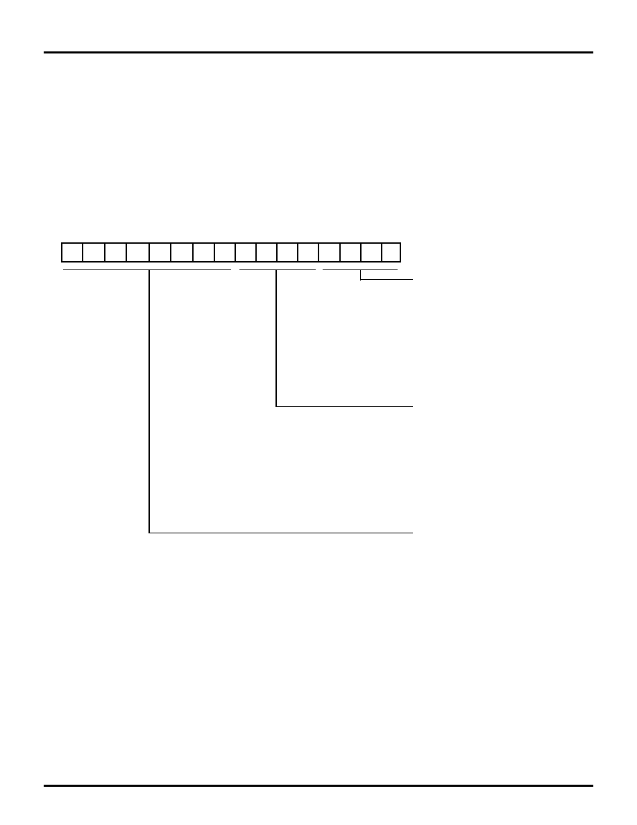
Interrupt Allocation Register
—
Bank15/EXT6
Bits 3≠0 of the Interrupt Allocation Register define which
unique interrupt source the highest priority, and is allocated
to ISR0 (Interrupt Service Request 0).
Bits 7≠4 of the Interrupt Allocation Register define which
unique interrupt source has the second highest priority, and
is allocated to ISR1 (Interrupt Service Request 1).
Bits 15≠8 of the Interrupt Allocation Register are enable bits
for common interrupt sources which have the lowest prior-
ity, and are all allocated to ISR2 (Interrupt Service Request
2). All the enabled interrupts which are not allocated to ISR0
or ISR1, are allocated to ISR2. When an ISR2 interrupt oc-
curs, the interrupt service routine must read the Interrupt
Status Register in EXT7 to determine the source. The In-
terrupt Status Register can be used for polling interrupts.
An Interrupt that is not selected as a source to ISR0, ISR1,
or ISR2, is disabled.
Figure 21. Interrupt Allocation Register
ISR0 Source (highest priority)
D7
D6 D5
D4
D3
D2
D1 D0
D15 D14 D13 D12 D11 D10 D9
D8
Bank 15/EXT6
0000 = A/D
0001 = SPI
0010 = C/T0
0011 = C/T1
0100 = C/T2
0101 = INT0
0110 = INT1
0111 = INT2
1xxx = ISR0 Disabled
ISR1 Source (medium priority)
0000 = A/D
0001 = SPI
0010 = C/T0
0011 = C/T1
0100 = C/T2
0101 = INT0
0110 = INT1
0111 = INT2
1xxx = ISR0 Disabled
ISR2 Interrupt Source (lowest priority)
1 = Enable, 0 = Disable
Bit 8 = A/D
Bit 9 = SPI
Bit 10 = C/T0
Bit 11 = C/T1
Bit 12 = C/T2
Bit 13 = INT0
Bit 14 = INT1
Bit 15 = INT2
Z89223/273/323/373
16-Bit Digital Signal Processors with A/D Converter
ZiLOG
32
DS000202-DSP0599
BANK/EXT REGISTER ASSIGNMENTS (Continued)
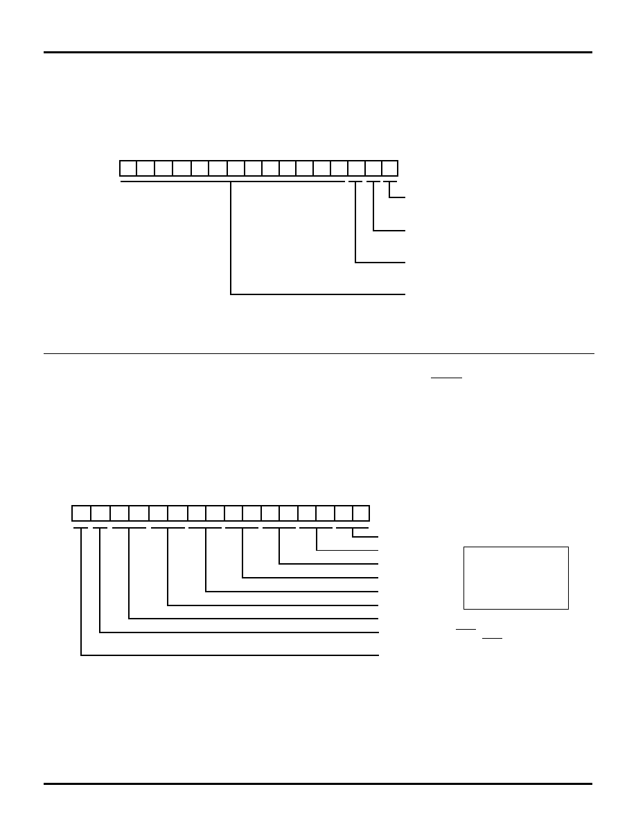
Interrupt Polarity Register
—
Bank14/EXT6
The trigger polarities, rising-edge or falling-edge, of all the
external interrupts are programmable.
Wait-State Control Register—Bank15/EXT3
The Wait-State Control Register enables the insertion of
wait states when the DSP accesses slow peripherals. This
register enables the insertion of one wait state on the ED
bus, providing 100 ns of access time instead of 50 ns when
operating at 20 MHz. When more than one wait state is nec-
essary, input pin P2.4/ WAIT can be used to provide addi-
tional wait states. The Wait-State Register enables the user
to specify which EXT registers, EXT0≠EXT6, and which
operation, read and/or write, require a wait state. EXT7 is
an internal register, and requires no wait state.
Figure 22. Interrupt Polarity Register
D7
D6
D5
D4
D3
D2
D1 D0
D15 D14 D13 D12 D11 D10
D9
D8
Bank 14/Ext 6 Reg
INT0 Polarity
0 : Rising Edge (default)
1 : Falling Edge
INT1 Polarity
0 : Rising Edge (default)
1 : Falling Edge
INT2 Polarity
0 : Rising Edge (default)
1 : Falling Edge
Bits [15:3]--Reserved
Figure 23. Wait-State Control Register
D7
D6
D5
D4
D3
D2
D1
D0
D15 D14 D13 D12 D11 D10
D9
D8
Bank15/EXT3 Reg
Wait-State EXT6
Wait-State EXT0
Bit14: 0 = Disabled WAIT Input Pin (default)
1 = Enabled P2.4 as WAIT Input Pin
Bit 15: 0 = Disabled UO0, UO1 (default)
1 = Enable UO0, UO1
Wait-State EXT5
Wait-State EXT4
Wait-State EXT3
Wait-State EXT2
Wait-State EXT1
00 = read (nws), write (nws)
01 = read (nws), write (nws)
10 = read (ws), write (ws)
11 = read (ws), write (ws)
nws = no wait state
ws = one wait state
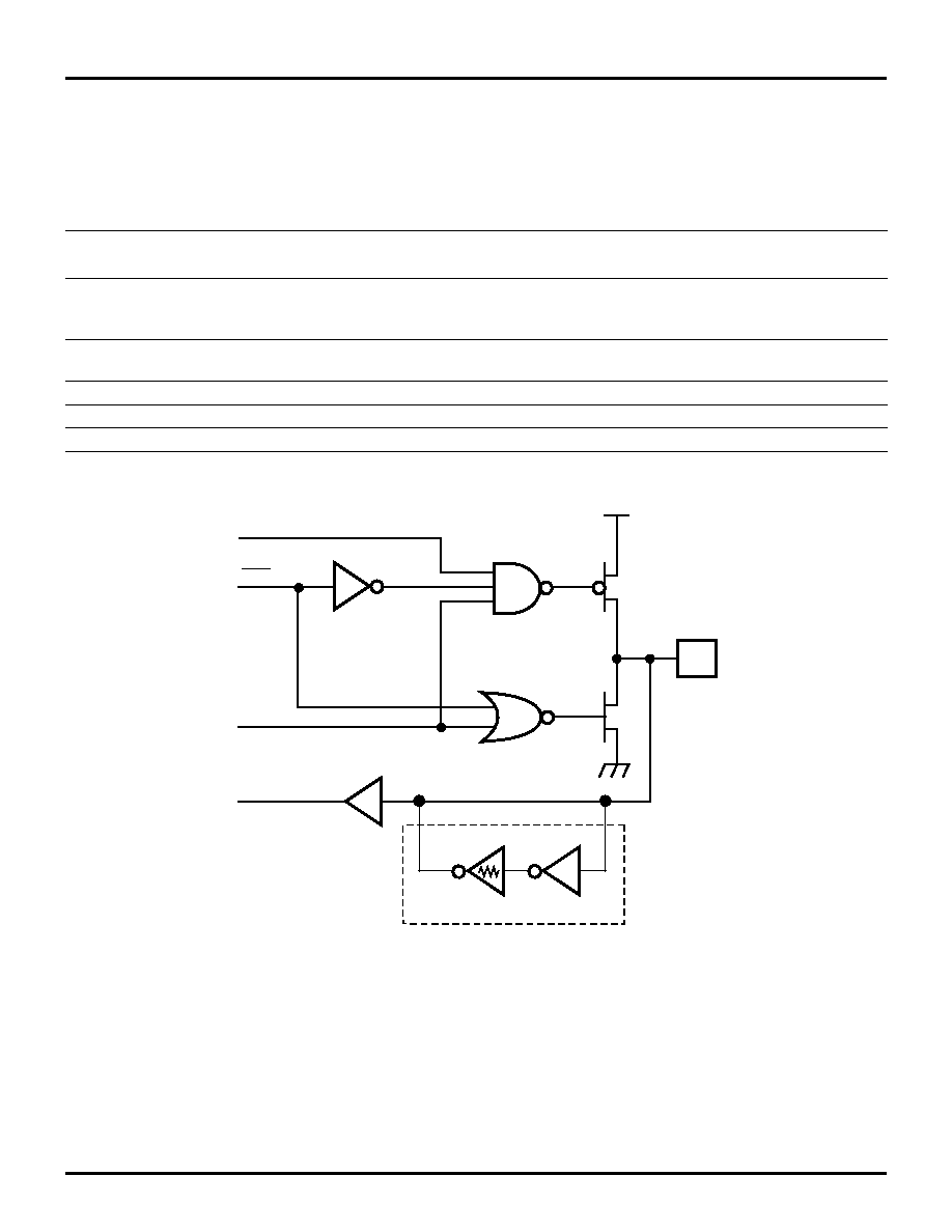
Z89223/273/323/373
ZiLOG
16-Bit Digital Signal Processors with A/D Converter
DS000202-DSP0599
33
I/O PORTS
I/O pin allocation of ports for the different package types
is designed to provide configuration flexibility. Each port
line of Ports 0, 1, and 2 can be independently selected as
an input or an output. Each port's output lines can be glo-
bally selected as push-pull or as open-drain outputs
Table 15. I/O Port Bit Allocations
Device Pins
44-Pin PLCC,
44-Pin PQFP
64-Pin TQFP,
68-Pin PLCC
80-Pin PQFP
P0 MSB
ED15≠ED8, or
P0.15≠P0.8, or
P1.7≠P1.0
ED15≠ED8, or
P0.15≠P0.8
ED15≠ED8, or
P0.15≠P0.8
P0 LSB
ED7≠ED0, or
P0.7≠P0.0
ED7≠ED0, or
P0.7≠P0.0
ED7≠ED0, or
P0.7≠P0.0
P1
P1.7≠P1.0
P1.7≠P1.0
P2
P2.4≠P2.0
P2.7≠P2.0
P2.7≠P2.0
P3
P3.7≠P3.0
Figure 24. Port 0, 1 and 2 Configuration
OEN
Open-Drain
Data Out
Data In
PAD
Auto Latch
R
500 k
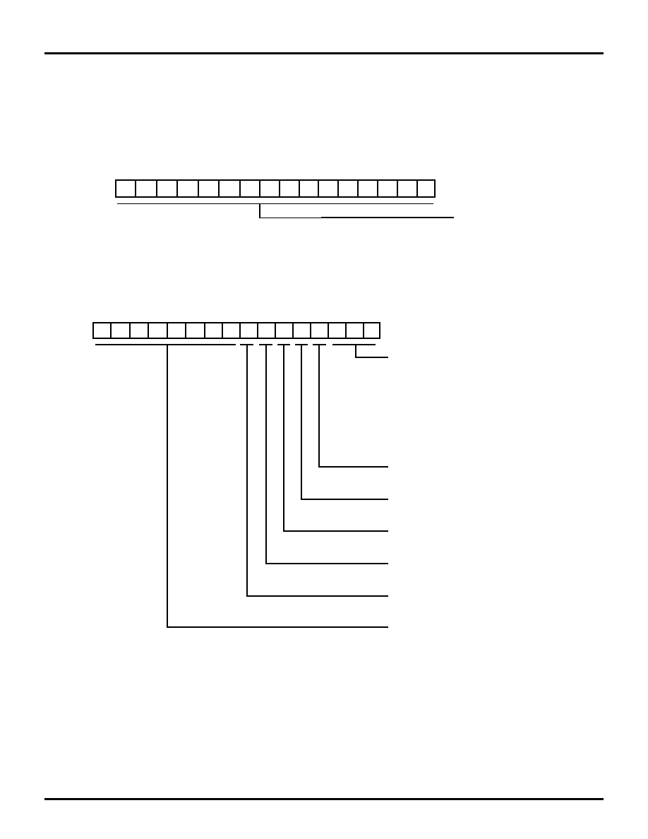
Z89223/273/323/373
16-Bit Digital Signal Processors with A/D Converter
ZiLOG
34
DS000202-DSP0599
I/O PORTS (Continued)
Port0—16-Bit Programmable I/O
Bank15/EXT0 is the Port0 direction control register.
Bank15/EXT1 includes specific bits to enable and config-
ure Port0. The Port0 data register is Ext4 in Banks 0, 1, or 5.
Figure 25. Port 0 Control Register
Figure 26. Bank15/EXT1 Register
Port I/O Direction
0 = Input (default)
1 = Output
D7
D6
D5
D4
D3
D2
D1
D0
D15 D14 D13 D12 D11 D10
D9
D8
Bank 15/Ext 0 Reg
D7
D6
D5
D4
D3
D2
D1
D0
D15 D14 D13 D12 D11 D10 D9
D8
Bank 15/EXT1
INT2
0 = Disabled (default)
1 = Enabled
INT1
0 = Disabled (default)
1 = Enabled
CLKOUT
0 = Disabled (default)
1 = Enabled
Port1 Outputs
0 = Push-Pull (default)
1 = Open-Drain
Port I/O Output Bit Directions
0 = Input (default)
1 = Output
Port0 Outputs
0 = Push-Pull (default)
1 = Open-Drain
Allocation of External Data (ED) Bus/Port0 Pins
000 = ED Bus 15-0 (default)
001 = Pins 15≠8
P1.7≠P1.0,
Pins 7≠0
ED Bus 7≠0
010 = Reserved
011 = Pins 15≠8
P0.15≠P08,
Pins 7≠0
ED Bus 7≠0
100 = P0.15≠P0.0
101 = Pins 15≠8
P1.7≠P1.0
Pins 7≠0
P0.7≠P0.0
110 = Reserved
111 = Reserved
Z89223/273/323/373
ZiLOG
16-Bit Digital Signal Processors with A/D Converter
DS000202-DSP0599
35
Port1—8-Bit Programmable I/O
Bank15/EXT1 is the Port1 control register. The MSB is the
Port1 direction control. Port1 data is accessed as the LSB
of EXT5 in Banks 0, 1, or 5. The Port1 pins can also be
mapped to internal functions. When INT2, CLKOUT, UI0
and UI1, or the SPI are enabled, they use Port1 pins. The
44-pin packages do not feature Port1 pins, however, Port1
and its internal functions can be mapped to the MSB of the
ED Bus/Port0 pins. See bits 2≠0 of Bank15/EXT1.
Table 16. Port1 Bit Function Allocation
Port Pin
IF
Condition
Then
Else
P1.0/INT2
Bank15/EXT1 Bit 3 = 1
Enable INT2
INT2
P1.0
P1.1/CLKOUT
Bank15/EXT1 Bit 5 = 1
Enable CLKOUT
CLKOUT
P1.1
P1.2/SDI
Bank15/EXT4 Bit 0 = 1
Enable SPI
SDI
P1.2
P1.3/SDO
Bank15/EXT4 Bit 0 = 1
Enable SPI
SDO
P1.3
P1.4/SS
Bank15/EXT4 Bit 0 = 1
Enable SPI
SS
P1.4
P1.5/SCLK
Bank15/EXT4 Bit 0 = 1
Enable SPI
SCLK
P1.5
P1.6/UI0
Bank13/EXT1 Bits [2,1] = 10, or
Bank14/EXT1 Bits [2,1] = 10
Enable UI0
UI0
P1.6
P1.7/UI1
Bank13/EXT1 Bits [2,1] = 11, or
Bank14/EXT1 Bits [2,1] = 11
Enable UI1
UI1
P1.7
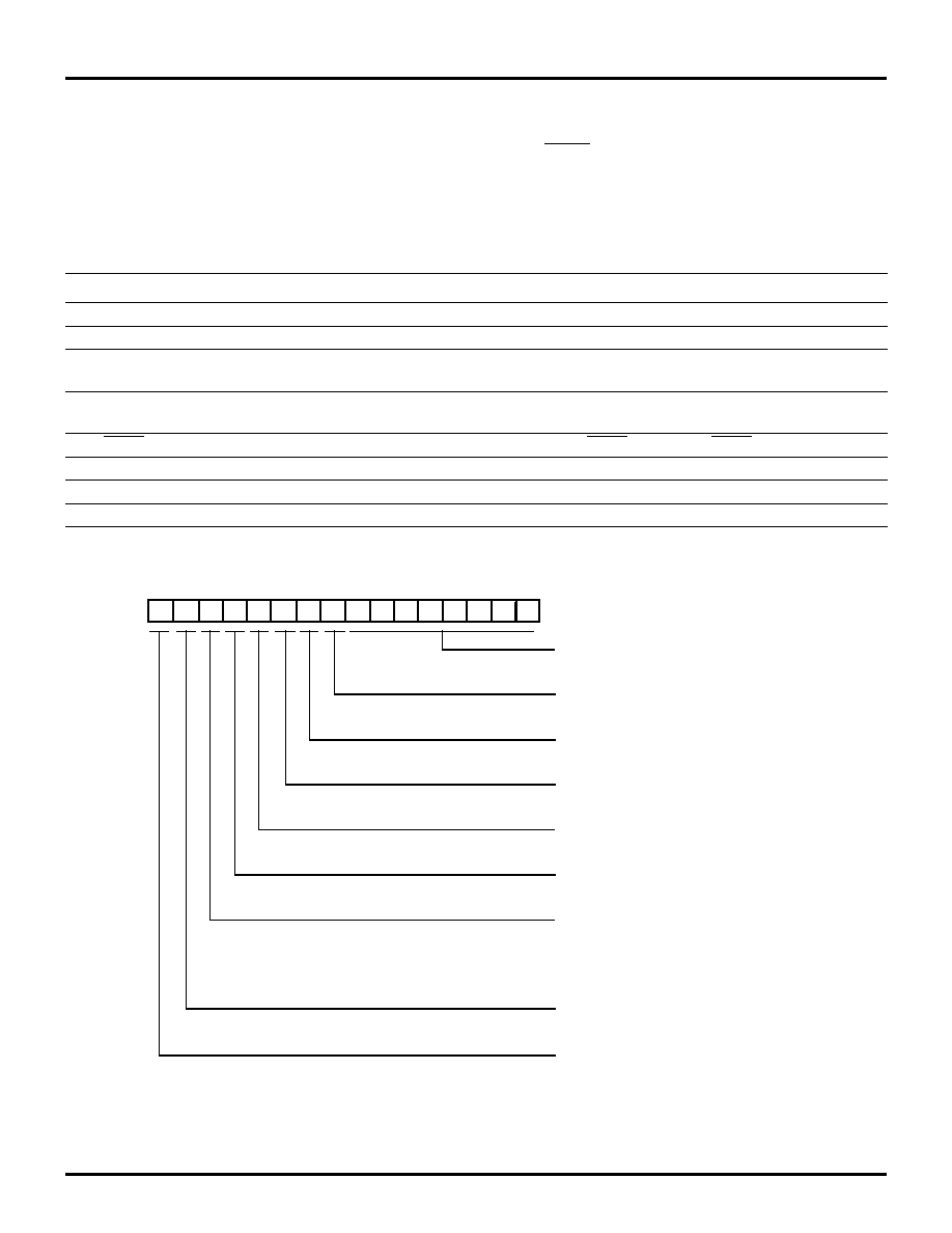
Z89223/273/323/373
16-Bit Digital Signal Processors with A/D Converter
ZiLOG
36
DS000202-DSP0599
I/O PORTS (Continued)
Port2—8-Bit Programmable I/O
Bank15/EXT2 is the Port2 control register. The LSB is the
Port2 direction control. Port2 data is accessed as the MSB
of EXT5 in Banks 0,1,or 5. The Port2 pins can also be
mapped to internal functions. When INT0, INT1, TMO0,
TMO1, WAIT, UI2, or TMO2 are enabled, they use Port2
pins. The 44-pin packages do not feature Port2 pins
P2.7≠P2.5.
Table 17. Port2 Bit Function Allocation
Port Pin
IF
Condition
Then
Else
P2.0/INT0
Bank15/EXT2 Bit 9 = 1
Enable INT0
INT0
P2.0
P2.1/INT1
Bank15/EXT1 Bit 4 = 1
Enable INT1
INT1
P2.1
P2.2/TMO0
Bank13/EXT1 Bit [6,5] = 10, or
Bank14/EXT1 Bit [6,5] = 10
Enable TMO0
TMO0
P2.2
P2.3/TMO1
Bank13/EXT1 Bit [6,5] = 11, or
Bank14/EXT1 Bit [6,5] = 11
Enable TMO1
TMO1
P2.3
P2.4/WAIT
Bank15/EXT3 Bit 14 = 1
Enable WAIT
WAIT
P2.4
P2.5/UI2
Bank15/EXT2 Bit 13 = 1
C/T2 clock is UI2
UI2
P2.5
P2.6/TMO2
Bank15/EXT2 Bits 14 = 1
Enable TMO2
TMO2
P2.6
P2.7
P2.7
P2.7
Figure 27. Bank15/EXT2 Register
D7 D6
D5 D4 D3
D2 D1
D0
D15 D14 D13 D12 D11 D10 D9
D8
Bank 15/EXT2
Port2 I/O Directions
0 = Input (default)
1 = Output
Port3
0 = Disabled (default)
1 = Enabled
INT0
0 = Disabled (default)
1 = Enabled
Port2 Outputs
0 = Push-Pull (default)
1 = Open-Drain
Counter/Timer2
0 = Disabled (default)
1 = Enabled
Counter/Timer2 Operation
0 = Stopped (default)
1 = Counting
If D15 = 0, Counter/Timer2 Clock defined by
0 = System Clock/2 (default)
1 = UI2
If D15 = 1, Counter/Timer2 Sleep Mode Wake-Up
0 = Disabled (default)
1 = Enabled
TMO2
Counter/Timer2 Clock
0 = Disabled (default)
1 = Enabled
0 = Defined by D13 (default)
1 = CLKI

Z89223/273/323/373
ZiLOG
16-Bit Digital Signal Processors with A/D Converter
DS000202-DSP0599
37
Port3—8-BIt Programmable I/O
Port3 is an additional I/O port available only in the 80-pin
package. P3.3≠P3.0 are inputs and P3.7≠P3.4 are outputs.
Bit 8 of Bank15/EXT2 enables and disables Port3. The LSB
of Bank2/EXT5 is the Port3 Data Register.
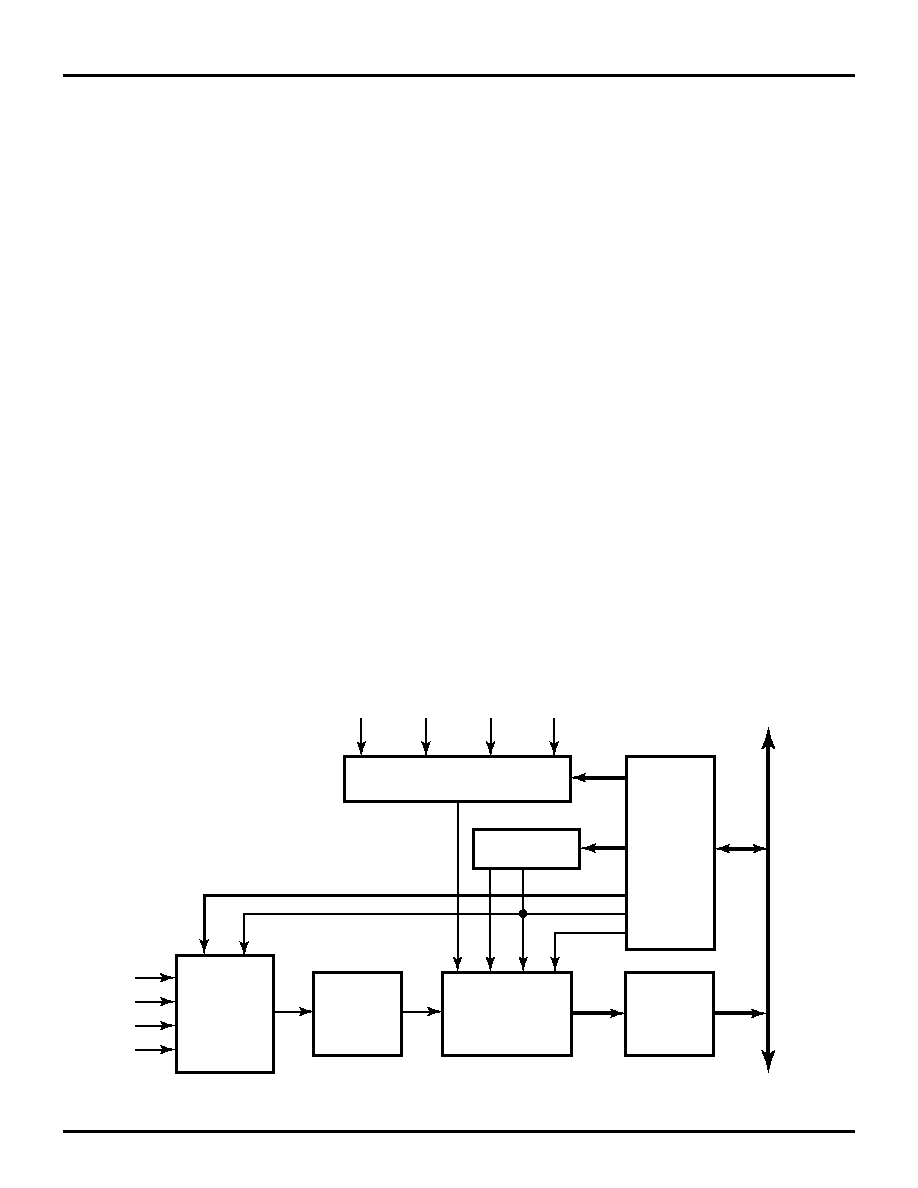
Z89223/273/323/373
16-Bit Digital Signal Processors with A/D Converter
ZiLOG
38
DS000202-DSP0599
PERIPHERALS
Analog to Digital Converter (A/D)
The A/D is a 4-channel 8-bit half-flash converter. It uses
two reference resistor ladders, one for the upper 5 bits, and
another for the lower 3 bits. Two external reference voltage
input pins, VAHI and VALO, set the input voltage mea-
surement conversion range. The converter is auto-zeroed
prior to each sampling period. Bank13/EXT0 is the A/D
control register.
The conversion time depends on the system clock frequency
and the selection of the A/D prescaler value, bits
DIV2≠DIV0. The clock prescaler can be programmed to de-
rive a 2 µs conversion time. For example, when deriving
the A/D clock from a 20-MHz system clock, the A/D pres-
caler value should be set to divide by 40.
Bits ADST1≠ADST0 determine one of the following start
conversion options:
∑
Writing to the ADCTL control register
∑
ISR1
∑
C/T2 time-out
∑
C/T0 time-out
The start conversion operation may begin at any time. If a
conversion is in progress, and a new start conversion signal
is received, the conversion in progress will abort, and a new
conversion will initiate.
Bits QUAD and SCAN determine one of the following
Modes of operation:
∑
One channel is converted four times, with the results se-
quentially written to result registers 0, 1, 2 and 3.
∑
One channel is converted one time, with the respective
result register updated.
∑
Four channels are converted one time each, with the re-
spective four result registers updated.
∑
Four channels are converted repeatedly, with the respec-
tive four result registers constantly updated.
When one of the two four-channel modes is selected, the
channel specified by CSEL1≠CSEL0 will convert first. The
other three channels will convert in sequence. In the se-
quence, AN0 follows AN3.
Bit ADIE enables the A/D to generate interrupts at the end
of a conversion. Bit ADIT determines whether an interrupt
occurs after the first or fourth conversion.
To reduce power consumption the A/D can be disabled by
clearing the ADE bit.
Though the A/D will function with smaller input signals and
reference voltages, the noise and offsets remain constant.
The relative error of the converter will increase and the con-
version time will also take longer.
Figure 28. ADC Architecture
Internal
Bus
Channel Select
4x8
Result
Register
A/D
Control
Register
Half-Flash
A/D
Converter
Sample
and
Hold
4-Channel
Multiplexer
A/D
Prescaler
Start
Converter
ISR1
C/T0
C/T2
ADCTL Reg.
Scan
Quad
AN0
AN1
AN2
AN3
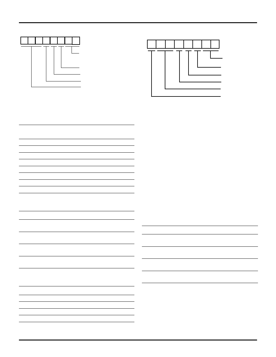
Z89223/273/323/373
ZiLOG
16-Bit Digital Signal Processors with A/D Converter
DS000202-DSP0599
39
ADE (Bit 15).
A "0" disables any A/D conversions or ac-
cessing any A/D registers, except writing to the ADE bit.
A "1" enables all A/D accesses.
Reserved (Bits 14, 13).
Reserved for future use.
ADCINT (Bit 12).
The A/D interrupt bit is read-only. The
ADCINT will reset every time this register is written.
ADIT (Bit 11).
Selects when to set the A/D interrupt if in-
terrupts are enabled (ADIE=1). A value of "0" sets the in-
terrupt after the first A/D conversion is complete. A value
of "1" sets the interrupt after the fourth A/D conversion is
complete.
ADIE (Bit 10).
A/D Interrupt Enable. A value of "0" dis-
ables the A/D Interrupt. A value of "1" enables the A/D In-
terrupt.
There are four A/D result registers. See the EXT Register
Assignments for their location in the different banks.
Figure 29. ADCTL Register (LSB)
Table 18. A/D Prescaler Values (Bits 7, 6, 5)
DIV2
DIV1
DIV0
A/D Prescaler
(Crystal divided by)
0
0
0
8
0
0
1
16
0
1
0
24
0
1
1
32
1
0
0
40
1
0
1
48
1
1
0
56
1
1
1
64
Table 19. Operating Modes (Bits 4, 3)
QUAD
SCAN
Option
0
0
Convert selected channel 4 times,
then stop
0
1
Convert selected channel,
then stop.
1
0
Convert 4 channels,
then stop.
1
1
Convert 4 channels
continuously.
Table 20. Channel Select (Bits 1, 0)
CSEL1
CSEL0
Channel
0
0
AN0
0
1
AN1
1
0
AN2
1
1
AN3
DIV0
Bank13/EXT0 (LSB)
DIV1
DIV2
CSEL0
CSEL1
(Reserved)
SCAN
QUAD
D7 D6 D5 D4 D3 D2 D1 D0
Figure 30. ADCTL Register (MSB)
Table 21. START (Bits 9, 8)
ADST1
ADST0
Option
0
0
Conversion starts when this
register is written.
0
1
Conversion starts on INT1 per
Interrupt Allocation Register
1
0
Conversion starts on C/T2
time-out.
1
1
Conversion starts on C/T0
time-out.
ADST0
ADST1
D15 D14 D13 D12 D11 D10 D9 D8
ADIE
(Reserved)
Bank13/EXT0 (MSB)
ADE
ADCINT
ADIT

Z89223/273/323/373
16-Bit Digital Signal Processors with A/D Converter
ZiLOG
40
DS000202-DSP0599
PERIPHERALS (Continued)
Counter/Timers (C/T0 and C/T1)
The Z893x3 features two 16-bit Counter/Timers (C/T) that
can be independently configured to operate in various
modes. Each is implemented as a 16-bit Load Register and
a 16-bit down counter. Either C/T input can be selected from
UI0 or UI1. Either C/T output can be directed to TMO0 or
TMO1. The C/T clock is a scaled version of the system
clock. Each C/T features an 8-bit prescaler. The clock rates
of the two C/T are independent of each other. The C/Ts can
be programmed to recognize clock events on the rising
edge, the falling edge, or both rising and falling edges of
the input signal. Outputs on TMO0 or TMO1 can be pro-
grammed to occur with either polarity.
If either C/T is enabled and an output pin TMO0 or TMO1
is selected, and at the same time User Outputs are enabled,
the C/T takes precedence, and Status Register bits 5 or 6
do not affect the state of the selected pin.
C/T Modes of Operation:
MODE 0--Square Wave Output.
The C/T is configured
to generate a continuous square wave of 50% duty cycle.
Writing a new value to the TMLR Register takes effect at
the end of the current cycle, unless TMR is written.
MODE 1--Retriggerable One-Shot.
The C/T is config-
ured to generate a single pulse of programmable duration.
The pulse may be either logic High or logic Low. Retrig-
gering the one-shot before the end of the pulse causes it to
retrigger for a new duration.
MODE 2--8-Bit PWM.
The C/T is configured to generate
a pulse-width modulated waveform. The duty cycle ranges
from 0≠100% (0/256 to 255/256; 8-bits) of a cycle in steps
of 1/256 of a cycle. The asserted state of the waveform may
be either logic High or logic Low. Writing a new pulse-
width value to the TMLR Register takes effect at the end
of current cycle, unless TMR is written.
MODE 3--16-Bit PWM.
The C/T is configured to generate
a pulse-width modulated waveform. The duty cycle ranges
from 0≠100% (0/65,536 to 65,535/65,536; 16-bits) of a cy-
cle in steps of 1/65,536 of a cycle. The asserted state of the
waveform may be either logic High or logic Low. Writing
a new pulse-width value to the TMLR Register takes effect
at the end of current cycle, unless TMR is written.
MODE 4--Finite Pulse String Generator.
T h e C / T i s
configured to generate 1 to 65,535 pulses. The output pulses
are actually from the Timer Clock Prescaler divided by 2
(TMCLK). They are gated to the output until the Timer
Down-Counter underflows.
MODE 5--Externally Clocked One-Shot.
T h e C / T i s
configured to generate an output pulse. The pulse may be
either logic High or logic Low. It is deasserted when a pro-
grammable number of input events (up to 65,535) occur on
the input pin, UI0 or UI1.
MODE 6--Software Watch-Dog Timer.
The C/T is con-
figured to generate a Hardware Reset on time-out, unless
retriggered by software.
MODE 7--Hardware Watch-Dog Timer.
The C/T is con-
figured to generate a Hardware Reset on time-out unless re-
triggered by an event on the input pin, UI0 or UI1.
MODE 8--Pulse Stopwatch.
The C/T is configured to
measure the time during which its input is asserted.
MODE 9--Edge-to-Edge Stopwatch.
The C/T is config-
ured to measure the period from one rising (falling) edge
to the next rising (falling) edge on the input.
MODE 10--Edge Counter.
The C/T is configured to count
a number of input edges (up to 65,535). Input edges may
be selected as rising or falling or both.
MODE 11--Gated Edge Counter.
The C/T is configured
to count the number of input edges (up to 65,535) in a time
window set by the second timer. Edges are counted until the
second timer underflows. Input edges may be selected as
rising, falling, or both.
Figure 31. Counter/Timer 0 and 1 Block Diagram
15
15
8 7
0
UI1 UI0
TPLR
0
TMLR
TMR
TPR
Timer Load Register
16-Bit Down Counter
15
0
TMCLKOUT =
TMCLK
(TMR + 1)
TMCLKIN =
System Clock
System Clock
8-Bit Counter
Prescaler Value
Zeros
80h
1
˜
2
MUX
MUX
2 x (TPR + 1)
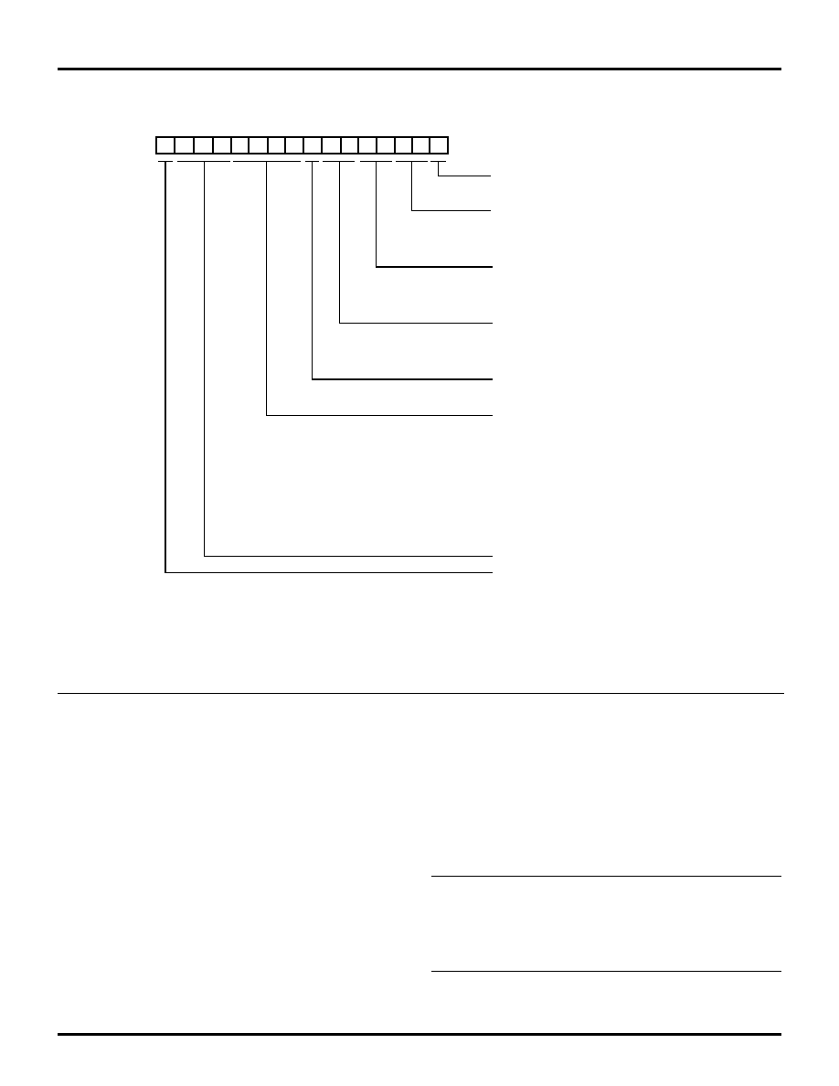
Z89223/273/323/373
ZiLOG
16-Bit Digital Signal Processors with A/D Converter
DS000202-DSP0599
41
C/T Registers
Each C/T contains a set of five 16-bit Registers. Bank13 is
used to access the registers for C/T0 and Bank14 is for the
C/T1 registers. All accesses to C/T Registers occur with
zero wait states.
Counter/Timer Control Register (Bank13,14/EXT1).
The
C/T Control register enables/disables the C/T, selects input
and output options, and the mode of operation.
TMLR--Load Register (Bank13,14/EXT2).
T h e 1 6 - b i t
TMLR register holds the value that is loaded into TMR
when TMR underflows.
TMR--Counter Register (Bank13,14/EXT3).
TMR is a
16-bit down counter that holds the current C/T value. It can
be read like any other ordinary register. However, writing
to TMR is different than writing to an ordinary register. A
write to TMR causes the contents of TMLR to be written
into TMR, causing the C/T to be retriggered.
TPLR--Prescaler Load Register (Bank13,14/EXT4).
T h e
16-bit TPLR register holds the prescaler load value in its
lower 8 bits. Bit 15 must be written with a "1", and bits 14≠8
must be written with "0's".
Note: If the C/T interrupt is being used, this register must be re-
written at the end of the interrupt service routine in order
to enable the next interrupt. The number of clock cycles
from the beginning of the interrupt service routine to the
write must exceed the prescaler load value.
Figure 32. C/T0 and C/T1 Control Register
D7
D6
D5
D4
D3
D2
D1
D0
D15 D14 D13 D12 D11 D10 D9
D8
Bank 13/EXT1 (C/T0) and Bank14/EXT1 (C/T1)
Input Event
00 = Falling Edge (default)
01 = Rising Edge
10 = Both Rising and Falling Edges
11 = Reserved
Output Select
00 = Outputs Unaffected (default)
01 = Reserved
10 = Drive TMO0 Pin
11 = Reserved
Output Polarity
0 = Output asserted High on Timeout (default)
1 = Output asserted Low on Timeout
Mode of Operation
0000 = Square Wave Output (default)
0001 = Retriggerable One-Shot
0010 = PWM (8-bit)
0011 = PWM (16-bit)
0100 = Finite Pulse String Generator
0101 = Externally-Clocked One-Shot
0110 = Software Watch-Dog Timer
0111 = Hardware Watch-Dog Timer
1000 = Pulse Stopwatch
1001 = Edge-to-edge Stopwatch
1010 = Edge Counter
1011 = Gated Edge Counter
Test Mode*
0 = Normal Operation
1 = Factory Test Mode
Reserved
C/T
0 = Disabled (default)
1 = Enabled
Input Select
00 = Inputs have no effect (default)
01 = Reserved
10 = UI0 Pin
11 = UI1 Pin
*Note: The user should always program this bit to "0".
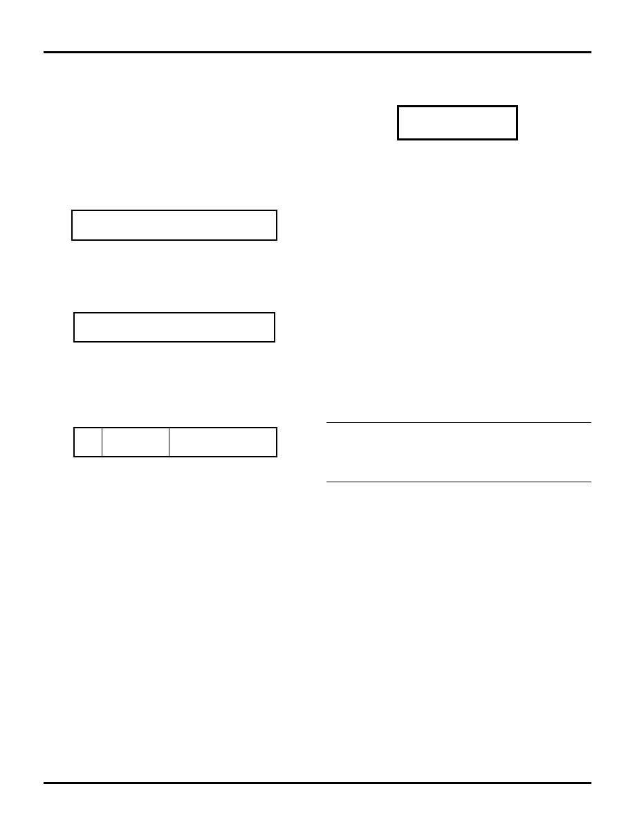
Z89223/273/323/373
16-Bit Digital Signal Processors with A/D Converter
ZiLOG
42
DS000202-DSP0599
PERIPHERALS (Continued)
TPR--Prescaler Register (Bank13,14/EXT5).
TPR is an
8-bit down counter that holds the current Prescaler Count
Value. It can be read like any other ordinary register. How-
ever, writing to TPR is different than writing to an ordinary
register. A write to TPR causes the lower 8-bit contents of
TPLR to be written into TPR, causing the Prescaler to be
retriggered.
Prescaler Operation
The Prescaler section comprises TPLR and TPR, followed
by a divide-by-two flip-flop. This operation generates a 50
percent duty cycle output, TMCLKIN. TPR's input clock
is the system clock. The maximum prescaler output fre-
quency is 1/2 the system clock frequency.
After TPR is loaded, it decrements at the system clock fre-
quency and generates an output to the divide-by-two flip-
flop. When the count reaches 0, the TPR counter is reloaded
from the lower 8 bits of TPLR Register.
Two other events cause a reloading of the TPR counter:
1. Writing to TPR
2. Reloading TMR, which happens when TMR under-
flows, or when TMR is written.
Note: For C/T Modes 8≠11, the external input signal on UI0 or
UI1 is synchronized with TMCLKIN before being ap-
plied to TMR. The external input signal frequency must
be no higher than 1/2 of the TMCLKIN frequency.
Figure 33. TMLR--Load Register
Figure 34. TMR--Counter Register
Figure 35. TPLR--Prescaler Load Register
Timer Reload Value
Bank 13,14/EXT2
15
0
Timer Register
Bank 13,14/EXT3
15
0
Prescaler
Reload Value
14
8 7
Zeros
15
0
“1”
Bank 13,14/EXT4
Figure 36. TPR--Prescaler Register
7
TPR
8-Bit Counter
0
Bank 13,14/EXT5
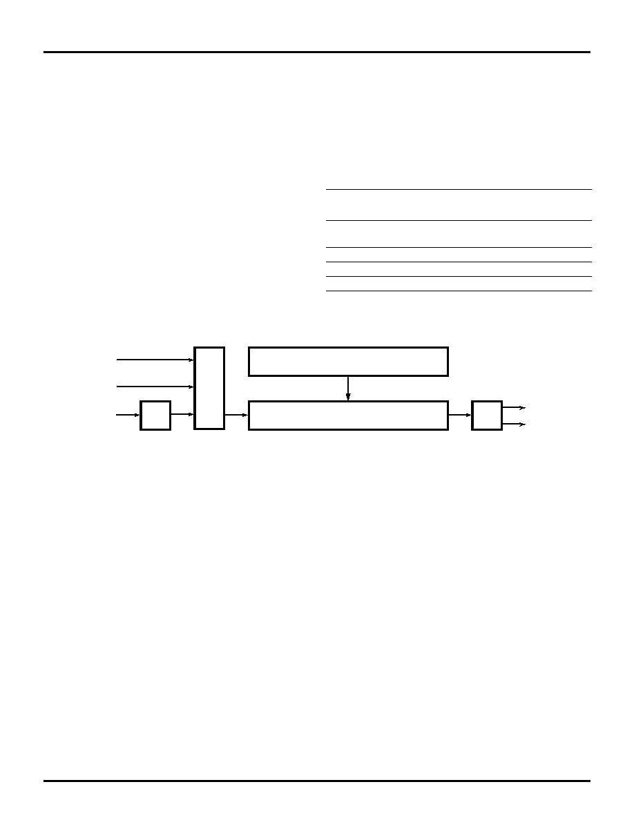
Z89223/273/323/373
ZiLOG
16-Bit Digital Signal Processors with A/D Converter
DS000202-DSP0599
43
GENERAL-PURPOSE COUNTER/TIMER (C/T2)
This versatile16-bit C/T offers multiple uses, including
Sleep Mode Wake-up. It can be clocked with the slow
32 kHz crystal clock (CLKI), while the DSP and other pe-
ripheral functions operate at a higher frequency generated
by the PLL. Also included is an independent long duration
timer.
GPT is a 16-bit down counter that holds the current C/T val-
ue. It can be read like any other ordinary register. GPTL and
GPT share the same address, Bank14/EXT0. A write to
GPTL reloads GPT, causing the C/T to be retriggered.
When C/T2 underflows, it is reloaded with the most recent
value written to GPTL. If the C/T2 interrupt is enabled, at
underflow an interrupt is generated. The counting operation
of the counter can be disabled. The C/T clock source can
be selected to be CLKI, UI2, or the system clock divided
by 2. When the C/T2 output is enabled, it drives the TMO2
pin.
Bank 15/EXT2 is the control register for C/T2, and for I/O
Ports 2 and 3. Refer to the I/O Ports section, page 33, for a
description of the I/O port bit allocation.
Table 22. C/T2 Bits D15 and D13
D15
D13
C/T2 Clock
Sleep/Wake-Up
Mode
0
0
SYSCLK ˜ 2
(default)
n/a
0
1
UI2
n/a
1
0
CLKI
Disabled
1
1
CLKI
Enabled
Figure 37. Counter/Timer2 Block Diagram
15
0
TMR
TMO2
Sleep Mode
Wake-Up
Timer Load Register
16-Bit Down Counter
GPT≠Bank14/EXT0 (Read)
GPTL≠Bank14/EXT0 Write
15
0
System Clock
UI2
CLKI
MUX
˜
2
MUX
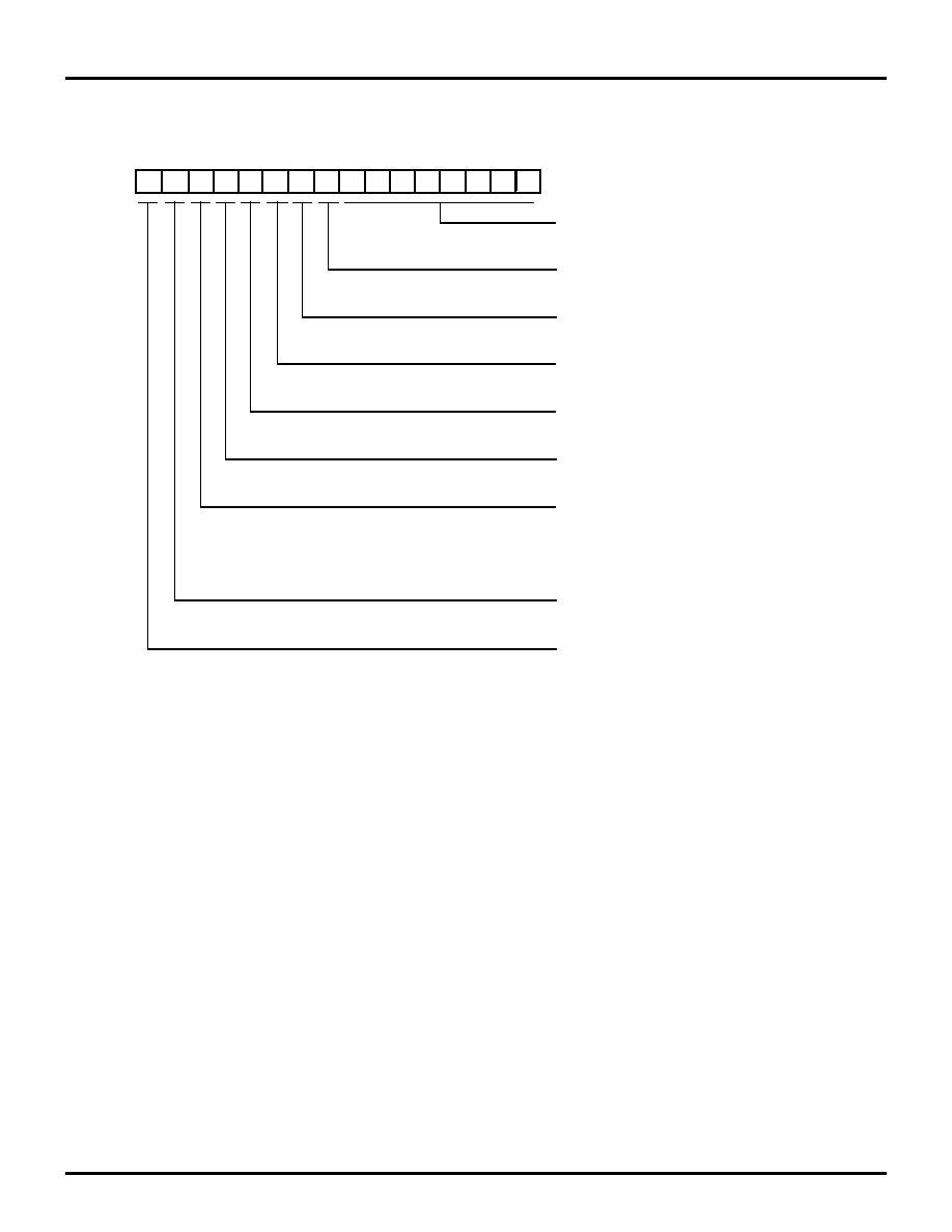
Z89223/273/323/373
16-Bit Digital Signal Processors with A/D Converter
ZiLOG
44
DS000202-DSP0599
GENERAL-PURPOSE COUNTER/TIMER (C/T2) (Continued)
Figure 38. Counter/Timer2 Control Register
D7 D6
D5 D4 D3
D2 D1 D0
D15 D14 D13 D12 D11 D10 D9
D8
Bank 15/EXT2
Port2 I/O Directions
0 = Input (default)
1 = Output
Port3
0 = Disabled (default)
1 = Enabled
INT0
0 = Disabled (default)
1 = Enabled
Port2 Outputs
0 = Push-Pull (default)
1 = Open-Drain
Counter/Timer2
0 = Disabled (default)
1 = Enabled
Counter/Timer2 Operation
0 = Stopped (default)
1 = Counting
If D15 = 0, Counter/Timer2 Clock defined by
0 = System Clock/2 (default)
1 = UI2
If D15 = 1, Counter/Timer2 Sleep Mode Wake-Up
0 = Disabled (default)
1 = Enabled
TMO2
Counter/Timer2 Clock
0 = Disabled (default)
1 = Enabled
0 = Defined by D13 (default)
1 = CLKI
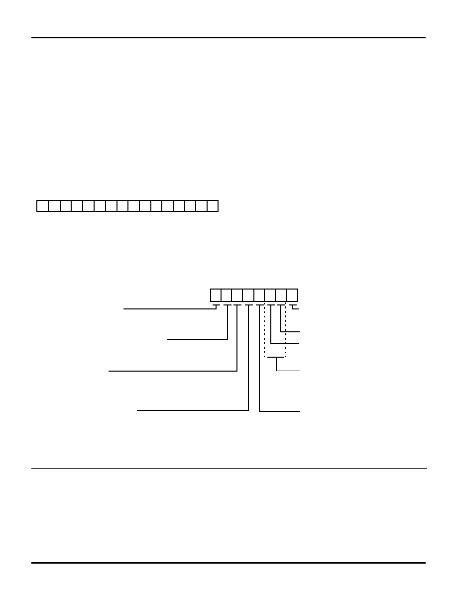
Z89223/273/323/373
ZiLOG
16-Bit Digital Signal Processors with A/D Converter
DS000202-DSP0599
45
SERIAL PERIPHERAL INTERFACE
The Z893x3 incorporates a Serial Peripheral Interface (SPI)
for communication with other microcontrollers and periph-
erals. The SPI can be operated either as the system Master,
or as a system Slave. The SPI consists of three registers: the
SPI Control Register (Bank15/EXT4), the SPI Re-
ceive/Buffer Register (RxBUF), and the SPI Shift Register.
SPI Data Access
Receive operations are double buffered. Bank0/EXT3 ac-
cesses both RxBUF for read (receive) operations, and the
SPI shift register for write (transmit) operations.
SPI Control Register
This register is the Low byte of Bank15/EXT4. It is a
read/write register that controls Master/Slave selection, SS
polarity, clock source and phase selection, and indicates
byte available and data overrun conditions. The control reg-
ister is multifunction depending on Master/Slave mode se-
lection.
In Master mode, Bit 6 defines the SPI clock source. A "1"
selects SCLK = C/T0 output, and a "0" selects SCLK = Sys-
tem Clock divided down by 2, 4, 8, or 16, as determined by
bits 1 and 2.
In Slave Mode, bit 1 is the Receive Byte Overrun flag. This
flag can be cleared by writing a "0" to this bit. Bit 2 is the
SDO output enable.A "0" tristates SDO, a "1" enables data
output on SDO. Bit 4 signals that a receive byte is available
in the RxBUF Register. If the associated interrupt enable
bit is enabled, an interrupt is generated.
Master Mode Operation
The DSP must first activate the target slave's select pin
through an I/O port. Loading data into the SPI Shift Register
initiates the transfer. Data is transferred out the SDO pin to
the slave one data bit per SCLK cycle. The MSB is shifted
out first. At the conclusion of the transfer, the Receive Byte
Available flag is set, and if enabled, an SPI interrupt is gen-
erated. The Receive Byte Available flag is reset when Rx-
BUF is read.
Figure 39. SPI Data Access
D15 D14
Bank 0/EXT 3 Register
D7 D6
D5 D4
D3
D2
D1
D0
Bits 7–0 SPI Data (SPI Shift Register for transmit and RxBUF for receive)
Bit 14 Receive Character Available
Bit 15 Receive Character Overrun
Figure 40. SPI Control Register
D7 D6 D5 D4 D3 D2 D1 D0
SPI Enable
0 = Disable (default)
1 = Enable
Bank15/EXT4 (LSB)
Receive Byte Overrun (Slave)
Output Enable(Slave)
0 = Tri-State SDO
1 = Enable SDO as Output
Slave Select Polarity
0 = SS Active Low (default)
1 = SS Active High
Received Byte Available
SCLK Polarity
0 = Transmit on Falling Edge, Receive on Rising Edge
1 = Transmit on Rising Edge, Receive on Falling Edge
SPI Clock Source Select (Master)
0 = System Clock divided down.
1 = C/T0
Mode of Operation
1 = Master
SCLK Frequency (Master)
00 = System Clock
˜
2
01 = System Clock
˜
4
10 = System Clock
˜
8
11 = System Clock
˜
16
0 = Slave
Z89223/273/323/373
16-Bit Digital Signal Processors with A/D Converter
ZiLOG
46
DS000202-DSP0599
SERIAL PERIPHERAL INTERFACE (Continued)
Slave Mode Operation
SS must be asserted to enable a data transfer. Incoming data
on the SDI pin is shifted into the SPI Shift Register one data
bit per SCLK cycle. When a byte of data is received, the
SPI Shift Register contents are automatically copied into
RxBUF. The Receive Byte Available flag is set, and if en-
abled, an SPI interrupt is generated. The next byte of data
may be received at this time. The current byte in RxBUF
must be read before the next byte's reception is complete,
or the Receive Byte Overrun flag will set, and the data in
RxBUF will be overwritten. The Receive Byte Available
flag is reset when RxBUF is read.
Unless the SPI output, SDO, is disabled, for every bit that
is transferred into the slave through the SDI pin, a bit is
transferred out through the SDO pin on the opposite clock
edge. During slave operation, SCLK is an input.
Note: Slave Mode is not available on the 44-pin package.
Figure 41. SPI Block Diagram
SPI Clock
SPI
Counter
Interrupt
SPI∑
I/O
SPI Shift Register
SPI Receive Buffer (RxBuf)
SPI Control (SCON)
INT
SCLK/P1.5
SDO/P1.3
SDI/P1.2
SS/P1.4
C/T0
System
Clock
(from PLL Block)
Z89223/273/323/373
ZiLOG
16-Bit Digital Signal Processors with A/D Converter
DS000202-DSP0599
47
SYSTEM CLOCK GENERATOR
The System Clock can be generated from an external clock
signal, or from the internal crystal oscillator. For the latter
case, a 32-kHz crystal is used in conjunction with the in-
ternal crystal oscillator. The system clock generator in-
cludes a Phase-Locked Loop (PLL) circuit to derive a high-
frequency System Clock from the low-frequency crystal os-
cillator. The benefits of using a low-frequency crystal are
lower system cost, lower power consumption and lower
EMI.
The Z893x3 supports several low-power clock modes to op-
timize power consumption. Total power consumption de-
pends on System Clock frequency, and which oscillators
and peripherals are enabled.
Modes of Operation
The various modes of clock operation are selected by writ-
ing to the appropriate bits and fields of the Clock Control
Register, Bank15/EXT5. The mode of operation can be
switched dynamically during program execution.
Power-up and Reset (Default)
At power-up, and following a reset or Sleep Mode Recov-
ery, System Clock Select = 0, therefore system clock =
CLKI. The XTAL Oscillator is running, so CLKI may be
provided by a crystal, as depicted, or by an external clock
(not shown). The VCO is running to minimize the time re-
quired to switch the system clock to PLL Out.
External Clock Direct
In this mode, an external clock on CLKI provides the Sys-
tem Clock. CLKO is not connected. System Clock Select
= 0. The PLL is not used. The XTAL oscillator and VCO
are both stopped to reduce power consumption.
Crystal Oscillator DIrect
In this mode of operation, the XTAL Oscillator is running,
and an external crystal provides a 32-kHz (typical) clock
at CLKI. System Clock Select = 0, so the System Clock is
the frequency at CLKI (32 kHz). This mode requires less
power than running at a high-frequency clock rate. The
VCO may be stopped to conserve even more power, or left
running for rapid switching (wake up) to a high-frequency
PLL generated clock. Whenever the PLL circuit is enabled,
Stop VCO = 0, and a software delay of 10 ms must be ob-
served before switching System Clock from CLKI to PLL
Out. As a result, the PLL has time to stabilize.
PLL Clock
An external 32-kHz crystal, together with the on-chip
XTAL oscillator, provides the PLL input. The VCO gen-
erates the System Clock. A low-pass filter must be connect-
ed to LPF as depicted. The XTAL oscillator and VCO are
both running, and System Clock = PLL Out (System Clock
Select = 1). The frequency generated by the PLL is deter-
Figure 42. System Clock Generator
VCO
8-Bit
Phase
Detector
Stop VCO
PLL Out. Sel.
PLL Divisor
System
Stop XTAL Osc
LPF
32 kHz
On-Chip
Off-Chip
System Clock
00
Clock
Divide
LPF
CLKI
CLKO
Clock
Control
Register
MUX
MUX
˜
2
˜
2
˜
2
01
10
11
0
1
XTAL
Osc.
PLL Out
Clock
Select
PLL
VCO Out
PLL In
CLKI
Z89223/273/323/373
16-Bit Digital Signal Processors with A/D Converter
ZiLOG
48
DS000202-DSP0599
SYSTEM CLOCK GENERATOR (Continued)
mined by the PLL Divisor value in the MSB of the Clock
Control Register, Bank15/EXT5:
VCO Frequency = 4 x PLL Divisor x PLL In Frequency.
The PLL Divisor value should be between 1 and156 to ob-
tain a VCO Frequency between 128 kHz and 20 MHz from
a 32-kHz input.
There are four options for PLL Out: VCO Out, VCO Out
divided by 2, VCO Out divided by four, or twice the crystal
frequency. This selection is determined by the PLL Out Se-
lect bits in the Clock Control Register.
Note: The PLL is designed and tested to operate with an input
frequency of approximately 32 kHz. It is possible to
drive the input with a crystal or user-generated clock at
some other frequency, but the results are not guaranteed.
Sleep Modes
The Z893x3 supports various Clock Modes to minimize de-
vice power consumption. The lowest power mode is Deep
Sleep in which the System Clock is stopped, and the VCO
and XTAL Oscillator are both turned off.
Wake-Up From Sleep Modes
The Wake-up Trigger Source is specified by bits 5 and 6
of the Clock Control Register. The polarity of the Wake-
up signal is defined by bit 7. Wake-up occurs when the
wake-up signal is toggled to the specified wake-up polarity.
Wake-up resumes operation starting from the reset vector
address in the same way the chip responds to an external
RESET.
Table 23. Standard Clock Mode Summary
Mode
CLKI
Src
Stop
XTAL
Osc.
Stop
VCO
Sys
Clk
Sel
Power-up/Reset
(default)
XTAL,
User
0
0
0
PLL Clock
XTAL
0
0
1
Crystal Oscillator
Direct
XTAL
0
1
0
External Clock Direct
User
1
1
0
Deep Sleep
(lowest power)
XTAL,
User
1
1
1
Figure 43. System Clock Control Register
D7
D6
D5
D4
D3
D2 D1
D0
D15 D14 D13 D12 D11 D10 D9
D8
Bank 15/Ext 5 Reg
STOP Recovery Level
0 : Low (Default setting after reset)
1 : High
STOP_VCO
0 : VCO Running
1 : Stop VCO
BYPASS_PLL
0 : Clock Source is Oscillator
1 : Clock Source is VCO
DSP (System) Clock Source
00 : VCO Clock
01 : VCO Clock Divided by 2
10 : VCO Clock Divided by 4
11 : Twice the Crystal Frequency
Recovery Source
00 : POR (Power-On Reset) or
Port 2, Bit 0 (INT0)
01 : POR or Port 1, Bit 4 (SS)
10 : POR or Port 1, Bit 6 (UI0)
11 : POR or Port 2, Bit 0 or
Port 1, Bit 4 or Port 1, Bit 6
Programmable PLL Divider Register
System Clock = Bits 15–8 x 4 x Crystal Frequency (32.768 kHz)
STOP_OSC
0 : Oscillator Running
1 : Stop Oscillator

Z89223/273/323/373
ZiLOG
16-Bit Digital Signal Processors with A/D Converter
DS000202-DSP0599
49
INSTRUCTION SET
The addressing modes are:
<pregs>, <hwregs>.
These modes are used for loads to
and from registers within the chip, such as loading to the
accumulator, or loading from a pointer register. The names
of the registers are specified in the operand field (destination
first, then source).
<dregs>.
This mode is used for access to the lower 16 ad-
dresses in each bank of RAM. The 4-bit address comes from
2 bits of the status register and 2 bits of the operand field
of the data pointer. Data registers can be used to access data
in RAM, but typically are used as pointers to access data
from the program memory.
<accind>.
Similar to the previous mode, the address for the
program memory read is stored in the Accumulator. Hence,
@A in the second operand field loads the number in mem-
ory specified by the address in A.
<direct>.
The direct mode allows read or write to data RAM
from the Accumulator by specifying the absolute address
of the RAM in the operand of the instruction. A number be-
tween 0 and 255 indicates a location in RAM bank 0, and
a number between 256 and 511 indicates a location in RAM
bank 1.
<limm>.
This address mode indicates a long immediate op-
erand. A 16-bit word can be loaded directly from the oper-
and into the specified register or memory location.
<simm>.
This address mode indicates a short immediate
operand. It is used to load 8-bit data into the specified RAM
pointer.
<regind>.
This mode is used for indirect access to the data
RAM. The address of the RAM location is stored in the
pointer. The "@" symbol indicates "indirect" and precedes
the pointer. For example, @P1:1 refers to the location in
RAM bank 1 specified by the value in the pointer.
<memind>.
This mode is used for indirect access to the
program memory. The address of the memory is located in
a RAM location, which is specified by the value in a pointer.
Therefore, @@P1:1 instructs the processor to read from a
location in memory, which is specified by a value in RAM,
and the location of the RAM is in turn specified by the value
in the pointer.
Note: the data pointer can also be used for a memory access in
this manner, but only one "@" precedes the pointer. In
both cases, each time the addressing mode is used, the
memory address stored in RAM is incremented by one
to allow easy transfer of sequential data from program
memory.
Table 24. Instruction Set Addressing Modes
Symbolic Name
Syntax
Description
<pregs>
Pn:b
Pointer Registers
<dregs> (points to RAM)
Dn:b
Data Registers
<hwregs>
X, Y, PC, SR, P, EDn, A, BUS Hardware Registers
<accind> (points to Program
Memory)
@A
Accumulator Memory Indirect
<direct>
<expression>
Direct Address Expression
<limm>
#<const exp>
Long (16-bit) Immediate Value
<simm>
#<const exp>
Short (8-bit) Immediate Value
<regind> (points to RAM)
@Pn:b
Pointer Register Indirect
@Pn:b+
Pointer Register Indirect with Increment
@Pn:b≠LOOP
Pointer Register Indirect with Loop
Decrement
@Pn:b+LOOP
Pointer register Indirect with Loop Increment
<memind> (points to Program
Memory)
@@Pn:b
Pointer Register Memory Indirect
@Dn:b
Data Register Memory Indirect
@@Pn:b≠LOOP
Pointer Register Memory Indirect with Loop
Decrement
@@Pn:b+LOOP
Pointer Register Memory Indirect with Loop
Increment
@@Pn:b+
Pointer Register Memory Indirect with
Increment

Z89223/273/323/373
16-Bit Digital Signal Processors with A/D Converter
ZiLOG
50
DS000202-DSP0599
CONDITION CODES
The following Instruction Description defines the condition
codes supported by the DSP assembler. If the instruction
description refers to the <cc> (condition code) symbol in
one of its addressing modes, the instruction only executes
if the condition is true.
Code
Description
C
Carry
EQ
Equal (same as Z)
F
False
IE
Interrupts Enabled
MI
Minus
NC
No Carry
NE
Not Equal (same as NZ)
NIE
Not Interrupts Enabled
NOV
Not Overflow
NU0
Not User Zero
NU1
Not User One
NZ
Not zero
OV
Overflow
PL
Plus (Positive)
U0
User Zero
U1
User One
UGE
Unsigned Greater Than or Equal (Same as
NC)
ULT
Unsigned Less Than (Same as C)
Z
Zero

Z89223/273/323/373
ZiLOG
16-Bit Digital Signal Processors with A/D Converter
DS000202-DSP0599
51
INSTRUCTION DESCRIPTIONS
Inst.
Description
Synopsis
Operands
Words
Cycles Examples
ABS
Absolute
Value
ABS[<cc>,]<src>
<cc>,A
A
1
1
1
1
ABS NC, A
ABS A
ADD
Addition
ADD<dest>,<src>
A,<pregs>
A,<dregs>
A,<limm>
A,<memind>
A,<direct>
A,<regind>
A,<hwregs>
A,<simm>
1
1
2
1
1
1
1
1
1
1
2
3
1
1
1
1
ADD A,P0:0
ADD A,D0:0
ADD A,#%1234
ADD A,@@P0:0
ADD A,%F2
ADD A,@P1:1
ADD A,X
ADD A, #%12
AND
Bitwise AND AND<dest>,<src>
A,<pregs>
A,<dregs>
A,<limm>
A,<memind>
A,<direct>
A,<regind>
A,<hwregs>
A,<simm>
1
1
2
1
1
1
1
1
1
1
2
3
1
1
1
1
AND A,P2:0
AND A,D0:1
AND A,#%1234
AND A,@@P1:0
AND A,%2C
AND A,@P1:2+LOOP
AND A,EXT3
AND A, #%12
CALL
Subroutine
call
CALL
[<cc>,]<address>
<cc>,<direct>
<direct>
2
2
2
2
CALL Z,sub2
CALL sub1
CCF
Clear C flag
CCF
None
1
1
CCF
CIEF
Clear IE Flag
CIEF
None
1
1
CIEF
COPF
Clear OP flag COPF
None
1
1
COPF
CP Comparison
CP<src1>,<src2>
A,<pregs>
A,<dregs>
A,<memind>
A,<direct>
A,<regind>
A,<hwregs>
A,<limm>
A,<simm>
1
1
1
1
1
1
2
1
1
1
3
1
1
1
2
1
CP A,P0:0
CP A,D3:1
CP A,@@P0:1
CP A,%FF
CP A,@P2:1+
CP A,STACK
CP A,#%FFCF
CP A, #%12
DEC
Decrement
DEC [<cc>,]<dest>
<cc>A,
A
1
1
1
1
DEC NZ,A
DEC A
INC
Increment
INC [<cc>,] <dest>
<cc>,A
A
1
1
1
1
INC PL,A
INC A
JP
Jump
JP [<cc>,]<address> <cc>,<direct>
<direct>
2
2
2
2
JP C,Label
JP Label

Z89223/273/323/373
16-Bit Digital Signal Processors with A/D Converter
ZiLOG
52
DS000202-DSP0599
INSTRUCTION DESCRIPTIONS (Continued)
LD
Load
destination
with source
LD<dest>,<src>
A,<hwregs>
A,<dregs>
A,<pregs>
A,<regind>
A,<memind>
A,<direct>
<direct>,A
<dregs>,<hwregs>
<pregs>,<simm>
<pregs>,<hwregs>
<regind>,<limm>
<regind>,<hwregs>
<hwregs>,<pregs>
<hwregs>,<dregs>
<hwregs>,<limm>
<hwregs>,<accind>
<hwregs>,<memind>
<hwregs>,<regind>
<hwregs>,<hwregs>
1
1
1
1
1
1
1
1
1
1
1
1
1
1
2
1
1
1
1
1
1
1
1
3
1
1
1
1
1
1
1
1
1
2
3
3
1
1
LD A,X
LD A,D0:0
LD A,P0:1
LD A,@P1:1
LD A,@D0:0
LD A,124
LD 124,A
LD D0:0,EXT7
LD P1:1,#%FA
LD P1:1,EXT1
LD@P1:1,#1234
LD @P1:1+,X
LD Y,P0:0
LD SR,D0:0
LD PC,#%1234
LD X,@A
LD Y,@D0:0
LD A,@P0:0≠LOOP
LD X,EXT6
Notes:
When <dest> is <hwregs>, <dest> cannot be P.
When <dest> is <hwregs> and <src> is <hwregs>, <dest> cannot be EXTn if <src> is EXTn,
<dest> cannot be X if <src> is X, <dest> cannot be SR if <src> is SR.
When <src> is <accind> <dest> cannot be A.
MLD
Multiply
MLD <src1>,<src2>
[,<bank switch>]
<hwregs>,<regind>
<hwregs>,<regind>,
<bank switch>
<regind>,<regind>
<regind>,<regind>,
<bank switch>
1
1
1
1
1
1
1
1
MLD A,@P0:0+LOOP
MLD A,@P1:0,OFF
MLD @P1:1,@P2:0
MLD @P0:1,@P1:0,ON
Notes:
If src1 is <regind> it must be a bank 1 register. Src2's <regind must be a bank 0 register.
<hwregs> for src1 cannot be X.
For the operands <hwregs>, <regind> the <bank switch> defaults to OFF. For the operands
<regind>, the <bank switch> defaults to ON.
MPYA
Multiply and
add
MPYA <src1>,<src2>
[,<bank switch>]
<hwregs>,<regind>
<hwregs>,<regind>,
<bank switch>
<regind>,<regind>
<regind>,<regind>,
<bank switch>
1
1
1
1
1
1
1
1
MPYA A,@P0:0
MPYA A,@P1:0,OFF
MPYA @P1:1,@P2:0
MPYA@P0:1,@P1:0,ON
Notes:
If src1 is <regind> it must be a bank 1 register. Src2's <regind> must be a bank 0 register.
<hwregs> for src1 cannot be X.
For the operands <hwregs>, <regind> the <bank switch> defaults to OFF. For the operands <regind>, the <bank
switch> defaults to ON.
MPYS
Multiply and
subtract
MPYS <src1>,<src2>
[,<bank switch>]
<hwregs>,<regind>
<hwregs>,<regind>,
<bank switch>
<regind>,<regind>
<regind>,<regind>,
<bank switch>
1
1
1
1
1
1
1
1
MPYS A,@P0:0
MPYS A,@P1:0,OFF
MPYS @P1:1,@P2:0
MPYS
@P0:1,@P1:0,ON
Inst.
Description
Synopsis
Operands
Words
Cycles Examples

Z89223/273/323/373
ZiLOG
16-Bit Digital Signal Processors with A/D Converter
DS000202-DSP0599
53
Notes:
If src1 is <regind> it must be a bank 1 register. Src2's <regind> must be a bank 0 register.
<hwregs> for src1 cannot be X.
For the operands <hwregs>, <regind> the <bank switch> defaults to OFF. For the operands <regind>, <regind>
the <bank switch> defaults to ON.
NEG
Negate
NEG <cc>,A
<cc>, A
A
1
1
1
1
NEG MI,A
NEG A
NOP
No operation NOP
None
1
1
NOP
OR
Bitwise OR
OR <dest>,<src>
A,<pregs>
A,<dregs>
A,<limm>
A,<memind>
A,<direct>
A,<regind>
A,<hwregs>
A,<simm>
1
1
2
1
1
1
1
1
1
1
2
3
1
1
1
1
OR A,P0:1
OR A, D0:1
OR A,#%2C21
OR A,@@P2:1+
OR A, %2C
OR A,@P1:0≠LOOP
OR A,EXT6
OR A,#%12
POP
Pop value
from stack
POP <dest>
<pregs>
<dregs>
<regind>
<hwregs>
1
1
1
1
1
1
1
1
POP P0:0
POP D0:1
POP @P0:0
POP A
PUSH
Push value
onto stack
PUSH <src>
<pregs>
<dregs>
<regind>
<hwregs>
<limm>
<accind>
<memind>
1
1
1
1
2
1
1
1
1
1
1
2
3
3
PUSH P0:0
PUSH D0:1
PUSH @P0:0
PUSH BUS
PUSH #12345
PUSH @A
PUSH @@P0:0
RET
Return from
subroutine
RET
None
1
2
RET
RL
Rotate Left
RL <cc>,A
<cc>,A
A
1
1
1
1
RL NZ,A
RL A
RR
Rotate Right
RR <cc>,A
<cc>,A
A
1
1
1
1
RR C,A
RR A
SCF
Set C flag
SCF
None
1
1
SCF
SIEF
Set IE flag
SIEF
None
1
1
SIEF
SLL Shift
left
logical
SLL [<cc>,]A
A
1
1
1
1
SLL NZ,A
SLL A
SOPF
Set OP flag
SOPF
None
1
1
SOPF
SRA
Shift right
arithmetic
SRA<cc>,A
<cc>,A
A
1
1
1
1
SRA NZ,A
SRA A
SUB
Subtract
SUB<dest>,<src>
A,<pregs>
A,<dregs>
A,<limm>
A,<memind>
A,<direct>
A,<regind>
A,<hwregs>
A,<simm>
1
1
2
1
1
1
1
1
1
1
2
3
1
1
1
1
SUB A,P1:1
SUB A,D0:1
SUB A,#%2C2C
SUB A,@D0:1
SUB A,%15
SUB A,@P2:0≠LOOP
SUB A,STACK
SUB A, #%12
Inst.
Description
Synopsis
Operands
Words
Cycles Examples

Z89223/273/323/373
16-Bit Digital Signal Processors with A/D Converter
ZiLOG
54
DS000202-DSP0599
INSTRUCTION DESCRIPTIONS (Continued)
Bank Switch Operand.
The third (optional) operand of
the MLD, MPYA and MPYS instructions represents wheth-
er the bank switch is set to ON or OFF. To illustrate, the
keywords ON and OFF are used to state the direction of the
switch. These keywords are referenced in the instruction de-
scriptions through the <bank switch> symbol. The most no-
table capability is that a source operand can be multiplied
by itself (squared).
XOR
Bitwise
exclusive OR
XOR <dest>,<src>
A,<pregs>
A,<dregs>
A,<limm>
A,<memind>
A,<direct>
A,<regind>
A,<hwregs>
A,<simm>
1
1
2
1
1
1
1
1
1
1
2
3
1
1
1
1
XOR A,P2:0
XOR A,D0:1
XOR A,#13933
XOR A,@@P2:1+
XOR A,%2F
XOR A,@P2:0
XOR A,BUS
XOR A, #%12
Inst.
Description
Synopsis
Operands
Words
Cycles Examples
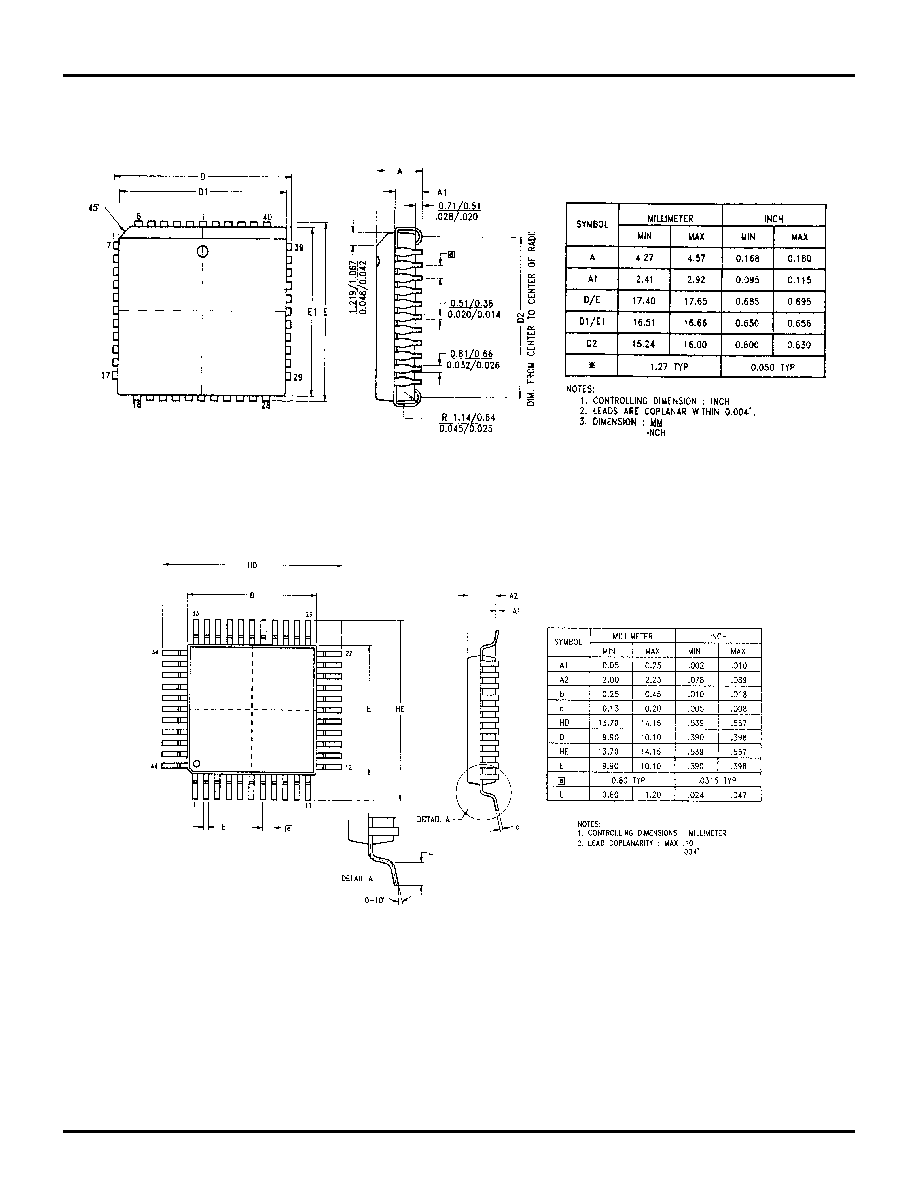
Z89223/273/323/373
ZiLOG
16-Bit Digital Signal Processors with A/D Converter
DS000202-DSP0599
55
PACKAGE INFORMATION
Figure 44. 44-Pin PLCC Package Diagram
Figure 45. 44-Pin PQFP Package Diagram
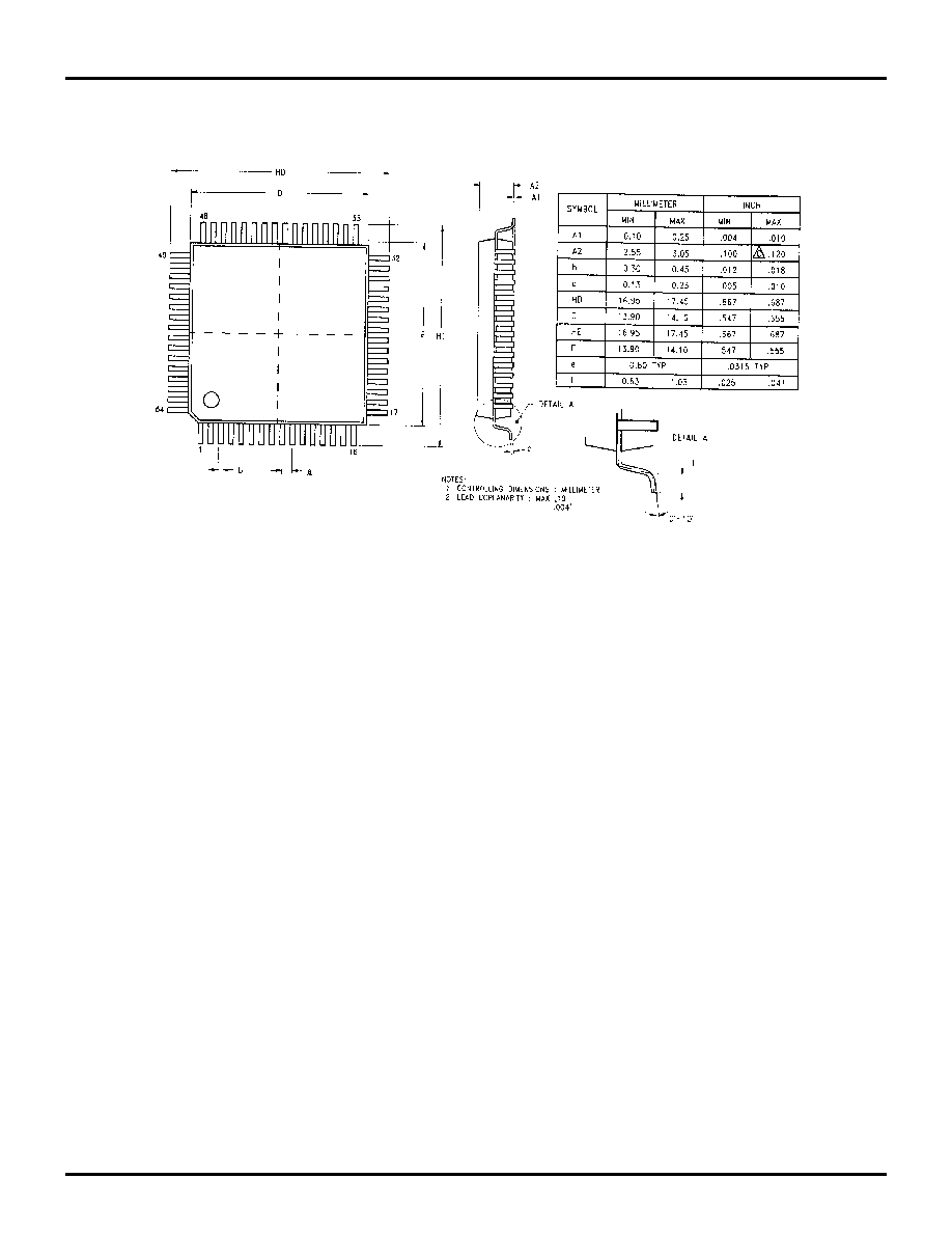
Z89223/273/323/373
16-Bit Digital Signal Processors with A/D Converter
ZiLOG
56
DS000202-DSP0599
PACKAGE INFORMATION (Continued)
Figure 46. 64-Pin TQFP Package Diagram
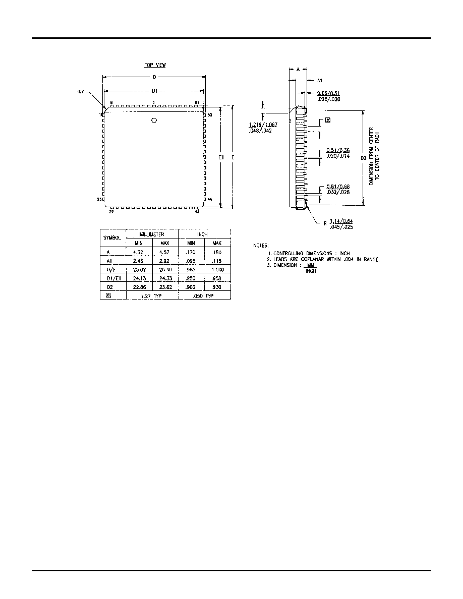
Z89223/273/323/373
ZiLOG
16-Bit Digital Signal Processors with A/D Converter
DS000202-DSP0599
57
Figure 47. 68-Pin PLCC Package Diagram
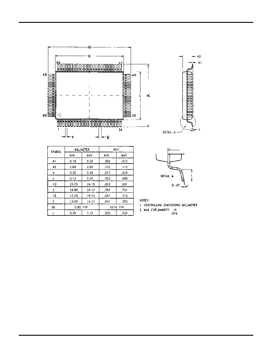
Z89223/273/323/373
16-Bit Digital Signal Processors with A/D Converter
ZiLOG
58
DS000202-DSP0599
PACKAGE INFORMATION (Continued)
Figure 48. 80-Pin PQFP Package Diagram
Z89223/273/323/373
ZiLOG
16-Bit Digital Signal Processors with A/D Converter
DS000202-DSP0599
59
ORDERING INFORMATION
For fast results, contact your local ZiLOG sales office for
assistance in ordering the part required.
CODES
Package Type
ROM
OTP
44-Pin PLCC
Z8922320VSC
Z8927320VSC
Z8922320VEC
44-Pin PQFP
Z8922320FSC
Z8922320FEC
64-Pin TQFP
Z8932320ASC
Z8937320ASC
Z8932320AEC
68-Pin PLCC
Z8932320VSC
Z8937320VSC
Z8932320VEC
80-Pin PQFP
Z8932320FSC
Z8937320FSC
Z8932320FEC
Package
V = PLCC
A = TQFP
F = PQFP
Temperature
S = 0∞C to +70∞C
E = ≠40∞C to 85∞C
Speed
20 = 20 MHz
Environmental
C = Plastic Standard
Example:
Z 89323 20 V S C
Environmental Flow
Temperature
Package
Speed/Bond Out Option
Product Number
ZiLOG Prefix
is a Z89323, 20 MHz, PLCC, 0∞C to +70∞C, Plastic Standard Flow

Z89223/273/323/373
16-Bit Digital Signal Processors with A/D Converter
ZiLOG
60
DS000202-DSP0599
©1999 by ZiLOG, Inc. All rights reserved. Information in this
publication concerning the devices, applications, or technology
described is intended to suggest possible uses and may be
superseded. ZiLOG, INC. DOES NOT ASSUME LIABILITY
FOR OR PROVIDE A REPRESENTATION OF ACCURACY
OF THE INFORMATION, DEVICES, OR TECHNOLOGY
DESCRIBED IN THIS DOCUMENT. ZiLOG ALSO DOES
NOT ASSUME LIABILITY FOR INTELLECTUAL
PROPERTY INFRINGEMENT RELATED IN ANY
MANNER TO USE OF INFORMATION, DEVICES, OR
TECHNOLOGY DESCRIBED HEREIN OR OTHERWISE.
Except with the express written approval of ZiLOG, use of
information, devices, or technology as critical components of
life support systems is not authorized. No licenses are conveyed,
implicitly or otherwise, by this document under any intellectual
property rights.
ZiLOG, Inc.
910 East Hamilton Avenue, Suite 110
Campbell, CA 95008
Telephone (408) 558-8500
FAX (408) 558-8300
Internet:
http://www.zilog.com