
DS97DSP0100
P R E L I M I N A R Y
1
1
P
RELIMINARY
P
RODUCT
S
PECIFICATION
Z89321/371/391
1
16-B
IT
D
IGITAL
S
IGNAL
P
ROCESSORS
FEATURES
s
0
∞
C to +70
∞
C Standard Temperature Range
-40
∞
C to +85
∞
C Extended Temperature Range
s
4.5- to 5.5-Volt Operating Range
DSP Core
s
24 MIPS @ 24 MHz Maximum, 16-Bit Fixed Point DSP
s
41.7 ns Minimum Instruction Cycle Time
s
Six-Level Hardware Stack
s
Six Register Address Pointers
s
Optimized Instruction Set (30 Instructions)
On-Board Peripherals
s
Dual 8/16-Bit CODEC Interface Capable of up to
10 Mbps
s
m
-Law Compression Option
(Decompression is Performed in Software)
s
16-Bit I/O Bus (Tri-Stated)
s
Three I/O Address Pins (Latched Outputs)
s
Wait-State Generator
s
Three Vectored Interrupts
s
13-Bit General-Purpose Timer
GENERAL DESCRIPTION
The Z893XX products are high-performance Digital Signal
Processors (DSPs) with a modified Harvard-type architec-
ture featuring separate program and data memory. The de-
sign has been optimized for processing power while mini-
mizing silicon space.
The single-cycle instruction execution and bus structure
promotes efficient algorithm execution, while the six regis-
ter pointers provide circular buffering capabilities and dual
operand fetching.
Three vectored interrupts are complemented by a six-level
stack, and the CODEC interface allows high-speed trans-
fer rates to accommodate digital audio and voice data.
A dedicated Counter/Timer provides the necessary timing
signals for the CODEC interface, and an additional 13-bit
timer is available for general-purpose use.
Device
DSP ROM
(KW)
OTP
(KW)
DSP RAM
Lines
MIPS
(Max)
Z89321
4
512
24
Z89371
4
512
16
Z89391
64*
512
24
Note:
*External
Device
40-Pin
DIP
44-Pin
PLCC
44-Pin
QFP
84-Pin
PLCC
Z89321
X
X
X
Z89371
X
X
X
Z89391
X
Note:
*General-Purpose
Z89321/371/391
16-Bit Digital Signal Processors
Zilog
2
P R E L I M I N A R Y
DS97DSP0100
The Z893XX DSPs are optimized to accommodate ad-
vanced signal processing algorithms. The 24 MIPS (maxi-
mum) operating performance and efficient architecture
provides real-time instruction execution. Compression, fil-
tering, frequency detection, audio, voice detection/synthe-
sis, and other vital algorithms can all be accommodated.
The Z89321/371/391 devices feature an on-board CO-
DEC interface, compatible with 8-bit PCM and 16-bit CO-
DECs for digital audio applications. Additionally, an on-
board wait-state generator is provided to accommodate
slow external peripherals.
For prototypes, as well as production purposes, the
Z89371 member of the DSP product family is a one-time
pro-grammable (OTP) device with a 16 MHz maximum op-
erating frequency.
Notes:
All signals with a preceding front slash, "/", are
active Low. For example, B//W (WORD is active Low);
/B/W (BYTE is active Low, only).
Power connections follow conventional descriptions be-
low:
Connection
Circuit
Device
Power
V
CC
V
DD
Ground
GND
V
SS
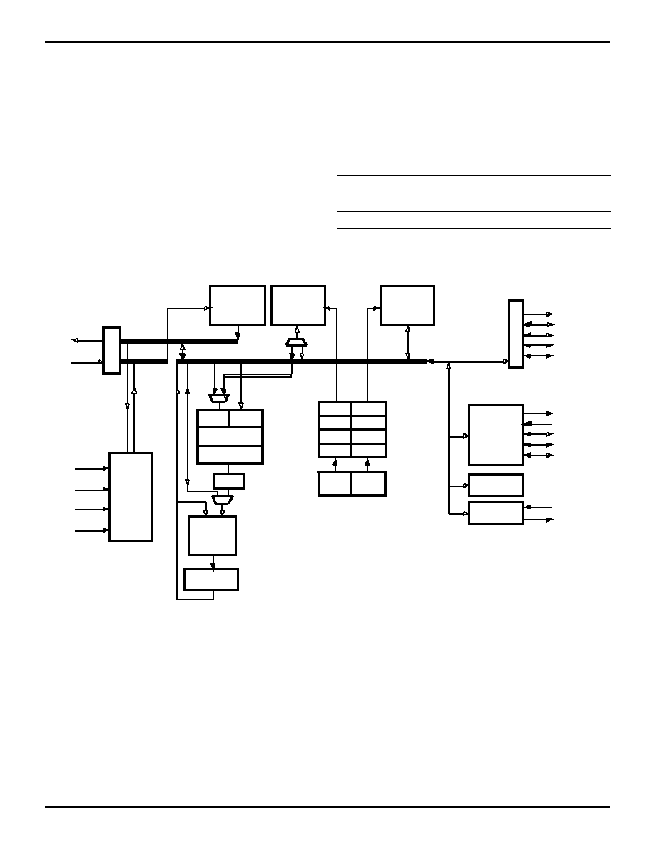
Figure 1. Z89321/371/391 Functional Block Diagram
Program
ROM/OTP
4096x16
Data RAM0
256x16
EA0-2
EXT0-15
/DS
WAIT
RD//WR
Data RAM1
256x16
DDATA
XDATA
PDATA
PADDR
PA0-15
PD0-15
Shifter
Arithmetic
Logic Unit
(ALU)
Program
Control
Unit
INT0-2
HALT
/RESET
CLK
Accumulator
8/16-Bit,
Full Duplex,
10 MBPS
Serial Port
TXD
RXD
SCLK
FS0
FS1
13-Bit Timer
User I/O
UI1-0
UO1-0
X
Y
Multiplier
P
DP0-3
DP4-6
P2
P2
P1
P1
P0
P0
ADDR
GEN0
ADDR
GEN1
Z89321/371/391
Zilog
16-Bit Digital Signal Processors
DS97DSP0100
P R E L I M I N A R Y
3
1
PIN DESCRIPTION
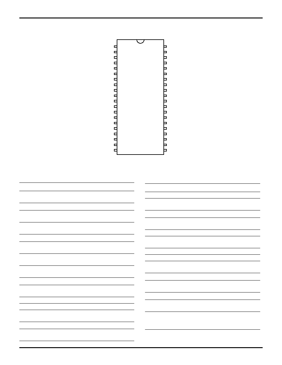
Figure 2. Z89321/371 40-Pin DIP Pin Assignments
EXT12
EXT13
EXT14
VSS
EXT15
EXT3
EXT4
VSS
EXT5
EXT6
EXT7
TXD
EXT8
EXT9
VSS
EXT10
EXT11
UI1
UI0
SCLK
RXD
VSS
EXT2
EXT1
EXT0
VSS
FS1
U01
U00
/INT0
FS0
CLK
/DS
VDD
EA2
EA1
EA0
/RESET
RD//WR
VDD
40
DIP 40 - Pin
1
20
21
Table 1. Z89321/371 40-Pin DIP Pin IdentiÞcation
No.
Symbol
Function
Direction
1-3
EXT12-
EXT14
External Data
Bus
Input/Output
4
V
SS
Ground
5
EXT15
External Data
Bus
Input/Output
6-7
EXT3-EXT4
External Data
Bus
Input/Output
8
V
SS
Ground
9-11
EXT5-EXT7
External Data
Bus
Input/Output
12
TXD
Serial Output to
CODECs
Output
13-14
EXT8-EXT9
External Data
Bus
Input/Output
15
V
SS
Ground
16-17
EXT10-
EXT11
External Data
Bus
Input/Output
18
UI1
User Input
Input
19
UI0
User Input
Input
20
SCLK
CODEC Serial
Clock
Input/Output*
21
V
DD
Power Supply
Input
22
RD//WR
Strobes for
External Bus
Output
23
/RESET
Reset
Input
24-26
EA0-EA2
External Address
Bus
Output
27
V
DD
Power Supply
Input
28
/DS
Data Strobe for
External Bus
Output
29
CLK
Clock
Input
30
FS0
CODEC 0 Frame
Sync
Input/Output*
31
/INT0
Interrrupt
Input
32-33
UO0-UO1
User Output
Output
34
FS1
CODEC 1 Frame
Sync
Input/Output*
35
V
SS
Ground
36-38
EXT0-EXT2
External Data
Bus
Input/Output
39
V
SS
Ground
40
RXD
Serial Input from
CODECs
Input
Notes:
*Input/Output is defined by interface mode selection.
HALT/WAIT pins not available on 40-pin DIP package.
Table 1. Z89321/371 40-Pin DIP Pin IdentiÞcation
No.
Symbol
Function
Direction

Z89321/371/391
16-Bit Digital Signal Processors
Zilog
4
P R E L I M I N A R Y
DS97DSP0100
PIN DESCRIPTION
(Continued)
Figure 3. Z89321/371 44-Pin PLCC Pin Assignments
PLCC 44 -Pin
7
17
VSS
EXT0
EXT1
EXT2
VSS
RXD
EXT12
EXT13
EXT14
VSS
EXT15
EA0
/RESET
WAIT
RD//WR
VDD
SCLK
UI0
UI1
INT1
INT2
EXT11
EXT3
EXT4
VSS
EXT5
EXT6
EXT7
TXD
EXT8
EXT9
VSS
EXT10
FS1
UO1
UO0
/INT0
FSO
HAL
T
CLK
/DS
VDD
EA2
EA1
1
28
18
40
39
29
6

Z89321/371/391
Zilog
16-Bit Digital Signal Processors
DS97DSP0100
P R E L I M I N A R Y
5
1
Table 2. Z89321/371 44-Pin PLCC Pin IdentiÞcation
No.
Symbol
Function
Direction
1
HALT
Stop Execution
Input
2
FS0
CODEC 0 Frame Sync
Input/Output*
3
/INT0
Interrupt
Input
4-5
O0-UO1
User Output
Output
6
FS1
CODEC 1 frame sync
Input/Output*
7
V
SS
Ground
8-10
EXT0-EXT2
External data bus
Input/Output
11
V
SS
Ground
12
RXD
Serial input from CODECs
Input
13-15
EXT12-EXT14
External data bus
Input/Output
16
V
SS
Ground
17
EXT15
External data bus
Input/Output
18-19
EXT3-EXT4
External data bus
Input/Output
20
V
SS
Ground
21-23
EXT5-EXT7
External data bus
Input/Output
24
TXD
Serial output to CODECs
Output
25-26
EXT8-EXT9
External data bus
Input/Output
27
V
SS
Ground
28-29
EXT10-EXT11
External data bus
Input/Output
30
/INT2
Interrupt
Input
31
/INT1
Interrupt
Input
32
UI1
User input
Input
33
UI0
User input
Input
34
SCLK
CODEC serial clock
Input/Output*
35
V
DD
Power supply
Input
36
RD//WR
RD//WR strobe for EXT bus
Output
37
WAIT
WAIT state
Input
38
/RESET
Reset
Input
39-41
EA0-EA2
External Address bus
Output
42
V
DD
Power Supply
Input
43
/DS
Data strobe for external bus
Output
44
CLK
Clock
Input
Note:
* Input or output is defined by interface mode selection.

Z89321/371/391
16-Bit Digital Signal Processors
Zilog
6
P R E L I M I N A R Y
DS97DSP0100
PIN DESCRIPTION
(Continued)
Figure 4. Z89321/371 44-Pin QFP Pin Assignments
34
44
VSS
EXT0
EXT1
EXT2
VSS
RXD
EXT12
EXT13
EXT14
VSS
EXT15
EA0
/RESET
WAIT
RD//WR
VDD
SCLK
UI0
UI1
INT1
INT2
EXT11
EXT3
EXT4
VSS
EXT5
EXT6
EXT7
TXD
EXT8
EXT9
VSS
EXT10
FS1
UO1
UO0
/INT0
FSO
HAL
T
CLK
/DS
VDD
EA2
EA1
1
23
33
Z89321/371
QFP
11
22
12

Z89321/371/391
Zilog
16-Bit Digital Signal Processors
DS97DSP0100
P R E L I M I N A R Y
7
1
Table 3. Z89321/371 44-Pin QFP Pin IdentiÞcation
No.
Symbol
Function
Direction
1-2
EXT3-EXT4
External data bus
Input/Output
3
V
SS
Ground
4-6
EXT5-EXT7
External data bus
Input/Output
7
TXD
Serial output to CODECs
Output
8-9
EXT8-EXT9
External data bus
Input/Output
10
V
SS
Ground
11-12
EXT10-EXT1
External data bus
Input/Output
13
/INT2
Interrupt
Input
14
/INT1
Interrupt
Input
15
UI1
User input
Input
16
UI0
User input
Input
17
SCLK
CODEC serial clock
Input/Output*
18
V
DD
Power supply
Input
19
RD//WR
RD//WR strobe EXT bus
Output
20
WAIT
WAIT state
Input
21
/RESET
Reset
Input
22-24
EA0-EA2
External address bus
Output
25
V
DD
Power supply
Input
26
/DS
Data strobe for external bus
Output
27
CLK
Clock
Input
28
HALT
Stop execution
Input
29
FS0
CODEC 0 frame sync
Input/Output*
30
/INT0 Interrupt
Input
31-32
UO0-UO1
User output
Output
33
FS1
CODEC 1 frame sync
Input/Output*
34
V
SS
Ground
35-37
EXT0-EXT2
External data bus
Input/Output
38
V
SS
Ground
39
RXD
Serial input to CODECs
Input
40-42
EXT12-EXT14
External data bus
Input/Output
43
V
SS
Ground
44
EXT15
External data bus
Input/Output
Note:
*Input or output is defined by interface mode selection.
Z89321/371/391
16-Bit Digital Signal Processors
Zilog
8
P R E L I M I N A R Y
DS97DSP0100
PIN DESCRIPTION
(Continued)
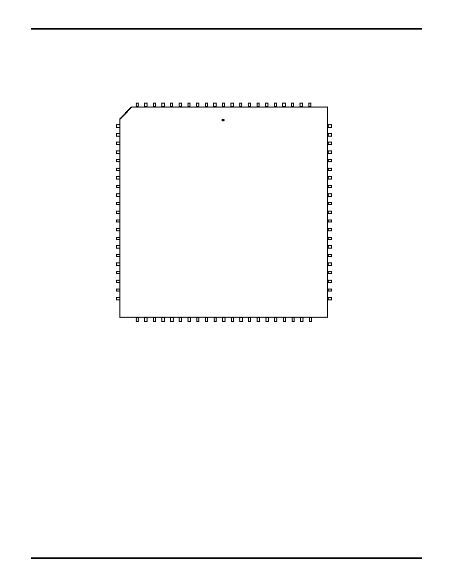
Figure 5. Z89391 84-Pin PLCC Pin Assignments
/P
A_EN
EXT15
PA
7
VSS
PA
6
EXT14
PA
5
EXT13
PA
4
EXT12
RXD
VSS
PA
3
EXT2
PA
2
EXT1
PA
1
EXT0
VSS
PA
0
VDD
12
32
VSS
PD0
EXT11
PD1
INT2
PD2
INT1
PD3
UI1
UI0
SCLK
VDD
RD//WR
PD4
W
AIT
PD5
/RESET
PD6
EA0
PD7
VDD
53
33
75
11
1
/EXTEN
EXT3
PA8
EXT4
PA9
VSS
EXT5
PA10
EXT6
PA11
EXT7
TXD
PA12
EXT8
PA13
EXT9
VSS
PA14
EXT10
PA15
VDD
74
54
VSS
PD15
FS1
PD14
UO1
PD13
UO0
PD12
INTO
FS0
HALT
PD11
CLK
/DS
PD10
VDD
PD9
EA2
PD8
EA1
/ROMEN
Z89391
84-Pin PLCC
Z89321/371/391
Zilog
16-Bit Digital Signal Processors
DS97DSP0100
P R E L I M I N A R Y
9
1
Table 4. Z89391 84-Pin PLCC Pin IdentiÞcation
No. Symbol
Function
Direction
1
RXD
Serial Input from CODEC
Input
2
EXT12
External Data 12
In/Output
3
PA4
Program Address 4
Output
4
EXT13
External Data 13
In/Output
5
PA5
Program Address 5
Output
6
EXT14
External Data 14
In/Output
7
PA6
Program Address 6
Output
8
V
SS
Ground
9
PA7
Program Address 7
Output
10
EXT15
External Data 15
In/Output
11
/PA_EN
Prog. Mem. Address Enable Input
12
/EXTEN
Ext. Bus Enable
Input
13
EXT3
External Data 3
In/Output
14
PA8
Program Address 8
Output
15
EXT4
External Data 4
In/Output
16
PA9
Program Address 9
Output
17
V
SS
Ground
18
EXT5
External Data 5
In/Output
19
PA10
Program Address 10
Output
20
EXT6
External Data 6
In/Output
21
PA11
Program Address 11
Output
22
EXT7
External Data 7
In/Output
23
TXD
Serial Output to CODEC
Output
24
PA12
Program Address 12
Output
25
EXT8
External Data 8
In/Output
26
PA13
Program Address 13
Output
27
EXT9
External Data 9
In/Output
28
V
SS
Ground
29
PA14
Program Address 14
Output
30
EXT10
External Data 10
In/Output
31
PA15
Program Address 15
Output
32
V
DD
Power Supply
Input
33
V
SS
Ground
34
PD0
Program Data 0
Input
35
EXT11
External Data 11
In/Output
36
PD1
Program Data 1
Input
37
INT2
User Interrupt 2
Input
38
PD2
Program Data 2
Input
39
INT1
User Interrupt 1
Input
40
PD3
Program Data 3
Input
41
UI1
User Input 1
Input
42
UI0
User Input 0
Input
43
SCLK
CODEC Interface Clock
In/Output
44
V
DD
Power Supply
Input
45
RD//WR
R/W External Bus
Output
46
PD4
Program Data 4
Input
47
WAIT
Wait State Input
Input
48
PD5
Program Data 5
Input
49
/RESET
Reset
Input
50
PD6
Program Data 6
Input
51
EA0
External Address 0
Output
52
PD7
Program Data 7
Input
53
V
DD
Power Supply
Input
54
/ROMEN
ROM Enable
Input
55
EA1
External Address 1
Output
56
PD8
Program Data 8
Input
57
EA2
External Address 2
Output
58
PD9
Program Data 9
Input
59
V
DD
Power Supply
Input
60
PD10
Program Data 10
Input
61
/DS
External Data Strobe
Output
62
CLK
Clock
Input
63
PD11
Program Data 11
Input
64
HALT
Stop Execution
Input
65
FS0
Frame Synch for CODEC
Interface 0
In/Output
66
INT0
User Interrupt 0
Input
67
PD12
Program Data 12
Input
68
UO0
User Output 0
Input
69
PD13
Program Data 13
Input
70
UO1
User Output 1
Input
71
PD14
Program Data 14
Input
72
FS1
Frame Synch for CODEC
Interface 1
In/Output
73
PD15
Program Data 15
Input
74
V
SS
Ground
75
V
DD
Power Supply
Input
76
PA0
Program Address 0
Output
77
V
SS
Ground
78
EXT0
External Data 0
In/Output
79
PA1
Program Address 1
Output
80
EXT1
External Data 1
In/Output
81
PA2
Program Address 2
Output
82
EXT2
External Data 2
In/Output
83
PA3
Program Address 3
Output
84
V
SS
Ground
Note: *Input or output is defined by interface mode selection.
Table 4. Z89391 84-Pin PLCC Pin IdentiÞcation
No. Symbol
Function
Direction

Z89321/371/391
16-Bit Digital Signal Processors
Zilog
10
P R E L I M I N A R Y
DS97DSP0100
ABSOLUTE MAXIMUM RATINGS
Stresses greater than those listed under Absolute Maxi-
mum Ratings may cause permanent damage to the de-
vice. This is a stress rating only; operation of the device at
any condition above those indicated in the operational sec-
tions of these specifications is not implied. Exposure to ab-
solute maximum rating conditions for extended periods
may affect device reliability.
STANDARD TEST CONDITIONS
The characteristics listed below apply for standard test
conditions as noted. All voltages are referenced to
Ground. Positive current flows into the referenced pin (Fig-
ure 6).
Symbol Description
Min.
Max. Units
V
CC
Supply voltage (*)
–0.3
+7.0
V
T
STG
Storage Temp.
–65
∞
+150
∞C
T
A
Oper. Ambient Temp.
∞C
Note:
* Voltage on all pins with respect to GND.
See Ordering Information.
Figure 6. Test Load Diagram
+5V
From Output
Under Test
30 pF
9.1 K
W
2.1 K
W

Z89321/371/391
Zilog
16-Bit Digital Signal Processors
DS97DSP0100
P R E L I M I N A R Y
11
1
DC ELECTRICAL CHARACTERISTICS
(V
DD
= 5V
±10%, T
A
= 0
∞C to +70∞C, unless otherwise noted.)
DC ELECTRICAL CHARACTERISTICS
(V
DD
= 5V 10%, T
A
= –40
∞C to +85∞C, unless otherwise specified)
fclock=20 MHz
1
fclock=16 MHz
2
fclock=24 MHz
3
Sym
Parameter
Condition
Min
Typ
Max.
Min
Typ
Max
Min
Typ
Max Units
I
DD
Supply
Current
V
DD
= 5.5V
70
55
85
mA
I
DC
DC Power Consumption
5
5
5
5
mA
V
IH
Input High Level
2.7
2.7
2.7
V
V
IL
Input Low Level
.8
.8
.8
V
I
L
Input Leakage
10
10
10
mA
V
OH
Output High Voltage
I
OH
=100
mA V
DD
-0.2
V
V
DD
-0.2
V
DD
-0.2
V
V
OL
Input Low Voltage
I
OL
=2.0 mA
.5
.5
.5
V
I
FL
Output Floating
Leakage Current
10
10
10
mA
Notes:
1. Z89321 and Z89391 only
2. Z89371 only. V
DD
= 5V,
± 5% for 16 MHz operation. V
DD
= 5V,
± 10% for 10 MHz operation.
3. Z89321 only. Limited availability. Contact Zilog sales office.
fclock = 20 MHz
1
Sym
Parameter
Condition
Min
Typ
Max
I
DD
Supply Current
V
DD
=5.5V
70
I
DC
DC Power Consumption
5
V
IH
Input High Level
2.7
V
IL
Input Low Level
.8
IL
Input Leakage
10
V
OH
Output High Voltage
I
OH
=100
mA
V
DD
-0.2
V
OL
Input Low Voltage
I
OL
=2.0 mA
.5
I
FL
Output Floating
Leakage Current
10
Notes:
1. Z89321 only
Z89321/371/391
16-Bit Digital Signal Processors
Zilog
12
P R E L I M I N A R Y
DS97DSP0100
AC ELECTRICAL CHARACTERISTICS
(V
DD
= 5V
±10%, T
A
= 0
∞C to +70∞C, unless otherwise specified.)
fclock = 20
MHz
1
fclock = 16 MHz
2
fclock = 24
MHz
3
Symbol
Parameter
Min
Max
Min
Max
Min
Max
Units
Clock
ns
TCY
Clock Cycle Time
50
6.25
41.7
ns
Tr
Clock Rise Time
2
2
2
ns
Tf
Clock Fall Time
2
2
2
ns
CPW
Clock Pulse Width
23
29
19
ns
I/O
DSVALID
/DS Valid Time from CLOCK Fall
0
15
0
15
0
15
ns
DSHOLD
/DS Hold Time from CLOCK Rise
4
15
4
15
4
15
ns
EASET
EA Setup Time to /DS Fall
12
12
12
ns
EAHOLD
EA Hold Time from /DS Rise
4
4
4
ns
RDSET
Data Read Setup Time to /DS Rise
14
14
14
ns
RDHOLD
Data Read Hold Time from /DS Rise
6
6
6
ns
WRVALID
Data Write Valid Time from /DS Fall
18
18
18
ns
WRHOLD
Data Write Hold Time from /DS Rise
5
5
5
ns
Interrupt
INTSET
Interrupt Setup Time to CLOCK Fall
7
7
7
ns
INTWIDTH
Interrupt Low Pulse Width
1 TCY
1 TCY
1 TCY
ns
CODEC Interface
SSET
SCLK Setup Time from Clock Rise
15
15
15
ns
FSSET
FSYNC Setup Time from SCLK Rise
6
6
6
ns
TXSET
TXD Setup Time from SCLK Rise
7
7
7
ns
RXSET
RXD Setup Time to SCLK Fall
7
7
7
ns
RXHOLD
RXD Hold Time from SCLK Fall
0
0
0
ns
Reset
RRISE
Reset Rise Time
1000
10000
1000
ns
RSET
Reset Setup Time to CLOCK Rise
15
15
15
ns
RWIDTH
Reset Low Pulse Width
2 TCY
2 TCY
2 TCY
ns
External Program Memory
PAVALID
PA Valid Time from CLOCK Rise
20
20
20
ns
PDSET
PD Setup Time to CLOCK Rise
10
10
10
ns
PDHOLD
PD Hold Time from CLOCK Rise
10
10
10
ns
Wait State
WSET
WAIT Setup Time to CLOCK Rise
23
23
23
ns
WHOLD
WAIT Hold Time from CLOCK Rise
1
1
1
ns
Halt
HSET
Halt Setup Time to CLOCK Rise
3
3
3
ns
HHOLD
Halt Hold Time from CLOCK Rise
10
10
10
ns
Notes:
1. Z89321 and Z89391 only
2. Z89371 only (V
DD
= 5V
± 5%)
3. Z89321 only. Limited availability. Contact Zilog sales office.
Z89321/371/391
Zilog
16-Bit Digital Signal Processors
DS97DSP0100
P R E L I M I N A R Y
13
1
AC ELECTRICAL CHARACTERISTICS
(V
DD
= 5V
±10%, T
A
= –40
∞C to +85∞C, unless otherwise specified.)
fclock = 20 MHz
1
Symbol
Parameter
Min
Max
Clock
TCY
Clock Cycle Time
50
Tr
Clock Rise Time
5
Tf
Clock Fall Time
5
CPW
Clock Pulse Width
20
I/O
DSVALID
/DS Valid Time from CLOCK Fall
0
18
DSHOLD
/DS Hold Time from CLOCK Rise
5
18
EASET
EA Setup Time to /DS Fall
15
EAHOLD
EA Hold Time from /DS Rise
5
RDSET
Data Read Setup Time to /DS Rise
17
RDHOLD
Data Read Hold Time from /DS Rise
8
WRVALID
Data Write Valid Time from /DS Fall
20
WRHOLD
Data Write Hold Time from /DS Rise
6
Interrupt
INTSET
Interrupt Setup Time to CLOCK Fall
9
INTWIDTH
Interrupt Low Pulse Width
1 TCY
CODEC Interface
SSET
SCLK Setup Time from Clock Rise
18
FSSET
FSYNC Setup Time from SCLK Rise
8
TXSET
TXD Setup Time from SCLK Rise
9
RXSET
RXD Setup Time to SCLK Fall
9
RXHOLD
RXD Hold Time from SCLK Fall
0
Reset
RRISE
Reset Rise Time
1000
RSET
Reset Setup Time to CLOCK Rise
18
RWIDTH
Reset Low Pulse Width
2 TCY
External Program Memory
PAVALID
PA Valid Time from CLOCK Rise
25
PDSET
PD Setup Time to CLOCK Rise
12
PDHOLD
PD Hold Time from CLOCK Rise
12
Wait State
WSET
WAIT Setup Time to CLOCK Rise
28
WHOLD
WAIT Hold Time from CLOCK Rise
2
Halt
HSET
Halt Setup Time to CLOCK Rise
4
HHOLD
Halt Hold Time from CLOCK Rise
12
Note:
1. Z89321 only

Z89321/371/391
16-Bit Digital Signal Processors
Zilog
14
P R E L I M I N A R Y
DS97DSP0100
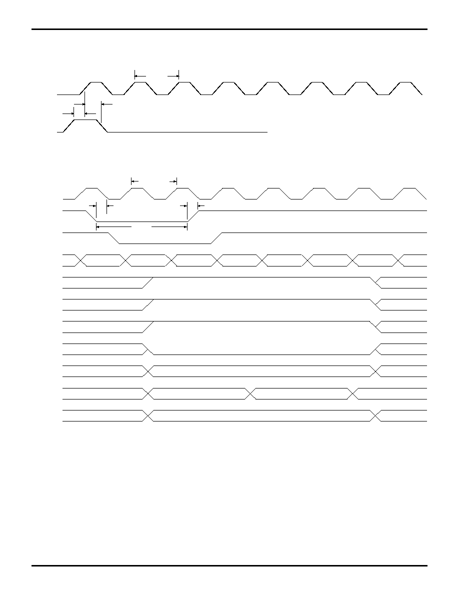
TIMING DIAGRAMS
Figure 7. Read Timing
TCY
Tr
Tf
CPW
DSHOLD
DSVALID
EASET
EAHOLD
RDSET
RDHOLD
Data In
Valid Address Out
CLOCK
/DS
EA(2:0)
RD//WR
EXT(15:0)
Figure 8. External (EXT) Bus Read Timing Using WAIT Pin
TCY
WSET
WHOLD
Valid Address Out
Data In
CLOCK
WAIT
/DS
EA(2:0)
RD//WR
EXT(15:0)
Z89321/371/391
16-Bit Digital Signal Processors
Zilog
15
P R E L I M I N A R Y
DS97DSP0100
TIMING DIAGRAMS (Continued)
Figure 9. Write Timing
TCY
DSHOLD
DSVALID
EASET
EAHOLD
WRVALID
WRHOLD
Data Out
Valid Address Out
EAHOLD
EASET
EXT(15:0)
RD//WR
EA(2:0)
/DS
CLOCK
Z89321/371/391
16-Bit Digital Signal Processors
Zilog
16
P R E L I M I N A R Y
DS97DSP0100
Figure 10. CODEC Interface Timing
TCY
SSET
FSSET
FSSET
TXSET
RXSET
RXHOLD
1
0
1
0
1
1
0
1
0
1
CLOCK
SCLK
FS0, FS1
TXD
RXD
Figure 11. Interrupt Timing
TCY
INTWidth
INTSET
Fetch N ≠1
Fetch N
Fetch N +1
Fetch Int_Addr
Fetch I
Fetch I +1
Execute N ≠1
Execute N
CALL Int Routine
Execute Int Routine
CLOCK
INT 0,1,2
PROGRAM
ADDRESS
EXECUTE
Z89321/371/391
16-Bit Digital Signal Processors
Zilog
17
P R E L I M I N A R Y
DS97DSP0100
TIMING DIAGRAMS (Continued)
Figure 12. HALT Timing
TCY
HHOLD
HSET
CLOCK
HALT
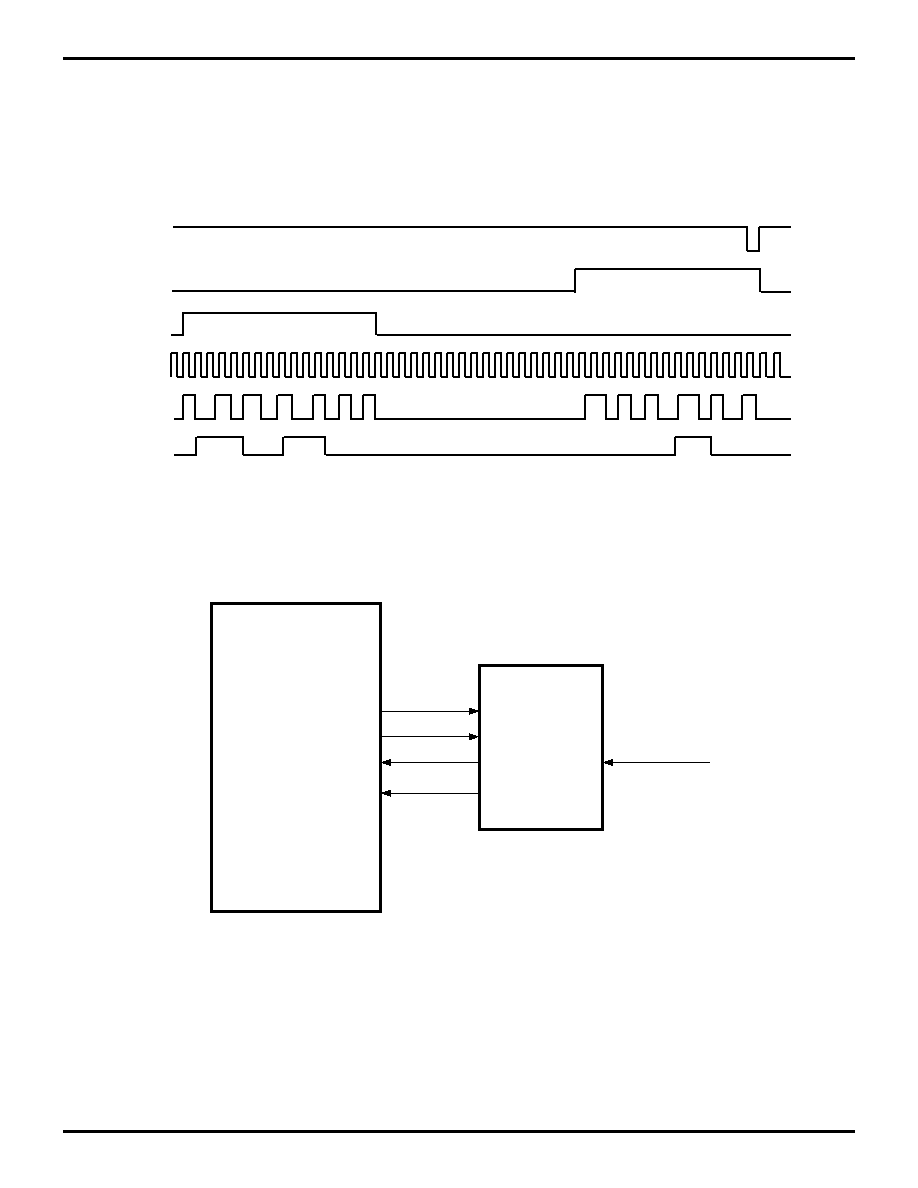
Figure 13. RESET Timing
Cycle 0
Cycle 1
Cycle 2
Cycle 3
Cycle 4
Cycle 5
Code Execution
Tri-Stated
Tri-Stated
Access Reset Vector
Intact*
* The RAM and hardware registers are left intact
during a warm reset. A cold reset will produce
random data in these locations. The status
register is set to zeroes in both cases.
CLOCK
/RESET
INTERNAL
RESET
EXECUTE
RD/WR
/DS
UO0-1
EA0-2
EXT0-15
PA0-15
RAM/
REGISTERS
TCY
RSET
RRISE
RWIDTH

Z89321/371/391
16-Bit Digital Signal Processors
Zilog
18
P R E L I M I N A R Y
DS97DSP0100
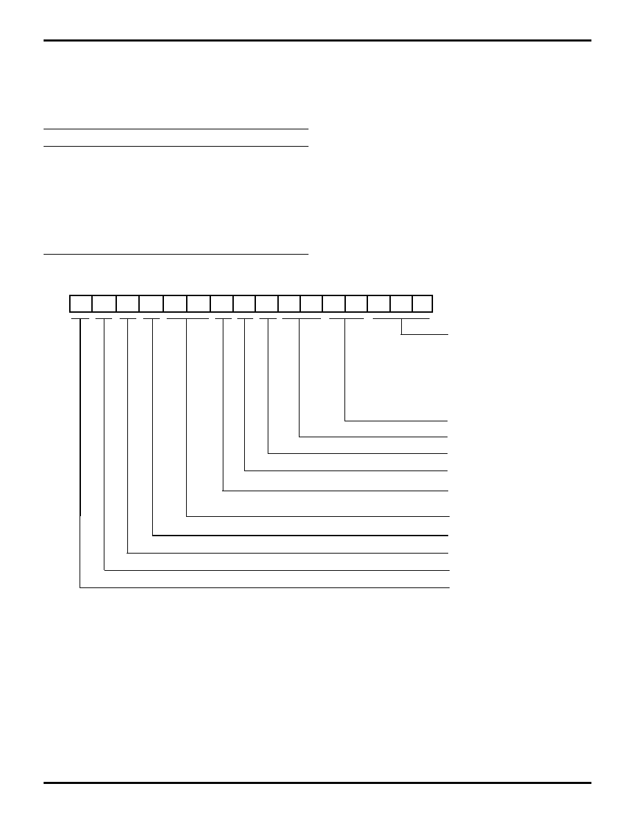
ADDRESS SPACE
Program Memory. Programs of up to 4 K words can be
masked into internal ROM (OTP for Z89371). Four loca-
tions are dedicated to the vector address for the three in-
terrupts (0FFDH-0FFFH) and the starting address follow-
ing a Reset (0FFCH). Internal ROM is mapped from 0000H
to 0FFFH, and the highest location for program is 0FFBH.
A 64 K word External Program Memory Space is available
on the Z89391. The vector addresses for the Z89391 re-
side at FFFCH-FFFFH (Figure 15).
Internal Data RAM. The Z89321, 371 and 391 all have in-
ternal 512 x 16-bit word data RAM organized as two banks
of 256 x 16-bit words each: RAM0 and RAM1. Each data
RAM bank is addressed by three pointers: Pn:0 (n = 0-2)
for RAM0 and Pn:1 (n = 0-2) for RAM1. The RAM address-
es for RAM0 and RAM1 are arranged from 0-255 and 256-
511, respectively. The address pointers, which may be
written to, or read from, are 8-bit registers connected to the
lower byte of the internal 16-bit D-Bus and are used to per-
form modulo addressing.
Three addressing modes are available to access the Data
RAM: register indirect, direct addressing, and short form
direct. The contents of the RAM can be read to, or written
from, in one machine cycle per word, without disturbing
any internal registers or status other than the RAM ad-
dress pointer used for each RAM. The contents of each
RAM can be loaded simultaneously into the X and Y inputs
of the multiplier.
Registers. The Z89321 has 19 internal registers and up to
an additional eight external registers. The external regis-
ters are user-definable for peripherals, such as A/D or D/A,
or to DMA, or other addressing peripherals. Both external
and internal registers are accessed in one machine cycle.
Figure 14. External Program Memory Port Timing
TCY
PDSET
PDHOLD
Valid
Valid
Valid
Valid
Valid
Valid
PASET
CLOCK
PROGRAM
ADDRESS
PROGRAM
DATA
Figure 15. Memory Map
Data Memory
Not Used
DRAM1
DRAM0
01FF
0100
00FF
0000
FFFF
Program Memory
Not Used
INT0-INT2 Vect.
RESET Vector
0FFF
0FFC
0000
FFFF
FFFC
4 Kwords
Or
INT0-INT2 Vect.
RESET Vector
64 Kwords
512 words
On-Chip Memory
Off-Chip Memory

Z89321/371/391
Zilog
16-Bit Digital Signal Processors
DS97DSP0100
P R E L I M I N A R Y
19
1
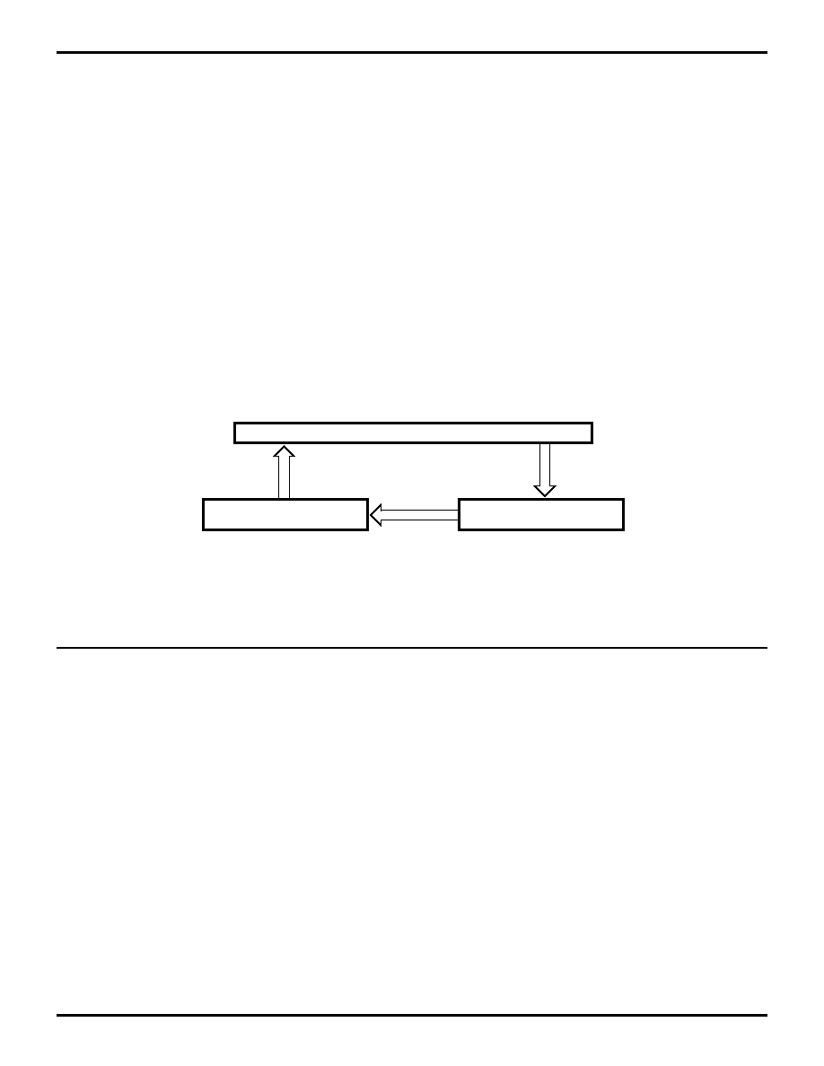
FUNCTIONAL DESCRIPTION
Instruction Timing. Most instructions are executed in one
machine cycle. Long immediate instructions and Jump or
Call instructions are executed in two machine cycles. A
multiplication or multiplication/accumulate instruction re-
quires a single cycle. Specific instruction cycle times are
described in the Condition Code section.
Multiply/Accumulate. The multiplier can perform a 16-bit
x 16-bit multiply, or multiply accumulate, in one machine
cycle using the Accumulator and/or both the X and Y in-
puts. The multiplier produces a 32-bit result, however, only
the 24 most significant bits are saved for the next instruc-
tion or accumulation. For operations on very small num-
bers where the least significant bits are important, the data
should first be scaled by eight bits (or the multiplier and
multiplicand by four bits each) to avoid truncation errors.
Note that all inputs to the multiplier should be fractional
two’s-complement, 16-bit binary numbers (Figure 16). This
puts them in the range [–1 to 0.9999695], and the result is
in 24 bits so that the range is [–1 to 0.9999999]. In addition,
if 8000H is loaded into both X and Y registers, the resulting
multiplication is considered an illegal operation as an over-
flow would result. Positive one cannot be represented in
fractional notation, and the multiplier will actually yield the
result 8000H x 8000H = 8000H (–1 x –1 = –1).
ALU. The ALU has two input ports, one of which is con-
nected to the output of the 24-bit Accumulator. The other
input is connected to the 24-bit P-Bus, the upper 16 bits of
which are connected to the 16-bit D-Bus. A shifter between
the P-Bus and the ALU input port can shift the data by
three bits right, one bit right, one bit left or no shift (Figure
17).
Figure 16. Multiplier Block Diagram
X Register (16)
Y Register (16)
Multiplier
P Register (24)
DDATA
XDATA
16
16
MUX
Shift Unit *
24
24
24
24
* Options:
1 Bit Right
3 Bits Right
No Shift
1 Bit Left
Figure 17. ALU Block Diagram
Arithmetic Logic Unit (ALU)
24
24
Accumulator (24)
24
* Options:
1 Bit Right
3 Bits Right
No Shift
1 Bit Left
DDATA
MUX
24
16
Mult. (24)
Shift Unit *
24
24

Z89321/371/391
16-Bit Digital Signal Processors
Zilog
20
P R E L I M I N A R Y
DS97DSP0100
Hardware Stack. A six-level hardware stack is connected
to the D-Bus to hold subroutine return addresses or data.
The Call instruction pushes PC+2 onto the stack, and the
RET instruction pops the contents of the stack to the PC.
User Inputs. The Z89321 has two inputs, UI0 and UI1,
which may be used by Jump and Call instructions. The
Jump or Call tests one of these pins and if appropriate,
jumps to a new location. Otherwise, the instruction be-
haves like a NOP. These inputs are also connected to the
status register bits S10 and S11, which may be read by the
appropriate instruction (Figure 8).
User Outputs. The status register bits S5 and S6 connect
directly to UO0 and UO1 pins and may be written to by the
appropriate instruction. Note: The user output value is the
opposite of the status register content.
Interrupts. The Z89321 has three positive edge-triggered
interrupt inputs. An interrupt is acknowledged at the end of
an instruction execution. It takes two machine cycles to en-
ter an interrupt instruction sequence. The PC is pushed
onto the stack. A RET instruction transfers the contents of
the stack to the PC and decrements the stack pointer by
one word. The priority of the interrupts is INT0 = highest,
INT2 = lowest. INT1 is dedicated to the CODEC interface
and INT2 is dedicated to the 13-bit timer if both peripherals
are enabled. Note: The SIEF instruction enables the inter-
rupts. The SIEF instruction must be used before exiting an
interrupt routine since the interrupts are automatically dis-
abled when entering the routine.
Registers. The Z89321 has 19 physical internal registers
and up to eight user-defined external registers. The EA2-
EA0 determines the address of the external registers. The
signals are used to read from or write to the external reg-
isters /DS, WAIT, RD//WR.
I/O Bus. The processor provides a 16-bit, CMOS-compat-
ible bus. I/O Control pins provide convenient communica-
tion capabilities with external peripherals, and single-cycle
access is possible. For slower communications, an on-
board hardware wait-state generator can be used to ac-
commodate timing conflicts. Three latched I/O address
pins are used to access external registers. The EXT 4, 5,
6, 7 pins are used by the internal peripherals. Disabling a
peripheral allows access to these addresses for general-
purpose use.
CODEC Interface. The multi-compatible, dual CODEC in-
terface provides the necessary control signals for trans-
mission of CODEC information to the DSP processor. The
interface accommodates 8-bit PCM or 16-bit Linear CO-
DECs. Special compatibility with Crystal Semiconductor's
4215/4216 CODECs provides the necessary interface for
audio applications. Many general-purpose 8-, 16-bit A/Ds,
D/As are adaptable. The interface can also be used as a
high-speed serial port.
m-Law Compression. The 8-bit CODEC interface mode
provides
m-law compression from 13-bit format to 8-bit for-
mat. Decompression is performed in software by use of a
128-word lookup table.
Timer. Two programmable timers are available. One is
dedicated to the CODEC interface, the other for general-
purpose use. When a time-out event occurs, an interrupt
request is generated. Single pass and/or continuous
modes are available. If the CODEC interface is not used,
both timers can be used for general-purpose.
Note: Wait-State Generator. An internal wait-state
generator is provided to accommodate slow external
peripherals. A single wait-state can be implemented
through control registers EXT7-2. For additional states, a
dedicated pin (WAIT) can be held High. The WAIT pin is
monitored only during execution of a read or write
instruction to external peripherals (EXT bus).
Note: A WAIT pin is not available on the 40-pin DIP
package.

Z89321/371/391
Zilog
16-Bit Digital Signal Processors
DS97DSP0100
P R E L I M I N A R Y
21
1
REGISTERS
The internal registers are defined below:
The following are virtual registers as physical RAM does
not exist on the chip.
P holds the result of multiplications and is read-only.
X and Y are two 16-bit input registers for the multiplier.
These registers can be utilized as temporary registers
when the multiplier is not being used.
A is a 24-bit Accumulator. The output of the ALU is sent to
this register. When 16-bit data is transferred into this reg-
ister, it is placed into the 16 MSBs and the least significant
eight bits are set to zero. Only the upper 16 bits are trans-
ferred to the destination register when the Accumulator is
selected as a source register in transfer instructions.
Pn:b are the pointer registers for accessing data RAM, (n
= 0,1,2 refer to the pointer number) (b = 0,1 refers to RAM
Bank 0 or 1). They can be directly read from or written to,
and can point to locations in data RAM or Program Mem-
ory.
EXTn are external registers (n = 0 to 7). There are eight
16-bit registers provided here for mapping external devic-
es into the address space of the processor. Note that the
actual register RAM does not exist on the chip, but would
exist as part of the external device, such as an ADC result
latch. Use of the CODEC interface and 13-bit timer reduc-
es the number of external registers to four.
BUS is a read-only register which, when accessed, returns
the contents of the D-Bus. Bus is used for emulation only.
Dn:b refers to locations in RAM that can be used as a
pointer to locations in program memory which is efficient
for coefficient addressing. The programmer decides which
location to choose from two bits in the status register and
two bits in the operand. Thus, only the lower 16 possible
locations in RAM can be specified. At any one time, there
are eight usable pointers, four per bank, and the four point-
ers are in consecutive locations in RAM.
For example, if S3/S4 = 01 in the status register, then
D0:0/D1:0/D2:0/D3:0 refer to register locations 4/5/6/7 in
RAM Bank 0. Note that when the data pointers are being
written to, a number is actually being loaded to Data RAM,
so they can be used as a limited method for writing to
RAM.
SR is the status register, which contains the ALU status
and certain control bits (Table 5).
Register Register
DeÞnition
P
Output of Multiplier, 24-bit
X
X Multiplier Input, 16-bit
Y
Y Multiplier Input, 16-bit
A
Accumulator, 24-bit
SR
Status Register, 16-bit
Pn:b
Six Ram Address Pointers, 8-bit each
PC
Program Counter, 16-bit
EXT4
13-Bit Timer ConÞguration Register
EXT5-1
CODEC Interface Channel 0 Data
EXT5-2
CODEC Interface Channel 0 Data
EXT6-1
CODEC Interface Channel 1 Data
EXT6-2
CODEC Interface Channel 1 Data
EXT7-1
CODEC Interface ConÞguration Register
EXT7-2
Wait-State Generator/CODEC Interface
ConÞguration Register
Register Register
DeÞnition
EXTn
External Registers, 16-bit
BUS
D-Bus
Dn:b
Eight Data Pointers*
Note: * These occupy the first four locations in RAM bank.
Table 5. Status Register Bit Functions
Status Register Bit
Function
S15 (N)
ALU Negative
S14 (OV)
ALU Overþow
S13 (Z)
ALU Zero
S12 (L)
Carry
S11 (UI1)
User Input 1
S10 (UI0)
User Input 0
S9 (SH3)
MPY Output Arithmetically
Shifted Right by Three Bits
S8 (OP)
Overþow Protection
S7 (IE)
Interrupt Enable
S6 (UO1)
User Output 1
S5 (UO0)
User Output 0
S4-S3
“Short Form Direct” bits
S2-S0 (RPL)
RAM Pointer Loop Size
Z89321/371/391
16-Bit Digital Signal Processors
Zilog
22
P R E L I M I N A R Y
DS97DSP0100
The status register can always be read in its entirety. S15-
S10 are set/reset by hardware and can only be read by
software. S9-S0 control hardware looping and can be writ-
ten by software (Table 6).
S15-S12 are set/reset by the ALU after an operation. S11-
S10 are set/reset by the user inputs. S6-S0 are control bits
described in Table 5. S7 enables interrupts. If S8 is set, the
hardware clamps at maximum positive or negative values
instead of overflowing. If S9 is set and a multiple/shift op-
tion is used, then the shifter shifts the result three bits right.
This feature allows the data to be scaled and prevents
overflows.
PC is the Program Counter. When this register is assigned
as a destination register, one NOP machine cycle is added
automatically to adjust the pipeline timing.
External Register, EXT4-EXT7, are used by the CODEC
interface and 13-bit timer, the registers are reviewed in the
CODEC interface section.
Table 6. RPL Description
S2
S1
S0
Loop Size
0
0
0
256
0
0
1
2
0
1
0
4
0
1
1
8
1
0
0
16
1
0
1
32
1
1
0
64
1
1
1
128
Figure 18. Status Register
0 0 0
0 0 1
0 1 0
0 1 1
1 0 0
1 0 1
1 1 0
1 1 1
256
2
4
8
16
32
64
128
"Short Form Direct" bits
User Output 0-1*
Interrupt Enable
Overflow protection
MPY output arithmetically shifted
right by three bits
User Input 0-1 (Read Only)
Carry
Zero
Overflow
Negative
Ram Pointer Loop Size
* The output value is the opposite of the status register content.
S7
S6
S5
S4
S3
S2
S1
S0
S15
S14
S13
S12
S11
S10
S9
S8
N
OV
Z
C
UI1
UI0
SH3
OP
IE
UO1 UO0
RPL
Z89321/371/391
Zilog
16-Bit Digital Signal Processors
DS97DSP0100
P R E L I M I N A R Y
23
1
PERIPHERAL OPERATION
Disabling Peripherals
Disabling a peripheral (CODEC Interface, Counter) allows
general-purpose use of the EXT address for the disabled
peripheral. If the peripheral is not disabled, the EXT control
signals and EXT data are still provided, but transfer of data
on the EXT pins is not available (because internal transfers
are being processed on the internal bus). Care must be
taken to ensure that control of the EXT bus does not cause
bus conflicts.
Reading Data from CODEC Interface*
External data is serially transferred into the CODEC inter-
face registers from an external CODEC. This serial data is
loaded into EXT5-2 (8- or 16-bit modes). Because the in-
terface is double-buffered, data must be transferred to
EXT5-1 before being transferred along the internal data
bus of the processor. This is accomplished by writing data
to EXT5-2.
Writing Data to CODEC Interface
Internal data is transferred from the internal data bus of the
processor to the EXT5-2 register. The CODEC interface
constantly transfers and receives data during normal oper-
ation. Data to be transferred is loaded to EXT5-2 and is au-
tomatically serially transferred.
Note: EXT5-1 and EXT5-2 are used in the example, but
this information applies equally to EXT6-1 and EXT6-2.
(Refer to Figure 20, CODEC Block Diagram.)
LOADING EXT7
Because EXT7 is double-buffered, a pair of writes are per-
formed when loading the EXT7 registers (Figure 19).
Interrupts
The Z89321 features three interrupts:
If all peripherals are enabled, INT0 (general-purpose) can
be used.
Figure 19. EXT7 Register ConÞguration
Internal 16-Bit Bus
Wait-State Register
16
EXT7-1
EXT7-2
16
CODEC Timer Register
EXT7-1
EXT7-2
LD EXT7, #%54F4
Loads CODEC Timer Register
LD EXT7, #%6CDA
Loads Wait-State Register
LD @P0:0, EXT7
Reads EXT7-1 and places
data in RAM
INT0
General-Purpose
INT1
CODEC Interface
INT2
13-Bit Timer

Z89321/371/391
16-Bit Digital Signal Processors
Zilog
24
P R E L I M I N A R Y
DS97DSP0100
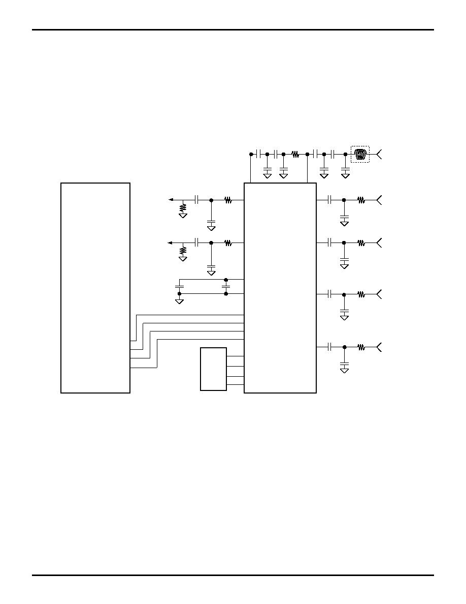
CODEC Interface
The CODEC Interface provides direct-connect capabilities
for standard 8-, 16-bit CODECs. The interface also sup-
ports 8-bit PCM, 8-bit PCM with hardware
m-law conver-
sion (
m-law expansion is done in software), 16-bit Linear
and Crystal's Sigma-Delta Stereo CODEC modes. Regis-
ters are used to accommodate the CODEC Interface
(EXT5, EXT6 and EXT7). The CODEC interface provides
two Frame Sync signals, which allows two channels of
data for transmission/receiving.
CODEC Interface Hardware
The CODEC Interface hardware uses six 16-bit registers,
m-law compression logic and general-purpose logic to con-
trol transfers to the appropriate register (Figure 20).
CODEC Interface Control Signals
SCLK (Serial Clock)
The Serial Clock provides a clock signal for operating the
external CODEC. A 4-bit prescaler is used to determine
the frequency of the output signal.
Note: An internal divide-by-two is performed before the
clock signal is passed to the Serial Clock prescaler.
SCLK = (0.5* CLK)/PS
where: CLK = System Clock
PS = 4-bit Prescaler*
* The Prescaler is an up-counter.
Figure 20. CODEC Interface Block Diagram
m
-Law
Compression
Data Bus
16
16
16
16
16
16
CLKIN
TXD
EXT5-2
CLKIN
CLKIN
CLKIN
CLKIN
EXT5-1
EXT6-1
EXT6-2
CONTROL
LOGIC
RXD
EXT7-1
EXT7-2
16
Z89321/371/391
Zilog
16-Bit Digital Signal Processors
DS97DSP0100
P R E L I M I N A R Y
25
1
TXD (Serial Output to CODEC)
The TXD line provides 8-, 16-, and 64-bit data transfers.
Each bit is clocked out of the processor by the rising edge
of the SCLK, with the MSB transmitted first.
RXD (Serial Input from CODEC)
The RXD line provides 8-, 16-, and 64-bit data transfers.
Each bit is clocked into the processor by the falling edge of
the SCLK, with the MSB received first.
FS0, FS1 (Frame Sync)
The Frame Sync is used for enabling data transfer/receive.
The rising and falling edge of the Frame Sync encloses the
serial data transmission.
Interrupt
Once the transmission of serial data is completed an inter-
nal interrupt signal is initiated. A single-cycle Low pulse al-
lows an interrupt on INT1. When this occurs, the processor
will jump to the defined Interrupt 1 vector location (Figure
21).
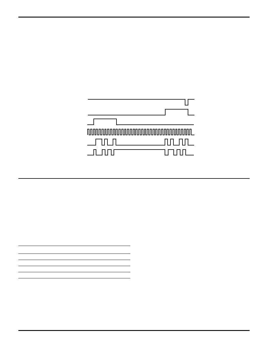
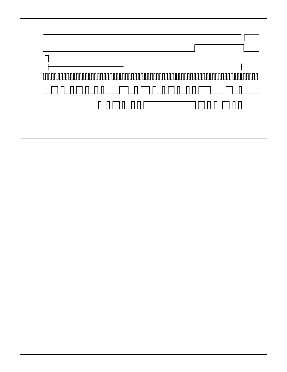
CODEC INTERFACE TIMING
Figure 21 depicts a typical 8-bit serial data transfer using
both of the CODEC Interface Channels. The transmitting
data is clocked out on the rising edge of the SCLK signal.
An external CODEC clocks data in on the falling edge of
the SCLK signal. Once the serial data is transmitted, an in-
terrupt is given. The CODEC interface signals are not initi-
ated if the CODEC interface is not enabled.
The following modes are available for FSYNC and SCLK
signals:
The CODEC interface timing is independent of the proces-
sor clock when external mode is chosen. This feature pro-
vides the capability for an external device to control the
transfer of data to the Z89321. The Frame Sync signal en-
velopes the transmitted data, therefore care must be taken
to ensure proper sync signal timing (Figure 21).
Full Duplex Operation
The Transmit and Receive lines are used for transfer of se-
rial data to or from the CODEC interface. The CODEC in-
terface performs both data transmit and receive simulta-
neously.
Control Registers
The CODEC interface is double-buffered, therefore, four
registers are provided for CODEC interface data storage.
EXT5-1 and EXT5-2 operate with the Frame Sync 0 while
EXT6-1 and EXT6-2 operate with Frame Sync 1. In 8- or
16-bit mode, the CODEC interface uses EXT5-1 and
EXT6-1. For Stereo mode, all four registers are used (Fig-
ures 22 and 23).
The CODEC Interface Control Register (EXT7-1) is shown
in Figure 14. Setting of the CODEC mode, FSYNC, and
Enable/Disable of CODEC 0 is done through this register.
The Wait-State Generator, SCLK, and CODEC 1 are con-
trolled from EXT7-2 (Figure 24).
Figure 21. CODEC Interface Timing (8-Bit Mode)
int1_
fs1
sclk
fs0
txd
rxd
SCLK
FSYNC
Internal
Internal
External
External
External
Internal
Internal
External

Z89321/371/391
16-Bit Digital Signal Processors
Zilog
26
P R E L I M I N A R Y
DS97DSP0100
Figure 22. CODEC Interface Data Registers (Channel 0)
D15 D14 D13
D11 D10 D9 D8
D12
D7 D6 D5 D4 D3 D2
D1 D0
5-1
Data Bits 15-0
D15 D14 D13
D11 D10 D9 D8
D12
D7 D6 D5 D4 D3 D2
D1 D0
5-2
Data Bits 15-0
Figure 23. CODEC Interface Data Registers (Channel 1)
D15 D14 D13
D11 D10 D9 D8
D12
D7 D6 D5 D4 D3 D2
D1 D0
6-1
Data Bits 15-0
D15 D14 D13
D11 D10 D9 D8
D12
D7 D6 D5 D4 D3 D2
D1 D0
6-2
Data Bits 15-0

Z89321/371/391
Zilog
16-Bit Digital Signal Processors
DS97DSP0100
P R E L I M I N A R Y
27
1
REGISTERS
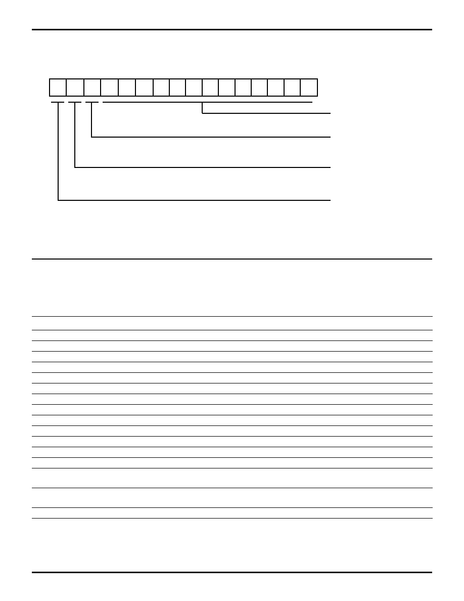
Figure 24. CODEC Interface Control Register
D7
D6
D5
D4
D3
D2
D1
D0
D15
D14
D13
D12
D11
D10
D9
D8
SCLK Prescaler (up-counter)
EXT7-1
SCLK/FSYNC Ratio Prescaler (up-counter)
CODEC Mode
00 8-bit with hardware
m
-law
01 8-bit without hardware
m
-law
10 16-bit linear
11 Crystal CS4215 / CS4216
FSYNC
0 External Source*
1 Internal Source
CODEC 0 Disable/Enable
0 = Disable*
1 = Enable
Note: The timer is an up-counter.
Example: EXT7-1 = #%x00D OSC = 12.288 MHz, SCLK = 2.048 MHz, FSYNC = 8 kHz
EXT7-1 = #%x80F OSC = 12.288 MHz, SCLK = 6.144 MHz, FSYNC = 48 kHz
EXT7-1 = #%xFFx No interrupt
EXT7-1 = #%x000 Max interrupt period (667
m
s for OSC = 12.288 MHz)
* Default

Z89321/371/391
16-Bit Digital Signal Processors
Zilog
28
P R E L I M I N A R Y
DS97DSP0100
Figure 25. WSG, SCLK and CODEC Interface Control Register
D7
D6
D5
D4
D3
D2
D1
D0
D15
D14
D13
D12
D11
D10
D9
D8
EXT7-2
Wait State EXT0
Wait State EXT1
Wait State EXT2
Wait State EXT3
Wait State EXT4
Wait State EXT5
Wait State EXT6
SCLK
0 External Source*
1 Internal Source
CODEC 1 Disable/Enable
0 = Disable*
1 = Enable
nws - no wait states
ws - one wait states
00 no wait states (nws)
01 read (nws), write (ws)
10 read (ws), write (nws)
11 read (ws), write (ws)
*Default

Z89321/371/391
Zilog
16-Bit Digital Signal Processors
DS97DSP0100
P R E L I M I N A R Y
29
1
A/D Accommodation
The CODEC interface can be used for serial A/D or serial
D/A transmission. The interface provides the necessary
control signals to adapt to many standard serial convert-
ers. The low-pass and smoothing filters are necessary for
systems with converters.
High-Speed Serial Port
The Z89321 CODEC interface can be used as a high-
speed serial port. The necessary control signals are pro-
vided for adaptation to standard processors or external pe-
ripherals. Byte, word, or 64-bit data can be transmitted at
speeds up to 10 Mbps. (Condition includes a 20 MHz os-
cillator. Data can be transferred with single-cycle instruc-
tions to an internal register file.)
8-Bit CODEC Interface
The Z89321 provides an option for a standard 8-bit CO-
DEC interface. Hardware
m-law compression is available
(expansion performed by software lookup table). The CO-
DEC interface transmits data consisting of 8-bit or com-
pounded 8-bit information. Figure 27 shows a typical sche-
matic arrangement.
The timing for this type of arrangement is presented in Fig-
ure 28. The flexible design provides adaptation for 16-bit
linear CODEC.
Figure 26. A/D, D/A Implementation Block Diagram
SCLK
Communicate
Data
Serial
Data In
CLKIN
FSO
FS1
TXD
Serial A/D
Serial
Data Out
Low-Pass
Filter
Analog
In
CLKIN
Communicate
Data
Smoothing
Filter
Analog
Out
RXD
Serial A/D
Z89321/371/391
Table 7. Tabulated Transmission Rates*
Transmission
Rate
Maximum SCLK
10 Mbps
Maximum Frame Sync
8-bit
769.2 kHz
16-bit
476.2 kHz
Stereo (64-bit)
263.2 kHz
Note: Calculations consider the interrupt access time (typically
four cycles), transfer of data, loading of new data, and latency pe-
riods between CODEC transfers. During the interrupt cycle, de-
velopers often execute additional software, affecting the
maximum transfer rate. Calculations are for single-channel trans-
fers only.

Z89321/371/391
16-Bit Digital Signal Processors
Zilog
30
P R E L I M I N A R Y
DS97DSP0100
Figure 27. 8-Bit CODEC Schematic
VDD
RXD
TXD
SCLK
FS1
RDD
15
DC
CCI
TDD
TDE
VLS
9
10
16
14
RCE
11
12
13
VCC
Z89321
/371
/391
VAG
Rx0
Txl
+Tx
≠Tx
Mu/A
PDI
VSS
≠5V
1
2
3
4
5
6
7
8
VCC
Analog
In
Analog
Out
5k
10k
GND
MC145505p
Figure 28. 8-Bit Mode Timing Diagram
int1_
fs1
fs0
txd
rxd
sclk
Z89321/371/391
Zilog
16-Bit Digital Signal Processors
DS97DSP0100
P R E L I M I N A R Y
31
1
16-Bit Linear CODEC Interface
For higher precision transmissions, a 16-bit linear CODEC
is used, however, data is not compressed in this mode of
transmission. The Z89321 provides accommodation for
two channels of 16-bit transmission (Figure 29).
For data acquisition systems, designers may opt for a 16-
bit serial A/D. A block diagram of the Z89321 with the
AD1876 16-bit 100 Kbps sampling ADC is shown in Figure
30.
Figure 29. 16-Bit Mode Timing Diagram
int1_
fs1
sclk
fs0
txd
rxd
Figure 30. 16-Bit Mode Timing Diagram
16-Bit A/D
Anti-Alias
Filtered
Analog
Signal
AD 1876
Z89321/371/391
Busy
Dout
CLK
Sample
FS1
RxD
SCLK
UO0
Vin
Z89321/371/391
16-Bit Digital Signal Processors
Zilog
32
P R E L I M I N A R Y
DS97DSP0100
Stereo CODEC Interface
The Z893XX DSP product family CODEC interface pro-
vides direct connection to other CODECs for master or
slave modes, supporting 64 bits of transmission data (16
bits right channel, 16 bits left channel, and 32 bits of con-
figuration information). This configuration information con-
sists of input gain, input MUX, output attenuation, ADC
clipping, and mute and error functions of the CODECs.
A key feature of the Z893XX DSP product family is that it
adapts easily to other stereo CODECs, including Crystal
Semiconductor's CS4215 and CS4216 devices (Figure
31).
The 64 bits of data transferred from the CODEC are placed
in four registers, EXT5-1, 5-2, 6-1, and 6-2 (Figure 32 ).
Figure 31. Z893XX and CS4216 CODEC Interface
Z89321
/371/391
SCLK
FS0
TxD
RxD
Channel 2
Input
Channel 1
Input
Channel 1
Input
150
150
150
0.47
m
F
0.47
m
F
0.47
m
F
0.01
m
F
NPO
0.01
m
F
NPO
0.01
m
F
NPO
LIN1
RIN1
LIN2
LOUT
600
16
0.0022
m
F
NPO
+
≥
1.0
m
F
40k
27
27
28
CS4216
REFBYP
REFGND
21
22
0.1
m
F
10
m
F
+
Audio
Out
(Right)
150
0.47
m
F
0.01
m
F
NPO
Channel 2
Input
RIN2
ROUT
600
0.0022
m
F
NPO
15
+
≥
1.0
m
F
40k
26
+5V
Supply
VD
1
m
F
+
VA
24
0.1
m
F
4
1
m
F +
0.1
m
F
Audio
Out
(Left)
2.0
Ferrite Bead
43
42
44
SDOUT
SDIN
SSYNC
SCLK
1
SMODE2
SFS1
SFS2
SMODE1
Mode
Setting
32
31
30
29
Z89321/371/391
Zilog
16-Bit Digital Signal Processors
DS97DSP0100
P R E L I M I N A R Y
33
1
16-Bit General-Purpose Timer
The 13-bit counter/timer is available for general-purpose
use. When the counter counts down to the zero state, an
interrupt is received on INT2. If the counter is disabled,
EXT4 can be used as a general-purpose address. The
counting operation of the counter can be disabled by reset-
ting bit 14. Selection of the clock source allows the ability
to extend the counter value past the 13 bits available in the
control register. Use of the CODEC counter output can ex-
tend the counter to 26 bits (see Figure 33).
Note: Placing zeroes into the count value register does
not generate an interrupt. Therefore, it is possible to have
a single-pass option by loading the counter with zeroes
after the start of count.
The counter is defaulted to the enable state, but if it is not
needed, it can be disabled. However, once disabled, the
counter cannot be enabled unless a reset of the processor
is performed.
Example:
Figure 32. CODEC Stereo Mode Timing Diagram
64 bits transferred
int1_
fs1
fs0
sclk
txd
rxd
LD EXT, #%C008 ;1100 0000 0000 1000
; Enable Counter
; Enable Counting
; Clock Source = OSC/2
; Count Value = 1000 = 8
; Interrupt will occur every
16 clock cycles
Z89321/371/391
16-Bit Digital Signal Processors
Zilog
34
P R E L I M I N A R Y
DS97DSP0100
ADDRESSING MODES (Continued)
ADDRESSING MODES
This section discusses the syntax of the addressing
modes supported by the DSP assembler.
Figure 33. CODEC Timer Register
D7
D6
D5
D4
D3
D2
D1
D0
D15
D14
D13
D12
D11
D10
D9
D8
EXT4
Count Value (Down-Counter)
Clock Source
Count Operation
Counter
0 Oscillator/2*
1 CODEC Counter Output
0 = Disable*
1 = Enable
0 = Disable
1 = Enable*
* Default State
Table 8. Addressing Modes
Symbolic Name
Syntax
Description
<pregs>
Pn:b
Pointer Register
<dregs> (Points to RAM)
Dn:b
Data Register
<hwregs>
X,Y,PC,SR,P , EXTn, A, BUS Hardware Registers
<accind> (Points to Program Memory
@A
Accumulator Memory Indirect
<direct>
<expression>
Direct Address Expression
<limm>
#<const exp>
Long (16-bit) Immediate Value
<simm>
#<const exp>
Short (8-bit) Immediate Value
<regind> (Points to RAM)
@Pn:b
Pointer Register Indirect
@Pn:b+
Pointer Register Indirect with Increment
@Pn:b–LOOP
Pointer Register Indirect with Loop Decrement
@Pn:b+LOOP
Pointer register Indirect with Loop Increment
<memind> (Points to Program Memory) @@Pn:b
Pointer Register Memory Indirect
@Dn:b
Data Register Memory Indirect
@@Pn:b–LOOP
Pointer Register Memory Indirect with Loop
Decrement
@@Pn:b+LOOP
Pointer Register Memory Indirect with Loop
Increment
@@Pn:b+
Pointer Register Memory Indirect with Increment
Z89321/371/391
Zilog
16-Bit Digital Signal Processors
DS97DSP0100
P R E L I M I N A R Y
35
1
There are eight distinct addressing modes for data trans-
fer.
<pregs>, <hwregs> These two modes are used for sim-
ple loads to and from registers within the chip, such as
loading to the Accumulator, or loading from a pointer reg-
ister. The names of the registers need only be specified in
the operand field (destination first, then source).
<regind> This mode is used for indirect accesses to the
data RAM. The address of the RAM location is stored in
the pointer. The “@” symbol indicates “indirect” and pre-
cedes the pointer, therefore @P1:1 instructs the processor
to read or write to a location in RAM1, which is specified by
the value in the pointer.
<dregs> This mode is also used for accesses to the data
RAM, but only the lower 16 addresses in either bank. The
4-bit address comes from the status register and the oper-
and field of the data pointer. Note that data registers are
typically used not for addressing RAM, but loading data
from program memory space.
<memind> This mode is used for indirect accesses to the
program memory. The address of the memory is located in
a RAM location, which is specified by the value in a point-
er. Therefore, @@P1:1 instructs the processor to read
(write is not possible) from a location in memory, which is
specified by a value in RAM, and the location of the RAM
is in turn specified by the value in the pointer. Note that the
data pointer can also be used for a memory access in this
manner, but only one “@” precedes the pointer. In both
cases, the memory address stored in RAM is incremented
by one, each time the addressing mode is used, to allow
easy transfer of sequential data from program memory.
<accind> Similar to the previous mode, the address for
the program memory read is stored in the Accumulator.
@A in the second operand field loads the number in mem-
ory specified by the address in A.
<direct> The direct mode allows read or write to data
RAM from the Accumulator by specifying the absolute ad-
dress of the RAM in the operand of the instruction. A num-
ber between 0 and 255 indicates a location in RAM0, and
a number between 256 and 511 indicates a location in
RAM1.
<limm> This address mode indicates a long immediate
load. A 16-bit word can be copied directly from the operand
into the specified register or memory.
<simm> This address mode can only be used for imme-
diate transfer of 8-bit data in the operand to the specified
RAM pointer.
CONDITION CODES
The following Instruction Description defines the condition
codes supported by the DSP assembler.
If the instruction description refers to the <cc> (condition
code) symbol in one of its addressing modes, the instruc-
tion will only execute if the condition is true.
Code
Description
C
Carry
EQ
Equal (same as Z)
F
False
IE
Interrupts Enabled
MI
Minus
NC
No Carry
NE
Not Equal (same as NZ)
NIE
Not Interrupts Enabled
NOV
Not Overþow
NU0
Not User Zero
Code
Description
NU1
Not User One
NZ
Not zero
OV
Overþow
PL
Plus (Positive)
U0
User Zero
U1
User One
UGE
Unsigned Greater Than or
Equal (Same as NC)
ULT
Unsigned Less Than (Same as C)
Z
Zero
Z89321/371/391
16-Bit Digital Signal Processors
Zilog
36
P R E L I M I N A R Y
DS97DSP0100
PACKAGE INFORMATION
Figure 34. 40-Pin Package Diagram
Figure 35. 44-Pin PLCC Package Diagram

Z89321/371/391
Zilog
16-Bit Digital Signal Processors
DS97DSP0100
P R E L I M I N A R Y
37
1
Figure 36. 44-Pin QFP Package Diagram
Figure 37. 84-Pin PLCC Package Diagram
Z89321/371/391
16-Bit Digital Signal Processors
Zilog
38
P R E L I M I N A R Y
DS97DSP0100
ORDERING INFORMATION
For fast results, contact your local Zilog sales office for assistance in ordering the part desired.
CODES
Package
P= Plastic DIP
V = Plastic PLCC
F = Plastic QFP
Temperature
S = 0
∞C to +70∞C
E = -40
∞C to 85∞C
Speed
20 = 20 MHz
16 = 16 MHz
Environmental
C = Plastic Standard
Z89321
Z89371
Z89391
20 MHz
16 MHz
20 MHz
44-Pin PLCC
44-pin PLCC
84-Pin PLCC
Z8932120VSC
Z8937116VSC
Z8939120VSC
20 MHz
16 MHz
40-Pin DIP
40-Pin DIP
Z8932120PSC
Z8937116PSC
20 MHz
16 MHz
44-Pin QFP
44-Pin QFP
Z8932120FSC
Z8937116FSC
Example:
Z 89321 20 V S C
Environmental Flow
Temperature
Package
Speed
Product Number
Zilog Prefix
is a Z89321, 20 MHz, PLCC, 0
∞C to +70∞C, Plastic Standard Flow

Z89321/371/391
Zilog
16-Bit Digital Signal Processors
DS97DSP0100
P R E L I M I N A R Y
39
1
© 1997 by Zilog, Inc. All rights reserved. No part of this
document may be copied or reproduced in any form or by
any means without the prior written consent of Zilog, Inc.
The information in this document is subject to change
without notice. Devices sold by Zilog, Inc. are covered by
warranty and patent indemnification provisions appearing
in Zilog, Inc. Terms and Conditions of Sale only. Zilog, Inc.
makes no warranty, express, statutory, implied or by
description, regarding the information set forth herein or
regarding the freedom of the described devices from
intellectual property infringement. Zilog, Inc. makes no
warranty of merchantability or fitness for any purpose.
Zilog, Inc. shall not be responsible for any errors that may
appear in this document. Zilog, Inc. makes no commitment
to update or keep current the information contained in this
document.
Zilog’s products are not authorized for use as critical
components in life support devices or systems unless a
specific written agreement pertaining to such intended use
is executed between the customer and Zilog prior to use.
Life support devices or systems are those which are
intended for surgical implantation into the body, or which
sustains life whose failure to perform, when properly used
in accordance with instructions for use provided in the
labeling, can be reasonably expected to result in
significant injury to the user.
Zilog, Inc. 210 East Hacienda Ave.
Campbell, CA 95008-6600
Telephone (408) 370-8000
FAX 408 370-8056
Internet: http://www.zilog.com

Z89321/371/391
16-Bit Digital Signal Processors
Zilog
40
P R E L I M I N A R Y
DS97DSP0100