 | –≠–ª–µ–∫—Ç—Ä–æ–Ω–Ω—ã–π –∫–æ–º–ø–æ–Ω–µ–Ω—Ç: Z89393 | –°–∫–∞—á–∞—Ç—å:  PDF PDF  ZIP ZIP |

1
Z89323/373/393
16-B
IT
D
IGITAL
S
IGNAL
P
ROCESSORS
P R E L I M I N A R Y
DS95DSP0101 Q4/95
FEATURES
P
RELIMINARY
C
USTOMER
P
ROCUREMENT
S
PECIFICATION
DSP ROM
OTP
DSP RAM
Max Core
Device
(K Words) (K Words)
(Words)
MIPS
Z89323
8
512
2 0
Z89373
8
512
1 6
Z89393
64*
512
2 0
* External
Package
44-Pin
68-Pin
44-Pin
80-Pin
100-Pin
Device
PLCC
PLCC
QFP
QFP
QFP
Z89323
Z89373
Z89393
s
Operating Temperature Ranges:
0
∞
C to +70
∞
C (Standard)
≠40
∞
C to +85
∞
C (Extended)
s
4.5- to 5.5-Volt Operating Range
DSP Core
s
20 MIPS @ 20 MHz, 16-Bit Fixed Point DSP
s
50 ns Instruction Cycle Time
s
Single-Cycle Multiply and ALU Operations
s
Two Internal Data Buses and Address Generators
s
Six Register Address Pointers
s
Optimized Instruction Set (30 Instructions)
On-Board Peripherals
s
4-Channel, 8-Bit Analog to Digital Converter (A/D)
s
On-Board Serial Peripheral Interface (SPI)
s
Up to 40 Bits of Programmable I/O
s
Two Channels of Programmable
Pulse Width Modulators (PWM)
s
Three General-Purpose Timer/Counters
s
Two Watch-Dog Timers (WDT)
s
Programmable PLL
s
Three Vectored Interrupts Servicing Eight
Interrupt Sources
s
Power-Down and Power-On Reset
GENERAL DESCRIPTION
The Z89323/373/393 DSP family of products builds on
Zilog's first generation Z893XX DSP core, integrating several
peripherals especially well suited for cost-effective voice,
telephony, and control applications.
These DSP devices feature a modified Harvard architecture
supported by one program bus and two on-chip data
buses. This bus structure is supported by two address
generators and six register pointers to ensure that the
20 MIPS DSP CPU is continually active.
The Z893X3 DSP family is designed to provide a complete
DSP and control system on a single chip. By integrating
various peripherals, such as a high-speed 4-channel, 8-bit
A/D, an SPI, three timers with PWM and WDT support, the
Z893X3 family provides a compact system solution and
reduces overall system cost.
To support a wide variety of development needs, the
Z893X3 DSP product family features the cost-effective
Z89323 with 8 Kwords of on-chip ROM, and the Z89373, a
16-MIPS OTP version of the Z89323, ideal for prototypes
and early production builds. For systems requiring more
than 8 Kwords of program memory, the Z89393 device can
address up to 64 Kwords of external program memory.
Z89323/373/393
16-B
IT
D
IGITAL
S
IGNAL
P
ROCESSORS

Z89323/373/393
16-B
IT
D
IGITAL
S
IGNAL
P
ROCESSORS
2
P R E L I M I N A R Y
DS95DSP0101 Q4/95
GENERAL DESCRIPTION
(Continued)
The Z893X3 DSP family is 100 percent source and object-
code compatible with the existing Z89321/371/391 devices,
providing users, who can benefit from increased integration
and reduced system cost, an easy migration path from one
DSP product to the next.
Throughout this specification, references to the Z89323
device applies equally to the Z89373 and Z89393, unless
otherwise specified.
Notes:
All Signals with a preceding front slash, "/", are active Low, e.g.,
B//W (WORD is active Low); /B/W (BYTE is active Low, only).
Power connections follow conventional descriptions below:
Connection
Circuit
Device
Power
V
CC
V
DD
Ground
GND
V
SS
Figure 1. Z893X3 Functional Block Diagram
Program
ROM/OTP
8192x16
Data RAM0
256x16
EA0-2
EXT0-15/P00-15
/DS
WAIT
RD//WR
Data RAM1
256x16
DDATA
XDATA
PDATA
PADDR
PD0-15
PA0-15
Shifter
Arithmetic
Logic Unit
(ALU)
Program
Control
Unit
CLKO
HALT
/ROMEN
/RES
Accumulator
Port 1
P10-17
or
INT2
CLKOUT
SIN
SOUT
SK
SS
UI0-1
X
Y
Multiplier
P
DP0-3
DP4-6
P2
P2
P1
P1
P0
P0
ADDR
GEN0
ADDR
GEN1
8-Bit
A/D
AN0
AN1
AN2
AN3
16-Bit
Program
I/O
Port 0
8-Bit I/O
CLKI
/PAZ
VALI
AGND
ANVCC
VALO
VSS
VDD
/EXTEN
8-Bit I/O
Port 2
P20-27
UI2
UO0-2
INT0-1
or
16-Bit Timer,
Counter
16-Bit Timer,
Counter, PWM
16-Bit Timer,
Counter, PWM
SPI
Port 3
P30-33
P34-37
4 Inputs
4 Outputs

3
Z89323/373/393
16-B
IT
D
IGITAL
S
IGNAL
P
ROCESSORS
P R E L I M I N A R Y
DS95DSP0101 Q4/95
PIN DESCRIPTION
No.
Symbol
Function
Direction
1
P20/INT0
Port 2 0/Interrupt 0
In/Output
2
EXT12/P012
Ext Data 12/Port 0 12
In/Output
3
EXT13/P013
Ext Data 13/Port 0 13
In/Output
4
EXT14/P014
Ext Data 14/Port 0 14
In/Output
5
V
SS
Ground
6
EXT15/P015
Ext Data 15/Port 0 15
In/Output
7
EXT3/P03
Ext Data 3/Port 0 3
In/Output
8
EXT4/P04
Ext Data 4/Port 0 4
In/Output
9
V
SS
Ground
10
EXT5/P05
Ext Data 5/Port 0 5
In/Output
11
EXT6/P06
Ext Data 6/Port 0 6
In/Output
12
EXT7/P07
Ext Data 7/Port 0 7
In/Output
13
P21/INT1
Port 2 1/Interrupt 1
In/Output
14
EXT8/P08
Ext Data 8/Port 0 8
In/Output
15
EXT9/P09
Ext Data 9/Port 0 9
In/Output
16
V
SS
Ground
17
EXT10/P010
Ext Data 10/Port 0 10
In/Output
18
EXT11/P011
Ext Data 11/Port 0 11
In/Output
19
VAHI
Analog High Ref.
Input
20
VALO
Analog Low Ref.
Input
21
ANGND
Analog Ground
Input
22
AN0
A/D Input 0
Input
No.
Symbol
Function
Direction
23
AN1
A/D Input 1
Input
24
AN2
A/D Input 2
Input
25
AN3
A/D Input 3
Input
26
ANVCC
Analog Power
Input
27
V
DD
Power
28
RD//WR
R/W External Bus
Output
29
EA0
Ext Address 0
Output
30
EA1
Ext Address 1
Output
31
EA2
Ext Address 2
Output
32
P23/UO1
Port 2 3/User Output 1
In/Output
33
/DS
Ext Data Strobe
Output
34
CLKI
Clock/Crystal In
Input
35
CLKO
Clock/Crystal Out
Input
36
P22/UO0
Port 2 2/User Output 0
In/Output
37
P24/UO2
Port 2 4/User Output 2
In/Output
38
WAIT
Wait for Ext
Input
39
/RES
Reset
Input
40
V
SS
Ground
41
EXT0/P00
Ext Data 0/Port 0 0
In/Output
42
EXT1/P01
Ext Data 1/Port 0 1
In/Output
43
EXT2/P02
Ext Data 2/Port 0 2
In/Output
44
V
SS
Ground
Figure 2. 44-Pin PLCC Z89323/373 Pin Configuration
Table 1. 44-Pin PLCC Z89323/373 Pin Description
6
Z89323/373
44-Pin PLCC
EXT3/P03
5
4
3
2
1
44 43 42 41 40
18 19 20 21 22 23 24 25 26 27 28
7
8
9
10
11
12
13
14
15
16
17
39
38
37
36
35
34
33
32
31
30
29
EXT4/P04
VSS
EXT5/P05
EXT6/P06
EXT7/P07
INT1/P21
EXT8/P08
EXT9/P09
VSS
EXT10/P010
/RES
WAIT
P24/UO2
P22/UO0
CLKO
CLKI
/DS
P23/UO1
EA2
EA1
EA0
EXT1
1/P01
1
V
AHI
V
ALO
ANGND
AN0
AN1
AN2
AN3
ANVCC
VDD
RD//WR
EXT15/P015
VSS
EXT14/P014
EXT13/P013
EXT12/P012
P20/INT0
VSS
EXT2/P02
EXT1/P01
EXT0/P00
VSS

Z89323/373/393
16-B
IT
D
IGITAL
S
IGNAL
P
ROCESSORS
4
P R E L I M I N A R Y
DS95DSP0101 Q4/95
PIN DESCRIPTION
(Continued)
Figure 3. 68-Pin PLCC Z89323/373 Pin Configuration
Z89323/373
68-Pin PLCC
7
8
9
6
5
4
3
2
1
10
11
12
13
14
15
16
17
18
19
20
21
22
23
24
25
26
68 67 66 65 64 63 62 61
27 28 29 30 31 32 33 34 35 36 37 38 39 40 41 42 43
60
59
58
57
56
55
54
53
52
51
50
49
48
47
46
45
44
EXT1
1/P01
1
VDD
V
AHI
VSS
UI0/P16
V
ALO
UI1/P17
AGND
AN0
AN1
AN2
AN3
VSS
P21/INT1
ANVCC
VDD
RD//WR
VSS
/RES
WAIT
P25/UI2
P22/UO0
P26
CLKO
CLKI
P24/UO2
/DS
P23/UO1
VDD
NC
EA2
EA1
EA0
HALT
NC
EXT3/P03
EXT4/P04
VSS
VDD
EXT5/P05
SOUT/P13
EXT6/P06
SS/P14
EXT7/P07
SK/P15
P27
EXT8/P08
EXT9/P09
VSS
EXT10/P010
VSS
NC
EXT15/P015
VSS
EXT14/P014
VDD
EXT13/P013
EXT12/P012
P20/INT0
P12/SIN
P1
1/CLKOUT
VSS
P10
EXT2/P02
EXT1/P01
EXT0/P00
VSS
VDD
5
Z89323/373/393
16-B
IT
D
IGITAL
S
IGNAL
P
ROCESSORS
P R E L I M I N A R Y
DS95DSP0101 Q4/95
Table 2. 68-Pin PLCC Z89323/373 Pin Description
No.
Symbol
Function
Direction
1
P12/SIN
Port 1 2/Serial Input
In/Output
2
P20/INT0
Port 2 0/Interrupt 0
In/Output
3
EXT12/P012
Ext Data 12/Port 0 12
In/Output
4
EXT13/P013
Ext Data 13/Port 0 13
In/Output
5
VDD
Power
6
EXT14/P014
Ext Data 14/Port 0 14
In/Output
7
V
SS
Ground
8
EXT15/P015
Ext Data 15/Port 0 15
In/Output
9
NC
No Connection
10
NC
No Connection
11
EXT3/P03
Ext Data 3/Port 0 3
In/Output
12
EXT4/P04
Ext Data 4/Port 0 4
In/Output
13
V
SS
Ground
14
V
DD
Power
15
EXT5/P05
Ext Data 5/Port 0 5
In/Output
16
P13/SOUT
Port 1 3/Serial Output
In/Output
17
EXT6/P06
Ext Data 6/Port 0 6
In/Output
18
P14/SS
Port 1 4/Serial Select
In/Output
19
EXT7/P07
Ext Data 7/Port 0 7
In/Output
20
P15/SK
Port 1 5/Serial Clock
In/Output
21
P27
Port 2 7
In/Output
22
EXT8/P08
Ext Data 8/Port 0 8
In/Output
23
EXT9/P09
Ext Data 9/Port 0 9
In/Output
24
V
SS
Ground
25
EXT10/P010
Ext Data 10/Port 0 10
In/Output
26
V
SS
Ground
27
EXT11/P011
Ext Data 11/Port 0 11
In/Output
28
V
DD
Power
29
VAHI
Analog High Ref.
Input
30
V
SS
Ground
31
P16/UI0
Port 1 6/User Input 0
In/Output
32
VALO
Analog Low Ref.
Input
33
P17/UI1
Port 1 7/User Input 1
In/Output
34
ANGND
Analog Ground
Input
No.
Symbol
Function
Direction
35
AN0
A/D Input 0
Input
36
AN1
A/D Input 1
Input
37
AN2
A/D Input 2
Input
38
AN3
A/D Input 3
Input
39
V
SS
Ground
40
P21/INT1
Port 2 1/Interrupt 1
In/Output
41
ANVCC
Analog Power
Input
42
V
DD
Power
Input
43
RD//WR
R/W External Bus
Output
44
HALT
Halt Execution
Input
45
EA0
Ext Address 0
Output
46
EA1
Ext Address 1
Output
47
EA2
Ext Address 2
Output
48
NC
No Connection
49
V
DD
Power
50
P23/UO1
Port 2 3/User Output 1
In/Output
51
/DS
Ext Data Strobe
Output
52
P24/UO2
Port 2 4/User Output 2
In/Output
53
CLKI
Clock/Crystal In
Input
54
CLKO
Clock/Crystal Out
Input
55
P26
Port 2 6
In/Output
56
P22/UO0
Port 2 2/User Output 0
In/Output
57
P25/UI2
Port 2 5/User Input 2
In/Output
58
WAIT
Wait for Ext
Input
59
/RES
Reset
Input
60
V
SS
Ground
61
V
DD
Power
62
V
SS
Ground
63
EXT0/P00
Ext Data 0/Port 0 0
In/Output
64
EXT1/P01
Ext Data 1/Port 0 1
In/Output
65
EXT2/P02
Ext Data 2/Port 0 2
In/Output
66
P10/INT2
Port 1 0/Interrupt 2
In/Output
67
V
SS
Ground
68
P11/CLKOUT
Port 1 1/Clock Output
In/Output
Z89323/373/393
16-B
IT
D
IGITAL
S
IGNAL
P
ROCESSORS
6
P R E L I M I N A R Y
DS95DSP0101 Q4/95
PIN DESCRIPTION
(Continued)
EXT15/P015
VSS
EXT14/P014
EXT13/P013
P20/INT0
VSS
EXT2/P02
EXT1/P01
EXT0/P00
VSS
EXT1
1/P01
1
V
AHI
V
ALO
ANGND
AN0
AN1
AN2
AN3
ANVCC
VDD
RD//WR
/RES
WAIT
P24/UO2
P22/UO0
CLK0
CLK1
/DS
P23/UO1
EA2
EA1
EA0
EXT3/P03
EXT4/P04
VSS
EXT5/P05
EXT6/P06
EXT7/P07
INT1/P21
EXT8/P08
EXT9/P09
VSS
EXT10/P010
1
2
3
4
5
6
7
8
9
10
11
32
31
30
29
28
27
26
25
24
23
33
Z89323/373
44-Pin QFP
44 43 42 41 40 39 38 37 36 35 34
12 13 14 15 16 17 18 19 20 21 22
EXT12/P012
No.
Symbol
Function
Direction
1
EXT3/P03
Ext Data 3/Port 0 3
In/Output
2
EXT4/P04
Ext Data 4/Port 0 4
In/Output
3
V
SS
Ground
4
EXT5/P05
Ext Data 5/Port 0 5
In/Output
5
EXT6/P06
Ext Data 6/Port 0 6
In/Output
6
EXT7/P07
Ext Data 7/Port 0 7
In/Output
7
P21/INT1
Port 2 1/Interrupt 1
In/Output
8
EXT8/P08
Ext Data 8/Port 0 8
In/Output
9
EXT9/P09
Ext Data 9/Port 0 9
In/Output
10
V
SS
Ground
11
EXT10/P010
Ext Data 10/Port 0 10
In/Output
12
EXT11/P011
Ext Data 11/Port 0 11
In/Output
13
VAHI
Analog High Ref.
Input
14
VALO
Analog Low Ref.
Input
15
ANGND
Analog Ground
Input
16
AN0
A/D Input 0
Input
17
AN1
A/D Input 1
Input
18
AN2
A/D Input 2
Input
19
AN3
A/D Input 3
Input
20
ANVCC
Analog Power
Input
21
V
DD
Power
22
RD//WR
R/W External Bus
Output
No.
Symbol
Function
Direction
23
EA0
Ext Address 0
Output
24
EA1
Ext Address 1
Output
25
EA2
Ext Address 2
Output
26
P23/UO1
Port 2 3/User Output 1
In/Output
27
/DS
Ext Data Strobe
Output
28
CLKI
Clock/Crystal In
Input
29
CLKO
Clock/Crystal Out
Input
30
P22/UO0
Port 2 2/User Output 0
In/Output
31
P24/UO2
Port 2 4/User Output 2
In/Output
32
WAIT
Wait for Ext
Input
33
/RES
Reset
Input
34
V
SS
Ground
35
EXT0/P00
Ext Data 0/Port 0 0
In/Output
36
EXT1/P01
Ext Data 1/Port 0 1
In/Output
37
EXT2/P02
Ext Data 2/Port 0 2
In/Output
38
V
SS
Ground
39
P20/INT0
Port 2 0/Interrupt 0
In/Output
40
EXT12/P012
Ext Data 12/Port 0 12
In/Output
41
EXT13/P013
Ext Data 13/Port 0 13
In/Output
42
EXT14/P014
Ext Data 14/Port 0 14
In/Output
43
V
SS
Ground
44
EXT15/P015
Ext Data 15/Port 0 15
In/Output
Table 3. 44-Pin QFP Z89323/373 Pin Description
Figure 4. 44-Pin QFP Z89323/373 Pin Configuration
7
Z89323/373/393
16-B
IT
D
IGITAL
S
IGNAL
P
ROCESSORS
P R E L I M I N A R Y
DS95DSP0101 Q4/95
Figure 4a. 80-Pin QFP Z89323/373 Pin Configuration
41
RD//WR
42
P35
43
NC
44
HALT
45
EA0
46
P36
47
EA1
48
EA2
49
NC
50
VCC
51
P23/U01
53
P24/U02
54
CLKI
55
CLKO
56
P26
57
P22/UO0
59
WAIT
52
/DS
60
P37
58
P25/UI2
NC
EXT15/P015
/EXTEN
NC
EXT3/P03
P32
EXT4/P04
VSS
VCC
EXT5/P05
P13/SOUT
1
2
3
4
5
6
7
8
9
10
11
Z89323
80-Pin QFP
EXT6/P06
P14/SS
EXT7/P07
P15/SK
P27
EXT8/P08
EXT9/P09
VSS
P33
12
13
14
15
16
17
18
19
20
61
/RES
62
VSS
63
VCC
64
NC
65
VSS
66
P30
67
EXT0/P00
68
EXT1/P01
69
EXT2/P02
70
P10/INT2
71
VSS
73
P12/SIN
74
P20/INT0
75
EXT12/P012
76
EXT13/P013
77
VCC
79
VSS
72
P1
1/CLKOUT
80
P31
78
EXT14/P014
EXT10/P010
VSS
NC
P34
EXT1
1/P01
1
VCC
V
AHI
VSS
P16/UI0
V
AL0
P17/UI1
21
22
23
24
25
26
27
28
29
30
31
ANGND
AN0
AN1
AN2
AN3
VSS
INT1/P21
ANVCC
VCC
32
33
34
35
36
37
38
39
40

Z89323/373/393
16-B
IT
D
IGITAL
S
IGNAL
P
ROCESSORS
8
P R E L I M I N A R Y
DS95DSP0101 Q4/95
PIN DESCRIPTION
(Continued)
Table 4a. 80-Pin QFP Z89323/373 Pin Description
No.
Symbol
Function
Direction
1
NC
No Connection
2
EXT15/P015
Ext Data 15/Port 0 15
In/Output
3
/EXTEN
Ext Enable
Input
4
NC
No Connection
5
EXT3/P03
Ext Data 3/Port 0 3
In/Output
6
P32
Port3 2
Input
7
EXT4/P04
Ext Data 4/Port 0 4
In/Output
8
V
SS
Ground
9
V
DD
Power
10
EXT5/P05
Ext Data 5/Port 0 5
In/Output
11
P13/SOUT
Port 1 3/Serial Output
In/Output
12
EXT6/P06
Ext Data 6/Port 0 6
In/Output
13
P14/SS
Port 1 4/Serial Select
In/Output
14
EXT7/P07
Ext Data 7/Port 0 7
In/Output
15
P15/SK
Port 1 5/Serial Clock
In/Output
16
P27
Port 2 7
In/Output
17
EXT8/P08
Ext Data 8/Port 0 8
In/Output
18
EXT9/P09
Ext Data 9/Port 0 9
In/Output
19
V
SS
Ground
20
P33
Port 3 3
Input
21
EXT10/P010
Ext Data 10/Port 0 10
In/Output
22
V
SS
Ground
23
NC
No Connection
24
P34
Port 3 4
Output
25
EXT11/P011
Ext Data 11/Port 0 11
In/Output
26
V
DD
Power
27
VAHI
Analog High Ref.
Input
28
V
SS
Ground
29
P16/UI0
Port 1 6/User Input 0
In/Output
30
VAL0
Analog Low Ref.
Input
31
P17/UI1
Port 1 7/User Input 1
In/Output
32
ANGND
Analog Ground
Input
33
AN0
A/D Input 0
Input
34
AN1
A/D Input 1
Input
35
AN2
A/D Input 2
Input
36
AN3
A/D Input 3
Input
37
V
SS
Ground
38
P21/INT1
Port 2 1/Interrupt 1
In/Output
39
ANVCC
Analog Power
Input
40
V
DD
Power
Input
No.
Symbol
Function
Direction
41
RD//WR
R/W External Bus
Output
42
P35
Port 3 5
Output
43
NC
No Connection
44
HALT
Halt Execution
Input
45
EA0
Ext Address 0
Output
46
P36
Port 3 6
Output
47
EA1
Ext Address 1
Output
48
EA2
Ext Address 2
Output
49
NC
No Connection
50
V
DD
Power
51
P23/UO1
Port 2 3/User Output 1
In/Output
52
/DS
Ext Data Strobe
Output
53
P24/UO2
Port 2 4/User Output 2
In/Output
54
CLKI
Clock/Crystal In
Input
55
CLKO
Clock/Crystal Out
Input
56
P26
Port 2 6
In/Output
57
P22/UO0
Port 2 2/User Output 0
In/Output
58
P25/UI2
Port 2 5/User Input 2
In/Output
59
WAIT
Wait for Ext
Input
60
P37
Port 3 7
Output
61
/RES
Reset
Input
62
V
SS
Ground
63
V
DD
Power
64
NC
No Connection
65
V
SS
Ground
66
P30
Port 3 0
Input
67
EXT0/P00
Ext Data 0/Port 0 0
In/Output
68
EXT1/P01
Ext Data 1/Port 0 1
In/Output
69
EXT2/P02
Ext Data 2/Port 0 2
In/Output
70
P10/INT2
Port 1 0/Interrupt 2
In/Output
71
V
SS
Ground
72
P11/CLKOUT
Port 1 1/Clock Output
In/Output
73
P12/SIN
Port 1 2/Serial Input
In/Output
74
P20/INT0
Port 2 0/Interrupt 0
In/Output
75
EXT12/P012
Ext Data 12/Port 0 12
In/Output
76
EXT13/P013
Ext Data 13/Port 0 13
In/Output
77
V
DD
Power
78
EXT14/P014
Ext Data 14/Port 0 14
In/Output
79
V
SS
Ground
80
P31
Port 3 1
Input
9
Z89323/373/393
16-B
IT
D
IGITAL
S
IGNAL
P
ROCESSORS
P R E L I M I N A R Y
DS95DSP0101 Q4/95
/EXTEN
EXT3/P03
PA8
EXT4/P04
PA9
VSS
VDD
EXT5/P05
PA10
SOUT/P13
EXT6/P06
1
2
3
4
5
6
7
8
9
10
11
Z89393
100-Pin QFP
PA11
SS/P14
EXT7/P07
SK/P15
P27
PA12
EXT8/P08
PA13
EXT9/P09
PA14
VSS
12
13
14
15
16
17
18
19
20
21
22
PA15
EXT10/P010
VSS
23
24
25
PD0
EXT1
1/P01
1
PD1
VDD
V
AHI
VSS
UI0/P16
V
ALO
UI1/P17
PD2
ANGND
26
27
28
29
30
31
32
33
34
35
36
AN0
AN1
AN2
AN3
VSS
INT1/P21
ANVCC
PD3
VDD
PD4
PD5
37
38
39
40
41
42
43
44
45
46
47
RD//WR
PD6
PD7
48
49
50
51
HALT
52
EA0
53
PD8
54
EA1
55
PD9
56
EA2
57
/ROMEN
58
VDD
59
PD10
60
P23/UO1
61
/DS
62
PD11
63
P24/UO2
64
CLKI
65
CLKO
66
P26
68
P22/UO0
69
PD13
70
P25/UI2
71
PD14
72
WAIT
74
/RES
67
PD12
75
VSS
73
PD15
76
VDD
77
VSS
78
PA
0
79
EXT0/P00
80
PA
1
81
EXT1/P01
82
PA
2
83
EXT2/P02
84
P10/INT2
85
PA
3
86
VSS
87
P1
1/CLKOUT
88
P12/SIN
89
P20/INT0
90
PA
4
91
EXT12/P012
93
EXT13/P013
94
VDD
95
EXT14/P14
96
PA
6
97
VSS
99
EXT15/P015
92
PA
5
100
/P
AZ
98
PA
7
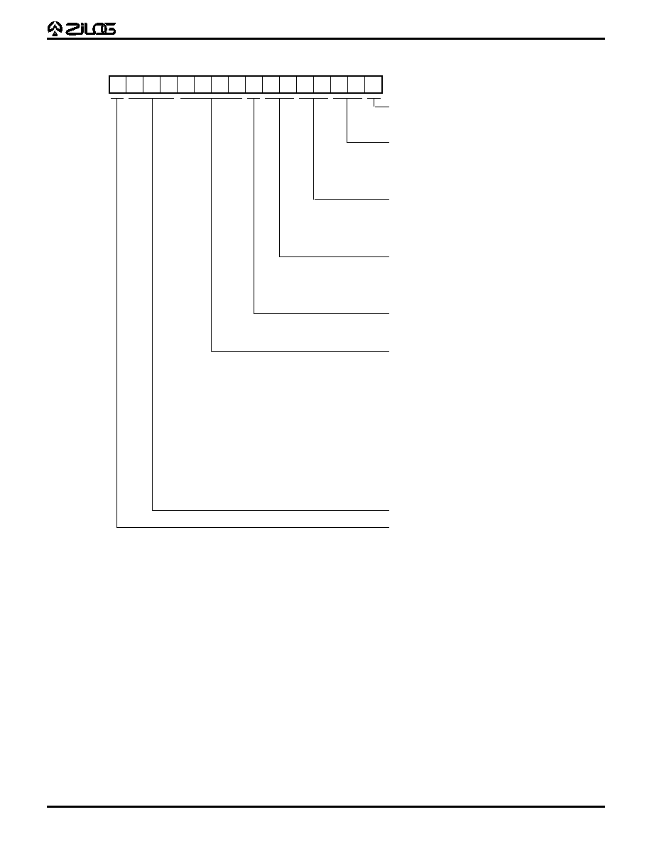
Figure 5. 100-Pin QFP Z89393 Pin Configuration

Z89323/373/393
16-B
IT
D
IGITAL
S
IGNAL
P
ROCESSORS
10
P R E L I M I N A R Y
DS95DSP0101 Q4/95
PIN DESCRIPTION
(Continued)
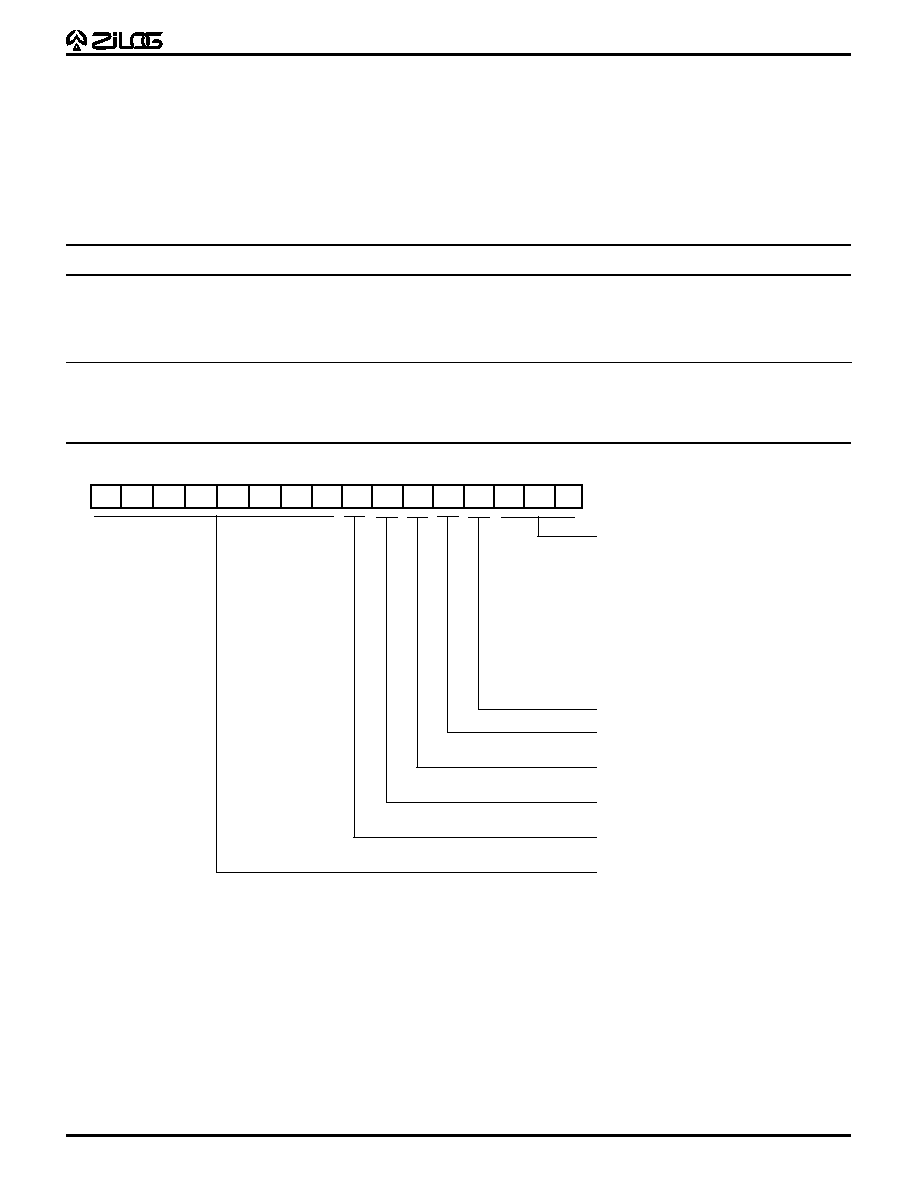
Table 4. 100-Pin QFP Z89393 Pin Description
No.
Symbol
Function
Direction
1
/EXTEN
EXT Enable
Input
2
EXT3/P03
Ext Data 3/Port 0 3
In/Output
3
PA8
Program Address 8
Output
4
EXT4/P04
Ext Data 4/Port 0 4
In/Output
5
PA9
Program Address 9
Output
6
V
SS
Ground
7
V
DD
Power
8
EXT5/P05
Ext Data 5/Port 0 5
In/Output
9
PA10
Program Address 10
Output
10
P13/SOUT
Port 1 3/Serial Output
In/Output
11
EXT6/P06
Ext Data 6/Port 0 6
In/Output
12
PA11
Program Address 11
Output
13
P14/SS
Port 1 4/Serial Select
In/Output
14
EXT7/P07
Ext Data 7/Port 0 7
In/Output
15
P15/SK
Port 1 5/Serial Clock
In/Output
16
P27
Port 2 7
In/Output
17
PA12
Program Address 12
Output
18
EXT8/P08
Ext Data 8/Port 0 8
In/Output
19
PA13
Program Address 13
Output
20
EXT9/P09
Ext Data 9/Port 0 9
In/Output
21
PA14
Program Address 14
Output
22
V
SS
Ground
23
PA15
Program Address 15
Output
24
EXT10/P010
Ext Data 10/Port 0 10
In/Output
25
V
SS
Ground
26
PD0
Program Data 0
Input
27
EXT11/P011
Ext Data 11/Port 0 11
In/Output
28
PD1
Program Data 1
Input
29
V
DD
Power
30
VAHI
Analog High Ref.
Input
31
V
SS
Ground
32
P16/UI0
Port 1 6/User Input 0
In/Output
33
VALO
Analog Low Ref.
Input
34
P17/UI1
Port 1 7/User Input 1
In/Output
35
PD2
Program Data 2
Input
36
ANGND
Analog Ground
Input
37
AN0
A/D Input 0
Input
38
AN1
A/D Input 1
Input
39
AN2
A/D Input 2
Input
40
AN3
A/D Input 3
Input
41
V
SS
Ground
42
P21/INT1
Port 2 1/Interrupt 1
In/Output
43
ANVCC
Analog Power
Input
44
PD3
Program Data 3
Input
45
V
DD
Power
46
PD4
Program Data 4
Input
47
PD5
Program Data 5
Input
48
RD//WR
R/W External Bus
Output
49
PD6
Program Data 6
Input
50
PD7
Program Data 7
Input
No.
Symbol
Function
Direction
51
HALT
Halt Execution
Input
52
EA0
Ext Address 0
Output
53
PD8
Program Data 8
Input
54
EA1
Ext Address 1
Output
55
PD9
Program Data 9
Input
56
EA2
Ext Address 2
Output
57
/ROMEN
ROM Enable
Input
58
V
DD
Power
59
PD10
Program Data 10
Input
60
P23/UO1
Port 2 3/User Output 1
In/Output
61
/DS
Ext Data Strobe
Output
62
PD11
Program Data 11
Input
63
P24/UO2
Port 2 4/User Output 2
In/Output
64
CLKI
Clock/Crystal In
Input
65
CLKO
Clock/Crystal Out
Input
66
P26
Port 2 6
In/Output
67
PD12
Program Data 12
Input
68
P22/UO0
Port 2 2/User Output 0
In/Output
69
PD13
Program Data 13
Input
70
P25/UI2
Port 2 5/User Input 2
In/Output
71
PD14
Program Data 14
Input
72
WAIT
Wait for Ext
Input
73
PD15
Program Data 15
Input
74
/RES
Reset
Input
75
V
SS
Ground
76
V
DD
Power
77
V
SS
Ground
78
PA0
Program Address 0
Output
79
EXT0/P00
Ext Data 0/Port 0 0
In/Output
80
PA1
Program Address 1
Output
81
EXT1/P01
Ext Data 1/Port 0 1
In/Output
82
PA2
Program Address 2
Output
83
EXT2/P02
Ext Data 2/Port 0 2
In/Output
84
P10/INT2
Port 1 0/Interrupt 2
In/Output
85
PA3
Program Address 3
Output
86
V
SS
Ground
87
P11/CLKOUT
Port 1 1/Clock Output
In/Output
88
P12/SIN
Port 1 2/Serial Input
In/Output
89
P20/INT0
Port 2 0/Interrupt 0
In/Output
90
PA4
Program Address 4
Output
91
EXT12/P012
Ext Data 12/Port 0 12
In/Output
92
PA5
Program Address 5
Output
93
EXT13/P013
Ext Data 13/Port 0 13
In/Output
94
V
DD
Power
95
EXT14/P014
Ext Data 14/Port 0 14
In/Output
96
PA6
Program Address 6
Output
97
V
SS
Ground
98
PA7
Program Address 7
Output
99
EXT15/P015
Ext Data 15/Port 0 15
In/Output
100
/PAZ
Tri-state Program Bus
Input

11
Z89323/373/393
16-B
IT
D
IGITAL
S
IGNAL
P
ROCESSORS
P R E L I M I N A R Y
DS95DSP0101 Q4/95
PIN FUNCTIONS
CLKO-CLKI
Clock (output/input). These pins act as the
clock circuit input and output.
EXT15-EXT0
External Data Bus (input/output). These pins
act as the data bus for user-defined outside registers, such
as an ADC or DAC. The pins are normally tri-stated, except
when the outside registers are specified as destination
registers in the instructions. All the control signals exist to
allow a read or a write through this bus. If user I/O Port 0
is enabled, these signals function as user Programmable
I/O.
RD//WR
Read/Write Strobe (output). This pin controls the
data direction signal for the EXT-Bus. Data is available
from the CPU on EXT15-EXT0 when this signal is Low. EXT-
Bus is in input mode (high-impedance) when this signal is
High.
EA2-EA0
External Address (output). These pins control
the user-defined register address output (latched). One of
eight user-defined external registers is selected by the
processor with these address pins for read or write
operations. Since the addresses are part of the processor
memory map, the processor is simply executing internal
reads and writes. External Addresses are used internally
by the processor if the ADC, bit I/O (Port 0- 2), or SPI are
enabled. (See the banks allocation of the EXT registers in
Tables 6 and 7.)
/DS
Data Strobe (output). This pin control the data strobe
signal for EXT-Bus. Data is read by the external peripheral
on the rising edge of /DS. Data is also read by the
processor on the rising edge of CK.
HALT
Halt State
(input). This pin controls Stop Execution.
The CPU continuously executes NOPs and the program
counter remains at the same value when this pin is held
High. An interrupt request must be executed (enabled) to
exit HALT mode. After the interrupt service routine, the
program continues from the instruction after the HALT
(active high).
/INT0-/INT2
Three Interrupts (input, active on rising edge).
These pins control interrupt requests 0-2. Interrupts are
generated on the rising edge of the input signal. Interrupt
vectors for the interrupt service starting address are stored
in the following program memory locations:
Device
/INT0
/INT1
/INT2
Z89323/373
1FFFH
1FFEH
1FFDH
Z89393
FFFFH
FFFEH
FFFDH
Priority is: INT2 = lowest, INT0 = highest. (
Note:
INT2 pin
is not bonded out on the 44-pin QFP or PLCC packages.)
/RES
Reset (input, active Low). This pin controls the
asynchronous reset signal. The /RES signal must be kept
Low for at least one clock cycle (clock output of the PLL
block). The CPU pushes the contents of the Program
Counter (PC) onto the stack and then fetches a new PC
value from program memory address 0FFCH (or FFFCH for
the Z89393) after the reset signal is released.
WAIT
WAIT State (input). The wait signal is sampled at the
rising edge of the clock with appropriate setup and hold
times. The normal write cycle will continue when wait is
inactive on a rising clock. A single wait-state can be
generated internally by setting the appropriate bits in the
wait state register (Bank 15/Ext 3) (active high).
P00-P015
Port 0 (input/output). These pins control Port 0
input and output when EXT I/F is not in use.
P10-P17
Port 1 (input/output). These pins are used for
Port 1 programmable bit I/O when INT2, CLKOUT, SPI, or
UI0-1 are not being used.
P20-P27
Port 2 (input/output). These pins control Port 2
input or output when UI2, UO0-2 or INT0-INT1 are not
being used.
P30-P37
Port 3 Port3 (3:0) are four inputs and P3 (7:0) are
four outputs.
UI1-UI0
Two Input Pins (input). These general-purpose
input pins are directly tested by the conditional branch
instructions. These are asynchronous input signals that
have no special clock synchronization requirements.
UO1-UO0
Two Output Pins (output). These general-
purpose output pins reflect the value of two bits in the
status register S5 and S6. These bits have no special
significance and may be used to output data by writing to
the status register.
Note:
The user output value is the
opposite of the status register content.
SIN/SOUT.
When enabled, these pins control SPI input
and output.
AN0-AN3.
These pins are used for Analog-to-Digital
converter input.
ANGND and ANVCC.
Analog to Digital ground and power
supply.
Z89323/373/393
16-B
IT
D
IGITAL
S
IGNAL
P
ROCESSORS
12
P R E L I M I N A R Y
DS95DSP0101 Q4/95
PIN FUNCTIONS
(Continued)
VAHI and VALO.
Analog to Digital reference voltages.
/PAZ
Tri-state Program Bus. This pin enables the Program
Address bus for emulation purposes.
/EXTEN
Ext Enable. This pin enables Ext output
continuously for emulation purposes.
/ROMEN
ROM Enable. This pin selects internal or external
Program Memory.
Program Memory.
Programs of up to 8 Kwords can be
masked into internal ROM (OTP for Z89373). Four locations
are dedicated to the vector address for the three interrupts
(IFFDH-IFFFH) and the starting address following a Reset
(IFFCH). Internal ROM is mapped from 0000H to IFFFH,
and the highest location for program is IFFBH.
Internal Data RAM.
The Z89323 has an internal 512 x 16-
bit word data RAM organized as two banks of 256 x 16-bit
words each: RAM0 and RAM1. Each data RAM bank is
addressed by three pointers: Pn:0 (n = 0-2) for RAM0 and
Pn:1 (n = 0-2) for RAM1. The RAM addresses for RAM0 and
RAM1 are arranged from 0-255 and 256-511, respectively.
The address pointers, which may be written to, or read
from, are 8-bit registers connected to the lower byte of the
internal 16-bit D-Bus and are used to perform modulo
addressing. Three addressing modes are available to
access the Data RAM: register indirect, direct addressing,
and short form direct. The contents of the RAM can be read
to, or written from, in one machine cycle per word, without
disturbing any internal registers or status other than the
RAM address pointer used for each RAM. The contents of
each RAM can be loaded simultaneously into the X and Y
inputs of the multiplier.
Registers.
The Z89323 has 19 internal registers and eight
external registers and a secondary set of 15 peripheral
control registers. Both external and internal registers are
accessed in one machine cycle. The external registers are
used to access the on-chip peripherals when they are
enabled.
ADDRESS SPACE
Figure 6. Memory Map
Data Memory
Not Used
DRAM1
DRAM0
01FF
0100
00FF
0000
FFFF
Program Memory
Not Used
INT0-INT2 Vect.
RESET Vector
0FFF
0FFC
0000
FFFF
FFFC
4 Kwords
Or
INT0-INT2 Vect.
RESET Vector
64 Kwords
512 words
On-Chip Memory
Off-Chip Memory
(Z89323/371)
(Z89393)

13
Z89323/373/393
16-B
IT
D
IGITAL
S
IGNAL
P
ROCESSORS
P R E L I M I N A R Y
DS95DSP0101 Q4/95
Pn:b
are the pointer registers for accessing data RAM, (n
= 0,1,2 refer to the pointer number) (b = 0,1 refers to RAM
Bank 0 or 1). They can be directly read from or written to,
and can point to locations in data RAM or Program Memory.
EXTn
are external registers (n = 0 to 7). There are eight 16-
bit registers provided here for mapping external devices
into the address space of the processor. Note that the
actual register RAM does not exist on the chip, but would
exist as part of the internal or external device, such as an
ADC.
BUS
is a read-only register which, when accessed, returns
the contents of the D-Bus. Bus is used for emulation only.
Dn:b
refers to locations in RAM that can be used as a
pointer to locations in program memory which is efficient
for coefficient addressing. The programmer decides which
location to choose from two bits in the status register and
two bits in the operand. Thus, only the lower 16 possible
locations in RAM can be specified. At any one time, there
are eight usable pointers, four per bank, and the four
pointers are in consecutive locations in RAM. For example,
if S3/S4 = 01 in the status register, then D0:0/D1:0/D2:0/
D3:0 refer to register locations 4/5/6/7 in RAM Bank 0. Note
that when the data pointers are being written to, a number
is actually being loaded to Data RAM, so they can be used
as a limited method for writing to RAM.
SR
is the status register (Figure 8) which contains the ALU
status and certain control bits (Table 5).
Table 5. Status Register Bit Functions
Status Register Bit
Function
S15 (N)
ALU Negative
S14 (OV)
ALU Overflow
S13 (Z)
ALU Zero
S12 (L)
Carry
S11 (UI1)
User Input 1
S10 (UI0)
User Input 0
S9 (SH3)
MPY Output Arithmetically
Shifted Right by three bits
S8 (OP)
Overflow Protection
S7 (IE)
Interrupt Enable
S6 (UO1)
User Output 1
S5 (UO0)
User Output 0
S4-S3
"Short Form Direct" bits
S2-S0 (RPL)
RAM Pointer Loop Size
REGISTERS
The internal registers of the Z89323/373/393 are defined
below:
Register
Register Definition
P
Output of Multiplier, 24-bit
X
X Multiplier Input, 16-bit
Y
Y Multiplier Input, 16-bit
A
Accumulator, 24-bit
SR
Status Register, 16-bit
Pn:b
Six Ram Address Pointers, 8-bit each
P C
Program Counter, 16-bit
EXT 0
EXT 1
EXT 2
EXT 3
EXT 4
EXT 5
EXT 6
EXT 7
See Table 6 and Table 7 for the different assignments of
EXT7-EXT0 in the different banks.
Register
Register Definition
EXTn
External Registers, 16-bit
BUS
D-Bus
Dn:b
Eight Data Pointers*
Note:
* These data pointers occupy the first four locations in RAM bank.
P
holds the result of multiplications and is read-only.
X
and
Y
are two 16-bit input registers for the multiplier.
These registers can be utilized as temporary registers
when the multiplier is not being used.
A
is a 24-bit Accumulator. The output of the ALU is sent to
this register. When 16-bit data is transferred into this
register, it is placed into the 16 MSBs and the least
significant eight bits are set to zero. Only the upper 16 bits
are transferred to the destination register when the
Accumulator is selected as a source register in transfer
instructions.

Z89323/373/393
16-B
IT
D
IGITAL
S
IGNAL
P
ROCESSORS
14
P R E L I M I N A R Y
DS95DSP0101 Q4/95
REGISTERS
(Continued)
The Status Register
The status register can always be read in its entirety. S15-
S10 are set/reset by hardware and can only be read by
software. S9-S0 control hardware looping and can be
written by software (Table 8).
Table 8. RPL Description
S2
S1
S0
Loop Size
0
0
0
256
0
0
1
2
0
1
0
4
0
1
1
8
1
0
0
1 6
1
0
1
3 2
1
1
0
6 4
1
1
1
128
S15-S12 are set/reset by the ALU after an operation. S11-
S10 are set/reset by the user inputs. S6-S0 are control bits
described in Table 5. S7 enables interrupts. If S8 is set, the
hardware clamps at maximum positive or negative values
instead of overflowing. If S9 is set and a multiple/shift
option is used, then the shifter shifts the result three bits
right. This feature allows the data to be scaled and prevents
overflows.
PC
is the Program Counter. When this register is assigned
as a destination register, one NOP machine cycle is added
automatically to adjust the pipeline timing.
Figure 7. Status Register
0 0 0
0 0 1
0 1 0
0 1 1
1 0 0
1 0 1
1 1 0
1 1 1
256
2
4
8
16
32
64
128
"Short Form Direct" bits
User Output 0-1*
Global Interrupt Enable
Overflow protection
MPY output arithmetically
shifted right by three bits
User Input 0-1
(Read Only)
Carry
Zero
Overflow
Negative
Ram
Pointer
Loop
Size
* The output value is the opposite of the status register content.
S7
S6
S5
S4
S3
S2
S1
S0
S15
S14
S13
S12
S11
S10
S9
S8
N
OV
Z
C
UI1
UI0
SH3
OP
IE
UO1 UO0
RPL

15
Z89323/373/393
16-B
IT
D
IGITAL
S
IGNAL
P
ROCESSORS
P R E L I M I N A R Y
DS95DSP0101 Q4/95
EXT Register Assignments
The EXT registers support is extended in the Z893X3
family: In addition to up to seven external registers, there
are 28 internal registers on the EXT bus. There are 16
different pages of EXT registers. The same EXT7 register
exist in all the pages and control of the bank switching is
done via EXT7 register.
Banks 0 to 5 support different combinations of external
registers and internal data registers. The user should use
the bank that has the internal data registers and the
number of external registers to support his application and
to use this bank as a working bank to minimize the number
of bank switching. Bank 5 has all the A/D registers. Banks
13 to 15 are control registers bank. These control registers
are usually used only in the initialization routines.
Table 6. EXT Register Assignments Banks 0≠4
EXT\Bank
0
1
2
3
4
EXT0
Ext0-user
Ext0-user
Ext0-user
Ext0-user
Ext0-user
EXT1
Ext1-user
Ext1-user
Ext1-user
Ext1-user
Ext1-user
EXT2
Ext2-user
Ext2-user
Ext2-user
Ext2-user
Ext2-user
EXT3
SPI data
Ext3-user
Ext3-user
SPI data
Ext3-user
EXT4
Port0
Port0
Ext4-user
Ext4-user
Ext4-user
EXT5
Port1/Port2
Port1/Port2
Port3
Ext5-user
Ext5-user
EXT6
A/D_ch0
A/D_ch1
A/D_ch2
A/D_ch3
Ext6-user
EXT7
Bank/Int_status
Bank/Int_status
Bank/Int_status
Bank/Int_status
Bank/Int_status
Table 7. EXT Register Assignments Banks 6≠15
EXT\Bank
5
6-12
13
14
15
EXT0
A/D_ch1
A/D control
Timer2 load
P0 control
EXT1
A/D_ch2
Timer0 control
Timer1 control
P1 control
EXT2
A/D_ch3
Timer0 load
Timer1 load
P2 control
EXT3
SPI data
Timer0
Timer1
Wait State
EXT4
Port0
Timer0 pr. load
Timer1 pr. load
SPI control
EXT5
Port1/Port2
Timer0 prescaler
Timer1 prescaler
PLL control
EXT6
A/D_ch0
A/D_ch0
A/D_ch0
A/D_ch0
Int. Allocation
EXT7
Bank/Int_status
Bank/Int_status
Bank/Int_status
Bank/Int_status
Bank/Int_status
Z89323/373/393
16-B
IT
D
IGITAL
S
IGNAL
P
ROCESSORS
16
P R E L I M I N A R Y
DS95DSP0101 Q4/95
EXT Register Assignments
(Continued)
D7
D6
D5
D4
D3
D2
D1
D0
D15
D14
D13
D12
D11
D10
D9
D8
Ext 7 Reg
Interrupt Status Bits
Bit 4 = A/D Finish Interrupt
Bit 5 = SPI Interrupt
Bit 6 = Timer0 Interrupt
Bit 7 = Timer1 Interrupt
Bit 8 = Timer2 Interrupt
Bit 9 = INT0 (H/W) Interrupt
Bit 10 = INT1 (H/W) Interrupt
Bit 11 = INT2 (H/W) Interrupt
Bank Select
0000 : Bank0
0001 : Bank1
:
:
1111 : Bank15
Reserved
Figure 8. EXT7 Register Bit Assignment
Interrupt Status Bits
When read, these bits provide interrupt information to
identify the source for INT2, or when the DSP works in
Pending Interrupt mode, to warn the DSP of pending
interrupts. These bits also clear the interrupt status bits.
Writing 1 will clear these bits.
Wait-State Register
The Wait-State Control Register enables insertion of Wait
States when the DSP needs to access slow, inexpensive
peripherals. This software-controlled register enables
insertion of one Wait State when accessing EXT bus. (One
Wait State gives 100 nsec access time instead of 50 nsec
access time with a 20 MHz oscillator.) When more than one
Wait State is needed, an input pin (WAIT) coupled with
external logic can support more than one Wait State. The
Wait-State Control Register enables mapping specific EXT
register (from EXT0 to EXT6) and specific operation (read
or write) to include insertion of one Wait State. EXT7 is
always internal register, therefore no Wait State is needed
for EXT7.
Note:
When the programmer switches banks it is important to change the Wait
State mapping of the EXT registers to match the desired Wait State
mapping of the new bank.

17
Z89323/373/393
16-B
IT
D
IGITAL
S
IGNAL
P
ROCESSORS
P R E L I M I N A R Y
DS95DSP0101 Q4/95
D7
D6
D5
D4
D3
D2
D1
D0
D15
D14
D13
D12
D11
D10
D9
D8
Bank15/EXT3 Reg
Bits 13 -12 = Wait-State EXT6
Bits 1 - 0 = Wait-State EXT0
Bit14 = Reserved
Bit 15 = Test Mode
0 Normal Operation (default)
1 Test Mode: Bits 6-5 of the
Status Register drives,
P23 and P22, respectively
(VO0 and VO1).
Bits 11 -10 = Wait-State EXT5
Bits 9 - 8 = Wait-State EXT4
Bits 7 - 6 = Wait-State EXT3
Bits 5 - 4 = Wait-State EXT2
Bits 3 - 2 = Wait-State EXT1
Figure 8a. Bank 15/EXT3 Register

Z89323/373/393
16-B
IT
D
IGITAL
S
IGNAL
P
ROCESSORS
18
P R E L I M I N A R Y
DS95DSP0101 Q4/95
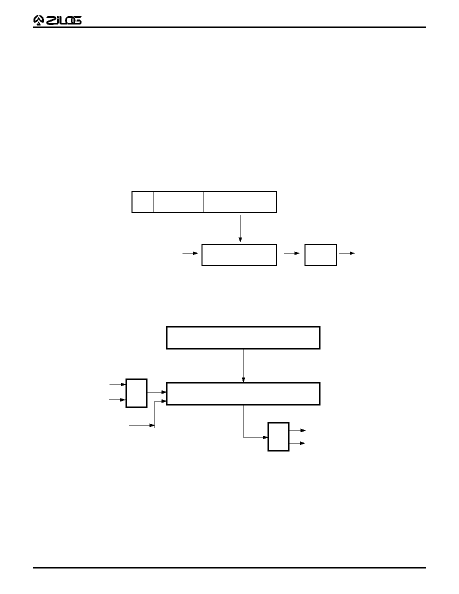
FUNCTIONAL DESCRIPTION
Analog to Digital Converter (ADC)
The ADC is an 8-bit half flash converter that uses two
reference resistor ladders for its upper 4 bits (Most
Significant Bits) and lower 4 bits (Least Significant Bits)
conversion. Two reference voltage pins, VA (High) and VA
(Low), are provided for external reference voltage supplies.
During the sampling period from one of the four channel
inputs, the converter is also being auto-zeroed before
starting the conversion. The conversion time is dependent
on the external clock frequency and the selection of the
prescaler value for the internal ADC clock source. The
minimum conversion time is 2.0
µ
s. (See Figure 9, ADC
Architecture.)
The ADC control register is Bank 13/Ext 0. A conversion
can be initiated in one of four ways: by writing to the
A/D control register, INT1 input pin, Timer 2 or Timer 0
equal 0. These four are programmable selectable. There
are four modes of operation that can be selected: one
channel converted four times with the results written to
each Result register, one channel continuously converted
and one Result channel updated for each conversion, four
channels converted once each and the four results written
to the Result registers, and four channels repeatedly
converted and the Result registers kept updated. The
channel to be converted is programmable and if one of the
four-channel modes is selected then the programmed
channel will be the first channel converted and the other
three will be in sequence following with wraparound from
Channel 3 to Channel 0.
The start commands are implemented in such a way as to
begin a conversion at any time, if a conversion is in
progress and a new start command is received, then the
conversion in progress will be aborted and a new conversion
will be initiated. This allows the programmed values to be
changed without affecting a conversion-in-progress. The
new values will take effect only after a new start command
is received.
The clock prescaler can be programmed to derive a
minimum 2
µ
s conversion time for clock inputs from 4 MHz
to 20 MHz. For example, with a 20 MHz crystal clock the
prescaler should be programmed for divide by 40, which
then gives a 2
µ
s conversion rate.
The ADC can generate an Interrupt after either the first or
fourth conversion is complete depending on the
programmable selection.
The ADC can be disabled (for low power) or enabled by a
Control Register bit.
Though the ADC will function for a smaller input voltage
and voltage reference, the noise and offsets remain constant
during the specified electrical range. The errors of the
converter will increase and the conversion time may also
take slightly longer due to smaller input signals.

19
Z89323/373/393
16-B
IT
D
IGITAL
S
IGNAL
P
ROCESSORS
P R E L I M I N A R Y
DS95DSP0101 Q4/95
Flash
A/D
Converter
Sample
and
Hold
Integrated
Logic
4-Channel
Multiplexer
A/D
Channel
Register
A/D
Controller
Register
4x8
Result
Register
A/D
Prescaler
Start
Converter
INT0
Timer
Internal
Bus
AGND
VREF
Dual
Scan
Channel Select
Figure 9. ADC Architecture

Z89323/373/393
16-B
IT
D
IGITAL
S
IGNAL
P
ROCESSORS
20
P R E L I M I N A R Y
DS95DSP0101 Q4/95
FUNCTIONAL DESCRIPTION
(Continued)
Figure 10. ADCTL Register (Low Byte)
Prescaler Values (bits 7, 6, 5)
Prescaler
D2
D1
D0
(Crystal divided by)
0
0
0
8
0
0
1
1 6
0
1
0
2 4
0
1
1
3 2
1
0
0
4 0
1
0
1
4 8
1
1
0
5 6
1
1
1
6 4
Note:
The ADC is currently being characterized. Converter errors are estimated
to increase to 2 LSBs (Integral non-linearity), 1 LSB (Differential non-
linearity) and 10 mV (Zero error at 25
∞
C) if the voltage swing on the
reference ladder is decreased to ≠3V.
Modes (bits 4, 3)
QUAD
SCAN
0
0
Convert selected channel 4 times
then stop.
0
1
Convert selected channel then stop.
1
0
Convert 4 channels then stop.
1
1
Convert 4 channels continuously.
Channel Select (bits 2, 1, 0)
CSEL2
CSEL1
CSEL0
Channel
0
0
0
0
0
0
1
1
0
1
0
2
0
1
1
3
D7
D6
D5
D4
D3
D2
D1
D0
CSEL0
CSEL1
CSEL2
Bank 13/Ext 0 (low byte)
SCAN
QUAD
D0
D1
D2
ADST0
ADST1
D15 D14 D13 D12 D11 D10 D9
D8
ADIE
Reserved
Bank 13/Ext 0 (high byte)
ADE
ADCINT
ADIT
Figure 11. ADCTL Register (High Byte)
ADE
(bit 15). A 0 disables any A/D conversions or
access≠ing any ADC registers except writing to ADE bit. A
1 Enables all ADC accesses.
Reserved
(bits 14, 13). Reserved for future use.
ADCINT
(bit 12). This is the ADC Interrupt bit and is Read
Only. The ADCINT will be reset any time this register is
written.
ADIT
(bit 11). This bit selects when to set the ADC Interrupt
if ADIE=1. A value of 0 sets the Interrupt after the first A/D
conversion is complete. A value of 1 sets the Interrupt after
the fourth A/D conversion is complete.
ADIE
(bit 10). This is the ADC Interrupt Enable. A value of
0 disables setting the ADC Interrupt. A value of 1 enables
setting the ADC Interrupt.

21
Z89323/373/393
16-B
IT
D
IGITAL
S
IGNAL
P
ROCESSORS
P R E L I M I N A R Y
DS95DSP0101 Q4/95
START (bits 9, 8)
ADST1
ADST0
Mode
0
0
Conversion starts when
this register is written.
0
1
Conversion starts on a
rising edge INT1 input pin.
1
0
Conversion starts when
Timer 2 times out.
1
1
Conversion starts when
Timer 0 times out.
There are four ADC result registers. For their location in the
different banks, see EXT Register Assignments.
Figure 12 shows the input circuit of the ADC. When
conversion starts, the analog input voltage from one of the
eight channel inputs is connected to the MSB and LSB
flash converter inputs as shown in the Input Impedance
CKT diagram. This effectively shunts 31 parallel internal
resistance of the analog switches and simultaneously
charges 31 parallel 0.5 pF capacitors, which is equivalent
to seeing a 400 Ohms input impedance in parallel with a
16 pF capacitor. Other input stray capacitance adds about
10 pF to the input load. For input source, resistances up to
2 kOhms can be used under normal operating conditions
without any degradation of the input settling time. For
larger input source resistance longer conversion cycle
time may be required to compensate the input settling time
factor.
CMOS Switch
on Resistance
2 - 5 k
C Parasitic
R Source
V Ref
C .5 pF
V Ref
C .5 pF
V Ref
C .5 pF
31 CMOS Digital
Comparators
Figure 12. Input Impedance of ADC
Z89323/373/393
16-B
IT
D
IGITAL
S
IGNAL
P
ROCESSORS
22
P R E L I M I N A R Y
DS95DSP0101 Q4/95
FUNCTIONAL DESCRIPTION
(Continued)
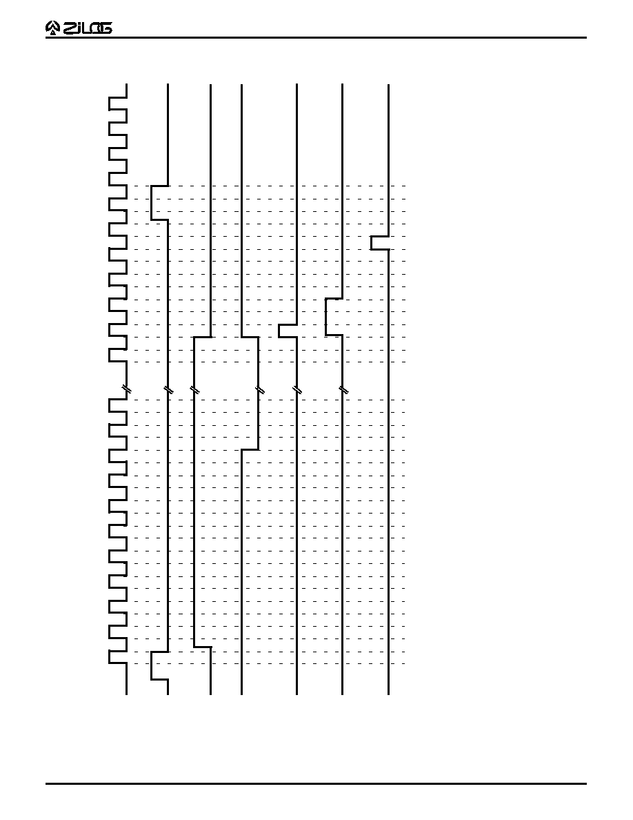
Figure 13. ADC Timing Diagram
SCLK
12
34567
8
9
1
0
1
1
2
6
2
7
2
8
2
9
3
0
3
1
3
2
INT0
CHAN MUX
Input Sample
A/D Result
DSP
INT
DSP
W
rite to
ADC
CTL
REG
Note: 1. SCLK = 20 MHz
1
23
Z89323/373/393
16-B
IT
D
IGITAL
S
IGNAL
P
ROCESSORS
P R E L I M I N A R Y
DS95DSP0101 Q4/95
TIMER/COUNTERS
The Z89323/373/393 has two 16-bit Timer/Counters that
can be independently configured to operate in various
modes. Each is implemented as a 16-bit Load Register
(TMLR) and a 16-bit down counter (TMR). Timer/Counter
inputs can be selected from among UI0 or UI1 pins and
outputs from among UO0 or UO1 pins. The Timer/Counter
clock is a scaled version of system clock. Each counter has
an 8-bit clock prescaler with divide count controlled by the
16-bit Prescaler Load Register (TPLR). The clock rates of
the two timer/counters are independent of each other.
External input events occur optionally on the rising edge,
the falling edge, or both rising and falling edges of the
input. Output actions on external pins can be programmed
to occur with either polarity. The Timer/Counter operational
modes are selected through the 16-bit Control Register
(TCTL). This register defines the operational modes of its
companion Timer (Figure 14).
Each Timer contains a set of five 16-bit Registers. The Ext
Register Assignment specifies the location of each Timer
Registers. All accesses to Timer Registers occur with zero
Wait States.
15
13 12 11
8
7
4
3
0
Test
INP
SEL
MODE
CE
6
5
1
INP
EVENT
OUT
SEL
OUT
INV
14
2
Count Enable
Input Select
Input Event
Output Select
Output Invert
Timer Mode
Reserved
Test Mode
Figure 14. TCTL Register

Z89323/373/393
16-B
IT
D
IGITAL
S
IGNAL
P
ROCESSORS
24
P R E L I M I N A R Y
DS95DSP0101 Q4/95
TIMER/COUNTERS
(Continued)
Timer Modes
The Timer modes can be categorized as input modes and
output modes. In input modes, the Timer/Counter is used
for input signals only. In output modes, a selected output
pin is driven. If a Timer/Counter is enabled (CE=1) and an
output pin, UO0 or UO1, is selected to be driven, the DSP
Processor's Status Register bits 5 or 6 does not affect the
state of that pin.
Output Modes
MODE 0.
The Timer/Counter is configured to generate a
continuous square wave of 50% duty cycle. Writing a new
value to the TMLR Register takes effect at the end of
current cycle unless TMR is written.
MODE 1.
The Timer/Counter is configured to generate a
single pulse of programmable duration. The asserted state
may be either logic high or logic low. Retriggering the one-
shot before the end of the pulse causes it to continue for the
new duration.
MODE 2.
The Timer/Counter is configured to generate a
pulse-width modulated repeating waveform. The duty cycle
ranges from 0≠100% (0/256 to 255/256) of a cycle in steps
of 1/256 of a cycle. The asserted state of the waveform may
be either logic high or logic low. Writing a new pulse-width
value to the TMLR Register takes effect at the end of
current cycle unless TMR is written.
MODE 3.
The Timer/Counter is configured to generate a
pulse-width modulated repeating waveform. The duty cycle
ranges from 0≠100% (0/65,536 to 65,535/65,536) of a
cycle in steps of 1/65,536 of a cycle. The asserted state of
the waveform may be either logic high or logic low. Writing
a new pulse-width value to the TMLR Register takes effect
at the end of current cycle unless TMR is written.
MODE 4.
The Timer/Counter is configured to generate a
series of pulses ranging from 0 to 65,535. The pulses are
actually the Timer Clock (TMCLK), which is gated to the
output until the counter under flows.
MODE 5.
The Timer/Counter is configured to generate an
output pulse that is asserted under program control, and
de-asserted when a programmable number of input edges
(up to 65,535) have been counted on an input pin (UI0 or
UI1). Assertion may be either logic high or logic low.
MODE 6.
The Timer/Counter is configured to generate a
Hardware Reset on time-out unless retriggered by software.
MODE 7.
The Timer/Counter is configured to generate a
Hardware Reset on time-out unless retriggered by an
event on one of the input pins UI0 or UI1.
Input Modes
The input modes use one of the input pins UI0 or UI1. The
signals on these pins are synchronized with the internal
Timer Clock, TMCLK, before being applied to the Timer.
The input signal frequency must be no higher than 1/4th of
TMCLK frequency.
MODE 8.
The Timer/Counter is configured to measure the
time for which its input is asserted.
MODE 9.
The Timer/Counter is configured to measure the
period from one rising (falling) edge to the next rising
(falling) edge on the input.
MODE 10.
The Timer/Counter is configured to count the
number of input edges (up to 65,535). Input edges may be
selected as rising or falling or both.
MODE 11.
The Timer/Counter is configured to count the
number of input edges (up to 65,535) in a time window set
by the second timer. Edges are counted until the second
timer under flows. Input edges may be selected as rising
or falling or both.
25
Z89323/373/393
16-B
IT
D
IGITAL
S
IGNAL
P
ROCESSORS
P R E L I M I N A R Y
DS95DSP0101 Q4/95
15 14 13 12
11
10
9
8
7
6
5
4
3
2
1
0
Timer Control Register (TCTL)
Timer/Counter
0 Timer/Counter disabled (default)
1 Timer/Counter enabled
Input Select
00 Inputs have no effect
01 Reserved
10 UI0 Pin
11 UI1 Pin
Input Event
00 Low Level or Falling Edge
01 High Level or Rising Edge
10 Both Rising and Falling Edges
11 Reserved
Output Select
00 Outputs Unaffected
01 Reserved
10 Drive UO0 Pin
11 Drive UO1 Pin
Output Invert
0 Output asserted High on Timeout
1 Output asserted Low on Timeout
Timer Mode
Timer Output Modes
0000 Square Wave Mode 0
0001 One-Shot Mode 1
0010 PWM short (8-bit) Mode 2
0011 PWM long (16-bit) Mode 3
0100 Pulse Count Output Mode 4
0101 Triggered Count Mode 5
0110 S/W Watch-Dog Mode Mode 6
0111 H/W Watch-Dog Mode Mode 7
Timer Input Modes
1000 Gated Count Mode 8
1001 Period Mode 9
1010 Pulse Count Mode 10
1011 Gated Pulse Count Mode 11
Reserved
Test Mode*
0 Normal Operation
1 Factory Test Mode
*Note: The user should always
program this bit to be 0.
Bank 13/EXT1 (Timer0) or Bank 14/EXT1 (Timer1)
Figure 15. Register Bit Fields

Z89323/373/393
16-B
IT
D
IGITAL
S
IGNAL
P
ROCESSORS
26
P R E L I M I N A R Y
DS95DSP0101 Q4/95
TIMER/COUNTERS
(Continued)
Timer Load Register (TMLR)
This 16-bit Register holds a value that is reloaded into timer
upon timer under flow.
Timer Register (TMR)
TMR is a 16-bit down counter that holds the current Timer/
Counter value. It can be read as any ordinary register.
However, writing to TMR is different than writing to an
ordinary register. A write to TMR Register causes the
contents of TMLR Register to be written into it, causing the
Timer to be retriggered. Any data on DSP's Memory Data
(MD) Bus is ignored during a write to TMR.
Timer Reload Value
15
0
Timer Prescaler Load Register (TPLR)
The 16-bit TPLR Register holds the prescaler reload value
in its lower 8 bits. Bit 15 is the Timer's Interrupt Pending bit.
When set, it signifies an interrupt event in its companion
timer. The IP bit can only be set by the Timer. It can be
cleared only by software when it writes a value to this
register with a "1" in bit position 15; a "0" in bit position 15
will have no effect on the state of IP bit. Bits [14:8] must
always be written with 0s for future compatibility.
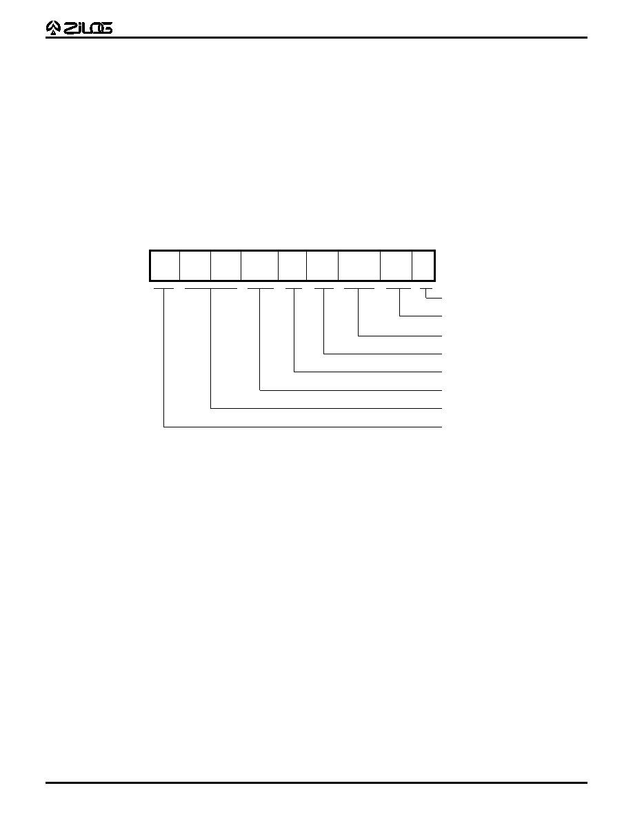
Timer Register
15
0
Timer Prescale Register (TPR)
TPR is an 8-bit down counter that holds the current Prescaler
count value. It can be read as any ordinary register.
However, writing to TPR is different than writing to an
ordinary register. A write to TPR Register causes the lower
8-bit contents of TPLR Register to be written into it, causing
the Prescaler to be retriggered. Any data on DSP's Memory
Data (MD) Bus is ignored during a write to TPR.
7
TPR
8-Bit Counter
0
Prescaler
Reload Value
14
8 7
Zeros
15
0
Test
27
Z89323/373/393
16-B
IT
D
IGITAL
S
IGNAL
P
ROCESSORS
P R E L I M I N A R Y
DS95DSP0101 Q4/95
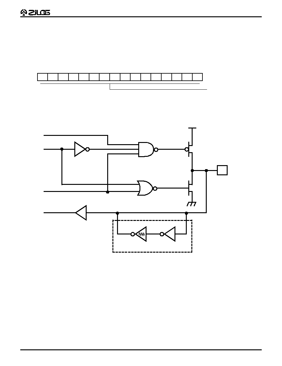
Prescaler Operation
The Timer/Counter Clock (TMCLK) is generated by the
output of the prescaler. The Prescaler is an 8-bit down
counter, TPR, followed by a divide-by-two flip-flop that
generates a 50 percent duty cycle output clock TMCLK.
The Prescaler's input clock is the system clock, CLKIN,
divided by two. Thus, the maximum prescaler output
frequency is 1/4 of the system clock frequency.
Once the prescaler counter is loaded, it decrements at its
clocked frequency and generates an output to the divide-
by-two flip-flop. When the count reaches 0, the counter is
reloaded from the lower 8 bits of TPLR Register.
The 8-bit prescaler counter is loaded with value in TPLR
Register field [7:0] in one of three ways:
1. When 8-bit prescaler counter, TPR,
decrements to zero.
2. By writing to TPR Register.
3. When companion Timer/Counter TMR is reloaded
upon under flow from its TMLR Register, or
retriggered by writing directly to TMR Register.
Figure 16. Prescaler Block Diagram
15
0
TMLR Register
UIO
M
U
X
TMCLK
UI1
TMR Register
16-Bit Counter
15
0
U00
S
E
L
U01
Figure 17. Counter/Timer Block Diagram
15
0
Prescaler
Reload Value
14
8
7
IP
Zeros
TPLR
Register
TPR
8-Bit Counter
Clock
(System Clock)
DIV
by 2
TMCLK

Z89323/373/393
16-B
IT
D
IGITAL
S
IGNAL
P
ROCESSORS
28
P R E L I M I N A R Y
DS95DSP0101 Q4/95
TIMER/COUNTERS
(Continued)
16-Bit General-Purpose Timer/Counter T2
The 16-bit timer/counter is available for general-purpose
use. When the counter counts down to the zero state, the
timer 2 load register loads into timer 2, and if timer 2
interrupt is enabled, an interrupt is received. The counting
operation of the counter can be disabled. The timer/
counter clock source can be selected to be system clock/
2 or UI2.
The counter is defaulted to the Enable state. If the system
designer does not choose to use the timer, the counter can
be disabled.
Figure 18. Timer/Counter 2 Load Register
I/O Ports
Bank 14/EXT 0
Count Value (Down-Counter)
D15
D14
D13
D12
D11
D10
D9
D8
D7
D6
D5
D4
D3
D2
D1
D0
I/O pin allocation for ports in the different package types is
designed to provide increased flexibility and support for
various modes of operation. The 44-pin package features
the special signals, as well as all packages supporting the
EXT 16-bit bus. In cases where the application does not
require an external EXT bus, these I/O pins can be allocated
to 16-bit general-purpose I/O port (P0), the special signals
port (P1) or additional port (P3). The 80-pin PQFP package
supports up to 40 I/O pins.
Table 9. Various Package I/O Port Allocation
Pin Count
44-Pin
68-Pin
80-Pin
100-Pin
Package
PLCC/PQFP
PLCC
PQFP
PQFP
P0[15:8]
EXT,P0,P1*
EXT,P0
EXT,P0
EXT,P0
P0[7:0]
EXT,P0
EXT,P0
EXT,P0
EXT,P0
P1[7:0]
P1*
P1*
P1*
P2[7:0]
P2[4:0]*
P2*
P2*
P2*
P3[7:0]
P 3
Note:
*
Ports with special signals: Interrupts inputs, Serial Peripheral Interface
(SPI), CLKOUT and Timers inputs and outputs.
(ICE chip)
29
Z89323/373/393
16-B
IT
D
IGITAL
S
IGNAL
P
ROCESSORS
P R E L I M I N A R Y
DS95DSP0101 Q4/95
16-bit Programmable I/O (Port 0)
When the appropriate bit is set in the Port 1 control register,
Port 0 acts as a 16-bit programmable, bidirectional, CMOS-
compatible port. Each of the 16 lines can be independently
programmed as an input or an output, or globally as an
open-drain output. When enabled, Bank 0/Ext 4 acts as the
data I/O register. Bank 15/Ext 0 serves as the Port 0
direction register while Bank 15/Ext 1, has specified bits to
enable Port 0 and determine whether Port 0 is globally
configured as open-drain outputs.
Bank 15/Ext 0 Reg
D15
D14
D13
D12
D11
D10
D9
D8
D7
D6
D5
D4
D3
D2
D1
D0
Port I/O Direction
0 = Output
1 = Input
Figure 19. Port 0 Control Register
OEN
Out
In
Pad
Auto Latch
R
500 kOhms
Open-Drain
Figure 20. Port 0, 1 and 2 Configuration
Z89323/373/393
16-B
IT
D
IGITAL
S
IGNAL
P
ROCESSORS
30
P R E L I M I N A R Y
DS95DSP0101 Q4/95
8-Bit Programmable I/O (Port 1)
When the appropriate bit is set in the Port 1 control register,
Port 1 acts as an 8-bit programmable, bi-directional,
CMOS-compatible port. Each of the eight lines can be
independently programmed as an input or an output or
globally as an open-drain output. When enabled,
Bank0/EXT5 (Least Significant Bit) acts as the data I/O
register. Bank15/EXT1 serves as the Port1 direction control
register. Port 1 can also be programmed to provide special
I/O functions.
Table 10. Port 1 Bit Function Selection
Port.Bit
IF (Condition Explanation)
Then
Else
P1.0
Bank15/Ext1(3)=1 (Enable External Interrupt Source INT2)
INT2
P10
P1.1
Bank15/Ext1(5)=1 (CLKOUT Enable)
CLKOUT
P11
P1.2
Bank15/Ext4(0)=1 (SPI Enable)
SIN
P12
P1.3
Bank15/Ext4(0)=1 (SPI Enable)
SOUT
P13
P1.4
Bank15/Ext4(0)=1 (SPI Enable)
S S
P14
P1.5
Bank15/Ext4(0)=1 (SPI Enable)
SK
P15
P1.6
Bank13/Ext1(2-1)=10 or Bank14/Ext1(2-1)=10 (UI0 Enable)
UI0
P16
P1.7
Bank13/Ext1(2-1)=11 or Bank14/Ext1(2-1)=11 (UI0 Enable)
UI1
P17
D7
D6
D5
D4
D3
D2
D1
D0
D15
D14
D13
D12
D11
D10
D9
D8
Bank 15/Ext 1 Reg
1 : Enable External Interrupt Source INT2
0 : Disable External Interrupt Source (default)
Pins P0 15-0 Port Allocation
000 : Ext 15-0 (default)
001 : P0 15-8 <= P1 7-0,
P0 7-0 <= Ext 7-0
010 : Reserved
011 : P0 15-8 <= P0 15-8,
P0 7-0 <= Ext 7-0
100 : P0 15-0
101 : P0 15-8 <= P1 7-0
P0 7-0 <= P0 7-0
110 : Reserved
111 : Reserved
1 : Enable External Interrupt Source INT1
0 : Disable External Interrupt Source (default)
1 : CLKOUT Enabled (P11)
0 : CLKOUT Disabled (default)
1 : Port 1 Outputs Open-Drain
0 : Port 1 Outputs Push-Pull (default)
1 : Port 0 Outputs Open-Drain
0 : Port 0 Outputs Push-Pull (default)
Port 1 I/O Directions
1 : Output
0 : Input (default)
Figure 21. Bank15/EXT1 Register
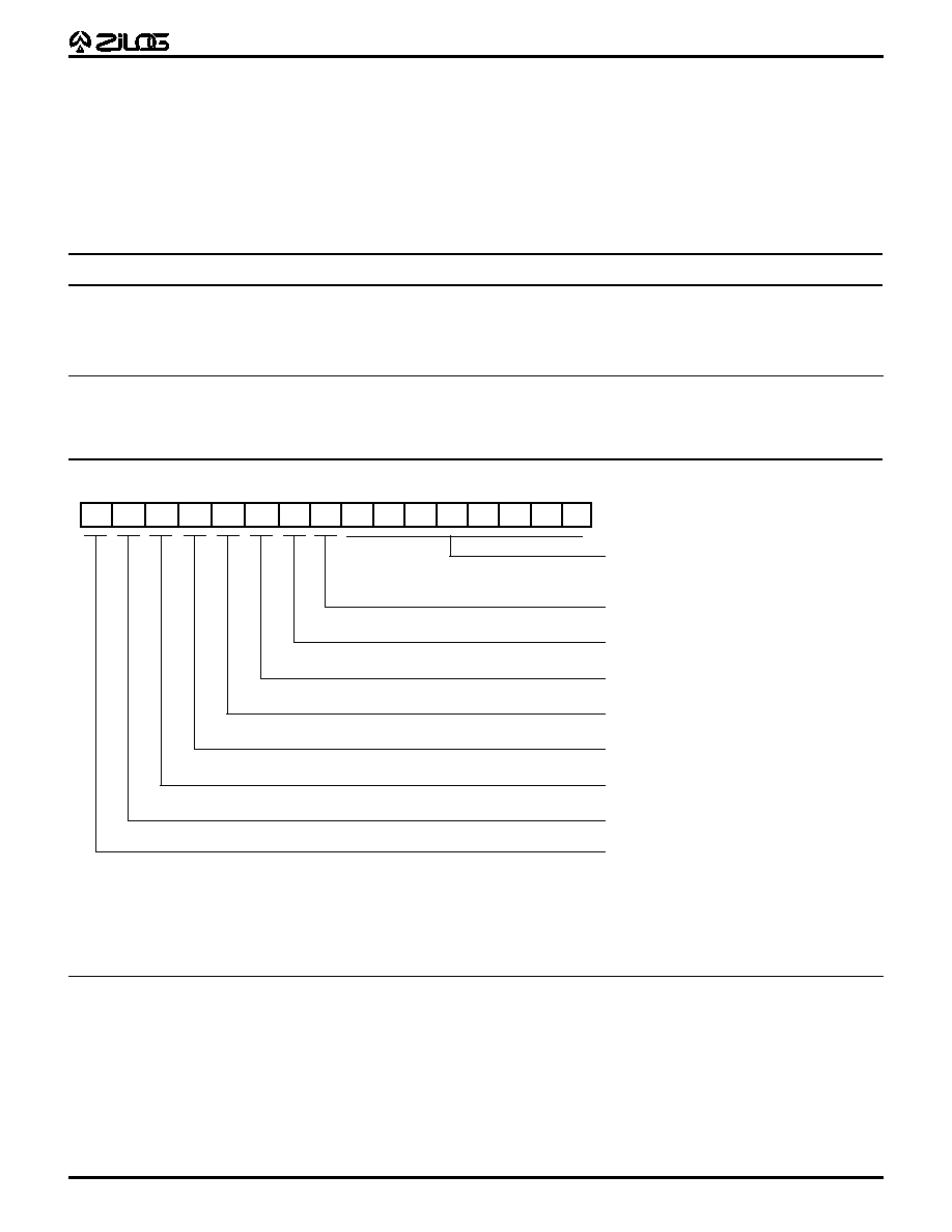
31
Z89323/373/393
16-B
IT
D
IGITAL
S
IGNAL
P
ROCESSORS
P R E L I M I N A R Y
DS95DSP0101 Q4/95
8-Bit Programmable I/O (Port 2)
Port 2 is an 8-bit programmable, bidirectional, CMOS-
compatible port. Each of the eight lines can be
independently programmed as an input or an output or
globally as an open-drain output. Port 2 can also be
programmed to provide special I/O functions. When Port 2
acts as programmable I/O, Bank0/EXT5 (MSB) acts as the
data I/O register. Bank15/EXT2 serves as Port 2 control
register.
Table 11. Port 2 Bit Function Selection
Port.Bit
IF (Condition Explanation)
Then
Else
P2.0
Bank15/Ext2(9)=1 (Enable External Interrupt Source INT0)
INT0
P20
P2.1
Bank15/Ext1(4)=1 (Enable External Interrupt Source INT1)
INT1
P21
P2.2
Bank13/Ext1(6-5)=10 or Bank14/Ext1(6-5)=10 (UO0 Enable)
UO0
P22
P2.3
Bank13/Ext1(6-5)=11 or Bank14/Ext1(6-5)=11 (UO0 Enable)
UO1
P23
P2.4
Bank15/Ext2(14)=1 (UO2 Enable)
UO2
P24
P2.5
Bank15/Ext2(13)=1 (Timer2 Clock is UI2)
UI2
P25
P2.6
P26
P26
P2.7
P27
P27
D7
D6
D5
D4
D3
D2
D1
D0
D15
D14
D13
D12
D11
D10
D9
D8
Bank 15/Ext 2 Reg
1 : Enable Port 3
0 : Disable Port 3 (default)
Port 2 I/O Directions
1 : Output
0 : Input (default)
1 : Enable External Interrupt Source INT0
0 : Disable External Interrupt Source INT0 (default)
1 : Port 2 Outputs Open-Drain
0 : Port 2 Outputs Push-Pull (default)
1 : Enable Timer 2
0 : Disable Timer 2 (default)
1 : Enable Timer 2 Counting
0 : Disable Timer 2 Counting (default)
1 : Timer 2 Clock is UI2
0 : Timer 2 Clock is System Clock/2 (default)
1 : UO2 Enabled (P24)
0 : UO2 Disabled (default)
Timer2 Test Mode*
0 : Normal Operation (default)
1 : Factory Test Mode
*Note:
The user should always program this bit to be 0.
Figure 22. Bank15/EXT2 Register
8-Bit Programmable I/O (Port 3)
Port 3 is an additional I/O port featured only in the 80-pin
PQFP package. P3[3:0] are inputs and P3[7:4] are outputs.
The purpose of this additional port is to serve applications
that need more than 32 I/O pins. Port 3 enables the
user to support up to 40 I/O pins. Port 3 is not
supported in the 100-pin ICE chip PQFP package,
therefore this port is not supported in the Z893x3
emulator, and use of this port is not
recommended in cases when the other I/O ports
can support the I/O requirements.
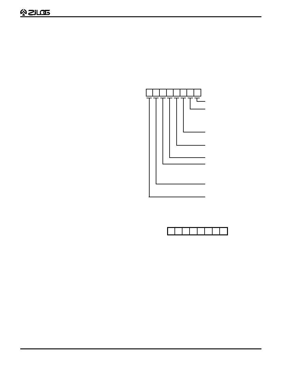
Z89323/373/393
16-B
IT
D
IGITAL
S
IGNAL
P
ROCESSORS
32
P R E L I M I N A R Y
DS95DSP0101 Q4/95
D7
D6
D5
D4
D3
D2
D1
D0
Bank 0/Ext 3 (LSB) Reg
Figure 24. SPI TXRXDATA Register
D7
D6
D5
D4
D3
D2
D1
D0
SPI Enable
1 Enable
2 Disable
Bank15/Ext4 (LSB) Reg
Receive Character Overrun (Slave)
Clock Frequency (Master)
0 0 Divide-by-2
0 1 Divide-by-4
1 0 Divide-by-8
1 1 Divide-by-16
DOP (Slave)
0 Enable SOUT as Output
1 Tri-State SOUT
SSP = SS Polarity (Master)
0 = SS Active Low (default)
1 = SS Active High
Received Character Available
CLKP
0 is Transmit on Falling
Receive Data on Rising Edge
1 is Transmit on Rising
Receive Data on Falling Edge
SPI Clock Source Select (Master)
0 is Internal Clock
1 is Timer 0
1 Master 0 Slave
Figure 23. SPI Control Register (SCON)
slave's SPI Shift Register, through the SIN pin, which has
the same address as the RxBUF Register. After a byte of
data has been received by the SPI Shift Register a Receive
Character Available SPI interrupt and flag is generated.
The next byte of data may be received at this time, but the
RxBUF Register must be cleared, or a Receive Character
Overrun (RxCharOverrun) flag is set in the SCON Register
and the data in the RxBUF Register is overwritten.
Serial Peripheral Interface
Serial Peripheral Interface
(SPI). The Z893X3 incorporates
a serial peripheral interface for communication with other
microcontrollers and peripherals. The SPI includes features
such as Master/Slave selection. The SPI consists of two
registers; SPI Control Register (SCON), SPI Receive/Buffer
Register (RxBUF), and SPI Shift Register (Figure 23).
Note:
The SPI shift register and Receive/Buffer register are one
in the same and are shown in Figure 41. SCON is located
in bank 15/Ext4 (LSB). This register is a read/write register
that controls; Master/Slave selection, SS polarity, clock
source and phase selection, and error flag. Bit 0 enables/
disables the SPI with the default being SPI disabled. A 1 in
this location enables the SPI, and a 0 disables the SPI.
Bits 1 and 2 of the SCON register in Master Mode selects
the clock rate. The user may choose whether internal clock
is divide by 2, 4, 8, or 16. In Slave Mode, Bit 1 of this register
flags the user if an overrun of the RxBUF Register has
occurred.
The RxCharOverrun flag can only be reset by writing a 0 to
this bit. In slave mode, bit 2 of the Control Register can
disable the data-out I/O function. If a 1 is written to this bit,
the data-out pin is tri-stated. If a 0 is written to this bit, the
SPI will shift out one bit for each bit received. Bit 3 of the
SCON Register is the SS polarity bit. A 0 selects active Low
(default) polarity on SS, and a 1 selects active High. Bit 4
signals that a receive character is available in the RxBUF
Register. If the associated interrupt enable bit is enabled,
an interrupt is generated. Bit 5 controls the clock phase of
the SPI. A 1 in Bit 5 allows for receiving data on the clock's
falling edge and transmitting data on the clock's rising
edge. A 0 allows receiving data on the clock's rising edge
and transmitting on the clock's falling edge.
The SPI clock source is defined in bit 6 for Master mode.
A 1 uses Timer0 output for the SPI clock, and a 0 uses a
division of the internal system clock for clocking the SPI. Bit
7 determines whether the SPI is used as a Master or a
Slave. A 1 puts the SPI into Master mode and a 0 puts the
SPI into Slave mode.
SPI Operation.
The SPI can be used in one of two modes;
either as system slave, or a system master. In the slave
mode, data transfer starts when the slave select
(SLAVESEL) pin goes Low. Data is transferred into the

33
Z89323/373/393
16-B
IT
D
IGITAL
S
IGNAL
P
ROCESSORS
P R E L I M I N A R Y
DS95DSP0101 Q4/95
When the communication between the master and slave is
complete, the SS goes High. Unless disconnected, for
every bit that is transferred into the slave through the SIN
pin, a bit is transferred out through the SOUT pin on the
opposite clock edge. During slave operation, the SPI clock
pin (SK) is an input (Figure 25). In master mode, the DSP
must first activate a SS through one of it's I/O ports. Next,
data is transferred through the master's SOUT pin one bit
per master clock cycle. Loading data into the shift register
initiates the transfer. In master mode, the master's clock
drives the slave's clock. At the conclusion of a transfer, a
Receive Character Available SPI interrupt and flag is
generated. Before data is transferred through the SOUT
pin, the SPI Enable bit in the SCON Register must be
enabled. The MSB bit 7 is shifted out first.
SPI Clock.
The SPI clock can be driven from three sources;
with T0, a division of the internal system clock, or an
external master when in slave mode. Bit D6 of the SCON
Register controls what source drives the SPI clock. Divided
by 2, 4, 8, or 16 can be chosen as the scaler with bits D2,
D1 in master mode.
Receive Character Available and Overrun.
When a
complete data stream is received an interrupt is generated
and the RxCharAvail bit in the SCON Register is set. The
SPI interrupt can be enabled or disabled (default) in the
Interrupt Allocation Register (Bank 15/Ext 6). The
RxCharAvail bit is available for interrupt polling purposes
and is reset when the RxBUF Register is read. RxCharAvail
is generated in both master and slave modes. While in
slave mode, if the RxBUF is not read before the next data
stream is received and loaded into the RxBUF Register,
Receive Character Overrun (RxCharOverrun) occurs. Since
there is no need for clock control in slave mode, bit D1 in
the SPI Control Register is used to log any RxCharOverrun.
SK
3
4
2
1
5
SS
SOUT
SIN
(Input/Output
Input
(Active Low)
Figure 25. SPI Timing

Z89323/373/393
16-B
IT
D
IGITAL
S
IGNAL
P
ROCESSORS
34
P R E L I M I N A R Y
DS95DSP0101 Q4/95
CLOCK Circuits
The clock generator includes Phase-Locked Loop (PLL)
circuit to enable use of low frequency crystal. The benefits
of using low frequency crystal are low system cost, low
power consumption and low EMI. The PLL circuit can be
bypass (s/w controlled).
The clock generated by the PLL circuit (VCO clock) is
programmable and controlled by the PLL Divider register.
DSP (System) clock source is programmable and can be
one of the 4 options: VCO clock, VCO clock divided by 2,
VCO clock divided by 4 or twice the crystal frequency.
Whenever the PLL circuit is switched from Stop VCO to
Enable VCO, a software delay of 10 msec must be used
before switching the system clock from the oscillator to the
PLL, in order to give the PLL time to be stable.
00
01
10
11
MUX
:2
:2
VCO
8-Bit
Divider
Phase
Detector
:2
STOP_VCO
0
1
MUX
Clock Source
PLL Divider
BYPASS_PLL
STOP_OSC
Bank4 / Ext5
0
[15-8]
1
[4-3]
2
LPF
32 kHz
System
Clock
Off-Chip
On-Chip
Figure 26. PLL Functional Block Diagram
Table 12. CLOCK Modes
STOP_OSC
STOP_VCO
BYPASS_PLL
Mode
0
0
0
0) Normal - High frequency clock
0
0
1
1) 32 Khz - VCO running (fast switching time)**
0
1
0
2) STOP CLOCK - Oscillator running
0
1
1
3) 32 Khz
1
1
0
4) STOP CLOCK
1
1
1
5) EXTERNAL CLOCK source *
Notes:
*
In this clock mode, it is possible to use external clock source instead
of the internal oscillator source.
**
Default (power-up) mode of operation.
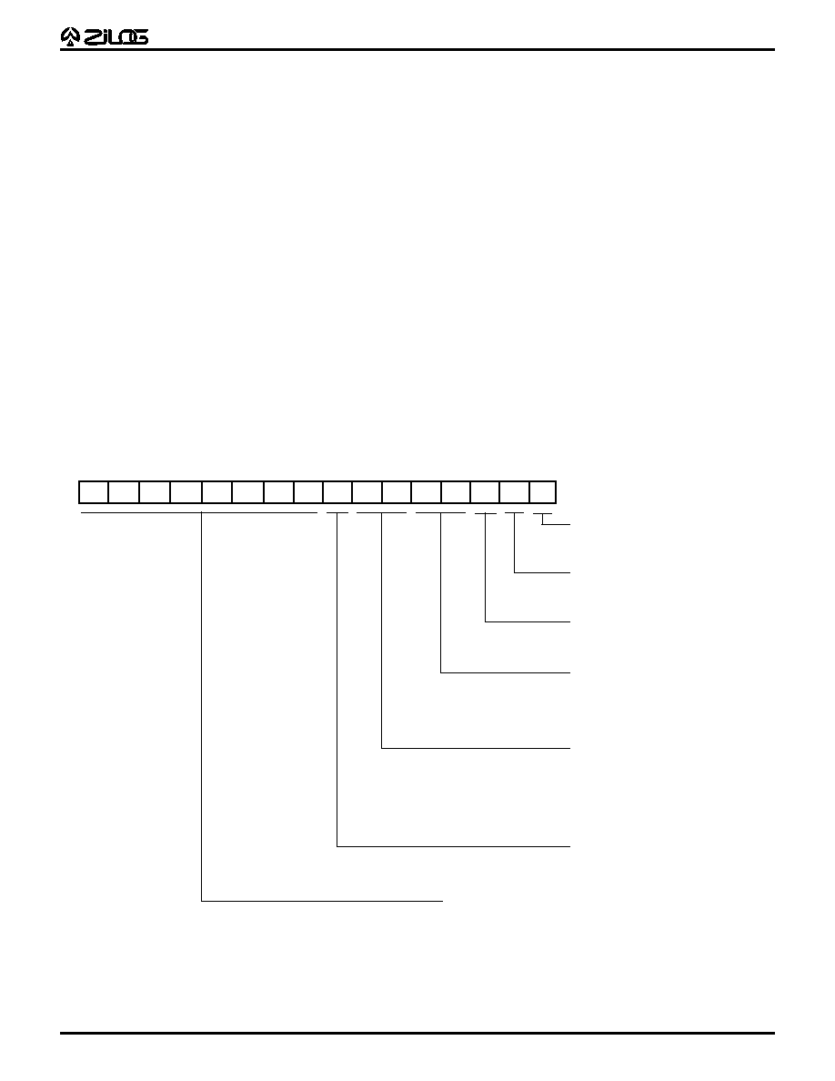
35
Z89323/373/393
16-B
IT
D
IGITAL
S
IGNAL
P
ROCESSORS
P R E L I M I N A R Y
DS95DSP0101 Q4/95
Power Down
The Z893X3 supports different levels of power-down modes
to minimize device power consumption. The lowest power
consumption is at STOP Clock Mode when the Oscillator
is turned off (clock modes 2 and 4 when there is no external
clock.) The highest power consumption is when the Z893X3
in Normal mode (Clock Mode 0) and there is medium
power consumption mode .The SLOW Clock Mode is when
the DSP is running with 32 kHz clock (Crystal Clock Modes
1 and 3) and disabling all the peripherals which are not
needed in this mode.
Slow Mode
The SLOW mode reduce the chip power consumption by
using the 32 kHz clock (Clock Mode 3) of the crystal as a
DSP clock and disabling in software all the unnecessary
peripherals.
Clock Mode 1 also uses the 32 kHz clock, but in this mode
the VCO is still running to enable fast switching (wake up)
to the high frequency.
Stop Mode
The STOP mode provides the lowest possible device
standby current. In this mode of operation the on chip
oscillator and internal system clock are turned off.
In Clock Mode 2 the Oscillator is running while the system
clock is turned off to enable fast switching (wake up) to the
high frequency.
STOP mode is exited when the recovery source as defined
in Bank4/EXT5[6:5] is toggled to the recovery defined
level. In case of Clock Mode 2 the program resumes
operation starting from the next instruction after the stop
instruction. In case of Clock Mode 4, the program resumes
operation starting from the reset vector address after
executing operations similar to the Power-On Reset
sequence of operations.
D7
D6
D5
D4
D3
D2
D1
D0
D15
D14
D13
D12
D11
D10
D9
D8
Bank 15/Ext 5 Reg
STOP Recovery Level
0 : Low (Default setting after reset.)
1 : High
STOP_VCO
0 : VCO Running
1 : Stop VCO
BYPASS_PLL
0 : Clock Source is VCO
1 : Clock Source is Oscillator
DSP (System) Clock Source
00 : VCO Clock
01 : VCO Clock Divided by 2
10 : VCO Clock Divided by 4
11 : Twice the Crystal Frequency
Recovery Source
00 : POR (Power-On Reset) or
Port 2, Bit 0 (INT0)
01 : POR or Port 1, Bit 4 (SS)
10 : POR or Port 1, Bit 6 (UI0)
11 : POR or Port 2, Bit 0 or
Port 1, Bit 4 or Port 1, Bit 6
Programmable PLL Divider Register
VCO Frequency = Bits 15-8 * 8 * Crystal Frequency (32 kHz)
39 (9.984 MHz) < Bits 15-8 < 158 (40.448 MHz)
STOP_OSC
0 : Oscillator Running
1 : Stop Oscillator
Figure 27. PLL Register

Z89323/373/393
16-B
IT
D
IGITAL
S
IGNAL
P
ROCESSORS
36
P R E L I M I N A R Y
DS95DSP0101 Q4/95
Interrupt Controller
There are eight different interrupt sources (when all of them
are enabled). Bits [3:0] of the Interrupt Allocation Register
defines which interrupt source will have the highest priority
and will be allocated into IINT0 (Internal INT0). Bits[7:0] of
the Interrupt Allocation Register defines which interrupt
source will have the second highest priority and will be
allocated into IINT1 (Internal INT1). Bits[15:8] are enable
bits for specific interrupt sources. All the enabled interrupts
which are not already allocated into IINT0 or IINT1 are
allocated into IINT2. When interrupt happen on IINT2 then
IINT2 interrupt routine is reading the Interrupt Status Register
(EXT7 in all the Banks) to determine which interrupt occurred
and decides on the relative priority. The Interrupt Status
Register can be used for polling interrupts mode.
IINT0 Source
Note: An Interrupt that is not selected as a source to IINT0, IINT1 or IINT2 is disabled.
D7
D6
D5
D4
D3
D2
D1
D0
D15
D14
D13
D12
D11
D10
D9
D8
Bank 15/Ext 6 Reg
0000 : A/D Finish
0010 : Timer0
0100 : Timer2
0110 : INT1 H/W
1000 ≠ 1111 : IINT0 Disabled
0001 : SPI
0011 : Timer1
0101 : INT0 H/W
0111 : INT2 H/W
IINT1 Source
0000 : A/D Finish
0010 : Timer0
0100 : Timer2
0110 : INT1 H/W
1000 ≠ 1111 : IINT1 Disabled
0001 : SPI
0011 : Timer1
0101 : INT0 H/W
0111 : INT2 H/W
Interrupt
Enable
Interrupt
Disable
IINT2 Interrupt Sources
Bit 8 = A/D Finish
1
Bit 9 = SPI
1
Bit 10 = Timer0
1
Bit 11 = Timer1
1
Bit 12 = Timer2
1
Bit 13 = INT0 H/W 1
Bit 14 = INT1 H/W 1
Bit 15 = INT2 H/W 1
0
0
0
0
0
0
0
0
Figure 28. Interrupt Allocation Register

37
Z89323/373/393
16-B
IT
D
IGITAL
S
IGNAL
P
ROCESSORS
P R E L I M I N A R Y
DS95DSP0101 Q4/95
FUNCTIONAL DESCRIPTION
Instruction Timing.
Most instructions are executed in one
machine cycle. Long immediate instructions and Jump or
Call instructions are executed in two machine cycles. A
multiplication or multiplication/accumulate instruction
requires a single cycle. Specific instruction cycle times are
described in the Condition Code section.
Multiply/Accumulate.
The multiplier can perform a 16-bit
x 16-bit multiply, or multiply accumulate, in one machine
cycle using the Accumulator and/or both the X and Y
inputs. The multiplier produces a 32-bit result, however,
only the 24 most significant bits are saved for the next
instruction or accumulation. For operations on very small
numbers where the least significant bits are important, the
data should first be scaled by eight bits (or the multiplier
and multiplicand by four bits each) to avoid truncation
errors. Note that all inputs to the multiplier should be
fractional two's-complement, 16-bit binary numbers (Figure
29). This puts them in the range [≠1 to 0.9999695], and the
result is in 24 bits so that the range is [≠1 to 0.9999999]. In
addition, if 8000H is loaded into both X and Y registers, the
resulting multiplication is considered an illegal operation
as an overflow would result. Positive one cannot be
represented in fractional notation, and the multiplier will
actually yield the result 8000H x 8000H = 8000H (≠1 x ≠1
= ≠1).
ALU.
The ALU has two input ports, one of which is
connected to the output of the 24-bit Accumulator. The
other input is connected to the 24-bit P-Bus, the upper 16
bits of which are connected to the 16-bit D-Bus. A shifter
between the P-Bus and the ALU input port can shift the
data by three bits right, one bit right, one bit left or no shift
(Figure 30).
Arithmetic Logic Unit (ALU)
24
24
Accumulator (24)
24
* Options:
1 Bit Right
3 Bits Right
No Shift
1 Bit Left
DDATA
MUX
24
16
Mult. (24)
Shift Unit *
24
24
X Register (16)
Y Register (16)
Multiplier
P Register (24)
DDATA
XDATA
16
16
MUX
Shift Unit *
24
24
24
24
* Options:
1 Bit Right
3 Bits Right
No Shift
1 Bit Left
Figure 29. Multiplier Block Diagram
Figure 30. ALU Block Diagram

Z89323/373/393
16-B
IT
D
IGITAL
S
IGNAL
P
ROCESSORS
38
P R E L I M I N A R Y
DS95DSP0101 Q4/95
FUNCTIONAL DESCRIPTION
(Continued)
Hardware Stack.
A six-level hardware stack is connected
to the D-Bus to hold subroutine return addresses or data.
The Call instruction pushes PC+2 onto the stack, and the
RET instruction pops the contents of the stack to the PC.
User Inputs.
The Z89323 has two inputs, UI0 and UI1,
which may be used by Jump and Call instructions. The
Jump or Call tests one of these pins and if appropriate,
jumps to a new location. Otherwise, the instruction behaves
like a NOP. These inputs are also connected to the status
register bits S10 and S11, which may be read by the
appropriate instruction (Figure 8).
User Outputs.
The status register bits S5 and S6 connect
directly to UO0 and UO1 pins and may be written to by the
appropriate instruction.
Note:
The user output value is the
opposite of the status register content.
Interrupts.
The Z89323 has three positive edge-triggered
interrupt inputs serving up to eight interrupt sources. An
interrupt is acknowledged at the end of an instruction
execution. It takes two machine cycles to enter an interrupt
instruction sequence. The PC is pushed onto the stack and
Interrupts are globally disabled. A RET instruction transfers
the contents of the stack to the PC and decrements the
stack pointer by one word. The priority of the interrupts is
IINT0 = highest, IINT2 = lowest.
Note:
The SIEF instruction
globally enables the interrupts. The SIEF instruction must
be used before exiting an interrupt routine since the
interrupts are automatically disabled when entering the
routine. (See Interrupt Controller section for more details.)
Registers.
The Z89323 has 28 physical internal registers,
eight external registers and 15 peripheral control registers.
The EA2-EA0 determines the address of the external
registers. The signals are used to read from or write to the
external registers /DS, WAIT, RD//WR.
I/O Bus.
The processor provides a 16-bit, CMOS-
compatible bus. I/O Control pins provide convenient
communication capabilities with external peripherals, and
single-cycle access is possible. For slower
communications, an on-board hardware wait-state
generator can be used to accommodate timing conflicts.
Three latched I/O address pins are used to access external
registers. Disabling a peripheral allows access to these
addresses for general-purpose use.
Wait-State Generator.
An internal Wait-State generator is
provided to accommodate slow external peripherals. A
single Wait-State can be implemented through a control
register. For additional states, a dedicated pin
(WAIT) can be held High. The WAIT pin is monitored only
during execution of a read or write instruction to external
peripherals (EXT bus).
Analog to Digital Converter.
The Z89323 has a 4-channel,
8-bit half-flash analog to digital converter. Two external
reference voltages are available externally. The ADC
prescales to the system clock and can drive an interrupt at
the end of a conversion. There are four channels of input
with the ADC which can be programmed to convert values
either continuously or on an event (timer or interrupt).
Timer/Counter/PWMs (T0, T1).
Timer0 and Timer1 are
16-bit timer-counters with 8-bit prescalers. They also offer
the option of being used as PWM generators and have
both hardware and software Watch-Dog capabilities. Both
timers are identical and can be externally or internally
clocked and can drive any of the three hardware interrupts.
Timer/Counter (T2).
Timer 2 is a general-purpose 16-bit
timer/counter. It can be externally or internally clocked and
drive either IINT0 and IINT1.
Port 0.
Port 0 is a 16-bit user I/O port. Bits can be
configured as input or output or globally as open-drain
output. When enabled, Port 0 consumes the 16 data lines
used by the EXT bus. Port 0 function and EXT use can be
dynamically changed by enabling and disabling Port 0.
Port 1.
Port 1 is an 8-bit user I/O port. Bits can be
configured as input or output or globally as open-drain
output.
Port 2.
Port 2 has multiple functions. It can be used as an
8-bit user I/O port when the other functions within the port
are not in use. As an I/O port, these bits can be configured
as input or output or globally as open-drain output. Port 2
also supports the SPI, CLKOUT, all three external hardware
interrupt signals and all three timer input and output
signals.
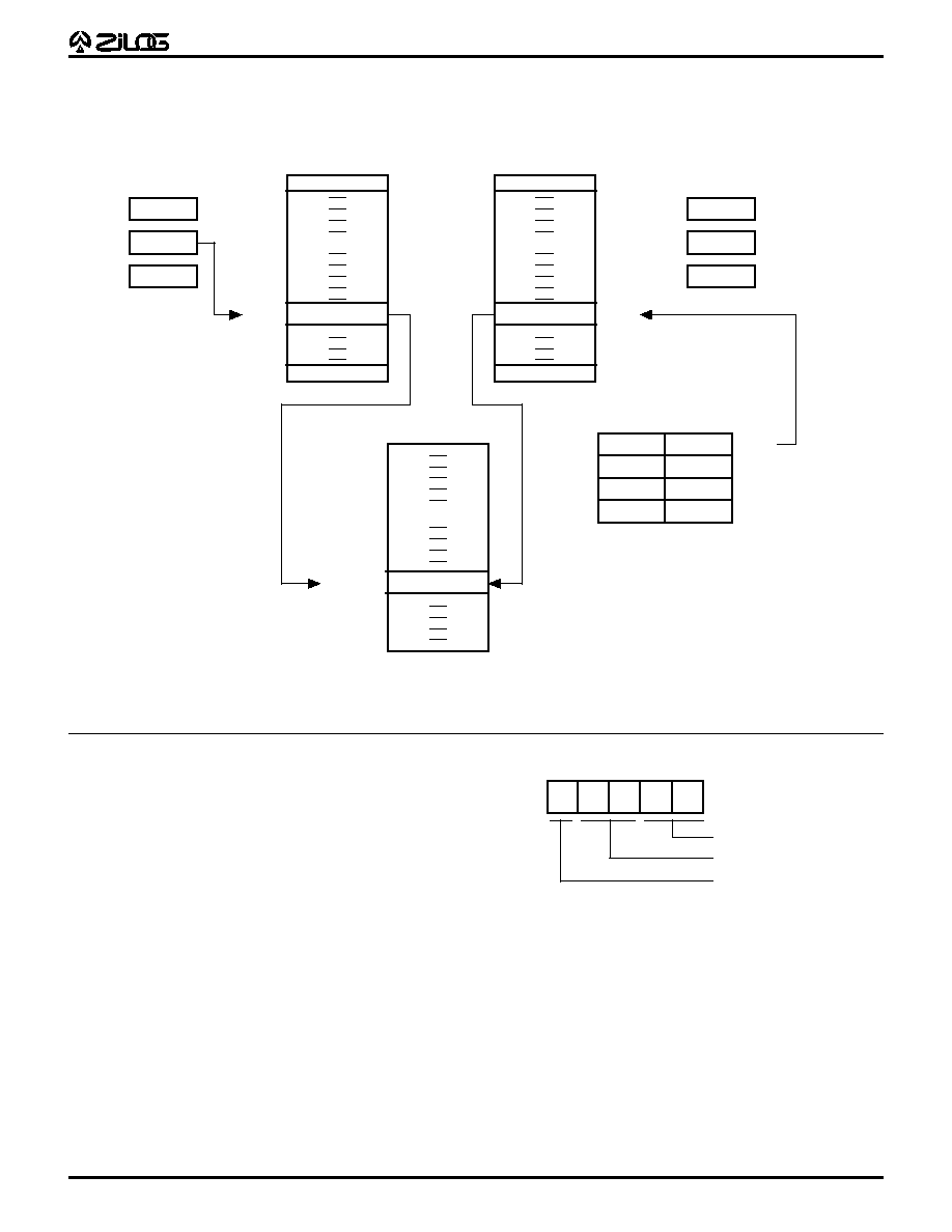
39
Z89323/373/393
16-B
IT
D
IGITAL
S
IGNAL
P
ROCESSORS
P R E L I M I N A R Y
DS95DSP0101 Q4/95
RAM ADDRESSING
The address of the RAM is specified in one of three ways (Figure 22):
RAM Pointers
P0:0
P1:0
P2:0
%37
RAM0
256 x 16-Bit
@P1:0
%0321
%00
RAM1
256 x 16-Bit
%0321
%00
Internal ROM
4K x 16-Bit
%1234
%0000
%1FFF
%0321
@@P1:0
@D0:1
RAM Pointers
P0:1
P1:1
P2:1
D0:0
%0321
D1:0
D2:0
D3:0
D0:1
D1:1
D2:1
D3:1
Data Pointers
%37
%04
S4 / S3 = 01
Each of the following instructions
load %1234 into the Accumulator:
%FF
%FF
LD A,@@P1:0
LD A,@D0:1
Figure 31. RAM, ROM, and Pointer Architecture
Register Indirect
Pn:b n = 0-2, b = 0-1
The most commonly used method is a register indirect
addressing method, where the RAM address is specified
by one of the three RAM address pointers (n) for each bank
(b). Each source/destination field in Figures 6 and 9 may
be used by an indirect instruction to specify a register
pointer and its modification after execution of the instruction.
D3
D2
D1
D0
D8
b
n1
n0
RAM Pointer Register
Operation
RAM Bank
Figure 32. Indirect Register
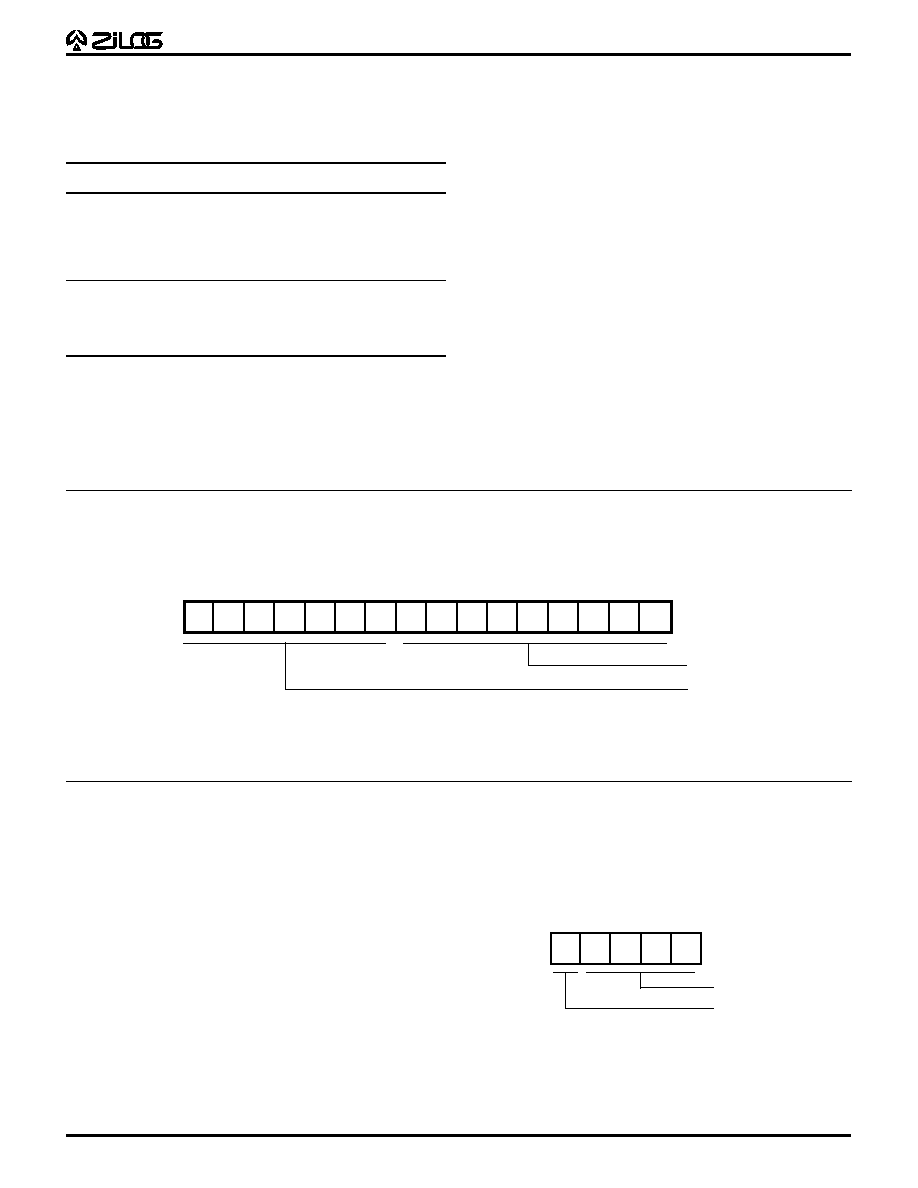
Z89323/373/393
16-B
IT
D
IGITAL
S
IGNAL
P
ROCESSORS
40
P R E L I M I N A R Y
DS95DSP0101 Q4/95
The register pointer is specified by the first and second bits
in the source/destination field and the modification is
specified by the third and fourth bits according to the
following table:
D3-D0
Meaning
00xx
NOP
No Operation
01xx
+ 1
Simple Increment
10xx
≠1/LOOP
Decrement Modulo the Loop Count
11xx
+1/LOOP
Increment Modulo the Loop Count
xx00
P0:0 or P0:1
*
xx01
P1:0 or P1:1
*
xx10
P2:0 or P2:1
*
xx11
See Short Form Direct
Note:
* If bit 8 is zero, P0:0 to P2:0 are selected;
if bit 8 is one, P0:1 to P2:1 are selected.
When LOOP mode is selected, the pointer to which the
loop is referring will cycle up or down, depending on
whether a ≠LOOP or +LOOP is specified. The size of the
loop is obtained from the least significant three bits of the
Status Register. The increment or decrement of the register
is accomplished modulo the loop size. As an example, if
the loop size is specified as 32 by entering the value 101
into bits 2-0 of the Status Register (S2-S0) and an increment
+LOOP is specified in the address field of the instruction,
for example, the RPi field is 11xx, then the register specified
by RPi will increment, but only the least significant five bits
will be affected. This means the actual value of the pointer
will cycle round in a length 32 loop, and the lowest or
highest value of the loop, depending on whether the loop
is up or down, is set by the three most significant bits. This
allows repeated access to a set of data in RAM without
software intervention. To clarify, if the pointer value is
10101001 and if the loop = 32, the pointer increments up
to 10111111, then drops down to 10100000 and starts
again. The upper three bits remaining unchanged. Note
that the original value of the pointer is not retained.
Direct Register
The second method is a direct addressing method. The
address of the RAM is directly specified by the address
field of the instruction. Because this addressing method
consumes nine bits (0-511) of the instruction field, some
instructions cannot use this mode (see Figure 33).
D7
D6
D5
D4
D3
D2
D1
D0
D8
D15 D14 D13 D12 D11 D10 D9
RAM Address
Opcode
Figure 33. Direct Internal RAM Address Format
Short Form Direct
Dn:b n = 0-3, b = 0-1
The last method is called Short Form Direct Addressing,
where one out of 32 addresses in internal RAM can be
specified. The 32 addresses are the 16 lower addresses in
RAM Bank 0 and the 16 lower addresses in RAM Bank 1.
Bit 8 of the instruction field determines RAM Bank 0 or 1.
The 16 addresses are determined by a 4-bit code comprised
of bits S3 and S4 of the status register and the third and
fourth bits of the Source/Destination field. Because this
mode can specify a direct address in a short form, all of the
instructions using the register indirect mode can use this
mode (Figure 30). This method can access only the lower
16 addresses in the both RAM banks and as such has
limited use. The main purpose is to specify a data register,
located in the RAM bank, which can then be used to point
to a program memory location. This facilitates downloading
lookup tables and other instructions from program memory
to RAM.
S4
S3
D3
D2
D8
RAM Address
RAM Bank
b
n3
n2
n1
n0
Figure 34. Short Form Direct Address
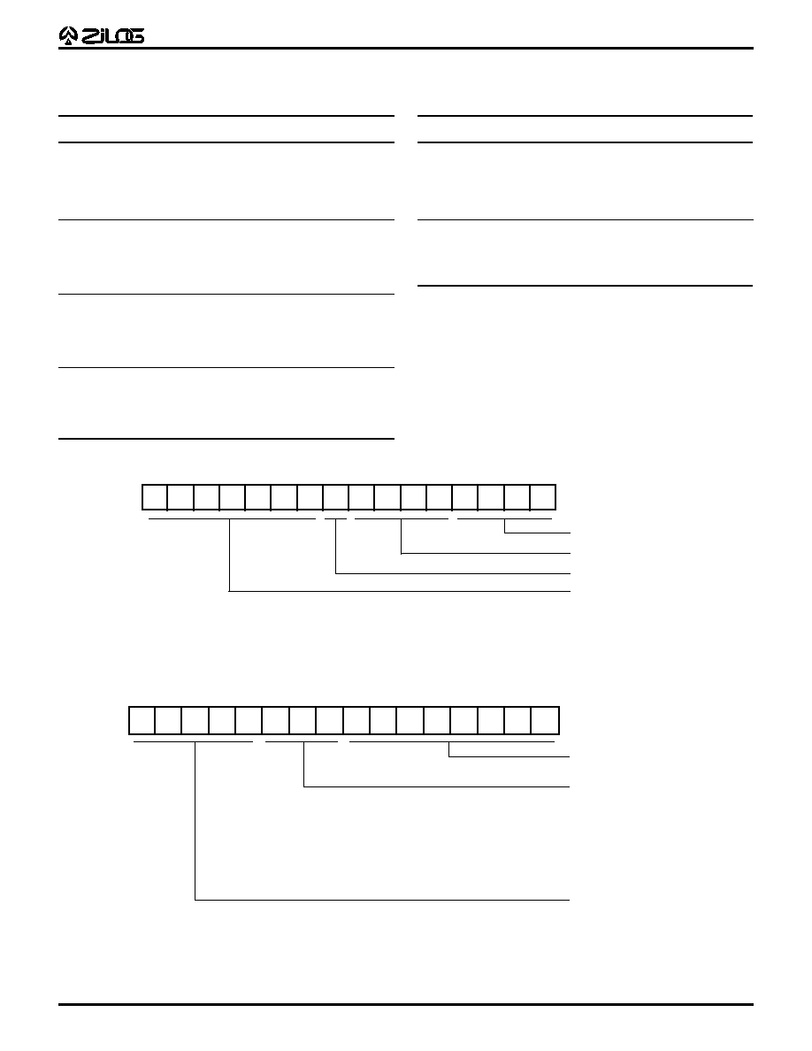
41
Z89323/373/393
16-B
IT
D
IGITAL
S
IGNAL
P
ROCESSORS
P R E L I M I N A R Y
DS95DSP0101 Q4/95
INSTRUCTION FORMAT
Table 13. Registers
Source/Destination
Register
0000
BUS
[1]
0001
X
0010
Y
0011
A
0100
SR
0101
STACK
0110
P C
0111
P
[1]
1000
EXT0
1001
EXT1
1010
EXT2
1011
EXT3
1100
EXT4
1101
EXT5
1110
EXT6
1111
EXT7
Table 14. Register Pointers Field
Source/Destination
Meaning
00xx
NOP
01xx
+ 1
10xx
≠1/LOOP
11xx
+1/LOOP
xx00
P0:0 or P0:1
[2]
xx01
P1:0 or P1:1
[2]
xx10
P2:0 or P2:1
[2]
xx11
Short Form Direct Mode
[3]
Notes:
[1] If RAM Bank bit is 0, then Pn:0 are selected.
If RAM Bank bit is 1, then Pn:1 are selected.
[2] Read only.
[3] When the short form direct mode is selected,
00000-01111 or 10000-11111 are used as RAM addresses.
RAM Bank selection
Destination field
Source field
D15
Opcode
D14 D13 D12 D11 D10
D9
D8
D7
D6
D5
D4
D3
D2
D1
D0
Note: Source/Destination fields can specify either register
or RAM address in RAM pointer indirect mode.
Figure 36. Short Immediate Data Load Format
0 0 0
0 0 1
0 1 0
0 1 1
1 0 0
1 0 1
1 1 0
1 1 1
Reg. Pointer
P0:0
P1:0
P2:0
NA
P0:1
P1:1
P2:1
NA
D7
D6
D5
D4
D3
D2
D1
D0
D8
D15 D14 D13 D12 D11 D10 D9
Short Immediate Data
Opcode
0 0 0 1 1
Figure 35. General Instruction Format
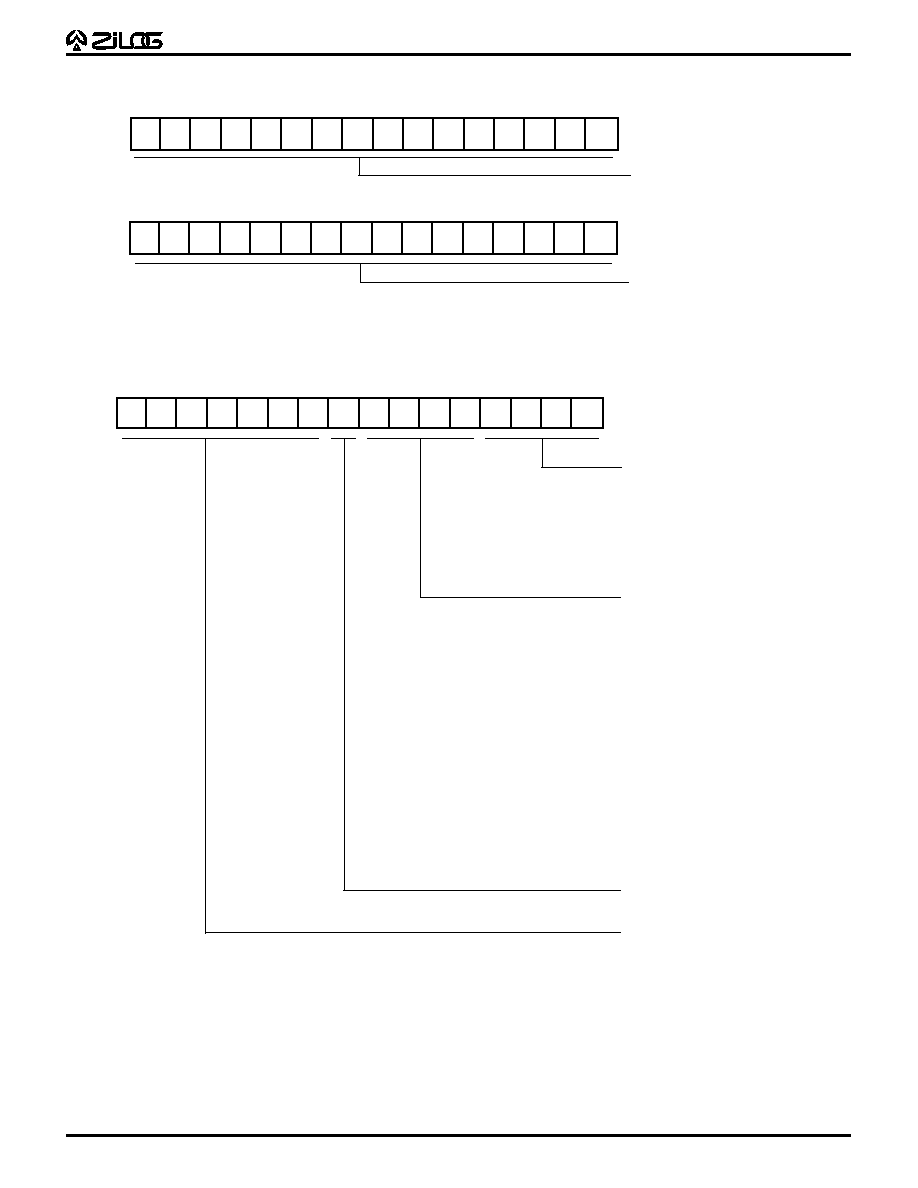
Z89323/373/393
16-B
IT
D
IGITAL
S
IGNAL
P
ROCESSORS
42
P R E L I M I N A R Y
DS95DSP0101 Q4/95
INSTRUCTION FORMAT
(Continued)
D7
D6
D5
D4
D3
D2
D1
D0
D8
D15 D14 D13 D12 D11 D10 D9
1st Word
General Instruction Format
D7
D6
D5
D4
D3
D2
D1
D0
D8
D15 D14 D13 D12 D11 D10 D9
2nd Word
Immediate Data
Figure 37. Immediate Data Load Format
Condition Codes
0 0 0 0 TRUE
0 0 0 1 ----
0 0 1 0 U01=0
0 0 1 1 UO1=0
0 1 0 0 C =0
0 1 0 1 Z=0
0 1 1 0 OV=0
0 1 1 1 N=0
1 x x x - - - -
0 0 0 0 TRUE
0 0 0 1 - - - -
0 0 1 0 UO0=1
0 0 1 1 UO1=1
0 1 0 0 C=1
0 1 0 1 Z=1
0 1 1 0 OV=1
0 1 1 1 N=1
1 x x x - - - -
D7
D6
D5
D4
D3
D2
D1
D0
D8
D15 D14 D13 D12 D11 D10 D9
0 0 0 0
0 0 0 1
0 0 1 0
0 0 1 1
0 1 0 0
0 1 0 1
0 1 1 0
0 1 1 1
ROR Rotate right
ROL Rotate left
SHR Shift right
SHL Shift left
INC Increment (LSB)
DEC Decrement (LSB)
NEG Negate
ABS Absolute
0 = Negative Condition
1 = Positive Condition
Opcode
1 0 0 1 0 0 0
ACC Modification Codes
Figure 38. Accumulator Modification Format
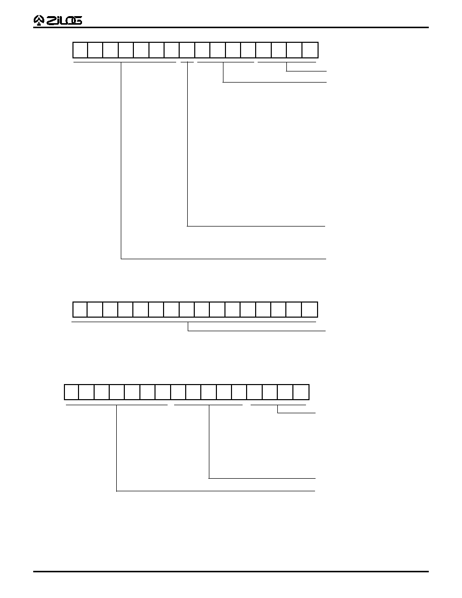
43
Z89323/373/393
16-B
IT
D
IGITAL
S
IGNAL
P
ROCESSORS
P R E L I M I N A R Y
DS95DSP0101 Q4/95
D7
D6
D5
D4
D3
D2
D1
D0
D8
D15 D14 D13 D12 D11 D10 D9
Condition Codes
0 0 0 0 TRUE
0 0 0 1 ----
0 0 1 0 UO0=0
0 0 1 1 UO1=0
0 1 0 0 C=0
0 1 0 1 Z=0
0 1 1 0 OV=0
0 1 1 1 N=0
1 x x x - - - -
0 0 0 0 TRUE
0 0 0 1 - - - -
0 0 1 0 UO0=1
0 0 1 1 UO1=1
0 1 0 0 C=1
0 1 0 1 Z=1
0 1 1 0 OV=1
0 1 1 1 N=1
1 x x x - - - -
x x x x
Condition
0 = Negative
Condition
1 = Positive Condition
Opcode
0 1 0 0 1 1 0
Branch
0 1 0 0 1 0 0 Call
1st Word
D7
D6
D5
D4
D3
D2
D1
D0
D8
D15 D14 D13 D12 D11 D10 D9
2nd Word
Branch Address
Figure 39. Branching Format
x x 1 0
x x 1 1
x 1 x 0
x 1 x 1
1 x x 0
1 x x 1
Reset C flag
Set C flag
Reset IE Flag
(Interrupt enable)
Set IE Flag
Reset OP Flag
(Overflow protection)
Set OP Flag
D7
D6
D5
D4
D3
D2
D1
D0
D8
D15 D14 D13 D12 D11 D10 D9
x x x x
Opcode
1 0 0 1 0 1 0 Mod
Figure 40. Flag Modification Format
Z89323/373/393
16-B
IT
D
IGITAL
S
IGNAL
P
ROCESSORS
44
P R E L I M I N A R Y
DS95DSP0101 Q4/95
ADDRESSING MODES
This section discusses the syntax of the addressing modes
supported by the DSP assembler.
Table 15. Addressing Modes
Symbolic Name
Syntax
Description
< p r e g s >
Pn:b
Pointer Register
< d r e g s >
Dn:b
Data Register
(Points to RAM)
<hwregs>
X,Y,PC,SR,P
Hardware Registers
EXTn,A,BUS
< a c c i n d >
@A
Accumulator Memory Indirect
(Points to Program Memory)
<direct>
<expression>
Direct Address Expression
<limm>
#<const exp>
Long (16-bit) Immediate Value
<simm>
#<const exp>
Short (8-bit) Immediate Value
<regind>
@Pn:b
Pointer Register Indirect
(Points to RAM)
@Pn:b+
Pointer Register Indirect with Increment
@Pn:b≠LOOP
Pointer Register Indirect with Loop Decrement
@Pn:b+LOOP
Pointer register Indirect with Loop Increment
<memind>
@@Pn:b
Pointer Register Memory Indirect
(Points to Program Memory)
@Dn:b
Data Register Memory Indirect
@@Pn:b≠LOOP
Pointer Register Memory Indirect with Loop Decrement
@@Pn:b+LOOP
Pointer Register Memory Indirect with Loop Increment
@@Pn:b+
Pointer Register Memory Indirect with Increment

45
Z89323/373/393
16-B
IT
D
IGITAL
S
IGNAL
P
ROCESSORS
P R E L I M I N A R Y
DS95DSP0101 Q4/95
There are eight distinct addressing modes for data transfer.
<pregs>, <hwregs>
These two modes are used for simple
loads to and from registers within the chip, such as loading
to the Accumulator, or loading from a pointer register. The
names of the registers need only be specified in the
operand field (destination first, then source).
<regind>
This mode is used for indirect accesses to the
data RAM. The address of the RAM location is stored in the
pointer. The "@" symbol indicates "indirect" and precedes
the pointer, therefore @P1:1 instructs the processor to
read or write to a location in RAM1, which is specified by
the value in the pointer.
<dregs>
This mode is also used for accesses to the data
RAM, but only the lower 16 addresses in either bank. The
4-bit address comes from the status register and the
operand field of the data pointer. Note that data registers
are typically used not for addressing RAM, but loading
data from program memory space.
<memind>
This mode is used for indirect accesses to the
program memory. The address of the memory is located
in a RAM location, which is specified by the value in a
pointer. Therefore, @@P1:1 instructs the processor to
read (write is not possible) from a location in memory,
which is specified by a value in RAM, and the location of
the RAM is in turn specified by the value in the pointer.
Note that the data pointer can also be used for a memory
access in this manner, but only one "@" precedes the
pointer. In both cases, the memory address stored in RAM
is incremented by one, each time the addressing mode is
used, to allow easy transfer of sequential data from
program memory.
<accind>
Similar to the previous mode, the address for the
program memory read is stored in the Accumulator. @A in
the second operand field loads the number in memory
specified by the address in A.
<direct>
The direct mode allows read or write to data RAM
from the Accumulator by specifying the absolute address
of the RAM in the operand of the instruction. A number
between 0 and 255 indicates a location in RAM0, and a
number between 256 and 511 indicates a location in
RAM1.
<limm>
This address mode indicates a long immediate
load. A 16-bit word can be copied directly from the
operand into the specified register or memory.
<simm>
This address mode can only be used for immediate
transfer of 8-bit data in the operand to the specified RAM
pointer.
CONDITION CODES
The following Instruction Description defines the condition
codes supported by the DSP assembler. If the instruction
description refers to the <cc> (condition code) symbol in
one of its addressing modes, the instruction will only
execute if the condition is true.
Code
Description
C
Carry
EQ
Equal (same as Z)
F
False
IE
Interrupts Enabled
MI
Minus
NC
No Carry
NE
Not Equal (same as NZ)
NIE
Not Interrupts Enabled
NOV
Not Overflow
NU0
Not User Zero
Code
Description
NU1
Not User One
NZ
Not zero
OV
Overflow
PL
Plus (Positive)
U0
User Zero
U1
User One
UGE
Unsigned Greater Than or
Equal (Same as NC)
ULT
Unsigned Less Than (Same as C)
Z
Zero

Z89323/373/393
16-B
IT
D
IGITAL
S
IGNAL
P
ROCESSORS
46
P R E L I M I N A R Y
DS95DSP0101 Q4/95
INSTRUCTION DESCRIPTIONS
Inst.
Description
Synopsis
Operands
Words Cycles
Examples
ABS
Absolute Value
ABS[<cc>,]<src>
<cc>,A
1
1
ABS NC,A
A
1
1
ABS A
ADD
Addition
ADD<dest>,<src>
A,<pregs>
1
1
ADD A,P0:0
A,<dregs>
1
1
ADD A,D0:0
A,<limm>
2
2
ADD A,#%1234
A,<memind>
1
3
ADD A,@@P0:0
A,<direct>
1
1
ADD A,%F2
A,<regind>
1
1
ADD A,@P1:1
A,<hwregs>
1
1
ADD A,X
A, <simm>
ADD A, #%12
AND
Bitwise AND
AND<dest>,<src>
A,<pregs>
1
1
AND A,P2:0
A,<dregs>
1
1
AND A,D0:1
A,<limm>
2
2
AND A,#%1234
A,<memind>
1
3
AND A,@@P1:0
A,<direct>
1
1
AND A,%2C
A,<regind>
1
1
AND A,@P1:2+LOOP
A,<hwregs>
1
1
AND A,EXT3
A, <simm>
AND A, #%12
CALL
Subroutine call
CALL [<cc>,]<address>
<cc>,<direct>
2
2
CALL Z,sub2
<direct>
2
2
CALL sub1
CCF
Clear carry flag
CCF
None
1
1
CCF
CIEF
Clear Carry Flag
CIEF
None
1
1
CIEF
COPF
Clear OP flag
COPF
None
1
1
COPF
CP
Comparison
CP<src1>,<src2>
A,<pregs>
1
1
CP A,P0:0
A,<dregs>
1
1
CP A,D3:1
A,<memind>
1
3
CP A,@@P0:1
A,<direct>
1
1
CP A,%FF
A,<regind>
1
1
CP A,@P2:1+
A,<hwregs>
1
1
CP A,STACK
A<limm>
2
2
CP A,#%FFCF
A, <simm>
CP A, #%12
DEC
Decrement
DEC [<cc>,]<dest>
<cc>A,
1
1
DEC NZ,A
A
1
1
DEC A
INC
Increment
INC [<cc>,] <dest>
<cc>,A
1
1
INC PL,A
A
1
1
INC A
JP
Jump
JP [<cc>,]<address>
<cc>,<direct>
2
2
JP NIE,Label
<direct>
2
2
JP Label

47
Z89323/373/393
16-B
IT
D
IGITAL
S
IGNAL
P
ROCESSORS
P R E L I M I N A R Y
DS95DSP0101 Q4/95
Inst. Description
Synopsis
Operands
Words Cycles Examples
LD
Load destination
LD<dest>,<src>
A,<hwregs>
1
1
LD A,X
with source
A,<dregs>
1
1
LD A,D0:0
A,<pregs>
1
1
LD A,P0:1
A,<regind>
1
1
LD A,@P1:1
A,<memind>
1
3
LD A,@D0:0
A,<direct>
1
1
LD A,124
<direct>,A
1
1
LD 124,A
<dregs>,<hwregs>
1
1
LD D0:0,EXT7
<pregs>,<simm>
1
1
LD P1:1,#%FA
<pregs>,<hwregs>
1
1
LD P1:1,EXT1
<regind>,<limm>
1
1
LD@P1:1,#1234
<regind>,<hwregs>
1
1
LD @P1:1+,X
<hwregs>,<pregs>
1
1
LD Y,P0:0
<hwregs>,<dregs>
1
1
LD SR,D0:0
<hwregs>,<limm>
2
2
LD PC,#%1234
<hwregs>,<accind>
1
3
LD X,@A
<hwregs>,<memind>
1
3
LD Y,@D0:0
<hwregs>,<regind>
1
1
LD A,@P0:0≠LOOP
<hwregs>,<hwregs>
1
1
LD X,EXT6
Note:
When <dest> is <hwregs>, <dest> cannot be P.
Note:
When <dest> is <hwregs> and <src> is <hwregs>, <dest> cannot be EXTn
if <src> is EXTn, <dest> cannot be X if <src> is X, <dest> cannot be SR
if <src> is SR.
Note:
When <src> is <accind> <dest> cannot be A.
MLD
Multiply
MLD<srcl>,<srcl>[,<bank switch>]
<hwregs>,<regind>
1
1
MLD A,@P0:0+LOOP
<hwregs>,<regind>,<bank switch> 1
1
MLD A,@P1:0,OFF
<regind>,<regind>
1
1
MLD @P1:1,@P2:0
<regind>,<regind>,<bank switch>
1
1
MLD @P0:1,@P1:0,ON
Note:
If src1 is <regind> it must be a bank 1 register. Src2's <regind must be
a bank 0 register.
Note:
<hwregs> for src1 cannot be X.
Note:
For the operands <hwregs>, <regind> the <band switch> defaults to OFF.
For the operands <regind>, the <bank switch> defaults to ON.
MPYA
Multiply and add
MPYA <srcl>,<src2>[,<bank switch>]
<hwregs>,<regind>
1
1
MPYA A,@P0:0
<hwregs>,<regind>,<bank switch> 1
1
MPYA A,@P1:0,OFF
<regind>,<regind>
1
1
MPYA @P1:1,@P2:0
<regind>,<regind>,<bank switch>
1
1
MPYA@P0:1,@P1:0,ON
Note:
If src1 is <regind> it must be a bank 1 register. Src2's <regind> must be
a bank 0 register.
Note:
<hwregs> for src1 cannot be X.
Note:
For the operands <hwregs>, <regind> the <bank switch> defaults to OFF.
For the operands <regind>, the <bank switch> defaults to ON.

Z89323/373/393
16-B
IT
D
IGITAL
S
IGNAL
P
ROCESSORS
48
P R E L I M I N A R Y
DS95DSP0101 Q4/95
INSTRUCTION DESCRIPTIONS
(Continued)
Inst. Description
Synopsis
Operands
Words Cycles Examples
MPYS
Multiply and
MPYS<src1>,<src2>[,<bank switch>]
<hwregs>,<regind>
1
1
MPYS A,@P0:0
subtract
<hwregs>,<regind>,<bank switch> 1
1
MPYS A,@P1:0,OFF
<regind>,<regind>
1
1
MPYS @P1:1,@P2:0
<regind>,<regind>,<bank switch>
1
1
MPYS @P0:1,@P1:0,ON
Note:
If src1 is <regind> it must be a bank 1 register. Src2's <regind> must be
a bank 0 register.
Note:
<hwregs> for src1 cannot be X.
Note:
For the operands <hwregs>, <regind> the <bank switch> defaults to OFF.
For the operands <regind>, <regind> the <bank switch> defaults to ON.
NEG
Negate
NEG <cc>,A
<cc>, A
1
1
NEG MI,A
A
1
1
NEG A
NOP
No operation
NOP
None
1
1
NOP
OR
Bitwise OR
OR <dest>,<src>
A, <pregs>
1
1
OR A,P0:1
A, <dregs>
1
1
OR A, D0:1
A, <limm>
2
2
OR A,#%2C21
A, <memind>
1
3
OR A,@@P2:1+
A, <direct>
1
1
OR A, %2C
A, <regind>
1
1
OR A,@P1:0≠LOOP
A, <hwregs>
1
1
OR A,EXT6
A, <simm>
OR A,#%12
POP
Pop value
POP <dest>
<pregs>
1
1
POP P0:0
from stack
<dregs>
1
1
POP D0:1
<regind>
1
1
POP @P0:0
<hwregs>
1
1
POP A
PUSH
Push value
PUSH <src>
<pregs>
1
1
PUSH P0:0
onto stack
<dregs>
1
1
PUSH D0:1
<regind>
1
1
PUSH @P0:0
<hwregs>
1
1
PUSH BUS
<limm>
2
2
PUSH #12345
<accind>
1
3
PUSH @A
<memind>
1
3
PUSH @@P0:0
RET
Return from subroutine
RET
None
1
2
RET
RL
Rotate Left
RL <cc>,A
<cc>,A
1
1
RL NZ,A
A
1
1
RL A
RR
Rotate Right
RR <cc>,A
<cc>,A
1
1
RR C,A
A
1
1
RR A

49
Z89323/373/393
16-B
IT
D
IGITAL
S
IGNAL
P
ROCESSORS
P R E L I M I N A R Y
DS95DSP0101 Q4/95
Inst. Description
Synopsis
Operands
Words
Cycles Examples
SCF
Set C flag
SCF
None
1
1
SCF
SIEF
Set IE flag
SIEF
None
1
1
SIEF
SLL
Shift left
SLL
[<cc>,]A
1
1
SLL NZ,A
logical
A
1
1
SLL A
SOPF
Set OP flag
SOPF
None
1
1
SOPF
SRA
Shift right
SRA<cc>,A
<cc>,A
1
1
SRA NZ,A
arithmetic
A
1
1
SRA A
SUB
Subtract
SUB<dest>,<src>
A,<pregs>
1
1
SUB A,P1:1
A,<dregs>
1
1
SUB A,D0:1
A,<limm>
2
2
SUB A,#%2C2C
A, <memind>
1
3
SUB A,@D0:1
A, <direct>
1
1
SUB A,%15
A, <regind>
1
1
SUB A,@P2:0≠LOOP
A, <hwregs>
1
1
SUB A,STACK
A, <simm>
SUB A, #%12
XOR
Bitwise exclusive OR
XOR <dest>,<src>
A, <pregs>
1
1
XOR A,P2:0
A, <dregs>
1
1
XOR A,D0:1
A, <limm>
2
2
XOR A,#13933
A, <memind>
1
3
XOR A,@@P2:1+
A, <direct>
1
1
XOR A,%2F
A, <regind>
1
1
XOR A,@P2:0
A, <hwregs>
1
1
XOR A,BUS
A, <simm>
XOR A, #%12
Bank Switch Enumerations.
The third (optional) operand
of the MLD, MPYA and MPYS instructions represents
whether a bank switch is set ON or OFF. To more clearly
represent this, the keywords ON and OFF are used to state
the direction of the switch. These keywords are referenced
in the instruction descriptions through the <bank switch>
symbol. The most notable capability this provides is that a
source operand can be multiplied by itself (squared).
Z89323/373/393
16-B
IT
D
IGITAL
S
IGNAL
P
ROCESSORS
50
P R E L I M I N A R Y
DS95DSP0101 Q4/95
ABSOLUTE MAXIMUM RATINGS
Symbol
Description
Min.
Max.
Units
V
CC
Supply Voltage (*)
≠0.3
+7.0
V
T
STG
Storage Temp
≠65
∞
+150
∞
C
T
A
Oper Ambient Temp
∞
C
Notes:
* Voltage on all pins with respect to GND.
See Ordering Information.
Stresses greater than those listed under Absolute Maximum
Ratings may cause permanent damage to the device. This
is a stress rating only; operation of the device at any
condition above those indicated in the operational sections
of these specifications is not implied. Exposure to absolute
maximum rating conditions for extended period may affect
device reliability.
STANDARD TEST CONDITIONS
The characteristics listed below apply for standard test
conditions as noted. All voltages are referenced to Ground.
Positive current flows into the referenced pin (Figure 41).
DC ELECTRICAL CHARACTERISTICS (20 MHZ)
(V
DD
= 5V
±
10%, T
A
= 0
∞
C to +70
∞
C, unless otherwise noted.)
fclock = 20 MHz
Standard Temp
Extended Temp
T
A
= 0
∞
to +70
∞
C
T
A
= ≠40
∞
to +85
∞
C
Symbol
Parameter
Condition
Min.
Max.
Min.
Max.
Units
I
DD
Supply Current
V
DD
= 5.5V
60
55
mA
I
DC
DC Power Consumption
5
5
mA
V
IH
Input High Level
2.7
2.7
V
V
IL
Input Low Level
.8
.8
V
IL
Input Leakage
10
10
µ
A
V
OH
Output High Voltage
I
OH
= ≠100
µ
A
V
DD
-0.2
V
DD
-02
V
V
OL
Input Low Voltage
I
OL
= 2.0 mA
.5
.5
V
I
FL
Output Floating
Leakage Current
10
10
µ
A
+5V
From Output
Under Test
30 pF
9.1 kOhm
2.1 kOhm
Figure 41. Test Load Diagram

51
Z89323/373/393
16-B
IT
D
IGITAL
S
IGNAL
P
ROCESSORS
P R E L I M I N A R Y
DS95DSP0101 Q4/95
AC ELECTRICAL CHARACTERISTICS (20 MHZ)
(V
DD
= 5V
±
10%, T
A
= 0
∞
C to +70
∞
C, unless otherwise noted.)
Standard Temp
T
A
= 0
∞
to +70
∞
C
Symbol
Parameter
Min.
Max.
Units
Clock
TCY
Clock Cycle Time
5 0
n s
Tr
Clock Rise Time
2
n s
Tf
Clock Fall Time
2
n s
CPW
Clock Pulse Width
2 3
n s
I/O
DSVALID
/DS Valid Time from CLOCK Fall
0
1 5
n s
DSHOLD
/DS Valid Time from CLOCK Rise
4
1 5
n s
EASET
EA Setup Time to /DS Fall
1 2
n s
EAHOLD
EA Hold Time from /DS Rise
4
n s
RDSET
Data Read Setup Time to /DS Rise
1 4
n s
RDHOLD
Data Read Hold Time from /DS Fall
6
n s
WRVALID
Data Write Valid Time from /DS Fall
1 8
n s
WRHOLD
Data Write Hold Time from /DS Rise
5
n s
Interrupt
INTSET
Interrupt Setup Time to CLOCK Fall
7
n s
INTWIDTH
Interrupt Low Pulse Width
1 TCY
n s
Reset
RRise
Reset Rise Time
1000
n s
RSET
Reset Setup Time to CLOCK Rise
1 5
n s
RWIDTH
Interrupt Low Pulse Width
2 TCY
n s
Wait State
WSET
Wait Setup Time to CLOCK Rise
2 3
n s
WHOLD
Wait Hold Time from CLOCK Rise
1
n s
Halt
HSET
Halt Setup Time to CLOCK Rise
3
n s
HHOLD
Halt Hold Time from CLOCK Rise
1 0
n s

Z89323/373/393
16-B
IT
D
IGITAL
S
IGNAL
P
ROCESSORS
52
P R E L I M I N A R Y
DS95DSP0101 Q4/95
AC ELECTRICAL CHARACTERISTICS (20 MHZ)
(Continued)
(V
DD
= 5V
±
10%, T
A
= 0
∞
C to +70
∞
C, unless otherwise noted.)
Analog to Digital
Min.
Typical
Max
Units
Resolution
8
Bits
Integral Non-Linearity
0.5
1
LSB
Differential Non-Linearity
0.5
1
LSB
Zero Error at 25
∞
C
4 5
mV
Supply Range
4.5
5.0
5.5
Volts
Power Dissipation, No Load
5 0
8 5
mW
Clock Frequency
3 3
MHz
Input Voltage Range
VALO
VAHI
Volts
Conversion Time
2
µ
s e c
Input Capacitance on ANA
2 5
4 0
p F
VAHI Range
VALO +2.5
ANVCC
Volts
VALO Range
ANGND
ANVCC ≠2.5
Volts
VAHI-VALO
2.5
ANVCC
Volts
DC ELECTRICAL CHARACTERISTICS (10 MHZ)
(V
DD
= 5V
±
10%, T
A
= 0
∞
C to +70
∞
C, unless otherwise noted.)
fclock = 10 MHz
Standard Temp
Extended Temp
T
A
= 0
∞
to +70
∞
C
T
A
= ≠40
∞
to +85
∞
C
Symbol
Parameter
Condition
Min.
Max.
Min.
Max.
Units
I
DD
Supply Current
V
DD
= 5.5V
30
55
mA
I
DC
DC Power Consumption
5
5
mA
V
IH
Input High Level
2.7
2.7
V
V
IL
Input Low Level
.8
.8
V
IL
Input Leakage
10
10
µ
A
V
OH
Output High Voltage
I
OH
= ≠100
µ
A
V
DD
-0.2
V
DD
-02
V
V
OL
Input Low Voltage
I
OL
= 2.0 mA
.5
.5
V
I
FL
Output Floating
Leakage Current
10
10
µ
A

53
Z89323/373/393
16-B
IT
D
IGITAL
S
IGNAL
P
ROCESSORS
P R E L I M I N A R Y
DS95DSP0101 Q4/95
AC ELECTRICAL CHARACTERISTICS (10 MHZ)
(V
DD
= 5V
±
10%, T
A
= 0
∞
C to +70
∞
C, unless otherwise noted.)
Standard Temp
T
A
= 0
∞
to +70
∞
C
Symbol
Parameter
Min.
Max.
Units
Clock
TCY
Clock Cycle Time
100
n s
Tr
Clock Rise Time
2
n s
Tf
Clock Fall Time
2
n s
CPW
Clock Pulse Width
4 8
n s
I/O
DSVALID
/DS Valid Time from CLOCK Fall
0
2 5
n s
DSHOLD
/DS Valid Time from CLOCK Rise
6
2 5
n s
EASET
EA Setup Time to /DS Fall
1 8
n s
EAHOLD
EA Hold Time from /DS Rise
6
n s
RDSET
Data Read Setup Time to /DS Rise
2 1
n s
RDHOLD
Data Read Hold Time from /DS Fall
9
n s
WRVALID
Data Write Valid Time from /DS Fall
3 0
n s
WRHOLD
Data Write Hold Time from /DS Rise
8
n s
Interrupt
INTSET
Interrupt Setup Time to CLOCK Fall
1 1
n s
INTWIDTH
Interrupt Low Pulse Width
1 TCY
n s
Reset
RRise
Reset Rise Time
1500
n s
RSET
Reset Setup Time to CLOCK Rise
2 2
n s
RWIDTH
Interrupt Low Pulse Width
2 TCY
n s
Wait State
WSET
Wait Setup Time to CLOCK Rise
3 5
n s
WHOLD
Wait Hold Time from CLOCK Rise
2
n s
Halt
HSET
Halt Setup Time to CLOCK Rise
5
n s
HHOLD
Halt Hold Time from CLOCK Rise
1 5
n s
Analog to Digital
Min.
Typical
Max
Units
Resolution
8
Bits
Integral Non-Linearity
0.5
1
LSB
Differential Non-Linearity
0.5
1
LSB
Zero Error at 25
∞
C
4 5
mV
Supply Range
4.5
5.0
5.5
Volts
Power Dissipation, No Load
5 0
8 5
mW
Clock Frequency
3 3
MHz
Input Voltage Range
VALO
VAHI
Volts
Conversion Time
2
µ
s e c
Input Capacitance on ANA
2 5
4 0
p F
VAHI Range
VALO +2.5
ANVCC
Volts
VALO Range
ANGND
ANVCC ≠2.5
Volts
VAHI-VALO
2.5
ANVCC
Volts
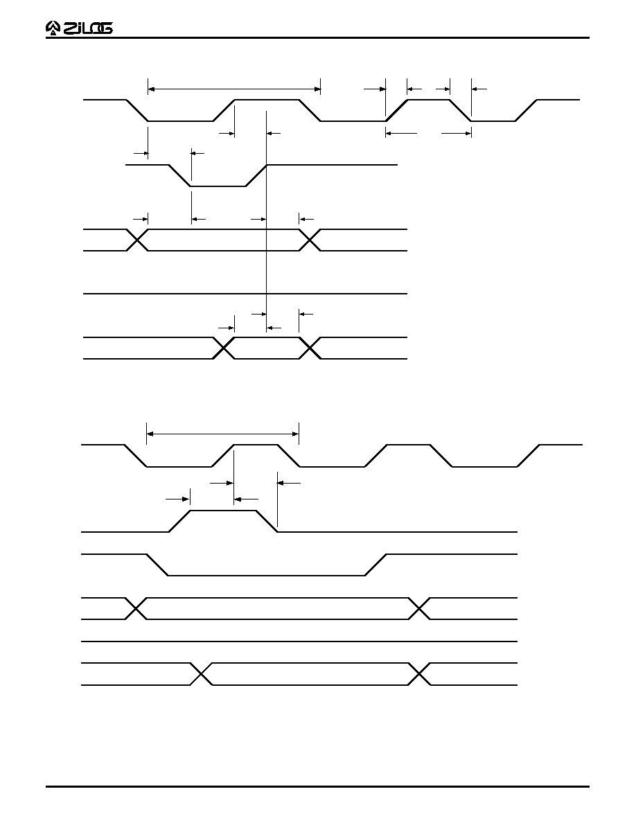
Z89323/373/393
16-B
IT
D
IGITAL
S
IGNAL
P
ROCESSORS
54
P R E L I M I N A R Y
DS95DSP0101 Q4/95
TCY
Tr
Tf
CPW
DSHOLD
DSVALID
EASET
EAHOLD
RDSET
RDHOLD
Data In
Valid Address Out
CLOCK
/DS
EA(2:0)
RD//WR
EXT(15:0)
Figure 42. Read Timing
TCY
WSET
WHOLD
Valid Address Out
Data In
CLOCK
WAIT
/DS
EA(2:0)
RD//WR
EXT(15:0)
TIMING DIAGRAMS
Figure 43. Read Timing Using WAIT Pin

55
Z89323/373/393
16-B
IT
D
IGITAL
S
IGNAL
P
ROCESSORS
P R E L I M I N A R Y
DS95DSP0101 Q4/95
TCY
DSHOLD
DSVALID
EASET
EAHOLD
WRVALID
WRHOLD
Data In
Valid Address Out
EAHOLD
EASET
EXT(15:0)
RD//WR
EA(2:0)
/DS
CLOCK
Figure 44. Write Timing
TCY
WSET
WHOLD
Valid Address Out
Data In
CLOCK
WAIT
/DS
EA(2:0)
RD//WR
EXT(15:0)
Figure 45. Write Timing Using WAIT Pin
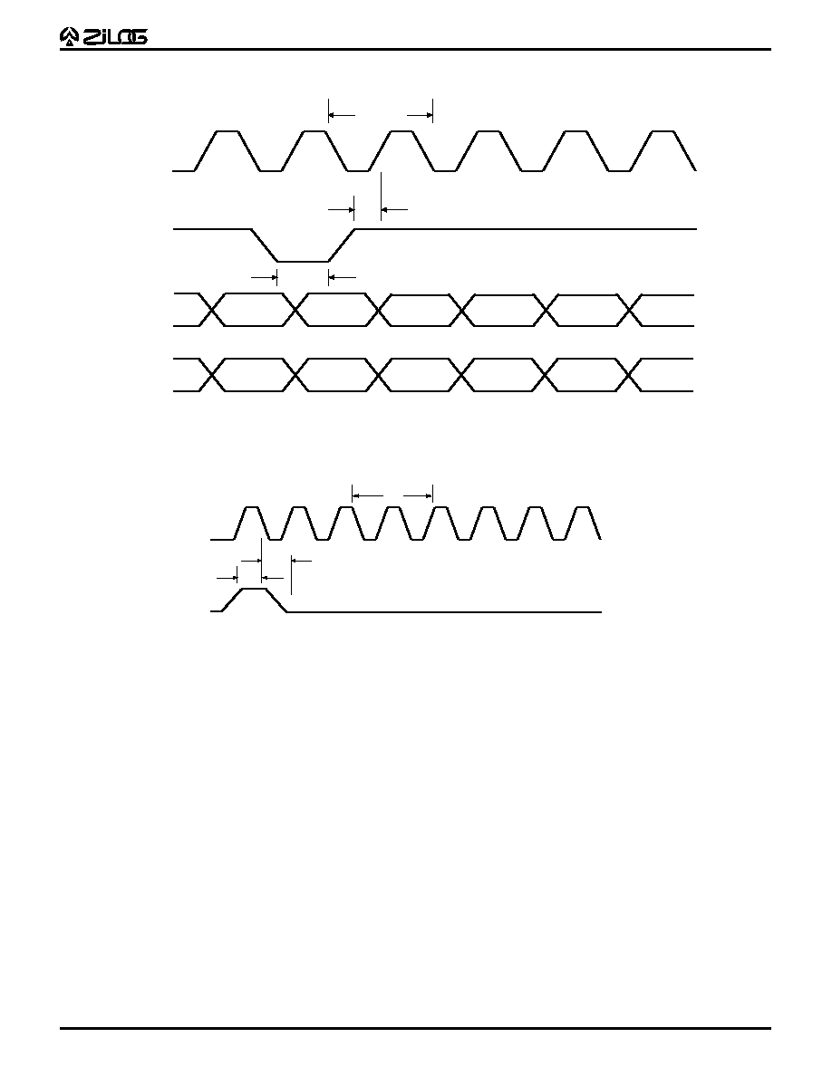
Z89323/373/393
16-B
IT
D
IGITAL
S
IGNAL
P
ROCESSORS
56
P R E L I M I N A R Y
DS95DSP0101 Q4/95
TIMING DIAGRAMS
(Continued)
TCY
INTWidth
INTSET
Fetch N ≠1
Fetch N
Fetch N +1
Fetch Int_Addr
Fetch I
Fetch I +1
Execute N ≠1
Execute N
CALL Int Routine
Execute Int Routine
CLOCK
INT 0,1,2
PROGRAM
ADDRESS
EXECUTE
TCY
HHOLD
HSET
CLOCK
HALT
Figure 46. Interrupt Timing
Figure 47. HALT Timing
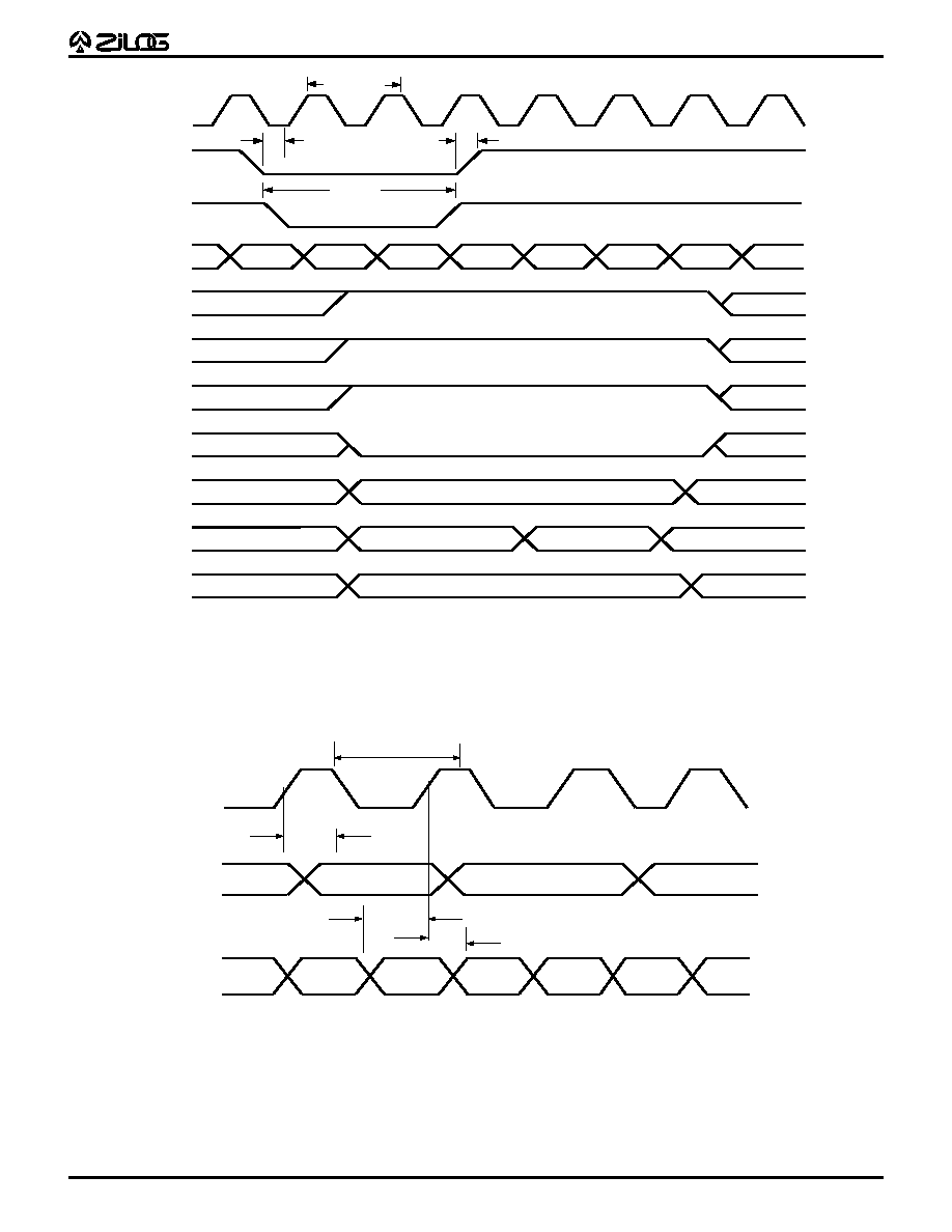
57
Z89323/373/393
16-B
IT
D
IGITAL
S
IGNAL
P
ROCESSORS
P R E L I M I N A R Y
DS95DSP0101 Q4/95
Cycle 0
Cycle 1
Cycle 2
Cycle 3
Cycle 4
Cycle 5
Code Exec
Tri-Stated
Tri-Stated
Access Reset Vector
Intact*
* The RAM and hardware registers are left intact
during a warm reset. A cold reset will produce
random data in these locations. The status
register is set to zeroes in both cases.
CLOCK
/RESET
INTERNAL
RESET
EXECUTE
RD//WR
/DS
UO0-1
EA0-2
EXT0-15
PA0-15
RAM/
REGISTERS
TCY
RSET
RRISE
RWIDTH
Figure 48. RESET Timing
PDSET
PDHOLD
Valid
Valid
Valid
PAVALID
CLOCK
PROGRAM
ADDRESS
PROGRAM
DATA
TCY
Valid
Valid
Valid
Figure 49. External Program Memory Port Timing

Z89323/373/393
16-B
IT
D
IGITAL
S
IGNAL
P
ROCESSORS
58
P R E L I M I N A R Y
DS95DSP0101 Q4/95
PACKAGE INFORMATION
44-Pin PLCC Package Diagram
68-Pin PLCC Package Diagram

59
Z89323/373/393
16-B
IT
D
IGITAL
S
IGNAL
P
ROCESSORS
P R E L I M I N A R Y
DS95DSP0101 Q4/95
44-Pin QFP Package Diagram
80-Pin QFP Package Diagram

Z89323/373/393
16-B
IT
D
IGITAL
S
IGNAL
P
ROCESSORS
60
P R E L I M I N A R Y
DS95DSP0101 Q4/95
PACKAGE INFORMATION
(Continued)
100-Pin QFP Package Diagram

61
Z89323/373/393
16-B
IT
D
IGITAL
S
IGNAL
P
ROCESSORS
P R E L I M I N A R Y
DS95DSP0101 Q4/95
ORDERING INFORMATION
Z89323
Z89373
Z89393
44-Pin PLCC
44-Pin PLCC
100-Pin PQFP
Z8932320VSC
Z8937316VSC
Z8939320FSC
Z8932320VEC
68-Pin PLCC
68-Pin PLCC
Z893232XVSC
Z893731XVSC
Z893232XVEC
44-Pin PQFP
44-Pin PQFP
Z8932320FSC
Z8937316FSC
Z8932320FEC
80-Pin PQFP
80-Pin PQFP
Z893232YFSC
Z893731YFSC
Z893232YFEC
For fast results, contact your local Zilog sales office for
assistance in ordering the part desired.
Package
V = Plastic PLCC
F = Plastic QFP
Temperature
S = 0
∞
C to +70
∞
C
E = ≠40
∞
C to +85
∞
C
Speed
16 = 16 MHz
20 = 20 MHz
Environmental
C = Plastic Standard
Example:
Z 89323 20 V S C
Environmental Flow
Temperature
Package
Speed / Bond Out Option*
Product Number
Zilog Prefix
is a Z89323, 20 MHz, PLCC, 0
∞
C to +70
∞
C, Plastic Standard Flow
* 2X = 20 MHz, 68-pin PLCC style package
20 = 20 MHz, 44-pin package
2Y = 20 MHz, 80-Pin PQFP style package
1X = 16 MHz, 68-Pin PLCC style package
16 = 16 MHz, 44-Pin package
1Y = 16 MHz 80-Pin PQFP style package