 | –≠–ª–µ–∫—Ç—Ä–æ–Ω–Ω—ã–π –∫–æ–º–ø–æ–Ω–µ–Ω—Ç: Z8C520 | –°–∫–∞—á–∞—Ç—å:  PDF PDF  ZIP ZIP |
Document Outline
- Preliminary Product Specification
- Z8E520/C520
- 1.5 MBPS USB Low-Power Device Controller For Multi...
- Part
- ROM
- RAM
- Speed
- Number
- (KB)
- (Bytes)
- (MHz)
- Z8E520 (OTP)
- Z8C520 (ROM)
- Six Vectored Interrupts with Fixed Priority
- Processor Speed Dividable by Firmware Control
- Operating Current: 5 mA typical in USB Mode; 2.5 m...
- 16 Total Input/Output Pins (Open-Drain/Push-Pull) ...
- 6 inputs with 3 level Programmable Reference Compa...
- 16-Bit Programmable Watch-Dog Timer (WDT) with Int...
- Software Programmable Timers Configurable as:
- Two 8-Bit Standard Timers and One 16-Bit Ö Stand...
- One 16-Bit Standard Timer and One 16-Bit Pulse Ö...
- Identical Masked ROM Version (Z8C520)
- On-Chip Oscillator that accepts a Ceramic Resonato...
- Hardware Support for PS/2, Serial, USB, and Genera...
- Power Reduction Modes:
- STOP Mode (functionality shut down except SMR)
- HALT Mode (XTAL still running-peripherals active...
- USB SIE Compliant with USB Spec 1.0
- 4.0 VDC to 6.0 VDC Operating Range @ 0∞C to +70∞C
- Zilogês Z8E520 (OTP) and Z8C520 (Masked ROM) micro...
- For applications demanding powerful I/O capabiliti...
- Both 8-bit and 16-bit timers, with a large number ...
- The microcontroller clock frequency is derived fro...
- The device is capable of functioning in four disti...
- Power connections follow conventional descriptions...
- Connection
- Circuit
- Device
- Communication Modes
- The Z8E520/C520 allows its user to function in a v...
- PS/2 Mode. The serial baud rate is fixed at 12.5 K...
- RS232 Mode. The data rate is fixed at 1200 baud. T...
- GPIO Mode. In General-Purpose I/O Mode, the serial...
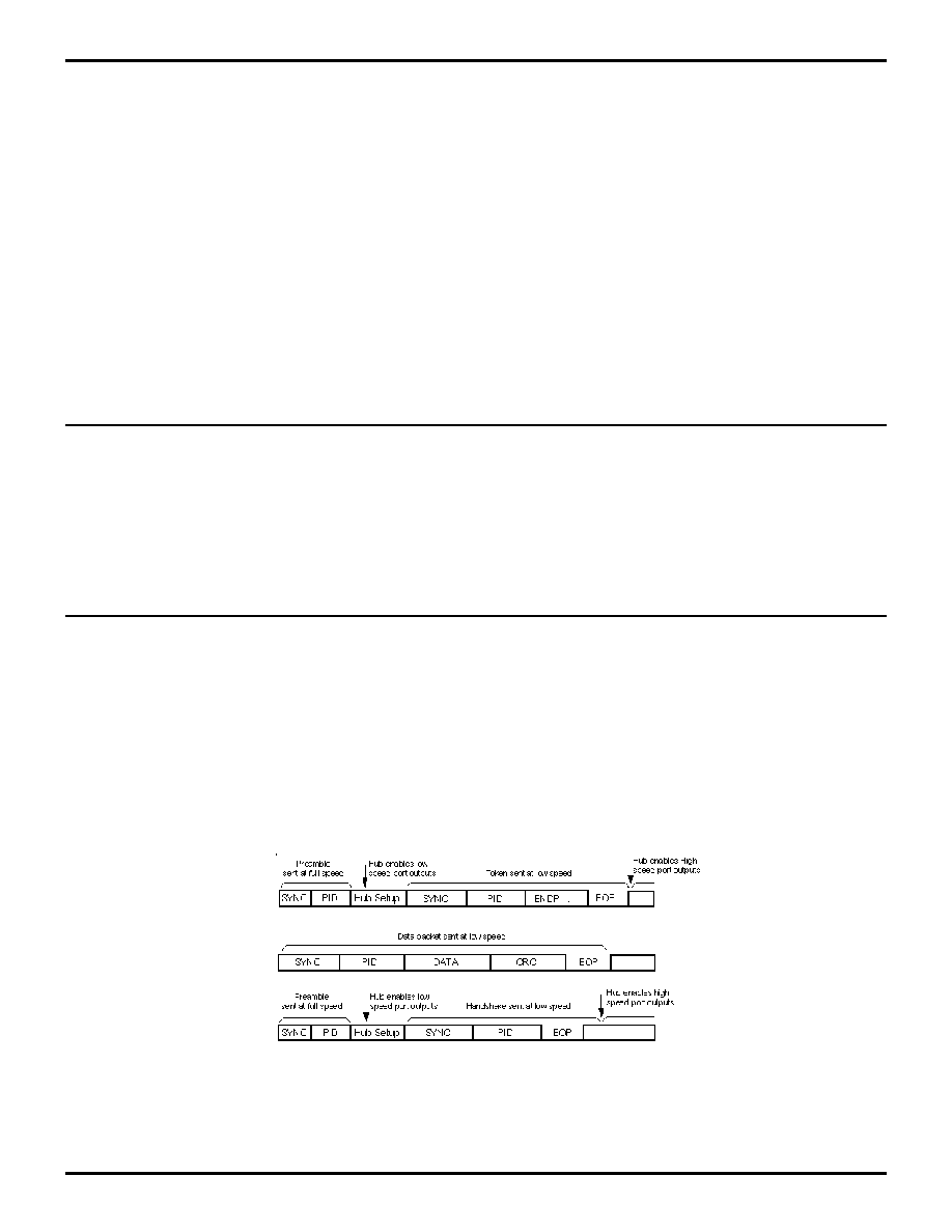
- USB Mode. The Z8E520 includes two bidirectional en...
- Suspend is dedicated through firmware by timing th...
- In Stop Mode, with the WDT disabled, power require...
- In Stop Mode, with the WDT enabled, slightly more ...
- The USB portion of the chip is divided into two ar...
- The SIE performs all other processing on incoming ...
- The USB SIE handles three endpoints (control at En...
- PIN IDENTIFICATION
- STANDARD Mode
- Pin #
- Symbol
- Function
- Direction
- EPROM PROGRAMMING Mode
- Pin #
- Symbol
- Function
- Direction
- ABSOLUTE MAXIMUM RATINGS
- Stresses greater than those listed under Absolute ...
- Parameter
- Min
- Max
- Units
- Note
- Ambient Temperature under Bias
- Storage Temperature
- Voltage on any Pin with Respect to VSS
- Voltage on VDD Pin with Respect to VSS
- Total Power Dissipation
- Maximum Allowable Current out of VSS
- Maximum Allowable Current into VDD
- Maximum Allowable Current into an Input Pin
- Maximum Allowable Current into an Open-Drain Pin
- Maximum Allowable Sink Output Current by Any I/O P...
- Maximum Allowable Source Output Current by Any I/O...
- Maximum Allowable Sink Output Current by Port A
- Maximum Allowable Source Output Current by Port A
- Maximum Allowable Sink Output Current by Port B
- Maximum Allowable Source Output Current by Port B
- STANDARD TEST CONDITIONS
- The characteristics listed here apply for standard...
- TA = 25∞C; VCC = GND = 0V; f = 1.0 MHz; unmeasured...
- Parameter
- Max
- Note:� Frequency tolerance ±10%
- DC CHARACTERISTICS: USB Mode
- TA = 0∞C to +70∞C
- Sym
- Parameter
- VCC
- Min
- Max
- Units
- Conditions
- Notes
- VCH
- Clock Input High
- Voltage
- Driven by External
- Clock Generator
- VCL
- Clock Input Low
- Voltage
- Driven by External
- Clock Generator
- VIH
- Input High Voltage
- VIL
- Input Low Voltage
- VOH
- Output High Voltage
- (Port A, B)
- IOH = Ö2.0 mA
- VOL1
- Output Low Voltage
- (Port A, B)
- IOL = +4.0 mA
- VOL2
- Output Low Voltage
- (Port A, B)
- IOL = +6 mA,
- VOFFSET
- Comparator Input Offset Voltage
- IIL
- Input Leakage
- VIN = 0V, VCC
- IOL
- Output Leakage
- VIN = 0V, VCC
- VICR
- Comparator Input
- Common Mode
- Voltage Range
- ICC
- Supply Current
- @ 6 MHz (Internal open drain)
- ICC1
- HALT Mode
- @ 6 MHz (no CPU; RC/WDT & Detect; D+/DÖ; I/O activ...
- ICC2
- Stop Current
- ICC3
- Stop Current w/o RC/WDT
- D+, DÖ
- Differential Signaling
- @ >200 mV Difference
- DC CHARACTERISTICS: ps/2 Mode
- Vcc = 4.5V Ö 5.5V
- TA = 0∞C to +70∞C
- Sym
- Parameter
- VCC
- Min
- Max
- Units
- Conditions
- Notes
- VCH
- Clock Input High
- Voltage
- Driven by External
- Clock Generator
- VCL
- Clock Input Low
- Voltage
- Driven by External
- Clock Generator
- VIH
- Input High Voltage
- VIL
- Input Low Voltage
- VOH
- Output High Voltage
- IOH = Ö2.0 mA
- VOL1
- Output Low Voltage
- IOL = +4.0 mA
- VOL2
- Output Low Voltage
- IOL = +6 mA,
- VOFFSET
- Comparator Input Offset Voltage
- IIL
- Input Leakage
- VIN = 0V, VCC
- IOL
- Output Leakage
- VIN = 0V, VCC
- VICR
- Comparator Input
- Common Mode
- Voltage Range
- ICC
- Supply Current
- @ 6 MHz
- ICC1
- HALT Current
- @ 6 MHz (no CPU; no SIE)
- ICC2
- Stop Current
- ICC3
- Stop Current w/o RC/WDT
- DC CHARACTERISTICS: RS232 Mode
- Vcc = 4.0V Ö 6.0V
- TA = 0∞C to +70∞C
- Sym
- Parameter
- VCC
- Min
- Max
- Units
- Conditions
- Notes
- VCH
- Clock Input High
- Voltage
- Driven by External
- Clock Generator
- VCL
- Clock Input Low
- Voltage
- Driven by External
- Clock Generator
- VIH
- Input High Voltage
- VIL
- Input Low Voltage
- VOH
- Output High Voltage
- IOH = Ö2.0 mA
- VOL1
- Output Low Voltage
- IOL = +4.0 mA
- VOL2
- Output Low Voltage
- IOL = +6 mA,
- VOFFSET
- Comparator Input Offset Voltage
- IIL
- Input Leakage
- VIN = 0V, VCC
- IOL
- Output Leakage
- VIN = 0V, VCC
- VICR
- Comparator Input
- Common Mode
- Voltage Range
- ICC
- Supply Current
- @ 3 MHz (6 MHz/2)
- ICC1
- HALT Mode
- @ 3 MHz
- ICC2
- Stop Current
- ICC3
- Stop Current w/o RC/WDT
- DC CHARACTERISTICS: I/O Mode
- Vcc = 4.0V Ö 6.0V
- TA = 0∞C to +70∞C
- Sym
- Parameter
- VCC
- Min
- Max
- Units
- Conditions
- Notes
- VCH
- Clock Input High
- Voltage
- Driven by External
- Clock Generator
- VCL
- Clock Input Low
- Voltage
- Driven by External
- Clock Generator
- VIH
- Input High Voltage
- VIL
- Input Low Voltage
- VOH
- Output High Voltage
- IOH = Ö2.0 mA
- VOL1
- Output Low Voltage
- IOL = +4.0 mA
- VOL2
- Output Low Voltage
- IOL = +6 mA,
- VOFFSET
- Comparator Input Offset Voltage
- IIL
- Input Leakage
- VIN = 0V, VCC
- IOL
- Output Leakage
- VIN = 0V, VCC
- VICR
- Comparator Input
- Common Mode
- Voltage Range
- ICC
- Supply Current
- @ 6 MHz
- ICCA
- @ 5.5V
- ICCB
- @ 6.0V (6 MHz/2)
- ICC1
- HALT w/ RC and WDT
- ICC2
- AC electrical characteristics
- TA = 0∞C to +70∞C
- 6 MHz
- No
- Symbol
- Parameter
- Min
- Max
- Units
- Notes
- 1
- 2
- 3
- 4
- 5
- 6
- 7
- 8
- 9
- 10
- 11
- 12
- 13
- 3
- 14
- POR
- Power supply; POR rate/Volt level
- 15
- TrC
- RC Clock Period (internal)
- Pin Functions
- Port A. Port A (4Ö7) includes a Sink configuration...
- In Sink, the options include input wakeup, bidirec...
- In Switch, the options also include input wakeup, ...
- Symbol
- Parameter
- Min.
- Max.
- Units
- Conditions
- N
- Number of Bits
- Bits
- 4 bits, 16 settings, 0Ö15 mA
- DNL
- Diff Non-Linearity
- 0.50
- LSB
- I0
- Zero Code/Disable
- A
- Disabled
- ILSB
- LSB Current
- 0.65
- 1.35
- mA
- 35%
- IF
- Full Scale Current
- 9.75
- 20.25
- mA
- 35%, Note 1
- Tsettle
- Settling Time
- 1600
- nS
- Within 10% of final value
- Iovershoot
- Overshoot Current
- 1.05*Iset
- A
- Vcomp
- Compliance Voltage
- 1.1
- V
- Above Vss with IFMAX
- Port B. Port B (0Ö5) includes a Quadrature configu...
- Symbol
- Parameter
- Min.
- Max.
- Units
- Conditions
- VR1
- Voltage Reference 1
- VR2
- Voltage Reference 2
- VR3
- Voltage Reference 3
- Ratio
- Ratio Accuracy
- Note (1)
- Comp EnableÑBit D7
- VREFÑ Bits D5:4
- Selected
- Conditions
- Symbol
- Parameter
- Min.
- Max.
- Units
- Conditions
- VMID
- Midpoint Voltage
- RL1
- Load Resistor 1
- Pad to VSS, track RL2, RL3
- RL2
- Load Resistor 2
- Pad to VSS, track RL1, RL3
- RL3
- Load Resistor 3
- Pad to VSS, track RL1, RL2
- RL4
- Load Resistor 4
- Pad to VCC
- RL5
- Load Resistor 5
- Pad to VCC
- RL6
- Load Resistor 6
- Pad to VCC
- Ratio
- Ratio Accuracy
- Note (1)
- Divider Bits D2:0
- Load Selected to VSS
- Load Selected to VCC
- Symbol
- Parameter
- Min.
- Max.
- Units
- Conditions
- VOS
- Offset Voltage
- HYS
- Hysteresis
- Common Mode, Note (1)
- VCM
- Voltage Range
- Trf
- Response Time Fast
- 700 mV/µs with 25 mV overdrive
- Trs
- Response Time Slow
- 15 mV/µs with 25 mV overdrive
- IDD
- Supply Current
- Port B. Port B (6Ö7) is configured as a serial com...
- USB
- PS/2
- RS232
- GPIO
- Port B (6) has a programmable internal pullup of 7...
- Functional Description
- Program Memory. The 16-bit program counter address...
- The first 14 bytes of program memory are reserved ...
- Register File. The register file consists of the f...
- EP Mode
- Description
- Buffer Address
- 0x88Ö0x8F
- 0x98Ö0x9F
- 0xA8Ö0xAF
- EP1 OFF, EP2 OFF
- EP1 IN, EP2 OFF
- EP1 OUT, EP2 OFF
- EP1 CONTROL
- EP1 OUT, EP2 OUT
- EP1 IN, EP1 OUT
- EP1 OUT, EP1 IN
- EP1 IN, EP2 IN
- Communication register definitions (usb mode)
- The following definitions on pages 23Ö26 describe ...
- PORT A, PORT B: I/O Port data registers. At all ti...
- ADDR: Determines the USB Device Address. Cleared b...
- SIE MODE: Determines the mode of the SIE communica...
- SIE Mode
- Description
- Port B7
- Port B6
- GPIO: The SIE is off and the communication lines a...
- USB: Port B7 is D+, which connects to pin 3 on a s...
- PS/2: Port B7 is CLOCK, which connects to pin 5 on...
- RS232: Port B7 is serial data out (T x D). Port B6...
- SIE POWER: Powers up the SIE when USB Resume signa...
- FORCE RESUME: Forces a K state on the USB pins. Re...
- ACTIVITY: This bit is set by the SIE when the stat...
- J STATE: This bit is set when the USB is in the èJ...
- EP MODE: These bits define the operation of the no...
- EP Mode
- Description
- LOW PRIORITY INTR: This register contains the IRQ ...
- LOW PRIORITY MASK: This register contains mask bit...
- Table 10 illustrates both Low Priority MASK and IN...
- EP
- MODE
- Description
- EP
- 2
- EP
- 1
- EP
- 0
- IN DONE: The SIE received a valid IN token, sent t...
- IN NAK SENT: The SIE sent a NAK on an IN transmiss...
- OUT PACKET READY: The SIE received a valid OUT pac...
- OUT NAK SENT: The SIE sent a NAK on an OUT transac...
- HIGH PRIORITY INTR: This register contains the IRQ...
- RESUME: This bit is set when the ACTIVITY bit is s...
- STALL SENT EP2: This bit is set when a STALL is se...
- STALL SENT EP1: This bit is set when a STALL is se...
- STALL SENT EP0: This bit is set when a STALL is se...
- SETUP EP1: This bit is set after the completion of...
- SETUP EP0: This bit is set after the completion of...
- HIGH PRIORITY MASK: This register contains mask bi...
- EP0 CSR: Control/Status register of Endpoint 0 (Co...
- EP1/2 CSR: Control/Status register of additional e...
- Table 11 illustrates the EP1/2 CSR registers accor...
- EP
- MODE
- Description
- EP
- 1
- FORCE STALL: Forces the SIE to stall all IN and OU...
- IN PACKET READY: When clear, IN transactions are N...
- FORCE NAK: Setting this bit clears IN PACKET READY...
- IN DATA TOGGLE: Indicates what type of PID to use ...
- OUT SERVICED: When cleared, OUT transactions are N...
- OUT DATA TOGGLE: Indicates what type of PID was re...
- SETUP BUFFER VOLATILE: Indicates that the SIE has ...
- ACK STATUS OUT: This bit serves to filter the resp...
- While ACK STATUS OUT is set:
- If IN NAK SENT is clear, the SIE will ACK an empty...
- If IN NAK SENT is set, the SIE will NAK an empty O...
- Any other kind of OUT transaction will be stalled ...
- Any out transaction will cause the SIE to set FORC...
- The successful receipt of a setup token sets FORCE...
- EP0 COUNT: Contains counts of bytes in the endpoin...
- EP1/2 COUNT: Contains counts of bytes in the endpo...
- EP MODE
- Description
- EP1/2
- COUNT
- EP OUT COUNT: Set by the SIE to indicate the numbe...
- EP IN COUNT: Set by firmware to indicate the numbe...
- Communication register definitions (Non-usb modes)...
- The following definitions describe in detail the s...
- PORT A, PORT B: Same as USB mode. Port B6 and B7 a...
- SIE MODE: Same as USB mode.
- LOW PRIORITY INTR: This register contains the IRQ ...
- LOW PRIORITY MASK: This register contains mask bit...
- XMIT COMM ERROR: Indicates that a communications e...
- XMIT DONE: Indicates that XMIT PACKET SIZE bytes h...
- HIGH PRIORITY INTR: This register contains the IRQ...
- HIGH PRIORITY MASK: This register contains mask bi...
- OVERRUN ERROR: Indicates that RCV READY was clear ...
- RCV COMM ERROR: Indicates that a communications er...
- RCV DONE: Indicates that RCV PACKET SIZE bytes hav...
- COMM CSR: Controls the SIE in PS/2 and RS232-C mod...
- XMIT READY: Indicates to the SIE that the XMIT buf...
- RCV READY: Indicates to the SIE that the most rece...
- RCV PACKET SIZE: Number of bytes to receive before...
- XMIT PACKET SIZE: The number of bytes to send befo...
- LAST BYTE RECEIVED OFFSET: Indicates the offset in...
- NEXT SEND BYTE OFFSET: Indicates the offset in the...
- Initial States: COMM REGISTERS, UPON CHANGING MODE...
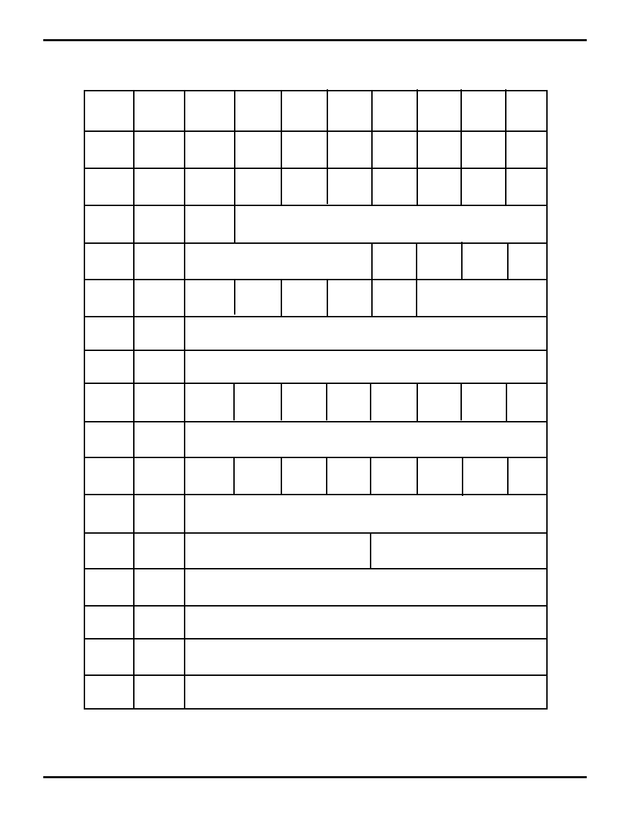
- ADDR
- NAME
- D7
- D6
- D5
- D4
- D3
- D2
- D1
- D0
- All Registers in this state are cleared to 0 on PO...
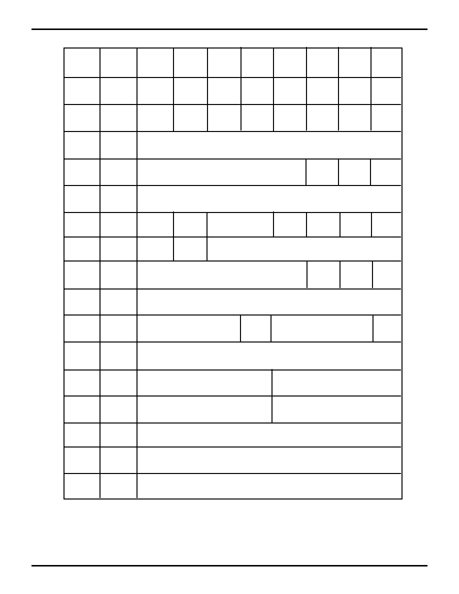
- Port configuration registers
- PORT register definitions
- The following definitions describe in detail the s...
- WAKE: When set, this pin is capable of waking the ...
- PUSH/PULL: When set, this pin is a push-pull outpu...
- PULLUP ON: When set, the pull-up resistor is on.
- OUTPUT: When set, the pinês output drivers are ena...
- SINK: Indicates the level of current drawn by the ...
- DIVIDER: Selects one of the three voltage dividers...
- VREF: Indicates the voltage reference level for th...
- COMP ENABLE: When set, the comparator is powered. ...
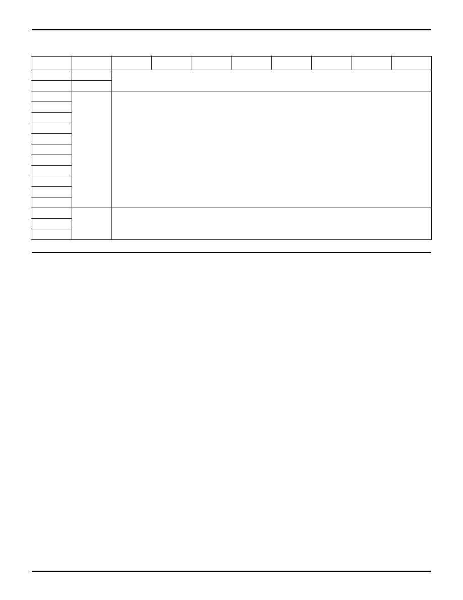
- Counter/Timers. For the Z8E20, 8-bit timers T0 and...
- Each 8-bit timer is provided a pair of registers, ...
- Software is allowed to write to any register at an...
- Similarly, if software updates the initialization ...
- If a timer pair is defined to operate as a single ...
- In parallel with the posting of the interrupt requ...
- Note:� Any time that a timer pair is defined to ac...
- If interrupts are disabled for a long period of ti...
- If T0 and T1 are defined to work independently, th...
- When T01 is enabled, it can use a pair of 16-bit a...
- To use the cascaded timers as a PWM, one must init...
- After the auto-initialization has been completed, ...
- Watch-Dog Timer. The WDT can be programmed at anyt...
- Default value (Reset) = 98 ms
- The RC oscillator is under firmware control. If th...
- WDT Control Registers. Select time-out values for ...
- Interrupts. The Z8E520 has six different interrupt...
- Priority
- IRQ
- .
- When more than one interrupt is pending, prioritie...
- EMI. Lower EMI on the Z8E520 is achieved through c...
- The Z8E520 also accepts external clock from XTAL I...
- Power-On-Reset (POR). A timer circuit is triggered...
- The POR timer circuit is a one-shot timer triggere...
- HALT. HALT turns off the internal CPU clock, but n...
- USB Reset. Detection by the SIE of a reset from th...
- VBO Circuit. The Voltage Brown Out circuit will de...
- STOP. This instruction turns off the internal cloc...
- Note:� The timer cannot generate an interrupt in S...
- The interrupt causes the processor to restart the ...
- Z8Plus System registers
- The registers displayed in Figures 21Ö27 represent...
- Package information
- Ordering information
- 6 MHz
- 6 MHz
- 20-Pin DIP
- 20-Pin SOIC
- For fast results, contact your Zilog sales office ...
- P = Plastic DIP V = Plastic Leaded Chip Carrier F ...
- 06 = 6 MHz
- C = Plastic Standard
- S = 0∞C to +70∞C
- Customer is cautioned that while reasonable effort...
- The product represented by this CPS is newly intro...
- Customer is advised that this product does not mee...
- 1998 by Zilog, Inc. All rights reserved. No part...
- Zilog, Inc. makes no warranty, express, statutory,...
- Zilog, Inc. shall not be responsible for any error...
- Zilogês products are not authorized for use as cri...
- Zilog, Inc. 210 East Hacienda Ave.
- Campbell, CA 95008-6600
- Telephone (408) 370-8000
- FAX 408 370-8056
- Internet: http://www.zilog.com

DS97KEY2005
P R E L I M I N A R Y
1
P
RELIMINARY
P
RODUCT
S
PECIFICATION
Z8E520/C520
1
1.5 MBPS USB L
OW
-P
OWER
D
EVICE
C
ONTROLLER
F
OR
M
ULTIPROTOCOL
P
OINTING
D
EVICES
FEATURES
s
Six Vectored Interrupts with Fixed Priority
s
Processor Speed Dividable by Firmware Control
s
Operating Current: 5 mA typical in USB Mode; 2.5 mA
typical in Serial Mode (@ 3 MHz); 5 mA typical in PS/2
Mode
s
16 Total Input/Output Pins (Open-Drain/Push-Pull)
Configurable
s
6 inputs with 3 level Programmable Reference
Comparators
s
16-Bit Programmable Watch-Dog Timer (WDT) with
Internal RC Oscillator
s
Software Programmable Timers Configurable as:
≠
Two 8-Bit Standard Timers and One 16-Bit
Standard Timer or
≠
One 16-Bit Standard Timer and One 16-Bit Pulse
Width Modulator (PWM) Timer
s
Identical Masked ROM Version (Z8C520)
s
On-Chip Oscillator that accepts a Ceramic Resonator or
External Clock
s
Hardware Support for PS/2, Serial, USB, and General-
Purpose I/O (GPIO)
s
Power Reduction Modes:
≠
STOP Mode (functionality shut down except SMR)
≠
HALT Mode (XTAL still running-peripherals active)
s
USB SIE Compliant with USB Spec 1.0
s
4.0 VDC to 6.0 VDC Operating Range @ 0
∞
C to +70
∞
C
GENERAL DESCRIPTION
Zilog's Z8E520 (OTP) and Z8C520 (Masked ROM) micro-
controllers are low-power Z8
Plus
MCUs, designed for the
cost-effective implementation of USB and multiprotocol
pointing devices.
For applications demanding powerful I/O capabilities, the
Z8E520's input and output lines are grouped into two ports,
and are configurable under software control to provide tim-
ing, status signals, or parallel I/O.
Both 8-bit and 16-bit timers, with a large number of user se-
lectable modes, off-load the system of administering real-
time tasks such as counting/timing and I/O data communi-
cations.
The microcontroller clock frequency is derived from the
system clock by a programmable divider under firmware
control.
The device is capable of functioning in four distinct, select-
able communications modes: PS/2, RS232, GPIO (Gener-
al-purpose I/O), and USB. The communications mode de-
termines the functionality of the two special serial
communications pins (PB6 and PB7). The device is placed
in the required mode when firmware sets the specified
mode bit in the communications control register. The firm-
ware interface is similar in all modes. The same buffer area
in RAM will accept the data to be transmitted. Up to 8 bytes
may be loaded, and the data will actually be transmitted as
soon as the appropriate command is issued (setting In
Packet Ready in USB mode, for example).
Part
ROM
RAM
Speed
Number
(KB)
(Bytes)
(MHz)
Z8E520 (OTP)
6
176
12
Z8C520 (ROM)
6
176
12

Z8E520/C520
1.5 MBPS USB Device Controller
Zilog
2
P R E L I M I N A R Y
DS97KEY2005
GENERAL DESCRIPTION
(Continued)
Power connections follow conventional descriptions at
right:
Connection
Circuit
Device
Power
V
CC
V
DD
Ground
GND
V
SS
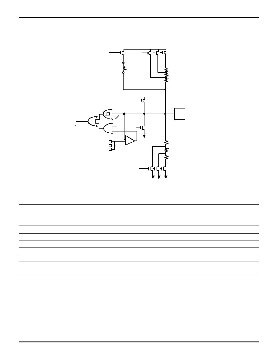
Figure 1. Z8E520 Functional Block Diagram
One 16-bit
Std. Timer
Interrupt
Control
6 Analog
Comparators
ALU
FLAG
Register
Pointer
RAM
Register File
(160 Bytes)
Machine Timing
& Inst. Control
6 K Bytes
Prg. Memory
Program
Counter
V
CC
GND
Ceramic Resonator
Port A
Port B
I/O
Two 8-bit Timers
or
One 16-bit PWM
Timer
I/O
ZIE
WDT
RC OSC
INTERNAL
Port B
(6≠7)
Z8E520/C520
Zilog
1.5 MBPS USB Device Controller
DS97KEY2005
P R E L I M I N A R Y
3
1
COMMUNICATION MODES
The Z8E520/C520 allows its user to function in a variety of
communication modes. Having this freedom within a sin-
gle chip opens up many possibilities when utilizing multiple
protocol applications. The modes incorporated into the
Z8E520/C520 include PS/2, RS232, GPIO, and USB. A
description of each mode is detailed below.
PS/2 Mode
. The serial baud rate is fixed at 12.5 K baud.
Received data is automatically checked for parity and
framing errors while HOST abort is supported. The serial
communications pins function as PS/2 compatible DATA
(PB6) and CLOCK (PB7).
RS232 Mode.
The data rate is fixed at 1200 baud. The se-
rial communications pins function as RxD (PB6) and TxD
(PB7).
GPIO Mode
. In General-Purpose I/O Mode, the serial
communications pins function as standard I/O pins, with
Input, Output P/P (Push/Pull) and OD (Open Drain) Out-
put.
USB Mode
. The Z8E520 includes two bidirectional end-
points that support communications compliant to the USB
Specification version 1.0. The serial communications pins
function as D≠ (PB6) and D+ (PB7). The detailed behavior
of the SIE is controllable by the firmware, and three sepa-
rate power states are provided for USB Suspend Mode
support (see section below).
USB SUSPEND/RESUME FUNCTIONALITY
Suspend is dedicated through firmware by timing the Ac-
tivity bit which is set by the SIE.
In Stop Mode, with the WDT disabled, power requirements
are minimized. No power is consumed by the voltage reg-
ulator, the Z8
Plus
core, nor differential detector. Only the
Stop Mode Recovery (SMR) is enabled, so an input signal
or Resume from the host can be detected and used to
wake up the microcontroller.
In Stop Mode, with the WDT enabled, slightly more power
is consumed, but the device can wake up periodically to
perform maintenance and detect a change of state in the
application.
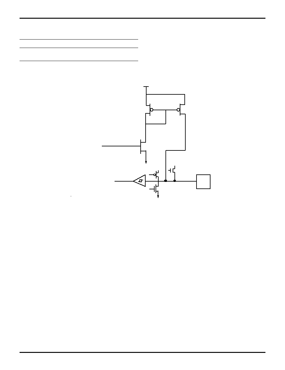
USB FUNCTIONAL BLOCK DESCRIPTION
The USB portion of the chip is divided into two areas, the
transceiver and the Serial Interface Engine (SIE). The
transceiver handles incoming differential signals and "sin-
gle ended zero (SE0)". It also converts output data in digi-
tal form to differential drive at the proper levels (Figure 2).
The SIE performs all other processing on incoming and out
going data, including signal recovery timing, bit stuffing,
validity checking, data sequencing, and handshaking to
the host. Data flow into and out of the MCU portions are
dedicated registers mapped into Expanded Register File
Memory.
The USB SIE handles three endpoints (control at Endpoint
0, data into the host from Endpoint 1 and data out from the
host as Endpoint 2). All communications are at the
1.5 MB/sec data rate. Endpoint 1 and 2 can be combined
as Control EP1.
Figure 2. Data To/From Z8E520/C520

Z8E520/C520
1.5 MBPS USB Device Controller
Zilog
4
P R E L I M I N A R Y
DS97KEY2005
PIN IDENTIFICATION
Figure 3. 20-Pin DIP/SOIC Pin Assignments
PA6
PA7
PB0
PB1
PB2
PB3
PB4
PB5
PA0
PA1
PA5
PA4
XTAL (2)
GND
XTAL (1)
VCC
PB7
PB6
PA3
PA2
20
20-Pin
DIP/SOIC
1
10
11
Table 1. 20-Pin DIP/SOIC Pin Identification
STANDARD Mode
Pin #
Symbol
Function
Direction
1, 2
PA X(6,7)
Digital I/O + I SINK
Bidirectional
3≠8
PB X(0≠5)
Digital I/O +Comparators
Bidirectional
9≠12
PA X(0≠3)
Digital I/O
Bidirectional
13≠14
PB X (6≠7)
Digital I/O + Communications
Bidirectional
15
V
cc
Power
16
XTAL (1)
Clock
17
GND
Power
18
XTAL (2)
Clock
19, 20
PA X(4,5)
Digital I/O + I SINK
Bidirectional

Z8E520/C520
Zilog
1.5 MBPS USB Device Controller
DS97KEY2005
P R E L I M I N A R Y
5
1
Figure 4. 20-Pin DIP/SOIC Pin Assignments:
EPROM Programming Mode
D0
D1
D2
D3
D4
D5
D6
D7
TST_CLR
PGM
CLK (1 MHz)
GND
(CLK OUT)
VCC
VPP
ADDRCLK
20
20-Pin
DIP/SOIC
1
10
11
Table 2. 20-Pin DIP/SOIC Pin Identification:
EPROM Programming Mode
EPROM PROGRAMMING Mode
Pin #
Symbol
Function
Direction
1≠8
D0≠D7
Data Bus
I/O
9
TST_CLR
Reset Internal Address Counter
In
10
PGM
Program Pin
In
11
ADDRCLK
Clock to Address Counter
In
12
V
PP
High Voltage to Program Device
Power
13≠14
Unused
15
V
CC
Power
Power
16
CLKOUT
Output from Clock Inverter
Out
17
GND
Power Ref
Power
18
CLK
1 MHz to chip
In
19
Unused
20
Unused

Z8E520/C520
1.5 MBPS USB Device Controller
Zilog
6
P R E L I M I N A R Y
DS97KEY2005
ABSOLUTE MAXIMUM RATINGS
Stresses greater than those listed under Absolute Maxi-
mum Ratings may cause permanent damage to the de-
vice. This rating is a stress rating only; functional operation
of the device at any condition above those indicated in the
operational sections of these specifications is not implied.
Exposure to absolute maximum rating conditions for an
extended period may affect device reliability. Total power
dissipation should not exceed 880 mW for the package.
Power dissipation is calculated as follows:
Total Power Dissipation =
V
DD
x [I
DD
≠ (sum of I
OH
)]
+ sum of [(V
DD
≠ V
OH
) x I
OH
]
+ sum of (V
0L
x I
0L
)
Parameter
Min
Max
Units
Note
Ambient Temperature under Bias
≠40
+105
C
Storage Temperature
≠65
+150
C
Voltage on any Pin with Respect to V
SS
≠0.6
+7
V
Voltage on V
DD
Pin with Respect to V
SS
≠0.3
+7
V
Total Power Dissipation
880
mW
Maximum Allowable Current out of V
SS
80
mA
Maximum Allowable Current into V
DD
80
mA
Maximum Allowable Current into an Input Pin
≠600
+600
µ
A
1
Maximum Allowable Current into an Open-Drain Pin
≠600
+600
µ
A
2
Maximum Allowable Sink Output Current by Any I/O Pin
25
mA
Maximum Allowable Source Output Current by Any I/O Pin
25
mA
Maximum Allowable Sink Output Current by Port A
40
mA
Maximum Allowable Source Output Current by Port A
40
mA
Maximum Allowable Sink Output Current by Port B
40
mA
Maximum Allowable Source Output Current by Port B
40
mA
Notes:
1. Excludes XTAL pins.
2. Device pin is not at an output Low state.
Z8E520/C520
Zilog
1.5 MBPS USB Device Controller
DS97KEY2005
P R E L I M I N A R Y
7
1
STANDARD TEST CONDITIONS
The characteristics listed here apply for standard test con-
ditions as noted. All voltages are referenced to GND. Pos-
itive current flows into the referenced pin (Figure 5).
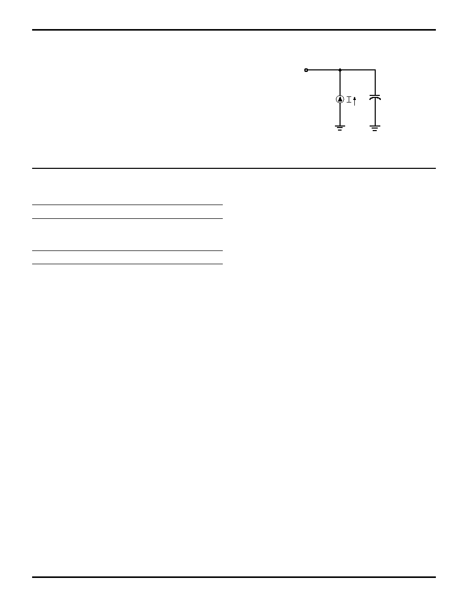
CAPACITANCE
T
A
= 25
∞
C; V
CC
= GND = 0V; f = 1.0 MHz; unmeasured pins returned to GND.
Figure 5. Test Load Diagram
From Output
Under Test
150 pF
Parameter
Max
Input Capacitance
12 pF
Output Capacitance
12 pF
I/O Capacitance
12 pF
Note:
Frequency tolerance
±
10%

Z8E520/C520
1.5 MBPS USB Device Controller
Zilog
8
P R E L I M I N A R Y
DS97KEY2005
DC CHARACTERISTICS: USB MODE
V
cc
= 4.4V ≠ 5.25V
T
A
= 0
∞
C to +70
∞
C
Sym
Parameter
V
CC
Min
Max
Units Conditions
Notes
V
CH
Clock Input High
Voltage
0.7V
CC
V
CC
+0.3
V
Driven by External
Clock Generator
V
CL
Clock Input Low
Voltage
V
SS
≠0.3
0.2V
CC
V
Driven by External
Clock Generator
V
IH
Input High Voltage
0.7V
CC
V
CC
+0.3
V
V
IL
Input Low Voltage
V
SS
≠0.3
0.2V
CC
V
V
OH
Output High Voltage
(Port A, B)
V
CC
≠0.4
V
I
OH
= ≠2.0 mA
V
OL1
Output Low Voltage
(Port A, B)
0.6
V
I
OL
= +4.0 mA
4
V
OL2
Output Low Voltage
(Port A, B)
1.2
V
I
OL
= +6 mA,
4
V
OFFSET
Comparator Input Offset
Voltage
25.0
mV
I
IL
Input Leakage
≠1.0
2.0
µ
A
V
IN
= 0V, V
CC
I
OL
Output Leakage
≠1.0
2.0
µ
A
V
IN
= 0V, V
CC
V
ICR
Comparator Input
Common Mode
Voltage Range
V
SS
≠0.3
V
CC
≠1.0
V
I
CC
Supply Current
6.0V
5.25
6.0
mA
@ 6 MHz (Internal open
drain)
1,2
I
CC1
HALT Mode
6.0V
3.5
mA
@ 6 MHz (no CPU; RC/WDT
& Detect; D+/D≠; I/O active)
1,2
I
CC2
Stop Current
60
µ
A
I
CC3
Stop Current w/o RC/WDT
40
µ
A
D+, D≠
Differential Signaling
D≠ > D+
D+ > D≠
mV
@ >200 mV Difference
3
Notes:
1. All outputs unloaded, I/O pins floating, and all inputs are at V
CC
or V
SS
level.
2. CL1 = CL2 = 22 pF
3. Except for SE0 for EOP and Reset (see 7.1.4 of USB Specification)
4. General-Purpose I/O Mode.

Z8E520/C520
Zilog
1.5 MBPS USB Device Controller
DS97KEY2005
P R E L I M I N A R Y
9
1
DC CHARACTERISTICS: PS/2 MODE
V
cc
= 4.5V ≠ 5.5V
T
A
= 0
∞
C to +70
∞
C
Sym
Parameter
V
CC
Min
Max
Units Conditions
Notes
V
CH
Clock Input High
Voltage
0.7V
CC
V
CC
+0.3
V
Driven by External
Clock Generator
V
CL
Clock Input Low
Voltage
V
SS
≠0.3
0.2V
CC
V
Driven by External
Clock Generator
V
IH
Input High Voltage
0.7V
CC
V
CC
+0.3
V
V
IL
Input Low Voltage
V
SS
≠0.3
0.2V
CC
V
V
OH
Output High Voltage
V
CC
≠0.4
V
I
OH
= ≠2.0 mA
V
OL1
Output Low Voltage
0.6
V
I
OL
= +4.0 mA
V
OL2
Output Low Voltage
1.2
V
I
OL
= +6 mA,
V
OFFSET
Comparator Input Offset
Voltage
25.0
mV
I
IL
Input Leakage
≠1.0
2.0
µ
A
V
IN
= 0V, V
CC
I
OL
Output Leakage
≠1.0
2.0
µ
A
V
IN
= 0V, V
CC
V
ICR
Comparator Input
Common Mode
Voltage Range
V
SS
≠0.3
V
CC
≠1.0
V
I
CC
Supply Current
5.5V
6.0
mA
@ 6 MHz
1,2
I
CC1
HALT Current
5.5V
3.5
mA
@ 6 MHz (no CPU; no SIE)
1,2
I
CC2
Stop Current
60
µ
A
I
CC3
Stop Current w/o RC/WDT
40
µ
A
Notes:
1. All outputs unloaded, I/O pins floating, and all inputs are at V
CC
or V
SS
level.
2. CL1 = CL2 = 22 pF.

Z8E520/C520
1.5 MBPS USB Device Controller
Zilog
10
P R E L I M I N A R Y
DS97KEY2005
DC CHARACTERISTICS: RS232 MODE
V
cc
= 4.0V ≠ 6.0V
T
A
= 0
∞
C to +70
∞
C
Sym
Parameter
V
CC
Min
Max
Units Conditions
Notes
V
CH
Clock Input High
Voltage
0.7V
CC
V
CC
+0.3
V
Driven by External
Clock Generator
V
CL
Clock Input Low
Voltage
V
SS
≠0.3
0.2V
CC
V
Driven by External
Clock Generator
V
IH
Input High Voltage
0.7V
CC
V
CC
+0.3
V
V
IL
Input Low Voltage
V
SS
≠0.3
0.2V
CC
V
V
OH
Output High Voltage
V
CC
≠0.4
V
I
OH
= ≠2.0 mA
V
OL1
Output Low Voltage
0.6
V
I
OL
= +4.0 mA
V
OL2
Output Low Voltage
1.2
V
I
OL
= +6 mA,
V
OFFSET
Comparator Input Offset
Voltage
25.0
mV
I
IL
Input Leakage
≠1.0
2.0
µ
A
V
IN
= 0V, V
CC
I
OL
Output Leakage
≠1.0
2.0
µ
A
V
IN
= 0V, V
CC
V
ICR
Comparator Input
Common Mode
Voltage Range
V
SS
≠0.3 V
CC
≠1.0
V
I
CC
Supply Current
6.0V
4.0
mA
@ 3 MHz (6 MHz/2)
1,2
I
CC1
HALT Mode
6.0V
3.5
mA
@ 3 MHz
1,2
I
CC2
Stop Current
60
µ
A
I
CC3
Stop Current w/o
RC/WDT
40
µ
A
Notes:
1. All outputs unloaded, I/O pins floating, and all inputs are at V
CC
or V
SS
level.
2. CL1 = CL2 = 22 pF.

Z8E520/C520
Zilog
1.5 MBPS USB Device Controller
DS97KEY2005
P R E L I M I N A R Y
11
1
DC CHARACTERISTICS: I/O MODE
V
cc
= 4.0V ≠ 6.0V
T
A
= 0
∞
C to +70
∞
C
Sym
Parameter
V
CC
Min
Max
Units Conditions
Notes
V
CH
Clock Input High
Voltage
0.7V
CC
V
CC
+0.3
V
Driven by External
Clock Generator
V
CL
Clock Input Low
Voltage
V
SS
≠0.3
0.2V
CC
V
Driven by External
Clock Generator
V
IH
Input High Voltage
0.7V
CC
V
CC
+0.3
V
V
IL
Input Low Voltage
V
SS
≠0.3
0.2V
CC
V
V
OH
Output High Voltage
V
CC
≠0.4
V
I
OH
= ≠2.0 mA
V
OL1
Output Low Voltage
0.6
V
I
OL
= +4.0 mA
V
OL2
Output Low Voltage
1.2
V
I
OL
= +6 mA,
V
OFFSET
Comparator Input Offset
Voltage
25.0
mV
I
IL
Input Leakage
≠1.0
2.0
µ
A
V
IN
= 0V, V
CC
I
OL
Output Leakage
≠1.0
2.0
µ
A
V
IN
= 0V, V
CC
V
ICR
Comparator Input
Common Mode
Voltage Range
V
SS
≠0.3
V
CC
≠1.0
V
I
CC
Supply Current
6.0V
6.0
mA
@ 6 MHz
1,2
I
CCA
5.5V
6.0
mA
@ 5.5V
1,2
I
CCB
4.0
mA
@ 6.0V (6 MHz/2)
I
CC1
HALT w/ RC and WDT
60
µ
A
I
CC2
50
µ
A
Notes:
1. All outputs unloaded, I/O pins floating, and all inputs are at V
CC
or V
SS
level.
2. CL1 = CL2 = 22 pF.
Z8E520/C520
1.5 MBPS USB Device Controller
Zilog
12
P R E L I M I N A R Y
DS97KEY2005
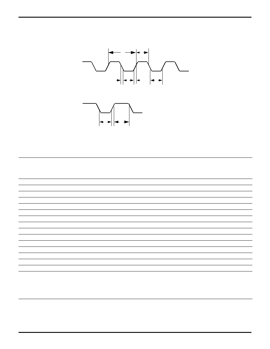
AC ELECTRICAL CHARACTERISTICS
Timing Diagram
Timing Table
Figure 6. AC Electrical Timing Diagram
1
3
3
2
2
CLOCK
IRQ
N
8
9
T
A
= 0
∞
C to +70
∞
C
6 MHz
No
Symbol
Parameter
Min
Max
Units
Notes
1
TpC
Input Clock Period
83
DC
ns
1
2
TrC,TfC
Clock Input Rise & Fall Times
5
ns
1
3
TwC
Input Clock Width
37
ns
1
4
TwTinL
Timer Input Low Width
70
ns
1
5
TwTinH
Timer Input High Width
2.5TpC
1
6
TpTin
Timer Input Period
4TpC
1
7
TrTin
Timer Input Rise & Fall Timer
100
ns
1
8
TwIL
Int. Request Low Time
70
ns
1,2
9
TwIH
Int. Request Input High Time
3TpC
1,2
10
Twsm
Stop-Mode Recovery Width Spec
100TpC
ns
11
Tost
Oscillator Start-Up Time
0.5
ms
12
Twdt
Watch-Dog Timer
1000
ms
13
D+, D≠
Differential Rise and Fall Times (USB Mode)
70
300
nS
3
14
POR
Power supply; POR rate/Volt level
15
TrC
RC Clock Period (internal)
12.5
50
µ
sec
4
Notes:
1. Timing Reference uses 0.7 V
CC
for a logic 1 and 0.2 V
CC
for a logic 0.
2. Interrupt request
3. See USB Specification 7.1.1.2
4. Corresponds to frequencies of 80 KHz to 20 KHz
Z8E520/C520
Zilog
1.5 MBPS USB Device Controller
DS97KEY2005
P R E L I M I N A R Y
13
1
PIN FUNCTIONS
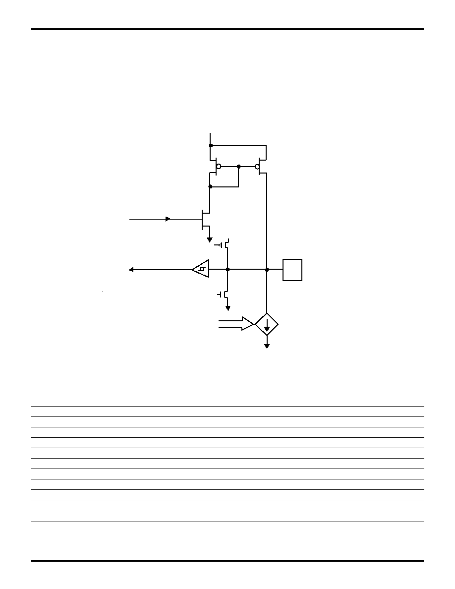
Port A. Port A (4≠7) includes a Sink configuration. Port A
(3≠0) has a Switch configuration.
In Sink, the options include input wakeup, bidirectional,
push-pull or open drain configurations (Figure 7). The Sink
is programmable from 0≠15 mA (in 1 mA increments).
In Switch, the options also include input wakeup, bidirec-
tional, push-pull or open drain configurations (Figure 8).
The only difference between the two is the programmable
Sink option.
Figure 7. Port A (4≠7) Sink Configuration
Table 3. Port A (4≠7) Programmable Current Sink Table
Symbol
Parameter
Min.
Max.
Units
Conditions
N
Number of Bits
Bits
4 bits, 16 settings, 0≠15 mA
DNL
Diff Non-Linearity
0.50
LSB
I
0
Zero Code/Disable
µ
A
Disabled
I
LSB
LSB Current
0.65
1.35
mA
35%
I
F
Full Scale Current
9.75
20.25
mA
35%, Note 1
T
settle
Settling Time
1600
nS
Within 10% of final value
I
overshoot
Overshoot Current
1.05*I
set
µ
A
V
comp
Compliance Voltage
1.1
V
Above V
ss
with I
FMAX
Notes:
1. Setting all (4) I
SNK
cells to full scale is a violation of the Absolute Maximum Rating Spec.
0 ≠15 m A/ 1 m A increm ents
Pa d
100 K
In
Vcc
V cc
Wa ke
TBD
±
30%
I
SINK
(3 :0)
Pullup Resistor Enable
Typical

Z8E520/C520
1.5 MBPS USB Device Controller
Zilog
14
P R E L I M I N A R Y
DS97KEY2005
PIN FUNCTIONS (Continued)
Figure 8. Port A (0≠3) Switch Configuration
Pad
100K
Pull-down Resistor Enable
In
Wake
Vcc
(
±
35%)
Z8E520/C520
Zilog
1.5 MBPS USB Device Controller
DS97KEY2005
P R E L I M I N A R Y
15
1
Port B. Port B (0≠5) includes a Quadrature configuration
(Figure 9), with programmable current sink and an analog
comparator with programmable reference voltages (Ta-
bles 4≠8).
PORT B (0≠5) QUADRATURE CONFIGURATION
Figure 9. Port B (0≠5) Quadrature Configuration
Table 4. Programmable Voltage Threshold
Symbol
Parameter
Min.
Max.
Units
Conditions
V
R1
Voltage Reference 1
0.21 V
CC
0.29 V
CC
V
V
R2
Voltage Reference 2
0.31 V
CC
0.39 V
CC
V
V
R3
Voltage Reference 3
0.41 V
CC
0.49 V
CC
V
Ratio
Ratio Accuracy
5
%
Note (1)
Note:
1. Greatest delta vs. specified delta.
Pad
AC
AC
Decode
V
R1
V
R3
V
R2
+ V
+V
AC = Analog Comparator Mode

Z8E520/C520
1.5 MBPS USB Device Controller
Zilog
16
P R E L I M I N A R Y
DS97KEY2005
PORT B (0≠5) QUADRATURE CONFIGURATION (Continued)
Table 5. Programmable Voltage Bit Selections (Register Addresses DA≠DF)
Comp Enable--Bit D7
V
REF
-- Bits D5:4
Selected
Conditions
0
xx
Comparator Off
Note (1)
1
01
0.25 V
CC
1
10
0.35 V
CC
1
11
0.45 V
CC
Note:
1. If all comparators are off, V
REF
can be powered off. If in Stop Mode, V
REF
is powered off.
Table 6. Programmable Load Resistor
Symbol
Parameter
Min.
Max.
Units
Conditions
V
MID
Midpoint Voltage
0.13 V
CC
0.15 V
CC
V
R
L1
Load Resistor 1
5.25
8.75
K ohm
Pad to V
SS
, track R
L2
, R
L3
R
L2
Load Resistor 2
9.00
15.00
K ohm
Pad to V
SS
, track R
L1
, R
L3
R
L3
Load Resistor 3
13.50
22.50
K ohm
Pad to V
SS
, track R
L1
, R
L2
R
L4
Load Resistor 4
32.25
53.75
K ohm
Pad to V
CC
R
L5
Load Resistor 5
55.50
92.50
K ohm
Pad to V
CC
R
L6
Load Resistor 6
83.25
138.75
K ohm
Pad to V
CC
Ratio
Ratio Accuracy
5
%
Note (1)
Note:
1. Greatest ratio vs. specified ratio.
Table 7. Programmable Load Resistor Bit Selections (Register Addresses DA≠DF
Divider Bits D2:0
Load Selected to V
SS
Load Selected to V
CC
000
No load Resistors
No load Resistors
001
7 K Selected
43 K Selected
010
12 K Selected
74 K Selected
100
18 K Selected
111 K Selected
Table 8. Comparator
Symbol
Parameter
Min.
Max.
Units
Conditions
VOS
Offset Voltage
25
mV
HYS
Hysteresis
TBD
TBD
mV
Common Mode, Note (1)
VCM
Voltage Range
V
SS
≠0.3
V
CC
≠1.0
V
T
rf
Response Time Fast
1
µ
s
700 mV/
µ
s with 25 mV overdrive
T
rs
Response Time Slow
1
µ
s
15 mV/
µ
s with 25 mV overdrive
IDD
Supply Current
100
µ
A
Note:
1. Zilog will provide specification.
Z8E520/C520
Zilog
1.5 MBPS USB Device Controller
DS97KEY2005
P R E L I M I N A R Y
17
1
Port B. Port B (6≠7) is configured as a serial communica-
tion port as follows:
Port B (6) has a programmable internal pullup of 7.5 K
±
30%. For USB Mode, Port B (7) requires an external pullup
of 7.5 K
±
1% to V
CC
(Figure 10).
USB
PS/2
RS232
GPIO
Port B (6)
D≠
Data
R x D
Port B (6)
Port B (7)
D+
Clock
T x D
Port B (7)
Figure 10. Port B (6≠7) Serial Communication Port
Pad
Pull-up Resistor Enable
In/Wake
V
US B
7.5 K Pullup
Vcc
Vcc

Z8E520/C520
1.5 MBPS USB Device Controller
Zilog
18
P R E L I M I N A R Y
DS97KEY2005
FUNCTIONAL DESCRIPTION
Program Memory. The 16-bit program counter addresses
6 KB of program memory space at internal locations
(Figure 11).
The first 14 bytes of program memory are reserved for the
rollover and interrupt vectors. These locations have six
16-bit vectors that correspond to the six available inter-
rupts.
Figure 11. Z8E520 Program Memory Map
IRQ0
IRQ1
IRQ2
IRQ3
IRQ4
IRQ5
HEX
17FF
00D
00C
00B
00A
009
008
007
006
005
004
003
002
001
000
00E
01F
020
021
LOCATION OF FIRST
BYTE OF INSTRUCTION
EXECUTED AFTER
RESET
AVAILABLE TO USER (AREA INTENDED
FOR FUTURE ADDITIONAL INTERRUPTS)
ON-CHIP EPROM PROGRAM MEMORY
DECIMAL
ADDRESS
6143
33
32
31
14
13
12
11
10
9
8
7
6
5
4
3
2
1
0
IRQ0
IRQ1
IRQ2
IRQ3
IRQ4
IRQ5
PC ROLLOVER VECTOR (Upper Byte)
PC ROLLOVER VECTOR (Lower Byte)
INTERRUPT VECTOR (Lower Byte)
INTERRUPT VECTOR (Upper Byte)

Z8E520/C520
Zilog
1.5 MBPS USB Device Controller
DS97KEY2005
P R E L I M I N A R Y
19
1
Register File. The register file consists of the following:
160 General-Purpose Registers in group 0≠7, SIE Buffers
in group 8≠A, SIE Control in group B, Timer/Counters in
group C, Configuration Registers in group D, Virtual Reg-
isters in group E and System Registers in Group F
(Figure 12).
Figure 12. Register Files
Table 9. EP Modes for SIE Buffer (In USB Mode)
EP Mode
Description
Buffer Address
0x88≠0x8F
0x98≠0x9F
0xA8≠0xAF
000
EP1 OFF, EP2 OFF
GPR
GPR
GPR
001
EP1 IN, EP2 OFF
GPR
GPR
EPI IN Buffer
010
EP1 OUT, EP2 OFF
GPR
GPR
EP1 OUT Buffer
011
EP1 CONTROL
EP1 SETUP Buffer
EP1 OUT Buffer
EP1 IN Buffer
100
EP1 OUT, EP2 OUT
GPR
EP2 OUT Buffer
EP1 OUT Buffer
101
EP1 IN, EP1 OUT
GPR
EP1 OUT Buffer
EP1 IN Buffer
110
EP1 OUT, EP1 IN
GPR
EP1 IN Buffer
EP1 OUT Buffer
111
EP1 IN, EP2 IN
GPR
EP2 IN Buffer
EP1 IN Buffer
0
1
4
2
3
5
6
7
8
9
A
B
C
D
E
F
General-Purpose
Registers
System Registers
Virtual Registers
I/O Configuration
Timer/Counter
SIE Control
EP0 OUT Buffer
EP0 IN Buffer
EP0 SETUP Buffer
XMIT Buffer
RECEIVE Buffer
General Purpose RAM
A
9
8
Depends on
EP Mode
(See Table Below)
SIE Buffers
(for PS/2 or RS232-C Mode)
SIE Buffers
(for USB Mode)
Z8E520/C520
1.5 MBPS USB Device Controller
Zilog
20
P R E L I M I N A R Y
DS97KEY2005
FUNCTIONAL DESCRIPTION (Continued)
Figure 13. System Registers
F0
F1
F4
F2
F3
F5
F6
F7
F8
F9
FA
FB
FC
FD
FE
FF
IREQ
IMASK
FLAGS
REGPTR
RESERVED
STACK POINTER
RESERVED
Z8E520/C520
Zilog
1.5 MBPS USB Device Controller
DS97KEY2005
P R E L I M I N A R Y
21
1
Figure 14. T/C Control Registers
C0
C1
C4
C2
C3
C5
C6
C7
C8
C9
CA
CB
CC
CD
CE
CF
TCTLLO
TCTLHI
WDTLO
WDTHI
T0ARLO
T1ARLO
T0ARHI
T1ARHI
T2AR
T3AR
T2CNT
T3CNT
T0CNT
T1CNT
RESERVED
RESERVED
READ
ONLY
Z8E520/C520
1.5 MBPS USB Device Controller
Zilog
22
P R E L I M I N A R Y
DS97KEY2005
FUNCTIONAL DESCRIPTION (Continued)
Figure 15. COMM Registers (USB Mode: B0≠BF)
ADDR
B0
B1
B2
B3
B4
B5
B6
B7
B8
B9
BA
BB
BC
BD
BE
BF
NAME
D7
D6
D5
D4
D3
D2
D1
D0
PORT A
PORT B
ADDR
SIE MODE
USB CSR
LOW
PRIORITY
INTR
LOW
PRIORITY
MASK
HIGH
PRIORITY
INTR
HIGH
PRIORITY
MASK
EP0
CSR
USB ADDRESS 6:0
SIE
POWER
RESUME
FORCE
RESUME
NAK
SENT
EP1
ACTIVITY
NAK
SENT
EP0
SIE MODE 7:0
STALL
SENT
EP2
A7
A6
A5
A4
A3
A2
A1
A0
B5
B4
B3
B2
B1
B0
EP MODE 2:0
DEPENDS ON EP MODE
(SEE TABLE 10)
DEPENDS ON EP MODE
(SEE TABLE 10)
STALL
SENT
EP1
STALL
SENT
EP0
SETUP
EP1
SETUP
EP0
SAME AS HIGH PROIORITY INTR
ACK
STATUS
OUT
SETUP
BUFFER
VOLATILE
OUT
SERVICED
OUT
DATA
TOGGLE
FORCE
STALL
FORCE
NAK
IN
PACKET
READY
IN
DATA
TOGGLE
EP1/2
CSR
DEPENDS ON EP MODE
(SEE TABLE 11)
EP0
COUNT
EP0 OUT COUNT 3:0
EP0 IN COUNT 3:0
EP1/2
COUNT
DEPENDS ON EP MODE
(SEE TABLE 12)
RS232
PS/2
USB
J STATE
B7
B6

Z8E520/C520
Zilog
1.5 MBPS USB Device Controller
DS97KEY2005
P R E L I M I N A R Y
23
1
COMMUNICATION REGISTER DEFINITIONS (USB MODE)
The following definitions on pages 23≠26 describe in detail
the specific USB mode registers as illustrated in Figure 15.
PORT A, PORT B: I/O Port data registers. At all times, a
read to this port should indicate the current state at the
pins. Read/Write.
ADDR: Determines the USB Device Address. Cleared by
USB or POR Reset. Read/Write.
SIE MODE: Determines the mode of the SIE communica-
tion pins (Port B7:6). Read/Write. The SIE modes are as
follows:
GPIO: The SIE is off and the communication lines are
standard I/O pins on Port B.
USB: Port B7 is D+, which connects to pin 3 on a series A,
or series B USB connector and whose conductor is green.
Port B6 is D≠, which connects to pin 2 on a series A or se-
ries B USB connector and whose conductor is white. An
external 7.5K pull-up should be provided for D≠.
PS/2: Port B7 is CLOCK, which connects to pin 5 on a
male 6-pin Mini-DIN connector and Port B6 is DATA, which
connects to pin 1 on a male 6-pin Mini-DIN connector.
These signals are open-drain. The CLOCK pin has an
available 7.5 K ohm pull-up internal to the chip. An external
7.5 K ohm pull-up should be provided for DATA.
RS232: Port B7 is serial data out (T x D). Port B6 is serial
data in (R x D). These signals are CMOS-level signals,
positive logic. Appropriate transceiver circuitry must be
added externally to comply with RS232-C signal levels at
the device connector.
SIE POWER: Powers up the SIE when USB Resume sig-
naling has been received, or shuts down SIE in prepara-
tion for USB Suspend. Read/Write.
FORCE RESUME: Forces a K state on the USB pins.
Read/Write.
ACTIVITY: This bit is set by the SIE when the state of the
USB pins changes. Read/Write.
J STATE: This bit is set when the USB is in the `J' state
and cleared when in `K' or `SE0'. Read only.
EP MODE: These bits define the operation of the non-zero
endpoints of the SIE. Changing this mode resets the SIE,
while writing the same value does not. Read/Write. The
EP modes are as follows:
SIE Mode
Description
Port B7
Port B6
00000000
GPIO
I/O
I/O
00000001
USB
D+
D≠
00000010
PS/2
CLOCK
DATA
00000100
RS232-C 1200 Baud
N81 Full Duplex
DATA IN DATA OUT
Other
Reserved
Reserved Reserved
EP Mode
Description
000
EP1 OFF, EP2 OFF
001
EP1 IN, EP2 OFF
010
EP1 OUT, EP2 OFF
011
EP1 CONTROL
100
EP1 OUT, EP2 OUT
101
EP1 IN, EP1 OUT
110
EP1 OUT, EP1 IN
111
EP1 IN EP2 IN

Z8E520/C520
1.5 MBPS USB Device Controller
Zilog
24
P R E L I M I N A R Y
DS97KEY2005
COMMUNICATION REGISTER DEFINITIONS (USB MODE) (Continued)
LOW PRIORITY INTR: This register contains the IRQ
source flags of a low-priority communications interrupt.
The ISR should check these bits to determine the cause of
the interrupt. The definition of these bits depends on the
EP Mode as specified in the USB CSR. Writing a 1 to their
position clears interrupt sources. Read/Write.
LOW PRIORITY MASK: This register contains mask bits
for the IRQ sources specified in the LOW PRIORITY INTR
register. A set bit indicates that the corresponding interrupt
source is unmasked.
Table 10 illustrates both Low Priority MASK and INTR con-
ditions according to EP Mode:
IN DONE: The SIE received a valid IN token, sent the data
packet and received an ACK from the host. Setting this bit
by the SIE, clears IN PACKET READY and IN NAK SENT.
SIE may never write to the IN buffer.
IN NAK SENT: The SIE sent a NAK on an IN transmission
because IN PACKET READY was clear.
OUT PACKET READY: The SIE received a valid OUT
packet and placed the received data, if any, in the buffer,
thereby updating the OUT count register and sending an
ACK. Setting this bit by the SIE clears OUT SERVICED
and OUT NAK SENT. Firmware may never write to the
OUT buffer.
OUT NAK SENT: The SIE sent a NAK on an OUT trans-
action because OUT SERVICED was clear. If an OUT
packet was NAK'd, OUT DATA TOGGLE and the OUT
buffer
must not be affected.
Table 10. Low Priority MASK and INTR Conditions
EP
MODE
Description
EP 2
EP 1
EP 0
000
EP1 OFF, EP2 OFF
OUT
NAK
SENT
OUT
PACKET
READY
IN
NAK
SENT
IN
DONE
001
EP1 IN EP2 OFF
IN
NAK
SENT
IN
DONE
OUT
NAK
SENT
OUT
PACKET
READY
IN
NAK
SENT
IN
DONE
010
EP1 OUT, EP2 OFF
OUT
NAK
READY
OUT
PACKET
READY
OUT
NAK
SENT
OUT
PACKET
READY
IN
NAK
SENT
IN
DONE
011
EP1 CONTROL
OUT
NAK
SENT
OUT
PACKET
READY
IN
NAK
SENT
IN
DONE
OUT
NAK
SENT
OUT
PACKET
READY
IN
NAK
SENT
IN
DONE
100
EP1 OUT, EP2 OUT
OUT
NAK
SENT
OUT
PACKET
READY
OUT
NAK
SENT
OUT
PACKET
READY
OUT
NAK
SENT
OUT
PACKET
READY
IN
NAK
SENT
IN
DONE
101
EP1 IN, EP1 OUT
OUT
NAK
SENT
OUT
PACKET
READY
IN
NAK
SENT
IN
DONE
OUT
NACK
SENT
OUT
PACKET
READY
IN
NAK
SENT
IN
DONE
110
EP1 OUT, EP1 IN
IN
NAK
SENT
IN
DONE
OUT
NAK
SENT
OUT
PACKET
READY
OUT
NAK
SENT
OUT
PACKET
READY
IN
NAK
SENT
IN
DONE
111
EP1 IN EP2 IN
IN
NAK
SENT
IN
DONE
IN
NAK
SENT
IN
DONE
OUT
NACK
SENT
OUT
PACKET
READY
IN
NAK
SENT
IN
DONE

Z8E520/C520
Zilog
1.5 MBPS USB Device Controller
DS97KEY2005
P R E L I M I N A R Y
25
1
HIGH PRIORITY INTR: This register contains the IRQ
source flags of a high-priority communications interrupt.
The ISR should check these bits to determine the cause of
the interrupt. Writing a 1 to their position clears interrupt
sources. Read/Write.
s
RESUME: This bit is set when the ACTIVITY bit is set in
the USB CSR, allowing the device to wake up on any
activity of the USB.
s
STALL SENT EP2: This bit is set when a STALL is sent
on EP2. This bit is valid only in EP modes 100, 101, 110
and 111.
s
STALL SENT EP1: This bit is set when a STALL is sent
on EP1. This bit is not valid in EP mode 000.
s
STALL SENT EP0: This bit is set when a STALL is sent
on EP0.
s
SETUP EP1: This bit is set after the completion of the
setup stage of a control transfer on EP1. This bit is valid
only in EP mode 011.
s
SETUP EP0: This bit is set after the completion of the
setup stage of a control transfer on EP0.
HIGH PRIORITY MASK: This register contains mask bits
for the IRQ sources specified in the HIGH PRIORITY INTR
register. A set bit indicates that the corresponding interrupt
source is unmasked.
EP0 CSR: Control/Status register of Endpoint 0 (Control
pipe).
EP1/2 CSR: Control/Status register of additional end-
points. The definition of these bits depends on the EP
Mode as specified in the USB CSR. Read/Write.
Table 11 illustrates the EP1/2 CSR registers according to
EP Mode:
FORCE STALL: Forces the SIE to stall all IN and OUT
transactions. The successful receipt of a setup token
clears this bit. STALL takes priority over NAK or ACK.
Read/Write.
IN PACKET READY: When clear, IN transactions are
NAK'd. This bit cannot be cleared by firmware. To clear it,
firmware should be set FORCE NAK. Firmware must not
write to the IN buffer or IN COUNT while this bit is set. It is
cleared when the SIE sets IN DONE or when the SIE re-
Table 11. EP 1/2 CSR Registers (BA)
EP
MODE
Description
EP 1
000
EP1 OFF, EP2 OFF
FORCE
STALL
FORCE
NAK
IN
PACKET
READY
IN
DATA
TOGGLE
001
EP1 IN EP2 OFF
FORCE
STALL
FORCE
NAK
IN
PACKET
READY
IN
DATA
TOGGLE
010
EP1 OUT, EP2 OFF
FORCE
STALL
FORCE
NAK
OUT
PACKET
READY
OUT
DATA
TOGGLE
011
EP1 CONTROL
ACK
STATUS
OUT
SETUP
BUFFER
VOLATILE
OUT
SERVICED
OUT
DATA
TOGGLE
FORCE
STALL
FORCE
NAK
IN
PACKET
READY
IN
DATA
TOGGLE
100
EP1 OUT, EP2 OUT FORCE
STALL
FORCE
NAK
OUT
SERVICED
OUT
DATA
TOGGLE
FORCE
STALL
FORCE
NAK
OUT
PACKET
READY
OUT
DATA
TOGGLE
101
EP1 IN, EP1 OUT
FORCE
STALL
FORCE
NAK
OUT
SERVICED
OUT
DATA
TOGGLE
FORCE
STALL
FORCE
NAK
IN
PACKET
READY
IN
DATA
TOGGLE
110
EP1 OUT, EP1 IN
FORCE
STALL
FORCE
NAK
IN
PACKET
READY
IN
DATA
TOGGLE
FORCE
STALL
FORCE
NAK
OUT
PACKET
READY
OUT
DATA
TOGGLE
111
EP1 IN EP2 IN
FORCE
STALL
FORCE
NAK
IN
PACKET
READY
IN
DATA
TOGGLE
FORCE
STALL
FORCE
NAK
IN
PACKET
READY
IN
DATA
TOGGLE

Z8E520/C520
1.5 MBPS USB Device Controller
Zilog
26
P R E L I M I N A R Y
DS97KEY2005
COMMUNICATION REGISTER DEFINITIONS (USB MODE) (Continued)
ceives a valid setup token (via FORCE NAK). Setting IN
PACKET READY clears IN NAK SENT. Read/Set.
FORCE NAK: Setting this bit clears IN PACKET READY if
no IN transaction are in progress, and clears OUT SER-
VICED and ACK STATUS OUT if no OUT transactions are
in progress. This bit is cleared by a setup token or by firm-
ware. Read/Write.
IN DATA TOGGLE: Indicates what type of PID to use in
the data phase of the next IN transaction. SIE may never
write to this bit. Read/Write.
OUT SERVICED: When cleared, OUT transactions are
NAK'd. It is cleared when the SIE sets OUT PACKET
READY or receives a valid setup token (via FORCE NAK).
This bit cannot be cleared by firmware. To clear it, firm-
ware should be set FORCE NAK. When set, OUT COUNT
and OUT buffer are volatile. Setting OUT SERVICED
clears OUT N AK SENT. Read/Set.
OUT DATA TOGGLE: Indicates what type of PID was re-
ceived in the data phase of the most recent successful
OUT transaction. Read only.
SETUP BUFFER VOLATILE: Indicates that the SIE has
entered the data stage of a control transfer. The successful
receipt of a setup token sets and locks this bit. The bit re-
mains locked as set until the data phase is complete and
error free. If the data phase has an error, this bit will re-
mained locked, but a setup interrupt will still occur to inform
the firmware that a new transfer was attempted. After the
data phase is received without errors, firmware may clear
this bit. Read/Clear (if unlocked).
ACK STATUS OUT: This bit serves to filter the response
to an OUT transaction. Setting this bit also sets OUT SER-
VICED. This bit cannot be cleared by firmware. To clear it,
firmware should be set FORCE NAK. Read/Set.
While ACK STATUS OUT is set:
s
If IN NAK SENT is clear, the SIE will ACK an empty OUT
DATA 1 transaction.
s
If IN NAK SENT is set, the SIE will NAK an empty OUT
DATA 1 transaction.
s
Any other kind of OUT transaction will be stalled and set
the STALL SENT interrupt. It is possible to have both
STALL SENT and OUT PACKET READY set on a
single, incorrect OUT transaction.
s
Any out transaction will cause the SIE to set FORCE
NAK and OUT PACKET READY. As a result, ACK
STATUS OUT is cleared. ACK STATUS OUT has "one-
shot" behavior. It only handles one OUT transaction.
s
The successful receipt of a setup token sets FORCE
NAK, which clears this bit.
EP0 COUNT: Contains counts of bytes in the endpoint
buffers.
EP1/2 COUNT: Contains counts of bytes in the endpoint
buffers. Definition of this register depends on the EP Mode
as illustrated in Table 12:
EP OUT COUNT: Set by the SIE to indicate the number of
bytes received in the most recent OUT transaction. Invalid
while OUT SERVICED is set.
EP IN COUNT: Set by firmware to indicate the number of
bytes to transfer in the next IN transaction. Invalid while IN
PACKET READY is set.
Table 12. EP 1/2 Counts
EP MODE
Description
EP1/2 COUNT
000
EP1 OFF, EP2 OFF
GP R
001
EP1 IN EP2 OFF
GPR
EP1 IN COUNT 3:0
010
EP1 OUT, EP2 OFF
GPR
EP1 OUT COUNT 3:0
011
EP1 CONTROL
EP1 OUT COUNT 3:0
EP1 IN COUNT 3:0
100
EP1 OUT, EP2 OUT
EP2 OUT COUNT 3:0
EP1 OUT COUNT 3:0
101
EP1 IN, EP1 OUT
EP1 OUT COUNT 3:0
EP1 IN COUNT 3:0
110
EP1 OUT, EP1 IN
EP1 IN COUNT 3:0
EP1 OUT COUNT 3:0
111
EP1 IN EP2 IN
EP2 IN COUNT 3:0
EP1 IN COUNT 3:0
Z8E520/C520
Zilog
1.5 MBPS USB Device Controller
DS97KEY2005
P R E L I M I N A R Y
27
1
Figure 16. COMM Registers (Non-USB Modes: B0≠BF)
ADDR
B0
B1
B2
B3
B4
B5
B6
B7
B8
B9
BA
BB
BC
BD
BE
BF
NAME
D7
D6
D5
D4
D3
D2
D1
D0
PORT A
PORT B
SIE MODE
LOW
PRIORITY
INTR
MODE 3:0
A7
A6
A5
A4
A3
A2
A1
A0
B7
B6
B5
B4
B3
B2
B1
B0
BYTE
RCV
XMIT
DONE
LOW
PRIORITY
MASK
SAME AS LOW PRIORITY INTR
HIGH
PRIORITY
INTR
HIGH
PRIORITY
MASK
OVER-
RUN
ERROR
RCV
COMM
ERROR
RCV
DONE
SAME AS HIGH PRIORITY INTR
COMM
CSR
RCV
READY
XMIT
READY
PACKET
SIZE
RCV PACKET SIZE
XMIT PACKET SIZE
BYTE
OFFSETS
LAST BYTE RECEIVED OFFSET
NEXT SEND BYTE OFFSET
1200
BAUD
SERIAL
PS/2
USB
COMM
ERROR
HOST
ABORT
PB7
INTR
PB7
MSK
PB6
INTR
PB6
MSK

Z8E520/C520
1.5 MBPS USB Device Controller
Zilog
28
P R E L I M I N A R Y
DS97KEY2005
COMMUNICATION REGISTER DEFINITIONS (NON-USB MODES)
The following definitions describe in detail the specific non-
USB mode registers as illustrated in Figure 16.
PORT A, PORT B: Same as USB mode. Port B6 and B7
are I/O in the GPIO Mode.
SIE MODE: Same as USB mode.
LOW PRIORITY INTR: This register contains the IRQ
flags of a low-priority communications interrupt.
Read/Write.
LOW PRIORITY MASK: This register contains mask bits
for the IRQ sources specified in the LOW PRIORITY INTR
register. A set bit indicates that the corresponding interrupt
source is unmasked.
s
XMIT COMM ERROR: Indicates that a communications
error occurred while transmitting a byte. Valid only when
the SIE is in PS/2 mode. Indicates that the host aborted
the transfer.
s
XMIT DONE: Indicates that XMIT PACKET SIZE bytes
have been sent since XMIT READY was set.
HIGH PRIORITY INTR: This register contains the IRQ
source flags of a low-priority communications interrupt.
The ISR should check these bits to determine the cause of
the interrupt. Read/Write.
HIGH PRIORITY MASK: This register contains mask bits
for the IRQ sources specified in the HIGH PRIORITY INTR
register. A set bit indicates that the corresponding interrupt
source is unmasked.
s
OVERRUN ERROR: Indicates that RCV READY was
clear when RCV DONE was set.
s
RCV COMM ERROR: Indicates that a communications
error occurred while receiving a byte, resulting in a
framing or parity error. In PS/2 mode, it may also
indicate that the host aborted its own transmission.
s
RCV DONE: Indicates that RCV PACKET SIZE bytes
have been received since RCV READY was set.
COMM CSR: Controls the SIE in PS/2 and RS232-C
mode.
s
XMIT READY: Indicates to the SIE that the XMIT buffer
is valid. Cleared by SIE when XMIT DONE is set.
Cannot be cleared by firmware. Read/Write.
s
RCV READY: Indicates to the SIE that the most recent
packet received has been handled. Cleared by the SIE
after RCV DONE is set. Cannot be cleared by firmware.
Read/Write.
s
RCV PACKET SIZE: Number of bytes to receive before
BYTE RECEIVED interrupt. Value may not exceed the
size specified in RCV BUFFER SIZE. A "0" indicates that
the packet size = the buffer size. Read/Write.
s
XMIT PACKET SIZE: The number of bytes to send
before the XMIT DONE interrupt. A "0" indicates that the
packet size = the buffer size
s
LAST BYTE RECEIVED OFFSET: Indicates the offset
in the RECEIVE buffer of the most recent byte received.
Read only.
s
NEXT SEND BYTE OFFSET: Indicates the offset in the
XMIT buffer of the next byte to be sent. If the host has
aborted a PS/2 transmission, it is the offset of the byte
that was aborted. Read only.
Z8E520/C520
Zilog
1.5 MBPS USB Device Controller
DS97KEY2005
P R E L I M I N A R Y
29
1
INITIAL STATES: COMM REGISTERS, UPON CHANGING MODES:
INITIAL STATES: PORT CONFIGURATION REGISTERS:
All Registers in this state are cleared to 0 on POR.
ADDR
NAME
D7
D6
D5
D4
D3
D2
D1
D0
0
PORT A
Cleared by POR,or not changed
1
PORT B
Same as Port A
2
3
4
5
SIE
6
CONTROL
ALL 0
7
REGS
8
9
A
B
C
D
E
Uninitialized
F
Z8E520/C520
1.5 MBPS USB Device Controller
Zilog
30
P R E L I M I N A R Y
DS97KEY2005
PORT CONFIGURATION REGISTERS
Figure 17. Port Configuration Registers ( D0≠DF)
ADDR
D0
D1
D2
D3
D4
D5
D6
D7
D8
D9
DA
DB
DC
DD
DE
DF
NAME
D7
D6
D5
D4
D3
D2
D1
D0
PORT A
CONFIG
01
PORT A
CONFIG
23
PORT A
CONFIG
45
PORT A
CONFIG
67
PORT B
CONFIG
01
PORT B
CONFIG
23
PORT B
CONFIG
45
PORT B
CONFIG
67
PORT A
SINK
45
PORT A
SINK
67
PORT B0
PORT B1
PORT B2
PORT B3
PORT B4
PORT B5
WAKE
PUSH/
PULL
PULLDWN
ON
OUTPUT
WAKE
PUSH/
PULL
PULLDWN
ON
OUTPUT
WAKE
PUSH/
PULL
PULLUP
ON
OUTPUT
WAKE
PUSH/
PULL
PULLUP
ON
OUTPUT
WAKE
PUSH/
PULL
PULLUP
ON
OUTPUT
WAKE
PUSH/
PULL
PULLUP
ON
OUTPUT
WAKE
PUSH/
PULL
PULLUP
ON
OUTPUT
WAKE
PUSH/
PULL
PULLUP
ON
OUTPUT
PUSH/
PULL
PULLUP
ON
OUTPUT
COMP
ENABLE
VREF 5:4
WAKE
PUSH/
PULL
PULLDWN
ON
OUTPUT
WAKE
PUSH/
PULL
PULLUP
ON
OUTPUT
WAKE
PUSH/
PULL
PULLUP
ON
OUTPUT
WAKE
PUSH/
PULL
PULLUP
ON
OUTPUT
WAKE
PUSH/
PULL
PULLUP
ON
OUTPUT
WAKE
PUSH/
PULL
PULLUP
ON
OUTPUT
PUSH/
PULL
PULLUP
ON
OUTPUT
DIVIDER 2:0
A0
A2
A4
A6
B0
B2
B4
B6
A1
A3
A5
A7
B1
B3
B5
B7
COMP
ENABLE
VREF 5:4
DIVIDER 2:0
COMP
ENABLE
COMP
ENABLE
COMP
ENABLE
VREF 5:4
VREF 5:4
VREF 5:4
DIVIDER 2:0
DIVIDER 2:0
DIVIDER 2:0
COMP
ENABLE
VREF 5:4
DIVIDER 2:0
A5
SINK 3:0
SINK 3:0
SINK 3:0
SINK 3:0
A4
A7
A6
B0
B1
B2
B3
B4
B5

Z8E520/C520
Zilog
1.5 MBPS USB Device Controller
DS97KEY2005
P R E L I M I N A R Y
31
1
PORT REGISTER DEFINITIONS
The following definitions describe in detail the specific port
registers as illustrated in Figure 17.
WAKE: When set, this pin is capable of waking the device
on any edge.
PUSH/PULL: When set, this pin is a push-pull output.
When clear, this pin is an open-drain output. Ignored if
OUTPUT is clear.
PULLUP ON: When set, the pull-up resistor is on.
OUTPUT: When set, the pin's output drivers are enabled.
However, the pin may be read at any time regardless of the
configuration.
SINK: Indicates the level of current drawn by the current
sink on the pin. When SINK
0, the n-channel output tran-
sistor is disabled. When SINK = 0, the sink is off and the n-
channel output transistor may be enabled according to the
OUTPUT bit.
DIVIDER: Selects one of the three voltage dividers to be
placed on the pin. Divider 0 indicates no divider.
VREF: Indicates the voltage reference level for the com-
parator. Ignored if COMP ENABLED is clear.
COMP ENABLE: When set, the comparator is powered.
When clear, the comparator and VREF circuitry are pow-
ered down.
FUNCTIONAL DESCRIPTIONS
Counter/Timers. For the Z8E20, 8-bit timers T0 and T1
are available to function as a pair of independent 8-bit
standard timers, or they can be cascaded to function as a
16-bit PWM timer. In addition, 8-bit timers T2 and T3 are
provided but they can only operate in cascade to function
as a 16-bit standard timer (Figure 18).
Each 8-bit timer is provided a pair of registers, which are
both readable and writable. One of the registers is defined
to contain the auto-initialization value for the timer, while
the second register contains the current value for the timer.
When a timer is enabled, the timer will decrement whatev-
er value is currently held in its count register, and will then
continue decrementing until it reaches 0, at which time an
interrupt will be generated and the contents of the auto-ini-
tialization register are optionally copied into the count val-
ue register. If auto-initialization is not enabled, the timer
will stop counting upon reaching 0 and control logic will
clear the appropriate control register bit to disable the tim-
er. This occurrence is referred to as "single-shot" opera-
tion. If auto-initialization is enabled, the timer will continue
counting from the initialization value. Software should not
attempt to use registers that are defined as having timer
functionality.
Software is allowed to write to any register at any time, but
it is not recommended that timer registers be updated
while the timer is enabled. If software updates the count
value while the timer is in operation, the timer will continue
counting based upon the software-updated value. This oc-
currence can produce strange behavior if the software up-
date occurred at exactly the point that the timer was reach-
ing 0 to trigger an interrupt and/or reload.
Similarly, if software updates the initialization value regis-
ter while the timer is active, the next time that the timer
reaches 0, it will be initialized using the updated value.
Again, strange behavior could result if the initialization val-
ue register is being written while the timer is in the process
of being initialized. Whether initialization is done with the
new or old value is a function of the exact timing of the
write operation. In all cases, the Z8E520 will prioritize the
software write above that of a decremented writeback.
However, when hardware clears a control register bit for a
timer that is configured for single-shot operation; the clear-
ing of the control bit will override a software write. Reading
either register can be done at any time, and will have no
effect on the functionality of the timer.
If a timer pair is defined to operate as a single 16-bit entity,
the entire 16-bit value must reach 0 before an interrupt is
generated. In this case, a single interrupt will be generat-
ed, and the interrupt will correspond to the even 8-bit time.
For example, timers T2 and T3 are cascaded to form a sin-
gle 16-bit timer, so the interrupt for the combined timer will
be defined to be that of timer T2 rather than T3. When a
timer pair is specified to act as a single 16-bit timer, the
even timer registers in the pair (timer T0 or T2) will be de-
fined to hold the timer's least significant byte; while the odd
timer in the pair will hold the timer's most significant byte.
In parallel with the posting of the interrupt request, the in-
terrupting timer's count value will be initialized by copying
the contents of the auto-initialization value register to the
count value register.
Note: Any time that a timer pair is defined to act as a
single 16-bit timer, that the auto-reload function will be
performed automatically. All 16-bit timers will continue
counting while their interrupt requests are active, and will
operate in a free-running manner.
If interrupts are disabled for a long period of time, it is pos-
sible for the timer to decrement to 0 again before its initial
interrupt has been responded to. This occurrence is a de-
generate case, and hardware is not required to detect this
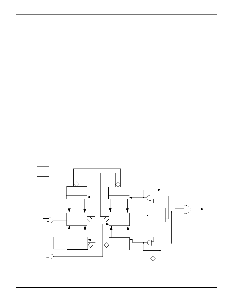
Z8E520/C520
1.5 MBPS USB Device Controller
Zilog
32
P R E L I M I N A R Y
DS97KEY2005
FUNCTIONAL DESCRIPTIONS (Continued)
condition. When the timer control register is written, all tim-
ers that are enabled by the write will begin counting using
the value that is held in their count register. An auto-initial-
ization is not performed. All timers can receive an internal
clock source only, so synchronization of timer updates is
not an issue. Each standard timer that is enabled will be
updated every 8th XTAL clock cycle.
If T0 and T1 are defined to work independently, then each
will work as an 8-bit timer with a single auto-initialization
register; T0ARLO for T0, and T1ARLO for T1. Each timer
will assert its predefined interrupt when it times out, and
will optionally perform the auto-initialization function. If T0
and T1 are cascaded to form a single 16-bit timer, then the
single 16-bit timer will be capable of performing as a Pulse-
Width Modulator (PWM). This timer is referred to as T01 to
distinguish it as having special functionality that is not
available when T0 and T1 act independently.
When T01 is enabled, it can use a pair of 16-bit auto-initial-
ization registers. In this mode, one 16-bit auto-initialization
value is composed of the concatenation of T1ARLO and
T0ARLO, and the second auto-initialization value is com-
posed of the concatenation of T1ARHI and T0ARHI. When
T01 times out, it will alternately initialize its count value us-
ing the Lo auto-init pair followed by the Hi auto-init pair.
This functionality corresponds to a PWM where the T1 in-
terrupt will define the end of the High section of the wave-
form, and the T0 interrupt will mark the end of the Low por-
tion of the PWM waveform.
To use the cascaded timers as a PWM, one must initialize
the T0/T1 count registers to work in conjunction with the
port pin. The user should initialize the T0 and T1 count reg-
isters to the PWM hi auto-init value to obtain the required
PWM behavior. The PWM is arbitrarily defined to use the
Low auto-reload registers first, implying that it had just
timed out after beginning in the High portion of the PWM
waveform. As such, the PWM is defined to assert the T1
interrupt after the first timeout interval.
After the auto-initialization has been completed, decre-
menting occurs for the number of counts defined by the
auto-init_lo registers. When decrementing again reaches
0, the T0 interrupt is asserted; and auto-init using the auto-
init_hi registers occurs. Decrementing occurs for the num-
ber of counts defined by the auto-init_hi registers until
reaching 0, at which time the the T1 interrupt is asserted,
and the cycle begins again. The internal timers can be
used to trigger external events by toggling port output
when generating an interrupt. This functionality can only
be achieved in conjunction with the port unit defining the
appropriate pin as an output signal with the timer output
special function enabled. In this mode, the appropriate port
output will be toggled when the timer count reaches 0, and
will continue toggling each time that the timer times out.
Figure 18. Z8E520 Timers Block Diagram
XTAL
˜
8
T0ARHI
Register Data Bus
T1ARHI
T0
T1
T1ARLO
T0ARLO
PWM
PA1
˜
8
XTAL
= Bidirectional
OUF
OUF
IRQ0
LOAD
LOAD
IRQ1
T
REG C0≠0
REG C0≠1

Z8E520/C520
Zilog
1.5 MBPS USB Device Controller
DS97KEY2005
P R E L I M I N A R Y
33
1
Watch-Dog Timer. The WDT can be programmed at any-
time in the program operation.
Default value (Reset) = 98 ms
The RC oscillator is under firmware control. If the oscillator
is enabled during USB Suspend/Chip Stop Mode, the de-
vice will be periodically woke up by the WDT timeout. If the
application does not require "motion detect," the current
that drives the internal oscillator/WDT can be saved.
WDT Control Registers. Select time-out values for the
WDT are programmable ≠0 to +100%.
Interrupts. The Z8E520 has six different interrupts. These
interrupts are maskable and prioritized (Figure 19 ). The
six sources are divided as follows:
.
When more than one interrupt is pending, priorities are re-
solved by a programmable priority encoder that is con-
trolled by the Interrupt Priority register. All interrupts are
vectored through locations in the program memory. When
an interrupt machine cycle is activated an interrupt request
is granted. All of the subsequent interrupts are thus dis-
abled, saving the Program Counter and status flags, and
branching to the program memory vector location reserved
for that interrupt. This memory location and the next byte
contain the 16-bit address of the interrupt service routine
for that particular interrupt request.
EMI. Lower EMI on the Z8E520 is achieved through circuit
modifications.
The Z8E520 also accepts external clock from XTAL IN pin
(Figure 20).
Power-On-Reset (POR). A timer circuit is triggered by the
system oscillator and is used for the Power-On Reset
(POR) timer function. The POR time allows V
CC
and the os-
cillator circuit to stabilize before instruction execution be-
gins. POR period is defined as:
The POR timer circuit is a one-shot timer triggered by pow-
er fail to Power OK status. The POR time is a nominal 100
ms at 6 MHz. The POR time is bypassed after Stop-Mode
Recovery.
HALT. HALT turns off the internal CPU clock, but not the
oscillator. The counter/timer and external interrupts
IRQ0≠5 remain active. The Z8E520 recovers by interrupts,
either externally or internally.
USB Reset. Detection by the SIE of a reset from the Host
will cause the chip to reset. The reset will be remembered
so that the program can decide the source of the reset.
The USB Reset will act even if the chip is in the STOP
mode.
Priority
IRQ
0
TCO
1
TC1
2
TC2
3
COMM HIGH
4
COMM LOW
5
Port
Figure 19. Interrupt Block Diagram
IRQ
IMR
6
6
IRQ0≠IRQ4
Vector Select
Interrupt
Request
Global
Interrupt
Enable
Figure 20. Oscillator Configuration
POR (ms) = 98 ms
XTAL1 (in)
XTAL2 (out)

Z8E520/C520
1.5 MBPS USB Device Controller
Zilog
34
P R E L I M I N A R Y
DS97KEY2005
FUNCTIONAL DESCRIPTIONS (Continued)
V
BO
Circuit. The Voltage Brown Out circuit will detect
when voltage has dropped below the normal operating
voltage. The chip will maintain full core functionality and
RAM values will be preserved during the range from V
MIN
(V
CC
= 4V) to V
BO
; however, it may not meet worst case
AC and DC limits. At V
BO
, the chip will be placed in reset
and maintained in that state until V
CC
exceeds V
BO
. When
this condition is reached, the chip will resume operation.
V
BO
is set by design to 2.7 V
±
0.2 V.
STOP. This instruction turns off the internal clock and ex-
ternal ceramic resonator oscillation. It reduces the standby
current to less than 60
µ
A. The STOP Mode is terminated
by an interrupt. An interrupt from any of the active (en-
abled) interrupts will remove the chip from the STOP Mode
(Ports 31≠33 including the USB reset.
Note: The timer cannot generate an interrupt in STOP
Mode because the clock is stopped.
The interrupt causes the processor to restart the applica-
tion program at the address or the vector of the interrupt
and continue the program at the end of the interrupt ser-
vice routine. In order to enter STOP (or HALT) Mode, it is
necessary to first flush the instruction pipeline to avoid sus-
pending execution in mid-instruction. As a result, the user
must execute a NOP (Opcode=FFH) immediately before
the appropriate sleep instruction, such as:
FF
NOP
; clear the pipeline
6F
STOP
; enter STOP Mode
or
FF
NOP
; clear the pipeline
7F
HALT
; enter HALT Mode
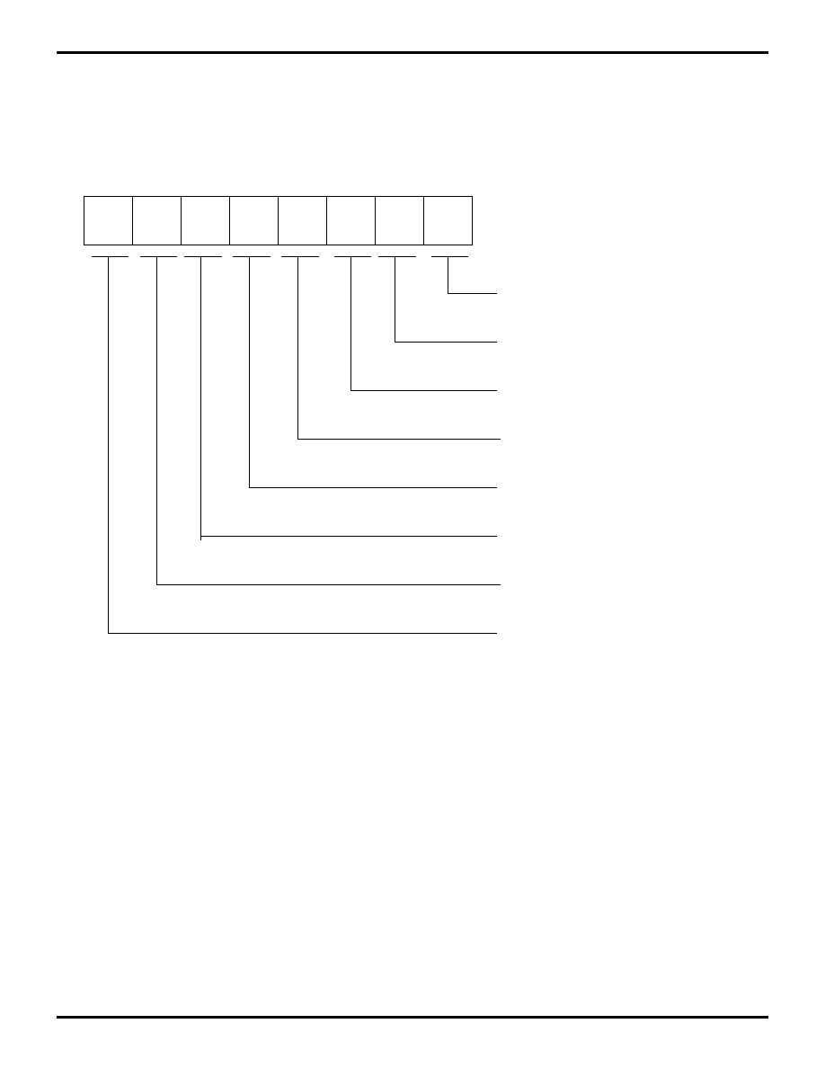
Z8E520/C520
Zilog
1.5 MBPS USB Device Controller
DS97KEY2005
P R E L I M I N A R Y
35
1
Z8
PLUS
SYSTEM REGISTERS
The registers displayed in Figures 21≠27 represent Zilog's
new Z8
Plus
architecture. For a complete overview of this
new technology, please refer to the Z8
Plus
user's manual
(UM97Z8X0300) available at your local Zilog sales office.
Figure 21. Interrupt Request Register
D7
D6
D5
D4
D3
D2
D1
D0
0FA
IRQ
IRQ0 = TIMER0 TIMEOUT
IRQ1 = TIMER1 TIMEOUT
IRQ2 = TIMER2 TIMEOUT
IRQ3 = HIGH PRIORITY COMM
IRQ4 = LOW PRIORITY COMM
IRQ5 = PORTS
RESERVED (MUST BE 0)
RESERVED (MUST BE 0)
FIXED INTERRUPT PRIORITY: IRQ0 > IRQ1 > IRQ2 > IRQ3 > IRQ4 > IRQ5

Z8E520/C520
1.5 MBPS USB Device Controller
Zilog
36
P R E L I M I N A R Y
DS97KEY2005
Z8PLUS SYSTEM REGISTERS (Continued)
Figure 22. Interrupt Mask Register
Figure 23. Stack Pointer
D7
D6
D5
D4
D3
D2
D1
D0
0FB
IMR
RESERVED (MUST BE 0)
1 = IRQ BIT N ENABLED
0 = IRQ BIT N MASKED
1= GLOBAL INTERRUPTS ENABLED
0 = GLOBAL INTERRUPTS DISABLED
D7
D6
D5
D4
D3
D2
D1
D0
0FF
STACK POINTER
NEXT STACK ADDRESSES

Z8E520/C520
Zilog
1.5 MBPS USB Device Controller
DS97KEY2005
P R E L I M I N A R Y
37
1
Figure 24. TCTLHI Register
D7
D6
D5
D4
D3
D2
D1
D0
0C1
TCTLHI
RESET SOURCE
0 = STOP MODE ENABLED
1 = STOP MODE DISABLED
D6 D5 D4 WDT TIMEOUT VALUE
0 0 0 DISABLED
0 0 1 65,536
0 1 0 131,072
0 1 1 262,144
1 0 0 524,288
1 0 1 1,048,576
1 1 0 2,097,152 156 400 1200.0
1 1 1 4,194,304
(RC CLOCKS TO TIMEOUT)
1 = RC ENABLED
0 = RC DISABLED
5 12 39.3 mS
10 25 78.0 mS
19 50 156.0 mS
38 100 312.0 mS
78 200 624.0 mS
COUNTS MIN NOM MAX
300 800 2400.0 mS
UNITS
mS
SIE WDT POR
: RC FREQUENCY = 40 KHz (Range: 20 TO 100 KHz)
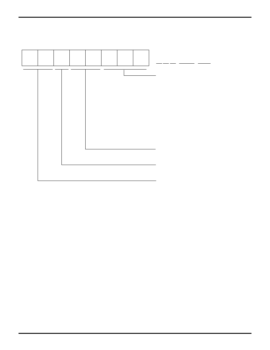
Z8E520/C520
1.5 MBPS USB Device Controller
Zilog
38
P R E L I M I N A R Y
DS97KEY2005
Z8PLUS SYSTEM REGISTERS (Continued)
Figure 25. TCTLLO Register
D7
D6
D5
D4
D3
D2
D1
D0
0C0
TCTLLO
TIMER STATUS
D2 D1 D0 T0 T1
0 0 0 DISAB. DISAB.
0 0 1 ENAB. DISAB.
0 1 0 DISAB. ENAB.
0 1 1 ENAB. ENAB.
1 0 0 T01 (PWM)
1 0 1 ENAB.(*) DISAB.
1 1 0 DISAB. ENAB.(*)
1 1 1 T32 (16 BIT)
(NOTE: (*) INDICATES AUTO-RELOAD
IS ACTIVE.)
1 = T32 16-BIT TIMER ENABLED WITH
AUTO-RELOAD ACTIVE
0 = T2 AND T3 TIMERS DISABLED
D6 1: PWM MODE IN T0 (PA1 IS OUTPUT)
NOTE: TIMER T01 IS A 16-BIT PWM TIMER FORMED BY CASCADING 8-BIT TIMERS
T1 (MSB) AND T0 (LSB). TIMER T32 IS A STANDARD 16-BIT TIMER FORMED
BY CASCADING 8-BIT TIMERS T3(MSB) AND T2(LSB).
D3 0: 6 MHz CR
NOTE: CLOCK "DIVIDE BY" MODE (
˜
) ALLOWS FOR LOWER POWER FOR RS232 OR FASTER
CPU EXECUTION WITH ZIE AT NORMAL 6 MHZ CLOCK RATE.
D3 1: 12 MHz CR
D4 0: CORE CLK =
˜
(XTAL VALUE)
D4 1: CORE CLK = XTAL
˜
2
D7 1: CAPTURE MODE IN T0 (PA0 IS INPUT)
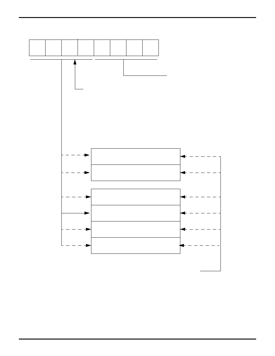
Z8E520/C520
Zilog
1.5 MBPS USB Device Controller
DS97KEY2005
P R E L I M I N A R Y
39
1
Figure 26. Z8E520 Register Pointe
D7
D6
D5
D4
D3
D2
D1
D0
0FD
RP
MUST BE 0. (ONLY PAGE0 IS
IMPLEMENTED ON Z8E520.)
DF
D0
CF
C0
3F
30
2F
20
1F
10
0F
00
The upper nibble of the register file address
provided by the register pointer specifies
the active working register group.
Register Pointer
R15
R0
R15
R0
R15
R0
R15
R0
R15
R0
R15
R0
Register Group 0
Register Group 1
Register Group 2 * (ACTIVE)
Register Group 3
Register Group C
Register Group D
The lower nibble of the register
file address provided by the
instruction points to the
specific register.
* Register Group 2 is active if RP = 20H.
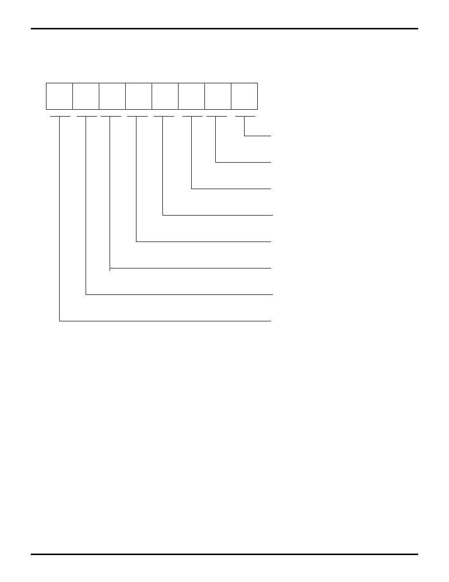
Z8E520/C520
1.5 MBPS USB Device Controller
Zilog
40
P R E L I M I N A R Y
DS97KEY2005
Z8PLUS SYSTEM REGISTERS (Continued)
Figure 27. Flags Register
D7
D6
D5
D4
D3
D2
D1
D0
0FC
FLAGS
STOP MODE RECOVERY FLAG (SMR)
WDT RESET FLAG (WDT)
HALF-CARRY FLAG (HC)
DECIMAL ADJUST FLAG (DA)
OVERFLOW FLAG (OVF)
SIGN FLAG (S)
ZERO FLAG (Z)
CARRY FLAG (C)
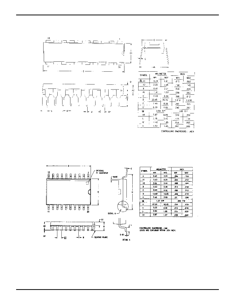
Z8E520/C520
Zilog
1.5 MBPS USB Device Controller
DS97KEY2005
P R E L I M I N A R Y
41
1
PACKAGE INFORMATION
Figure 28. 20-Pin DIP Package
Figure 29. 20-Pin SOIC Package

Z8E520/C520
1.5 MBPS USB Device Controller
Zilog
42
P R E L I M I N A R Y
DS97KEY2005
ORDERING INFORMATION
For fast results, contact your Zilog sales office for assistance in ordering the part required.
CODES
Package
P = Plastic DIP
V = Plastic Leaded Chip Carrier
F = Quad Flat Pack
Speed
06 = 6 MHz
Environment
C = Plastic Standard
Temperature
S = 0
∞
C to +70
∞
C
6 MHz
6 MHz
20-Pin DIP
20-Pin SOIC
Z8E520PSC
Z8E520SSC
Z8C520PSC
Z8C520SSC
Example:
Z 8E520 06 P S C
Environmental Flow
Temperature
Package
Speed
Product Number
Zilog Prefix
is a Z8E520, 6 MHz, SOIC
, 0
∞
C to +70
∞
C, Plastic Standar d Flow

Z8E520/C520
Zilog
1.5 MBPS USB Device Controller
DS97KEY2005
P R E L I M I N A R Y
43
1
Development Projects:
Customer is cautioned that while reasonable efforts will be
employed to meet performance objectives and milestone
dates, development is subject to unanticipated problems
and delays. No production release is authorized or
committed until the Customer and Zilog have agreed upon
a Customer Procurement Specification for this product.
Pre-Characterization Product:
The product represented by this CPS is newly introduced
and Zilog has not completed the full characterization of the
product. The CPS states what Zilog knows about this
product at this time, but additional features or
nonconformance with some aspects of the CPS may be
found, either by Zilog or its customers in the course of
further application and characterization work. In addition,
Zilog cautions that delivery may be uncertain at times, due
to start-up yield issues.
Low Margin:
Customer is advised that this product does not meet
Zilog's internal guardbanded test policies for the
specification requested and is supplied on an exception
basis. Customer is cautioned that delivery may be
uncertain and that, in addition to all other limitations on
Zilog liability stated on the front and back of the
acknowledgment, Zilog makes no claim as to quality and
reliability under the CPS. The product remains subject to
standard warranty for replacement due to defects in
materials and workmanship.
© 1998 by Zilog, Inc. All rights reserved. No part of this
document may be copied or reproduced in any form or by
any means without the prior written consent of Zilog, Inc.
The information in this document is subject to change
without notice. Devices sold by Zilog, Inc. are covered by
warranty and patent indemnification provisions appearing
in Zilog, Inc. Terms and Conditions of Sale only.
ZILOG, INC. MAKES NO WARRANTY, EXPRESS,
STATUTORY, IMPLIED OR BY DESCRIPTION,
REGARDING THE INFORMATION SET FORTH HEREIN
OR REGARDING THE FREEDOM OF THE DESCRIBED
DEVICES FROM INTELLECTUAL PROPERTY
INFRINGEMENT. ZILOG, INC. MAKES NO WARRANTY
OF MERCHANTABILITY OR FITNESS FOR ANY
PURPOSE.
Zilog, Inc. shall not be responsible for any errors that may
appear in this document. Zilog, Inc. makes no commitment
to update or keep current the information contained in this
document.
Zilog's products are not authorized for use as critical
components in life support devices or systems unless a
specific written agreement pertaining to such intended use
is executed between the customer and Zilog prior to use.
Life support devices or systems are those which are
intended for surgical implantation into the body, or which
sustains life whose failure to perform, when properly used
in accordance with instructions for use provided in the
labeling, can be reasonably expected to result in
significant injury to the user.
Zilog, Inc. 210 East Hacienda Ave.
Campbell, CA 95008-6600
Telephone (408) 370-8000
FAX 408 370-8056
Internet: http://www.zilog.com