
DS001101-Z8X0400
1
D
ATA
S
HEET
Z8E001
1
F
EATURE
-R
ICH
Z8P
LUS
O
NE
-T
IME
P
ROGRAMMABLE
(OTP) M
ICROCONTROLLER
FEATURES
Microcontroller Core Features
•
All Instructions Execute in one 1
µ
s Instruction Cycle
with a 10 MHz Crystal
•
1K x 8 On-Chip OTP EPROM Memory
•
64 x 8 General-Purpose Registers (SRAM)
•
Six Vectored Interrupts with Fixed Priority
•
Operating Speed: DC–10 MHz
•
Six Addressing Modes: R, IR, X, D, RA, & IM
Peripheral Features
•
13 Total Input/Output Pins
•
One 8-Bit I/O Port (Port A)
–
I/O Bit Programmable
–
Each Bit Programmable as Push-Pull or Open-
Drain
•
One 5-Bit I/O Port (Port B)
–
I/O Bit Programmable
–
Includes Special Functionality: Stop-Mode Re-
covery Input, Comparator Inputs, Selectable Edge
Interrupts, and Timer Output
•
One Analog Comparator
•
16-Bit Programmable Watch-Dog Timer (WDT)
•
Software Programmable Timers Configurable as:
–
Two 8-Bit Standard Timers and One 16-Bit Stan-
dard Timer, or
–
One 16-Bit Standard Timer and One 16-Bit Pulse
Width Modulator (PWM) Timer
Additional Features
•
On-Chip Oscillator that accepts an XTAL, Ceramic Res-
onator, LC, or External Clock
•
Programmable Options:
–
EPROM Protect
•
Power Reduction Modes:
–
HALT Mode with Peripheral Units Active
–
STOP Mode with all Functionality Shut Down
CMOS/Technology Features
•
Low-Power Consumption
•
3.5V to 5.5V Operating Range @ 0
∞
C to +70
∞
C
4.5V to 5.5V Operating Range @ –40
∞
C to +105
∞
C
•
18-Pin DIP, SOIC, and 20-Pin SSOP Packages.
GENERAL DESCRIPTION
Allowing easy software development, debug, and prototyp-
ing, ZiLOG’s new Z8E001 Microcontroller (MCU) offers
a cost-effective One-Time Programmable (OTP) solution to
its single-chip Z8Plus MCU family.
For applications demanding powerful I/O capabilities, the
Z8E001’s dedicated input and output lines are grouped into
two ports, and are configurable under software control.
Both 8-bit and 16-bit on-chip timers, with a large number
of user-selectable modes, offload the system of administer-
Part
Number
ROM
(KB)
RAM*
(Bytes)
Speed
(MHz)
Z8E001
1
64
10
Note:
* General-Purpose
Z8E001
Z8Plus OTP Microcontroller
ZiLOG
2
P R E L I M I N A R Y
DS001101-Z8X0400
GENERAL DESCRIPTION
(Continued)
ing real-time tasks such as counting/timing and I/O data
communications.
Note:
All signals with an overline, “ ”, are active Low. For
example, B/
W
(WORD is active Low, only);
B
/W
(BYTE is active Low, only).
Power connections follow conventional descriptions be-
low:
Connection
Circuit
Device
Power
V
CC
V
DD
Ground
GND
V
SS
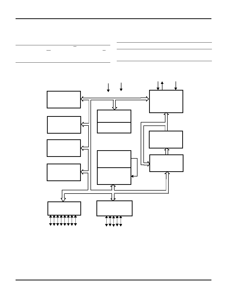
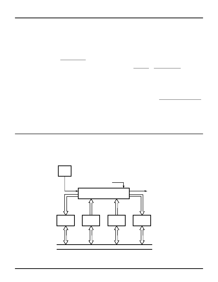
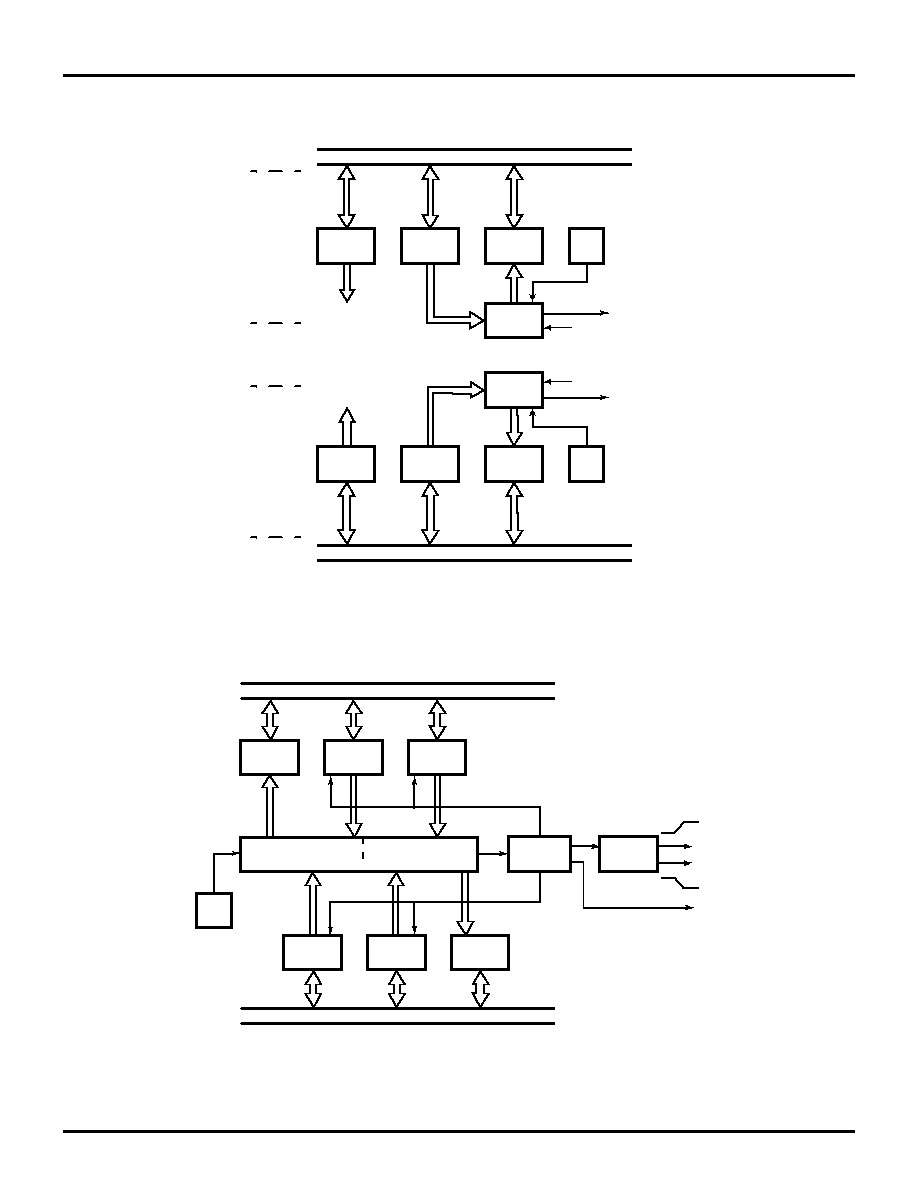
Figure 1. Functional Block Diagram
One 16-bit
Std. Timer
Interrupt
Control
One Analog
Comparator
ALU
FLAG
Register
Pointer
RAM
Register
Machine
Timing
OTP
Prg. Mem-
Program
Counter
V
CC
GND
XTAL
Port A
Port B
I/O
Two 8-bit Timers
or
One 16-bit PWM
Timer
I/O
RESET
Z8E001
ZiLOG
Z8Plus OTP Microcontroller
DS001101-Z8X0400
P R E L I M I N A R Y
3
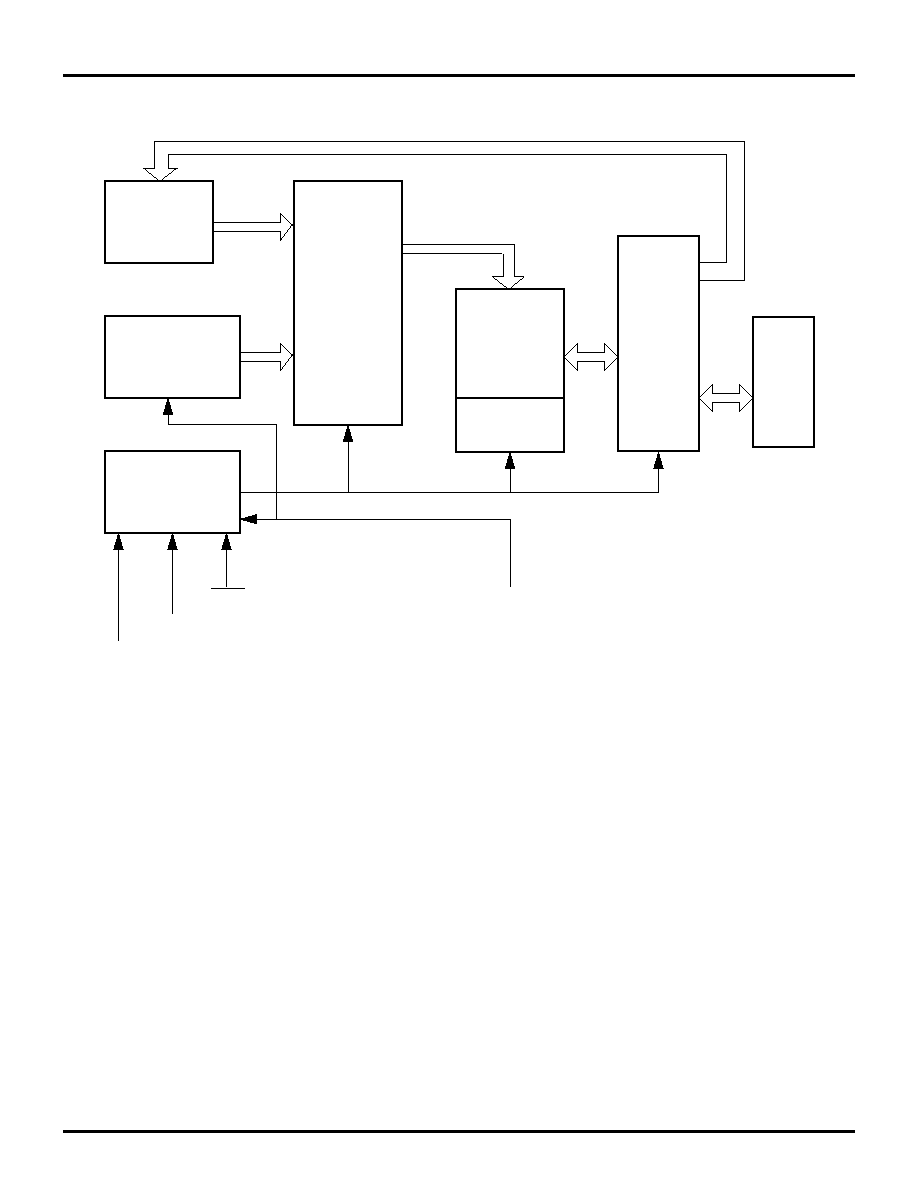
Figure 2. EPROM Programming Mode Block Diagram
Z8E001
PORT
A
DATA
MUX
EPROM
ROM PROT
Z8E001 MCU
ADDRESS
GENERATOR
PGM + TEST
MODE LOGIC
ADDRESS
MUX
D7–0
D7–0
AD9–0
AD9–0
AD9–0
D7–0
ADCLR/V
PP
PGM
ADCLK
XTAL1
OPTION BIT
Z8E001
Z8Plus OTP Microcontroller
ZiLOG
4
P R E L I M I N A R Y
DS001101-Z8X0400
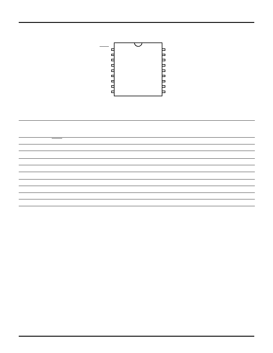
PIN DESCRIPTION
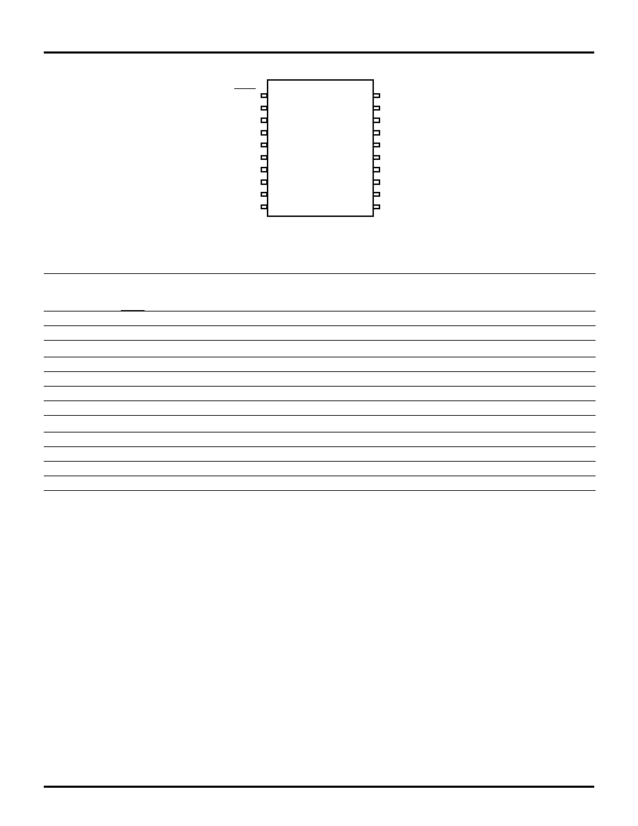
Figure 3. 18-Pin DIP/SOIC Pin Identification/EPROM Programming Mode
EPROM Programming Mode
Pin #
Symbol
Function
Direction
1
PGM
Prog Mode
Input
2–4
GND
Ground
5
ADCLR/V
PP
Clear Clk./Prog Volt.
Input
6-9
D7–D4
Data 7,6,5,4
Input/Output
10–13
D3–D0
Data 3,2,1,0
Input/Output
14
V
DD
Power Supply
15
GND
Ground
16
NC
No Connection
17
XTAL1
1MHz Clock
Input
18
ADCLK
Address Clock
Input
PGM
GND
GND
GND
ADCLR/V
PP
D7
D6
D5
D4
ADCLK
XTAL1
NC
GND
V
DD
D0
D1
D2
D3
18
18-Pin DIP
1
9
10
Z8E001
ZiLOG
Z8Plus OTP Microcontroller
DS001101-Z8X0400
P R E L I M I N A R Y
5
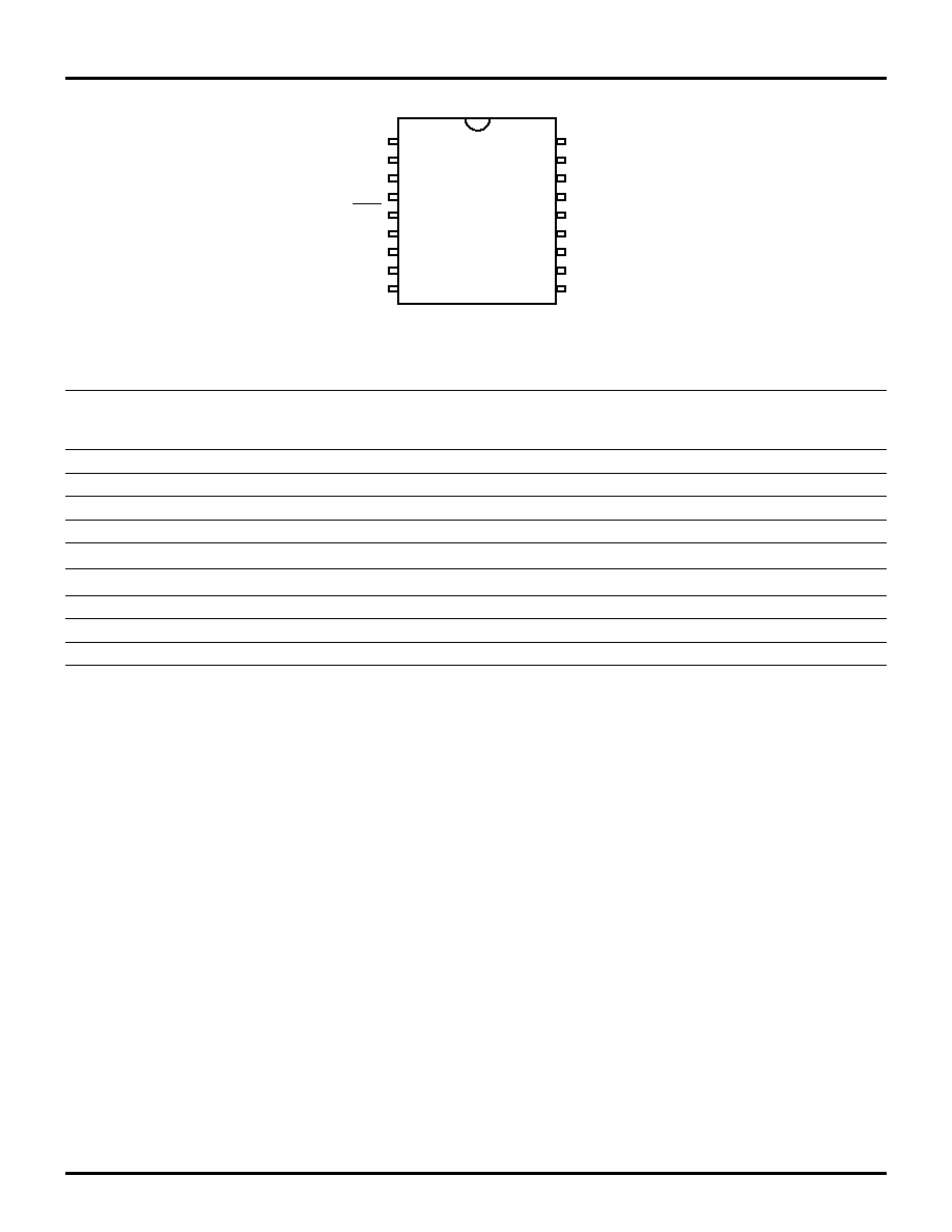
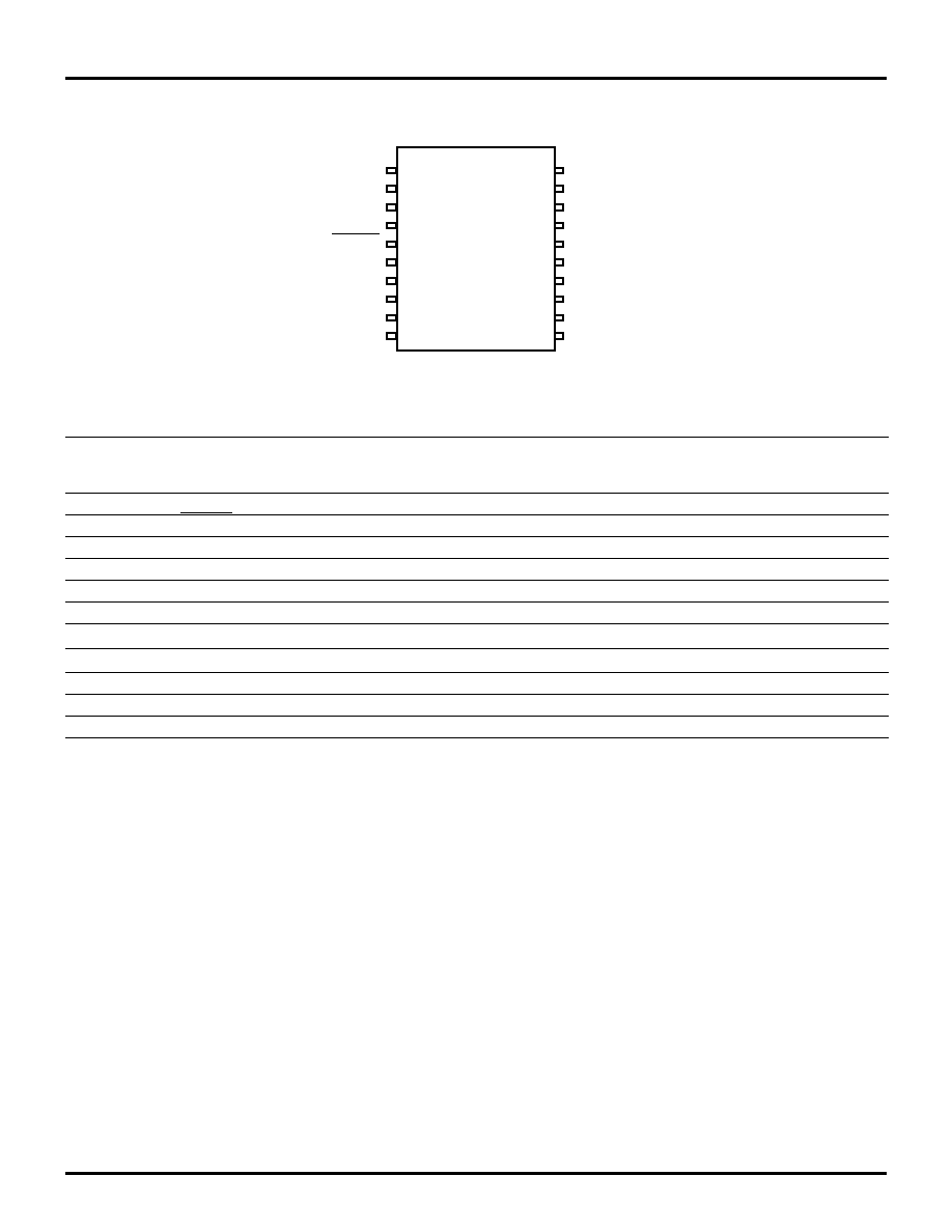
Figure 4. 18-Pin DIP/SOIC Pin Identification
Standard Mode
Pin #
Symbol
Function
Direction
1–4
PB1–PB4
Port B, Pins 1,2,3,4
Input/Output
5
RESET
Reset
Input
6-9
PA7–PA4
Port A, Pins 7,6,5,4
Input/Output
10–13
PA3–PA0
Port A, Pins 3,2,1,0
Input/Output
14
V
CC
Power Supply
15
V
SS
Ground
16
XTAL2
Crystal Osc. Clock
Output
17
XTAL1
Crystal Osc. Clock
Input
18
PB0
Port B, Pin 0
Input/Output
PB1
PB2
PB3
PB4
RST
PA7
PA6
PA5
PA4
PBO
XTAL1
XTAL2
V
SS
V
CC
PA0
PA1
PA2
PA3
18
DIP 18-Pin
1
9
10
Z8E001
Z8Plus OTP Microcontroller
ZiLOG
6
P R E L I M I N A R Y
DS001101-Z8X0400
PIN DESCRIPTION
(Continued)
Figure 5. 20-Pin SSOP Pin Identification
Standard Mode
Pin #
Symbol
Function
Direction
1–4
PB1–PB4
Port B, Pins 1,2,3,4
Input/Output
5
RESET
Reset
Input
6
NC
No Connection
7–10
PA7–PA4
Port A, Pins 7,6,5,4
Input/Output
11–14
PA3–PA0
Port A, Pins 3,2,1,0
Input/Output
15
NC
No Connection
16
V
CC
Power Supply
17
V
SS
Ground
18
XTAL2
Crystal Osc. Clock
Output
19
XTAL1
Crystal Osc. Clock
Input
20
PB0
Port B, Pin 0
Input/Output
PB1
PB2
PB3
PB4
RESET
NC
PA7
PA6
PA5
PA4
PBO
XTAL1
XTAL2
V
SS
V
CC
NC
PA0
PA1
PA2
PA3
20
SSOP 20-Pin
1
10
11
Z8E001
ZiLOG
Z8Plus OTP Microcontroller
DS001101-Z8X0400
P R E L I M I N A R Y
7
Figure 6. 20-Pin SSOP Pin Identification/EPROM Programming Mode
EPROM Programming Mode
Pin #
Symbol
Function
Direction
1
PGM
Prog Mode
Input
2–4
GND
Ground
5
ADCLR/V
PP
Clear Clk./Prog Volt.
Input
6
NC
No Connection
7–10
D7–D4
Data 7,6,5,4
Input/Output
11–14
D3–D0
Data 3,2,1,0
Input/Output
15
NC
No Connection
16
V
DD
Power Supply
17
GND
Ground
18
NC
No Connection
19
XTAL1
1MHz Clock
Input
20
ADCLK
Address Clock
Input
PGM
GND
GND
GND
ADCLR/V
PP
NC
D7
D6
D5
D4
ADCLK
XTAL1
NC
GND
V
DD
NC
D0
D1
D2
D3
20
SSOP 20-Pin
1
10
11

Z8E001
Z8Plus OTP Microcontroller
ZiLOG
8
P R E L I M I N A R Y
DS001101-Z8X0400
ABSOLUTE MAXIMUM RATINGS
Stresses greater than those listed under Absolute Maximum
Ratings can cause permanent damage to the device. This rat-
ing is a stress rating only. Functional operation of the device
at any condition above those indicated in the operational
sections of these specifications is not implied. Exposure to
absolute maximum rating conditions for an extended period
can affect device reliability. Total power dissipation should
not exceed 880 mW for the package. Power dissipation is
calculated as follows:
Parameter
Min
Max
Units
Note
Ambient Temperature under Bias
–40
+105
C
Storage Temperature
–65
+150
C
Voltage on any Pin with Respect to V
SS
–0.6
+7
V
1
Voltage on V
DD
Pin with Respect to V
SS
–0.3
+7
V
Voltage on RESET Pin with Respect to V
SS
–0.6
V
DD
+1
V
2
Total Power Dissipation
880
mW
Maximum Allowable Current out of V
SS
80
mA
Maximum Allowable Current into V
DD
80
mA
Maximum Allowable Current into an Input Pin
–600
+600
mA
3
Maximum Allowable Current into an Open-Drain Pin
–600
+600
mA
4
Maximum Allowable Output Current Sunk by Any I/O Pin
25
mA
Maximum Allowable Output Current Sourced by Any I/O Pin
25
mA
Maximum Allowable Output Current Sunk by Port A
40
mA
Maximum Allowable Output Current Sourced by Port A
40
mA
Maximum Allowable Output Current Sunk by Port B
40
mA
Maximum Allowable Output Current Sourced by Port B
40
mA
Notes:
1. Applies to all pins except the RESET pin and where otherwise noted.
2. There is no input protection diode from pin to V
DD
.
3. Excludes XTAL pins.
4. Device pin is not at an output Low state.
Total Power Dissipation = V
DD
x [I
DD
– (sum of I
OH
)]
+ sum of [(V
DD
– V
OH
) x I
OH
]
+ sum of (V
0L
x I
0L
)
Z8E001
ZiLOG
Z8Plus OTP Microcontroller
DS001101-Z8X0400
P R E L I M I N A R Y
9
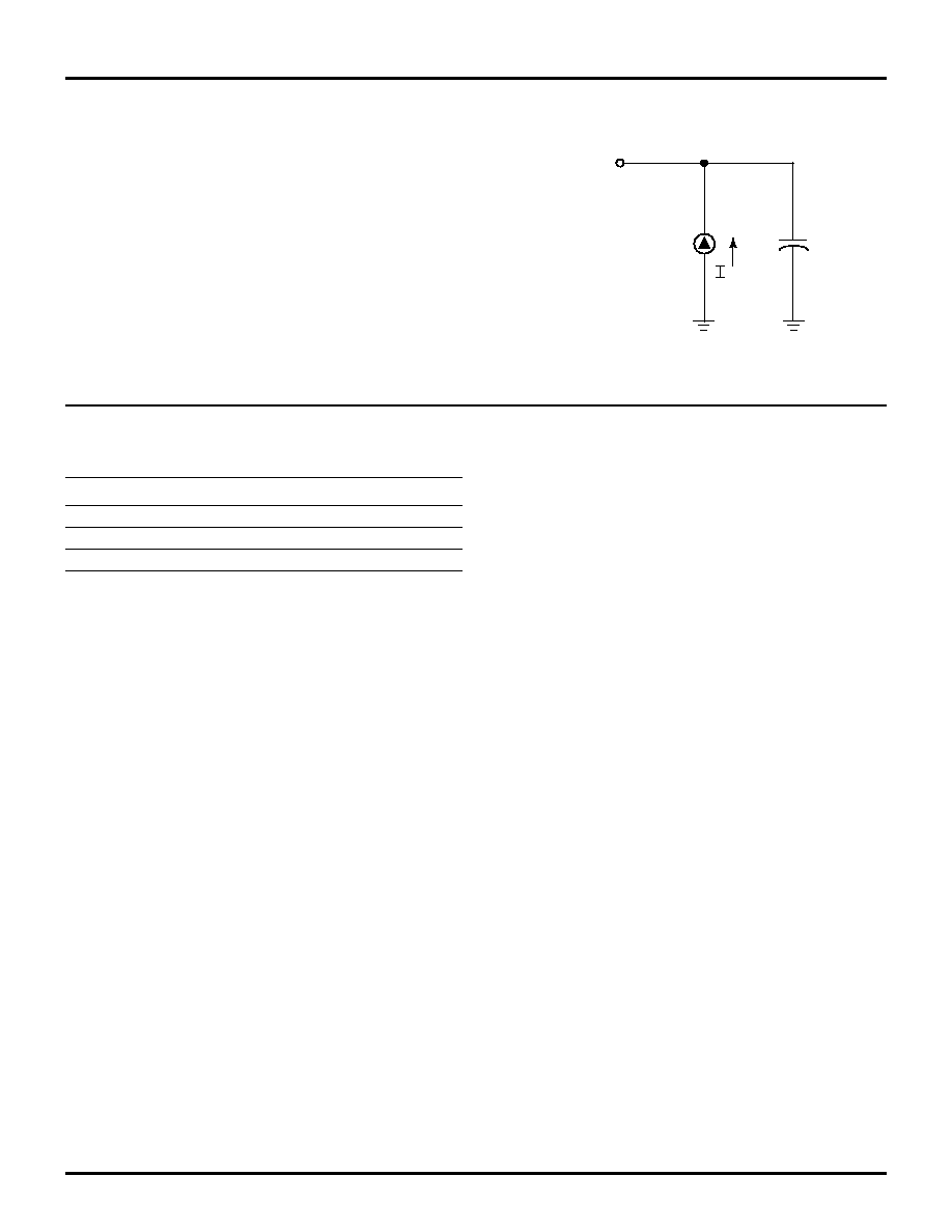
STANDARD TEST CONDITIONS
The characteristics listed below apply for standard test con-
ditions as noted. All voltages are referenced to Ground. Pos-
itive current flows into the referenced pin (Figure 7).
CAPACITANCE
T
A
= 25°C, V
CC
= GND = 0V, f = 1.0 MHz, unmeasured pins returned to GND.
Figure 7. Test Load Diagram
From Output
Under Test
150 pF
Parameter
Min
Max
Input capacitance
0
12 pF
Output capacitance
0
12 pF
I/O capacitance
0
12 pF

Z8E001
Z8Plus OTP Microcontroller
ZiLOG
10
P R E L I M I N A R Y
DS001101-Z8X0400
DC ELECTRICAL CHARACTERISTICS
Table 1. DC Electrical Characteristics
pF T
A
= 0°C to +70°C
Standard Temperatures
Typical
2
@ 25°C
Sym
Parameter
V
CC
1
Min
Max
Units Conditions
Notes
V
CH
Clock Input High
Voltage
3.5V
0.7V
CC
V
CC
+0.3
1.3
V
Driven by External
Clock Generator
5.5V
0.7V
CC
V
CC
+0.3
2.5
V
Driven by External
Clock Generator
V
CL
Clock Input Low
Voltage
3.5V
V
SS
–0.3
0.2V
CC
0.7
V
Driven by External
Clock Generator
5.5V
V
SS
–0.3
0.2V
CC
1.5
V
Driven by External
Clock Generator
V
IH
Input High Voltage
3.5V
5.5V
0.7V
CC
0.7V
CC
V
CC
+0.3
V
CC
+0.3
1.3
2.5
V
V
V
IL
Input Low Voltage
3.5V
5.5V
V
SS
–0.3
V
SS
–0.3
0.2V
CC
0.2V
CC
0.7
1.5
V
V
V
OH
Output High Voltage
3.5V
V
CC
–0.4
3.1
V
I
OH
= –2.0 mA
5.5V
V
CC
–0.4
4.8
V
I
OH
= –2.0 mA
V
OL1
Output Low Voltage
3.5V
0.6
0.2
V
I
OL
= +4.0 mA
5.5V
0.4
0.1
V
I
OL
= +4.0 mA
V
OL2
Output Low Voltage
3.5V
1.2
0.5
V
I
OL
= +6 mA
5.5V
1.2
0.5
V
I
OL
= +12 mA
V
RH
Reset Input High
Voltage
3.5V
0.5V
CC
V
CC
1.1
V
5.5V
0.5V
CC
V
CC
2.2
V
V
RL
Reset Input Low
Voltage
3.5V
V
SS
–0.3
0.2V
CC
0.9
V
5.5V
V
SS
–0.3
0.2V
CC
1.4
V
V
OFFSET
Comparator Input
Offset Voltage
3.5V
25.0
10.0
mV
5.5V
25.0
10.0
mV
I
IL
Input Leakage
3.5V
–1.0
2.0
0.064
mA
V
IN
= 0V, V
CC
5.5V
–1.0
2.0
0.064
mA
V
IN
= 0V, V
CC
I
OL
Output Leakage
3.5V
–1.0
2.0
0.114
µA
V
IN
= 0V, V
CC
5.5V
–1.0
2.0
0.114
µA
V
IN
= 0V, V
CC
V
ICR
Comparator Input
Common Mode
Voltage Range
3.5V
V
SS
–0.3
V
CC
–1.0
V
3
5.5V
V
SS
–0.3
V
CC
–1.0
V
3
I
IR
Reset Input Current
3.5V
–10
–60
–30
µA
5.5V
–20
–180
–100
µA

Z8E001
ZiLOG
Z8Plus OTP Microcontroller
DS001101-Z8X0400
P R E L I M I N A R Y
11
I
CC
Supply Current
3.5V
2.5
2.0
mA
@ 10 MHz
4,5
5.5V
6.0
3.5
mA
@ 10 MHz
4,5
I
CC1
Standby Current
3.5V
2.0
1.0
mA
HALT Mode V
IN
= 0V,
V
CC
@ 10 MHz
4,5
5.5V
4.0
2.5
mA
HALT Mode V
IN
= 0V,
V
CC
@ 10 MHz
4,5
I
CC2
Standby Current
3.5V
500
150
nA
STOP Mode V
IN
= 0V,
V
CC
6
Notes:
1. The V
CC
voltage specification of 3.5V guarantees 3.5V and the V
CC
voltage specification of 5.5 V guarantees 5.0 V ±0.5 V.
2. Typical values are measured at V
CC
= 3.3V and V
CC
= 5.0V; V
SS
= 0V = GND.
3. For analog comparator input when analog comparator is enabled.
4. All outputs unloaded and all inputs are at V
CC
or V
SS
level.
5. CL1 = CL2 = 22 pF.
6. Same as note 4 except inputs at V
CC
.
Table 1. DC Electrical Characteristics (Continued)
pF T
A
= 0°C to +70°C
Standard Temperatures
Typical
2
@ 25°C
Sym
Parameter
V
CC
1
Min
Max
Units Conditions
Notes

Z8E001
Z8Plus OTP Microcontroller
ZiLOG
12
P R E L I M I N A R Y
DS001101-Z8X0400
DC ELECTRICAL CHARACTERISTICS (Continued)
Table 2. DC Electrical Characteristics
T
A
= –40°C to +105°C
Extended Temperatures
Typical
2
@ 25°C
Sym
Parameter
V
CC
1
Min
Max
Units Conditions
Notes
V
CH
Clock Input High
Voltage
4.5V
0.7 V
CC
V
CC
+0.3
2.5
V
Driven by External
Clock Generator
5.5V
0.7 V
CC
V
CC
+0.3
2.5
V
Driven by External
Clock Generator
V
CL
Clock Input Low
Voltage
4.5V
V
SS
–0.3
0.2 V
CC
1.5
V
Driven by External
Clock Generator
5.5V
V
SS
–0.3
0.2 V
CC
1.5
V
Driven by External
Clock Generator
V
IH
Input High Voltage
4.5V
0.7 V
CC
V
CC
+0.3
2.5
V
5.5V
0.7 V
CC
V
CC
+0.3
2.5
V
V
IL
Input Low Voltage
4.5V
V
SS
–0.3
0.2 V
CC
1.5
V
5.5V
V
SS
–0.3
0.2 V
CC
1.5
V
V
OH
Output High Voltage
4.5V
V
CC
–0.4
4.8
V
I
OH
= –2.0 mA
5.5V
V
CC
–0.4
4.8
V
I
OH
= –2.0 mA
V
OL1
Output Low Voltage
4.5V
0.4
0.1
V
I
OL
= +4.0 mA
5.5V
0.4
0.1
V
I
OL
= +4.0 mA
V
OL2
Output Low Voltage
4.5V
1.2
0.5
V
I
OL
= +12 mA
5.5V
1.2
0.5
V
I
OL
= +12 mA
V
RH
Reset Input High
Voltage
4.5V
0.5V
CC
V
CC
1.1
V
5.5V
0.5V
CC
V
CC
2.2
V
V
OFFSET
Comparator Input
Offset Voltage
4.5V
25.0
10.0
mV
5.5V
25.0
10.0
mV
I
IL
Input Leakage
4.5V
–1.0
2.0
<1.0
µA
V
IN
= 0V, V
CC
5.5V
–1.0
2.0
<1.0
µA
V
IN
= 0V, V
CC
I
OL
Output Leakage
4.5V
–1.0
2.0
<1.0
µA
V
IN
= 0V, V
CC
5.5V
–1.0
2.0
<1.0
µA
V
IN
= 0V, V
CC
V
ICR
Comparator Input
Common Mode
Voltage Range
4.5V
0 V
CC
–1.5V
V
3
5.5V
0
V
CC
–1.5V
V
3
I
IR
Reset Input Current
4.5V
–18
–180
–112
mA
5.5V
–18
–180
–112
mA

Z8E001
ZiLOG
Z8Plus OTP Microcontroller
DS001101-Z8X0400
P R E L I M I N A R Y
13
I
CC
Supply Current
4.5V
7.0
4.0
mA
@ 10 MHz
4,5
5.5V
7.0
4.0
mA
@ 10 MHz
4,5
I
CC1
Standby Current
4.5V
2.0
1.0
mA
HALT Mode V
IN
= 0V,
V
CC
@ 10 MHz
4,5
5.5V
2.0
1.0
mA
HALT Mode V
IN
= 0V,
V
CC
@ 10 MHz
4,5
I
CC2
Standby Current
4.5V
700
250
nA
STOP Mode V
IN
= 0V,V
CC
6
5.5V
700
250
nA
STOP Mode V
IN
= 0V,V
CC
6
Notes:
1. The V
CC
voltage specification of 4.5V and 5.5V guarantees 5.0V ±0.5V.
2. Typical values are measured at V
CC
= 3.3V and V
CC
= 5.0V; V
SS
= 0V = GND.
3. For analog comparator input when analog comparator is enabled.
4. All outputs unloaded and all inputs are at V
CC
or V
SS
level.
5. CL1 = CL2 = 22 pF.
6. Same as note 4 except inputs at V
CC
.
Table 2. DC Electrical Characteristics (Continued)
T
A
= –40°C to +105°C
Extended Temperatures
Typical
2
@ 25°C
Sym
Parameter
V
CC
1
Min
Max
Units Conditions
Notes
Z8E001
Z8Plus OTP Microcontroller
ZiLOG
14
P R E L I M I N A R Y
DS001101-Z8X0400
AC ELECTRICAL CHARACTERISTICS
Figure 8. AC Electrical Timing Diagram
Table 3. Additional Timing
T
A
= 0°C to +70°C
T
A
= –40°C to +105°C
@ 10 MHz
No
Symbol
Parameter
V
CC
1
Min
Max
Units
Notes
1
TpC
Input Clock Period
3.5V
100
DC
ns
2
5.5V
100
DC
ns
2
2
TrC,TfC
Clock Input Rise and Fall Times
3.5V
15
ns
2
5.5V
15
ns
2
3
TwC
Input Clock Width
3.5V
50
ns
2
5.5V
50
ns
2
4
TwIL
Int. Request Input Low Time
3.5V
70
ns
2
5.5V
70
ns
2
5
TwIH
Int. Request Input High Time
3.5V
5TpC
2
5.5V
5TpC
2
6
Twsm
STOP Mode Recovery Width
Spec.
3.5V
12
ns
5.5V
12
ns
7
Tost
Oscillator Start-Up Time
3.5V
5TpC
5.5V
5TpC
Notes:
1. The V
DD
voltage specification of 3.5V guarantees 3.5V. The V
DD
voltage specification of 5.5V guarantees 5.0V
±
0.5V.
2. Timing Reference uses 0.7 V
CC
for a logic 1 and 0.2 V
CC
for a logic 0.
1
3
3
2
2
CLOCK
IRQ
N
4
5

Z8E001
ZiLOG
Z8Plus OTP Microcontroller
DS001101-Z8X0400
P R E L I M I N A R Y
15
Z8PLUS CORE
The Z8E001 is based on the ZiLOG Z8Plus Core Architec-
ture. This core is capable of addressing up to 64KBytes of
program memory and 4KBytes of RAM. Register RAM is
accessed as either 8 or 16 bit registers using a combination
of 4, 8, and 12 bit addressing modes. The architecture sup-
ports up to 15 vectored interrupts from external and internal
sources. The processor decodes 44 CISC instructions using
six addressing modes. See the Z8Plus User’s Manual for
more information.
RESET
This section describes the Z8E001 reset conditions, reset
timing, and register initialization procedures. Reset is gen-
erated by the Reset Pin, Watch-Dog Timer (WDT), and
Stop-Mode Recovery (SMR).
A system reset overrides all other operating conditions and
puts the Z8E001 into a known state. To initialize the chip’s
internal logic, the RESET input must be held Low for at
least 30 XTAL clock cycles. The control registers and ports
are reset to their default conditions after a reset from
the RESET pin. The control registers and ports are not reset
to their default conditions after wakeup from Stop Mode or
WDT timeout.
During RESET, the program counter is loaded with 0020H.
I/O ports and control registers are configured to their default
reset state. Resetting the Z8E001 does not affect the con-
tents of the general-purpose registers.
RESET PIN OPERATION
The Z8E001 hardware RESET pin initializes the control
and peripheral registers, as shown in Table 4. Specific reset
values are shown by 1 or 0, while bits whose states are un-
changed or unknown from Power-Up are indicated by the
letter U.
RESET must be held Low until the oscillator stabilizes, for
an additional 30 XTAL clock cycles, in order to be sure that
the internal reset is complete. The RESET pin has a Schmitt-
Trigger input with a trip point. There is no High side pro-
tection diode. The user should place an external diode from
RESET to V
CC
. A pull-up resistor on the RESET pin is ap-
proximately 500 K
, typical.
Program execution starts 10 XTAL clock cycles after RE-
SET has returned High. The initial instruction fetch is from
location 0020H. Figure 9 indicates reset timing.
After a reset, the first routine executed must be one that ini-
tializes the TCTLHI control register to the required system
configuration, followed by initialization of the remaining
control registers.
Table 4. Control and Peripheral Registers
Register (HEX)
Register Name
Bits
Comments
7
6
5
4
3
2
1
0
FF
Stack Pointer
0
0
U
U
U
U
U
U
Stack pointer is not affected by
RESET
FE
Reserved
FD
Register Pointer
U
U
U
U
0
0
0
0
Register pointer is not affected by
RESET
FC
Flags
U
U
U
U
U
U
*
*
Only WDT & SMR flags are affected
by RESET
FB
Interrupt Mask
0
0
0
0
0
0
0
0
All interrupts masked by RESET
FA
Interrupt Request
0
0
0
0
0
0
0
0
All interrupt requests cleared by
RESET
F9–F0
Reserved
EF–E0
Virtual Copy
Virtual Copy of the Current Working
Register Set
DF–D8
Reserved

Z8E001
Z8Plus OTP Microcontroller
ZiLOG
16
P R E L I M I N A R Y
DS001101-Z8X0400
RESET PIN OPERATION (Continued)
D7
Port B Special
Function
0
0
0
0
0
0
0
0
Deactivates all port special functions
after RESET
D6
Port B Directional
Control
0
0
0
0
0
0
0
0
Defines all bits as inputs in PortB
after RESET
D5
Port B Output
U
U
U
U
U
U
U
U
Output register not affected by
RESET
D4
Port B Input
U
U
U
U
U
U
U
U
Current sample of the input pin
following RESET
D3
Port A Special
Function
0
0
0
0
0
0
0
0
Deactivates all port special functions
after RESET
D2
Port A Directional
Control
0
0
0
0
0
0
0
0
Defines all bits as inputs in PortA
after RESET
D1
Port A Output
U
U
U
U
U
U
U
U
Output register not affected by
RESET
D0
Port A Input
U
U
U
U
U
U
U
U
Current sample of the input pin
following RESET
CF
Reserved
CE
Reserved
CD
T1VAL
U
U
U
U
U
U
U
U
CC
T0VAL
U
U
U
U
U
U
U
U
CB
T3VAL
U
U
U
U
U
U
U
U
CA
T2VAL
U
U
U
U
U
U
U
U
C9
T3AR
U
U
U
U
U
U
U
U
C8
T2AR
U
U
U
U
U
U
U
U
C7
T1ARHI
U
U
U
U
U
U
U
U
C6
T0ARHI
U
U
U
U
U
U
U
U
C5
T1ARLO
U
U
U
U
U
U
U
U
C4
T0ARLO
U
U
U
U
U
U
U
U
C3
WDTHI
1
1
1
1
1
1
1
1
C2
WDTLO
1
1
1
1
1
1
1
1
C1
TCTLHI
1
1
1
1
1
0
0
0
WDT Enabled in HALT Mode, WDT
timeout at maximum value, STOP
Mode disabled
C0
TCTLLO
0
0
0
0
0
0
0
0
All standard timers are disabled
Note:
*The SMR and WDT flags are set indicating the source of the RESET.
Table 4. Control and Peripheral Registers (Continued)
Register (HEX)
Register Name
Bits
Comments
7
6
5
4
3
2
1
0
Z8E001
ZiLOG
Z8Plus OTP Microcontroller
DS001101-Z8X0400
P R E L I M I N A R Y
17
Table 5. Flag Register Bit D1, D0
D1
D0
Reset Source
0
0
RESET Pin
0
1
SMR Recovery
1
0
WDT Reset
1
1
Reserved
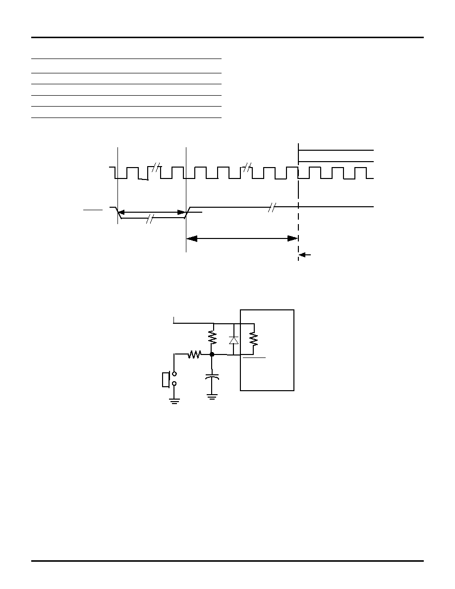
Figure 9. Reset Timing
Figure 10. Example of External Power-On Reset (POR) Circuit
First Machine Cycle
Clock
RESET
First Instruction Fetch
Hold Low For 30 XTAL
Periods (Minimum)
10 XTAL CLOCK CYCLES
1 µF
100 KΩ
RESET
1KΩ
V
CC
Z8E001
V
CC
500 KΩ
Z8E001
Z8Plus OTP Microcontroller
ZiLOG
18
P R E L I M I N A R Y
DS001101-Z8X0400
RESET PIN OPERATION (Continued)
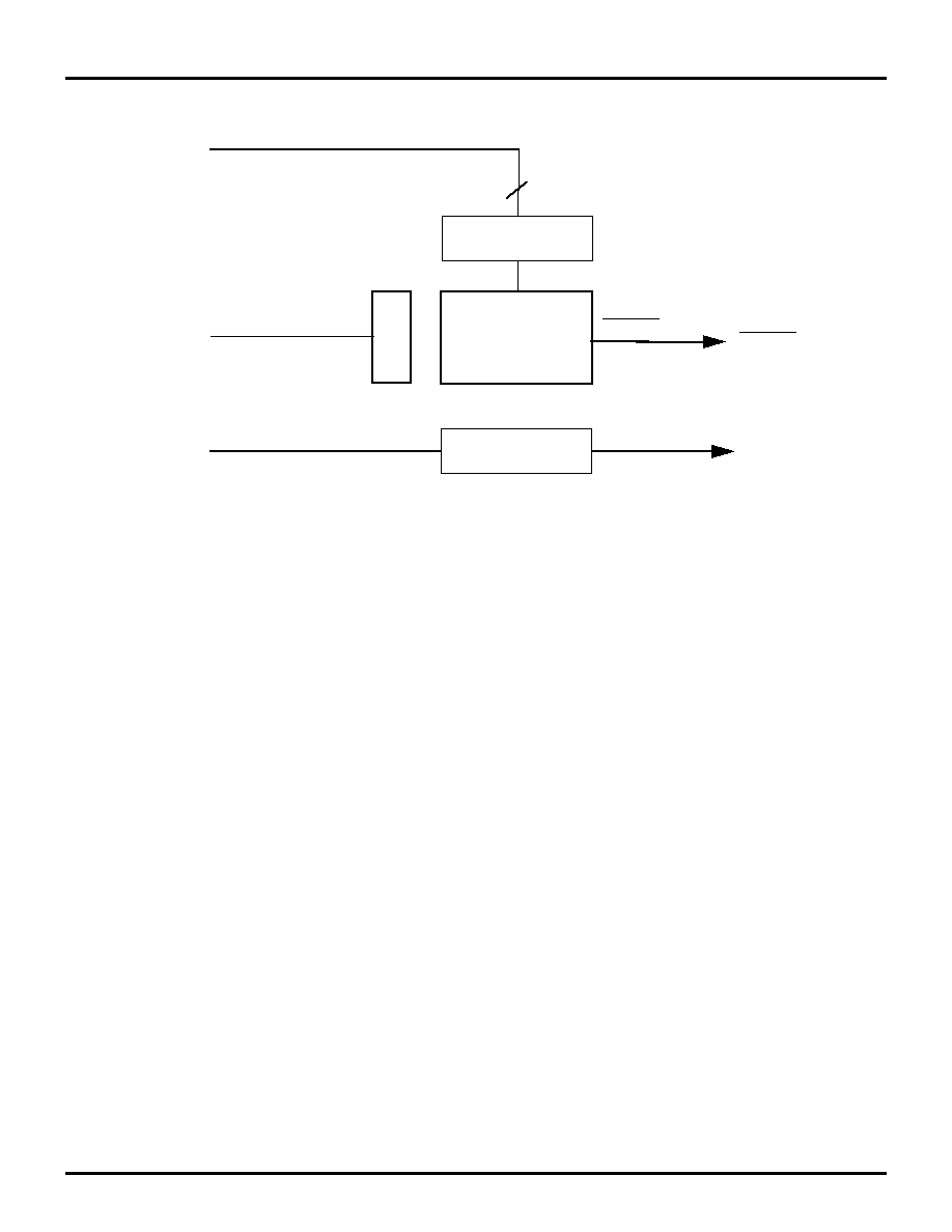
Figure 11. Z8E001 Reset Circuitry with WDT and SMR
XTAL
/64
TCTLHI
D6,D5,D4
3
SMR
RECOVERY
SMR
(PB0)
WDTRST
16-BIT TIMER
WDT TAP SELECT
WDTRST
WATCHDOG TIMER
SMR LOGIC
Z8E001
ZiLOG
Z8Plus OTP Microcontroller
DS001101-Z8X0400
P R E L I M I N A R Y
19
Z8E001 WATCH-DOG TIMER (WDT)
The WDT is a retriggerable one-shot 16-bit timer that resets
the Z8E001
if it reaches its terminal count. The WDT is driv-
en by the XTAL2 clock pin. To provide the longer timeout
periods required in applications, the watchdog timer is only
updated every 64th clock cycle. When operating in the RUN
or HALT Modes, a WDT timeout reset is functionally
equivalent to an interrupt vectoring the PC to 0020H and
setting the WDT flag to a one state. Coming out of RESET,
the WDT is fully enabled with its timeout value set at the
maximum value, unless otherwise programmed during the
first instruction. Subsequent executions of the WDT in-
struction, reinitialize the watchdog timer registers (C2H and
C3H), to their initial values as defined by bits D6, D5, and
D4 of the TCTLHI register. The WDT cannot be disabled
except on the first cycle after RESET, and if the device en-
ters Stop mode.
The WDT instruction should be executed often enough to
provide some margin before allowing the WDT registers to
get near 0. Because the WDT timeout periods are relatively
long, a WDT reset will occur in the unlikely event that the
WDT times out on exactly the same cycle that the WDT in-
struction is executed.
The WDT and SMR flags are the only flags that are affected
by the external RESET pin. RESET clears both the WDT
and SMR flags. A WDT timeout sets the WDT flag. The
STOP instruction sets the SMR flag. This behavior enables
software to determine whether a pin RESET occurred, or
whether a WDT timeout occurred, or whether a return from
STOP Mode occurred. Reading the WDT and SMR flags
does not reset it to zero, the user must clear it via software.
Note: Failure to clear the SMR flag can result in undefined be-
havior.
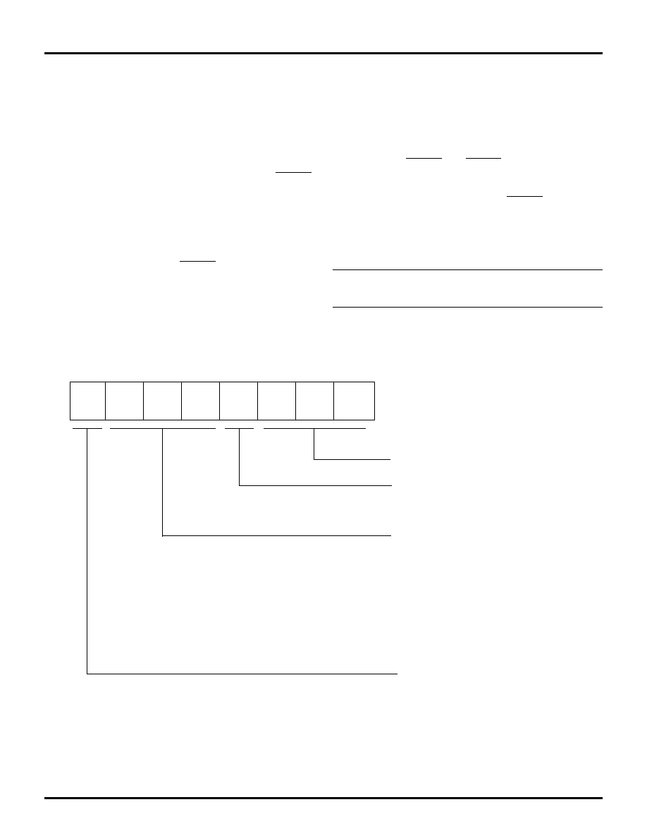
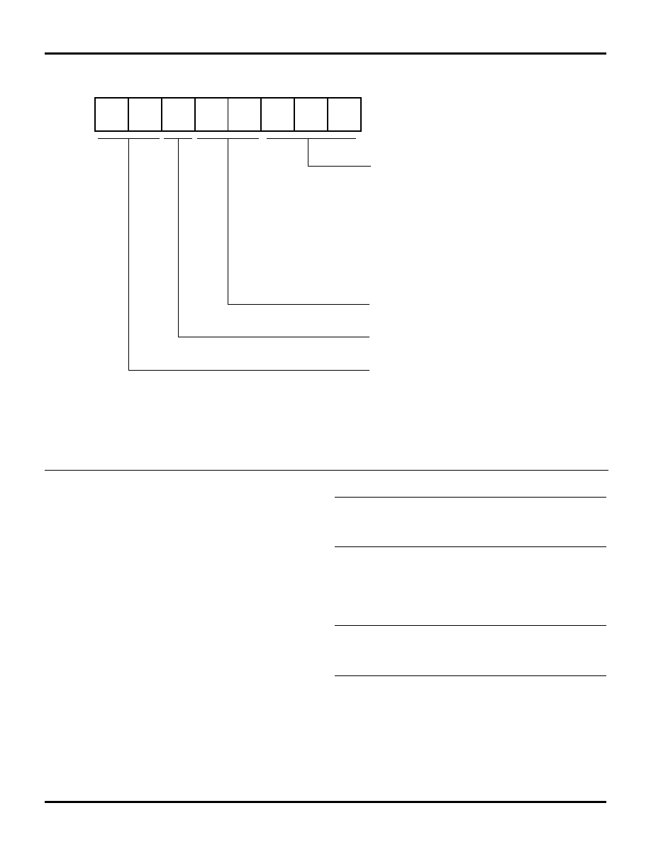
Figure 12. Z8E001 TCTLHI Register for Control of WDT
D7
D6
D5
D4
D3
D2
D1
D0
0C1
TCTLHI
RESERVED (MUST BE 0)
0 = STOP MODE ENABLED
1 = STOP MODE DISABLED*
D6 D5 D4 WDT TIMEOUT VALUE
---- ---- ---- --------------------------------
0 0 0 DISABLED
0 0 1 65,536 TpC
0 1 0 131,072 TpC
0 1 1 262,144 TpC
1 0 0 524,288 TpC
1 0 1 1,048,576 TpC
1 1 0 2,097,152 TpC
1 1 1 4,194,304 TpC*
(XTAL CLOCKS TO TIMEOUT)
1 = WDT ENABLED IN HALT MODE*
0 = WDT DISABLED IN HALT MODE
*Designates Default Value after RESET

Z8E001
Z8Plus OTP Microcontroller
ZiLOG
20
P R E L I M I N A R Y
DS001101-Z8X0400
Note:
The WDT can only be disabled via software if the first
instruction out of RESET performs this function. Logic
within the Z8E001 detects that it is in the process of ex-
ecuting the first instruction after the part leaves RESET.
During the execution of this instruction, the upper five
bits of the TCTLHI register can be written. After this
first instruction, hardware does not allow the upper five
bits of this register to be written.
The TCTLHI bits for control of the WDT are described be-
low:
WDT Time Select (D6, D5, D4).
Bits 6, 5, and 4 determine
the time-out period. Table 6 indicates the range of timeout
values that can be obtained. The default values of D6, D5,
and D4 are all 1, thus setting the WDT to its maximum tim-
eout period when coming out of RESET.
WDT During HALT (D7).
This bit determines whether or
not the WDT is active during HALT Mode. A 1 indicates
active during HALT. A 0 prevents the WDT from resetting
the part while halted.Coming out of reset, the WDT is en-
abled during HALT Mode.
STOP MODE (D3).
Coming out of RESET, the Z8E001
STOP Mode is disabled. If an application requires use of
STOP Mode, bit D3 must be cleared immediately upon
leaving RESET. If bit D3 is set, the STOP instruction exe-
cutes as a NOP. If bit D3 is cleared, the STOP instruction
enters Stop Mode. Whenever the Z8E001 wakes up after
having been in STOP Mode, the STOP Mode is again dis-
abled.
Bits 2, 1 and 0.
These bits are reserved and must be 0.
POWER-DOWN MODES
I
n addition to the standard RUN mode, the Z8
E001
MCU sup-
ports two Power-Down modes to minimize device current con-
sumption. The two modes supported are
HALT and STOP.
HALT MODE OPERATION
The HALT Mode suspends instruction execution and turns
off the internal CPU clock. The on-chip oscillator circuit
remains active so the internal clock continues to run and is
applied to the timers and interrupt logic.
To enter the HALT Mode, the Z8E001 only requires a
HALT instruction. It is NOT necessary to execute a NOP
instruction immediately before the HALT instruction.
The HALT Mode can be exited by servicing an interrupt
(either externally or internally) generated. Upon comple-
tion of the interrupt service routine, the user program con-
tinues from the instruction after the HALT instruction.
The HALT Mode can also be exited via a RESET activation
or a Watch-Dog Timer (WDT) timeout. In these cases, pro-
gram execution restarts at the reset restart address 0020H.
Table 6. WDT Time-Out
D6
D5
D4
Crystal Clocks*
to Timeout
Time-Out Using
a 10 MHZ Crystal
0
0
0
Disabled Disabled
0
0
1
65,536 TpC
6.55 ms
0
1
0
131,072 TpC
13.11 ms
0
1
1
262,144 TpC
26.21 ms
1
0
0
524,288 TpC
52.43 ms
1
0
1
1,048,576 TpC
104.86 ms
1
1
0
2,097,152 TpC
209.72 ms
1
1
1
4,194,304 TpC
419.43 ms
Note:
*
TpC=XTAL clock cycle. The default on reset is D6=D5=D4=1.
7F
HALT
; enter HALT Mode
Z8E001
ZiLOG
Z8Plus OTP Microcontroller
DS001101-Z8X0400
P R E L I M I N A R Y
21
STOP MODE OPERATION
The STOP Mode provides the lowest possible device stand-
by current. This instruction turns off the on-chip oscillator
and internal system clock.
To enter the STOP Mode, the Z8E001 only requires a STOP
instruction. It is NOT necessary to execute a NOP instruc-
tion immediately before the STOP instruction.
The STOP Mode is exited by any one of the following re-
sets: RESET pin or a STOP-Mode Recovery source. Upon
reset generation, the processor always restarts the applica-
tion program at address 0020H, and the STOP Mode Flag
is set. Reading the STOP Mode Flag does not clear it. The
user must clear the STOP Mode Flag with software.
Note:
Failure to clear the STOP Mode Flag can result in unde-
fined behavior.
The Z8E001 provides a dedicated STOP-Mode Recovery
(SMR) circuit. In this case, a low-level applied to input pin
PB0 triggers an SMR. To use this mode, pin PB0 (I/O Port
B, bit 0) must be configured as an input before the STOP
Mode is entered. The Low level on PB0 must be held for a
minimum pulse width T
WSM
plus any oscillator startup
time. Program execution starts at address 20Hex after PB0
is raised back to a high level.
Notes: Use of the PB0 input for the stop mode recovery does
not initialize the control registers.
The STOP Mode current (I
CC2
) is minimized when:
∑
V
CC
is at the low end of the devices operating range.
∑
Output current sourcing is minimized.
∑
All inputs (digital and analog) are at the Low or
High rail voltages.
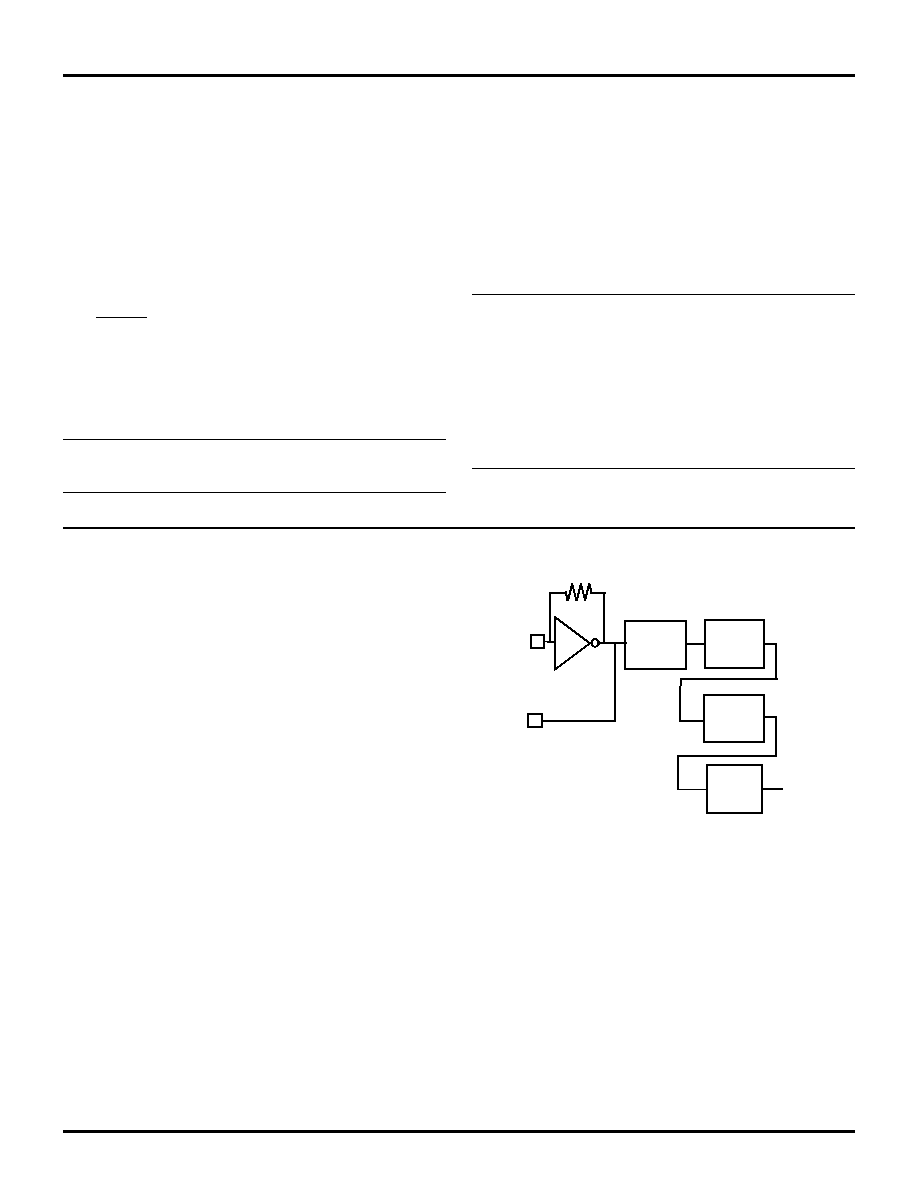
CLOCK
The Z8E001 MCU derives its timing from on-board clock
circuitry connected to pins XTAL1 and XTAL2. The clock
circuitry consists of an oscillator, a glitch filter, a divide-
by-two shaping circuit, a divide-by-four shaping circuit,
and a divide-by-eight shaping circuit. Figure 13 illustrates
the clock circuitry. The oscillator’s input is XTAL1 and its
output is XTAL2. The clock can be driven by a crystal, a
ceramic resonator, LC clock, or an external clock source.
6F
STOP
;enter STOP Mode
Figure 13. Z8E001 Clock Circuit
˜
2
XTAL2
XTAL1
Glitch
Filter
˜
4
˜
8
WDT
Clock
Timer
Clock
Machine
Clock
(5 cycles
per in-
struction)
Z8E001
Z8Plus OTP Microcontroller
ZiLOG
22
P R E L I M I N A R Y
DS001101-Z8X0400
OSCILLATOR OPERATION
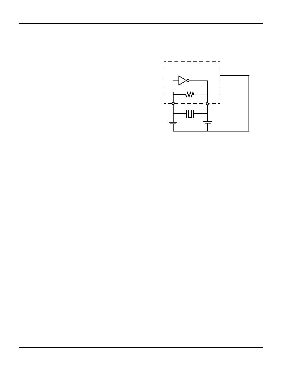
The Z8E001 MCU uses a Pierce oscillator with an internal
feedback resistor (Figure 14). The advantages of this circuit
are low-cost, large output signal, low-power level in the
crystal, stability with respect to V
CC
and temperature, and
low impedances (not disturbed by stray effects).
One draw back is the requirement for high gain in the am-
plifier to compensate for feedback path losses. The oscil-
lator amplifies its own noise at start-up until it settles at the
frequency that satisfies the gain/phase requirements (A x B
= 1; where A = V
o
/V
i
is the gain of the amplifier and B =
V
i
/V
o
is the gain of the feedback element). The total phase
shift around the loop is forced to zero (360 degrees). V
IN
must be in phase with itself; therefore, the amplifier/inverter
provides a 180-degree phase shift, and the feedback element
is forced to provide the other 180-degree phase shift.
R1 is a resistive component placed from output to input of
the amplifier. The purpose of this feedback is to bias the am-
plifier in its linear region and provide the start-up transition.
Capacitor C
2
, combined with the amplifier output resis-
tance, provides a small phase shift. It also provides some
attenuation of overtones.
Capacitor C
1
, combined with the crystal resistance, pro-
vides an additional phase shift.
C
1
and C
2
can affect the start-up time if they increase dra-
matically in size. As C
1
and C
2
increase, the start-up time
increases until the oscillator reaches a point where it does
not start up any more.
It is recommended for fast and reliable oscillator start-up
(over the manufacturing process range) that the load capac-
itors be sized as low as possible without resulting in over-
tone operation.
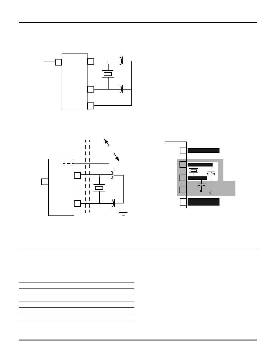
Layout
Traces connecting crystal, caps, and the Z8E001 oscillator
pins should be as short and wide as possible, to reduce par-
asitic inductance and resistance. The components (caps,
crystal, resistors) should be placed as close as possible to
the oscillator pins of the Z8E001.
The traces from the oscillator pins of the IC and the ground
side of the lead caps should be guarded from all other traces
(clock, V
CC
, address/data lines, system ground) to reduce
cross talk and noise injection. Guarding is usually accom-
plished by keeping other traces and system ground trace
planes away from the oscillator circuit, and by placing a
Z8E001 device V
SS
ground ring around the traces/compo-
nents. The ground side of the oscillator lead caps should be
connected to a single trace to the Z8E001 V
SS
(GND) pin.
It should not be shared with any other system ground trace
or components except at the Z8E001 device V
SS
pin. The
objective is to prevent differential system ground noise in-
jection into the oscillator (Figure 15).
Indications of an Unreliable Design
There are two major indicators that are used in working de-
signs to determine their reliability over full lot and temper-
ature variations. They are:
Start-up Time.
If start-up time is excessive, or varies wide-
ly from unit to unit, there is probably a gain problem. To
fix the problem, the capacitors C1/C2 require reduction.
The amplifier gain is either not adequate at frequency, or
the crystal Rs are too large.
Output Level.
The signal at the amplifier output should
swing from ground to V
CC
to indicate adequate gain in the
amplifier. As the oscillator starts up, the signal amplitude
grows until clipping occurs. At that point, the loop gain is
effectively reduced to unity, and constant oscillation is
achieved. A signal of less than 2.5 volts peak-to-peak is an
indication that low gain can be a problem. Either C
1
or C
2
should be made smaller, or a low-resistance crystal should
be used.
Circuit Board Design Rules
The following circuit board design rules are suggested:
•
To prevent induced noise, the crystal and load capacitors
should be physically located as close to the Z8E001 as
possible.
•
Signal lines should not run parallel to the clock oscillator
inputs. In particular, the crystal input circuitry and the in-
ternal system clock output should be separated as much
as possible.
Figure 14. Pierce Oscillator with Internal Feedback
Circuit
XTAL2
Z8E001
V
SS
XTAL1
C1
C2
R
I
V
1
A
V
0
Z8E001
ZiLOG
Z8Plus OTP Microcontroller
DS001101-Z8X0400
P R E L I M I N A R Y
23
•
V
CC
power lines should be separated from the clock os-
cillator input circuitry.
•
Resistivity between XTAL1 or XTAL2 (and the other
pins) should be greater than 10 M
.
Crystals and Resonators
Crystals and ceramic resonators (Figure 16) should have the
following characteristics to ensure proper oscillation:
Depending on the operation frequency, the oscillator can re-
quire additional capacitors, C1 and C2, as shown in Figure
16 and Figure 17. The capacitance values are dependent on
the manufacturer’s crystal specifications.
Figure 15. Circuit Board Design Rules
XTAL2
V
SS
XTAL1
Board Design Example
V
SS
Z8E001
Z8E001
Z8E001
C1
C2
Clock Generator Circuit
Signals A B
Signal C
(Parallel Traces
Must Be Avoided)
(Top View)
17
16
15
17
16
XTAL1
XTAL2
X1
X2
PB0
V
CC
Crystal Cut
AT (crystal only)
Mode
Parallel, Fundamental Mode
Crystal Capacitance
<7pF
Load Capacitance
10pF < CL < 220 pF,
15 typical
Resistance
100 ohms max
Z8E001
Z8Plus OTP Microcontroller
ZiLOG
24
P R E L I M I N A R Y
DS001101-Z8X0400
OSCILLATOR OPERATION (Continued)
In most cases, the R
D
is 0 Ohms and R
F
is infinite. These
specifications are determined and specified by the crys-
tal/ceramic resonator manufacturer. The R
D
can be in-
creased to decrease the amount of drive from the oscillator
output to the crystal. It can also be used as an adjustment
to avoid clipping of the oscillator signal to reduce noise. The
R
F
can be used to improve the start-up of the crystal/ceramic
resonator. The Z8E001 oscillator already has an internal
shunt resistor in parallel to the crystal/ceramic resonator.
Figure 16, Figure 17, and Figure 18 recommend that the
load capacitor ground trace connect directly to the V
SS
(GND) pin of the Z8E001. This requirement assures that no
system noise is injected into the Z8E001 clock. This trace
should not be shared with any other components except at
the V
SS
pin of the Z8E001.
Note: A parallel resonant crystal or resonator data sheet speci-
fies a load capacitor value that is a series combination of
C
1
and C
2
, including all parasitics (PCB and holder).
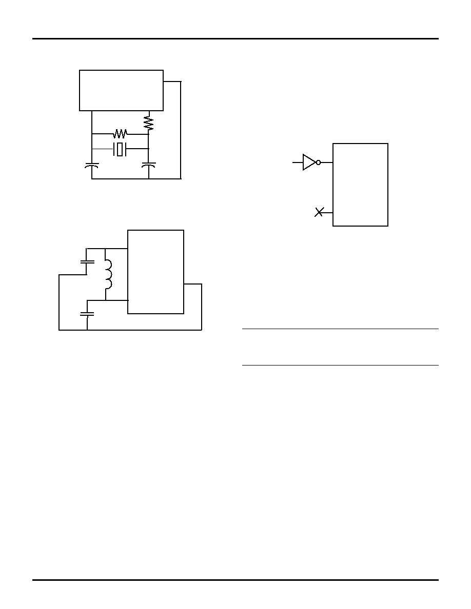
Figure 16. Crystal/Ceramic Resonator Oscillator
Figure 17. LC Clock
XTAL2
Z8E001
V
SS
XTAL1
C1
C2
R
F
R
D
XTAL2
Z8E001
V
SS
XTAL1
C1
C2
L
Figure 18. External Clock
XTAL2
Z8E001
V
SS
XTAL1
N/C
Z8E001
ZiLOG
Z8Plus OTP Microcontroller
DS001101-Z8X0400
P R E L I M I N A R Y
25
LC OSCILLATOR
The Z8E001 oscillator can use a LC network to generate a
XTAL clock (Figure 17).
The frequency stays stable over V
CC
and temperature. The
oscillation frequency is determined by the equation:
where L is the total inductance including parasitics, and C
T
is the total series capacitance including parasitics.
Simple series capacitance is calculated using the equation
at the top of the next column.
A sample calculation of capacitance C
1
and C
2
for 5.83
MHz frequency and inductance value of 27
µ
H is displayed
as follows:
TIMERS
For the Z8E001, 8-bit timers (T0 and T1) are available to
function as a pair of independent 8-bit standard timers, or
they can be cascaded to function as a 16-bit PWM timer.
In addition to T0 and T1, extra 8-bit timers (T2 and T3) are
provided, but they can only operate in cascade to function
as a 16-bit standard timer.
Frequency =
1
2
(
LC
T
)
1/2
1/ C
T
If C
1
1/C
T
C
1
=
=
=
=
1/C
1
+ 1/C
2
C
2
2 C
1
2C
T
5.83 (10^6) =
1
2
π
[2.7 (10
-6
) C
T
]
∫
C
T
= 27.6 pF
Thus C
1
= 55.2 pF and C
2
= 55.2 pF.
Figure 19. Z8E001 16-Bit Standard Timer
Enable TCTLL0 (D5)
IRQ5 (T23)
16-bit Down Counter
Internal Data Bus
T2VAL
T3VAL
OSC/8
T3AR
T2AR
Z8E001
Z8Plus OTP Microcontroller
ZiLOG
26
P R E L I M I N A R Y
DS001101-Z8X0400
TIMERS (Continued)
Figure 20. 8-Bit Standard Timers
Figure 21. 16-bit Standard PWM Timer
Enable TCTLL0 (D2-D0)
IRQ2 (T1)
Internal Data Bus
OSC/8
T1ARHI
T1ARLO
T1VAL
8-bit
Down
Counter
(Not used
in this mode)
8-bit Standard Tim
er
Enable TCTLL0 (D2-D0)
IRQ2 (T0)
Internal Data Bus
OSC/8
T0ARHI
T0ARLO
T0VAL
8-bit
Down
Counter
(Not used
in this mode)
8-bit Standard Tim
er
16-bit Down Counter
Internal Data Bus
High Side
PWM
Low Side
T1ARHI
T1ARLO
IRQ0
IRQ2
T1VAL
T1
T0
Internal Data Bus
T0ARHI
OSC/8
T0ARLO
T0VAL
Edge Detect
Logic
T
OUT
Z8E001
ZiLOG
Z8Plus OTP Microcontroller
DS001101-Z8X0400
P R E L I M I N A R Y
27
Each 8-bit timer is provided a pair of registers, which are
both readable and writable. One of the registers is defined
to contain the auto-initialization value for the timer, while
the second register contains the current value for the timer.
When a timer is enabled, the timer decrements whatever
value is currently held in its count register, and then con-
tinues decrementing until it reaches 0. At this time, an in-
terrupt is generated and the contents of the auto-initializa-
tion register optionally copy into the count value register.
If auto-initialization is not enabled, the timer stops counting
upon reaching 0, and control logic clears the appropriate
control register bit to disable the timer. This operation is re-
ferred to as “single-shot”. If auto-initialization is enabled,
the timer continues counting from the initialization value.
Software should not attempt to use registers that are defined
as having timer functionality.
Software is allowed to write to any register at any time, but
care should be taken if timer registers are updated while the
timer is enabled. If software updates the count value while
the timer is in operation, the timer continues counting based
upon the software-updated value.
Note: Strange behavior can result if the software update oc-
curred at exactly the point that the timer was reaching 0
to trigger an interrupt and/or reload.
Similarly, if software updates the initialization value reg-
ister while the timer is active, the next time that the timer
reaches 0, it initializes using the updated value.
Note: Strange behavior could result if the initialization value
register is being written while the timer is in the process
of being initialized.
Whether initialization is done with the new or old value is
a function of the exact timing of the write operation. In all
cases, the Z8E001 prioritizes the software write above that
of a decrementer writeback; however, when hardware
clears a control register bit for a timer that is configured for
single-shot operation, the clearing of the control bit over-
rides a software write. Reading either register can be done
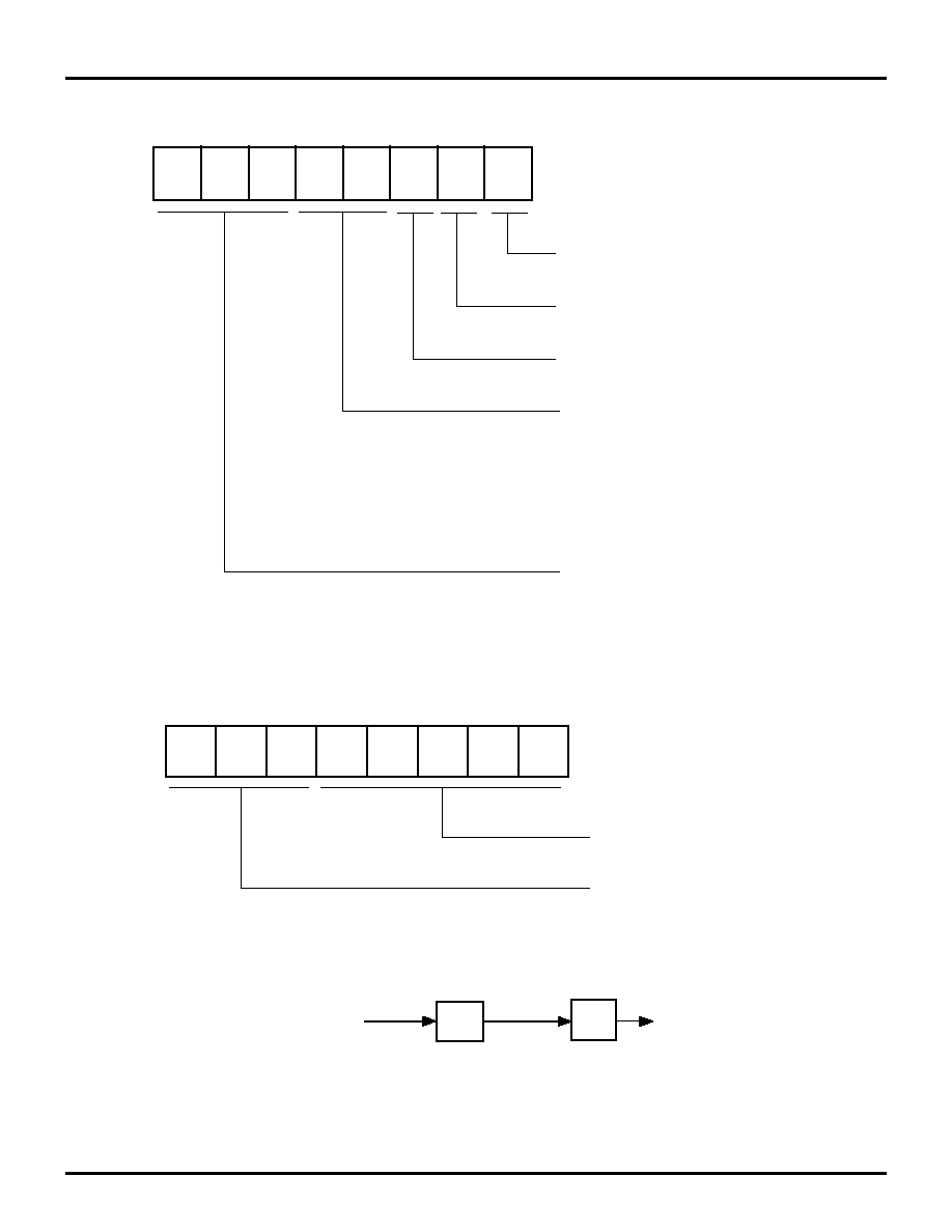
Figure 22. TCTLLO Register
D7
D6
D5
D4
D3
D2
D1
D0
0C0
TCTLLO
TIMER STATUS
D2 D1 D0 T0 T1 T01
---- ---- --- ------------ ------------ ---------------
0 0 0 DISAB. DISAB.
0 0 1 ENAB. DISAB.
0 1 0 DISAB. ENAB.
0 1 1 ENAB. ENAB.
1 0 0 ENAB.(*)
1 0 1 ENAB.(*) DISAB.
1 1 0 DISAB. ENAB.(*)
1 1 1 ENAB.(*) ENAB.(*)
(NOTE: (*) INDICATES AUTO-RELOAD
IS ACTIVE.)
RESERVED (MUST BE 0)
1 = T23 16-BIT TIMER ENABLED WITH
AUTO-RELOAD ACTIVE
0 = T2 AND T3 TIMERS DISABLED
RESERVED (MUST BE 0)
Note: Timer T01 is a 16-bit PWM Timer formed by cascading 8-bit timers
T1 (MSB) and T0 (LSB). T23 is a standard 16-bit timer formed
by cascading 8-bit timers T3 (MSB) and T2 (LSB).

Z8E001
Z8Plus OTP Microcontroller
ZiLOG
28
P R E L I M I N A R Y
DS001101-Z8X0400
TIMERS (Continued)
at any time, and will have no effect on the functionality of
the timer.
If a timer pair is defined to operate as a single 16-bit entity,
the entire 16-bit value must reach 0 before an interrupt is
generated. In this case, a single interrupt is generated, and
the interrupt corresponds to the even 8-bit timer.
Example: Timers T2 and T3 are cascaded to form a single 16-
bit timer, so the interrupt for the combined timer is
defined to be that of timer T2 rather than T3. When
a timer pair is specified to act as a single 16-bit
timer, the even timer registers in the pair (timer T0
or T2) is defined to hold the timer’s least significant
byte. In contrast, the odd timer in the pair holds the
timer’s most significant byte.
In parallel with the posting of the interrupt request, the in-
terrupting timer’s count value is initialized by copying the
contents of the auto-initialization value register to the count
value register. It should be noted that any time that a timer
pair is defined to act as a single 16-bit timer, that the auto-
reload function is performed automatically. All 16-bit tim-
ers continue counting while their interrupt requests are ac-
tive, and each operates in a free-running manner.
If interrupts are disabled for a long period of time, it is pos-
sible for the timer to decrement to 0 again before its initial
interrupt has been responded to. This condition is termed a
degenerate case, and hardware is not required to detect it.
When the timer control register is written, all timers that are
enabled by the write begins counting using the value that
is held in the count register. In this case, an auto-initializa-
tion is not performed. All timers can receive an internal
clock source only. Each timer that is enabled is updated ev-
ery 8th XTAL clock cycle.
If T0 and T1 are defined to work independently, then each
works as an 8-bit timer with a single auto-initialization reg-
ister (T0ARLO for T0, and T1ARLO for T1). Each timer
asserts its predefined interrupt when it times out, optionally
performing the auto-initialization function. If T0 and T1 are
cascaded to form a single 16-bit timer, then the single 16-
bit timer is capable of performing as a Pulse-Width Mod-
ulator (PWM). This timer is referred to as T01 to distinguish
it as having special functionality that is not available when
T0 and T1 act independently.
When T01 is enabled, it can use a pair of 16-bit auto-ini-
tialization registers. In this mode, one 16-bit auto-initial-
ization value is composed of the concatenation of T1ARLO
and T0ARLO. The second auto-initialization value is com-
posed of the concatenation of T1ARHI and T0ARHI. When
T01 times out, it alternately initializes its count value using
the LO auto-init pair, followed by the HI auto-init pair. This
functionality corresponds to a PWM, where the T1 interrupt
defines the end of the HI section of the waveform, and the
T0 interrupt marks the end of the LO portion of the PWM
waveform.
To use the cascaded timers as a PWM, one must initialize
the T0 and T1 count registers to work in conjunction with
the port pin. The user should initialize the T0 and T1 count
registers to the PWM_HI auto-init value to obtain the re-
quired PWM behavior. The PWM is arbitrarily defined to
use the LO autoreload registers first, implying that it had
just timed out after beginning in the HI portion of the PWM
waveform. As such, the PWM is defined to assert the T1
interrupt after the first timeout interval.
After the auto-initialization has been completed, decre-
menting occurs for the number of counts defined by the
PWM_LO registers. When decrementing again reaches 0,
the T0 interrupt is asserted; and auto-init using the
PWM_HI registers occurs. Decrementing occurs for the
number of counts defined by the PWM_HI registers until
reaching 0. From there, the T1 interrupt is asserted, and the
cycle begins again.
The internal timers can be used to trigger external events
by toggling the PB1 output when generating an interrupt.
This functionality can only be achieved in conjunction with
the port unit defining the appropriate pin as an output signal
with the timer output special function enabled. In this mode,
the appropriate port output is toggled when the timer count
reaches 0, and continues toggling each time that the timer
times out.
T
OUT
Mode
The PortB special function register PTBSFR (0D7H) (Fig-
ure 23) is used in conjunction with the Port B directional
control register PTBDIR (0D6) (Figure 24) to configure
PB1 for T
OUT
operation for timer0. In order for T
OUT
to
function, PB1 must be defined as an output line by setting
PTBDIR bit 1 to 1. Configured in this way, PB1 has the ca-
pability of being a clock output for timer0, toggling the PB1
output pin on each timer0 timeout.
At end-of-count, the interrupt request line IRQ0, clocks a
toggle flip-flop. The output of this flip-flop drives the T
OUT
line, PB1. In all cases, when timer0 reaches its end-of-count,
T
OUT
toggles to its opposite state (Figure 25). If, for ex-
ample, timer0 is in Continuous Counting Mode, T
OUT
has
a 50 percent duty cycle output. This duty cycle can easily
be controlled by varying the initial values after each end-
of-count.
Z8E001
ZiLOG
Z8Plus OTP Microcontroller
DS001101-Z8X0400
P R E L I M I N A R Y
29
Figure 23. PortB Special Function Register (T
out
Operation)
Figure 24. Port B Directional Control Register
Figure 25. Timer T0 Output Through T
OUT
D7
D6
D5
D4
D3
D2
D1
D0
0D7
PTBSFR
1 = ENABLE BIT 0 AS SMR INPUT
0 = NO SPECIAL FUNCTIONALITY
1 = ENABLE BIT 1 AS TIMER0 OUTPUT
0 = NO SPECIAL FUNCTIONALITY
1 = ENABLE BIT 2 AS INT1 INPUT
0 = NO SPECIAL FUNCTIONALITY
D4 D3 COMPAR. INTERRUPTS
--- --- -------------- -------------------
0 0 DISABLED DISABLED
0 1 ENABLED DISABLED
1 0 DISABLED ENABLED
1 1 ENABLED ENABLED
BIT 3: COMP. REF. INPUT
BIT 4: COMP. SIGNAL INPUT/
INT0/INT2
RESERVED (MUST BE 0)
D7
D6
D5
D4
D3
D2
D1
D0
0D6
PTBDIR
RESERVED (MUST BE 0)
1 = BIT N SET AS OUTPUT
0 = BIT N SET AS INPUT
T
OUT
PB1
IRQ0
(T0
End-of-Count)
˜
2

Z8E001
Z8Plus OTP Microcontroller
ZiLOG
30
P R E L I M I N A R Y
DS001101-Z8X0400
RESET CONDITIONS
After a hardware RESET, the timers are disabled. See Table
4 for timer control, value, and auto-initialization register
status after RESET.
I/O PORTS
The Z8E001 has 13 lines dedicated to input and output.
These lines are grouped into two ports known as Port A and
Port B. Port A is an 8-bit port, bit programmable as either
inputs or outputs. Port B can be programmed to provide
standard input/output or the following special functions:
timer0 output, comparator input, SMR input, and external
interrupt inputs.
All ports have push-pull CMOS outputs. In addition, the
outputs of Port A on a bit-wise basis can be configured for
open-drain operation.The ports operate on a bit-wise basis.
As such, the register values for/at a given bit position only
affect the bit in question.
Each port is defined by a set of four control registers. See
Figure 27.
Directional Control and Special Function
Registers
Each port on the Z8E001 has a dedicated Directional Con-
trol Register that determines (on a bit-wise basis) whether
a given port bit operates as either an input or an output.
Each port on the Z8E001 has a Special Function Register
that, in conjunction with the Directional Control Register,
implements (on a bit-wise basis), any special functionality
that can be defined for each particular port bit.
Input and Output Value Registers
Each port has an Output Value Register and a pF Input Val-
ue Register. For port bits configured as an input by means
of the Directional Control Register, the Input Value Reg-
ister for that bit position contains the current synchronized
input value.
For port bits configured as an output by means of the Di-
rectional Control Register, the value held in the correspond-
ing bit of the Output Value Register is driven directly onto
the output pin. The opposite register bit for a given pin (the
output register bit for an input pin and the input register bit
for an output pin) holds their previous value. These bits are
not changed and don’t have any effect on the hardware.
READ/WRITE OPERATIONS
The control for each port is done on a bit-wise basis. All
bits are capable of operating as inputs or outputs, depending
upon the setting of the port’s Directional Control Register.
If configured as an input, each bit is provided a Schmitt-
trigger. The output of the Schmitt-trigger is latched twice
to perform a synchronization function, and the output of the
synchronizer is fed to the port input register, which can be
read by software.
A write to a port input register has the effect of updating
the contents of the input register, but subsequent reads do
not necessarily return the same value that was written. If the
bit in question is defined as an input, the input register for
that bit position contains the current synchronized input val-
ue. Thus, writes to that bit position is overwritten on the next
clock cycle with the newly sampled input data. However,
if the particular port bit is programmed as an output, the in-
put register for that bit retains the software-updated value.
The port bits that are programmed as outputs do not sample
the value being driven out.
Any bit in either port can be defined as an output by setting
the appropriate bit in the directional control register. If such
is the case, the value held in the appropriate bit of the port
output register is driven directly onto the output pin.
Table 7. Z8E001 I/O Ports Registers
Register
Address
Identifier
Port B Special Function
OD7H
PTBSFR
Port B Directional Control
0D6H
PTBDIR
Port B Output Value
0D5H
PTBOUT
Port B Input Value
0D4H
PTBIN
Port A Special Function
0D3H
PTASFR
Port A Directional Control
0D2H
PTADIR
Port A Output Value
0D1H
PTAOUT
Port A Input Value
0D0H
PTAIN
Z8E001
ZiLOG
Z8Plus OTP Microcontroller
DS001101-Z8X0400
P R E L I M I N A R Y
31
Note: The preceding result does not necessarily reflect the ac-
tual output value. If an external error is holding an output
pin either High or Low against the output driver, the soft-
ware read returns the required value, not the actual state
caused by the contention. When a bit is defined as an out-
put, the Schmitt-trigger on the input is disabled to save
power.
Updates to the output register takes effect based upon the
timing of the internal instruction pipeline, but is referenced
to the rising edge of the clock. The output register can be
read at any time, and returns the current output value that
is held. No restrictions are placed on the timing of reads
and/or writes to any of the port registers with respect to the
others; however, care should be taken when updating the
directional control and special function registers.
When updating a Directional Control Register, the Special
Function Register should first be disabled. If this precaution
is not taken, spurious events could take place as a result of
the change in port I/O status. This precaution is especially
important when defining changes in Port B, as the spurious
event referred to above could be one or more interrupts.
Clearing of the SFR register should be the first step in con-
figuring the port, while setting the SFR register should be
the final step in the port configuration process. To ensure
deterministic behavior, the SFR register should not be writ-
ten until the pins are being driven appropriately, and all ini-
tialization has been completed.
PORT A
Port A is a general-purpose port. Figure 26 features a block
diagram of Port A. Each of its lines can be independently
programmed as input or output via the Port A Directional
Control Register (PTADIR at 0D2H) as seen in Figure 27.
A bit set to a 1 in PTADIR configures the corresponding
bit in Port A as an output, while a bit cleared to 0 configures
the corresponding bit in Port A as an input.
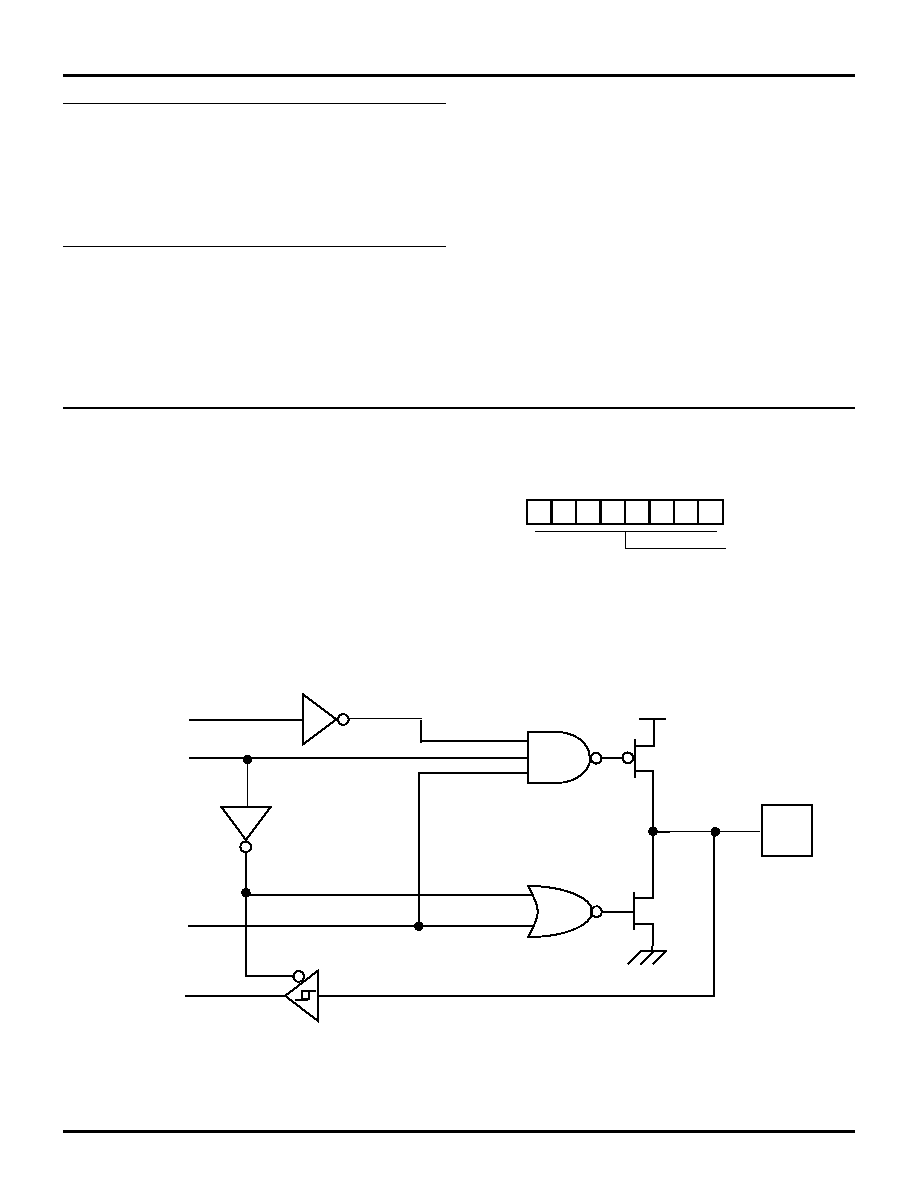
The input buffers are Schmitt-triggered. Bits programmed
as outputs can be individually programmed as either push-
pull or open drain by setting the corresponding bit in the
Special Function Register (PTASFR, Figure 27).
Figure 26. Port A Directional Control Register
D7 D6 D5 D4 D3 D2 D1 D0
0 = Input
1 = Output
PTADIR Register
Register 0D2H
Figure 27. Port A Configuration with Open-Drain Capability and Schmitt-Trigger
PIN
PA0–PA7
PTAIN.bitN
N = 0...7
PTAOUT.bitN
N = 0...7
PTASFR.bitN
N = 0...7
PTADIR.bitN
N = 0...7
Z8E001
Z8Plus OTP Microcontroller
ZiLOG
32
P R E L I M I N A R Y
DS001101-Z8X0400
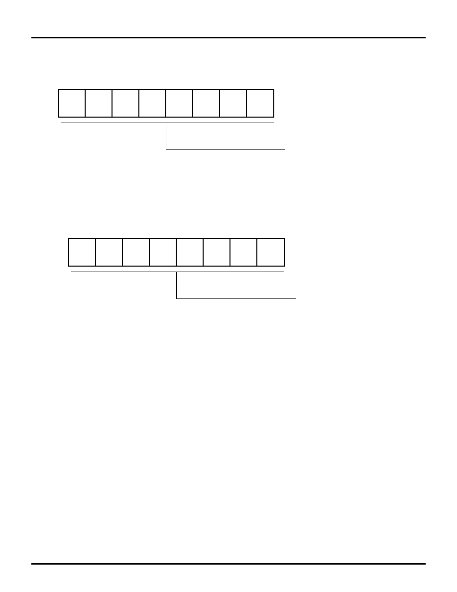
PORT A REGISTER DIAGRAMS
Figure 28. Port A Input Value Register
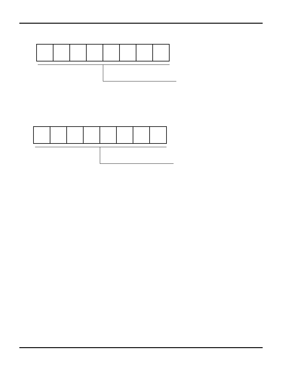
Figure 29. Port A Output Value Register
D7
D6
D5
D4
D3
D2
D1
D0
Register 0D0H
PTAIN
PORT A BIT N CURRENT INPUT
VALUE
(only updated for pins in
input mode)
D7
D6
D5
D4
D3
D2
D1
D0
Register 0D1H
PTAOUT
PORT A BIT N CURRENT
OUTPUT VALUE
Z8E001
ZiLOG
Z8Plus OTP Microcontroller
DS001101-Z8X0400
P R E L I M I N A R Y
33
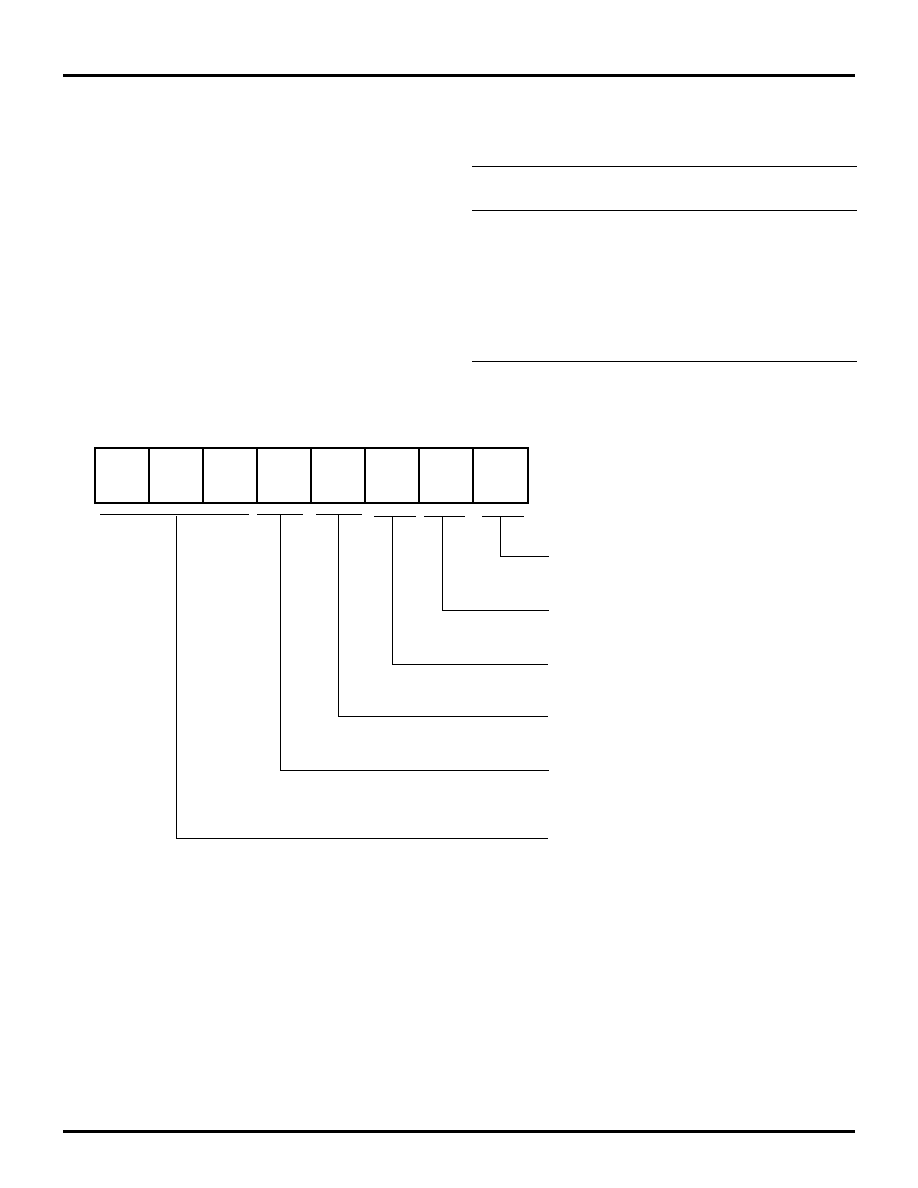
Figure 30. Port A Directional Control Register
Figure 31. Port A Special Function Register
D7
D6
D5
D4
D3
D2
D1
D0
Register 0D2H
PTADIR
1 = BIT N SET AS AN OUTPUT
0 = BIT N SET AS AN INPUT
D7
D6
D5
D4
D3
D2
D1
D0
Register 0D3H
PTASFR
1 = BIT N IN OPEN-DRAIN MODE
0 = BIT N IN PUSH-PULL MODE
Z8E001
Z8Plus OTP Microcontroller
ZiLOG
34
P R E L I M I N A R Y
DS001101-Z8X0400
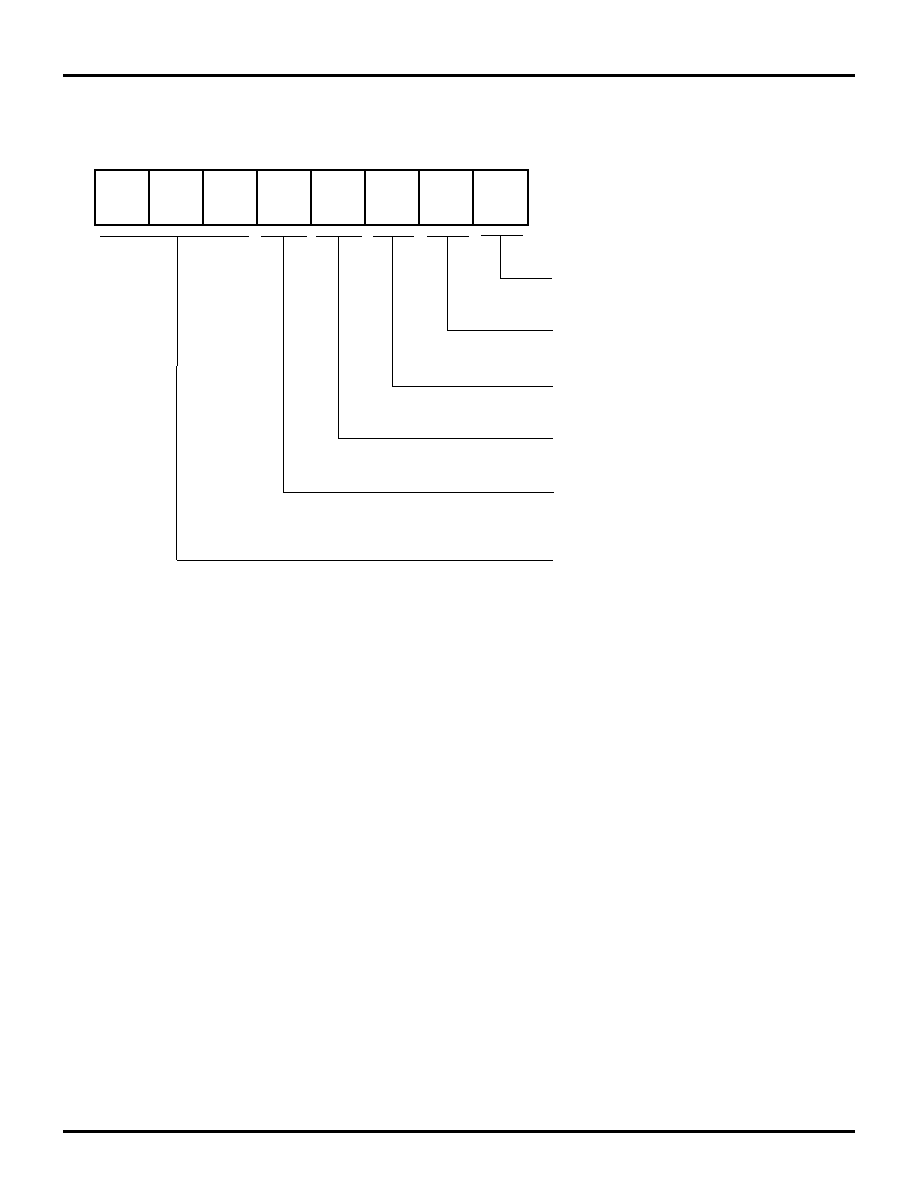
PORT B
Port B Description
Port B is a 5-bit (bidirectional), CMOS-compatible I/O port.
These five I/O lines can be configured under software con-
trol to be an input or output, independently. Input buffers
are Schmitt-triggered. See Figure 33 through Figure 36 for
diagrams of all five Port B pins.
In addition to standard input/output capability on all five
pins of Port B, each pin provides special functionality as
shown in the following table:
Special functionality is invoked via the Port B Special Func-
tion Register. See Figure 32 for the arrangement and control
conventions of this register.
Table 8. Port B Special Functions
Port Pin
Input Special
Function
Output Special
Function
PB0
Stop Mode Recovery
Input
None
PB1
None
Timer0 Output
PB2
IRQ3
None
PB3
Comparator Reference
Input
None
PB4
Comparator Signal
Input/IRQ1/IRQ4
None
Figure 32. Port B Special Function Register
D7
D6
D5
D4
D3
D2
D1
D0
Register 0D7H
PTBSFR
1 = ENABLE PB0 AS SMR INPUT
0 = NO SPECIAL FUNCTIONALITY
1 = ENABLE PB1 AS TIMER0 OUTPUT
0 = NO SPECIAL FUNCTIONALITY
1 = ENABLE PB2 AS IRQ3 INPUT
0 = NO SPECIAL FUNCTIONALITY
RESERVED (MUST BE 0)
1 = Analog Comparator on PB3 & PB4
0 = Digital Inputs on PB3 & PB4
1 = PB4 Interrupts Enabled
0 = PB4 Interrupts Disabled
Z8E001
ZiLOG
Z8Plus OTP Microcontroller
DS001101-Z8X0400
P R E L I M I N A R Y
35
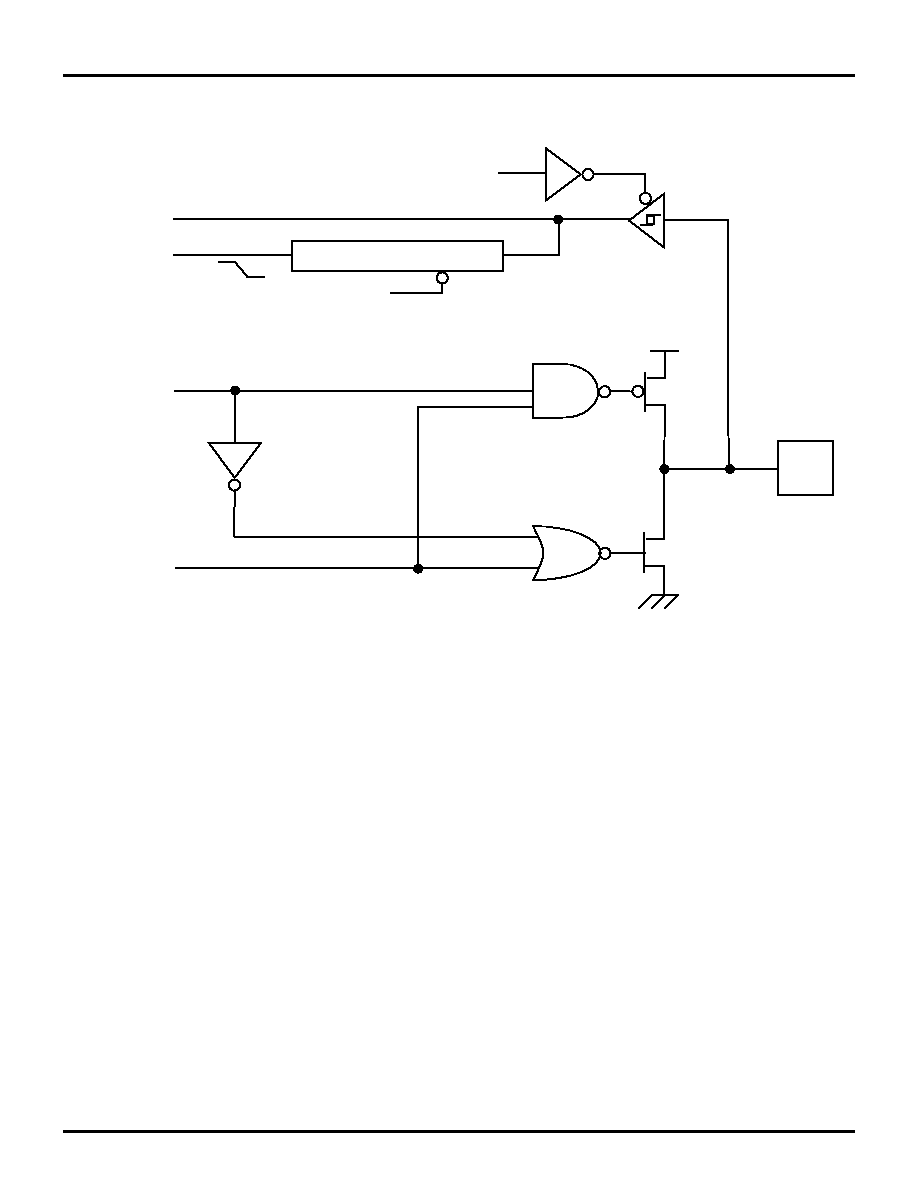
PORT B—PIN 0 CONFIGURATION
Figure 33. Port B Pin 0 Diagram
PIN
PB0
PTBOUT.bit0
PTBSFR.bit0
PTBDIR.bit0
PTBDIR.bit0
PTBIN.bit0
SMR
SMR Flag
RESET
Z8E001
Z8Plus OTP Microcontroller
ZiLOG
36
P R E L I M I N A R Y
DS001101-Z8X0400
PORT B—PIN 1 CONFIGURATION
Figure 34. Port B Pin 1 Diagram
PIN
PB1
TIMER0
PTBOUT.bit1
PTBSFR.bit1
PTBDIR.bit1
PTBDIR.bit1
PTBIN.bit1
Output
M
U
X
Z8E001
ZiLOG
Z8Plus OTP Microcontroller
DS001101-Z8X0400
P R E L I M I N A R Y
37
PORT B—PIN 2 CONFIGURATION
Figure 35. Port B Pin 2 Diagram
PIN
PB2
PTBOUT.bit2
PTBSFR.bit2
PTBDIR.bit2
PTBDIR.bit2
PTBIN.bit2
EDGE DETECT LOGIC
IRQ3
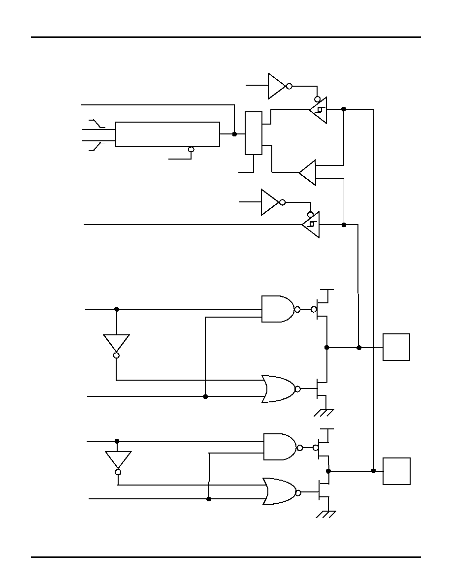
Z8E001
Z8Plus OTP Microcontroller
ZiLOG
38
P R E L I M I N A R Y
DS001101-Z8X0400
PORT B—PINS 3 AND 4 CONFIGURATION
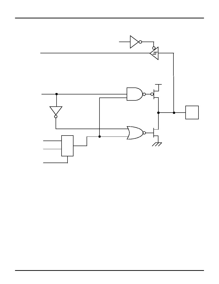
Figure 36. Port B Pins 3 and 4 Diagram
PIN
PB3
PTBOUT.bit3
PTBSFR.bit3
PTBDIR.bit3
PTBDIR.bit4
PTBIN.bit4
EDGE DETECT LOGIC
IRQ1
IRQ4
+
AN IN
REF
PTBDIR.bit3
PTBIN.bit3
PIN
PB4
PTBOUT.bit4
PTBDIR.bit4
PTBSFR.bit4
M
U
X
-
Z8E001
ZiLOG
Z8Plus OTP Microcontroller
DS001101-Z8X0400
P R E L I M I N A R Y
39
PORT B CONTROL REGISTERS
Figure 37. Port B Input Value Register
Figure 38. Port B Output Value Register
Figure 39. Port B Directional Control Register
D7
D6
D5
D4
D3
D2
D1
D0
Register 0D4H
PTBIN
PORT B BIT N CURRENT INPUT
VALUE
RESERVED (MUST BE 0)
(only updated for pins in
input mode)
D7
D6
D5
D4
D3
D2
D1
D0
Register 0D5H
PTBOUT
PORT B BIT N CURRENT
OUTPUT VALUE
RESERVED (MUST BE 0)
D7
D6
D5
D4
D3
D2
D1
D0
Register 0D6H
PTBDIR
RESERVED (MUST BE 0)
1 = BIT N SET AS OUTPUT
0 = BIT N SET AS INPUT
Z8E001
Z8Plus OTP Microcontroller
ZiLOG
40
P R E L I M I N A R Y
DS001101-Z8X0400
PORT B CONTROL REGISTERS (Continued)
Figure 40. Port B Special Function Register
D7
D6
D5
D4
D3
D2
D1
D0
Register 0D7H
PTBSFR
1 = ENABLE PB0 AS SMR INPUT
0 = NO SPECIAL FUNCTIONALITY
1 = ENABLE PB1 AS TIMER0 OUTPUT
0 = NO SPECIAL FUNCTIONALITY
1 = ENABLE PB2 AS IRQ3 INPUT
0 = NO SPECIAL FUNCTIONALITY
RESERVED (MUST BE 0)
1 = Analog Comparator on PB3 & PB4
0 = Digital Inputs on PB3 & PB4
1 = PB4 Interrupts Enabled
0 = PB4 Interrupts Disabled

Z8E001
ZiLOG
Z8Plus OTP Microcontroller
DS001101-Z8X0400
P R E L I M I N A R Y
41
I/O PORT RESET CONDITIONS
Full Reset
Port A and Port B output value registers are not affected by
RESET.
On RESET, the Port A and Port B directional control reg-
isters is cleared to all zeros, which defines all pins in both
ports as inputs.
On RESET, the directional control registers redefine all
pins as inputs, and the Port A and Port B input value registers
overwrites the previously held data with the current sample
of the input pins.
On RESET, the Port A and Port B special function registers
is cleared to all zeros, which deactivates all port special
functions.
Note: The SMR and WDT timeout events are NOT full device
resets. The port control registers are not affected by ei-
ther of these events.
ANALOG COMPARATOR
The Z8E001 includes one on-chip analog comparator. Pin
PB4 has a comparator front end. The comparator reference
voltage is on pin PB3.
Comparator Description
The on-chip comparator can process an analog signal on
PB4 with reference to the voltage on PB3. The analog func-
tion is enabled by programming the Port B Special Function
Register bits 3 and 4.
When the analog comparator function is enabled, bit 4 of
the input register is defined as holding the synchronized out-
put of the comparator, while bit 3 retains a synchronized
sample of the reference input.
If the interrupts for PB4 are enabled when the comparator
special function is selected, the output of the comparator
generates interrupts.
COMPARATOR OPERATION
The comparator output reflects the relationship between the
analog input to the reference input. If the voltage on the an-
alog input is higher than the voltage on the reference input,
then the comparator output is at a High state. If the voltage
on the analog input is lower than the voltage on the reference
input, then the analog output will be at a Low state.
Comparator Definitions
V
ICR
The usable voltage range for the positive input and reference
input is called the common mode voltage range (V
ICR
).
Note: The comparator is not guaranteed to work if the input is
outside of the V
ICR
range.
V
OFFSET
The absolute value of the voltage between the positive input
and the reference input required to make the comparator
output voltage switch is the input offset voltage (V
OFFSET
).
I
IO
For the CMOS voltage comparator input, the input offset
current (I
IO
) is the leakage current of the CMOS input gate.
HALT Mode
The analog comparator is functional during HALT Mode.
If the interrupts are enabled, an interrupt generated by the
comparator will cause a return from HALT Mode.
STOP Mode
The analog comparator is disabled during STOP Mode. The
comparator is powered down to prevent it from drawing any
current.
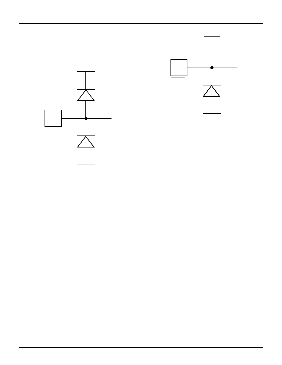
Z8E001
Z8Plus OTP Microcontroller
ZiLOG
42
P R E L I M I N A R Y
DS001101-Z8X0400
INPUT PROTECTION
All I/O pins on the Z8E001 have diode input protection.
There is a diode from the I/O pad to V
CC
and V
SS
(Figure
41).
However, on the Z8E001, the RESET pin has only the input
protection diode from pad to V
SS
(Figure 42).
The high-side input protection diode was removed on this
pin to allow the application of high voltage during the OTP
programming mode.
For better noise immunity in applications that are exposed
to system EMI, a clamping diode to V
CC
from this pin can
be required to prevent entering the OTP programming mode
or to prevent high voltage from damaging this pin.
Figure 41. I/O Pin Diode Input Protection
PIN
V
CC
V
SS
Figure 42. RESET Pin Input Protection
PIN
V
SS
RESET
Z8E001
ZiLOG
Z8Plus OTP Microcontroller
DS001101-Z8X0400
P R E L I M I N A R Y
43
PACKAGE INFORMATION
Figure 43. 18-Pin DIP Package Diagram
Figure 44. 18-Pin SOIC Package Diagram
Z8E001
Z8Plus OTP Microcontroller
ZiLOG
44
P R E L I M I N A R Y
DS001101-Z8X0400
PACKAGE INFORMATION (Continued)
Figure 45. 20-Pin SSOP Package Diagram

Z8E001
ZiLOG
Z8Plus OTP Microcontroller
DS001101-Z8X0400
P R E L I M I N A R Y
45
ORDERING INFORMATION
For fast results, contact your local ZiLOG sales office for
assistance in ordering the part(s) required.
Standard Temperature
18-Pin DIP
Z8E00110SSC
18-Pin SOIC
Z8E00110HSC
20-Pin SSOP
Z8E00110PSC
Extended Temperature
18-Pin DIP
Z8E00110PEC
18-Pin SOIC
Z8E00110SEC
20-Pin SSOP
Z8E00110HEC
Codes
Preferred Package
P = Plastic DIP
Longer Lead Time
S = SOIC
H = SSOP
Preferred Temperature S = 0°C to +70°C
E = –40°C to +105°C
Speed
10 = 10 MHz
Environmental
C = Plastic Standard
Example:
Z 8E001 10 P S C is a Z86E001, 10 MHz, DIP, 0° to +70°C, Plastic Standard Flow
Environmental Flow
Temperature
Package
Speed
Product Number
ZiLOG Prefix

Z8E001
Z8Plus OTP Microcontroller
ZiLOG
46
P R E L I M I N A R Y
DS001101-Z8X0400
Pre-Characterization Product:
The product represented by this document is newly introduced
and ZiLOG has not completed the full characterization of the
product. The document states what ZiLOG knows about this
product at this time, but additional features or non-conformance
with some aspects of the document may be found, either by
ZiLOG or its customers in the course of further application and
characterization work. In addition, ZiLOG cautions that delivery
may be uncertain at times, due to start-up yield issues.
Development Projects:
Customer is cautioned that while reasonable efforts will be
employed to meet performance objectives and milestone dates,
development is subject to unanticipated problems and delays.
No production release is authorized or committed until the
Customer and ZiLOG have agreed upon a Product Specification
for this project.
Low Margin:
Customer is advised that this product does not meet ZiLOG's
internal guardbanded test policies for the specification requested
and is supplied on an exception basis. Customer is cautioned that
delivery may be uncertain and that, in addition to all other
limitations on ZiLOG liability stated on the front and back of the
acknowledgement, ZiLOG makes no claim as to quality and
reliability under the document. The product remains subject to
standard warranty for replacement due to defects in materials
and workmanship.
©1999 by ZiLOG, Inc. All rights reserved. Information in this
publication concerning the devices, applications, or technology
described is intended to suggest possible uses and may be
superseded. ZiLOG, INC. DOES NOT ASSUME LIABILITY
FOR OR PROVIDE A REPRESENTATION OF ACCURACY
OF THE INFORMATION, DEVICES, OR TECHNOLOGY
DESCRIBED IN THIS DOCUMENT. ZiLOG ALSO DOES
NOT ASSUME LIABILITY FOR INTELLECTUAL
PROPERTY INFRINGEMENT RELATED IN ANY
MANNER TO USE OF INFORMATION, DEVICES, OR
TECHNOLOGY DESCRIBED HEREIN OR OTHERWISE.
Except with the express written approval of ZiLOG, use of
information, devices, or technology as critical components of
life support systems is not authorized. No licenses are conveyed,
implicitly or otherwise, by this document under any intellectual
property rights.
ZiLOG, Inc.
910 East Hamilton Avenue, Suite 110
Campbell, CA 95008
Telephone (408) 558-8500
FAX 408 558-8300
Internet:
http://www.zilog.com