
Product Specification
High Performance 8-Bit Microcontrollers
Z8 Encore!
�
64K Series
ZiLOG Worldwide Headquarters � 532 Race Street � San Jose, CA 95126-3432
Telephone: 408.558.8500 � Fax: 408.558.8300 �
www.ZiLOG.com
PS019915-1005

PS019915-1005
This publication is subject to replacement by a later edition. To determine whether
a later edition exists, or to request copies of publications, contact:
ZiLOG Worldwide Headquarters
532 Race Street
San Jose, CA 95126
Telephone: 408.558.8500
Fax: 408.558.8300
www.ZiLOG.com
Document Disclaimer
ZiLOG is a registered trademark of ZiLOG Inc. in the United States and in other countries. All other
products and/or service names mentioned herein may be trademarks of the companies with which
they are associated.
�2005 by ZiLOG, Inc. All rights reserved. Information in this publication concerning the devices,
applications, or technology described is intended to suggest possible uses and may be superseded.
ZiLOG, INC. DOES NOT ASSUME LIABILITY FOR OR PROVIDE A REPRESENTATION OF
ACCURACY OF THE INFORMATION, DEVICES, OR TECHNOLOGY DESCRIBED IN THIS
DOCUMENT. ZiLOG ALSO DOES NOT ASSUME LIABILITY FOR INTELLECTUAL PROPERTY
INFRINGEMENT RELATED IN ANY MANNER TO USE OF INFORMATION, DEVICES, OR
TECHNOLOGY DESCRIBED HEREIN OR OTHERWISE. Devices sold by ZiLOG, Inc. are covered
by warranty and limitation of liability provisions appearing in the ZiLOG, Inc. Terms and Conditions of
Sale. ZiLOG, Inc. makes no warranty of merchantability or fitness for any purpose Except with the
express written approval of ZiLOG, use of information, devices, or technology as critical components
of life support systems is not authorized. No licenses are conveyed, implicitly or otherwise, by this
document under any intellectual property rights.

PS019915-1005
Z8 Encore!
�
64K Series
Product Specification
iii
Revision History
Each instance in Table 1 reflects a change to this document from its previous revi-
sion. To see more detail, click the appropriate link in the table.
Table 1. Revision History of this Document
Date
Revision
Level
Description
Page #
January
2005
12
Added Die Form Sales information to Table 1.
2
March
2005
13
Provided timing equation when the Baud Rate Generator for a
peripheral is used as a simple timer. Closes CR#5618.
109, 115,
131, 137,
155
August
2005
14
Updated "Manual Objectives" on page xviii, "Introduction" on page 1, "Available
Packages" on page 6, "Program Memory" on page 18, "Flash Memory" on
page 178, "Option Bits" on page 190, "On-Chip Debugger Commands" on
page 198, "Absolute Maximum Ratings" on page 209, "DC Characteristics" on
page 211, Figure 48 on page 218, "On-Chip Peripheral AC and DC Electrical
Characteristics" on page 219, "AC Characteristics" on page 224, "Ordering
Information" on page 262, and "Part Number Suffix Designations" on page 267.
Removed "Preliminary" from all pages. Deleted first sentence of "Electrical
Characteristics" chapter. Deleted "Precharacterization Product" section in the
"Packaging" chapter. Added automotive/industrial parts; removed all ROM
references.
October
2005
15
The paragraph tag for "Ordering Information" has been changed from
H1 Heading to Chapter Title.
262

PS019915-1005
Table of Contents
Z8 Encore!
�
64K Series
Product Specification
iv
Table of Contents
Revision History . . . . . . . . . . . . . . . . . . . . . . . . . . . . . . . . . . . . . . . . . . . . . . . . . . . . . . . .iii
Table of Contents . . . . . . . . . . . . . . . . . . . . . . . . . . . . . . . . . . . . . . . . . . . . . . . . . . . . . . . . . . iv
List of Figures . . . . . . . . . . . . . . . . . . . . . . . . . . . . . . . . . . . . . . . . . . . . . . . . . . . . . . . . . . . . . xi
List of Tables . . . . . . . . . . . . . . . . . . . . . . . . . . . . . . . . . . . . . . . . . . . . . . . . . . . . . . . . . . . . xiv
Manual Objectives . . . . . . . . . . . . . . . . . . . . . . . . . . . . . . . . . . . . . . . . . . . . . . . . . . . . . . .xviii
About This Manual . . . . . . . . . . . . . . . . . . . . . . . . . . . . . . . . . . . . . . . . . . . . . . . . .xviii
Intended Audience . . . . . . . . . . . . . . . . . . . . . . . . . . . . . . . . . . . . . . . . . . . . . . . . .xviii
Manual Conventions . . . . . . . . . . . . . . . . . . . . . . . . . . . . . . . . . . . . . . . . . . . . . . . .xviii
Safeguards . . . . . . . . . . . . . . . . . . . . . . . . . . . . . . . . . . . . . . . . . . . . . . . . . . . . . . . . . xx
Trademarks . . . . . . . . . . . . . . . . . . . . . . . . . . . . . . . . . . . . . . . . . . . . . . . . . . . . . . . . xx
Introduction . . . . . . . . . . . . . . . . . . . . . . . . . . . . . . . . . . . . . . . . . . . . . . . . . . . . . . . . . . . . . . 1
Features . . . . . . . . . . . . . . . . . . . . . . . . . . . . . . . . . . . . . . . . . . . . . . . . . . . . . . . . . . . . . . . 1
Part Selection Guide . . . . . . . . . . . . . . . . . . . . . . . . . . . . . . . . . . . . . . . . . . . . . . . . . . . . . 2
Block Diagram . . . . . . . . . . . . . . . . . . . . . . . . . . . . . . . . . . . . . . . . . . . . . . . . . . . . . . . . . . 3
CPU and Peripheral Overview . . . . . . . . . . . . . . . . . . . . . . . . . . . . . . . . . . . . . . . . . . . . . 3
eZ8 CPU Features . . . . . . . . . . . . . . . . . . . . . . . . . . . . . . . . . . . . . . . . . . . . . . . . . . . . 3
General Purpose I/O . . . . . . . . . . . . . . . . . . . . . . . . . . . . . . . . . . . . . . . . . . . . . . . . . . 4
Flash Controller . . . . . . . . . . . . . . . . . . . . . . . . . . . . . . . . . . . . . . . . . . . . . . . . . . . . . 4
10-Bit Analog-to-Digital Converter . . . . . . . . . . . . . . . . . . . . . . . . . . . . . . . . . . . . . . 4
UARTs . . . . . . . . . . . . . . . . . . . . . . . . . . . . . . . . . . . . . . . . . . . . . . . . . . . . . . . . . . . . 4
I
2
C . . . . . . . . . . . . . . . . . . . . . . . . . . . . . . . . . . . . . . . . . . . . . . . . . . . . . . . . . . . . . . . . 5
Serial Peripheral Interface . . . . . . . . . . . . . . . . . . . . . . . . . . . . . . . . . . . . . . . . . . . . . . 5
Timers . . . . . . . . . . . . . . . . . . . . . . . . . . . . . . . . . . . . . . . . . . . . . . . . . . . . . . . . . . . . . 5
Interrupt Controller . . . . . . . . . . . . . . . . . . . . . . . . . . . . . . . . . . . . . . . . . . . . . . . . . . . 5
Reset Controller . . . . . . . . . . . . . . . . . . . . . . . . . . . . . . . . . . . . . . . . . . . . . . . . . . . . . 5
On-Chip Debugger . . . . . . . . . . . . . . . . . . . . . . . . . . . . . . . . . . . . . . . . . . . . . . . . . . . 5
DMA Controller . . . . . . . . . . . . . . . . . . . . . . . . . . . . . . . . . . . . . . . . . . . . . . . . . . . . . 5
Signal and Pin Descriptions . . . . . . . . . . . . . . . . . . . . . . . . . . . . . . . . . . . . . . . . . . . . . . . . . 6
Overview . . . . . . . . . . . . . . . . . . . . . . . . . . . . . . . . . . . . . . . . . . . . . . . . . . . . . . . . . . . . . . 6
Available Packages . . . . . . . . . . . . . . . . . . . . . . . . . . . . . . . . . . . . . . . . . . . . . . . . . . . . . . 6
Pin Configurations . . . . . . . . . . . . . . . . . . . . . . . . . . . . . . . . . . . . . . . . . . . . . . . . . . . . . . . 7
Signal Descriptions . . . . . . . . . . . . . . . . . . . . . . . . . . . . . . . . . . . . . . . . . . . . . . . . . . . . . 13
Pin Characteristics . . . . . . . . . . . . . . . . . . . . . . . . . . . . . . . . . . . . . . . . . . . . . . . . . . . . . . 16
Address Space . . . . . . . . . . . . . . . . . . . . . . . . . . . . . . . . . . . . . . . . . . . . . . . . . . . . . . . . . . . . 17
Overview . . . . . . . . . . . . . . . . . . . . . . . . . . . . . . . . . . . . . . . . . . . . . . . . . . . . . . . . . . . . . 17
Register File . . . . . . . . . . . . . . . . . . . . . . . . . . . . . . . . . . . . . . . . . . . . . . . . . . . . . . . . . . . 17
Program Memory . . . . . . . . . . . . . . . . . . . . . . . . . . . . . . . . . . . . . . . . . . . . . . . . . . . . . . . 18

PS019915-1005
Table of Contents
Z8 Encore!
�
64K Series
Product Specification
v
Data Memory . . . . . . . . . . . . . . . . . . . . . . . . . . . . . . . . . . . . . . . . . . . . . . . . . . . . . . . . . . 19
Information Area . . . . . . . . . . . . . . . . . . . . . . . . . . . . . . . . . . . . . . . . . . . . . . . . . . . . . . . 19
Register File Address Map . . . . . . . . . . . . . . . . . . . . . . . . . . . . . . . . . . . . . . . . . . . . . . . . . 21
Control Register Summary . . . . . . . . . . . . . . . . . . . . . . . . . . . . . . . . . . . . . . . . . . . . . . . . . 26
Reset and STOP Mode Recovery . . . . . . . . . . . . . . . . . . . . . . . . . . . . . . . . . . . . . . . . . . . . 43
Overview . . . . . . . . . . . . . . . . . . . . . . . . . . . . . . . . . . . . . . . . . . . . . . . . . . . . . . . . . . . . . 43
Reset Types . . . . . . . . . . . . . . . . . . . . . . . . . . . . . . . . . . . . . . . . . . . . . . . . . . . . . . . . . . . 43
Reset Sources . . . . . . . . . . . . . . . . . . . . . . . . . . . . . . . . . . . . . . . . . . . . . . . . . . . . . . . . . . 44
Power-On Reset . . . . . . . . . . . . . . . . . . . . . . . . . . . . . . . . . . . . . . . . . . . . . . . . . . . . 44
Voltage Brown-Out Reset . . . . . . . . . . . . . . . . . . . . . . . . . . . . . . . . . . . . . . . . . . . . . 45
Watch-Dog Timer Reset . . . . . . . . . . . . . . . . . . . . . . . . . . . . . . . . . . . . . . . . . . . . . . 46
External Pin Reset . . . . . . . . . . . . . . . . . . . . . . . . . . . . . . . . . . . . . . . . . . . . . . . . . . . 46
On-Chip Debugger Initiated Reset . . . . . . . . . . . . . . . . . . . . . . . . . . . . . . . . . . . . . . 47
STOP Mode Recovery . . . . . . . . . . . . . . . . . . . . . . . . . . . . . . . . . . . . . . . . . . . . . . . . . . . 47
STOP Mode Recovery Using Watch-Dog Timer Time-Out . . . . . . . . . . . . . . . . . . 48
STOP Mode Recovery Using a GPIO Port Pin Transition HALT . . . . . . . . . . . . . . 48
Low-Power Modes . . . . . . . . . . . . . . . . . . . . . . . . . . . . . . . . . . . . . . . . . . . . . . . . . . . . . . . . 49
Overview . . . . . . . . . . . . . . . . . . . . . . . . . . . . . . . . . . . . . . . . . . . . . . . . . . . . . . . . . . . . . 49
STOP Mode . . . . . . . . . . . . . . . . . . . . . . . . . . . . . . . . . . . . . . . . . . . . . . . . . . . . . . . . . . . 49
HALT Mode . . . . . . . . . . . . . . . . . . . . . . . . . . . . . . . . . . . . . . . . . . . . . . . . . . . . . . . . . . 50
General-Purpose I/O . . . . . . . . . . . . . . . . . . . . . . . . . . . . . . . . . . . . . . . . . . . . . . . . . . . . . . 51
Overview . . . . . . . . . . . . . . . . . . . . . . . . . . . . . . . . . . . . . . . . . . . . . . . . . . . . . . . . . . . . . 51
GPIO Port Availability By Device . . . . . . . . . . . . . . . . . . . . . . . . . . . . . . . . . . . . . . . . . 51
Architecture . . . . . . . . . . . . . . . . . . . . . . . . . . . . . . . . . . . . . . . . . . . . . . . . . . . . . . . . . . . 52
GPIO Alternate Functions . . . . . . . . . . . . . . . . . . . . . . . . . . . . . . . . . . . . . . . . . . . . . . . . 52
GPIO Interrupts . . . . . . . . . . . . . . . . . . . . . . . . . . . . . . . . . . . . . . . . . . . . . . . . . . . . . . . . 54
GPIO Control Register Definitions . . . . . . . . . . . . . . . . . . . . . . . . . . . . . . . . . . . . . . . . . 54
Port A-H Address Registers . . . . . . . . . . . . . . . . . . . . . . . . . . . . . . . . . . . . . . . . . . . 55
Port A-H Control Registers . . . . . . . . . . . . . . . . . . . . . . . . . . . . . . . . . . . . . . . . . . . . 56
Port A-H Input Data Registers . . . . . . . . . . . . . . . . . . . . . . . . . . . . . . . . . . . . . . . . . 60
Port A�H Output Data Register . . . . . . . . . . . . . . . . . . . . . . . . . . . . . . . . . . . . . . . . 61
Interrupt Controller . . . . . . . . . . . . . . . . . . . . . . . . . . . . . . . . . . . . . . . . . . . . . . . . . . . . . . 62
Overview . . . . . . . . . . . . . . . . . . . . . . . . . . . . . . . . . . . . . . . . . . . . . . . . . . . . . . . . . . . . . 62
Interrupt Vector Listing . . . . . . . . . . . . . . . . . . . . . . . . . . . . . . . . . . . . . . . . . . . . . . . . . . 62
Architecture . . . . . . . . . . . . . . . . . . . . . . . . . . . . . . . . . . . . . . . . . . . . . . . . . . . . . . . . . . . 64
Operation . . . . . . . . . . . . . . . . . . . . . . . . . . . . . . . . . . . . . . . . . . . . . . . . . . . . . . . . . . . . . 64
Master Interrupt Enable . . . . . . . . . . . . . . . . . . . . . . . . . . . . . . . . . . . . . . . . . . . . . . 64
Interrupt Vectors and Priority . . . . . . . . . . . . . . . . . . . . . . . . . . . . . . . . . . . . . . . . . . 65
Interrupt Assertion . . . . . . . . . . . . . . . . . . . . . . . . . . . . . . . . . . . . . . . . . . . . . . . . . . 65
Software Interrupt Assertion . . . . . . . . . . . . . . . . . . . . . . . . . . . . . . . . . . . . . . . . . . . 65

PS019915-1005
Table of Contents
Z8 Encore!
�
64K Series
Product Specification
vi
Interrupt Control Register Definitions . . . . . . . . . . . . . . . . . . . . . . . . . . . . . . . . . . . . . . . 66
Interrupt Request 0 Register . . . . . . . . . . . . . . . . . . . . . . . . . . . . . . . . . . . . . . . . . . . 66
Interrupt Request 1 Register . . . . . . . . . . . . . . . . . . . . . . . . . . . . . . . . . . . . . . . . . . . 67
Interrupt Request 2 Register . . . . . . . . . . . . . . . . . . . . . . . . . . . . . . . . . . . . . . . . . . . 68
IRQ0 Enable High and Low Bit Registers . . . . . . . . . . . . . . . . . . . . . . . . . . . . . . . . 69
IRQ1 Enable High and Low Bit Registers . . . . . . . . . . . . . . . . . . . . . . . . . . . . . . . . 70
IRQ2 Enable High and Low Bit Registers . . . . . . . . . . . . . . . . . . . . . . . . . . . . . . . . 71
Interrupt Edge Select Register . . . . . . . . . . . . . . . . . . . . . . . . . . . . . . . . . . . . . . . . . 72
Interrupt Port Select Register . . . . . . . . . . . . . . . . . . . . . . . . . . . . . . . . . . . . . . . . . . 73
Interrupt Control Register . . . . . . . . . . . . . . . . . . . . . . . . . . . . . . . . . . . . . . . . . . . . . 74
Timers . . . . . . . . . . . . . . . . . . . . . . . . . . . . . . . . . . . . . . . . . . . . . . . . . . . . . . . . . . . . . . . . . . 75
Overview . . . . . . . . . . . . . . . . . . . . . . . . . . . . . . . . . . . . . . . . . . . . . . . . . . . . . . . . . . . . . 75
Architecture . . . . . . . . . . . . . . . . . . . . . . . . . . . . . . . . . . . . . . . . . . . . . . . . . . . . . . . . . . . 75
Operation . . . . . . . . . . . . . . . . . . . . . . . . . . . . . . . . . . . . . . . . . . . . . . . . . . . . . . . . . . . . . 76
Timer Operating Modes . . . . . . . . . . . . . . . . . . . . . . . . . . . . . . . . . . . . . . . . . . . . . . 76
Reading the Timer Count Values . . . . . . . . . . . . . . . . . . . . . . . . . . . . . . . . . . . . . . . 84
Timer Output Signal Operation . . . . . . . . . . . . . . . . . . . . . . . . . . . . . . . . . . . . . . . . 84
Timer Control Register Definitions . . . . . . . . . . . . . . . . . . . . . . . . . . . . . . . . . . . . . . . . . 84
Timer 0-3 High and Low Byte Registers . . . . . . . . . . . . . . . . . . . . . . . . . . . . . . . . . 84
Timer Reload High and Low Byte Registers . . . . . . . . . . . . . . . . . . . . . . . . . . . . . . 85
Timer 0-3 PWM High and Low Byte Registers . . . . . . . . . . . . . . . . . . . . . . . . . . . . 87
Timer 0-3 Control 0 Registers . . . . . . . . . . . . . . . . . . . . . . . . . . . . . . . . . . . . . . . . . 88
Timer 0-3 Control 1 Registers . . . . . . . . . . . . . . . . . . . . . . . . . . . . . . . . . . . . . . . . . 88
Watch-Dog Timer . . . . . . . . . . . . . . . . . . . . . . . . . . . . . . . . . . . . . . . . . . . . . . . . . . . . . . . . 91
Overview . . . . . . . . . . . . . . . . . . . . . . . . . . . . . . . . . . . . . . . . . . . . . . . . . . . . . . . . . . . . . 91
Operation . . . . . . . . . . . . . . . . . . . . . . . . . . . . . . . . . . . . . . . . . . . . . . . . . . . . . . . . . . . . . 91
Watch-Dog Timer Refresh . . . . . . . . . . . . . . . . . . . . . . . . . . . . . . . . . . . . . . . . . . . . 92
Watch-Dog Timer Time-Out Response . . . . . . . . . . . . . . . . . . . . . . . . . . . . . . . . . . 92
Watch-Dog Timer Reload Unlock Sequence . . . . . . . . . . . . . . . . . . . . . . . . . . . . . . 93
Watch-Dog Timer Control Register Definitions . . . . . . . . . . . . . . . . . . . . . . . . . . . . . . . 94
Watch-Dog Timer Control Register . . . . . . . . . . . . . . . . . . . . . . . . . . . . . . . . . . . . . 94
Watch-Dog Timer Reload Upper, High and Low Byte Registers . . . . . . . . . . . . . . 95
UART . . . . . . . . . . . . . . . . . . . . . . . . . . . . . . . . . . . . . . . . . . . . . . . . . . . . . . . . . . . . . . . . . . 98
Overview . . . . . . . . . . . . . . . . . . . . . . . . . . . . . . . . . . . . . . . . . . . . . . . . . . . . . . . . . . . . . 98
Architecture . . . . . . . . . . . . . . . . . . . . . . . . . . . . . . . . . . . . . . . . . . . . . . . . . . . . . . . . . . . 98
Operation . . . . . . . . . . . . . . . . . . . . . . . . . . . . . . . . . . . . . . . . . . . . . . . . . . . . . . . . . . . . . 99
Data Format . . . . . . . . . . . . . . . . . . . . . . . . . . . . . . . . . . . . . . . . . . . . . . . . . . . . . . . 99
Transmitting Data using the Polled Method . . . . . . . . . . . . . . . . . . . . . . . . . . . . . . 100
Transmitting Data using the Interrupt-Driven Method . . . . . . . . . . . . . . . . . . . . . . 101
Receiving Data using the Polled Method . . . . . . . . . . . . . . . . . . . . . . . . . . . . . . . . 102
Receiving Data using the Interrupt-Driven Method . . . . . . . . . . . . . . . . . . . . . . . . 103

PS019915-1005
Table of Contents
Z8 Encore!
�
64K Series
Product Specification
vii
Clear To Send (CTS) Operation . . . . . . . . . . . . . . . . . . . . . . . . . . . . . . . . . . . . . . . 104
MULTIPROCESSOR (9-bit) Mode . . . . . . . . . . . . . . . . . . . . . . . . . . . . . . . . . . . . 104
External Driver Enable . . . . . . . . . . . . . . . . . . . . . . . . . . . . . . . . . . . . . . . . . . . . . . 105
UART Interrupts . . . . . . . . . . . . . . . . . . . . . . . . . . . . . . . . . . . . . . . . . . . . . . . . . . . 106
UART Baud Rate Generator . . . . . . . . . . . . . . . . . . . . . . . . . . . . . . . . . . . . . . . . . . 108
UART Control Register Definitions . . . . . . . . . . . . . . . . . . . . . . . . . . . . . . . . . . . . . . . 109
UART Transmit Data Register . . . . . . . . . . . . . . . . . . . . . . . . . . . . . . . . . . . . . . . . 109
UART Receive Data Register . . . . . . . . . . . . . . . . . . . . . . . . . . . . . . . . . . . . . . . . . 110
UART Status 0 Register . . . . . . . . . . . . . . . . . . . . . . . . . . . . . . . . . . . . . . . . . . . . . 110
UART Status 1 Register . . . . . . . . . . . . . . . . . . . . . . . . . . . . . . . . . . . . . . . . . . . . . 112
UART Control 0 and Control 1 Registers . . . . . . . . . . . . . . . . . . . . . . . . . . . . . . . . 112
UART Address Compare Register . . . . . . . . . . . . . . . . . . . . . . . . . . . . . . . . . . . . . 115
UART Baud Rate High and Low Byte Registers . . . . . . . . . . . . . . . . . . . . . . . . . . 115
Infrared Encoder/Decoder . . . . . . . . . . . . . . . . . . . . . . . . . . . . . . . . . . . . . . . . . . . . . . . . 120
Overview . . . . . . . . . . . . . . . . . . . . . . . . . . . . . . . . . . . . . . . . . . . . . . . . . . . . . . . . . . . . 120
Architecture . . . . . . . . . . . . . . . . . . . . . . . . . . . . . . . . . . . . . . . . . . . . . . . . . . . . . . . . . . 120
Operation . . . . . . . . . . . . . . . . . . . . . . . . . . . . . . . . . . . . . . . . . . . . . . . . . . . . . . . . . . . . 121
Transmitting IrDA Data . . . . . . . . . . . . . . . . . . . . . . . . . . . . . . . . . . . . . . . . . . . . . 121
Receiving IrDA Data . . . . . . . . . . . . . . . . . . . . . . . . . . . . . . . . . . . . . . . . . . . . . . . 122
Infrared Encoder/Decoder Control Register Definitions . . . . . . . . . . . . . . . . . . . . . . . . 124
Serial Peripheral Interface . . . . . . . . . . . . . . . . . . . . . . . . . . . . . . . . . . . . . . . . . . . . . . . . 125
Overview . . . . . . . . . . . . . . . . . . . . . . . . . . . . . . . . . . . . . . . . . . . . . . . . . . . . . . . . . . . . 125
Architecture . . . . . . . . . . . . . . . . . . . . . . . . . . . . . . . . . . . . . . . . . . . . . . . . . . . . . . . . . . 125
Operation . . . . . . . . . . . . . . . . . . . . . . . . . . . . . . . . . . . . . . . . . . . . . . . . . . . . . . . . . . . . 126
SPI Signals . . . . . . . . . . . . . . . . . . . . . . . . . . . . . . . . . . . . . . . . . . . . . . . . . . . . . . . 127
SPI Clock Phase and Polarity Control . . . . . . . . . . . . . . . . . . . . . . . . . . . . . . . . . . 128
Multi-Master Operation . . . . . . . . . . . . . . . . . . . . . . . . . . . . . . . . . . . . . . . . . . . . . 130
Slave Operation . . . . . . . . . . . . . . . . . . . . . . . . . . . . . . . . . . . . . . . . . . . . . . . . . . . . 130
Error Detection . . . . . . . . . . . . . . . . . . . . . . . . . . . . . . . . . . . . . . . . . . . . . . . . . . . . 131
SPI Interrupts . . . . . . . . . . . . . . . . . . . . . . . . . . . . . . . . . . . . . . . . . . . . . . . . . . . . . 131
SPI Baud Rate Generator . . . . . . . . . . . . . . . . . . . . . . . . . . . . . . . . . . . . . . . . . . . . 132
SPI Control Register Definitions . . . . . . . . . . . . . . . . . . . . . . . . . . . . . . . . . . . . . . . . . . 133
SPI Data Register . . . . . . . . . . . . . . . . . . . . . . . . . . . . . . . . . . . . . . . . . . . . . . . . . . 133
SPI Control Register . . . . . . . . . . . . . . . . . . . . . . . . . . . . . . . . . . . . . . . . . . . . . . . . 133
SPI Status Register . . . . . . . . . . . . . . . . . . . . . . . . . . . . . . . . . . . . . . . . . . . . . . . . . 135
SPI Mode Register . . . . . . . . . . . . . . . . . . . . . . . . . . . . . . . . . . . . . . . . . . . . . . . . . 136
SPI Diagnostic State Register . . . . . . . . . . . . . . . . . . . . . . . . . . . . . . . . . . . . . . . . . 137
SPI Baud Rate High and Low Byte Registers . . . . . . . . . . . . . . . . . . . . . . . . . . . . 138
I2C Controller . . . . . . . . . . . . . . . . . . . . . . . . . . . . . . . . . . . . . . . . . . . . . . . . . . . . . . . . . . 139
Overview . . . . . . . . . . . . . . . . . . . . . . . . . . . . . . . . . . . . . . . . . . . . . . . . . . . . . . . . . . . . 139
Architecture . . . . . . . . . . . . . . . . . . . . . . . . . . . . . . . . . . . . . . . . . . . . . . . . . . . . . . . . . . 140

PS019915-1005
Table of Contents
Z8 Encore!
�
64K Series
Product Specification
viii
Operation . . . . . . . . . . . . . . . . . . . . . . . . . . . . . . . . . . . . . . . . . . . . . . . . . . . . . . . . . . . . 140
SDA and SCL Signals . . . . . . . . . . . . . . . . . . . . . . . . . . . . . . . . . . . . . . . . . . . . . . . 141
I
2
C Interrupts . . . . . . . . . . . . . . . . . . . . . . . . . . . . . . . . . . . . . . . . . . . . . . . . . . . . . 141
Software Control of I2C Transactions . . . . . . . . . . . . . . . . . . . . . . . . . . . . . . . . . . 142
Start and Stop Conditions . . . . . . . . . . . . . . . . . . . . . . . . . . . . . . . . . . . . . . . . . . . . 143
Master Write and Read Transactions . . . . . . . . . . . . . . . . . . . . . . . . . . . . . . . . . . . 143
Address Only Transaction with a 7-bit Address . . . . . . . . . . . . . . . . . . . . . . . . . . . 144
Write Transaction with a 7-Bit Address . . . . . . . . . . . . . . . . . . . . . . . . . . . . . . . . . 145
Address Only Transaction with a 10-bit Address . . . . . . . . . . . . . . . . . . . . . . . . . . 146
Write Transaction with a 10-Bit Address . . . . . . . . . . . . . . . . . . . . . . . . . . . . . . . . 147
Read Transaction with a 7-Bit Address . . . . . . . . . . . . . . . . . . . . . . . . . . . . . . . . . 149
Read Transaction with a 10-Bit Address . . . . . . . . . . . . . . . . . . . . . . . . . . . . . . . . 150
I2C Control Register Definitions . . . . . . . . . . . . . . . . . . . . . . . . . . . . . . . . . . . . . . . . . . 152
I2C Data Register . . . . . . . . . . . . . . . . . . . . . . . . . . . . . . . . . . . . . . . . . . . . . . . . . . 152
I2C Status Register . . . . . . . . . . . . . . . . . . . . . . . . . . . . . . . . . . . . . . . . . . . . . . . . . 153
I2C Control Register . . . . . . . . . . . . . . . . . . . . . . . . . . . . . . . . . . . . . . . . . . . . . . . . 155
I2C Baud Rate High and Low Byte Registers . . . . . . . . . . . . . . . . . . . . . . . . . . . . 156
I2C Diagnostic State Register . . . . . . . . . . . . . . . . . . . . . . . . . . . . . . . . . . . . . . . . . 158
I2C Diagnostic Control Register . . . . . . . . . . . . . . . . . . . . . . . . . . . . . . . . . . . . . . . 160
Direct Memory Access Controller . . . . . . . . . . . . . . . . . . . . . . . . . . . . . . . . . . . . . . . . . . 161
Overview . . . . . . . . . . . . . . . . . . . . . . . . . . . . . . . . . . . . . . . . . . . . . . . . . . . . . . . . . . . . 161
Operation . . . . . . . . . . . . . . . . . . . . . . . . . . . . . . . . . . . . . . . . . . . . . . . . . . . . . . . . . . . 161
DMA0 and DMA1 Operation . . . . . . . . . . . . . . . . . . . . . . . . . . . . . . . . . . . . . . . . . 161
Configuring DMA0 and DMA1 for Data Transfer . . . . . . . . . . . . . . . . . . . . . . . . . 162
DMA_ADC Operation . . . . . . . . . . . . . . . . . . . . . . . . . . . . . . . . . . . . . . . . . . . . . . 162
Configuring DMA_ADC for Data Transfer . . . . . . . . . . . . . . . . . . . . . . . . . . . . . . 163
DMA Control Register Definitions . . . . . . . . . . . . . . . . . . . . . . . . . . . . . . . . . . . . . . . . 163
DMAx Control Register . . . . . . . . . . . . . . . . . . . . . . . . . . . . . . . . . . . . . . . . . . . . . 163
DMAx I/O Address Register . . . . . . . . . . . . . . . . . . . . . . . . . . . . . . . . . . . . . . . . . 165
DMAx Address High Nibble Register . . . . . . . . . . . . . . . . . . . . . . . . . . . . . . . . . . 165
DMAx Start/Current Address Low Byte Register . . . . . . . . . . . . . . . . . . . . . . . . . 166
DMAx End Address Low Byte Register . . . . . . . . . . . . . . . . . . . . . . . . . . . . . . . . 166
DMA_ADC Address Register . . . . . . . . . . . . . . . . . . . . . . . . . . . . . . . . . . . . . . . . 167
DMA_ADC Control Register . . . . . . . . . . . . . . . . . . . . . . . . . . . . . . . . . . . . . . . . . 168
DMA Status Register . . . . . . . . . . . . . . . . . . . . . . . . . . . . . . . . . . . . . . . . . . . . . . . 169
Analog-to-Digital Converter . . . . . . . . . . . . . . . . . . . . . . . . . . . . . . . . . . . . . . . . . . . . . . . 171
Overview . . . . . . . . . . . . . . . . . . . . . . . . . . . . . . . . . . . . . . . . . . . . . . . . . . . . . . . . . . . . 171
Architecture . . . . . . . . . . . . . . . . . . . . . . . . . . . . . . . . . . . . . . . . . . . . . . . . . . . . . . . . . . 171
Operation . . . . . . . . . . . . . . . . . . . . . . . . . . . . . . . . . . . . . . . . . . . . . . . . . . . . . . . . . . . . 172
Automatic Power-Down . . . . . . . . . . . . . . . . . . . . . . . . . . . . . . . . . . . . . . . . . . . . . 172
Single-Shot Conversion . . . . . . . . . . . . . . . . . . . . . . . . . . . . . . . . . . . . . . . . . . . . . 173

PS019915-1005
Table of Contents
Z8 Encore!
�
64K Series
Product Specification
ix
Continuous Conversion . . . . . . . . . . . . . . . . . . . . . . . . . . . . . . . . . . . . . . . . . . . . . . 173
DMA Control of the ADC . . . . . . . . . . . . . . . . . . . . . . . . . . . . . . . . . . . . . . . . . . . 174
ADC Control Register Definitions . . . . . . . . . . . . . . . . . . . . . . . . . . . . . . . . . . . . . . . . 175
ADC Control Register . . . . . . . . . . . . . . . . . . . . . . . . . . . . . . . . . . . . . . . . . . . . . . . 175
ADC Data High Byte Register . . . . . . . . . . . . . . . . . . . . . . . . . . . . . . . . . . . . . . . . 176
ADC Data Low Bits Register . . . . . . . . . . . . . . . . . . . . . . . . . . . . . . . . . . . . . . . . . 176
Flash Memory . . . . . . . . . . . . . . . . . . . . . . . . . . . . . . . . . . . . . . . . . . . . . . . . . . . . . . . . . . . 178
Overview . . . . . . . . . . . . . . . . . . . . . . . . . . . . . . . . . . . . . . . . . . . . . . . . . . . . . . . . . . . . 178
Information Area . . . . . . . . . . . . . . . . . . . . . . . . . . . . . . . . . . . . . . . . . . . . . . . . . . . . . . 180
Operation . . . . . . . . . . . . . . . . . . . . . . . . . . . . . . . . . . . . . . . . . . . . . . . . . . . . . . . . . . . . 180
Timing Using the Flash Frequency Registers . . . . . . . . . . . . . . . . . . . . . . . . . . . . 181
Flash Read Protection . . . . . . . . . . . . . . . . . . . . . . . . . . . . . . . . . . . . . . . . . . . . . . . 181
Flash Write/Erase Protection . . . . . . . . . . . . . . . . . . . . . . . . . . . . . . . . . . . . . . . . . 181
Byte Programming . . . . . . . . . . . . . . . . . . . . . . . . . . . . . . . . . . . . . . . . . . . . . . . . . 182
Page Erase . . . . . . . . . . . . . . . . . . . . . . . . . . . . . . . . . . . . . . . . . . . . . . . . . . . . . . . . 183
Mass Erase . . . . . . . . . . . . . . . . . . . . . . . . . . . . . . . . . . . . . . . . . . . . . . . . . . . . . . . 184
Flash Controller Bypass . . . . . . . . . . . . . . . . . . . . . . . . . . . . . . . . . . . . . . . . . . . . . 184
Flash Controller Behavior in Debug Mode . . . . . . . . . . . . . . . . . . . . . . . . . . . . . . . 184
Flash Control Register Definitions . . . . . . . . . . . . . . . . . . . . . . . . . . . . . . . . . . . . . . . . 185
Flash Control Register . . . . . . . . . . . . . . . . . . . . . . . . . . . . . . . . . . . . . . . . . . . . . . 185
Flash Status Register . . . . . . . . . . . . . . . . . . . . . . . . . . . . . . . . . . . . . . . . . . . . . . . . 186
Page Select Register . . . . . . . . . . . . . . . . . . . . . . . . . . . . . . . . . . . . . . . . . . . . . . . . 187
Flash Sector Protect Register . . . . . . . . . . . . . . . . . . . . . . . . . . . . . . . . . . . . . . . . . 188
Flash Frequency High and Low Byte Registers . . . . . . . . . . . . . . . . . . . . . . . . . . . 189
Option Bits . . . . . . . . . . . . . . . . . . . . . . . . . . . . . . . . . . . . . . . . . . . . . . . . . . . . . . . . . . . . . 190
Overview . . . . . . . . . . . . . . . . . . . . . . . . . . . . . . . . . . . . . . . . . . . . . . . . . . . . . . . . . . . . 190
Operation . . . . . . . . . . . . . . . . . . . . . . . . . . . . . . . . . . . . . . . . . . . . . . . . . . . . . . . . . . . . 190
Option Bit Configuration By Reset . . . . . . . . . . . . . . . . . . . . . . . . . . . . . . . . . . . . . 190
Option Bit Address Space . . . . . . . . . . . . . . . . . . . . . . . . . . . . . . . . . . . . . . . . . . . . . . . 190
Flash Memory Address 0000H . . . . . . . . . . . . . . . . . . . . . . . . . . . . . . . . . . . . . . . . 191
Flash Memory Address 0001H . . . . . . . . . . . . . . . . . . . . . . . . . . . . . . . . . . . . . . . . 192
On-Chip Debugger . . . . . . . . . . . . . . . . . . . . . . . . . . . . . . . . . . . . . . . . . . . . . . . . . . . . . . . 193
Overview . . . . . . . . . . . . . . . . . . . . . . . . . . . . . . . . . . . . . . . . . . . . . . . . . . . . . . . . . . . . 193
Architecture . . . . . . . . . . . . . . . . . . . . . . . . . . . . . . . . . . . . . . . . . . . . . . . . . . . . . . . . . . 193
Operation . . . . . . . . . . . . . . . . . . . . . . . . . . . . . . . . . . . . . . . . . . . . . . . . . . . . . . . . . . . . 194
OCD Interface . . . . . . . . . . . . . . . . . . . . . . . . . . . . . . . . . . . . . . . . . . . . . . . . . . . . . 194
Debug Mode . . . . . . . . . . . . . . . . . . . . . . . . . . . . . . . . . . . . . . . . . . . . . . . . . . . . . . 195
OCD Data Format . . . . . . . . . . . . . . . . . . . . . . . . . . . . . . . . . . . . . . . . . . . . . . . . . . 196
OCD Auto-Baud Detector/Generator . . . . . . . . . . . . . . . . . . . . . . . . . . . . . . . . . . . 196
OCD Serial Errors . . . . . . . . . . . . . . . . . . . . . . . . . . . . . . . . . . . . . . . . . . . . . . . . . . 197
Breakpoints . . . . . . . . . . . . . . . . . . . . . . . . . . . . . . . . . . . . . . . . . . . . . . . . . . . . . . . 197

PS019915-1005
Table of Contents
Z8 Encore!
�
64K Series
Product Specification
x
On-Chip Debugger Commands . . . . . . . . . . . . . . . . . . . . . . . . . . . . . . . . . . . . . . . . . . . 198
On-Chip Debugger Control Register Definitions . . . . . . . . . . . . . . . . . . . . . . . . . . . . . 202
OCD Control Register . . . . . . . . . . . . . . . . . . . . . . . . . . . . . . . . . . . . . . . . . . . . . . . 202
OCD Status Register . . . . . . . . . . . . . . . . . . . . . . . . . . . . . . . . . . . . . . . . . . . . . . . . 204
On-Chip Oscillator . . . . . . . . . . . . . . . . . . . . . . . . . . . . . . . . . . . . . . . . . . . . . . . . . . . . . . . 205
Overview . . . . . . . . . . . . . . . . . . . . . . . . . . . . . . . . . . . . . . . . . . . . . . . . . . . . . . . . . . . . 205
Operating Modes . . . . . . . . . . . . . . . . . . . . . . . . . . . . . . . . . . . . . . . . . . . . . . . . . . . . . . 205
Crystal Oscillator Operation . . . . . . . . . . . . . . . . . . . . . . . . . . . . . . . . . . . . . . . . . . . . . 205
Oscillator Operation with an External RC Network . . . . . . . . . . . . . . . . . . . . . . . . . . . 207
Electrical Characteristics . . . . . . . . . . . . . . . . . . . . . . . . . . . . . . . . . . . . . . . . . . . . . . . . . 209
Absolute Maximum Ratings . . . . . . . . . . . . . . . . . . . . . . . . . . . . . . . . . . . . . . . . . . . . . 209
DC Characteristics . . . . . . . . . . . . . . . . . . . . . . . . . . . . . . . . . . . . . . . . . . . . . . . . . . . . . 211
On-Chip Peripheral AC and DC Electrical Characteristics . . . . . . . . . . . . . . . . . . . . . . 219
AC Characteristics . . . . . . . . . . . . . . . . . . . . . . . . . . . . . . . . . . . . . . . . . . . . . . . . . . . . . 224
General Purpose I/O Port Input Data Sample Timing . . . . . . . . . . . . . . . . . . . . . . 225
General Purpose I/O Port Output Timing . . . . . . . . . . . . . . . . . . . . . . . . . . . . . . . . 226
On-Chip Debugger Timing . . . . . . . . . . . . . . . . . . . . . . . . . . . . . . . . . . . . . . . . . . . 227
SPI Master Mode Timing . . . . . . . . . . . . . . . . . . . . . . . . . . . . . . . . . . . . . . . . . . . . 228
SPI Slave Mode Timing . . . . . . . . . . . . . . . . . . . . . . . . . . . . . . . . . . . . . . . . . . . . . 229
I2C Timing . . . . . . . . . . . . . . . . . . . . . . . . . . . . . . . . . . . . . . . . . . . . . . . . . . . . . . . 230
UART Timing . . . . . . . . . . . . . . . . . . . . . . . . . . . . . . . . . . . . . . . . . . . . . . . . . . . . . 231
eZ8 CPU Instruction Set . . . . . . . . . . . . . . . . . . . . . . . . . . . . . . . . . . . . . . . . . . . . . . . . . . 233
Assembly Language Programming Introduction . . . . . . . . . . . . . . . . . . . . . . . . . . . . . . 233
Assembly Language Syntax . . . . . . . . . . . . . . . . . . . . . . . . . . . . . . . . . . . . . . . . . . . . . 234
eZ8 CPU Instruction Notation . . . . . . . . . . . . . . . . . . . . . . . . . . . . . . . . . . . . . . . . . . . . 234
Condition Codes . . . . . . . . . . . . . . . . . . . . . . . . . . . . . . . . . . . . . . . . . . . . . . . . . . . . . . 237
eZ8 CPU Instruction Classes . . . . . . . . . . . . . . . . . . . . . . . . . . . . . . . . . . . . . . . . . . . . . 238
eZ8 CPU Instruction Summary . . . . . . . . . . . . . . . . . . . . . . . . . . . . . . . . . . . . . . . . . . . 242
Flags Register . . . . . . . . . . . . . . . . . . . . . . . . . . . . . . . . . . . . . . . . . . . . . . . . . . . . . . . . 252
Opcode Maps . . . . . . . . . . . . . . . . . . . . . . . . . . . . . . . . . . . . . . . . . . . . . . . . . . . . . . . . . . . 253
Packaging . . . . . . . . . . . . . . . . . . . . . . . . . . . . . . . . . . . . . . . . . . . . . . . . . . . . . . . . . . . . . . 257
Ordering Information . . . . . . . . . . . . . . . . . . . . . . . . . . . . . . . . . . . . . . . . . . . . . . . . . . . . 262
Part Number Suffix Designations . . . . . . . . . . . . . . . . . . . . . . . . . . . . . . . . . . . . . . 267
Document Information . . . . . . . . . . . . . . . . . . . . . . . . . . . . . . . . . . . . . . . . . . . . . . . . . 268
Customer Feedback Form . . . . . . . . . . . . . . . . . . . . . . . . . . . . . . . . . . . . . . . . . . . . . . . 269
Index . . . . . . . . . . . . . . . . . . . . . . . . . . . . . . . . . . . . . . . . . . . . . . . . . . . . . . . . . . . . . . . . . . 270

PS019915-1005
List
of
Figures
Z8 Encore!
�
64K Series
Product Specification
xi
List of Figures
Figure 1.
Z8 Encore!� 64K Series Block Diagram . . . . . . . . . . . . . . . . . . . . . . . . . . . 3
Figure 2.
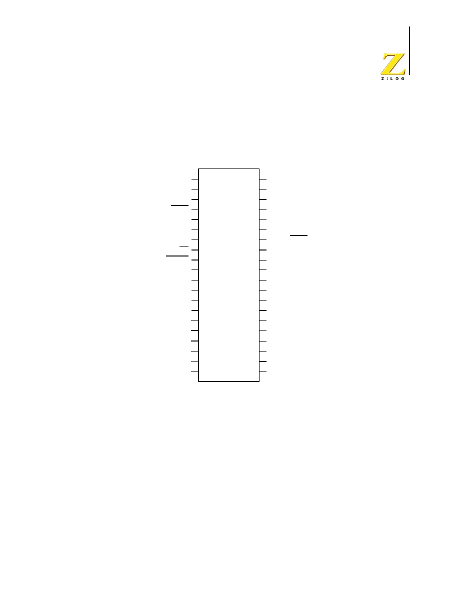
64K Series in 40-Pin Dual Inline Package (PDIP) . . . . . . . . . . . . . . . . . . . . 7
Figure 3.
64K Series in 44-Pin Plastic Leaded Chip Carrier (PLCC) . . . . . . . . . . . . . . 8
Figure 4.
64K Series in 44-Pin Low-Profile Quad Flat Package (LQFP) . . . . . . . . . . . 9
Figure 5.
64K Series in 64-Pin Low-Profile Quad Flat Package (LQFP) . . . . . . . . . . 10
Figure 6.
64K Series in 68-Pin Plastic Leaded Chip Carrier (PLCC) . . . . . . . . . . . . . 11
Figure 7.
64K Series in 80-Pin Quad Flat Package (QFP) . . . . . . . . . . . . . . . . . . . . . 12
Figure 8.
Power-On Reset Operation) . . . . . . . . . . . . . . . . . . . . . . . . . . . . . . . . . . . . . 45
Figure 9.
Voltage Brown-Out Reset Operation . . . . . . . . . . . . . . . . . . . . . . . . . . . . . . 46
Figure 10. GPIO Port Pin Block Diagram . . . . . . . . . . . . . . . . . . . . . . . . . . . . . . . . . . . 52
Figure 11. Interrupt Controller Block Diagram . . . . . . . . . . . . . . . . . . . . . . . . . . . . . . 64
Figure 12. Timer Block Diagram . . . . . . . . . . . . . . . . . . . . . . . . . . . . . . . . . . . . . . . . . 76
Figure 13. UART Block Diagram . . . . . . . . . . . . . . . . . . . . . . . . . . . . . . . . . . . . . . . . . 99
Figure 14. UART Asynchronous Data Format without Parity . . . . . . . . . . . . . . . . . . 100
Figure 15. UART Asynchronous Data Format with Parity . . . . . . . . . . . . . . . . . . . . . 100
Figure 16. UART Asynchronous MULTIPROCESSOR Mode Data Format . . . . . . 104
Figure 17. UART Driver Enable Signal Timing
(shown with 1 Stop Bit and Parity) . . . . . . . . . . . . . . . . . . . . . . . . . . . . . . 106
Figure 18. UART Receiver Interrupt Service Routine Flow . . . . . . . . . . . . . . . . . . . 108
Figure 19. Infrared Data Communication System Block Diagram . . . . . . . . . . . . . . . 120
Figure 20. Infrared Data Transmission . . . . . . . . . . . . . . . . . . . . . . . . . . . . . . . . . . . . 122
Figure 21. Infrared Data Reception . . . . . . . . . . . . . . . . . . . . . . . . . . . . . . . . . . . . . . . 123
Figure 22. SPI Configured as a Master in a Single Master, Single Slave System . . . 125
Figure 23. SPI Configured as a Master in a Single Master, Multiple Slave System . . 126
Figure 24. SPI Configured as a Slave . . . . . . . . . . . . . . . . . . . . . . . . . . . . . . . . . . . . . 126
Figure 25. SPI Timing When PHASE is 0 . . . . . . . . . . . . . . . . . . . . . . . . . . . . . . . . . 129
Figure 26. SPI Timing When PHASE is 1 . . . . . . . . . . . . . . . . . . . . . . . . . . . . . . . . . 130
Figure 27. I2C Controller Block Diagram . . . . . . . . . . . . . . . . . . . . . . . . . . . . . . . . . 140
Figure 28. 7-Bit Address Only Transaction Format . . . . . . . . . . . . . . . . . . . . . . . . . . 144
Figure 29. 7-Bit Addressed Slave Data Transfer Format . . . . . . . . . . . . . . . . . . . . . . 145
Figure 30. 10-Bit Address Only Transaction Format . . . . . . . . . . . . . . . . . . . . . . . . . 146
Figure 31. 10-Bit Addressed Slave Data Transfer Format . . . . . . . . . . . . . . . . . . . . . 147
Figure 32. Receive Data Transfer Format for a 7-Bit Addressed Slave . . . . . . . . . . . 149

PS019915-1005
List
of
Figures
Z8 Encore!
�
64K Series
Product Specification
xii
Figure 33. Receive Data Format for a 10-Bit Addressed Slave . . . . . . . . . . . . . . . . . 150
Figure 34. Analog-to-Digital Converter Block Diagram . . . . . . . . . . . . . . . . . . . . . . 172
Figure 35. Flash Memory Arrangement . . . . . . . . . . . . . . . . . . . . . . . . . . . . . . . . . . . 179
Figure 36. On-Chip Debugger Block Diagram . . . . . . . . . . . . . . . . . . . . . . . . . . . . . . 193
Figure 37. Interfacing the On-Chip Debugger's DBG Pin
with an RS-232 Interface (1) . . . . . . . . . . . . . . . . . . . . . . . . . . . . . . . . . . . 194
Figure 38. Interfacing the On-Chip Debugger's DBG Pin
with an RS-232 Interface (2) . . . . . . . . . . . . . . . . . . . . . . . . . . . . . . . . . . . 195
Figure 39. OCD Data Format 196
Figure 40. Recommended 20MHz Crystal Oscillator Configuration . . . . . . . . . . . . . 206
Figure 41. Connecting the On-Chip Oscillator to an External RC Network . . . . . . . . 207
Figure 42. Typical RC Oscillator Frequency as a Function of the
External Capacitance with a 45kW Resistor . . . . . . . . . . . . . . . . . . . . . . . 208
Figure 43. Typical Active Mode Idd Versus System Clock Frequency . . . . . . . . . . . 213
Figure 44. Maximum Active Mode Idd Versus System Clock Frequency . . . . . . . . . 214
Figure 45. Typical HALT Mode Idd Versus System Clock Frequency . . . . . . . . . . . 215
Figure 46. Maximum HALT Mode Icc Versus System Clock Frequency . . . . . . . . . 216
Figure 47. Maximum STOP Mode Idd with VBO enabled
versus Power Supply Voltage . . . . . . . . . . . . . . . . . . . . . . . . . . . . . . . . . . 217
Figure 48. Maximum STOP Mode Idd with VBO Disabled
versus Power Supply Voltage . . . . . . . . . . . . . . . . . . . . . . . . . . . . . . . . . . 218
Figure 49. Analog-to-Digital Converter Frequency Response . . . . . . . . . . . . . . . . . . 223
Figure 50. Port Input Sample Timing . . . . . . . . . . . . . . . . . . . . . . . . . . . . . . . . . . . . . 225
Figure 51. GPIO Port Output Timing . . . . . . . . . . . . . . . . . . . . . . . . . . . . . . . . . . . . . 226
Figure 52. On-Chip Debugger Timing . . . . . . . . . . . . . . . . . . . . . . . . . . . . . . . . . . . . 227
Figure 53. SPI Master Mode Timing . . . . . . . . . . . . . . . . . . . . . . . . . . . . . . . . . . . . . 228
Figure 54. SPI Slave Mode Timing . . . . . . . . . . . . . . . . . . . . . . . . . . . . . . . . . . . . . . . 229
Figure 55. I2C Timing . . . . . . . . . . . . . . . . . . . . . . . . . . . . . . . . . . . . . . . . . . . . . . . . . 230
Figure 56. UART Timing with CTS . . . . . . . . . . . . . . . . . . . . . . . . . . . . . . . . . . . . . . 231
Figure 57. UART Timing without CTS . . . . . . . . . . . . . . . . . . . . . . . . . . . . . . . . . . . 232
Figure 58. Flags Register . . . . . . . . . . . . . . . . . . . . . . . . . . . . . . . . . . . . . . . . . . . . . . 252
Figure 59. Opcode Map Cell Description . . . . . . . . . . . . . . . . . . . . . . . . . . . . . . . . . . 253
Figure 60. First Opcode Map . . . . . . . . . . . . . . . . . . . . . . . . . . . . . . . . . . . . . . . . . . . 255
Figure 61. Second Opcode Map after 1FH . . . . . . . . . . . . . . . . . . . . . . . . . . . . . . . . . 256
Figure 62. 40-Lead Plastic Dual-Inline Package (PDIP) . . . . . . . . . . . . . . . . . . . . . . 257
Figure 63. 44-Lead Low-Profile Quad Flat Package (LQFP) . . . . . . . . . . . . . . . . . . . 258
Figure 64. 44-Lead Plastic Lead Chip Carrier Package (PLCC) . . . . . . . . . . . . . . . . 259

PS019915-1005
List
of
Figures
Z8 Encore!
�
64K Series
Product Specification
xiii
Figure 65. 64-Lead Low-Profile Quad Flat Package (LQFP) . . . . . . . . . . . . . . . . . . . 259
Figure 66. 68-Lead Plastic Lead Chip Carrier Package (PLCC) . . . . . . . . . . . . . . . . 260
Figure 67. 80-Lead Quad-Flat Package (QFP) . . . . . . . . . . . . . . . . . . . . . . . . . . . . . . 261

PS019915-1005
List of Tables
Z8 Encore!
�
64K Series
Product Specification
xiv
List of Tables
Table 1.
Revision History of this Document . . . . . . . . . . . . . . . . . . . . . . . . . . . . . . . .iii
Table 2.
Z8 Encore!� 64K Series Part Selection Guide . . . . . . . . . . . . . . . . . . . . . . . 2
Table 3.
Z8 Encore!� 64K Series Package Options . . . . . . . . . . . . . . . . . . . . . . . . . . 6
Table 4.
Signal Descriptions . . . . . . . . . . . . . . . . . . . . . . . . . . . . . . . . . . . . . . . . . . . 13
Table 5.
Pin Characteristics of the 64K Series . . . . . . . . . . . . . . . . . . . . . . . . . . . . . 16
Table 6.
Z8 Encore� 64K Series Program Memory Maps . . . . . . . . . . . . . . . . . . . . 18
Table 7.
Z8 Encore!� 64K Series Information Area Map . . . . . . . . . . . . . . . . . . . . 20
Table 8.
64K Series Register File Address Map . . . . . . . . . . . . . . . . . . . . . . . . . . . . 21
Table 9.
Reset and STOP Mode Recovery Characteristics and Latency . . . . . . . . . . 43
Table 10.
Reset Sources and Resulting Reset Type . . . . . . . . . . . . . . . . . . . . . . . . . . . 44
Table 11.
STOP Mode Recovery Sources and Resulting Action . . . . . . . . . . . . . . . . 47
Table 12.
Port Availability by Device and Package Type . . . . . . . . . . . . . . . . . . . . . . 51
Table 13.
Port Alternate Function Mapping . . . . . . . . . . . . . . . . . . . . . . . . . . . . . . . . 53
Table 14.
Port A-H GPIO Address Registers (PxADDR) . . . . . . . . . . . . . . . . . . . . . . 55
Table 15.
GPIO Port Registers and Sub-Registers . . . . . . . . . . . . . . . . . . . . . . . . . . . 55
Table 16.
Port A�H Control Registers (PxCTL) . . . . . . . . . . . . . . . . . . . . . . . . . . . . . 56
Table 17.
Port A-H Data Direction Sub-Registers . . . . . . . . . . . . . . . . . . . . . . . . . . . . 57
Table 18.
Port A-H Alternate Function Sub-Registers . . . . . . . . . . . . . . . . . . . . . . . . 57
Table 19.
Port A-H Output Control Sub-Registers . . . . . . . . . . . . . . . . . . . . . . . . . . . 58
Table 20.
Port A�H High Drive Enable Sub-Registers . . . . . . . . . . . . . . . . . . . . . . . . 59
Table 21.
Port A�H Input Data Registers (PxIN) . . . . . . . . . . . . . . . . . . . . . . . . . . . . 60
Table 22.
Port A-H STOP Mode Recovery Source Enable Sub-Registers . . . . . . . . . 60
Table 23.
Port A-H Output Data Register (PxOUT) . . . . . . . . . . . . . . . . . . . . . . . . . . 61
Table 24.
Interrupt Vectors in Order of Priority . . . . . . . . . . . . . . . . . . . . . . . . . . . . . 63
Table 25.
Interrupt Request 0 Register (IRQ0) . . . . . . . . . . . . . . . . . . . . . . . . . . . . . . 66
Table 26.
Interrupt Request 1 Register (IRQ1) . . . . . . . . . . . . . . . . . . . . . . . . . . . . . . 68
Table 27.
Interrupt Request 2 Register (IRQ2) . . . . . . . . . . . . . . . . . . . . . . . . . . . . . . 68
Table 28.
IRQ0 Enable and Priority Encoding . . . . . . . . . . . . . . . . . . . . . . . . . . . . . . 69
Table 29.
IRQ0 Enable High Bit Register (IRQ0ENH) . . . . . . . . . . . . . . . . . . . . . . . 69
Table 30.
IRQ0 Enable Low Bit Register (IRQ0ENL) . . . . . . . . . . . . . . . . . . . . . . . . 70
Table 31.
IRQ1 Enable and Priority Encoding . . . . . . . . . . . . . . . . . . . . . . . . . . . . . . 70
Table 32.
IRQ1 Enable Low Bit Register (IRQ1ENL) . . . . . . . . . . . . . . . . . . . . . . . . 71
Table 33.
IRQ2 Enable and Priority Encoding . . . . . . . . . . . . . . . . . . . . . . . . . . . . . . 71

PS019915-1005
List of Tables
Z8 Encore!
�
64K Series
Product Specification
xv
Table 34.
IRQ1 Enable High Bit Register (IRQ1ENH) . . . . . . . . . . . . . . . . . . . . . . . 71
Table 35.
IRQ2 Enable Low Bit Register (IRQ2ENL) . . . . . . . . . . . . . . . . . . . . . . . . 72
Table 36.
IRQ2 Enable High Bit Register (IRQ2ENH) . . . . . . . . . . . . . . . . . . . . . . . 72
Table 37.
Interrupt Edge Select Register (IRQES) . . . . . . . . . . . . . . . . . . . . . . . . . . . 73
Table 38.
Interrupt Port Select Register (IRQPS) . . . . . . . . . . . . . . . . . . . . . . . . . . . . 73
Table 39.
Interrupt Control Register (IRQCTL) . . . . . . . . . . . . . . . . . . . . . . . . . . . . . 74
Table 40.
Timer 0-3 High Byte Register (TxH) . . . . . . . . . . . . . . . . . . . . . . . . . . . . . 85
Table 41.
Timer 0-3 Low Byte Register (TxL) . . . . . . . . . . . . . . . . . . . . . . . . . . . . . . 85
Table 42.
Timer 0-3 Reload High Byte Register (TxRH) . . . . . . . . . . . . . . . . . . . . . . 86
Table 43.
Timer 0-3 Reload Low Byte Register (TxRL) . . . . . . . . . . . . . . . . . . . . . . . 86
Table 44.
Timer 0-3 PWM High Byte Register (TxPWMH) . . . . . . . . . . . . . . . . . . . 87
Table 45.
Timer 0-3 PWM Low Byte Register (TxPWML) . . . . . . . . . . . . . . . . . . . . 87
Table 46.
Timer 0-3 Control 0 Register (TxCTL0) . . . . . . . . . . . . . . . . . . . . . . . . . . . 88
Table 47.
Timer 0-3 Control 1 Register (TxCTL1) . . . . . . . . . . . . . . . . . . . . . . . . . . . 88
Table 48.
Watch-Dog Timer Approximate Time-Out Delays . . . . . . . . . . . . . . . . . . . 92
Table 49.
Watch-Dog Timer Control Register (WDTCTL) . . . . . . . . . . . . . . . . . . . . 94
Table 50.
Watch-Dog Timer Reload Upper Byte Register (WDTU) . . . . . . . . . . . . . 96
Table 51.
Watch-Dog Timer Reload High Byte Register (WDTH) . . . . . . . . . . . . . . 96
Table 52.
Watch-Dog Timer Reload Low Byte Register (WDTL) . . . . . . . . . . . . . . . 97
Table 53.
UART Transmit Data Register (UxTXD) . . . . . . . . . . . . . . . . . . . . . . . . . 109
Table 54.
UART Receive Data Register (UxRXD) . . . . . . . . . . . . . . . . . . . . . . . . . . 110
Table 55.
UART Status 0 Register (UxSTAT0) . . . . . . . . . . . . . . . . . . . . . . . . . . . . 110
Table 56.
UART Status 1 Register (UxSTAT1) . . . . . . . . . . . . . . . . . . . . . . . . . . . . 112
Table 57.
UART Control 0 Register (UxCTL0) . . . . . . . . . . . . . . . . . . . . . . . . . . . . 112
Table 58.
UART Control 1 Register (UxCTL1) . . . . . . . . . . . . . . . . . . . . . . . . . . . . 113
Table 59.
UART Address Compare Register (UxADDR) . . . . . . . . . . . . . . . . . . . . . 115
Table 60.
UART Baud Rate High Byte Register (UxBRH) . . . . . . . . . . . . . . . . . . . 116
Table 61.
UART Baud Rate Low Byte Register (UxBRL) . . . . . . . . . . . . . . . . . . . . 116
Table 62.
UART Baud Rates . . . . . . . . . . . . . . . . . . . . . . . . . . . . . . . . . . . . . . . . . . . 117
Table 63.
SPI Clock Phase (PHASE) and Clock Polarity (CLKPOL) Operation . . . 128
Table 64.
SPI Data Register (SPIDATA) . . . . . . . . . . . . . . . . . . . . . . . . . . . . . . . . . 133
Table 65.
SPI Control Register (SPICTL) . . . . . . . . . . . . . . . . . . . . . . . . . . . . . . . . . 134
Table 66.
SPI Status Register (SPISTAT) . . . . . . . . . . . . . . . . . . . . . . . . . . . . . . . . . 135
Table 67.
SPI Mode Register (SPIMODE) . . . . . . . . . . . . . . . . . . . . . . . . . . . . . . . . 136
Table 68.
SPI Diagnostic State Register (SPIDST) . . . . . . . . . . . . . . . . . . . . . . . . . . 137
Table 69.
SPI Baud Rate High Byte Register (SPIBRH) . . . . . . . . . . . . . . . . . . . . . 138

PS019915-1005
List of Tables
Z8 Encore!
�
64K Series
Product Specification
xvi
Table 70.
SPI Baud Rate Low Byte Register (SPIBRL) . . . . . . . . . . . . . . . . . . . . . . 138
Table 71.
I2C Data Register (I2CDATA) . . . . . . . . . . . . . . . . . . . . . . . . . . . . . . . . . 153
Table 72.
I2C Status Register (I2CSTAT) . . . . . . . . . . . . . . . . . . . . . . . . . . . . . . . . . 153
Table 73.
I2C Control Register (I2CCTL) . . . . . . . . . . . . . . . . . . . . . . . . . . . . . . . . . 155
Table 74.
I2C Baud Rate High Byte Register (I2CBRH) . . . . . . . . . . . . . . . . . . . . . 157
Table 75.
I2C Baud Rate Low Byte Register (I2CBRL) . . . . . . . . . . . . . . . . . . . . . . 157
Table 76.
I2C Diagnostic State Register (I2CDST) . . . . . . . . . . . . . . . . . . . . . . . . . . 158
Table 77.
I2C Diagnostic Control Register (I2CDIAG) . . . . . . . . . . . . . . . . . . . . . . 160
Table 78.
DMAx Control Register (DMAxCTL) . . . . . . . . . . . . . . . . . . . . . . . . . . . 164
Table 79.
DMAx I/O Address Register (DMAxIO) . . . . . . . . . . . . . . . . . . . . . . . . . 165
Table 80.
DMAx Address High Nibble Register (DMAxH) . . . . . . . . . . . . . . . . . . . 165
Table 81.
DMAx Start/Current Address Low Byte Register (DMAxSTART) . . . . . 166
Table 82.
DMAx End Address Low Byte Register (DMAxEND) . . . . . . . . . . . . . . 167
Table 83.
DMA_ADC Register File Address Example . . . . . . . . . . . . . . . . . . . . . . . 167
Table 84.
DMA_ADC Address Register (DMAA_ADDR) . . . . . . . . . . . . . . . . . . . 168
Table 85.
DMA_ADC Control Register (DMAACTL) . . . . . . . . . . . . . . . . . . . . . . . 169
Table 86.
DMA_ADC Status Register (DMAA_STAT) . . . . . . . . . . . . . . . . . . . . . . 170
Table 87.
ADC Control Register (ADCCTL) . . . . . . . . . . . . . . . . . . . . . . . . . . . . . . 175
Table 88.
ADC Data High Byte Register (ADCD_H) . . . . . . . . . . . . . . . . . . . . . . . . 176
Table 89.
ADC Data Low Bits Register (ADCD_L) . . . . . . . . . . . . . . . . . . . . . . . . . 177
Table 90.
Flash Memory Configurations . . . . . . . . . . . . . . . . . . . . . . . . . . . . . . . . . . 178
Table 91.
Flash Memory Sector Addresses . . . . . . . . . . . . . . . . . . . . . . . . . . . . . . . . 179
Table 92.
64K Series Information Area Map . . . . . . . . . . . . . . . . . . . . . . . . . . . . . . . 180
Table 93.
Flash Control Register (FCTL) . . . . . . . . . . . . . . . . . . . . . . . . . . . . . . . . . 185
Table 94.
Flash Status Register (FSTAT) . . . . . . . . . . . . . . . . . . . . . . . . . . . . . . . . . 186
Table 95.
Page Select Register (FPS) . . . . . . . . . . . . . . . . . . . . . . . . . . . . . . . . . . . . 187
Table 96.
Flash Sector Protect Register (FPROT) . . . . . . . . . . . . . . . . . . . . . . . . . . . 188
Table 97.
Flash Frequency High Byte Register (FFREQH) . . . . . . . . . . . . . . . . . . . 189
Table 98.
Flash Frequency Low Byte Register (FFREQL) . . . . . . . . . . . . . . . . . . . . 189
Table 99.
Flash Option Bits At Flash Memory Address 0000H . . . . . . . . . . . . . . . . 191
Table 100. Options Bits at Flash Memory Address 0001H . . . . . . . . . . . . . . . . . . . . . 192
Table 101. OCD Baud-Rate Limits . . . . . . . . . . . . . . . . . . . . . . . . . . . . . . . . . . . . . . . 196
Table 102. On-Chip Debugger Commands . . . . . . . . . . . . . . . . . . . . . . . . . . . . . . . . . 198
Table 103. OCD Control Register (OCDCTL) . . . . . . . . . . . . . . . . . . . . . . . . . . . . . . 203
Table 104. OCD Status Register (OCDSTAT) . . . . . . . . . . . . . . . . . . . . . . . . . . . . . . 204
Table 105. Recommended Crystal Oscillator Specifications (20MHz Operation) . . . 206

PS019915-1005
List of Tables
Z8 Encore!
�
64K Series
Product Specification
xvii
Table 106. Absolute Maximum Ratings . . . . . . . . . . . . . . . . . . . . . . . . . . . . . . . . . . . 209
Table 107. DC Characteristics . . . . . . . . . . . . . . . . . . . . . . . . . . . . . . . . . . . . . . . . . . . 211
Table 108. Power-On Reset and Voltage Brown-Out Electrical
Characteristics and Timing . . . . . . . . . . . . . . . . . . . . . . . . . . . . . . . . . . . . 219
Table 109. Reset and STOP Mode Recovery Pin Timing . . . . . . . . . . . . . . . . . . . . . . 220
Table 110. External RC Oscillator Electrical Characteristics and Timing . . . . . . . . . 220
Table 111. Flash Memory Electrical Characteristics and Timing . . . . . . . . . . . . . . . . 221
Table 112. Watch-Dog Timer Electrical Characteristics and Timing . . . . . . . . . . . . . 221
Table 113. Analog-to-Digital Converter Electrical Characteristics and Timing . . . . . 222
Table 114. AC Characteristics . . . . . . . . . . . . . . . . . . . . . . . . . . . . . . . . . . . . . . . . . . . 224
Table 115. GPIO Port Input Timing . . . . . . . . . . . . . . . . . . . . . . . . . . . . . . . . . . . . . . 225
Table 116. GPIO Port Output Timing . . . . . . . . . . . . . . . . . . . . . . . . . . . . . . . . . . . . . 226
Table 117. On-Chip Debugger Timing . . . . . . . . . . . . . . . . . . . . . . . . . . . . . . . . . . . . 227
Table 118. SPI Master Mode Timing . . . . . . . . . . . . . . . . . . . . . . . . . . . . . . . . . . . . . 228
Table 119. SPI Slave Mode Timing . . . . . . . . . . . . . . . . . . . . . . . . . . . . . . . . . . . . . . . 229
Table 120. I2C Timing . . . . . . . . . . . . . . . . . . . . . . . . . . . . . . . . . . . . . . . . . . . . . . . . . 230
Table 121. UART Timing with CTS . . . . . . . . . . . . . . . . . . . . . . . . . . . . . . . . . . . . . . 231
Table 122. UART Timing without CTS . . . . . . . . . . . . . . . . . . . . . . . . . . . . . . . . . . . 232
Table 123. Notational Shorthand . . . . . . . . . . . . . . . . . . . . . . . . . . . . . . . . . . . . . . . . . 235
Table 124. Additional Symbols . . . . . . . . . . . . . . . . . . . . . . . . . . . . . . . . . . . . . . . . . . 236
Table 125. Condition Codes . . . . . . . . . . . . . . . . . . . . . . . . . . . . . . . . . . . . . . . . . . . . 237
Table 126. Arithmetic Instructions . . . . . . . . . . . . . . . . . . . . . . . . . . . . . . . . . . . . . . . 238
Table 127. Bit Manipulation Instructions . . . . . . . . . . . . . . . . . . . . . . . . . . . . . . . . . . 239
Table 128. Block Transfer Instructions . . . . . . . . . . . . . . . . . . . . . . . . . . . . . . . . . . . . 239
Table 129. CPU Control Instructions . . . . . . . . . . . . . . . . . . . . . . . . . . . . . . . . . . . . . . 240
Table 130. Load Instructions . . . . . . . . . . . . . . . . . . . . . . . . . . . . . . . . . . . . . . . . . . . . 240
Table 131. Logical Instructions . . . . . . . . . . . . . . . . . . . . . . . . . . . . . . . . . . . . . . . . . . 241
Table 132. Program Control Instructions . . . . . . . . . . . . . . . . . . . . . . . . . . . . . . . . . . . 241
Table 133. Rotate and Shift Instructions . . . . . . . . . . . . . . . . . . . . . . . . . . . . . . . . . . . 242
Table 134. eZ8 CPU Instruction Summary . . . . . . . . . . . . . . . . . . . . . . . . . . . . . . . . . 242
Table 135. Opcode Map Abbreviations . . . . . . . . . . . . . . . . . . . . . . . . . . . . . . . . . . . . 254

Z8 Encore!
�
64K Series
Product Specification
PS019915-1005
Manual
Objectives
xviii
Manual Objectives
This Product Specification provides detailed operating information for the Flash devices
within the Z8 Encore!
�
64K Series Microcontroller (MCU) products. Within this docu-
ment, the Z8F642x, Z8F482x, Z8F322x, Z8F242x, and Z8F162x devices are referred to
collectively as the Z8 Encore!
�
64K Series unless specifically stated otherwise.
About This Manual
ZiLOG recommends that the user read and understand everything in this manual before
setting up and using the product. However, we recognize that there are different styles of
learning. Therefore, we have designed this Product Specification to be used either as a
how to procedural manual or a reference guide to important data.
Intended Audience
This document is written for ZiLOG customers who are experienced at working with
microcontrollers, integrated circuits, or printed circuit assemblies.
Manual Conventions
The following assumptions and conventions are adopted to provide clarity and ease of use:
Courier Typeface
Commands, code lines and fragments, bits, equations, hexadecimal addresses, and various
executable items are distinguished from general text by the use of the
Courier
typeface.
Where the use of the font is not indicated, as in the Index, the name of the entity is pre-
sented in upper case.
�
Example: FLAGS[1] is
smrf
.
Hexadecimal Values
Hexadecimal values are designated by uppercase H suffix and appear in the
Courier
typeface.
�
Example: R1 is set to
F8H.
Brackets
The square brackets, [ ], indicate a register or bus.

PS019915-1005
Manual
Objectives
Z8 Encore!
�
64K Series
Product Specification
xix
�
Example: for the register R1[7:0], R1 is an 8-bit register, R1[7] is the most significant
bit, and R1[0] is the least significant bit.
Braces
The curly braces, { }, indicate a single register or bus created by concatenating some com-
bination of smaller registers, buses, or individual bits.
�
Example: the 12-bit register address {
0H
, RP[7:4], R1[3:0]} is composed of a 4-bit
hexadecimal value (
0H
) and two 4-bit register values taken from the Register Pointer
(RP) and Working Register R1.
0H
is the most significant nibble (4-bit value) of the
12-bit register, and R1[3:0] is the least significant nibble of the 12-bit register.
Parentheses
The parentheses, ( ), indicate an indirect register address lookup.
�
Example: (R1) is the memory location referenced by the address contained in the
Working Register R1.
Parentheses/Bracket Combinations
The parentheses, ( ), indicate an indirect register address lookup and the square brackets,
[ ], indicate a register or bus.
�
Example: assume PC[15:0] contains the value
1234h
. (PC[15:0]) then refers to the
contents of the memory location at address
1234h
.
Use of the Words Set, Reset and Clear
The word set implies that a register bit or a condition contains a logical 1. The words reset
or clear imply that a register bit or a condition contains a logical 0. When either of these
terms is followed by a number, the word logical may not be included; however, it is
implied.
Notation for Bits and Similar Registers
A field of bits within a register is designated as: Register[n:n].
�
Example: ADDR[15:0] refers to bits 15 through bit 0 of the Address.
Use of the Terms LSB, MSB, lsb, and msb
In this document, the terms LSB and MSB, when appearing in upper case, mean least sig-
nificant byte and most significant byte, respectively. The lowercase forms, lsb and msb,
mean least significant bit and most significant bit, respectively.
Use of Initial Uppercase Letters
Initial uppercase letters designate settings and conditions in general text.
�
Example 1: The receiver forces the SCL line to Low.

PS019915-1005
Manual
Objectives
Z8 Encore!
�
64K Series
Product Specification
xx
�
Example 2: The Master can generate a Stop condition to abort the transfer.
Use of All Uppercase Letters
The use of all uppercase letters designates the names of states, modes, and commands.
�
Example 1: The bus is considered BUSY after the Start condition.
�
Example 2: A START command triggers the processing of the initialization sequence.
�
Example 3: STOP mode
Bit Numbering
Bits are numbered from 0 to n�1 where n indicates the total number of bits. For example,
the 8 bits of a register are numbered from 0 to 7.
Safeguards
It is important that all users understand the following safety terms, which are defined here.
Indicates a procedure or file may become corrupted if the user does not fol-
low directions.
Trademarks
ZiLOG
�
, eZ8, Z8 Encore!
�
, and Z8
�
are trademarks of
ZiLOG, Inc.
in the U.S.A. and
other countries. All other trademarks are the property of their respective corporations.
Caution:

Z8 Encore!
�
64K Series
Product Specification
PS019915-1005
Introduction
1
Introduction
The Z8 Encore!
�
MCU family of products are a line of ZiLOG microcontroller products
based upon the 8-bit eZ8 CPU. The Z8 Encore!
�
64K Series, hereafter referred to collec-
tively as the Z8 Encore!
�
or the 64K Series adds Flash memory to ZiLOG's extensive line
of 8-bit microcontrollers. The Flash in-circuit programming capability allows for faster
development time and program changes in the field. The new eZ8 CPU is upward compat-
ible with existing Z8
�
instructions. The rich peripheral set of the Z8 Encore!
�
makes it
suitable for a variety of applications including motor control, security systems, home
appliances, personal electronic devices, and sensors.
Features
�
20 MHz eZ8 CPU
�
Up to 64 KB Flash with in-circuit programming capability
�
Up to 4 KB register RAM
�
12-channel, 10-bit analog-to-digital converter (ADC)
�
Two full-duplex 9-bit UARTs with bus transceiver Driver Enable control
�
I
2
C
�
Serial Peripheral Interface
�
Two Infrared Data Association (IrDA)-compliant infrared encoder/decoder
s
�
Up to four 16-bit timers with capture, compare, and PWM capability
�
Watch-Dog Timer (WDT) with internal RC oscillator
�
3-channel DMA
�
Up to 60 I/O pins
�
24 interrupts with configurable priority
�
On-Chip Debugger
�
Voltage Brown-out Protection (VBO)
�
Power-On Reset (POR)

PS019915-1005
Introduction
Z8 Encore!
�
64K Series
Product Specification
2
�
3.0-3.6V operating voltage with 5V-tolerant inputs
�
0� to +70�C, �40� to +105�C, and �40� to +125�C operating temperature ranges
Part Selection Guide
Table 1 identifies the basic features and package styles available for each device within the
Z8 Encore!
�
product line.
Table 1. Z8 Encore!
�
64K Series Part Selection Guide
Part
Number
Flash
(KB)
RAM
(KB) I/O
16-bit Timers
with PWM
ADC
Inputs
UARTs
with IrDA I
2
C SPI
40/44-pin
packages
64/68-pin
packages
80-pin
package
Z8F1621
16
2
31
3
8
2
1
1
X
Z8F1622
16
2
46
4
12
2
1
1
X
Z8F2421
24
2
31
3
8
2
1
1
X
Z8F2422
24
2
46
4
12
2
1
1
X
Z8F3221
32
2
31
3
8
2
1
1
X
Z8F3222
32
2
46
4
12
2
1
1
X
Z8F4821
48
4
31
3
8
2
1
1
X
Z8F4822
48
4
46
4
12
2
1
1
X
Z8F4823
48
4
60
4
12
2
1
1
X
Z8F6421
64
4
31
3
8
2
1
1
X
Z8F6422
64
4
46
4
12
2
1
1
X
Z8F6423
64
4
60
4
12
2
1
1
X
Die Form
Sales
Please
contact
ZiLOG
PS019915-1005
Introduction
Z8 Encore!
�
64K Series
Product Specification
3
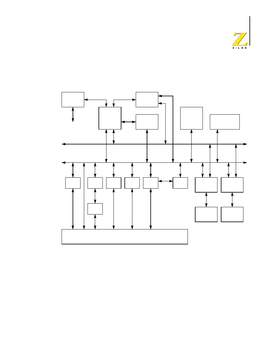
Block Diagram
Figure 1 illustrates the block diagram of the architecture of the Z8 Encore!
�
64K Series.
Figure 1. Z8 Encore!
�
64K Series Block Diagram
CPU and Peripheral Overview
eZ8 CPU Features
The eZ8, ZiLOG's latest 8-bit Central Processing Unit (CPU), meets the continuing
demand for faster and more code-efficient microcontrollers. The eZ8 CPU executes a
superset of the original Z8 instruction set. The eZ8 CPU features include:
�
Direct register-to-register architecture allows each register to function as an
accumulator, improving execution time and decreasing the required program memory
GPIO
IrDA
UARTs
I
2
C
Timers
SPI
ADC
Flash
Controller
RAM
RAM
Controller
Flash
Interrupt
Controller
On-Chip
Debugger
eZ8
CPU
WDT with
RC Oscillator
POR/VBO
& Reset
Controller
XTAL / RC
Oscillator
Register Bus
Memory Busses
System
Clock
DMA
Memory

PS019915-1005
Introduction
Z8 Encore!
�
64K Series
Product Specification
4
�
Software stack allows much greater depth in subroutine calls and interrupts than
hardware stacks
�
Compatible with existing Z8
�
code
�
Expanded internal Register File allows access of up to 4KB
�
New instructions improve execution efficiency for code developed using higher-level
programming languages, including C
�
Pipelined instruction fetch and execution
�
New instructions for improved performance including BIT, BSWAP, BTJ, CPC, LDC,
LDCI, LEA, MULT, and SRL
�
New instructions support 12-bit linear addressing of the Register File
�
Up to 10 MIPS operation
�
C-Compiler friendly
�
2-9 clock cycles per instruction
For more information regarding the eZ8 CPU, refer to the eZ8 CPU User Manual avail-
able for download at
www.zilog.com
.
General Purpose I/O
The 64K Series features seven 8-bit ports (Ports A-G) and one 4-bit port (Port H) for gen-
eral purpose I/O (GPIO). Each pin is individually programmable. All ports (except B and
H) support 5V-tolerant inputs.
Flash Controller
The Flash Controller programs and erases the Flash memory.
10-Bit Analog-to-Digital Converter
The Analog-to-Digital Converter (ADC) converts an analog input signal to a 10-bit binary
number. The ADC accepts inputs from up to 12 different analog input sources.
UARTs
Each UART is full-duplex and capable of handling asynchronous data transfers. The
UARTs support 8- and 9-bit data modes, selectable parity, and an efficient bus transceiver
Driver Enable signal for controlling a multi-transceiver bus, such as RS-485.

PS019915-1005
Introduction
Z8 Encore!
�
64K Series
Product Specification
5
I
2
C
The inter-integrated circuit (I
2
C
�
) controller makes the Z8 Encore!
�
compatible with the
I
2
C protocol. The I
2
C controller consists of two bidirectional bus lines, a serial data (SDA)
line and a serial clock (SCL) line.
Serial Peripheral Interface
The serial peripheral interface (SPI) allows the Z8 Encore!
�
to exchange data between
other peripheral devices such as EEPROMs, A/D converters and ISDN devices. The SPI is
a full-duplex, synchronous, character-oriented channel that supports a four-wire interface.
Timers
Up to four 16-bit reloadable timers can be used for timing/counting events or for motor
control operations. These timers provide a 16-bit programmable reload counter and oper-
ate in One-Shot, Continuous, Gated, Capture, Compare, Capture and Compare, and PWM
modes. Only 3 timers (Timers 0-2) are available in the 44-pin packages.
Interrupt Controller
The 64K Series products support up to 24 interrupts. These interrupts consist of 12 inter-
nal and 12 general-purpose I/O pins. The interrupts have 3 levels of programmable inter-
rupt priority.
Reset Controller
The Z8 Encore!
�
can be reset using the RESET pin, power-on reset, Watch-Dog Timer
(WDT), STOP mode exit, or Voltage Brown-Out (VBO) warning signal.
On-Chip Debugger
The Z8 Encore!
�
features an integrated On-Chip Debugger (OCD). The OCD provides a
rich set of debugging capabilities, such as reading and writing registers, programming the
Flash, setting breakpoints and executing code. A single-pin interface provides communi-
cation to the OCD.
DMA Controller
The 64K Series features three channels of DMA. Two of the channels are for register
RAM to and from I/O operations. The third channel automatically controls the transfer of
data from the ADC to the memory.

Z8 Encore!
�
64K Series
Product Specification
PS019915-1005
Signal and Pin Descriptions
6
Signal and Pin Descriptions
Overview
The
Z8 Encore!
�
64K Series products are available in a variety of packages styles and pin
configurations. This chapter describes the signals and available pin configurations for
each of the package styles. For information regarding the physical package specifications,
please refer to Packaging on page 257.
Available Packages
Table 2 identifies the package styles that are available for each device within the
Z8
Encore!
�
64K Series product line.
Table 2. Z8 Encore!
�
64K Series Package Options
Part Number
40-Pin
PDIP
44-pin
LQFP
44-pin
PLCC
64-pin
LQFP
68-pin
PLCC
80-pin
QFP
Z8F1621
X
X
X
Z8F1622
X
X
Z8F2421
X
X
X
Z8F2422
X
X
Z8F3221
X
X
X
Z8F3222
X
X
Z8F4821
X
X
X
Z8F4822
X
X
Z8F4823
X
Z8F6421
X
X
X
Z8F6422
X
X
Z8F6423
X
PS019915-1005
Signal and Pin Descriptions
Z8 Encore!
�
64K Series
Product Specification
7
Pin Configurations
Figures 2 through 7 illustrate the pin configurations for all of the packages available in the
64K Series. Refer to Table 3 for a description of the signals. Timer 3 is not available in the
40-pin and 44-pin packages.
Figure 2. 64K Series in 40-Pin Dual Inline Package (PDIP)
PD5 / TXD1
PC4 / MOSI
PA4 / RXD0
PA5 / TXD0
PA6 / SCL
PA7 / SDA
PD6 / CTS1
PC3 / SCK
VSS
PD4/RXD1
PD3 / DE1
PC5 / MISO
PA3 / CTS0
PA2/DE0
PA1 /T0OUT
PA0 / T0IN
PC2 / SS
1
40
VDD
RESET
PC6 / T2IN *
DBG
PC1 / T1OUT
VSS
PD1
PD0
PC0 / T1IN
XOUT
AVSS
XIN
VREF
AVDD
PB2 / ANA2
PB3 / ANA3
PB7 / ANA7
PB0 / ANA0
PB1 / ANA1
PB4 / ANA4
20
21
PB6 / ANA6
PB5 / ANA5
5
10
15
35
30
25
VDD
* T2OUT is not supported.
Note: Timer 3 is not supported.
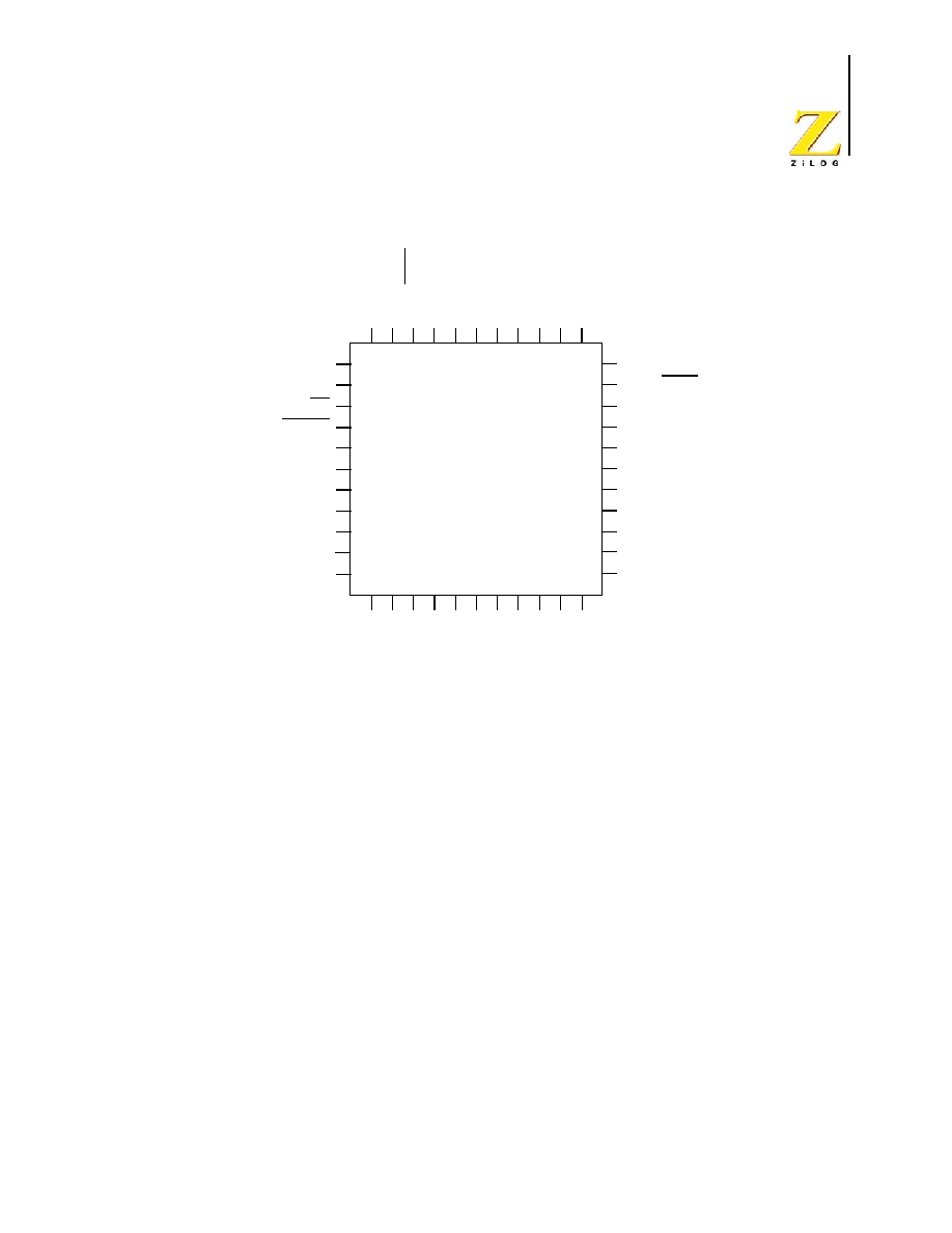
PS019915-1005
Signal and Pin Descriptions
Z8 Encore!
�
64K Series
Product Specification
8
Figure 3. 64K Series in 44-Pin Plastic Leaded Chip Carrier (PLCC)
PA7 / SDA
PD6 / CTS1
PC3 / SCK
VSS
VDD
VSS
PC7 / T2OUT
PC6 / T2IN
DBG
PA0 / T0IN
PD2
PC2 / SS
RESET
VDD
VSS
VDD
PD1
PD0
7
39
PC1 / T1OUT
XOUT
PC0 / T1IN
XIN
P
A
1 /
T
0
OUT
PA
2
/
DE
0
PA
3
/
CTS
0
PC5 / MISO
PD3 / DE1
PD4 / RXD1
PD5 / TX
D1
PC4 / MOSI
PA4
/
RXD0
PA5 / TXD0
PA6 / SCL
AVDD
PB6 / ANA6
PB5 / ANA5
PB0 / ANA0
PB1 / ANA1
PB4 / ANA4
PB7 / ANA7
VREF
PB2 / ANA2
PB3 /
ANA3
AVS
S
6
40
1
17
29
28
18
12
23
34
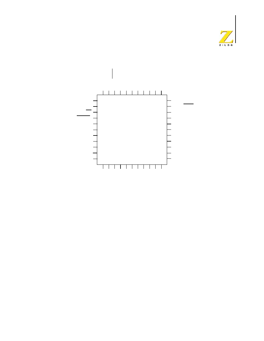
PS019915-1005
Signal and Pin Descriptions
Z8 Encore!
�
64K Series
Product Specification
9
Figure 4. 64K Series in 44-Pin Low-Profile Quad Flat Package (LQFP)
PA7 / SDA
PD6 / CTS1
PC3 / SCK
VSS
VDD
VSS
PC7 / T2OUT
PC6 / T2IN
DBG
PA0 / T0IN
PD2
PC2 / SS
RESET
VDD
VSS
VDD
PD1
PD0
34
22
PC1 / T1OUT
XOUT
PC0 / T1IN
XIN
P
A
1 /
T
0
OUT
PA
2
/
DE
0
PA
3
/
CTS
0
PC5 / MISO
PD3 / DE1
PD4 / RXD1
PD5 / TX
D1
PC4 / MOSI
PA4
/
RXD0
PA5 / TXD0
PA6 / SCL
AV
D
D
PB6 / ANA6
PB5 / ANA5
PB0 / ANA0
PB1 / ANA1
PB4 / ANA4
PB7 / ANA7
VREF
PB2 / ANA2
PB3 / ANA3
AVSS
33
23
44
12
11
1
28
39
17
6
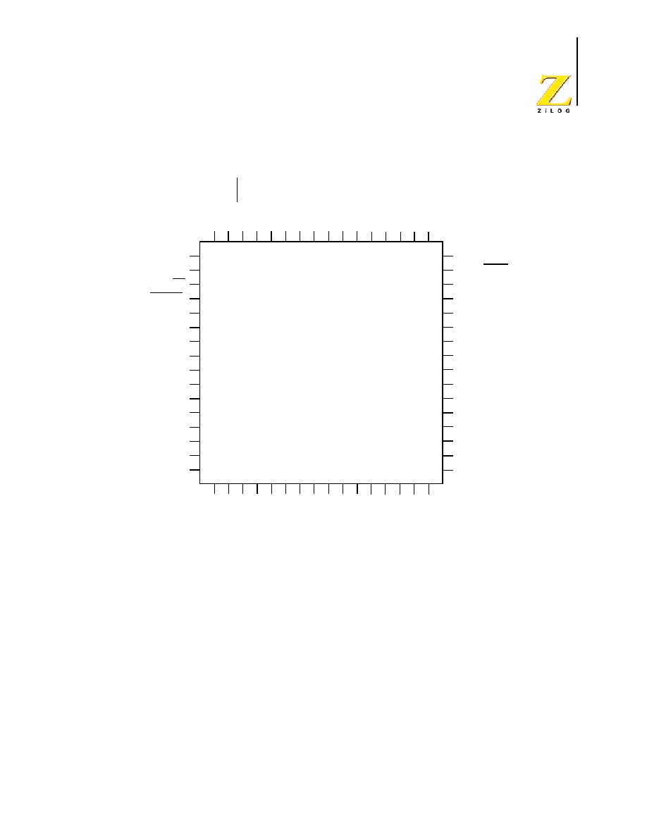
PS019915-1005
Signal and Pin Descriptions
Z8 Encore!
�
64K Series
Product Specification
10
Figure 5. 64K Series in 64-Pin Low-Profile Quad Flat Package (LQFP)
PA7 / SDA
PD6 / CTS1
PC3 / SCK
PD7 / RCOUT
VSS
PE5
PE6
PE7
VDD
PA0 / T0IN
PD2
PC2 / SS
RESET
VDD
PE4
PE3
VSS
PE2
49
32
PG3
PE1
VDD
PE0
PA1 / T0
OUT
PA2 / DE0
PA3 / CTS
0
VSS
VDD
PF7
PC5 /
MISO
PD4 / RXD1
PD5 / TXD1
PC4 / MOSI
VS
S
PB1 /
A
N
A1
PB0 /
A
N
A0
AVDD
PH0 /
A
N
A8
PH1 /
A
N
A9
PB4 /
A
N
A4
PB7 /
A
N
A7
PB6 /
A
N
A6
PB5 /
A
N
A5
PB3 /
A
N
A3
48
1
PC7 / T2OUT
PC6 / T2IN
DBG
PC1 / T1OUT
PC0 / T1IN
17
PB2 /
ANA2
VR
E
F
PH3 /
ANA11
PH2 /
ANA10
A
VSS
16
VSS
PD1 / T3OUT
PD0 / T3IN
XOUT
XIN
64
PD3 / DE1
VDD
PA4 / RXD0
PA5 / TXD0
PA6 / SCL
33
VSS
56
40
25
8
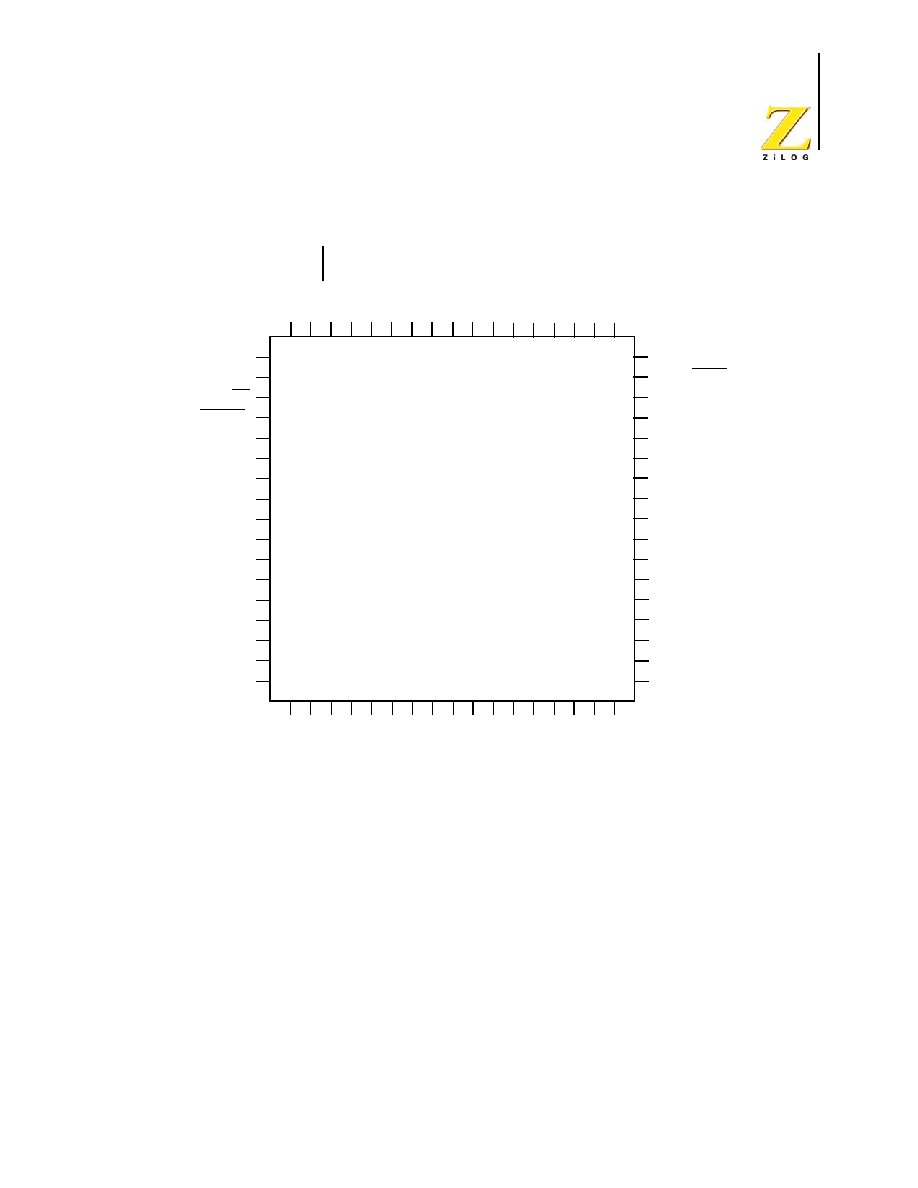
PS019915-1005
Signal and Pin Descriptions
Z8 Encore!
�
64K Series
Product Specification
11
Figure 6. 64K Series in 68-Pin Plastic Leaded Chip Carrier (PLCC)
PA7 / SDA
PD6 / CTS1
PC3 / SCK
PD7 / RCOUT
VSS
PE5
PE6
PE7
VDD
PA0 / T0IN
PD2
PC2 / SS
RESET
VDD
PE4
PE3
VSS
PE2
10
60
PG3
PE1
VDD
PE0
PA
1 /
T
0
OUT
PA
2 /
DE0
PA
3 /
CTS0
VS
S
VDD
PF7
PC5 /
M
I
SO
PD4 / RXD1
PD5 / TXD1
PC4 / MOSI
VS
S
PB1 /
A
N
A1
PB0 /
A
N
A0
AVDD
PH0 /
A
N
A8
PB4 /
A
N
A4
PB7 /
A
N
A7
PB6 /
A
N
A6
PB5 /
A
N
A5
PB3 /
A
N
A3
9
27
PC7 / T2OUT
PC6 / T2IN
DBG
PC1 / T1OUT
PC0 / T1IN
PB2 / ANA2
VR
E
F
PH3 /
ANA11
PH2 /
ANA10
A
VSS
VSS
VDD
PD1 / T3OUT
PD0 / T3IN
XOUT
PD3 / DE1
VS
S
PA4
/
RXD0
PA
5 /
TXD0
VDD
PH1 /
A
N
A9
PA6 / SCL
61
VSS
44
AVSS
43
XIN
26
1
VDD
18
35
52
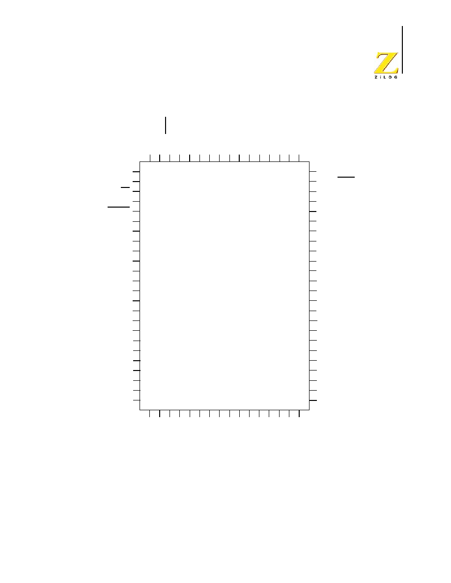
PS019915-1005
Signal and Pin Descriptions
Z8 Encore!
�
64K Series
Product Specification
12
Figure 7. 64K Series in 80-Pin Quad Flat Package (QFP)
PA7 / SDA
PD6 / CTS1
PC3 / SCK
PD7 / RCOUT
PG0
VSS
PG1
PG2
PE5
PA0 / T0IN
PD2
PC2 / SS
PF6
RESET
VDD
PF5
PF4
PF3
1
64
PE6
PE4
PE7
PE3
PA1 / T0
OUT
PA2 / DE0
PA3 / CTS0
VSS
VDD
PF7
PC
5 / M
I
S
O
PD4 /
RXD1
PD5 /
TXD1
PC4 /
MOS
I
VSS
PB1 / ANA
1
PB0 / ANA
0
AV
DD
PH0 / ANA
8
PB4 / ANA
4
PB7 / ANA
7
PB6 / ANA
6
PB5 / ANA
5
PB3 / ANA
3
80
25
VDD
PG3
PG4
PG5
PG6
PB2 / ANA2
VREF
PH3 /
ANA11
PH2 /
ANA10
AVSS
VSS
PE2
PE1
PE0
VSS
PD3 /
DE1
VDD
PA4 / RXD0
PA5 / TXD0
PA6 / SCL
VSS
PH1 / ANA
9
65
VDD
40
PF2
PG7
PF1
PC7 / T2OUT
PC6 / T2IN
DBG
PC1 / T1OUT
PC0 / T1IN
PF0
VDD
PD1 / T3OUT
PD0 / T3IN
XOUT
VSS
41
XIN
24
5
10
15
20
30
35
45
50
55
60
70
75

PS019915-1005
Signal and Pin Descriptions
Z8 Encore!
�
64K Series
Product Specification
13
Signal Descriptions
Table 3 describes the Z8 Encore! signals. Refer to the section Pin Configurations on
page 7 to determine the signals available for the specific package styles.
Table 3. Signal Descriptions
Signal
Mnemonic
I/O
Description
General-Purpose I/O Ports A-H
PA[7:0]
I/O
Port A[7:0]. These pins are used for general-purpose I/O and support 5V-tolerant
inputs.
PB[7:0]
I/O
Port B[7:0]. These pins are used for general-purpose I/O.
PC[7:0]
I/O
Port C[7:0]. These pins are used for general-purpose I/O. These pins are used for
general-purpose I/O and support 5V-tolerant inputs
PD[7:0]
I/O
Port D[7:0]. These pins are used for general-purpose I/O. These pins are used for
general-purpose I/O and support 5V-tolerant inputs
PE[7:0]
I/O
Port E[7:0]. These pins are used for general-purpose I/O. These pins are used for
general-purpose I/O and support 5V-tolerant inputs.
PF[7:0]
I/O
Port F[7:0]. These pins are used for general-purpose I/O. These pins are used for
general-purpose I/O and support 5V-tolerant inputs.
PG[7:0]
I/O
Port G[7:0]. These pins are used for general-purpose I/O. These pins are used for
general-purpose I/O and support 5V-tolerant inputs.
PH[3:0]
I/O
Port H[3:0]. These pins are used for general-purpose I/O.
I
2
C Controller
SCL
O
Serial Clock. This is the output clock for the I
2
C. This pin is multiplexed with a
general-purpose I/O pin. When the general-purpose I/O pin is configured for
alternate function to enable the SCL function, this pin is open-drain.
SDA
I/O
Serial Data. This open-drain pin transfers data between the I
2
C and a slave. This pin
is multiplexed with a general-purpose I/O pin. When the general-purpose I/O pin is
configured for alternate function to enable the SDA function, this pin is open-drain.
SPI Controller
SS
I/O
Slave Select. This signal can be an output or an input. If the Z8 Encore!
�
64K Series
is the SPI master, this pin may be configured as the Slave Select output. If the Z8
Encore!
�
64K Series is the SPI slave, this pin is the input slave select. It is
multiplexed with a general-purpose I/O pin.
SCK
I/O
SPI Serial Clock. The SPI master supplies this pin. If the Z8 Encore! 64K
�
Series is
the SPI master, this pin is an output. If the Z8 Encore!
�
64K Series is the SPI slave,
this pin is an input. It is multiplexed with a general-purpose I/O pin.

PS019915-1005
Signal and Pin Descriptions
Z8 Encore!
�
64K Series
Product Specification
14
MOSI
I/O
Master Out Slave In. This signal is the data output from the SPI master device and
the data input to the SPI slave device. It is multiplexed with a general-purpose I/O
pin.
MISO
I/O
Master In Slave Out. This pin is the data input to the SPI master device and the data
output from the SPI slave device. It is multiplexed with a general-purpose I/O pin.
UART Controllers
TXD0 / TXD1
O
Transmit Data. These signals are the transmit outputs from the UARTs. The TXD
signals are multiplexed with general-purpose I/O pins.
RXD0 / RXD1
I
Receive Data. These signals are the receiver inputs for the UARTs and IrDAs. The
RXD signals are multiplexed with general-purpose I/O pins.
CTS0 / CTS1
I
Clear To Send. These signals are control inputs for the UARTs. The CTS signals are
multiplexed with general-purpose I/O pins.
DE0 / DE1
O
Driver Enable. This signal allows automatic control of external RS-485 drivers. This
signal is approximately the inverse of the TXE (Transmit Empty) bit in the UART
Status 0 register. The DE signal may be used to ensure an external RS-485 driver is
enabled when data is transmitted by the UART.
Timers
T0OUT / T1OUT/
T2OUT / T3OUT
O
Timer Output 0-3. These signals are output pins from the timers. The Timer Output
signals are multiplexed with general-purpose I/O pins. T3OUT is not available in 44-
pin package devices.
T0IN / T1IN/
T2IN / T3IN
I
Timer Input 0-3. These signals are used as the capture, gating and counter inputs.
The Timer Input signals are multiplexed with general-purpose I/O pins. T3IN is not
available in 44-pin package devices.
Analog
ANA[11:0]
I
Analog Input. These signals are inputs to the analog-to-digital converter (ADC). The
ADC analog inputs are multiplexed with general-purpose I/O pins.
VREF
I
Analog-to-digital converter reference voltage input. The VREF pin must be left
unconnected (or capacitively coupled to analog ground) if the internal voltage
reference is selected as the ADC reference voltage.
Oscillators
XIN
I
External Crystal Input. This is the input pin to the crystal oscillator. A crystal can be
connected between it and the
XOUT
pin to form the oscillator. This signal is usable
with external RC networks and an external clock driver.
Table 3. Signal Descriptions (Continued)
Signal
Mnemonic
I/O
Description

PS019915-1005
Signal and Pin Descriptions
Z8 Encore!
�
64K Series
Product Specification
15
XOUT
O
External Crystal Output. This pin is the output of the crystal oscillator. A crystal can
be connected between it and the
XIN
pin to form the oscillator. When the system
clock is referred to in this manual, it refers to the frequency of the signal at this pin.
This pin must be left unconnected when not using a crystal.
RCOUT
O
RC Oscillator Output. This signal is the output of the RC oscillator. It is multiplexed
with a general-purpose I/O pin. This signal must be left unconnected when not using
a crystal.
On-Chip Debugger
DBG
I/O
Debug. This pin is the control and data input and output to and from the On-Chip
Debugger. This pin is open-drain.
For operation of the On-Chip Debugger, all power pins (V
DD
and AV
DD
) must be
supplied with power and all ground pins (V
SS
and AV
SS
) must be properly grounded.
The DBG pin is open-drain and must have an external pull-up resistor to ensure
proper operation.
Reset
RESET
I
RESET. Generates a Reset when asserted (driven Low).
Power Supply
VDD
I
Power Supply.
AVDD
I
Analog Power Supply.
VSS
I
Ground.
AVSS
I
Analog Ground.
Table 3. Signal Descriptions (Continued)
Signal
Mnemonic
I/O
Description
Caution:

PS019915-1005
Signal and Pin Descriptions
Z8 Encore!
�
64K Series
Product Specification
16
Pin Characteristics
Table 4 provides detailed information on the characteristics for each pin available on the
64K Series products. Data in Table 4 is sorted alphabetically by the pin symbol mne-
monic.
Table 4. Pin Characteristics of the 64K Series
Symbol
Mnemonic
Direction
Reset
Direction
Active Low
or
Active High
Tri-State
Output
Internal
Pull-up or
Pull-down
Schmitt
Trigger
Input
Open Drain
Output
AVSS
N/A
N/A
N/A
N/A
No
No
N/A
AVDD
N/A
N/A
N/A
N/A
No
No
N/A
DBG
I/O
I
N/A
Yes
No
Yes
Yes
VSS
N/A
N/A
N/A
N/A
No
No
N/A
PA[7:0]
I/O
I
N/A
Yes
No
Yes
Yes,
Programmable
PB[7:0]
I/O
I
N/A
Yes
No
Yes
Yes,
Programmable
PC[7:0]
I/O
I
N/A
Yes
No
Yes
Yes,
Programmable
PD[7:0]
I/O
I
N/A
Yes
No
Yes
Yes,
Programmable
PE7:0]
I/O
I
N/A
Yes
No
Yes
Yes,
Programmable
PF[7:0]
I/O
I
N/A
Yes
No
Yes
Yes,
Programmable
PG[7:0]
I/O
I
N/A
Yes
No
Yes
Yes,
Programmable
PH[3:0]
I/O
I
N/A
Yes
No
Yes
Yes,
Programmable
RESET
I
I
Low
N/A
Pull-up
Yes
N/A
VDD
N/A
N/A
N/A
N/A
No
No
N/A
XIN
I
I
N/A
N/A
No
No
N/A
XOUT
O
O
N/A
Yes, in
STOP
mode
No
No
No
x represents integer 0, 1,... to indicate multiple pins with symbol mnemonics that differ only by the integer

Z8 Encore!
�
64K Series
Product Specification
PS019915-1005
Address
Space
17
Address Space
Overview
The eZ8 CPU can access three distinct address spaces:
�
The Register File contains addresses for the general-purpose registers and the eZ8
CPU, peripheral, and general-purpose I/O port control registers.
�
The Program Memory contains addresses for all memory locations having executable
code and/or data.
�
The Data Memory contains addresses for all memory locations that hold data only.
These three address spaces are covered briefly in the following subsections. For more
detailed information regarding the eZ8 CPU and its address space, refer to the eZ8 CPU
User Manual available for download at
www.zilog.com
.
Register File
The Register File address space in the 64K Series is 4KB (4096 bytes). The Register File
is composed of two sections--control registers and general-purpose registers. When
instructions are executed, registers are read from when defined as sources and written to
when defined as destinations. The architecture of the eZ8 CPU allows all general-purpose
registers to function as accumulators, address pointers, index registers, stack areas, or
scratch pad memory.
The upper 256 bytes of the 4KB Register File address space are reserved for control of the
eZ8 CPU, the on-chip peripherals, and the I/O ports. These registers are located at
addresses from
F00H
to
FFFH
. Some of the addresses within the 256-byte control register
section are reserved (unavailable). Reading from an reserved Register File addresses
returns an undefined value. Writing to reserved Register File addresses is not recom-
mended and can produce unpredictable results.
The on-chip RAM always begins at address 000H in the Register File address space. The
64K Series provide 2KB to 4KB of on-chip RAM depending upon the device. Reading
from Register File addresses outside the available RAM addresses (and not within the con-
trol register address space) returns an undefined value. Writing to these Register File
addresses produces no effect. Refer to the Part Selection Guide on page 2 to determine
the amount of RAM available for the specific 64K Series device.

PS019915-1005
Address
Space
Z8 Encore!
�
64K Series
Product Specification
18
Program Memory
The eZ8 CPU supports 64 KB of Program Memory address space. The Z8 Encore!
�
64K
Series contains 16 KB to 64 KB of on-chip Flash in the Program Memory address space,
depending upon the device. Reading from Program Memory addresses outside the avail-
able Flash memory addresses returns
FFH
. Writing to these unimplemented Program
Memory addresses produces no effect. Table 5 describes the Program Memory Maps for
the 64K Series products.
Table 5. Z8 Encore
�
64K Series Program Memory Maps
Program Memory Address (Hex) Function
Z8F162x Products
0000-0001
Option Bits
0002-0003
Reset Vector
0004-0005
WDT Interrupt Vector
0006-0007
Illegal Instruction Trap
0008-0037
Interrupt Vectors*
0038-3FFF
Program Memory
Z8F242x Products
0000-0001
Option Bits
0002-0003
Reset Vector
0004-0005
WDT Interrupt Vector
0006-0007
Illegal Instruction Trap
0008-0037
Interrupt Vectors*
0038-5FFF
Program Memory
Z8F322x Products
0000-0001
Option Bits
0002-0003
Reset Vector
0004-0005
WDT Interrupt Vector
0006-0007
Illegal Instruction Trap
0008-0037
Interrupt Vectors*
0038-7FFF
Program Memory
* See Table 23 on page 63 for a list of the interrupt vectors.

PS019915-1005
Address
Space
Z8 Encore!
�
64K Series
Product Specification
19
Data Memory
The Z8 Encore!
�
64K Series does not use the eZ8 CPU's 64KB Data Memory address
space.
Information Area
Table 6 describes the Z8 Encore!
�
64K Series Information Area. This 512 byte Informa-
tion Area is accessed by setting bit 7 of the Page Select Register to 1. When access is
enabled, the Information Area is mapped into the Program Memory and overlays the 512
bytes at addresses
FE00H
to
FFFFH
. When the Information Area access is enabled, execu-
tion of LDC and LDCI instruction from these Program Memory addresses return the Infor-
mation Area data rather than the Program Memory data. Reads of these addresses through
the On-Chip Debugger also returns the Information Area data. Execution of code from
these addresses continues to correctly use the Program Memory. Access to the Information
Area is read-only.
Z8F482x Products
0000-0001
Option Bits
0002-0003
Reset Vector
0004-0005
WDT Interrupt Vector
0006-0007
Illegal Instruction Trap
0008-0037
Interrupt Vectors*
0038-BFFF
Program Memory
Z8F642x Products
0000-0001
Option Bits
0002-0003
Reset Vector
0004-0005
WDT Interrupt Vector
0006-0007
Illegal Instruction Trap
0008-0037
Interrupt Vectors*
0038-FFFF
Program Memory
Table 5. Z8 Encore
�
64K Series Program Memory Maps (Continued)
Program Memory Address (Hex) Function
* See Table 23 on page 63 for a list of the interrupt vectors.

PS019915-1005
Address
Space
Z8 Encore!
�
64K Series
Product Specification
20
Table 6. Z8 Encore!
�
64K Series Information Area Map
Program Memory Address (Hex) Function
FE00H-FE3FH
Reserved
FE40H-FE53H
Part Number
20-character ASCII alphanumeric code
Left justified and filled with zeros
(ASCII Null character).
FE54H-FFFFH
Reserved

Z8 Encore!
�
64K Series
Product Specification
PS019915-1005
Register File Address Map
21
Register File Address Map
Table 7 provides the address map for the Register File of the 64K Series products. Not all
devices and package styles in the 64K Series support Timer 3 and all of the GPIO Ports.
Consider registers for unimplemented peripherals as Reserved.
Table 7. 64K Series Register File Address Map
Address (Hex)
Register Description
Mnemonic
Reset (Hex)
Page #
General Purpose RAM
000-EFF
General-Purpose Register File RAM
--
XX
Timer 0
F00
Timer 0 High Byte
T0H
00
84
F01
Timer 0 Low Byte
T0L
01
84
F02
Timer 0 Reload High Byte
T0RH
FF
85
F03
Timer 0 Reload Low Byte
T0RL
FF
85
F04
Timer 0 PWM High Byte
T0PWMH
00
87
F05
Timer 0 PWM Low Byte
T0PWML
00
87
F06
Timer 0 Control 0
T0CTL0
00
88
F07
Timer 0 Control 1
T0CTL1
00
88
Timer 1
F08
Timer 1 High Byte
T1H
00
84
F09
Timer 1 Low Byte
T1L
01
84
F0A
Timer 1 Reload High Byte
T1RH
FF
85
F0B
Timer 1 Reload Low Byte
T1RL
FF
85
F0C
Timer 1 PWM High Byte
T1PWMH
00
87
F0D
Timer 1 PWM Low Byte
T1PWML
00
87
F0E
Timer 1 Control 0
T1CTL0
00
88
F0F
Timer 1 Control 1
T1CTL1
00
88
Timer 2
F10
Timer 2 High Byte
T2H
00
84
F11
Timer 2 Low Byte
T2L
01
84
F12
Timer 2 Reload High Byte
T2RH
FF
85
F13
Timer 2 Reload Low Byte
T2RL
FF
85
F14
Timer 2 PWM High Byte
T2PWMH
00
87
F15
Timer 2 PWM Low Byte
T2PWML
00
87
F16
Timer 2 Control 0
T2CTL0
00
88
F17
Timer 2 Control 1
T2CTL1
00
88
XX=Undefined

PS019915-1005
Register File Address Map
Z8 Encore!
�
64K Series
Product Specification
22
Timer 3 (unavailable in the 44-pin packages)
F18
Timer 3 High Byte
T3H
00
84
F19
Timer 3 Low Byte
T3L
01
84
F1A
Timer 3 Reload High Byte
T3RH
FF
85
F1B
Timer 3 Reload Low Byte
T3RL
FF
85
F1C
Timer 3 PWM High Byte
T3PWMH
00
87
F1D
Timer 3 PWM Low Byte
T3PWML
00
87
F1E
Timer 3 Control 0
T3CTL0
00
88
F1F
Timer 3 Control 1
T3CTL1
00
88
20-3F
Reserved
--
XX
UART 0
F40
UART0 Transmit Data
U0TXD
XX
109
UART0 Receive Data
U0RXD
XX
110
F41
UART0 Status 0
U0STAT0
0000011Xb
110
F42
UART0 Control 0
U0CTL0
00
112
F43
UART0 Control 1
U0CTL1
00
112
F44
UART0 Status 1
U0STAT1
00
110
F45
UART0 Address Compare Register
U0ADDR
00
115
F46
UART0 Baud Rate High Byte
U0BRH
FF
115
F47
UART0 Baud Rate Low Byte
U0BRL
FF
115
UART 1
F48
UART1 Transmit Data
U1TXD
XX
109
UART1 Receive Data
U1RXD
XX
110
F49
UART1 Status 0
U1STAT0
0000011Xb
110
F4A
UART1 Control 0
U1CTL0
00
112
F4B
UART1 Control 1
U1CTL1
00
112
F4C
UART1 Status 1
U1STAT1
00
110
F4D
UART1 Address Compare Register
U1ADDR
00
115
F4E
UART1 Baud Rate High Byte
U1BRH
FF
115
F4F
UART1 Baud Rate Low Byte
U1BRL
FF
115
I
2
C
F50
I
2
C Data
I2CDATA
00
152
F51
I
2
C Status
I2CSTAT
80
153
F52
I
2
C Control
I2CCTL
00
155
F53
I
2
C Baud Rate High Byte
I2CBRH
FF
156
F54
I
2
C Baud Rate Low Byte
I2CBRL
FF
156
F55
I
2
C Diagnostic State
I2CDST
C0
158
F56
I
2
C Diagnostic Control
I2CDIAG
00
160
F57-F5F
Reserved
--
XX
Table 7. 64K Series Register File Address Map (Continued)
Address (Hex)
Register Description
Mnemonic
Reset (Hex)
Page #
XX=Undefined

PS019915-1005
Register File Address Map
Z8 Encore!
�
64K Series
Product Specification
23
Serial Peripheral Interface (SPI)
F60
SPI Data
SPIDATA
XX
133
F61
SPI Control
SPICTL
00
133
F62
SPI Status
SPISTAT
01
135
F63
SPI Mode
SPIMODE
00
136
F64
SPI Diagnostic State
SPIDST
00
137
F65
Reserved
--
XX
F66
SPI Baud Rate High Byte
SPIBRH
FF
138
F67
SPI Baud Rate Low Byte
SPIBRL
FF
138
F68-F6F
Reserved
--
XX
Analog-to-Digital Converter (ADC)
F70
ADC Control
ADCCTL
20
175
F71
Reserved
--
XX
F72
ADC Data High Byte
ADCD_H
XX
176
F73
ADC Data Low Bits
ADCD_L
XX
176
F74-FAF
Reserved
--
XX
DMA 0
FB0
DMA0 Control
DMA0CTL
00
164
FB1
DMA0 I/O Address
DMA0IO
XX
165
FB2
DMA0 End/Start Address High Nibble
DMA0H
XX
165
FB3
DMA0 Start Address Low Byte
DMA0START XX
166
FB4
DMA0 End Address Low Byte
DMA0END
XX
167
DMA 1
FB8
DMA1 Control
DMA1CTL
00
164
FB9
DMA1 I/O Address
DMA1IO
XX
165
FBA
DMA1 End/Start Address High Nibble
DMA1H
XX
165
FBB
DMA1 Start Address Low Byte
DMA1START XX
166
FBC
DMA1 End Address Low Byte
DMA1END
XX
167
DMA ADC
FBD
DMA_ADC Address
DMAA_ADDR XX
168
FBE
DMA_ADC Control
DMAACTL
00
169
FBF
DMA_ADC Status
DMAASTAT
00
170
Interrupt Controller
FC0
Interrupt Request 0
IRQ0
00
66
FC1
IRQ0 Enable High Bit
IRQ0ENH
00
69
FC2
IRQ0 Enable Low Bit
IRQ0ENL
00
69
FC3
Interrupt Request 1
IRQ1
00
67
FC4
IRQ1 Enable High Bit
IRQ1ENH
00
70
FC5
IRQ1 Enable Low Bit
IRQ1ENL
00
70
FC6
Interrupt Request 2
IRQ2
00
68
Table 7. 64K Series Register File Address Map (Continued)
Address (Hex)
Register Description
Mnemonic
Reset (Hex)
Page #
XX=Undefined

PS019915-1005
Register File Address Map
Z8 Encore!
�
64K Series
Product Specification
24
FC7
IRQ2 Enable High Bit
IRQ2ENH
00
71
FC8
IRQ2 Enable Low Bit
IRQ2ENL
00
71
FC9-FCC
Reserved
--
XX
FCD
Interrupt Edge Select
IRQES
00
72
FCE
Interrupt Port Select
IRQPS
00
73
FCF
Interrupt Control
IRQCTL
00
74
GPIO Port A
FD0
Port A Address
PAADDR
00
55
FD1
Port A Control
PACTL
00
56
FD2
Port A Input Data
PAIN
XX
60
FD3
Port A Output Data
PAOUT
00
61
GPIO Port B
FD4
Port B Address
PBADDR
00
55
FD5
Port B Control
PBCTL
00
56
FD6
Port B Input Data
PBIN
XX
60
FD7
Port B Output Data
PBOUT
00
61
GPIO Port C
FD8
Port C Address
PCADDR
00
55
FD9
Port C Control
PCCTL
00
56
FDA
Port C Input Data
PCIN
XX
60
FDB
Port C Output Data
PCOUT
00
61
GPIO Port D
FDC
Port D Address
PDADDR
00
55
FDD
Port D Control
PDCTL
00
56
FDE
Port D Input Data
PDIN
XX
60
FDF
Port D Output Data
PDOUT
00
61
GPIO Port E
FE0
Port E Address
PEADDR
00
55
FE1
Port E Control
PECTL
00
56
FE2
Port E Input Data
PEIN
XX
60
FE3
Port E Output Data
PEOUT
00
61
GPIO Port F
FE4
Port F Address
PFADDR
00
55
FE5
Port F Control
PFCTL
00
56
FE6
Port F Input Data
PFIN
XX
60
FE7
Port F Output Data
PFOUT
00
61
GPIO Port G
FE8
Port G Address
PGADDR
00
55
FE9
Port G Control
PGCTL
00
56
FEA
Port G Input Data
PGIN
XX
60
FEB
Port G Output Data
PGOUT
00
61
Table 7. 64K Series Register File Address Map (Continued)
Address (Hex)
Register Description
Mnemonic
Reset (Hex)
Page #
XX=Undefined

PS019915-1005
Register File Address Map
Z8 Encore!
�
64K Series
Product Specification
25
GPIO Port H
FEC
Port H Address
PHADDR
00
55
FED
Port H Control
PHCTL
00
56
FEE
Port H Input Data
PHIN
XX
60
FEF
Port H Output Data
PHOUT
00
61
Watch-Dog Timer (WDT)
FF0
Watch-Dog Timer Control
WDTCTL
XXX00000b
94
FF1
Watch-Dog Timer Reload Upper Byte
WDTU
FF
95
FF2
Watch-Dog Timer Reload High Byte
WDTH
FF
95
FF3
Watch-Dog Timer Reload Low Byte
WDTL
FF
95
FF4--FF7
Reserved
--
XX
Flash Memory Controller
FF8
Flash Control
FCTL
00
185
FF8
Flash Status
FSTAT
00
186
FF9
Page Select
FPS
00
187
FF9 (if enabled) Flash Sector Protect
FPROT
00
188
FFA
Flash Programming Frequency High Byte
FFREQH
00
189
FFB
Flash Programming Frequency Low Byte
FFREQL
00
189
FF4-FF8
Reserved
--
XX
Read-Only Memory Controller
FF9
Page Select
RPS
00
FFA-FFB
Reserved
--
XX
eZ8 CPU
FFC
Flags
--
XX
Refer to the eZ8
CPU User
Manual
FFD
Register Pointer
RP
XX
FFE
Stack Pointer High Byte
SPH
XX
FFF
Stack Pointer Low Byte
SPL
XX
Table 7. 64K Series Register File Address Map (Continued)
Address (Hex)
Register Description
Mnemonic
Reset (Hex)
Page #
XX=Undefined
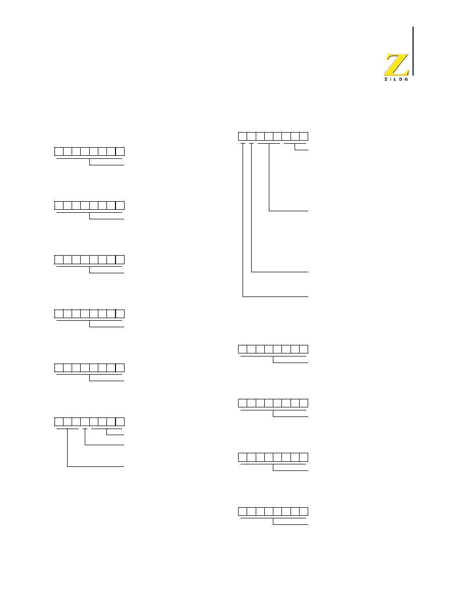
PS019915-1005
Control Register Summary
Z8 Encore!
�
64K Series
Z8 Encore!
26
Control Register Summary
Timer 0 High Byte
T0H (F00H - Read/Write)
D7 D6 D5 D4 D3 D2 D1 D0
Timer 0 current count value [15:8]
Timer 0 Low Byte
T0L (F01H - Read/Write)
D7 D6 D5 D4 D3 D2 D1 D0
Timer 0 current count value [7:0]
Timer 0 Reload High Byte
T0RH (F02H - Read/Write)
D7 D6 D5 D4 D3 D2 D1 D0
Timer 0 reload value [15:8]
Timer 0 Reload Low Byte
T0RL (HF03 - Read/Write)
D7 D6 D5 D4 D3 D2 D1 D0
Timer 0 reload value [7:0]
Timer 0 PWM High Byte
T0PWMH (F04H - Read/Write)
D7 D6 D5 D4 D3 D2 D1 D0
Timer 0 PWM value [15:8]
Timer 0 Control 0
T0CTL0 (F06H - Read/Write)
D7 D6 D5 D4 D3 D2 D1 D0
Reserved
Cascade Timer
0 = Timer 0 Input signal is GPIO pin
1 = Timer 0 Input signal is Timer 3 out
Reserved
Timer 0 Control 1
T0CTL1 (F07H - Read/Write)
D7 D6 D5 D4 D3 D2 D1 D0
Timer Mode
000 = One-Shot mode
001 = CONTINUOUS mode
010 = COUNTER mode
011 = PWM mode
100 = CAPTURE mode
101 = COMPARE mode
110 = GATED mode
111 = Capture/COMPARE mode
Prescale Value
000 = Divide by 1
001 = Divide by 2
010 = Divide by 4
011 = Divide by 8
100 = Divide by 16
101 = Divide by 32
110 = Divide by 64
111 = Divide by 128
Timer Input/Output Polarity
Operation of this bit is a function of
the current operating mode of the timer
Timer Enable
0 = Timer is disabled
1 = Timer is enabled
Timer 1 High Byte
T1H (F08H - Read/Write)
D7 D6 D5 D4 D3 D2 D1 D0
Timer 1 current count value [15:8]
Timer 1 Low Byte
T1L (F09H - Read/Write)
D7 D6 D5 D4 D3 D2 D1 D0
Timer 1 current count value [7:0]
Timer 1 Reload High Byte
T1RH (F0AH - Read/Write)
D7 D6 D5 D4 D3 D2 D1 D0
Timer 1 reload value [15:8]
Timer 1 Reload Low Byte
T1RL (F0BH - Read/Write)
D7 D6 D5 D4 D3 D2 D1 D0
Timer 1 reload value [7:0]
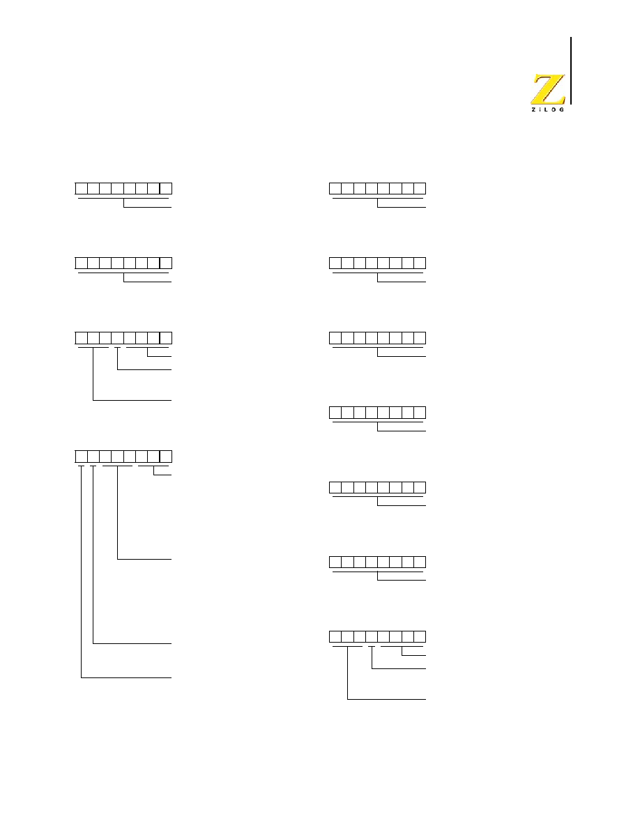
PS019915-1005
Control Register Summary
Z8 Encore!
�
64K Series
Z8 Encore!
27
Timer 1 PWM High Byte
T1PWMH (F0CH - Read/Write)
D7 D6 D5 D4 D3 D2 D1 D0
Timer 1 PWM value [15:8]
Timer 1 PWM Low Byte
T1PWML (F0DH - Read/Write)
D7 D6 D5 D4 D3 D2 D1 D0
Timer 1 PWM value [7:0]
Timer 1 Control 0
T1CTL0 (F0EH - Read/Write)
D7 D6 D5 D4 D3 D2 D1 D0
Reserved
Cascade Timer
0 = Timer 1 Input signal is GPIO pin
1 = Timer 1 Input signal is Timer 0 out
Reserved
Timer 1 Control 1
T1CTL1 (F0FH - Read/Write)
D7 D6 D5 D4 D3 D2 D1 D0
Timer Mode
000 = One-Shot mode
001 = CONTINUOUS mode
010 = COUNTER mode
011 = PWM mode
100 = CAPTURE mode
101 = COMPARE mode
110 = GATED mode
111 = Capture/COMPARE mode
Prescale Value
000 = Divide by 1
001 = Divide by 2
010 = Divide by 4
011 = Divide by 8
100 = Divide by 16
101 = Divide by 32
110 = Divide by 64
111 = Divide by 128
Timer Input/Output Polarity
Operation of this bit is a function of
the current operating mode of the timer
Timer Enable
0 = Timer is disabled
1 = Timer is enabled
Timer 2 High Byte
T2H (F10H - Read/Write)
D7 D6 D5 D4 D3 D2 D1 D0
Timer 2 current count value [15:8]
Timer 2 Low Byte
T2L (F11H - Read/Write)
D7 D6 D5 D4 D3 D2 D1 D0
Timer 2 current count value [7:0]
Timer 2 Reload High Byte
T2RH (F12H - Read/Write)
D7 D6 D5 D4 D3 D2 D1 D0
Timer 2 reload value [15:8]
Timer 2 Reload Low Byte
T2RL (F13H- Read/Write)
D7 D6 D5 D4 D3 D2 D1 D0
Timer 2 reload value [7:0]
Timer 2 PWM High Byte
T2PWMH (F14H - Read/Write)
D7 D6 D5 D4 D3 D2 D1 D0
Timer 2 PWM value [15:8]
Timer 2 PWM Low Byte
T2PWML (F15H - Read/Write)
D7 D6 D5 D4 D3 D2 D1 D0
Timer 2 PWM value [7:0]
Timer 2 Control 0
T2CTL0 (F16H - Read/Write)
D7 D6 D5 D4 D3 D2 D1 D0
Reserved
Cascade Timer
0 = Timer 2 Input signal is GPIO pin
1 = Timer 2 Input signal is Timer 1 out
Reserved
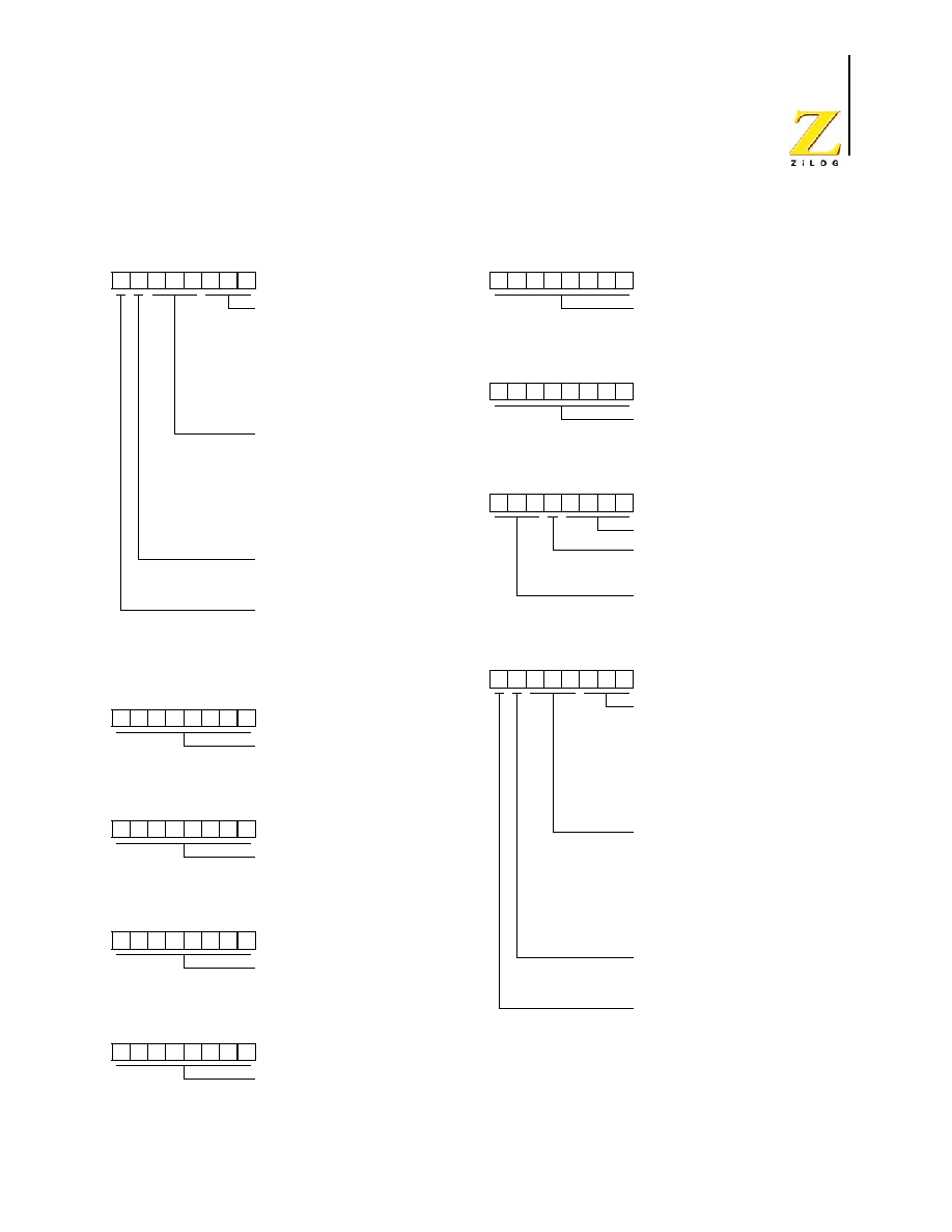
PS019915-1005
Control Register Summary
Z8 Encore!
�
64K Series
Z8 Encore!
28
Timer 2 Control 1
T2CTL1 (F17H - Read/Write)
D7 D6 D5 D4 D3 D2 D1 D0
Timer Mode
000 = One-Shot mode
001 = CONTINUOUS mode
010 = COUNTER mode
011 = PWM mode
100 = CAPTURE mode
101 = COMPARE mode
110 = GATED mode
111 = CAPTURE/COMPARE mode
Prescale Value
000 = Divide by 1
001 = Divide by 2
010 = Divide by 4
011 = Divide by 8
100 = Divide by 16
101 = Divide by 32
110 = Divide by 64
111 = Divide by 128
Timer Input/Output Polarity
Operation of this bit is a function of
the current operating mode of the timer
Timer Enable
0 = Timer is disabled
1 = Timer is enabled
Timer 3 High Byte
T3H (F18H - Read/Write)
D7 D6 D5 D4 D3 D2 D1 D0
Timer 3 current count value [15:8]
Timer 3 Low Byte
T3L (F19H - Read/Write)
D7 D6 D5 D4 D3 D2 D1 D0
Timer 3 current count value [7:0]
Timer 3 Reload High Byte
T3RH (F1AH - Read/Write)
D7 D6 D5 D4 D3 D2 D1 D0
Timer 3 reload value [15:8]
Timer 3 Reload Low Byte
T3RL (F1BH - Read/Write)
D7 D6 D5 D4 D3 D2 D1 D0
Timer 3 reload value [7:0]
Timer 3 PWM High Byte
T3PWMH (F1CH - Read/Write)
D7 D6 D5 D4 D3 D2 D1 D0
Timer 3 PWM value [15:8]
Timer 3 PWM Low Byte
T3PWML (F1DH - Read/Write)
D7 D6 D5 D4 D3 D2 D1 D0
Timer 3 PWM value [7:0]
Timer 3 Control 0
T3CTL0 (F1EH - Read/Write)
D7 D6 D5 D4 D3 D2 D1 D0
Reserved
Cascade Timer
0 = Timer 3 Input signal is GPIO pin
1 = Timer 3 Input signal is Timer 2 out
Reserved
Timer 3 Control 1
T3CTL1 (F1FH - Read/Write)
D7 D6 D5 D4 D3 D2 D1 D0
Timer Mode
000 = One-Shot mode
001 = CONTINUOUS mode
010 = COUNTER mode
011 = PWM mode
100 = CAPTURE mode
101 = COMPARE mode
110 = GATED mode
111 = Capture/COMPARE mode
Prescale Value
000 = Divide by 1
001 = Divide by 2
010 = Divide by 4
011 = Divide by 8
100 = Divide by 16
101 = Divide by 32
110 = Divide by 64
111 = Divide by 128
Timer Input/Output Polarity
Operation of this bit is a function of
the current operating mode of the timer
Timer Enable
0 = Timer is disabled
1 = Timer is enabled
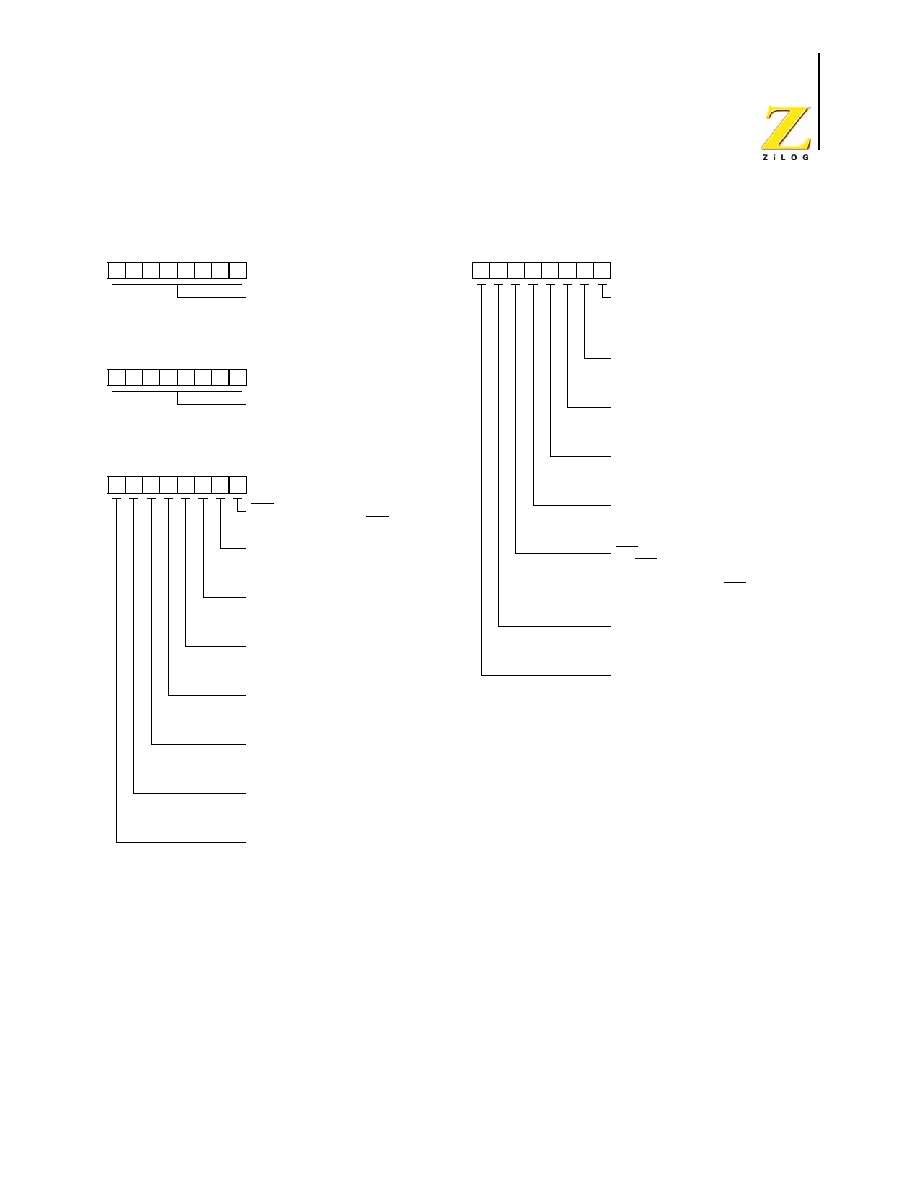
PS019915-1005
Control Register Summary
Z8 Encore!
�
64K Series
Z8 Encore!
29
UART0 Transmit Data
U0TXD (F40H - Write Only)
D7 D6 D5 D4 D3 D2 D1 D0
UART0 transmitter data byte [7:0]
UART0 Receive Data
U0RXD (F40H - Read Only)
D7 D6 D5 D4 D3 D2 D1 D0
UART0 receiver data byte [7:0]
UART0 Status 0
U0STAT0 (F41H - Read Only)
D7 D6 D5 D4 D3 D2 D1 D0
CTS signal
Returns the level of the CTS signal
Transmitter Empty
0 = Data is currently transmitting
1 = Transmission is complete
Transmitter Data Register Empty
0 = Transmit Data Register is full
1 = Transmit Data register is empty
Break Detect
0 = No break occurred
1 = A break occurred
Framing Error
0 = No framing error occurred
1 = A framing occurred
Overrun Error
0 = No overrun error occurred
1 = An overrun error occurred
Parity Error
0 = No parity error occurred
1 = A parity error occurred
Receive Data Available
0 = Receive Data Register is empty
1 = A byte is available in the Receive
Data Register
UART0 Control 0
U0CTL0 (F42H - Read/Write)
D7 D6 D5 D4 D3 D2 D1 D0
Loop Back Enable
0 = Normal operation
1 = Transmit data is looped back to
the receiver
Stop Bit Select
0 = Transmitter sends 1 Stop bit
1 = Transmitter sends 2 Stop bits
Send Break
0 = No break is sent
1 = Output of the transmitter is zero
Parity Select
0 = Even parity
1 = Odd parity
Parity Enable
0 = Parity is disabled
1 = Parity is enabled
CTS Enable
0 = CTS signal has no effect on the
transmitter
1 = UART recognizes CTS signal as a
transmit enable control signal
Receive Enable
0 = Receiver disabled
1 = Receiver enabled
Transmit Enable
0 = Transmitter disabled
1 = Transmitter enabled
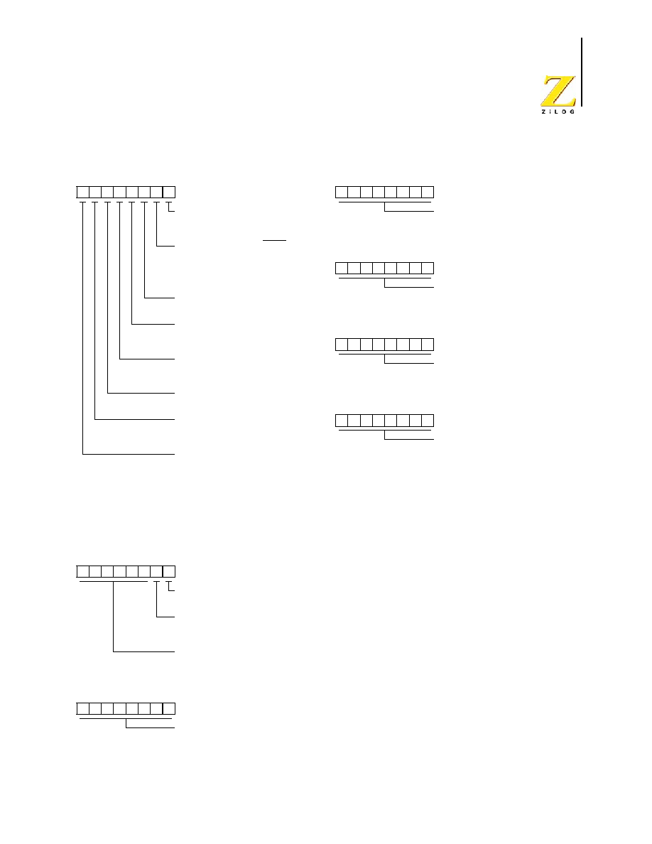
PS019915-1005
Control Register Summary
Z8 Encore!
�
64K Series
Z8 Encore!
30
UART0 Control 1
U0CTL1 (F43H - Read/Write)
D7 D6 D5 D4 D3 D2 D1 D0
Infrared Encoder/Decoder Enable
0 = Infrared endec is disabled
1 = Infrared endec is enabled
Received Data Interrupt Enable
0 = Received data and errors generate
interrupt requests
1 = Only errors generate interrupt
requests. Received data does not.
Baud Rate Registers Control
Refer to UART chapter for operation
Driver Enable Polarity
0 = DE signal is active High
1 = DE signal is active Low
Multiprocessor Bit Transmit
0 = Send a 0 as the multiprocessor bit
1 = Send a 1 as the multiprocessor bit
Multiprocessor Mode [0]
See Multiprocessor Mode [1] below
Multiprocessor (9-bit) Enable
0 = Multiprocessor mode is disabled
1 = Multiprocessor mode is enabled
Multiprocessor Mode [1]
with Multiprocess Mode bit 0:
00 = Interrupt on all received bytes
01 = Interrupt only on address bytes
10 = Interrupt on address match and
following data
11 = Interrupt on data following an
address match
UART0 Status 1
U0STAT1 (F44H - Read Only)
D7 D6 D5 D4 D3 D2 D1 D0
Mulitprocessor Receive
Returns value of last multiprocessor bit
New Frame
0 = Current byte is not start of frame
1 = Current byte is start of new frame
Reserved
UART0 Address Compare
U0ADDR (F45H - Read/Write)
D7 D6 D5 D4 D3 D2 D1 D0
UART0 Address Compare [7:0]
UART0 Baud Rate Generator High Byte
U0BRH (F46H - Read/Write)
D7 D6 D5 D4 D3 D2 D1 D0
UART0 Baud Rate divisor [15:8]
UART0 Baud Rate Generator Low Byte
U0BRL (F47H - Read/Write)
D7 D6 D5 D4 D3 D2 D1 D0
UART0 Baud Rate divisor [7:0]
UART1 Transmit Data
U1TXD (F48H - Write Only)
D7 D6 D5 D4 D3 D2 D1 D0
UART1 transmitter data byte[7:0]
UART1 Receive Data
U1RXD (F48H - Read Only)
D7 D6 D5 D4 D3 D2 D1 D0
UART receiver data byte [7:0]
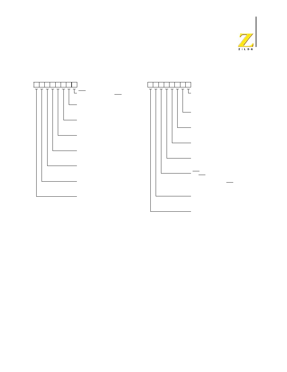
PS019915-1005
Control Register Summary
Z8 Encore!
�
64K Series
Z8 Encore!
31
UART1 Status 0
U1STAT0 (F49H - Read Only)
D7 D6 D5 D4 D3 D2 D1 D0
CTS signal
Returns the level of the CTS signal
Transmitter Empty
0 = Data is currently transmitting
1 = Transmission is complete
Transmitter Data Register Empty
0 = Transmit Data Register is full
1 = Transmit Data register is empty
Break Detect
0 = No break occurred
1 = A break occurred
Framing Error
0 = No framing error occurred
1 = A framing occurred
Overrun Error
0 = No overrun error occurred
1 = An overrun error occurred
Parity Error
0 = No parity error occurred
1 = A parity error occurred
Receive Data Available
0 = Receive Data Register is empty
1 = A byte is available in the Receive
Data Register
UART1 Control 0
U1CTL0 (F4AH - Read/Write)
D7 D6 D5 D4 D3 D2 D1 D0
Loop Back Enable
0 = Normal operation
1 = Transmit data is looped back to
the receiver
Stop Bit Select
0 = Transmitter sends 1 Stop bit
1 = Transmitter sends 2 Stop bits
Send Break
0 = No break is sent
1 = Output of the transmitter is zero
Parity Select
0 = Even parity
1 = Odd parity
Parity Enable
0 = Parity is disabled
1 = Parity is enabled
CTS Enable
0 = CTS signal has no effect on the
transmitter
1 = UART recognizes CTS signal as a
transmit enable control signal
Receive Enable
0 = Receiver disabled
1 = Receiver enabled
Transmit Enable
0 = Transmitter disabled
1 = Transmitter enabled
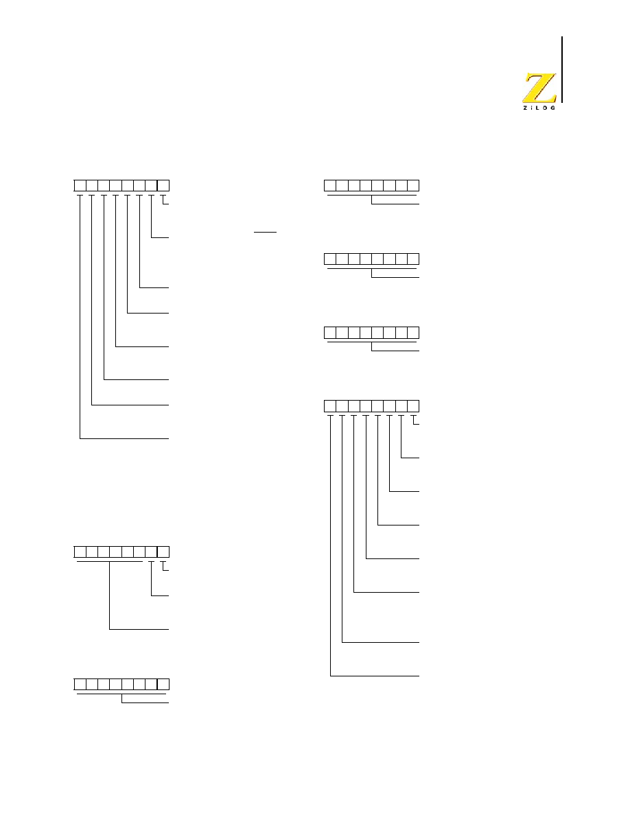
PS019915-1005
Control Register Summary
Z8 Encore!
�
64K Series
Z8 Encore!
32
UART1 Control 1
U0CTL1 (F4BH - Read/Write)
D7 D6 D5 D4 D3 D2 D1 D0
Infrared Encoder/Decoder Enable
0 = Infrared endec is disabled
1 = Infrared endec is enabled
Received Data Interrupt Enable
0 = Received data and errors generate
interrupt requests
1 = Only errors generate interrupt
requests. Received data does not.
Baud Rate Registers Control
Refer to UART chapter for operation
Driver Enable Polarity
0 = DE signal is active High
1 = DE signal is active Low
Multiprocessor Bit Transmit
0 = Send a 0 as the multiprocessor bit
1 = Send a 1 as the multiprocessor bit
Multiprocessor Mode [0]
See Multiprocessor Mode [1] below
Multiprocessor (9-bit) Enable
0 = Multiprocessor mode is disabled
1 = Multiprocessor mode is enabled
Multiprocessor Mode [1]
with Multiprocess Mode bit 0:
00 = Interrupt on all received bytes
01 = Interrupt only on address bytes
10 = Interrupt on address match and
following data
11 = Interrupt on data following an
address match
UART1 Status 1
U0STAT1 (F4CH - Read Only)
D7 D6 D5 D4 D3 D2 D1 D0
Mulitprocessor Receive
Returns value of last multiprocessor bit
New Frame
0 = Current byte is not start of frame
1 = Current byte is start of new frame
Reserved
UART1 Address Compare
U0ADDR (F4DH - Read/Write)
D7 D6 D5 D4 D3 D2 D1 D0
UART1 Address Compare [7:0]
UART1 Baud Rate Generator High Byte
U0BRH (F4EH - Read/Write)
D7 D6 D5 D4 D3 D2 D1 D0
UART1 Baud Rate divisor [15:8]
UART1 Baud Rate Generator Low Byte
U1BRL (F4FH - Read/Write)
D7 D6 D5 D4 D3 D2 D1 D0
UART1 Baud Rate divisor [7:0]
I2C Data
I2CDATA (F50H - Read/Write)
D7 D6 D5 D4 D3 D2 D1 D0
I2C data [7:0]
I2C Status
I2CSTAT (F51H - Read Only)
D7 D6 D5 D4 D3 D2 D1 D0
NACK Interrupt
0 = No action required to service NAK
1 = START/STOP not set after NAK
Data Shift State
0 = Data is not being transferred
1 = Data is being transferred
Transmit Address State
0 = Address is not being transferred
1 = Address is being transferred
Read
0 = Write operation
1 = Read operation
10-Bit Address
0 = 7-bit address being transmitted
1 = 10-bit address being transmitted
Acknowledge
0 = Acknowledge not
transmitted/received
1 = For last byte, Acknowledge was
transmitted/received
Receive Data Register Full
0 = I2C has not received data
1 = Data register contains received data
Transmit Data Register Empty
0 = Data register is full
1 = Data register is empty
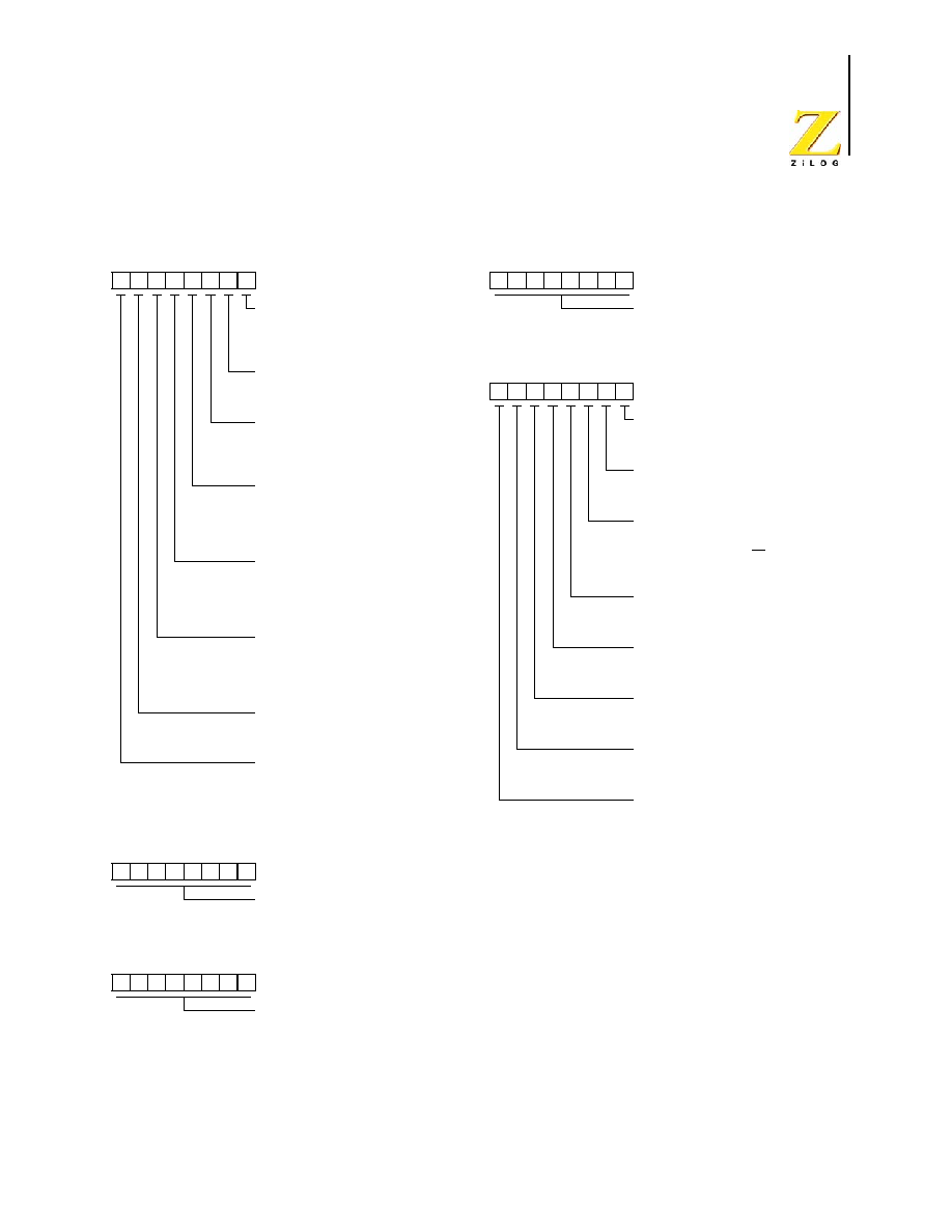
PS019915-1005
Control Register Summary
Z8 Encore!
�
64K Series
Z8 Encore!
33
I2C Control
I2CCTL (F52H - Read/Write)
D7 D6 D5 D4 D3 D2 D1 D0
I2C Signal Filter Enable
0 = Digital filtering disabled
1 = Low-pass digital filters enabled
on SDA and SCL input signals
Flush Data
0 = No effect
1 = Clears I2C Data register
Send NAK
0 = Do not send NAK
1 = Send NAK after next byte received
from slave
Enable TDRE Interrupts
0 = Do not generate an interrupt when
the I2C Data register is empty
1 = Generate an interrupt when the I2C
Transmit Data register is empty
Baud Rate Generator Interrupt Request
0 = Interrupts behave as set by I2C
control
1 = BRG generates an interrupt when
it counts down to zero
Send Stop Condition
0 = Do not issue Stop condition after
data transmission is complete
1 = Issue Stop condition after data
transmission is complete
Send Start Condition
0 = Do not send Start Condition
1 = Send Start Condition
I2C Enable
0 = I2C is disabled
1 = I2C is enabled
I2C Baud Rate Generator High Byte
I2CBRH (F53H - Read/Write)
D7 D6 D5 D4 D3 D2 D1 D0
I2C Baud Rate divisor [15:8]
I2C Baud Rate Generator Low Byte
I2CBRL (F54H - Read/Write)
D7 D6 D5 D4 D3 D2 D1 D0
I2C Baud Rate divisor [7:0]
SPI Data
SPIDATA (F60H - Read/Write)
D7 D6 D5 D4 D3 D2 D1 D0
SPI Data [7:0]
SPI Control
SPICTL (F61H - Read/Write)
D7 D6 D5 D4 D3 D2 D1 D0
SPI Enable
0 = SPI disabled
1 = SPI enabled
Master Mode Enabled
0 = SPI configured in Slave mode
1 = SPI configured in Master mode
Wire-OR (open-drain) Mode Enabled
0 = SPI signals not configured for
open-drain
1 = SPI signals (SCK, SS, MISO, and
MOSI) configured for open-drain
Clock Polarity
0 = SCK idles Low
1 = SPI idles High
Phase Select
Sets the phase relationship of the data
to the clock.
BRG Timer Interrupt Request
0 = BRG timer function is disabled
1 = BRG time-out interrupt is enabled
Start an SPI Interrupt Request
0 = No effect
1 = Generate an SPI interrupt request
Interrupt Request Enable
0 = SPI interrupt requests are disabled
1 = SPI interrupt requests are enabled
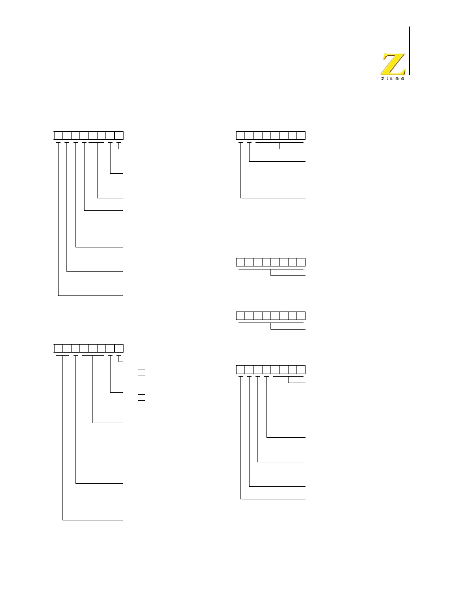
PS019915-1005
Control Register Summary
Z8 Encore!
�
64K Series
Z8 Encore!
34
SPI Status
SPISTAT (F62H - Read Only)
D7 D6 D5 D4 D3 D2 D1 D0
Slave Select
0 = If Slave, SS pin is asserted
1 = If Slave, SS pin is not asserted
Transmit Status
0 = No data transmission in progress
1 = Data transmission now in progress
Reserved
Slave Mode Transaction Abort
0 = No slave mode transaction abort
detected
1 = Slave mode transaction abort was
detected
Collision
0 = No multi-master collision detected
1 = Multi-master collision was detected
Overrun
0 = No overrun error detected
1 = Overrun error was detected
Interrupt Request
0 = No SPI interrupt request pending
1 = SPI interrupt request is pending
SPI Mode
SPIMODE (F63H - Read/Write)
D7 D6 D5 D4 D3 D2 D1 D0
Slave Select Value
If Master and SPIMODE[1] = 1:
0 = SS pin driven Low
1 = SS pin driven High
Slave Select I/O
0 = SS pin configured as an input
1 = SS pin configured as an output
(Master mode only)
Number of Data Bits Per Character
000 = 8 bits
001 = 1 bit
010 = 2 bits
011 = 3 bits
100 = 4 bits
101 = 5 bit
110 = 6 bits
111 = 7 bits
Diagnostic Mode Control
0 = Reading from SPIBRH, SPIBRL
returns reload values
1 = Reading from SPIBRH, SPIBRL
returns current BRG count value
Reserved
SPI Diagnostic State
SPIDST (F64H - Read Only)
D7 D6 D5 D4 D3 D2 D1 D0
SPI State
Transmit Clock Enable
0 = Internal transmit clock enable
signal is deasserted
1 = Internal transmit clock enable
signal is asserted
Shift Clock Enable
0 = Internal shift clock enable signal
is deasserted
1 = Internal shift clock enable signal
is asserted
SPI Baud Rate Generator High Byte
SPIBRH (F66H - Read/Write)
D7 D6 D5 D4 D3 D2 D1 D0
SPI Baud Rate divisor [15:8]
SPI Baud Rate Generator Low Byte
SPIBRL (F67H - Read/Write)
D7 D6 D5 D4 D3 D2 D1 D0
SPI Baud Rate divisor [7:0]
ADC Control
ADCCTL (F70H - Read/Write)
D7 D6 D5 D4 D3 D2 D1 D0
Analog Input Select
0000 = ANA0 0001 = ANA1
0010 = ANA2 0011 = ANA3
0100 = ANA4 0101 = ANA5
0110 = ANA6 0111 = ANA7
1000 = ANA8 1001 = ANA9
1010 = ANA10 1011 = ANA11
11xx = Reserved
Continuous Mode Select
0 = Single-shot conversion
1 = Continuous conversion
External VREF select
0 = Internal voltage reference selected
1 = External voltage reference selected
Reserved
Conversion Enable
0 = Conversion is complete
1 = Begin conversion
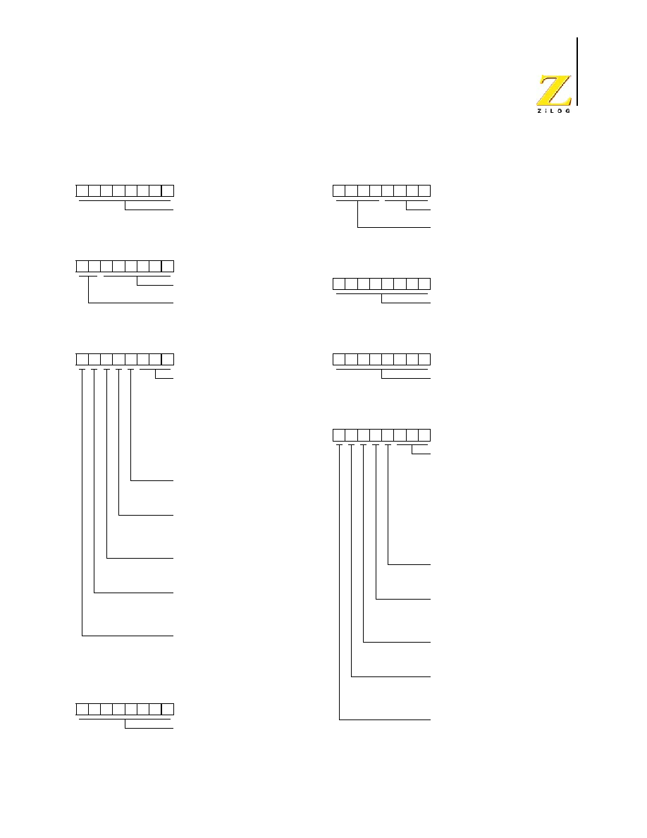
PS019915-1005
Control Register Summary
Z8 Encore!
�
64K Series
Z8 Encore!
35
ADC Data High Byte
ADCD_H (F72H - Read Only)
D7 D6 D5 D4 D3 D2 D1 D0
ADC Data [9:2]
ADC Data Low Bits
ADCD_L (F73H - Read Only)
D7 D6 D5 D4 D3 D2 D1 D0
Reserved
ADC Data [1:0]
DMA0 Control
DMA0CTL (FB0H - Read/Write)
D7 D6 D5 D4 D3 D2 D1 D0
Request Trigger Source Select
000 = Timer 0
001 = Timer 1
010 = Timer 2
011 = Timer 3
100 = UART0 Received Data register
contains valid data
101 = UART1 Received Data register
contains valid data
110 = I2C receiver contains valid data
111 = Reserved
Word Select
0 = DMA transfers 1 byte per request
1 = DMA transfers 2 bytes per request
DMA0 Interrupt Enable
0 = DMA0 does not generate interrupts
1 = DMA0 generates an interrupt when
End Address data is transferred
DMA0 Data Transfer Direction
0 = Register File to peripheral registers
1 = Peripheral registers to Register File
DMA0 Loop Enable
0 = DMA disables after End Address
1 = DMA reloads Start Address after
End Address and continues to run
DMA0 Enable
0 = DMA0 is disabled
1 = DMA0 is enabled
DMA0 I/O Address
DMA0IO (FB1H - Read/Write)
D7 D6 D5 D4 D3 D2 D1 D0
DMA0 Peripheral Register Address
Low byte of on-chip peripheral control
registers on Register File page FH
DMA0 Address High Nibble
DMA0H (FB2H - Read/Write)
D7 D6 D5 D4 D3 D2 D1 D0
DMA0 Start Address [11:8]
DMA0 End Address [11:8]
DMA0 Start/Current Address Low Byte
DMA0START (FB3H - Read/Write)
D7 D6 D5 D4 D3 D2 D1 D0
DMA0 Start Address [7:0]
DMA0 End Address Low Byte
DMA0END (FB4H - Read/Write)
D7 D6 D5 D4 D3 D2 D1 D0
DMA0 End Address [7:0]
DMA1 Control
DMA1CTL (FB8H - Read/Write)
D7 D6 D5 D4 D3 D2 D1 D0
Request Trigger Source Select
000 = Timer 0
001 = Timer 1
010 = Timer 2
011 = Timer 3
100 = UART0 Transmit Data register
is empty
101 = UART1 Transmit Data register
is empty
110 = I2C Transmit Data register
is empty
111 = Reserved
Word Select
0 = DMA transfers 1 byte per request
1 = DMA transfers 2 bytes per request
DMA1 Interrupt Enable
0 = DMA1 does not generate interrupts
1 = DMA1 generates an interrupt when
End Address data is transferred
DMA1 Data Transfer Direction
0 = Register File to peripheral registers
1 = Peripheral registers to Register File
DMA1 Loop Enable
0 = DMA disables after End Address
1 = DMA reloads Start Address after
End Address and continues to run
DMA1 Enable
0 = DMA1 is disabled
1 = DMA1 is enabled
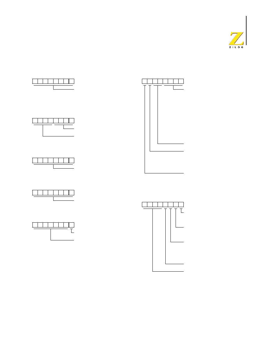
PS019915-1005
Control Register Summary
Z8 Encore!
�
64K Series
Z8 Encore!
36
DMA1 I/O Address
DMA1IO (FB9H - Read/Write)
D7 D6 D5 D4 D3 D2 D1 D0
DMA1 Peripheral Register Address
Low byte of on-chip peripheral control
registers on Register File page FH
DMA1 Address High Nibble
DMA1H (FBAH - Read/Write)
D7 D6 D5 D4 D3 D2 D1 D0
DMA1 Start Address [11:8]
DMA1 End Address [11:8]
DMA1 Start/Current Address Low Byte
DMA1START (FBBH - Read/Write)
D7 D6 D5 D4 D3 D2 D1 D0
DMA1 Start Address [7:0]
DMA1 End Address Low Byte
DMA1END (FBCH - Read/Write)
D7 D6 D5 D4 D3 D2 D1 D0
DMA1 End Address [7:0]
DMA_ADC Address
DMAA_ADDR (FBDH - Read/Write)
D7 D6 D5 D4 D3 D2 D1 D0
Reserved
DMA_ADC Address
DMA_ADC Control
DMAACTL (FBEH - Read/Write)
D7 D6 D5 D4 D3 D2 D1 D0
ADC Analog Input Number
0000 = Analog input 0 updated
0001 = Analog input 0-1 updated
0010 = Analog input 0-2 updated
0011 = Analog input 0-3 updated
0100 = Analog input 0-4 updated
0101 = Analog input 0-5 updated
0100 = Analog input 0-6 updated
0101 = Analog input 0-7 updated
1000 = Analog input 0-8 updated
1001 = Analog input 0-9 updated
1010 = Analog input 0-10 updated
1011 = Analog inputs 0-11 updated
11xx = Reserved
Reserved
Interrupt request enable
0 = DMA_ADC does not generate
interrupt requests
1 = DMA_ADC generates interrupt
requests after last analog input
DMA_ADC Enable
0 = DMA_ADC is disabled
1 = DMA_ADC is enabled
DMA Status
DMAA_STAT (FBFH - Read Only)
D7 D6 D5 D4 D3 D2 D1 D0
DMA0 Interrupt Request Indicator
0 = DMA0 is not the source of the IRQ
1 = DMA0 is the source of the IRQ
DMA1 Interrupt Request Indicator
0 = DMA1 is not the source of the IRQ
1 = DMA1 is the source of the IRQ
DMA_ADC Interrupt Request Indicator
0 = DMA_ADC is not the source of the
IRQ
1 = DMA_ADC is the source of the
IRQ
Reserved
Current ADC analog input
Identifies the analog input the ADC is
currently converting
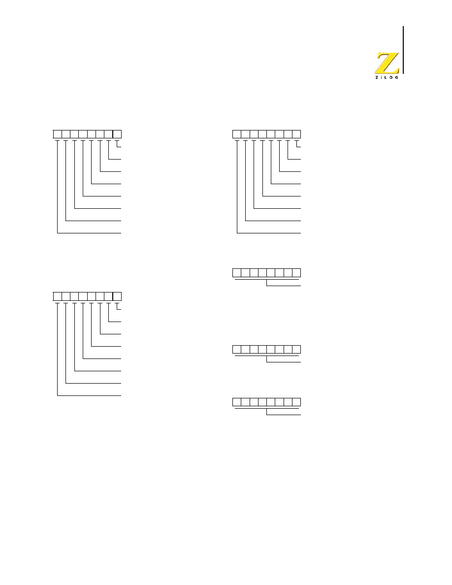
PS019915-1005
Control Register Summary
Z8 Encore!
�
64K Series
Z8 Encore!
37
Interrupt Request 0
IRQ0 (FC0H - Read/Write)
D7 D6 D5 D4 D3 D2 D1 D0
ADC Interrupt Request
SPI Interrupt Request
I2C Interrupt Request
UART 0 Transmitter Interrupt Request
UART 0 Receiver Interrupt Request
Timer 0 Interrupt Request
Timer 1 Interrupt Request
Timer 2 Interrupt Request
For all of the above peripherals:
0 = Peripheral IRQ is not pending
1 = Peripheral IRQ is awaiting service
IRQ0 Enable High Bit
IRQ0ENH (FC1H - Read/Write)
D7 D6 D5 D4 D3 D2 D1 D0
ADC IRQ Enable Hit Bit
SPI IRQ Enable High Bit
I2C IRQ Enable High Bit
UART 0 Transmitter IRQ Enable High
UART 0 Receiver IRQ Enable High Bit
Timer 0 IRQ Enable High Bit
Timer 1 IRQ Enable High Bit
Timer 2 IRQ Enable High Bit
IRQ0 Enable Low Bit
IRQ0ENL (FC2H - Read/Write)
D7 D6 D5 D4 D3 D2 D1 D0
ADC IRQ Enable Hit Bit
SPI IRQ Enable Low Bit
I2C IRQ Enable Low Bit
UART 0 Transmitter IRQ Enable Low
UART 0 Receiver IRQ Enable Low Bit
Timer 0 IRQ Enable Low Bit
Timer 1 IRQ Enable Low Bit
Timer 2 IRQ Enable Low Bit
Interrupt Request 1
IRQ1 (FC3H - Read/Write)
D7 D6 D5 D4 D3 D2 D1 D0
Port A or D Pin Interrupt Request
0 = IRQ from corresponding pin [7:0]
is not pending
1 = IRQ from corresponding pin [7:0]
is awaiting service
IRQ1 Enable High Bit
IRQ1ENH (FC4H - Read/Write)
D7 D6 D5 D4 D3 D2 D1 D0
Port A or D Pin IRQ Enable High Bit
IRQ1 Enable Low Bit
IRQ1ENL (FC5H - Read/Write)
D7 D6 D5 D4 D3 D2 D1 D0
Port A or D Pin IRQ Enable Low Bit
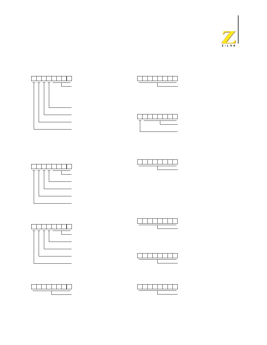
PS019915-1005
Control Register Summary
Z8 Encore!
�
64K Series
Z8 Encore!
38
Interrupt Request 2
IRQ2 (FC6H - Read/Write)
D7 D6 D5 D4 D3 D2 D1 D0
Port C Pin Interrupt Request
0 = IRQ from corresponding pin [3:0]
is not pending
1 = IRQ from corresponding pin [3:0]
is awaiting service
DMA Interrupt Request
UART 1 Transmitter Interrupt Request
UART 1 Receiver Interrupt Request
Timer 3 Interrupt Request
For all of the above peripherals:
0 = Peripheral IRQ is not pending
1 = Peripheral IRQ is awaiting service
IRQ2 Enable High Bit
IRQ2ENH (FC7H - Read/Write)
D7 D6 D5 D4 D3 D2 D1 D0
Port C Pin IRQ Enable High Bit
DMA IRQ Enable High Bit
UART 1 Transmitter IRQ Enable High
UART 1 Receiver IRQ Enable High Bit
Timer 3 IRQ Enable High Bit
IRQ2 Enable Low Bit
IRQ2ENL (FC8H - Read/Write)
D7 D6 D5 D4 D3 D2 D1 D0
Port C Pin IRQ Enable Low Bit
DMA IRQ Enable Low Bit
UART 1 Transmitter IRQ Enable Low
UART 1 Receiver IRQ Enable Low Bit
Timer 3 IRQ Enable Low Bit
Interrupt Edge Select
IRQES (FCDH - Read/Write)
D7 D6 D5 D4 D3 D2 D1 D0
Port A or D Interrupt Edge Select [7:0]
0 = Falling edge
1 = Rising edge
Interrupt Port Select
IRQPS (FCEH - Read/Write)
D7 D6 D5 D4 D3 D2 D1 D0
Port A or D Port Pin Select [7:0]
0 = Port A pin is the interrupt source
1 = Port D pin is the interrupt source
Interrupt Control
IRQCTL (FCFH - Read/Write)
D7 D6 D5 D4 D3 D2 D1 D0
Reserved
Interrupt Request Enable
0 = Interrupts are disabled
1 = Interrupts are enabled
Port A Address
PAADDR (FD0H - Read/Write)
D7 D6 D5 D4 D3 D2 D1 D0
Port A Address[7:0]
Selects Port Sub-Registers:
00H = No function
01H = Data direction
02H = Alternate function
03H = Output control (open-drain)
04H = High drive enable
05H = STOP mode recovery enable
06H-FFH = No function
Port A Control
PACTL (FD1H - Read/Write)
D7 D6 D5 D4 D3 D2 D1 D0
Port A Control[7:0]
Provides Access to Port Sub-Registers
Port A Input Data
PAIN (FD2H - Read Only)
D7 D6 D5 D4 D3 D2 D1 D0
Port A Input Data [7:0]
Port A Output Data
PAOUT (FD3H - Read/Write)
D7 D6 D5 D4 D3 D2 D1 D0
Port A Output Data [7:0]

PS019915-1005
Control Register Summary
Z8 Encore!
�
64K Series
Z8 Encore!
39
Port B Address
PBADDR (FD4H - Read/Write)
D7 D6 D5 D4 D3 D2 D1 D0
Port B Address[7:0]
Selects Port Sub-Registers:
00H = No function
01H = Data direction
02H = Alternate function
03H = Output control (open-drain)
04H = High drive enable
05H = STOP mode recovery enable
06H-FFH = No function
Port B Control
PBCTL (FD5H - Read/Write)
D7 D6 D5 D4 D3 D2 D1 D0
Port B Control[7:0]
Provides Access to Port Sub-Registers
Port B Input Data
PBIN (FD6H - Read Only)
D7 D6 D5 D4 D3 D2 D1 D0
Port B Input Data [7:0]
Port B Output Data
PBOUT (FD7H - Read/Write)
D7 D6 D5 D4 D3 D2 D1 D0
Port B Output Data [7:0]
Port C Address
PCADDR (FD8H - Read/Write)
D7 D6 D5 D4 D3 D2 D1 D0
Port C Address[7:0]
Selects Port Sub-Registers:
00H = No function
01H = Data direction
02H = Alternate function
03H = Output control (open-drain)
04H = High drive enable
05H = STOP mode recovery enable
06H-FFH = No function
Port C Control
PCCTL (FD9H - Read/Write)
D7 D6 D5 D4 D3 D2 D1 D0
Port C Control[7:0]
Provides Access to Port Sub-Registers
Port C Input Data
PCIN (FDAH - Read Only)
D7 D6 D5 D4 D3 D2 D1 D0
Port C Input Data [7:0]
Port C Output Data
PCOUT (FDBH - Read/Write)
D7 D6 D5 D4 D3 D2 D1 D0
Port C Output Data [7:0]
Port D Address
PDADDR (FDCH - Read/Write)
D7 D6 D5 D4 D3 D2 D1 D0
Port D Address[7:0]
Selects Port Sub-Registers:
00H = No function
01H = Data direction
02H = Alternate function
03H = Output control (open-drain)
04H = High drive enable
05H = STOP mode recovery enable
06H-FFH = No function
Port D Control
PDCTL (FDDH - Read/Write)
D7 D6 D5 D4 D3 D2 D1 D0
Port D Control[7:0]
Provides Access to Port Sub-Registers
Port D Input Data
PDIN (FDE H- Read Only)
D7 D6 D5 D4 D3 D2 D1 D0
Port D Input Data [7:0]
Port D Output Data
PDOUT (FDFH - Read/Write)
D7 D6 D5 D4 D3 D2 D1 D0
Port D Output Data [7:0]
PS019915-1005
Control Register Summary
Z8 Encore!
�
64K Series
Z8 Encore!
40
Port E Address
PEADDR (FE0H - Read/Write)
D7 D6 D5 D4 D3 D2 D1 D0
Port E Address[7:0]
Selects Port Sub-Registers:
00H = No function
01H = Data direction
02H = Alternate function
03H = Output control (open-drain)
04H = High drive enable
05H = STOP mode recovery enable
06H-FFH = No function
Port E Control
PECTL (FE1H - Read/Write)
D7 D6 D5 D4 D3 D2 D1 D0
Port E Control[7:0]
Provides Access to Port Sub-Registers
Port E Input Data
PEIN (FE2H - Read Only)
D7 D6 D5 D4 D3 D2 D1 D0
Port E Input Data [7:0]
Port E Output Data
PEOUT (FE3H - Read/Write)
D7 D6 D5 D4 D3 D2 D1 D0
Port E Output Data [7:0]
Port F Address
PFADDR (FE4H - Read/Write)
D7 D6 D5 D4 D3 D2 D1 D0
Port F Address[7:0]
Selects Port Sub-Registers:
00H = No function
01H = Data direction
02H = Alternate function
03H = Output control (open-drain)
04H = High drive enable
05H = STOP mode recovery enable
06H-FFH = No function
Port F Control
PFCTL (FE5H - Read/Write)
D7 D6 D5 D4 D3 D2 D1 D0
Port F Control[7:0]
Provides Access to Port Sub-Registers
Port F Input Data
PFIN (FE6H - Read Only)
D7 D6 D5 D4 D3 D2 D1 D0
Port F Input Data [7:0]
Port F Output Data
PFOUT (FE7H - Read/Write)
D7 D6 D5 D4 D3 D2 D1 D0
Port F Output Data [7:0]
Port G Address
PGADDR (FE8H - Read/Write)
D7 D6 D5 D4 D3 D2 D1 D0
Port G Address[7:0]
Selects Port Sub-Registers:
00H = No function
01H = Data direction
02H = Alternate function
03H = Output control (open-drain)
04H = High drive enable
05H = STOP mode recovery enable
06H-FFH = No function
Port G Control
PGCTL (FE9H - Read/Write)
D7 D6 D5 D4 D3 D2 D1 D0
Port G Control[7:0]
Provides Access to Port Sub-Registers
Port G Input Data
PGIN (FEAH - Read Only)
D7 D6 D5 D4 D3 D2 D1 D0
Port G Input Data [7:0]
Port G Output Data
PGOUT (FEBH - Read/Write)
D7 D6 D5 D4 D3 D2 D1 D0
Port G Output Data [7:0]
PS019915-1005
Control Register Summary
Z8 Encore!
�
64K Series
Z8 Encore!
41
Port H Address
PHADDR (FECH - Read/Write)
D7 D6 D5 D4 D3 D2 D1 D0
Port H Address[7:0]
Selects Port Sub-Registers:
00H = No function
01H = Data direction
02H = Alternate function
03H = Output control (open-drain)
04H = High drive enable
05H = STOP mode recovery enable
06H-FFH = No function
Port H Control
PHCTL (FEDH - Read/Write)
D7 D6 D5 D4 D3 D2 D1 D0
Port H Control [3:0]
Provides Access to Port Sub-Registers
Reserved
Port H Input Data
PHIN (FEEH - Read Only)
D7 D6 D5 D4 D3 D2 D1 D0
Port H Input Data [3:0]
Reserved
Port H Output Data
PHOUT (FEFH - Read/Write)
D7 D6 D5 D4 D3 D2 D1 D0
Port H Output Data [3:0]
Reserved
Watch-Dog Timer Control
WDTCTL (FF0H - Read Only)
D7 D6 D5 D4 D3 D2 D1 D0
SM Configuration Indicator
Reserved
EXT
0 = Reset not generated by RESET pin
1 = Reset generated by RESET pin
WDT
0 = WDT timeout has not occurred
1 = WDT timeout occurred
STOP
0 = SMR has not occurred
1 = SMR has occurred
POR
0 = POR has not occurred
1 = POR has occurred
Watch-Dog Timer Reload Upper Byte
WDTU (FF1H - Read/Write)
D7 D6 D5 D4 D3 D2 D1 D0
WDT reload value [23:16]
Watch-Dog Timer Reload Middle Byte
WDTH (FF2 H- Read/Write)
D7 D6 D5 D4 D3 D2 D1 D0
WDT reload value [15:8]
Watch-Dog Timer Reload Low Byte
WDTL (FF3H - Read/Write)
D7 D6 D5 D4 D3 D2 D1 D0
WDT reload value [7:0]
Flash Control
FCTL (FF8H - Write Only)
D7 D6 D5 D4 D3 D2 D1 D0
Flash Command
73H = First unlock command
8CH = Second unlock command
95H = Page erase command
63H = Mass erase command
5EH = Flash Sector Protect reg select
PS019915-1005
Control Register Summary
Z8 Encore!
�
64K Series
Z8 Encore!
42
Flash Status
FSTAT (FF8H - Read Only)
D7 D6 D5 D4 D3 D2 D1 D0
Flash Controller Status
00_0000 = Flash controller locked
00_0001 = First unlock received
00_0010 = Second unlock received
00_0011 = Flash controller unlocked
00_0100 = Flash Sector Protect register
selected
00_1xxx = Programming in progress
01_0xxx = Page erase in progress
10_0xxx = Mass erase in progress
Reserved
Page Select
FPS (FF9H - Read/Write)
D7 D6 D5 D4 D3 D2 D1 D0
Page Select [6:0]
Identifies the Flash memory page for
Page Erase operation.
Information Area Enable
0 = Information Area access is disabled
1 = Information Area access is enabled
Flash Sector Protect
FPROT (FF9H - Read/Write to 1's)
D7 D6 D5 D4 D3 D2 D1 D0
Flash Sector Protect [7:0]
0 = Sector can be programmed or
erased from user code
1 = Sector is protected and cannot be
programmed or erased from user
code
Flash Frequency High Byte
FFREQH (FFAH - Read/Write)
D7 D6 D5 D4 D3 D2 D1 D0
Flash Frequency value [15:8]
Flash Frequency Low Byte
FFREQL (FFBH - Read/Write)
D7 D6 D5 D4 D3 D2 D1 D0
Flash Frequency value [7:0]
Flags
FLAGS (FFC - Read/Write)
D7 D6 D5 D4 D3 D2 D1 D0
F1 - User Flag 1
F2 - User Flag 2
H - Half Carry
D - Decimal Adjust
V - Overflow Flag
S - Sign Flag
Z - Zero Flag
C - Carry Flag
Register Pointer
RP (FFDH - Read/Write)
D7 D6 D5 D4 D3 D2 D1 D0
Working Register Page Address [11:8]
Working Register Group Address [7:4]
Stack Pointer High Byte
SPH (FFEH - Read/Write)
D7 D6 D5 D4 D3 D2 D1 D0
Stack Pointer [15:8]
Stack Pointer Low Byte
SPL (FFFH - Read/Write)
D7 D6 D5 D4 D3 D2 D1 D0
Stack Pointer [7:0]

Z8 Encore!
�
64K Series
Product Specification
PS019915-1005
Reset and STOP Mode Recovery
43
Reset and STOP Mode Recovery
Overview
The Reset Controller within the Z8 Encore!
�
64K Series controls Reset and STOP Mode
Recovery operation. In typical operation, the following events cause a Reset to occur:
�
Power-On Reset (POR)
�
Voltage Brown-Out (VBO)
�
Watch-Dog Timer time-out (when configured via the WDT_RES Option Bit to initiate
a Reset)
�
External RESET pin assertion
�
On-Chip Debugger initiated Reset (OCDCTL[0] set to 1)
When the 64K Series devices are in STOP mode, a STOP Mode Recovery is initiated by
either of the following:
�
Watch-Dog Timer time-out
�
GPIO Port input pin transition on an enabled STOP Mode Recovery source
�
DBG pin driven Low
Reset Types
The 64K Series provides two different types of reset operation (System Reset and STOP
Mode Recovery). The type of Reset is a function of both the current operating mode of the
64K Series devices and the source of the Reset. Table 8 lists the types of Reset and their
operating characteristics.
Table 8. Reset and STOP Mode Recovery Characteristics and Latency
Reset Type
Reset Characteristics and Latency
Control Registers
eZ8 CPU Reset Latency (Delay)
System Reset
Reset (as applicable)
Reset
66 WDT Oscillator cycles + 16 System Clock cycles
STOP Mode
Recovery
Unaffected, except
WDT_CTL register
Reset
66 WDT Oscillator cycles + 16 System Clock cycles

PS019915-1005
Reset and STOP Mode Recovery
Z8 Encore!
�
64K Series
Product Specification
44
System Reset
During a System Reset, the 64K Series devices are held in Reset for 66 cycles of the
Watch-Dog Timer oscillator followed by 16 cycles of the system clock. At the beginning
of Reset, all GPIO pins are configured as inputs.
During Reset, the eZ8 CPU and on-chip peripherals are idle; however, the on-chip crystal
oscillator and Watch-Dog Timer oscillator continue to run. The system clock begins oper-
ating following the Watch-Dog Timer oscillator cycle count. The eZ8 CPU and on-chip
peripherals remain idle through the 16 cycles of the system clock.
Upon Reset, control registers within the Register File that have a defined Reset value are
loaded with their reset values. Other control registers (including the Stack Pointer, Regis-
ter Pointer, and Flags) and general-purpose RAM are undefined following Reset. The eZ8
CPU fetches the Reset vector at Program Memory addresses
0002H
and
0003H
and loads
that value into the Program Counter. Program execution begins at the Reset vector
address.
Reset Sources
Table 9 lists the reset sources as a function of the operating mode. The text following pro-
vides more detailed information on the individual Reset sources. A Power-On Reset/Volt-
age Brown-Out event always takes priority over all other possible reset sources to ensure a
full system reset occurs.
Power-On Reset
Each device in the 64K Series contains an internal Power-On Reset (POR) circuit. The
POR circuit monitors the supply voltage and holds the device in the Reset state until the
supply voltage reaches a safe operating level. After the supply voltage exceeds the POR
Table 9. Reset Sources and Resulting Reset Type
Operating Mode
Reset Source
Reset Type
Normal or HALT
modes
Power-On Reset / Voltage Brown-Out System Reset
Watch-Dog Timer time-out
when configured for Reset
System Reset
RESET pin assertion
System Reset
On-Chip Debugger initiated Reset
(OCDCTL[0] set to 1)
System Reset except the On-Chip Debugger is
unaffected by the reset
STOP mode
Power-On Reset / Voltage Brown-Out System Reset
RESET pin assertion
System Reset
DBG pin driven Low
System Reset
PS019915-1005
Reset and STOP Mode Recovery
Z8 Encore!
�
64K Series
Product Specification
45
voltage threshold (V
POR
), the POR Counter is enabled and counts 66 cycles of the Watch-
Dog Timer oscillator. After the POR counter times out, the XTAL Counter is enabled to
count a total of 16 system clock pulses. The devices are held in the Reset state until both
the POR Counter and XTAL counter have timed out. After the 64K Series devices exit the
Power-On Reset state, the eZ8 CPU fetches the Reset vector. Following Power-On Reset,
the POR status bit in the Watch-Dog Timer Control (WDTCTL) register is set to 1.
Figure 8 illustrates Power-On Reset operation. Refer to the Electrical Characteristics
chapter for the POR threshold voltage (V
POR
).
Figure 8. Power-On Reset Operation)
Voltage Brown-Out Reset
The devices in the 64K Series provide low Voltage Brown-Out (VBO) protection. The
VBO circuit senses when the supply voltage drops to an unsafe level (below the VBO
threshold voltage) and forces the device into the Reset state. While the supply voltage
remains below the Power-On Reset voltage threshold (V
POR
), the VBO block holds the
device in the Reset state.
After the supply voltage again exceeds the Power-On Reset voltage threshold, the devices
progress through a full System Reset sequence, as described in the Power-On Reset sec-
VCC = 0.0V
VCC = 3.3V
V
POR
V
VBO
Primary
Oscillator
Internal RESET
signal
Program
Execution
Oscillator
Start-up
XTAL
WDT Clock
POR
counter delay
counter delay
Not to Scale
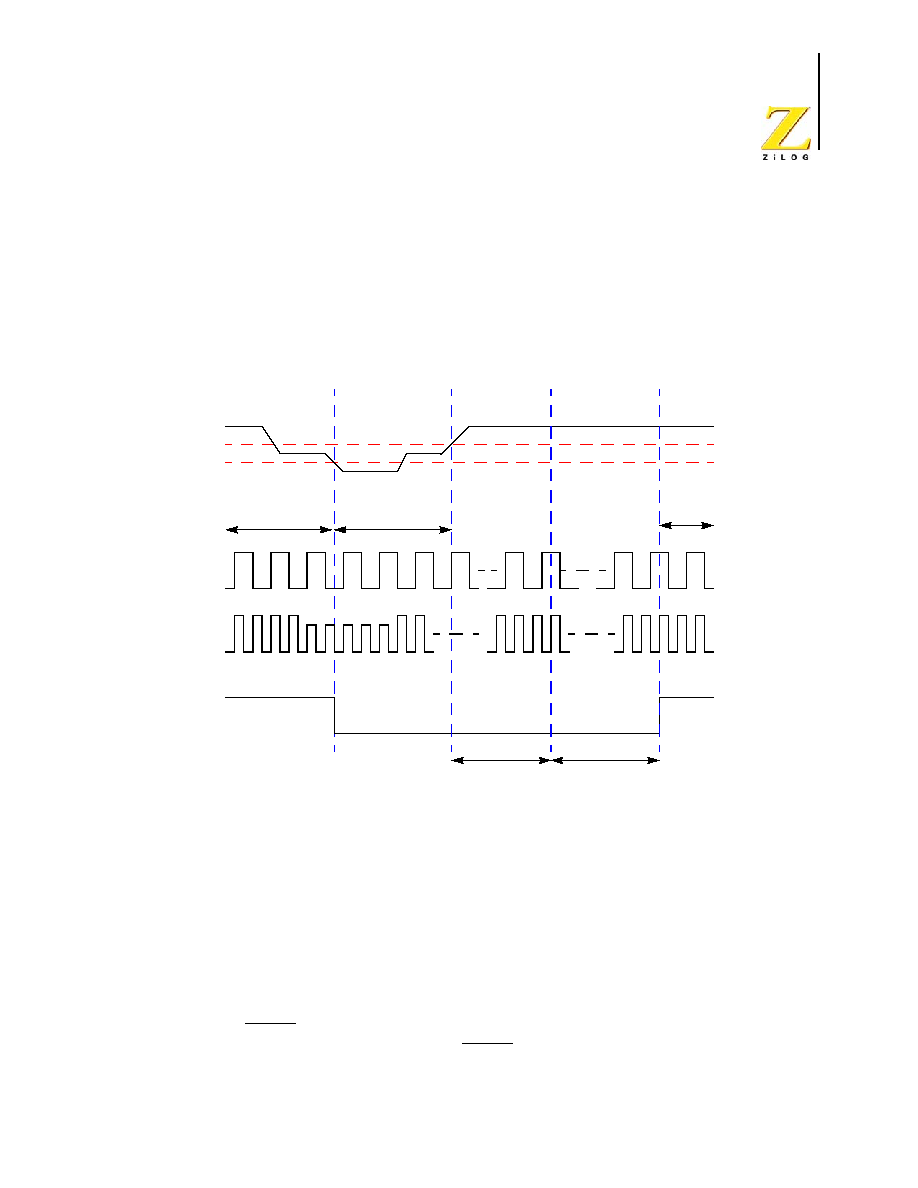
PS019915-1005
Reset and STOP Mode Recovery
Z8 Encore!
�
64K Series
Product Specification
46
tion. Following Power-On Reset, the POR status bit in the Watch-Dog Timer Control
(WDTCTL) register is set to 1. Figure 9 illustrates Voltage Brown-Out operation. Refer to
the Electrical Characteristics chapter for the VBO and POR threshold voltages (V
VBO
and V
POR
).
The Voltage Brown-Out circuit can be either enabled or disabled during STOP mode.
Operation during STOP mode is set by the VBO_AO Option Bit. Refer to the Option Bits
chapter for information on configuring VBO_AO.
Figure 9. Voltage Brown-Out Reset Operation
Watch-Dog Timer Reset
If the device is in normal or HALT mode, the Watch-Dog Timer can initiate a System
Reset at time-out if the WDT_RES Option Bit is set to 1. This capability is the default
(unprogrammed) setting of the WDT_RES Option Bit. The
WDT
status bit in the WDT Con-
trol register is set to signify that the reset was initiated by the Watch-Dog Timer.
External Pin Reset
The RESET pin has a Schmitt-triggered input, an internal pull-up, an analog filter and a
digital filter to reject noise. Once the RESET pin is asserted for at least 4 system clock
VCC = 3.3V
V
POR
V
VBO
Internal RESET
Signal
Program
Execution
Program
Execution
Voltage
Brownout
VCC = 3.3V
Primary
Oscillator
WDT Clock
XTAL
POR
Counter Delay
Counter Delay

PS019915-1005
Reset and STOP Mode Recovery
Z8 Encore!
�
64K Series
Product Specification
47
cycles, the devices progress through the System Reset sequence. While the RESET input
pin is asserted Low, the 64K Series devices continue to be held in the Reset state. If the
RESET pin is held Low beyond the System Reset time-out, the devices exit the Reset state
immediately following RESET pin deassertion. Following a System Reset initiated by the
external RESET pin, the EXT status bit in the Watch-Dog Timer Control (WDTCTL) reg-
ister is set to 1.
On-Chip Debugger Initiated Reset
A Power-On Reset can be initiated using the On-Chip Debugger by setting the
RST
bit in
the OCD Control register. The On-Chip Debugger block is not reset but the rest of the chip
goes through a normal system reset. The
RST
bit automatically clears during the system
reset. Following the system reset the
POR
bit in the WDT Control register is set.
STOP Mode Recovery
STOP mode is entered by the eZ8 executing a
STOP
instruction. Refer to the Section
Low-Power Modes on page 49 for detailed STOP mode information. During STOP Mode
Recovery, the devices are held in reset for 66 cycles of the Watch-Dog Timer oscillator
followed by 16 cycles of the system clock. STOP Mode Recovery only affects the contents
of the Watch-Dog Timer Control register. STOP Mode Recovery does not affect any other
values in the Register File, including the Stack Pointer, Register Pointer, Flags, peripheral
control registers, and general-purpose RAM.
The eZ8 CPU fetches the Reset vector at Program Memory addresses
0002H
and
0003H
and loads that value into the Program Counter. Program execution begins at the Reset vec-
tor address. Following STOP Mode Recovery, the STOP bit in the Watch-Dog Timer Con-
trol Register is set to 1. Table 10 lists the STOP Mode Recovery sources and resulting
actions. The text following provides more detailed information on each of the STOP Mode
Recovery sources.
Table 10. STOP Mode Recovery Sources and Resulting Action
Operating Mode
STOP Mode Recovery Source
Action
STOP mode
Watch-Dog Timer time-out
when configured for Reset
STOP Mode Recovery
Watch-Dog Timer time-out
when configured for interrupt
STOP Mode Recovery followed by interrupt (if
interrupts are enabled)
Data transition on any GPIO Port pin
enabled as a STOP Mode Recovery
source
STOP Mode Recovery

PS019915-1005
Reset and STOP Mode Recovery
Z8 Encore!
�
64K Series
Product Specification
48
STOP Mode Recovery Using Watch-Dog Timer Time-Out
If the Watch-Dog Timer times out during STOP mode, the device undergoes a STOP
Mode Recovery sequence. In the Watch-Dog Timer Control register, the WDT and STOP
bits are set to 1. If the Watch-Dog Timer is configured to generate an interrupt upon time-
out and the 64K Series devices are configured to respond to interrupts, the eZ8 CPU ser-
vices the Watch-Dog Timer interrupt request following the normal STOP Mode Recovery
sequence.
STOP Mode Recovery Using a GPIO Port Pin Transition HALT
Each of the GPIO Port pins may be configured as a STOP Mode Recovery input source.
On any GPIO pin enabled as a STOP Mode Recovery source, a change in the input pin
value (from High to Low or from Low to High) initiates STOP Mode Recovery. The GPIO
STOP Mode Recovery signals are filtered to reject pulses less than 10ns (typical) in dura-
tion. In the Watch-Dog Timer Control register, the STOP bit is set to 1.
In STOP mode, the GPIO Port Input Data registers (PxIN) are disabled.
The Port Input Data registers record the Port transition only if the signal
stays on the Port pin through the end of the STOP Mode Recovery delay.
Thus, short pulses on the Port pin can initiate STOP Mode Recovery with-
out being written to the Port Input Data register or without initiating an in-
terrupt (if enabled for that pin).
Caution:

Z8 Encore!
�
64K Series
Product Specification
PS019915-1005
Low-Power
Modes
49
Low-Power Modes
Overview
The 64K Series products contain power-saving features. The highest level of power reduc-
tion is provided by STOP mode. The next level of power reduction is provided by the
HALT mode.
STOP Mode
Execution of the eZ8 CPU's STOP instruction places the device into STOP mode. In
STOP mode, the operating characteristics are:
�
Primary crystal oscillator is stopped; the XIN pin is driven High and the XOUT pin is
driven Low.
�
System clock is stopped
�
eZ8 CPU is stopped
�
Program counter (PC) stops incrementing
�
The Watch-Dog Timer and its internal RC oscillator continue to operate, if enabled for
operation during STOP mode.
�
The Voltage Brown-Out protection circuit continues to operate, if enabled for
operation in STOP mode using the associated Option Bit.
�
All other on-chip peripherals are idle.
To minimize current in STOP mode, all GPIO pins that are configured as digital inputs
must be driven to one of the supply rails (V
CC
or GND), the Voltage Brown-Out protection
must be disabled, and the Watch-Dog Timer must be disabled. The devices can be brought
out of STOP mode using STOP Mode Recovery. For more information on STOP Mode
Recovery refer to the Reset and STOP Mode Recovery chapter beginning on page 43.
STOP Mode must not be used when driving the 64K Series devices with
an external clock driver source.
Caution:

PS019915-1005
Low-Power
Modes
Z8 Encore!
�
64K Series
Product Specification
50
HALT Mode
Execution of the eZ8 CPU's HALT instruction places the device into HALT mode. In
HALT mode, the operating characteristics are:
�
Primary crystal oscillator is enabled and continues to operate
�
System clock is enabled and continues to operate
�
eZ8 CPU is stopped
�
Program counter (PC) stops incrementing
�
Watch-Dog Timer's internal RC oscillator continues to operate
�
The Watch-Dog Timer continues to operate, if enabled
�
All other on-chip peripherals continue to operate
The eZ8 CPU can be brought out of HALT mode by any of the following operations:
�
Interrupt
�
Watch-Dog Timer time-out (interrupt or reset)
�
Power-on reset
�
Voltage-brown out reset
�
External RESET pin assertion
To minimize current in HALT mode, all GPIO pins which are configured as inputs must be
driven to one of the supply rails (V
CC
or GND).

Z8 Encore!
�
64K Series
Product Specification
PS019915-1005
General-Purpose
I/O
51
General-Purpose I/O
Overview
The 64K Series products support a maximum of seven 8-bit ports (Ports A�G) and one 4-
bit port (Port H) for general-purpose input/output (I/O) operations. Each port contains
control and data registers. The GPIO control registers are used to determine data direction,
open-drain, output drive current and alternate pin functions. Each port pin is individually
programmable. All ports (except B and H) support 5V-tolerant inputs.
GPIO Port Availability By Device
Table 11 lists the port pins available with each device and package type.
Table 11. Port Availability by Device and Package Type
Device
Packages
Port A
Port B
Port C
Port D
Port E
Port F
Port G
Port H
Z8X1621
40-pin
[7:0]
[7:0]
[6:0]
[6:3, 1:0]
-
-
-
-
Z8X1621
44-pin
[7:0]
[7:0]
[7:0]
[6:0]
-
-
-
-
Z8X1622
64- and 68-pin
[7:0]
[7:0]
[7:0]
[7:0]
[7:0]
[7]
[3]
[3:0]
Z8X2421
40-pin
[7:0]
[7:0]
[6:0]
[6:3, 1:0]
-
-
-
-
Z8X2421
44-pin
[7:0]
[7:0]
[7:0]
[6:0]
-
-
-
-
Z8X2422
64- and 68-pin
[7:0]
[7:0]
[7:0]
[7:0]
[7:0]
[7]
[3]
[3:0]
Z8X3221
40-pin
[7:0]
[7:0]
[6:0]
[6:3, 1:0]
-
-
-
-
Z8X3221
44-pin
[7:0]
[7:0]
[7:0]
[6:0]
-
-
-
-
Z8X3222
64- and 68-pin
[7:0]
[7:0]
[7:0]
[7:0]
[7:0]
[7]
[3]
[3:0]
Z8X4821
40-pin
[7:0]
[7:0]
[6:0]
[6:3, 1:0]
-
-
-
-
Z8X4821
44-pin
[7:0]
[7:0]
[7:0]
[6:0]
-
-
-
-
Z8X4822
64- and 68-pin
[7:0]
[7:0]
[7:0]
[7:0]
[7:0]
[7]
[3]
[3:0]
Z8X4823
80-pin
[7:0]
[7:0]
[7:0]
[7:0]
[7:0]
[7:0]
[7:0]
[3:0]
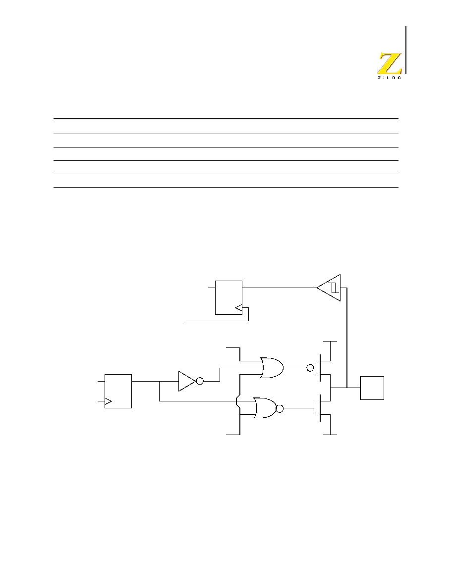
PS019915-1005
General-Purpose
I/O
Z8 Encore!
�
64K Series
Product Specification
52
Architecture
Figure 10 illustrates a simplified block diagram of a GPIO port pin. In this figure, the abil-
ity to accommodate alternate functions and variable port current drive strength are not
illustrated.
Figure 10. GPIO Port Pin Block Diagram
GPIO Alternate Functions
Many of the GPIO port pins can be used as both general-purpose I/O and to provide access
to on-chip peripheral functions such as the timers and serial communication devices. The
Port A�H Alternate Function sub-registers configure these pins for either general-purpose
Z8X6421
40-pin
[7:0]
[7:0]
[6:0]
[6:3, 1:0]
-
-
-
-
Z8X6421
44-pin
[7:0]
[7:0]
[7:0]
[6:0]
-
-
-
-
Z8X6422
64- and 68-pin
[7:0]
[7:0]
[7:0]
[7:0]
[7:0]
[7]
[3]
[3:0]
Z8X6423
80-pin
[7:0]
[7:0]
[7:0]
[7:0]
[7:0]
[7:0]
[7:0]
[3:0]
Table 11. Port Availability by Device and Package Type (Continued)
Device
Packages
Port A
Port B
Port C
Port D
Port E
Port F
Port G
Port H
D
Q
D
Q
GND
VDD
Port Output Control
Port Data Direction
Port Output
Data Register
Port Input
Data Register
Port
Pin
DATA
Bus
System
Clock
System
Clock
Schmitt Trigger

PS019915-1005
General-Purpose
I/O
Z8 Encore!
�
64K Series
Product Specification
53
I/O or alternate function operation. When a pin is configured for alternate function, control
of the port pin direction (input/output) is passed from the Port A�H Data Direction regis-
ters to the alternate function assigned to this pin. Table 12 lists the alternate functions
associated with each port pin.
Table 12. Port Alternate Function Mapping
Port
Pin
Mnemonic
Alternate Function Description
Port A
PA0
T0IN
Timer 0 Input
PA1
T0OUT
Timer 0 Output
PA2
DE0
UART 0 Driver Enable
PA3
CTS0
UART 0 Clear to Send
PA4
RXD0 / IRRX0 UART 0 / IrDA 0 Receive Data
PA5
TXD0 / IRTX0
UART 0 / IrDA 0 Transmit Data
PA6
SCL
I
2
C Clock (automatically open-drain)
PA7
SDA
I
2
C Data (automatically open-drain)
Port B
PB0
ANA0
ADC Analog Input 0
PB1
ANA1
ADC Analog Input 1
PB2
ANA2
ADC Analog Input 2
PB3
ANA3
ADC Analog Input 3
PB4
ANA4
ADC Analog Input 4
PB5
ANA5
ADC Analog Input 5
PB6
ANA6
ADC Analog Input 6
PB7
ANA7
ADC Analog Input 7
Port C
PC0
T1IN
Timer 1 Input
PC1
T1OUT
Timer 1 Output
PC2
SS
SPI Slave Select
PC3
SCK
SPI Serial Clock
PC4
MOSI
SPI Master Out Slave In
PC5
MISO
SPI Master In Slave Out
PC6
T2IN
Timer 2 In
PC7
T2OUT
Timer 2 Out

PS019915-1005
General-Purpose
I/O
Z8 Encore!
�
64K Series
Product Specification
54
GPIO Interrupts
Many of the GPIO port pins can be used as interrupt sources. Some port pins may be con-
figured to generate an interrupt request on either the rising edge or falling edge of the pin
input signal. Other port pin interrupts generate an interrupt when any edge occurs (both
rising and falling). Refer to the Interrupt Controller chapter for more information on
interrupts using the GPIO pins.
GPIO Control Register Definitions
Four registers for each Port provide access to GPIO control, input data, and output data.
Table 13 lists these Port registers. Use the Port A�H Address and Control registers
together to provide access to sub-registers for Port configuration and control.
Port D
PD0
T3IN
Timer 3 In (unavailable in 44-pin packages)
PD1
T3OUT
Timer 3 Out (unavailable in 44-pin packages)
PD2
N/A
No alternate function
PD3
DE1
UART 1 Driver Enable
PD4
RXD1 / IRRX1 UART 1 / IrDA 1 Receive Data
PD5
TXD1 / IRTX1
UART 1 / IrDA 1 Transmit Data
PD6
CTS1
UART 1 Clear to Send
PD7
RCOUT
Watch-Dog Timer RC Oscillator Output
Port E
PE[7:0] N/A
No alternate functions
Port F
PF[7:0] N/A
No alternate functions
Port G
PG[7:0] N/A
No alternate functions
Port H
PH0
ANA8
ADC Analog Input 8
PH1
ANA9
ADC Analog Input 9
PH2
ANA10
ADC Analog Input 10
PH3
ANA11
ADC Analog Input 11
Table 12. Port Alternate Function Mapping (Continued)
Port
Pin
Mnemonic
Alternate Function Description
PS019915-1005
General-Purpose
I/O
Z8 Encore!
�
64K Series
Product Specification
55
Port A-H Address Registers
The Port A�H Address registers select the GPIO Port functionality accessible through the
Port A�H Control registers. The Port A�H Address and Control registers combine to pro-
vide access to all GPIO Port control (Table 14).
Table 13. GPIO Port Registers and Sub-Registers
Port Register Mnemonic
Port Register Name
PxADDR
Port A-H Address Register
(Selects sub-registers)
PxCTL
Port A-H Control Register
(Provides access to sub-registers)
PxIN
Port A-H Input Data Register
PxOUT
Port A-H Output Data Register
Port Sub-Register Mnemonic
Port Register Name
PxDD
Data Direction
PxAF
Alternate Function
PxOC
Output Control (Open-Drain)
PxDD
High Drive Enable
PxSMRE
STOP Mode Recovery Source Enable
Table 14. Port A-H GPIO Address Registers (PxADDR)
BITS
7
6
5
4
3
2
1
0
FIELD
PADDR[7:0]
RESET
00H
R/W
R/W
ADDR
FD0H, FD4H, FD8H, FDCH, FE0H, FE4H, FE8H, FECH
PS019915-1005
General-Purpose
I/O
Z8 Encore!
�
64K Series
Product Specification
56
PADDR[7:0]--Port Address
The Port Address selects one of the sub-registers accessible through the Port Control reg-
ister.
Port A-H Control Registers
The Port A�H Control registers set the GPIO port operation. The value in the correspond-
ing Port A�H Address register determines the control sub-registers accessible using the
Port A�H Control register (Table 15).
PCTL[7:0]--Port Control
The Port Control register provides access to all sub-registers that configure the GPIO Port
operation.
PADDR[7:0] Port Control sub-register accessible using the Port A-H Control Registers
00H
No function. Provides some protection against accidental Port reconfiguration.
01H
Data Direction
02H
Alternate Function
03H
Output Control (Open-Drain)
04H
High Drive Enable
05H
STOP Mode Recovery Source Enable.
06H-FFH
No function.
Table 15. Port A
�
H Control Registers (PxCTL)
BITS
7
6
5
4
3
2
1
0
FIELD
PCTL
RESET
00H
R/W
R/W
ADDR
FD1H, FD5H, FD9H, FDDH, FE1H, FE5H, FE9H, FEDH
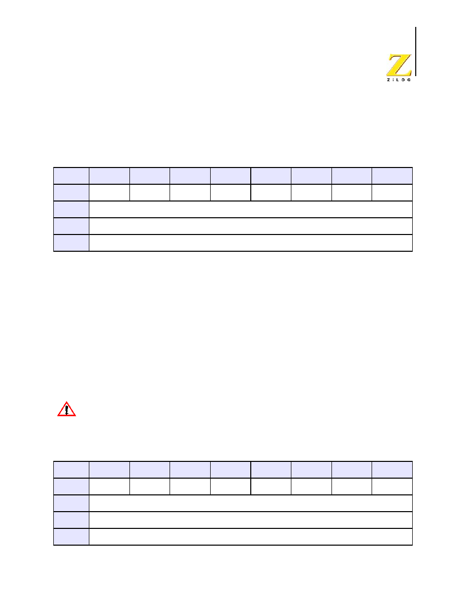
PS019915-1005
General-Purpose
I/O
Z8 Encore!
�
64K Series
Product Specification
57
Port A-H Data Direction Sub-Registers
The Port A�H Data Direction sub-register is accessed through the Port A�H Control regis-
ter by writing 01H to the Port A�H Address register (Table 16).
DD[7:0]--Data Direction
These bits control the direction of the associated port pin. Port Alternate Function opera-
tion overrides the Data Direction register setting.
0 = Output. Data in the Port A�H Output Data register is driven onto the port pin.
1 = Input. The port pin is sampled and the value written into the Port A-H Input Data Reg-
ister. The output driver is tri-stated.
Port A
�
H Alternate Function Sub-Registers
The Port A�H Alternate Function sub-register (Table 17) is accessed through the Port A�
H Control register by writing
02H
to the Port A�H Address register. The Port A�H Alter-
nate Function sub-registers select the alternate functions for the selected pins. Refer to the
GPIO Alternate Functions section to determine the alternate function associated with
each port pin.
Do not enable alternate function for GPIO port pins which do not have an
associated alternate function. Failure to follow this guideline may result in
unpredictable operation.
Table 16. Port A-H Data Direction Sub-Registers
BITS
7
6
5
4
3
2
1
0
FIELD
DD7
DD6
DD5
DD4
DD3
DD2
DD1
DD0
RESET
1
R/W
R/W
ADDR
If 01H in Port A-H Address Register, accessible through Port A-H Control Register
Table 17. Port A-H Alternate Function Sub-Registers
BITS
7
6
5
4
3
2
1
0
FIELD
AF7
AF6
AF5
AF4
AF3
AF2
AF1
AF0
RESET
0
R/W
R/W
ADDR
If 02H in Port A-H Address Register, accessible through Port A-H Control Register
Caution:
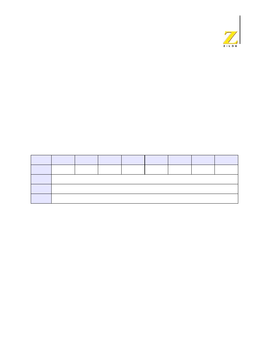
PS019915-1005
General-Purpose
I/O
Z8 Encore!
�
64K Series
Product Specification
58
AF[7:0]--Port Alternate Function enabled
0 = The port pin is in normal mode and the DDx bit in the Port A�H Data Direction sub-
register determines the direction of the pin.
1 = The alternate function is selected. Port pin operation is controlled by the alternate
function.
Port A-H Output Control Sub-Registers
The Port A-H Output Control sub-register (Table 18) is accessed through the Port A�H
Control register by writing
03H
to the Port A�H Address register. Setting the bits in the
Port A�H Output Control sub-registers to 1 configures the specified port pins for open-
drain operation. These sub-registers affect the pins directly and, as a result, alternate func-
tions are also affected.
POC[7:0]--Port Output Control
These bits function independently of the alternate function bit and disables the drains if set
to 1.
0 = The drains are enabled for any output mode.
1 = The drain of the associated pin is disabled (open-drain mode).
Table 18. Port A-H Output Control Sub-Registers
BITS
7
6
5
4
3
2
1
0
FIELD
POC7
POC6
POC5
POC4
POC3
POC2
POC1
POC0
RESET
0
R/W
R/W
ADDR
If 03H in Port A-H Address Register, accessible through Port A-H Control Register
PS019915-1005
General-Purpose
I/O
Z8 Encore!
�
64K Series
Product Specification
59
Port A-H High Drive Enable Sub-Registers
The Port A�H High Drive Enable sub-register (Table 19) is accessed through the Port A�
H Control register by writing
04H
to the Port A-H Address register. Setting the bits in the
Port A�H High Drive Enable sub-registers to 1 configures the specified port pins for high
current output drive operation. The Port A�H High Drive Enable sub-register affects the
pins directly and, as a result, alternate functions are also affected.
PHDE[7:0]--Port High Drive Enabled
0 = The Port pin is configured for standard output current drive.
1 = The Port pin is configured for high output current drive.
Port A-H STOP Mode Recovery Source Enable Sub-Registers
The Port A�H STOP Mode Recovery Source Enable sub-register (Table 20) is accessed
through the Port A�H Control register by writing
05H
to the Port A�H Address register.
Setting the bits in the Port A�H STOP Mode Recovery Source Enable sub-registers to 1
configures the specified Port pins as a STOP Mode Recovery source. During STOP Mode,
any logic transition on a Port pin enabled as a STOP Mode Recovery source initiates
STOP Mode Recovery.
Table 19. Port A
�
H High Drive Enable Sub-Registers
BITS
7
6
5
4
3
2
1
0
FIELD
PHDE7
PHDE6
PHDE5
PHDE4
PHDE3
PHDE2
PHDE1
PHDE0
RESET
0
R/W
R/W
ADDR
If 04H in Port A-H Address Register, accessible through Port A-H Control Register
PS019915-1005
General-Purpose
I/O
Z8 Encore!
�
64K Series
Product Specification
60
PSMRE[7:0]--Port STOP Mode Recovery Source Enabled
0 = The Port pin is not configured as a STOP Mode Recovery source. Transitions on this
pin during STOP mode do not initiate STOP Mode Recovery.
1 = The Port pin is configured as a STOP Mode Recovery source. Any logic transition on
this pin during STOP mode initiates STOP Mode Recovery.
Port A-H Input Data Registers
Reading from the Port A�H Input Data registers (Table 21) returns the sampled values
from the corresponding port pins. The Port A�H Input Data registers are Read-only.
PIN[7:0]--Port Input Data
Sampled data from the corresponding port pin input.
0 = Input data is logical 0 (Low).
1 = Input data is logical 1 (High).
Table 20. Port A-H STOP Mode Recovery Source Enable Sub-Registers
BITS
7
6
5
4
3
2
1
0
FIELD
PSMRE7
PSMRE6
PSMRE5
PSMRE4
PSMRE3
PSMRE2
PSMRE1
PSMRE0
RESET
0
R/W
R/W
ADDR
If 05H in Port A
�
H Address Register, accessible through Port A-H Control Register
Table 21. Port A
�
H Input Data Registers (PxIN)
BITS
7
6
5
4
3
2
1
0
FIELD
PIN7
PIN6
PIN5
PIN4
PIN3
PIN2
PIN1
PIN0
RESET
X
R/W
R
ADDR
FD2H, FD6H, FDAH, FDEH, FE2H, FE6H, FEAH, FEEH
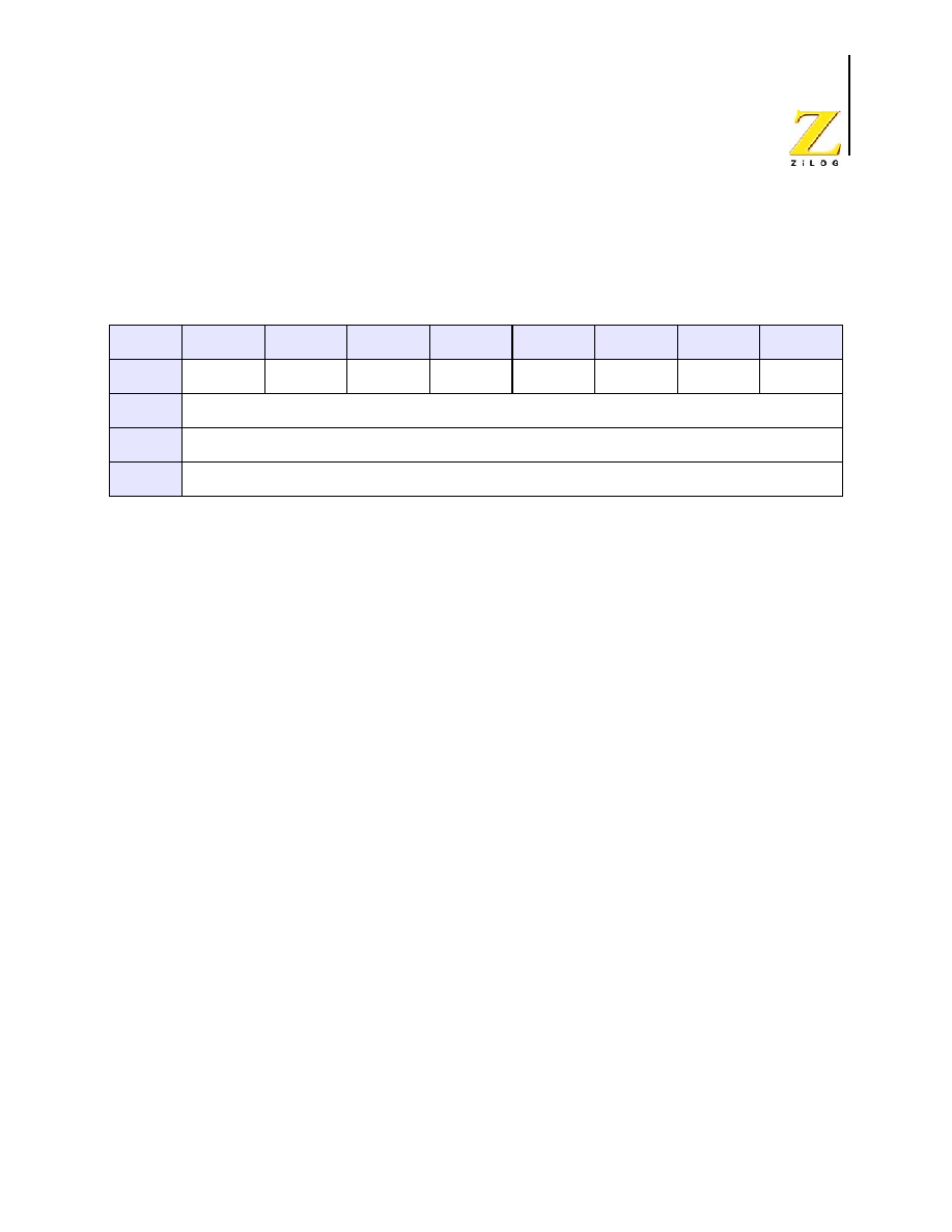
PS019915-1005
General-Purpose
I/O
Z8 Encore!
�
64K Series
Product Specification
61
Port A�H Output Data Register
The Port A�H Output Data register (Table 22) writes output data to the pins.
POUT[7:0]--Port Output Data
These bits contain the data to be driven out from the port pins. The values are only driven
if the corresponding pin is configured as an output and the pin is not configured for alter-
nate function operation.
0 = Drive a logical 0 (Low).
1= Drive a logical 1 (High). High value is not driven if the drain has been disabled by set-
ting the corresponding Port Output Control register bit to 1.
Table 22. Port A-H Output Data Register (PxOUT)
BITS
7
6
5
4
3
2
1
0
FIELD
POUT7
POUT6
POUT5
POUT4
POUT3
POUT2
POUT1
POUT0
RESET
0
R/W
R/W
ADDR
FD3H, FD7H, FDBH, FDFH, FE3H, FE7H, FEBH, FEFH

Z8 Encore!
�
64K Series
Product Specification
PS019915-1005
Interrupt
Controller
62
Interrupt Controller
Overview
The interrupt controller on the 64K Series products prioritizes the interrupt requests from
the on-chip peripherals and the GPIO port pins. The features of the interrupt controller
include the following:
�
24 unique interrupt vectors:
�
12 GPIO port pin interrupt sources
�
12 on-chip peripheral interrupt sources
�
Flexible GPIO interrupts
�
8 selectable rising and falling edge GPIO interrupts
�
4 dual-edge interrupts
�
3 levels of individually programmable interrupt priority
�
Watch-Dog Timer can be configured to generate an interrupt
Interrupt requests (IRQs) allow peripheral devices to suspend CPU operation in an orderly
manner and force the CPU to start an interrupt service routine (ISR). Usually this interrupt
service routine is involved with the exchange of data, status information, or control infor-
mation between the CPU and the interrupting peripheral. When the service routine is com-
pleted, the CPU returns to the operation from which it was interrupted.
The eZ8 CPU supports both vectored and polled interrupt handling. For polled interrupts,
the interrupt control has no effect on operation. Refer to the eZ8 CPU User Manual for
more information regarding interrupt servicing by the eZ8 CPU. The eZ8 CPU User Man-
ual is available for download at
www.zilog.com
.
Interrupt Vector Listing
Table 23 lists all of the interrupts available in order of priority. The interrupt vector is
stored with the most significant byte (MSB) at the even Program Memory address and the
least significant byte (LSB) at the following odd Program Memory address.

PS019915-1005
Interrupt
Controller
Z8 Encore!
�
64K Series
Product Specification
63
Table 23. Interrupt Vectors in Order of Priority
Priority
Program Memory
Vector Address
Interrupt Source
Highest
0002H
Reset (not an interrupt)
0004H
Watch-Dog Timer (see Watch-Dog Timer chapter)
0006H
Illegal Instruction Trap (not an interrupt)
0008H
Timer 2
000AH
Timer 1
000CH
Timer 0
000EH
UART 0 receiver
0010H
UART 0 transmitter
0012H
I
2
C
0014H
SPI
0016H
ADC
0018H
Port A7 or Port D7, rising or falling input edge
001AH
Port A6 or Port D6, rising or falling input edge
001CH
Port A5 or Port D5, rising or falling input edge
001EH
Port A4 or Port D4, rising or falling input edge
0020H
Port A3 or Port D3, rising or falling input edge
0022H
Port A2 or Port D2, rising or falling input edge
0024H
Port A1 or Port D1, rising or falling input edge
0026H
Port A0 or Port D0, rising or falling input edge
0028H
Timer 3 (not available in 44-pin packages)
002AH
UART 1 receiver
002CH
UART 1 transmitter
002EH
DMA
0030H
Port C3, both input edges
0032H
Port C2, both input edges
0034H
Port C1, both input edges
Lowest
0036H
Port C0, both input edges
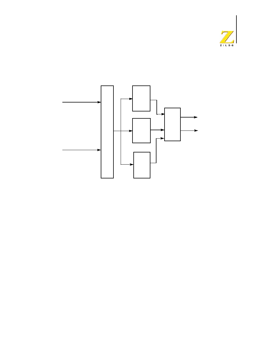
PS019915-1005
Interrupt
Controller
Z8 Encore!
�
64K Series
Product Specification
64
Architecture
Figure 11 illustrates a block diagram of the interrupt controller.
Figure 11. Interrupt Controller Block Diagram
Operation
Master Interrupt Enable
The master interrupt enable bit (IRQE) in the Interrupt Control register globally enables
and disables interrupts.
Interrupts are globally enabled by any of the following actions:
�
Executing an EI (Enable Interrupt) instruction
�
Executing an IRET (Return from Interrupt) instruction
�
Writing a 1 to the IRQE bit in the Interrupt Control register
Interrupts are globally disabled by any of the following actions:
�
Execution of a DI (Disable Interrupt) instruction
�
eZ8 CPU acknowledgement of an interrupt service request from the interrupt
controller
�
Writing a 0 to the IRQE bit in the Interrupt Control register
�
Reset
Vector
IRQ Request
High
Priority
Medium
Priority
Low
Priority
Priority
Mux
Interrupt
Req
uest L
a
tch
e
s a
nd
Con
t
ro
l
Port Interrupts
Internal Interrupts

PS019915-1005
Interrupt
Controller
Z8 Encore!
�
64K Series
Product Specification
65
�
Executing a Trap instruction
�
Illegal Instruction trap
Interrupt Vectors and Priority
The interrupt controller supports three levels of interrupt priority. Level 3 is the highest
priority, Level 2 is the second highest priority, and Level 1 is the lowest priority. If all of
the interrupts were enabled with identical interrupt priority (all as Level 2 interrupts, for
example), then interrupt priority would be assigned from highest to lowest as specified in
Table 23. Level 3 interrupts always have higher priority than Level 2 interrupts which, in
turn, always have higher priority than Level 1 interrupts. Within each interrupt priority
level (Level 1, Level 2, or Level 3), priority is assigned as specified in Table 23. Reset,
Watch-Dog Timer interrupt (if enabled), and Illegal Instruction Trap always have highest
priority.
Interrupt Assertion
Interrupt sources assert their interrupt requests for only a single system clock period (sin-
gle pulse). When the interrupt request is acknowledged by the eZ8 CPU, the correspond-
ing bit in the Interrupt Request register is cleared until the next interrupt occurs. Writing a
0 to the corresponding bit in the Interrupt Request register likewise clears the interrupt
request.
The following style of coding to clear bits in the Interrupt Request registers
is NOT recommended. All incoming interrupts that are received between
execution of the first LDX command and the last LDX command are lost.
Poor coding style that can result in lost interrupt requests:
LDX r0, IRQ0
AND r0, MASK
LDX IRQ0, r0
To avoid missing interrupts, the following style of coding to clear bits in
the Interrupt Request 0 register is recommended:
Good coding style that avoids lost interrupt requests:
ANDX IRQ0, MASK
Software Interrupt Assertion
Program code can generate interrupts directly. Writing a 1 to the desired bit in the Interrupt
Request register triggers an interrupt (assuming that interrupt is enabled). When the inter-
rupt request is acknowledged by the eZ8 CPU, the bit in the Interrupt Request register is
automatically cleared to 0.
Caution:
PS019915-1005
Interrupt
Controller
Z8 Encore!
�
64K Series
Product Specification
66
The following style of coding to generate software interrupts by setting
bits in the Interrupt Request registers is NOT recommended. All incoming
interrupts that are received between execution of the first LDX command
and the last LDX command are lost.
Poor coding style that can result in lost interrupt requests:
LDX r0, IRQ0
OR r0, MASK
LDX IRQ0, r0
To avoid missing interrupts, the following style of coding to set bits in the
Interrupt Request registers is recommended:
Good coding style that avoids lost interrupt requests:
ORX IRQ0, MASK
Interrupt Control Register Definitions
For all interrupts other than the Watch-Dog Timer interrupt, the interrupt control registers
enable individual interrupts, set interrupt priorities, and indicate interrupt requests.
Interrupt Request 0 Register
The Interrupt Request 0 (IRQ0) register (Table 24) stores the interrupt requests for both
vectored and polled interrupts. When a request is presented to the interrupt controller, the
corresponding bit in the IRQ0 register becomes 1. If interrupts are globally enabled (vec-
tored interrupts), the interrupt controller passes an interrupt request to the eZ8 CPU. If
interrupts are globally disabled (polled interrupts), the eZ8 CPU can read the Interrupt
Request 0 register to determine if any interrupt requests are pending
Table 24. Interrupt Request 0 Register (IRQ0)
BITS
7
6
5
4
3
2
1
0
FIELD
T2I
T1I
T0I
U0RXI
U0TXI
I2CI
SPII
ADCI
RESET
0
R/W
R/W
ADDR
FC0H
Caution:

PS019915-1005
Interrupt
Controller
Z8 Encore!
�
64K Series
Product Specification
67
T2I--Timer 2 Interrupt Request
0 = No interrupt request is pending for Timer 2.
1 = An interrupt request from Timer 2 is awaiting service.
T1I--Timer 1 Interrupt Request
0 = No interrupt request is pending for Timer 1.
1 = An interrupt request from Timer 1 is awaiting service.
T0I--Timer 0 Interrupt Request
0 = No interrupt request is pending for Timer 0.
1 = An interrupt request from Timer 0 is awaiting service.
U0RXI--UART 0 Receiver Interrupt Request
0 = No interrupt request is pending for the UART 0 receiver.
1 = An interrupt request from the UART 0 receiver is awaiting service.
U0TXI--UART 0 Transmitter Interrupt Request
0 = No interrupt request is pending for the UART 0 transmitter.
1 = An interrupt request from the UART 0 transmitter is awaiting service.
I
2
CI-- I
2
C Interrupt Request
0 = No interrupt request is pending for the I
2
C.
1 = An interrupt request from the I
2
C is awaiting service.
SPII--SPI Interrupt Request
0 = No interrupt request is pending for the SPI.
1 = An interrupt request from the SPI is awaiting service.
ADCI--ADC Interrupt Request
0 = No interrupt request is pending for the Analog-to-Digital Converter.
1 = An interrupt request from the Analog-to-Digital Converter is awaiting service.
Interrupt Request 1 Register
The Interrupt Request 1 (IRQ1) register (Table 25) stores interrupt requests for both vec-
tored and polled interrupts. When a request is presented to the interrupt controller, the cor-
responding bit in the IRQ1 register becomes 1. If interrupts are globally enabled (vectored
interrupts), the interrupt controller passes an interrupt request to the eZ8 CPU. If interrupts
are globally disabled (polled interrupts), the eZ8 CPU can read the Interrupt Request 1
register to determine if any interrupt requests are pending.
PS019915-1005
Interrupt
Controller
Z8 Encore!
�
64K Series
Product Specification
68
PADxI--Port A or Port D Pin x Interrupt Request
0 = No interrupt request is pending for GPIO Port A or Port D pin x.
1 = An interrupt request from GPIO Port A or Port D pin x is awaiting service.
where x indicates the specific GPIO Port pin number (0 through 7). For each pin, only 1 of
either Port A or Port D can be enabled for interrupts at any one time. Port selection (A or
D) is determined by the values in the Interrupt Port Select Register.
Interrupt Request 2 Register
The Interrupt Request 2 (IRQ2) register (Table 26) stores interrupt requests for both vec-
tored and polled interrupts. When a request is presented to the interrupt controller, the cor-
responding bit in the IRQ2 register becomes 1. If interrupts are globally enabled (vectored
interrupts), the interrupt controller passes an interrupt request to the eZ8 CPU. If interrupts
are globally disabled (polled interrupts), the eZ8 CPU can read the Interrupt Request 1
register to determine if any interrupt requests are pending.
T3I--Timer 3 Interrupt Request
0 = No interrupt request is pending for Timer 3.
1 = An interrupt request from Timer 3 is awaiting service.
Table 25. Interrupt Request 1 Register (IRQ1)
BITS
7
6
5
4
3
2
1
0
FIELD
PAD7I
PAD6I
PAD5I
PAD4I
PAD3I
PAD2I
PAD1I
PAD0I
RESET
0
R/W
R/W
ADDR
FC3H
Table 26. Interrupt Request 2 Register (IRQ2)
BITS
7
6
5
4
3
2
1
0
FIELD
T3I
U1RXI
U1TXI
DMAI
PC3I
PC2I
PC1I
PC0I
RESET
0
R/W
R/W
ADDR
FC6H
PS019915-1005
Interrupt
Controller
Z8 Encore!
�
64K Series
Product Specification
69
U1RXI--UART 1 Receive Interrupt Request
0 = No interrupt request is pending for the UART1 receiver.
1 = An interrupt request from UART1 receiver is awaiting service.
U1TXI--UART 1 Transmit Interrupt Request
0 = No interrupt request is pending for the UART 1 transmitter.
1 = An interrupt request from the UART 1 transmitter is awaiting service.
DMAI--DMA Interrupt Request
0 = No interrupt request is pending for the DMA.
1 = An interrupt request from the DMA is awaiting service.
PCxI--Port C Pin x Interrupt Request
0 = No interrupt request is pending for GPIO Port C pin x.
1 = An interrupt request from GPIO Port C pin x is awaiting service.
where x indicates the specific GPIO Port C pin number (0 through 3).
IRQ0 Enable High and Low Bit Registers
The IRQ0 Enable High and Low Bit registers (Tables 28 and 29) form a priority encoded
enabling for interrupts in the Interrupt Request 0 register. Priority is generated by setting
bits in each register. Table 27 describes the priority control for IRQ0.
Table 27. IRQ0 Enable and Priority Encoding
IRQ0ENH[x] IRQ0ENL[x] Priority
Description
0
0
Disabled
Disabled
0
1
Level 1
Low
1
0
Level 2
Nominal
1
1
Level 3
High
where x indicates the register bits from 0 through 7.
Table 28. IRQ0 Enable High Bit Register (IRQ0ENH)
BITS
7
6
5
4
3
2
1
0
FIELD
T2ENH
T1ENH
T0ENH
U0RENH
U0TENH
I2CENH
SPIENH
ADCENH
RESET
0
R/W
R/W
ADDR
FC1H
PS019915-1005
Interrupt
Controller
Z8 Encore!
�
64K Series
Product Specification
70
T2ENH--Timer 2 Interrupt Request Enable High Bit
T1ENH--Timer 1 Interrupt Request Enable High Bit
T0ENH--Timer 0 Interrupt Request Enable High Bit
U0RENH--UART 0 Receive Interrupt Request Enable High Bit
U0TENH--UART 0 Transmit Interrupt Request Enable High Bit
I2CENH--I
2
C Interrupt Request Enable High Bit
SPIENH--SPI Interrupt Request Enable High Bit
ADCENH--ADC Interrupt Request Enable High Bit
T2ENL--Timer 2 Interrupt Request Enable Low Bit
T1ENL--Timer 1 Interrupt Request Enable Low Bit
T0ENL--Timer 0 Interrupt Request Enable Low Bit
U0RENL--UART 0 Receive Interrupt Request Enable Low Bit
U0TENL--UART 0 Transmit Interrupt Request Enable Low Bit
I2CENL--I
2
C Interrupt Request Enable Low Bit
SPIENL--SPI Interrupt Request Enable Low Bit
ADCENL--ADC Interrupt Request Enable Low Bit
IRQ1 Enable High and Low Bit Registers
The IRQ1 Enable High and Low Bit registers (Tables 31 and 32) form a priority encoded
enabling for interrupts in the Interrupt Request 1 register. Priority is generated by setting
bits in each register. Table 30 describes the priority control for IRQ1.
Table 29. IRQ0 Enable Low Bit Register (IRQ0ENL)
BITS
7
6
5
4
3
2
1
0
FIELD
T2ENL
T1ENL
T0ENL
U0RENL
U0TENL
I2CENL
SPIENL
ADCENL
RESET
0
R/W
R/W
ADDR
FC2H
Table 30. IRQ1 Enable and Priority Encoding
IRQ1ENH[x] IRQ1ENL[x] Priority
Description
0
0
Disabled
Disabled
0
1
Level 1
Low
1
0
Level 2
Nominal
1
1
Level 3
High
where x indicates the register bits from 0 through 7.
PS019915-1005
Interrupt
Controller
Z8 Encore!
�
64K Series
Product Specification
71
PADxENH--Port A or Port D Bit[x] Interrupt Request Enable High Bit
Refer to the Interrupt Port Select register for selection of either Port A or Port D as the
interrupt source.
PADxENL--Port A or Port D Bit[x] Interrupt Request Enable Low Bit
Refer to the Interrupt Port Select register for selection of either Port A or Port D as the
interrupt source.
IRQ2 Enable High and Low Bit Registers
The IRQ2 Enable High and Low Bit registers (Tables 34 and 35) form a priority encoded
enabling for interrupts in the Interrupt Request 2 register. Priority is generated by setting
bits in each register. Table 33 describes the priority control for IRQ2.
Table 31. IRQ1 Enable High Bit Register (IRQ1ENH)
BITS
7
6
5
4
3
2
1
0
FIELD
PAD7ENH PAD6ENH PAD5ENH PAD4ENH PAD3ENH PAD2ENH PAD1ENH PAD0ENH
RESET
0
0
0
0
0
0
0
0
R/W
R/W
R/W
R/W
R/W
R/W
R/W
R/W
R/W
ADDR
FC4H
Table 32. IRQ1 Enable Low Bit Register (IRQ1ENL)
BITS
7
6
5
4
3
2
1
0
FIELD
PAD7ENL PAD6ENL PAD5ENL PAD4ENL PAD3ENL PAD2ENL PAD1ENL PAD0ENL
RESET
0
0
0
0
0
0
0
0
R/W
R/W
R/W
R/W
R/W
R/W
R/W
R/W
R/W
ADDR
FC5H
Table 33. IRQ2 Enable and Priority Encoding
IRQ2ENH[x] IRQ2ENL[x] Priority
Description
0
0
Disabled
Disabled
0
1
Level 1
Low
1
0
Level 2
Nominal
1
1
Level 3
High
where x indicates the register bits from 0 through 7.
PS019915-1005
Interrupt
Controller
Z8 Encore!
�
64K Series
Product Specification
72
T3ENH--Timer 3 Interrupt Request Enable High Bit
U1RENH--UART 1 Receive Interrupt Request Enable High Bit
U1TENH--UART 1 Transmit Interrupt Request Enable High Bit
DMAENH--DMA Interrupt Request Enable High Bit
C3ENH--Port C3 Interrupt Request Enable High Bit
C2ENH--Port C2 Interrupt Request Enable High Bit
C1ENH--Port C1 Interrupt Request Enable High Bit
C0ENH--Port C0 Interrupt Request Enable High Bit
T3ENL--Timer 3 Interrupt Request Enable Low Bit
U1RENL--UART 1 Receive Interrupt Request Enable Low Bit
U1TENL--UART 1 Transmit Interrupt Request Enable Low Bit
DMAENL--DMA Interrupt Request Enable Low Bit
C3ENL--Port C3 Interrupt Request Enable Low Bit
C2ENL--Port C2 Interrupt Request Enable Low Bit
C1ENL--Port C1 Interrupt Request Enable Low Bit
C0ENL--Port C0 Interrupt Request Enable Low Bit
Interrupt Edge Select Register
The Interrupt Edge Select (IRQES) register (Table 36) determines whether an interrupt is
generated for the rising edge or falling edge on the selected GPIO Port input pin. The
Table 34. IRQ2 Enable High Bit Register (IRQ2ENH)
BITS
7
6
5
4
3
2
1
0
FIELD
T3ENH
U1RENH
U1TENH
DMAENH
C3ENH
C2ENH
C1ENH
C0ENH
RESET
0
R/W
R/W
ADDR
FC7H
Table 35. IRQ2 Enable Low Bit Register (IRQ2ENL)
BITS
7
6
5
4
3
2
1
0
FIELD
T3ENL
U1RENL
U1TENL
DMAENL
C3ENL
C2ENL
C1ENL
C0ENL
RESET
0
R/W
R/W
ADDR
FC8H
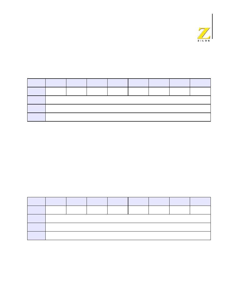
PS019915-1005
Interrupt
Controller
Z8 Encore!
�
64K Series
Product Specification
73
Interrupt Port Select register selects between Port A and Port D for the individual inter-
rupts.
IESx--Interrupt Edge Select x
The minimum pulse width should be greater than 1 system clock to guarantee capture of
the edge triggered interrupt. Shorter pulses may be captured but not guaranteed.
0 = An interrupt request is generated on the falling edge of the PAx/PDx input.
1 = An interrupt request is generated on the rising edge of the PAx/PDx input.
where x indicates the specific GPIO Port pin number (0 through 7),
Interrupt Port Select Register
The Port Select (IRQPS) register (Table 37) determines the port pin that generates the
PAx/PDx interrupts. This register allows either Port A or Port D pins to be used as inter-
rupts. The Interrupt Edge Select register controls the active interrupt edge.
PADxS--PAx/PDx Selection
0 = PAx is used for the interrupt for PAx/PDx interrupt request.
1 = PDx is used for the interrupt for PAx/PDx interrupt request.
where x indicates the specific GPIO Port pin number (0 through 7)
Table 36. Interrupt Edge Select Register (IRQES)
BITS
7
6
5
4
3
2
1
0
FIELD
IES7
IES6
IES5
IES4
IES3
IES2
IES1
IES0
RESET
0
R/W
R/W
ADDR
FCDH
Table 37. Interrupt Port Select Register (IRQPS)
BITS
7
6
5
4
3
2
1
0
FIELD
PAD7S
PAD6S
PAD5S
PAD4S
PAD3S
PAD2S
PAD1S
PAD0S
RESET
0
R/W
R/W
ADDR
FCEH
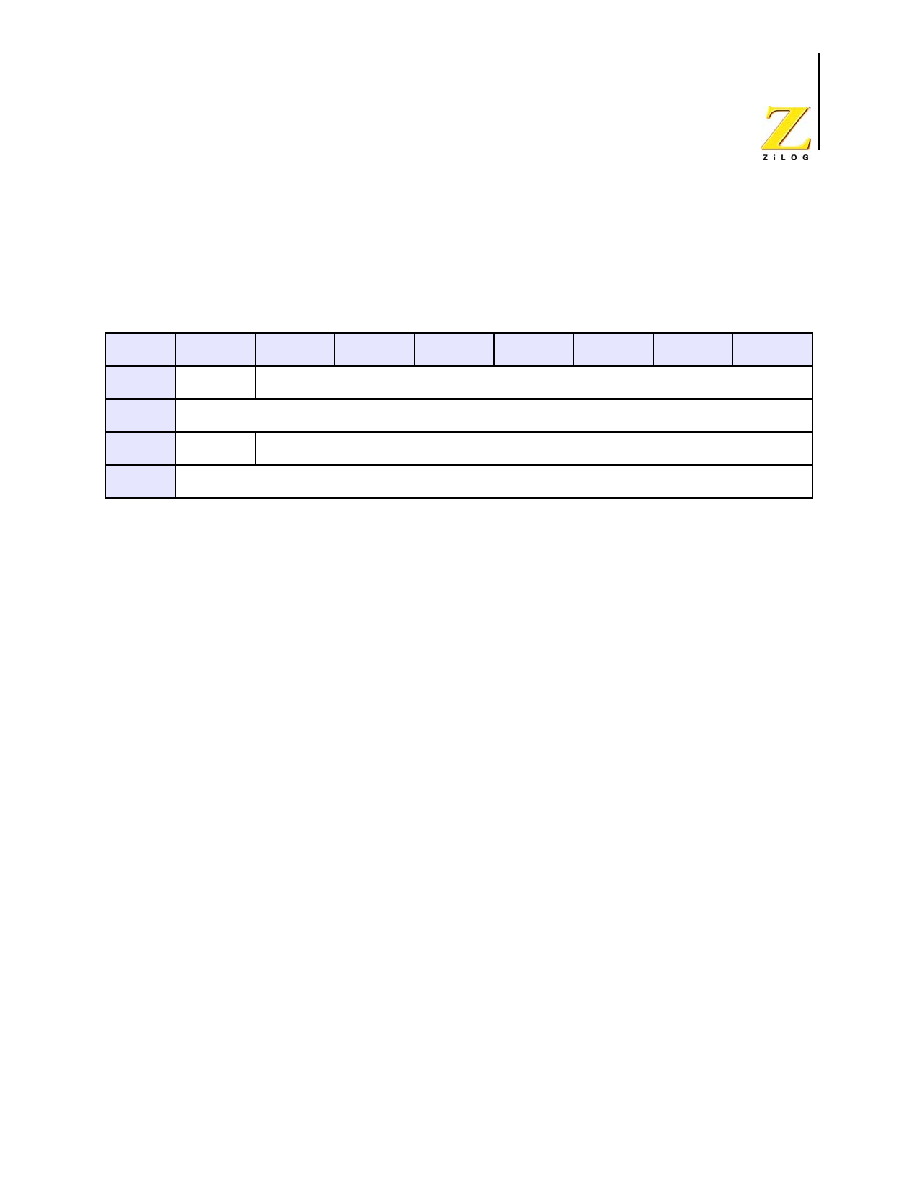
PS019915-1005
Interrupt
Controller
Z8 Encore!
�
64K Series
Product Specification
74
Interrupt Control Register
The Interrupt Control (IRQCTL) register (Table 38) contains the master enable bit for all
interrupts.
IRQE--Interrupt Request Enable
This bit is set to 1 by execution of an EI (Enable Interrupts) or IRET (Interrupt Return)
instruction, or by a direct register write of a 1 to this bit. It is reset to 0 by executing a DI
instruction, eZ8 CPU acknowledgement of an interrupt request, or Reset.
0 = Interrupts are disabled
1 = Interrupts are enabled
Reserved
Must be 0.
Table 38. Interrupt Control Register (IRQCTL)
BITS
7
6
5
4
3
2
1
0
FIELD
IRQE
Reserved
RESET
0
R/W
R/W
R
ADDR
FCFH

Z8 Encore!
�
64K Series
Product Specification
PS019915-1005
Timers
75
Timers
Overview
The 64K Series products contain up to four 16-bit reloadable timers that can be used for
timing, event counting, or generation of pulse-width modulated (PWM) signals. The tim-
ers' features include:
�
16-bit reload counter
�
Programmable prescaler with prescale values from 1 to 128
�
PWM output generation
�
Capture and compare capability
�
External input pin for timer input, clock gating, or capture signal. External input pin
signal frequency is limited to a maximum of one-fourth the system clock frequency.
�
Timer output pin
�
Timer interrupt
In addition to the timers described in this chapter, the Baud Rate Generators for any
unused UART, SPI, or I
2
C peripherals may also be used to provide basic timing function-
ality. Refer to the respective serial communication peripheral chapters for information on
using the Baud Rate Generators as timers. Timer 3 is unavailable in the 44-pin package
devices.
Architecture
Figure 12 illustrates the architecture of the timers.
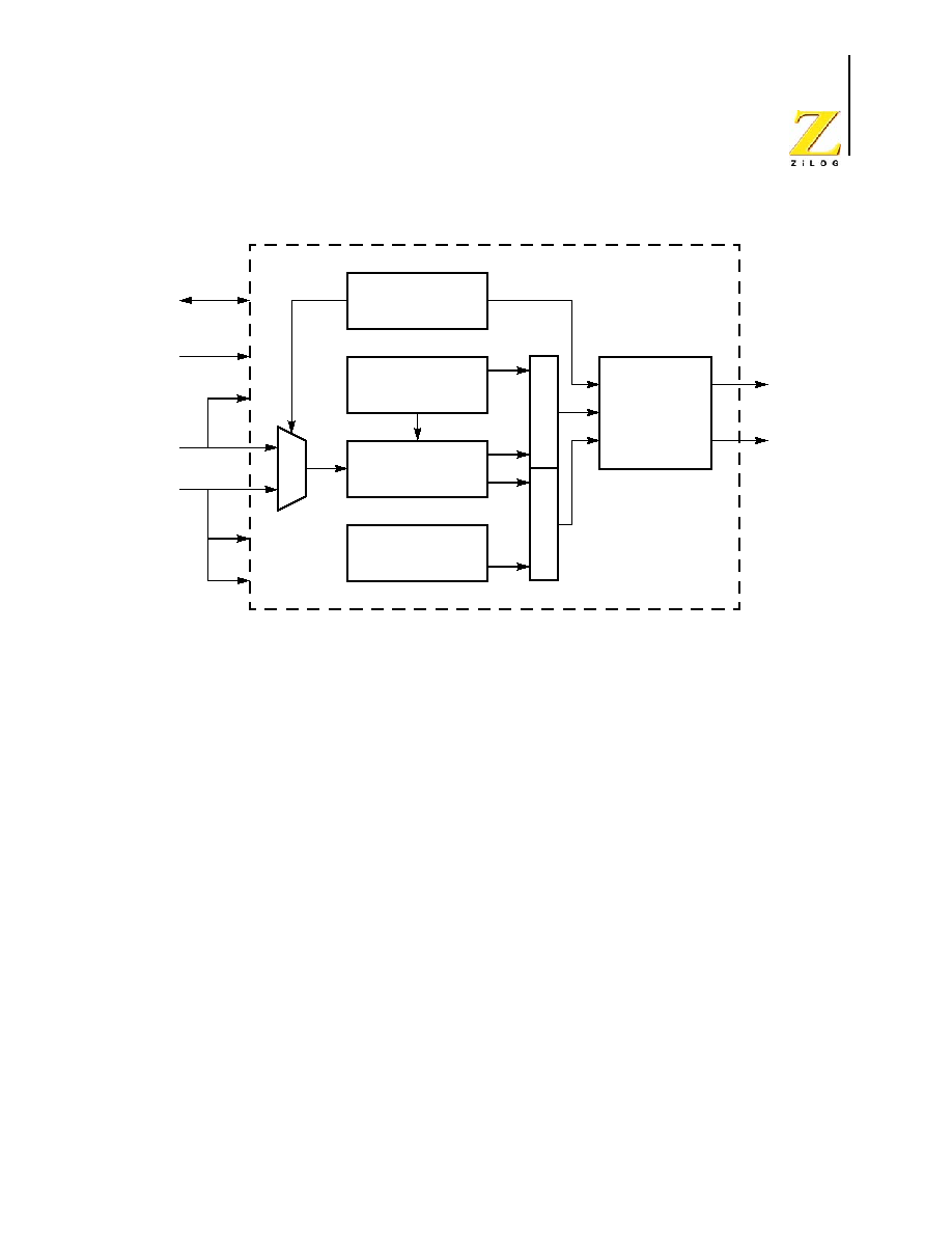
PS019915-1005
Timers
Z8 Encore!
�
64K Series
Product Specification
76
Figure 12. Timer Block Diagram
Operation
The timers are 16-bit up-counters. Minimum time-out delay is set by loading the value
0001H
into the Timer Reload High and Low Byte registers and setting the prescale value
to 1. Maximum time-out delay is set by loading the value
0000H
into the Timer Reload
High and Low Byte registers and setting the prescale value to 128. If the Timer reaches
FFFFH
, the timer rolls over to
0000H
and continues counting.
Timer Operating Modes
The timers can be configured to operate in the following modes:
ONE-SHOT Mode
In ONE-SHOT mode, the timer counts up to the 16-bit Reload value stored in the Timer
Reload High and Low Byte registers. The timer input is the system clock. Upon reaching
the Reload value, the timer generates an interrupt and the count value in the Timer High
and Low Byte registers is reset to
0001H
. Then, the timer is automatically disabled and
stops counting.
Also, if the Timer Output alternate function is enabled, the Timer Output pin changes state
for one system clock cycle (from Low to High or from High to Low) upon timer Reload. If
it is desired to have the Timer Output make a permanent state change upon One-Shot time-
16-Bit
PWM / Compare
16-Bit Counter
with Prescaler
16-Bit
Reload Register
Timer
Control
C
o
mpare
C
o
mpare
Interrupt,
PWM,
and
Timer Output
Control
Timer
Timer
Timer Block
System
Timer
Data
Block
Interrupt
Output
Control
Bus
Clock
Input
Gate
Input
Capture
Input

PS019915-1005
Timers
Z8 Encore!
�
64K Series
Product Specification
77
out, first set the TPOL bit in the Timer Control 1 Register to the start value before begin-
ning ONE-SHOT mode. Then, after starting the timer, set TPOL to the opposite bit value.
The steps for configuring a timer for ONE-SHOT mode and initiating the count are as fol-
lows:
1. Write to the Timer Control 1 register to:
�
Disable the timer
�
Configure the timer for ONE-SHOT mode
�
Set the prescale value
�
If using the Timer Output alternate function, set the initial output level (High or
Low)
2. Write to the Timer High and Low Byte registers to set the starting count value
3. Write to the Timer Reload High and Low Byte registers to set the Reload value
4. If desired, enable the timer interrupt and set the timer interrupt priority by writing to
the relevant interrupt registers
5. If using the Timer Output function, configure the associated GPIO port pin for the
Timer Output alternate function
6. Write to the Timer Control 1 register to enable the timer and initiate counting
In ONE-SHOT mode, the system clock always provides the timer input. The timer period
is given by the following equation:
CONTINUOUS Mode
In CONTINUOUS mode, the timer counts up to the 16-bit Reload value stored in the
Timer Reload High and Low Byte registers. The timer input is the system clock. Upon
reaching the Reload value, the timer generates an interrupt, the count value in the Timer
High and Low Byte registers is reset to
0001H
and counting resumes. Also, if the Timer
Output alternate function is enabled, the Timer Output pin changes state (from Low to
High or from High to Low) upon timer Reload.
The steps for configuring a timer for CONTINUOUS mode and initiating the count are as
follows:
1. Write to the Timer Control 1 register to:
�
Disable the timer
�
Configure the timer for CONTINUOUS mode
�
Set the prescale value
One-Shot Mode Time-Out Period (s)
Reload Value
Start Value
(
) Prescale
�
System Clock Frequency (Hz)
--------------------------------------------------------------------------------------------------------
=

PS019915-1005
Timers
Z8 Encore!
�
64K Series
Product Specification
78
�
If using the Timer Output alternate function, set the initial output level (High or
Low)
2. Write to the Timer High and Low Byte registers to set the starting count value (usually
0001H
), affecting only the first pass in CONTINUOUS mode. After the first timer
Reload in CONTINUOUS mode, counting always begins at the reset value of
0001H
.
3. Write to the Timer Reload High and Low Byte registers to set the Reload value.
4. If desired, enable the timer interrupt and set the timer interrupt priority by writing to
the relevant interrupt registers.
5. If using the Timer Output function, configure the associated GPIO port pin for the
Timer Output alternate function.
6. Write to the Timer Control 1 register to enable the timer and initiate counting.
In CONTINUOUS mode, the system clock always provides the timer input. The timer
period is given by the following equation:
If an initial starting value other than
0001H
is loaded into the Timer High and Low Byte
registers, the ONE-SHOT mode equation must be used to determine the first time-out
period.
COUNTER Mode
In COUNTER mode, the timer counts input transitions from a GPIO port pin. The timer
input is taken from the GPIO Port pin Timer Input alternate function. The TPOL bit in the
Timer Control 1 Register selects whether the count occurs on the rising edge or the falling
edge of the Timer Input signal. In COUNTER mode, the prescaler is disabled.
The input frequency of the Timer Input signal must not exceed one-fourth
the system clock frequency.
Upon reaching the Reload value stored in the Timer Reload High and Low Byte registers,
the timer generates an interrupt, the count value in the Timer High and Low Byte registers
is reset to
0001H
and counting resumes. Also, if the Timer Output alternate function is
enabled, the Timer Output pin changes state (from Low to High or from High to Low) at
timer Reload.
The steps for configuring a timer for COUNTER mode and initiating the count are as fol-
lows:
1. Write to the Timer Control 1 register to:
�
Disable the timer
�
Configure the timer for COUNTER mode
Continuous Mode Time-Out Period (s)
Reload Value Prescale
�
System Clock Frequency (Hz)
----------------------------------------------------------------------------
=
Caution:

PS019915-1005
Timers
Z8 Encore!
�
64K Series
Product Specification
79
�
Select either the rising edge or falling edge of the Timer Input signal for the count.
This also sets the initial logic level (High or Low) for the Timer Output alternate
function. However, the Timer Output function does not have to be enabled
2. Write to the Timer High and Low Byte registers to set the starting count value. This
only affects the first pass in COUNTER mode. After the first timer Reload in
COUNTER mode, counting always begins at the reset value of
0001H
. Generally, in
COUNTER mode the Timer High and Low Byte registers must be written with the
value
0001H
.
3. Write to the Timer Reload High and Low Byte registers to set the Reload value.
4. If desired, enable the timer interrupt and set the timer interrupt priority by writing to
the relevant interrupt registers.
5. Configure the associated GPIO port pin for the Timer Input alternate function.
6. If using the Timer Output function, configure the associated GPIO port pin for the
Timer Output alternate function.
7. Write to the Timer Control 1 register to enable the timer.
In COUNTER mode, the number of Timer Input transitions since the timer start is given
by the following equation:
PWM Mode
In PWM mode, the timer outputs a Pulse-Width Modulator (PWM) output signal through
a GPIO Port pin. The timer input is the system clock. The timer first counts up to the 16-
bit PWM match value stored in the Timer PWM High and Low Byte registers. When the
timer count value matches the PWM value, the Timer Output toggles. The timer continues
counting until it reaches the Reload value stored in the Timer Reload High and Low Byte
registers. Upon reaching the Reload value, the timer generates an interrupt, the count
value in the Timer High and Low Byte registers is reset to
0001H
and counting resumes.
If the TPOL bit in the Timer Control 1 register is set to 1, the Timer Output signal begins
as a High (1) and then transitions to a Low (0) when the timer value matches the PWM
value. The Timer Output signal returns to a High (1) after the timer reaches the Reload
value and is reset to
0001H
.
If the TPOL bit in the Timer Control 1 register is set to 0, the Timer Output signal begins
as a Low (0) and then transitions to a High (1) when the timer value matches the PWM
value. The Timer Output signal returns to a Low (0) after the timer reaches the Reload
value and is reset to
0001H
.
The steps for configuring a timer for PWM mode and initiating the PWM operation are as
follows:
Counter Mode Timer Input Transitions
Current Count Value
Start Value
=

PS019915-1005
Timers
Z8 Encore!
�
64K Series
Product Specification
80
1. Write to the Timer Control 1 register to:
�
Disable the timer
�
Configure the timer for PWM mode
�
Set the prescale value
�
Set the initial logic level (High or Low) and PWM High/Low transition for the
Timer Output alternate function
2. Write to the Timer High and Low Byte registers to set the starting count value
(typically
0001H
). This only affects the first pass in PWM mode. After the first timer
reset in PWM mode, counting always begins at the reset value of
0001H
.
3. Write to the PWM High and Low Byte registers to set the PWM value.
4. Write to the Timer Reload High and Low Byte registers to set the Reload value (PWM
period). The Reload value must be greater than the PWM value.
5. If desired, enable the timer interrupt and set the timer interrupt priority by writing to
the relevant interrupt registers.
6. Configure the associated GPIO port pin for the Timer Output alternate function.
7. Write to the Timer Control 1 register to enable the timer and initiate counting.
The PWM period is given by the following equation:
If an initial starting value other than
0001H
is loaded into the Timer High and Low Byte
registers, the One-Shot mode equation must be used to determine the first PWM time-out
period.
If TPOL is set to 0, the ratio of the PWM output High time to the total period is given by:
If TPOL is set to 1, the ratio of the PWM output High time to the total period is given by:
Capture Mode
In CAPTURE mode, the current timer count value is recorded when the desired external
Timer Input transition occurs. The Capture count value is written to the Timer PWM High
and Low Byte Registers. The timer input is the system clock. The TPOL bit in the Timer
Control 1 register determines if the Capture occurs on a rising edge or a falling edge of the
PWM Period (s)
Reload Value Prescale
�
System Clock Frequency (Hz)
----------------------------------------------------------------------------
=
PWM Output High Time Ratio (%)
Reload Value
PWM Value
Reload Value
-------------------------------------------------------------------------- 100
�
=
PWM Output High Time Ratio (%)
PWM Value
Reload Value
---------------------------------- 100
�
=

PS019915-1005
Timers
Z8 Encore!
�
64K Series
Product Specification
81
Timer Input signal. When the Capture event occurs, an interrupt is generated and the timer
continues counting.
The timer continues counting up to the 16-bit Reload value stored in the Timer Reload
High and Low Byte registers. Upon reaching the Reload value, the timer generates an
interrupt and continues counting.
The steps for configuring a timer for CAPTURE mode and initiating the count are as fol-
lows:
1. Write to the Timer Control 1 register to:
�
Disable the timer
�
Configure the timer for CAPTURE mode.
�
Set the prescale value.
�
Set the Capture edge (rising or falling) for the Timer Input.
2. Write to the Timer High and Low Byte registers to set the starting count value
(typically
0001H
).
3. Write to the Timer Reload High and Low Byte registers to set the Reload value.
4. Clear the Timer PWM High and Low Byte registers to 0000H. This allows user
software to determine if interrupts were generated by either a capture event or a
reload. If the PWM High and Low Byte registers still contain 0000H after the
interrupt, then the interrupt was generated by a Reload.
5. If desired, enable the timer interrupt and set the timer interrupt priority by writing to
the relevant interrupt registers.
6. Configure the associated GPIO port pin for the Timer Input alternate function.
7. Write to the Timer Control 1 register to enable the timer and initiate counting.
In CAPTURE mode, the elapsed time from timer start to Capture event can be calculated
using the following equation:
Compare Mode
In COMPARE mode, the timer counts up to the 16-bit maximum Compare value stored in
the Timer Reload High and Low Byte registers. The timer input is the system clock. Upon
reaching the Compare value, the timer generates an interrupt and counting continues (the
timer value is not reset to
0001H
). Also, if the Timer Output alternate function is enabled,
the Timer Output pin changes state (from Low to High or from High to Low) upon Com-
pare.
Capture Elapsed Time (s)
Capture Value
Start Value
(
) Prescale
�
System Clock Frequency (Hz)
-----------------------------------------------------------------------------------------------------------
=

PS019915-1005
Timers
Z8 Encore!
�
64K Series
Product Specification
82
If the Timer reaches
FFFFH
, the timer rolls over to
0000H
and continue counting.
The steps for configuring a timer for COMPARE mode and initiating the count are as fol-
lows:
1. Write to the Timer Control 1 register to:
�
Disable the timer
�
Configure the timer for COMPARE mode
�
Set the prescale value
�
Set the initial logic level (High or Low) for the Timer Output alternate function, if
desired
2. Write to the Timer High and Low Byte registers to set the starting count value.
3. Write to the Timer Reload High and Low Byte registers to set the Compare value.
4. If desired, enable the timer interrupt and set the timer interrupt priority by writing to
the relevant interrupt registers.
5. If using the Timer Output function, configure the associated GPIO port pin for the
Timer Output alternate function.
6. Write to the Timer Control 1 register to enable the timer and initiate counting.
In COMPARE mode, the system clock always provides the timer input. The Compare time
is given by the following equation:
GATED Mode
In GATED mode, the timer counts only when the Timer Input signal is in its active state
(asserted), as determined by the TPOL bit in the Timer Control 1 register. When the Timer
Input signal is asserted, counting begins. A timer interrupt is generated when the Timer
Input signal is deasserted or a timer reload occurs. To determine if a Timer Input signal
deassertion generated the interrupt, read the associated GPIO input value and compare to
the value stored in the TPOL bit.
The timer counts up to the 16-bit Reload value stored in the Timer Reload High and Low
Byte registers. The timer input is the system clock. When reaching the Reload value, the
timer generates an interrupt, the count value in the Timer High and Low Byte registers is
reset to
0001H
and counting resumes (assuming the Timer Input signal is still asserted).
Also, if the Timer Output alternate function is enabled, the Timer Output pin changes state
(from Low to High or from High to Low) at timer reset.
Compare Mode Time (s)
Compare Value
Start Value
(
) Prescale
�
System Clock Frequency (Hz)
--------------------------------------------------------------------------------------------------------------
=

PS019915-1005
Timers
Z8 Encore!
�
64K Series
Product Specification
83
The steps for configuring a timer for GATED mode and initiating the count are as follows:
1. Write to the Timer Control 1 register to:
�
Disable the timer
�
Configure the timer for GATED mode
�
Set the prescale value
2. Write to the Timer High and Low Byte registers to set the starting count value. This
only affects the first pass in GATED mode. After the first timer reset in GATED mode,
counting always begins at the reset value of
0001H
.
3. Write to the Timer Reload High and Low Byte registers to set the Reload value.
4. If desired, enable the timer interrupt and set the timer interrupt priority by writing to
the relevant interrupt registers.
5. Configure the associated GPIO port pin for the Timer Input alternate function.
6. Write to the Timer Control 1 register to enable the timer.
7. Assert the Timer Input signal to initiate the counting.
CAPTURE/COMPARE Mode
In CAPTURE/COMPARE mode, the timer begins counting on the first external Timer
Input transition. The desired transition (rising edge or falling edge) is set by the TPOL bit
in the Timer Control 1 Register. The timer input is the system clock.
Every subsequent desired transition (after the first) of the Timer Input signal captures the
current count value. The Capture value is written to the Timer PWM High and Low Byte
Registers. When the Capture event occurs, an interrupt is generated, the count value in the
Timer High and Low Byte registers is reset to
0001H
, and counting resumes.
If no Capture event occurs, the timer counts up to the 16-bit Compare value stored in the
Timer Reload High and Low Byte registers. Upon reaching the Compare value, the timer
generates an interrupt, the count value in the Timer High and Low Byte registers is reset to
0001H and counting resumes.
The steps for configuring a timer for CAPTURE/COMPARE mode and initiating the
count are as follows:
1. Write to the Timer Control 1 register to:
�
Disable the timer
�
Configure the timer for CAPTURE/COMPARE mode
�
Set the prescale value
�
Set the Capture edge (rising or falling) for the Timer Input
2. Write to the Timer High and Low Byte registers to set the starting count value
(typically
0001H
).

PS019915-1005
Timers
Z8 Encore!
�
64K Series
Product Specification
84
3. Write to the Timer Reload High and Low Byte registers to set the Compare value.
4. If desired, enable the timer interrupt and set the timer interrupt priority by writing to
the relevant interrupt registers.
5. Configure the associated GPIO port pin for the Timer Input alternate function.
6. Write to the Timer Control 1 register to enable the timer.
7. Counting begins on the first appropriate transition of the Timer Input signal. No
interrupt is generated by this first edge.
In m/COMPARE mode, the elapsed time from timer start to Capture event can be calcu-
lated using the following equation:
Reading the Timer Count Values
The current count value in the timers can be read while counting (enabled). This capability
has no effect on timer operation. When the timer is enabled and the Timer High Byte reg-
ister is read, the contents of the Timer Low Byte register are placed in a holding register. A
subsequent read from the Timer Low Byte register returns the value in the holding register.
This operation allows accurate reads of the full 16-bit timer count value while enabled.
When the timers are not enabled, a read from the Timer Low Byte register returns the
actual value in the counter.
Timer Output Signal Operation
Timer Output is a GPIO Port pin alternate function. Generally, the Timer Output is toggled
every time the counter is reloaded.
Timer Control Register Definitions
Timers 0-2 are available in all packages. Timer 3 is only available in the 64-, 68-, and 80-
pin packages.
Timer 0-3 High and Low Byte Registers
The Timer 0-3 High and Low Byte (TxH and TxL) registers (Tables 38 and 39) contain the
current 16-bit timer count value. When the timer is enabled, a read from TxH causes the
value in TxL to be stored in a temporary holding register. A read from TMRL always
returns this temporary register when the timers are enabled. When the timer is disabled,
reads from the TMRL reads the register directly.
Writing to the Timer High and Low Byte registers while the timer is enabled is not recom-
mended. There are no temporary holding registers available for write operations, so simul-
Capture Elapsed Time (s)
Capture Value
Start Value
(
) Prescale
�
System Clock Frequency (Hz)
-----------------------------------------------------------------------------------------------------------
=
PS019915-1005
Timers
Z8 Encore!
�
64K Series
Product Specification
85
taneous 16-bit writes are not possible. If either the Timer High or Low Byte registers are
written during counting, the 8-bit written value is placed in the counter (High or Low
Byte) at the next clock edge. The counter continues counting from the new value.
Timer 3 is unavailable in the 40- and 44-pin packages.
TH and TL--Timer High and Low Bytes
These 2 bytes, {TMRH[7:0], TMRL[7:0]}, contain the current 16-bit timer count value.
Timer Reload High and Low Byte Registers
The Timer 0-3 Reload High and Low Byte (TxRH and TxRL) registers (Tables 40 and 41)
store a 16-bit reload value, {TRH[7:0], TRL[7:0]}. Values written to the Timer Reload
High Byte register are stored in a temporary holding register. When a write to the Timer
Reload Low Byte register occurs, the temporary holding register value is written to the
Timer High Byte register. This operation allows simultaneous updates of the 16-bit Timer
Reload value.
In COMPARE mode, the Timer Reload High and Low Byte registers store the 16-bit
Compare value.
Table 38. Timer 0-3 High Byte Register (TxH)
BITS
7
6
5
4
3
2
1
0
FIELD
TH
RESET
0
R/W
R/W
ADDR
F00H, F08H, F10H, F18H
Table 39>. Timer 0-3 Low Byte Register (TxL)
BITS
7
6
5
4
3
2
1
0
FIELD
TL
RESET
0
1
R/W
R/W
ADDR
F01H, F09H, F11H, F19H
PS019915-1005
Timers
Z8 Encore!
�
64K Series
Product Specification
86
TRH and TRL--Timer Reload Register High and Low
These two bytes form the 16-bit Reload value, {TRH[7:0], TRL[7:0]}. This value sets the
maximum count value which initiates a timer reload to
0001H
. In COMPARE mode, these
two byte form the 16-bit Compare value.
Table 40. Timer 0-3 Reload High Byte Register (TxRH)
BITS
7
6
5
4
3
2
1
0
FIELD
TRH
RESET
1
R/W
R/W
ADDR
F02H, F0AH, F12H, F1AH
Table 41. Timer 0-3 Reload Low Byte Register (TxRL)
BITS
7
6
5
4
3
2
1
0
FIELD
TRL
RESET
1
R/W
R/W
ADDR
F03H, F0BH, F13H, F1BH
PS019915-1005
Timers
Z8 Encore!
�
64K Series
Product Specification
87
Timer 0-3 PWM High and Low Byte Registers
The Timer 0-3 PWM High and Low Byte (TxPWMH and TxPWML) registers (Tables 42
and 43) are used for Pulse-Width Modulator (PWM) operations. These registers also store
the Capture values for the Capture and Capture/COMPARE modes.
PWMH and PWML--Pulse-Width Modulator High and Low Bytes
These two bytes, {PWMH[7:0], PWML[7:0]}, form a 16-bit value that is compared to the
current 16-bit timer count. When a match occurs, the PWM output changes state. The
PWM output value is set by the TPOL bit in the Timer Control 1 Register (TxCTL1) regis-
ter.
The TxPWMH and TxPWML registers also store the 16-bit captured timer value when
operating in Capture or Capture/COMPARE modes.
Table 42. Timer 0-3 PWM High Byte Register (TxPWMH)
BITS
7
6
5
4
3
2
1
0
FIELD
PWMH
RESET
0
R/W
R/W
ADDR
F04H, F0CH, F14H, F1CH
Table 43. Timer 0-3 PWM Low Byte Register (TxPWML)
BITS
7
6
5
4
3
2
1
0
FIELD
PWML
RESET
0
R/W
R/W
ADDR
F05H, F0DH, F15H, F1DH
PS019915-1005
Timers
Z8 Encore!
�
64K Series
Product Specification
88
Timer 0-3 Control 0 Registers
The Timer 0-3 Control 0 (TxCTL0) registers (Tables 44 and 45) allow cascading of the
Timers.
CSC--Cascade Timers
0 = Timer Input signal comes from the pin.
1 = For Timer 0, Input signal is connected to Timer 3 output.
For Timer 1, Input signal is connected to Timer 0 output.
For Timer 2, Input signal is connected to Timer 1 output.
For Timer 3, Input signal is connected to Timer 2 output.
Timer 0-3 Control 1 Registers
The Timer 0-3 Control 1 (TxCTL1) registers enable/disable the timers, set the prescaler
value, and determine the timer operating mode.
TEN--Timer Enable
0 = Timer is disabled.
1 = Timer enabled to count.
TPOL--Timer Input/Output Polarity
Operation of this bit is a function of the current operating mode of the timer.
Table 44. Timer 0-3 Control 0 Register (TxCTL0)
BITS
7
6
5
4
3
2
1
0
FIELD
Reserved
CSC
Reserved
RESET
0
R/W
R/W
ADDR
F06H, F0EH, F16H, F1EH
Table 45. Timer 0-3 Control 1 Register (TxCTL1)
BITS
7
6
5
4
3
2
1
0
FIELD
TEN
TPOL
PRES
TMODE
RESET
0
R/W
R/W
ADDR
F07H, F0FH, F17H, F1FH

PS019915-1005
Timers
Z8 Encore!
�
64K Series
Product Specification
89
ONE-SHOT mode
When the timer is disabled, the Timer Output signal is set to the value of this bit.
When the timer is enabled, the Timer Output signal is complemented upon timer
Reload.
CONTINUOUS mode
When the timer is disabled, the Timer Output signal is set to the value of this bit.
When the timer is enabled, the Timer Output signal is complemented upon timer
Reload.
COUNTER mode
When the timer is disabled, the Timer Output signal is set to the value of this bit.
When the timer is enabled, the Timer Output signal is complemented upon timer
Reload.
PWM mode
0 = Timer Output is forced Low (0) when the timer is disabled. When enabled, the
Timer Output is forced High (1) upon PWM count match and forced Low (0) upon
Reload.
1 = Timer Output is forced High (1) when the timer is disabled. When enabled, the
Timer Output is forced Low (0) upon PWM count match and forced High (1) upon
Reload.
CAPTURE mode
0 = Count is captured on the rising edge of the Timer Input signal.
1 = Count is captured on the falling edge of the Timer Input signal.
COMPARE mode
When the timer is disabled, the Timer Output signal is set to the value of this bit.
When the timer is enabled, the Timer Output signal is complemented upon timer
Reload.
GATED mode
0 = Timer counts when the Timer Input signal is High (1) and interrupts are generated
on the falling edge of the Timer Input.
1 = Timer counts when the Timer Input signal is Low (0) and interrupts are generated
on the rising edge of the Timer Input.
CAPTURE/COMPARE mode
0 = Counting is started on the first rising edge of the Timer Input signal. The current
count is captured on subsequent rising edges of the Timer Input signal.
1 = Counting is started on the first falling edge of the Timer Input signal. The current
count is captured on subsequent falling edges of the Timer Input signal.

PS019915-1005
Timers
Z8 Encore!
�
64K Series
Product Specification
90
When the Timer Output alternate function TxOUT on a GPIO port pin is
enabled, TxOUT will change to whatever state the TPOL bit is in. The tim-
er does not need to be enabled for that to happen. Also, the Port data direc-
tion sub register is not needed to be set to output on TxOUT. Changing the
TPOL bit with the timer enabled and running does not immediately change
the TxOUT.
PRES--Prescale value.
The timer input clock is divided by 2
PRES
, where PRES can be set from 0 to 7. The
prescaler is reset each time the Timer is disabled. This insures proper clock division
each time the Timer is restarted.
000 = Divide by 1
001 = Divide by 2
010 = Divide by 4
011 = Divide by 8
100 = Divide by 16
101 = Divide by 32
110 = Divide by 64
111 = Divide by 128
TMODE--TIMER mode
000 = ONE-SHOT mode
001 = CONTINUOUS mode
010 = COUNTER mode
011 = PWM mode
100 = CAPTURE mode
101 = COMPARE mode
110 = GATED mode
111 = CAPTURE/COMPARe mode
Caution:

Z8 Encore!
�
64K Series
Product Specification
PS019915-1005
Watch-Dog
Timer
91
Watch-Dog Timer
Overview
The Watch-Dog Timer (WDT) helps protect against corrupt or unreliable software, power
faults, and other system-level problems which may place the Z8 Encore!
�
into unsuitable
operating states. The Watch-Dog Timer includes the following features:
�
On-chip RC oscillator
�
A selectable time-out response:
�
WDT Time-out response: Reset or interrupt
�
24-bit programmable time-out value
Operation
The Watch-Dog Timer (WDT) is a retriggerable one-shot timer that resets or interrupts the
64K Series devices when the WDT reaches its terminal count. The Watch-Dog Timer uses
its own dedicated on-chip RC oscillator as its clock source. The Watch-Dog Timer has
only two modes of operation--ON and OFF. Once enabled, it always counts and must be
refreshed to prevent a time-out. An enable can be performed by executing the WDT
instruction or by setting the WDT_AO Option Bit. The WDT_AO bit enables the Watch-Dog
Timer to operate all the time, even if a WDT instruction has not been executed.
The Watch-Dog Timer is a 24-bit reloadable downcounter that uses three 8-bit registers in
the eZ8 CPU register space to set the reload value. The nominal WDT time-out period is
given by the following equation:
where the WDT reload value is the decimal value of the 24-bit value given by
{WDTU[7:0], WDTH[7:0], WDTL[7:0]} and the typical Watch-Dog Timer RC oscillator
frequency is 10kHz. The Watch-Dog Timer cannot be refreshed once it reaches
000002H
.
The WDT Reload Value must not be set to values below
000004H
. Table 46 provides
information on approximate time-out delays for the minimum and maximum WDT reload
values.
WDT Time-out Period (ms)
WDT Reload Value
10
--------------------------------------------------
=

PS019915-1005
Watch-Dog
Timer
Z8 Encore!
�
64K Series
Product Specification
92
Watch-Dog Timer Refresh
When first enabled, the Watch-Dog Timer is loaded with the value in the Watch-Dog
Timer Reload registers. The Watch-Dog Timer then counts down to
000000H
unless a
WDT instruction is executed by the eZ8 CPU. Execution of the WDT instruction causes
the downcounter to be reloaded with the WDT Reload value stored in the Watch-Dog
Timer Reload registers. Counting resumes following the reload operation.
When the 64K Series devices are operating in Debug Mode (through the On-Chip Debug-
ger), the Watch-Dog Timer is continuously refreshed to prevent spurious Watch-Dog
Timer time-outs.
Watch-Dog Timer Time-Out Response
The Watch-Dog Timer times out when the counter reaches
000000H
. A time-out of the
Watch-Dog Timer generates either an interrupt or a Reset. The WDT_RES Option Bit
determines the time-out response of the Watch-Dog Timer. Refer to the Option Bits chap-
ter for information regarding programming of the WDT_RES Option Bit.
WDT Interrupt in Normal Operation
If configured to generate an interrupt when a time-out occurs, the Watch-Dog Timer issues
an interrupt request to the interrupt controller and sets the WDT status bit in the Watch-Dog
Timer Control register. If interrupts are enabled, the eZ8 CPU responds to the interrupt
request by fetching the Watch-Dog Timer interrupt vector and executing code from the
vector address. After time-out and interrupt generation, the Watch-Dog Timer counter
rolls over to its maximum value of
FFFFFH
and continues counting. The Watch-Dog
Timer counter is not automatically returned to its Reload Value.
WDT Interrupt in STOP Mode
If configured to generate an interrupt when a time-out occurs and the 64K Series devices
are in STOP mode, the Watch-Dog Timer automatically initiates a STOP Mode Recovery
and generates an interrupt request. Both the WDT status bit and the STOP bit in the Watch-
Dog Timer Control register are set to 1 following WDT time-out in STOP mode. Refer to
Table 46. Watch-Dog Timer Approximate Time-Out Delays
WDT Reload Value
WDT Reload Value
Approximate Time-Out Delay
(with 10kHz typical WDT oscillator frequency)
(Hex)
(Decimal)
Typical
Description
000004
4
400
s
Minimum time-out delay
FFFFFF
16,777,215
1677.5s
Maximum time-out delay

PS019915-1005
Watch-Dog
Timer
Z8 Encore!
�
64K Series
Product Specification
93
the Reset and STOP Mode Recovery chapter for more information on STOP Mode
Recovery.
If interrupts are enabled, following completion of the STOP Mode Recovery the eZ8 CPU
responds to the interrupt request by fetching the Watch-Dog Timer interrupt vector and
executing code from the vector address.
WDT Reset in Normal Operation
If configured to generate a Reset when a time-out occurs, the Watch-Dog Timer forces the
device into the Reset state. The WDT status bit in the Watch-Dog Timer Control register is
set to 1. Refer to the Reset and STOP Mode Recovery chapter for more information on
Reset.
WDT Reset in STOP Mode
If enabled in STOP mode and configured to generate a Reset when a time-out occurs and
the device is in STOP mode, the Watch-Dog Timer initiates a STOP Mode Recovery. Both
the WDT status bit and the STOP bit in the Watch-Dog Timer Control register are set to 1
following WDT time-out in STOP mode. Refer to the Reset and STOP Mode Recovery
chapter for more information. Default operation is for the WDT and its RC oscillator to be
enabled during STOP mode.
WDT RC Disable in STOP Mode
To minimize power consumption in STOP Mode, the WDT and its RC oscillator can be
disabled in STOP mode. The following sequence configures the WDT to be disabled when
the 64K Series devices enter STOP Mode following execution of a STOP instruction:
1. Write 55H to the Watch-Dog Timer Control register (WDTCTL).
2. Write AAH to the Watch-Dog Timer Control register (WDTCTL).
3. Write 81H to the Watch-Dog Timer Control register (WDTCTL) to configure the
WDT and its oscillator to be disabled during STOP Mode. Alternatively, write 00H to
the Watch-Dog Timer Control register (WDTCTL) as the third step in this sequence to
reconfigure the WDT and its oscillator to be enabled during STOP Mode.
This sequence only affects WDT operation in STOP mode.
Watch-Dog Timer Reload Unlock Sequence
Writing the unlock sequence to the Watch-Dog Timer (WDTCTL) Control register address
unlocks the three Watch-Dog Timer Reload Byte registers (WDTU, WDTH, and WDTL)
to allow changes to the time-out period. These write operations to the WDTCTL register
address produce no effect on the bits in the WDTCTL register. The locking mechanism
prevents spurious writes to the Reload registers. The follow sequence is required to unlock
the Watch-Dog Timer Reload Byte registers (WDTU, WDTH, and WDTL) for write
access.
PS019915-1005
Watch-Dog
Timer
Z8 Encore!
�
64K Series
Product Specification
94
1. Write
55H
to the Watch-Dog Timer Control register (WDTCTL).
2. Write
AAH
to the Watch-Dog Timer Control register (WDTCTL).
3. Write the Watch-Dog Timer Reload Upper Byte register (WDTU).
4. Write the Watch-Dog Timer Reload High Byte register (WDTH).
5. Write the Watch-Dog Timer Reload Low Byte register (WDTL).
All steps of the Watch-Dog Timer Reload Unlock sequence must be written in the order
just listed. There must be no other register writes between each of these operations. If a
register write occurs, the lock state machine resets and no further writes can occur, unless
the sequence is restarted. The value in the Watch-Dog Timer Reload registers is loaded
into the counter when the Watch-Dog Timer is first enabled and every time a WDT
instruction is executed.
Watch-Dog Timer Control Register Definitions
Watch-Dog Timer Control Register
The Watch-Dog Timer Control (WDTCTL) register, detailed in Table 47, is a Read-Only
register that indicates the source of the most recent Reset event, indicates a STOP Mode
Recovery event, and indicates a Watch-Dog Timer time-out. Reading this register resets
the upper four bits to 0.
Writing the
55H
,
AAH
unlock sequence to the Watch-Dog Timer Control (WDTCTL) reg-
ister address unlocks the three Watch-Dog Timer Reload Byte registers (WDTU, WDTH,
and WDTL) to allow changes to the time-out period. These write operations to the
WDTCTL register address produce no effect on the bits in the WDTCTL register. The
locking mechanism prevents spurious writes to the Reload registers.
Table 47. Watch-Dog Timer Control Register (WDTCTL)
BITS
7
6
5
4
3
2
1
0
FIELD
POR
STOP
WDT
EXT
Reserved
SM
RESET
See descriptions below
0
R/W
R
ADDR
FF0H

PS019915-1005
Watch-Dog
Timer
Z8 Encore!
�
64K Series
Product Specification
95
POR--Power-On Reset Indicator
If this bit is set to 1, a Power-On Reset event occurred. This bit is reset to 0 if a WDT time-
out or STOP Mode Recovery occurs. This bit is also reset to 0 when the register is read.
STOP--STOP Mode Recovery Indicator
If this bit is set to 1, a STOP Mode Recovery occurred. If the STOP and WDT bits are both
set to 1, the STOP Mode Recovery occurred due to a WDT time-out. If the STOP bit is 1
and the WDT bit is 0, the STOP Mode Recovery was not caused by a WDT time-out. This
bit is reset by a Power-On Reset or a WDT time-out that occurred while not in STOP
mode. Reading this register also resets this bit.
WDT--Watch-Dog Timer Time-Out Indicator
If this bit is set to 1, a WDT time-out occurred. A Power-On Reset resets this pin. A STOP
Mode Recovery from a change in an input pin also resets this bit. Reading this register
resets this bit.
EXT--External Reset Indicator
If this bit is set to 1, a Reset initiated by the external RESET pin occurred. A Power-On
Reset or a STOP Mode Recovery from a change in an input pin resets this bit. Reading this
register resets this bit.
Reserved
These bits are reserved and must be 0.
SM--STOP Mode Configuration Indicator
0 = Watch-Dog Timer and its internal RC oscillator will continue to operate in STOP
Mode.
1 = Watch-Dog Timer and its internal RC oscillator will be disabled in STOP Mode.
Watch-Dog Timer Reload Upper, High and Low Byte Registers
The Watch-Dog Timer Reload Upper, High and Low Byte (WDTU, WDTH, WDTL) reg-
isters (Tables 48 through 50) form the 24-bit reload value that is loaded into the Watch-
Dog Timer when a WDT instruction executes. The 24-bit reload value is {WDTU[7:0],
WDTH[7:0], WDTL[7:0]}. Writing to these registers sets the desired Reload Value. Read-
ing from these registers returns the current Watch-Dog Timer count value.
Reset or STOP Mode Recovery Event
POR
STOP
WDT
EXT
Power-On Reset
1
0
0
0
Reset using RESET pin assertion
0
0
0
1
Reset using Watch-Dog Timer time-out
0
0
1
0
Reset using the On-Chip Debugger (OCDCTL[1] set to 1)
1
0
0
0
Reset from STOP Mode using DBG Pin driven Low
1
0
0
0
STOP Mode Recovery using GPIO pin transition
0
1
0
0
STOP Mode Recovery using Watch-Dog Timer time-out
0
1
1
0
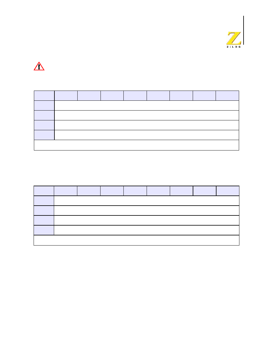
PS019915-1005
Watch-Dog
Timer
Z8 Encore!
�
64K Series
Product Specification
96
The 24-bit WDT Reload Value must not be set to a value less than
000004H
.
WDTU--WDT Reload Upper Byte
Most significant byte (MSB), Bits[23:16], of the 24-bit WDT reload value.
WDTH--WDT Reload High Byte
Middle byte, Bits[15:8], of the 24-bit WDT reload value.
Table 48. Watch-Dog Timer Reload Upper Byte Register (WDTU)
BITS
7
6
5
4
3
2
1
0
FIELD
WDTU
RESET
1
R/W
R/W*
ADDR
FF1H
R/W* - Read returns the current WDT count value. Write sets the desired Reload Value.
Table 49. Watch-Dog Timer Reload High Byte Register (WDTH)
BITS
7
6
5
4
3
2
1
0
FIELD
WDTH
RESET
1
R/W
R/W*
ADDR
FF2H
R/W* - Read returns the current WDT count value. Write sets the desired Reload Value.
Caution:
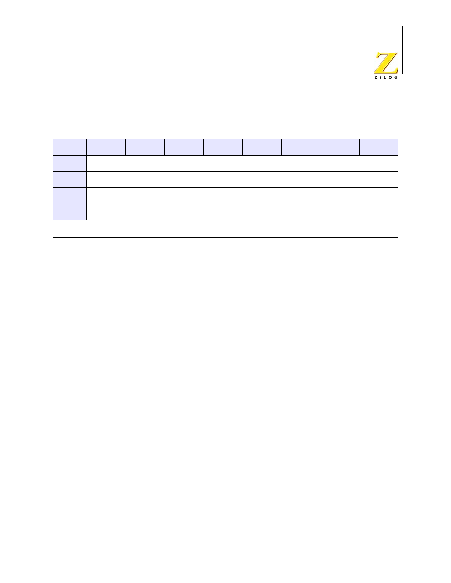
PS019915-1005
Watch-Dog
Timer
Z8 Encore!
�
64K Series
Product Specification
97
WDTL--WDT Reload Low
Least significant byte (LSB), Bits[7:0], of the 24-bit WDT reload value.
Table 50. Watch-Dog Timer Reload Low Byte Register (WDTL)
BITS
7
6
5
4
3
2
1
0
FIELD
WDTL
RESET
1
R/W
R/W*
ADDR
FF3H
R/W* - Read returns the current WDT count value. Write sets the desired Reload Value.

PS019915-1005
UART
Z8 Encore!
�
64K Series
Product Specification
98
UART
Overview
The Universal Asynchronous Receiver/Transmitter (UART) is a full-duplex communica-
tion channel capable of handling asynchronous data transfers. The UART uses a single
8-bit data mode with selectable parity. Features of the UART include:
�
8-bit asynchronous data transfer
�
Selectable even- and odd-parity generation and checking
�
Option of one or two Stop bits
�
Separate transmit and receive interrupts
�
Framing, parity, overrun and break detection
�
Separate transmit and receive enables
�
16-bit Baud Rate Generator (BRG)
�
Selectable Multiprocessor (9-bit) mode with three configurable interrupt schemes
�
Baud Rate Generator timer mode
�
Driver Enable output for external bus transceivers
Architecture
The UART consists of three primary functional blocks: transmitter, receiver, and baud rate
generator. The UART's transmitter and receiver function independently, but employ the
same baud rate and data format. Figure 13 illustrates the UART architecture.
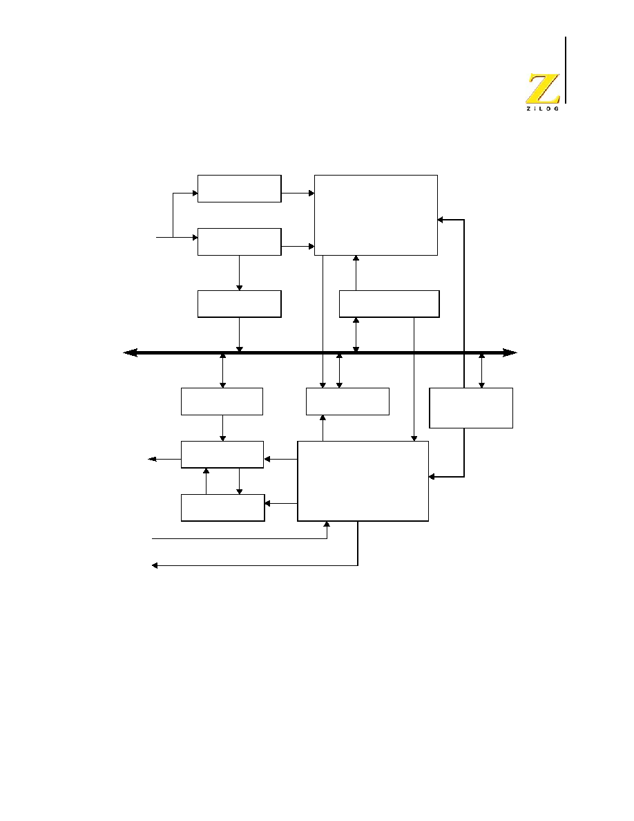
PS019915-1005
UART
Z8 Encore!
�
64K Series
Product Specification
99
Operation
Data Format
The UART always transmits and receives data in an 8-bit data format, least-significant bit
first. An even or odd parity bit can be optionally added to the data stream. Each character
begins with an active Low Start bit and ends with either 1 or 2 active High Stop bits.
Figures 14 and 15 illustrates the asynchronous data format employed by the UART with-
out parity and with parity, respectively.
Figure 13. UART Block Diagram
Receive Shifter
Receive Data
Transmit Data
Transmit Shift
TXD
RXD
System Bus
Parity Checker
Parity Generator
Receiver Control
Control Registers
Transmitter Control
CTS
Status Register
Register
Register
Register
Baud Rate
Generator
DE
with address compare
PS019915-1005
UART
Z8 Encore!
�
64K Series
Product Specification
100
Transmitting Data using the Polled Method
Follow these steps to transmit data using the polled method of operation:
1. Write to the UART Baud Rate High and Low Byte registers to set the desired baud
rate.
2. Enable the UART pin functions by configuring the associated GPIO Port pins for
alternate function operation.
3. If multiprocessor mode is desired, write to the UART Control 1 register to enable
Multiprocessor (9-bit) mode functions.
�
Set the MULTIPROCESSOR Mode Select (MPEN) to Enable
MULTIPROCESSOR mode.
4. Write to the UART Control 0 register to:
�
Set the transmit enable bit (TEN) to enable the UART for data transmission
�
If parity is desired and MULTIPROCESSOR mode is not enabled, set the parity
enable bit (PEN) and select either Even or Odd parity (PSEL).
Figure 14. UART Asynchronous Data Format without Parity
Figure 15. UART Asynchronous Data Format with Parity
Start
Bit0
Bit1
Bit2
Bit3
Bit4
Bit5
Bit6
Bit7
Data Field
lsb
msb
Idle State
of Line
Stop Bit(s)
1
2
1
0
Start
Bit0
Bit1
Bit2
Bit3
Bit4
Bit5
Bit6
Bit7
Parity
Data Field
lsb
msb
Idle State
of Line
Stop Bit(s)
1
2
1
0

PS019915-1005
UART
Z8 Encore!
�
64K Series
Product Specification
101
�
Set or clear the CTSE bit to enable or disable control from the remote receiver
using the CTS pin.
5. Check the TDRE bit in the UART Status 0 register to determine if the Transmit Data
register is empty (indicated by a 1). If empty, continue to Step 6. If the Transmit Data
register is full (indicated by a 0), continue to monitor the TDRE bit until the Transmit
Data register becomes available to receive new data.
6. Write the UART Control 1 register to select the outgoing address bit.
7. Set the MULTIPROCESSOR Bit Transmitter (MPBT) if sending an address byte, clear
it if sending a data byte.
8. Write the data byte to the UART Transmit Data register. The transmitter automatically
transfers the data to the Transmit Shift register and transmits the data.
9. If desired and MULTIPROCESSOR mode is enabled, make any changes to the
MULTIPROCESSOR Bit Transmitter (MPBT) value.
10. To transmit additional bytes, return to Step 5.
Transmitting Data using the Interrupt-Driven Method
The UART transmitter interrupt indicates the availability of the Transmit Data register to
accept new data for transmission. Follow these steps to configure the UART for interrupt-
driven data transmission:
1. Write to the UART Baud Rate High and Low Byte registers to set the desired baud
rate.
2. Enable the UART pin functions by configuring the associated GPIO Port pins for
alternate function operation.
3. Execute a DI instruction to disable interrupts.
4. Write to the Interrupt control registers to enable the UART Transmitter interrupt and
set the desired priority.
5. If MULTIPROCESSOR mode is desired, write to the UART Control 1 register to
enable MULTIPROCESSOR (9-bit) mode functions.
6. Set the MULTIPROCESSOR Mode Select (MPEN) to Enable MULTIPROCESSOR
mode
7. Write to the UART Control 0 register to:
�
Set the transmit enable bit (TEN) to enable the UART for data transmission
�
Enable parity, if desired and if multiprocessor mode is not enabled, and select
either even or odd parity
�
Set or clear the CTSE bit to enable or disable control from the remote receiver via
the CTS pin

PS019915-1005
UART
Z8 Encore!
�
64K Series
Product Specification
102
8. Execute an EI instruction to enable interrupts.
The UART is now configured for interrupt-driven data transmission. Because the UART
Transmit Data register is empty, an interrupt is generated immediately. When the UART
Transmit interrupt is detected, the associated interrupt service routine (ISR) performs the
following:
1. Write the UART Control 1 register to select the outgoing address bit:
�
Set the MULTIPROCESSOR Bit Transmitter (MPBT) if sending an address byte,
clear it if sending a data byte.
2. Write the data byte to the UART Transmit Data register. The transmitter automatically
transfers the data to the Transmit Shift register and transmits the data.
3. Clear the UART Transmit interrupt bit in the applicable Interrupt Request register.
4. Execute the IRET instruction to return from the interrupt-service routine and wait for
the Transmit Data register to again become empty.
Receiving Data using the Polled Method
Follow these steps to configure the UART for polled data reception:
1. Write to the UART Baud Rate High and Low Byte registers to set the desired baud
rate.
2. Enable the UART pin functions by configuring the associated GPIO Port pins for
alternate function operation.
3. Write to the UART Control 1 register to enable Multiprocessor mode functions, if
desired.
4. Write to the UART Control 0 register to:
�
Set the receive enable bit (REN) to enable the UART for data reception
�
Enable parity, if desired and if multiprocessor mode is not enabled, and select
either even or odd parity
5. Check the RDA bit in the UART Status 0 register to determine if the Receive Data
register contains a valid data byte (indicated by a 1). If RDA is set to 1 to indicate
available data, continue to Step 6. If the Receive Data register is empty (indicated by a
0), continue to monitor the RDA bit awaiting reception of the valid data.
6. Read data from the UART Receive Data register. If operating in Multiprocessor (9-bit)
mode, further actions may be required depending on the Multiprocessor Mode bits
MPMD[1:0].
7. Return to Step 5 to receive additional data.

PS019915-1005
UART
Z8 Encore!
�
64K Series
Product Specification
103
Receiving Data using the Interrupt-Driven Method
The UART Receiver interrupt indicates the availability of new data (as well as error con-
ditions). Follow these steps to configure the UART receiver for interrupt-driven operation:
1. Write to the UART Baud Rate High and Low Byte registers to set the desired baud
rate.
2. Enable the UART pin functions by configuring the associated GPIO Port pins for
alternate function operation.
3. Execute a
DI
instruction to disable interrupts.
4. Write to the Interrupt control registers to enable the UART Receiver interrupt and set
the desired priority.
5. Clear the UART Receiver interrupt in the applicable Interrupt Request register.
6. Write to the UART Control 1 Register to enable Multiprocessor (9-bit) mode
functions, if desired.
�
Set the MULTIPROCESSOR Mode Select (MPEN) to Enable Multiprocessor
mode
�
Set the MULTIPROCESSOR Mode Bits, MPMD[1:0], to select the desired
address matching scheme
�
Configure the UART to interrupt on received data and errors or errors only
(interrupt on errors only is unlikely to be useful for Z8 Encore! devices without a
DMA block)
7. Write the device address to the Address Compare Register (automatic multiprocessor
modes only).
8. Write to the UART Control 0 register to:
�
Set the receive enable bit (REN) to enable the UART for data reception
�
Enable parity, if desired and if multiprocessor mode is not enabled, and select
either even or odd parity
9. Execute an
EI
instruction to enable interrupts.
The UART is now configured for interrupt-driven data reception. When the UART
Receiver interrupt is detected, the associated interrupt service routine (ISR) performs the
following:
1. Check the UART Status 0 register to determine the source of the interrupt - error,
break, or received data.
2. If the interrupt was caused by data available, read the data from the UART Receive
Data register. If operating in MULTIPROCESSOR (9-bit) mode, further actions may
be required depending on the MULTIPROCESSOR Mode bits
MPMD[1:0]
.
3. Clear the UART Receiver interrupt in the applicable Interrupt Request register.

PS019915-1005
UART
Z8 Encore!
�
64K Series
Product Specification
104
4. Execute the IRET instruction to return from the interrupt-service routine and await
more data.
Clear To Send (CTS) Operation
The CTS pin, if enabled by the CTSE bit of the UART Control 0 register, performs flow
control on the outgoing transmit datastream. The Clear To Send (CTS) input pin is sam-
pled one system clock before beginning any new character transmission. To delay trans-
mission of the next data character, an external receiver must deassert CTS at least one
system clock cycle before a new data transmission begins. For multiple character trans-
missions, this would typically be done during Stop Bit transmission. If CTS deasserts in
the middle of a character transmission, the current character is sent completely.
MULTIPROCESSOR (9-bit) Mode
The UART has a MULTIPROCESSOR (9-bit) mode that uses an extra (9th) bit for selec-
tive communication when a number of processors share a common UART bus. In MULTI-
PROCESSOR mode (also referred to as 9-Bit mode), the multiprocessor bit (MP) is
transmitted immediately following the 8-bits of data and immediately preceding the Stop
bit(s) as illustrated in Figure 16. The character format is:
Figure 16. UART Asynchronous MULTIPROCESSOR Mode Data Format
In MULTIPROCESSOR (9-bit) mode, the Parity bit location (9th bit) becomes the MUL-
TIPROCESSOR control bit. The UART Control 1 and Status 1 registers provide MULTI-
PROCESSOR (9-bit) mode control and status information. If an automatic address
matching scheme is enabled, the UART Address Compare register holds the network
address of the device.
MULTIPROCESSOR (9-bit) Mode Receive Interrupts
When MULTIPROCESSOR mode is enabled, the UART only processes frames addressed
to it. The determination of whether a frame of data is addressed to the UART can be made
in hardware, software or some combination of the two, depending on the multiprocessor
configuration bits. In general, the address compare feature reduces the load on the CPU,
since it does not need to access the UART when it receives data directed to other devices
Start
Bit0
Bit1
Bit2
Bit3
Bit4
Bit5
Bit6
Bit7
MP
Data Field
lsb
msb
Idle State
of Line
Stop Bit(s)
1
2
1
0

PS019915-1005
UART
Z8 Encore!
�
64K Series
Product Specification
105
on the multi-node network. The following three MULTIPROCESSOR modes are avail-
able in hardware:
�
Interrupt on all address bytes
�
Interrupt on matched address bytes and correctly framed data bytes
�
Interrupt only on correctly framed data bytes
These modes are selected with MPMD[1:0] in the UART Control 1 Register. For all
MULTIPROCESSOR modes, bit MPEN of the UART Control 1 Register must be set to 1.
The first scheme is enabled by writing 01b to MPMD[1:0]. In this mode, all incoming
address bytes cause an interrupt, while data bytes never cause an interrupt. The interrupt
service routine must manually check the address byte that caused triggered the interrupt. If
it matches the UART address, the software clears MPMD[0]. At this point, each new
incoming byte interrupts the CPU. The software is then responsible for determining the
end of the frame. It checks for end-of-frame by reading the MPRX bit of the UART Status
1 Register for each incoming byte. If MPRX=1, a new frame has begun. If the address of
this new frame is different from the UART's address, then set MPMD[0] to 1 causing the
UART interrupts to go inactive until the next address byte. If the new frame's address
matches the UART's, the data in the new frame is processed as well.
The second scheme is enabled by setting MPMD[1:0] to 10b and writing the UART's
address into the UART Address Compare Register. This mode introduces more hardware
control, interrupting only on frames that match the UART's address. When an incoming
address byte does not match the UART's address, it is ignored. All successive data bytes in
this frame are also ignored. When a matching address byte occurs, an interrupt is issued
and further interrupts now occur on each succesive data byte. The first data byte in the
frame contains the NEWFRM=1 in the UART Status 1 Register. When the next address byte
occurs, the hardware compares it to the UART's address. If there is a match, the interrupts
continue sand the NEWFRM bit is set for the first byte of the new frame. If there is no
match, then the UART ignores all incoming bytes until the next address match.
The third scheme is enabled by setting MPMD[1:0] to 11b and by writing the UART's
address into the UART Address Compare Register. This mode is identical to the second
scheme, except that there are no interrupts on address bytes. The first data byte of each
frame is still accompanied by a NEWFRM assertion.
External Driver Enable
The UART provides a Driver Enable (
DE
) signal for off-chip bus transceivers. This feature
reduces the software overhead associated with using a GPIO pin to control the transceiver
when communicating on a multi-transceiver bus, such as RS-485.
Driver Enable is an active High signal that envelopes the entire transmitted data frame
including parity and Stop bits as illustrated in Figure 17. The Driver Enable signal asserts
when a byte is written to the UART Transmit Data register. The Driver Enable signal
asserts at least one UART bit period and no greater than two UART bit periods before the
PS019915-1005
UART
Z8 Encore!
�
64K Series
Product Specification
106
Start bit is transmitted. This timing allows a setup time to enable the transceiver. The
Driver Enable signal deasserts one system clock period after the last Stop bit is transmit-
ted. This one system clock delay allows both time for data to clear the transceiver before
disabling it, as well as the ability to determine if another character follows the current
character. In the event of back to back characters (new data must be written to the Trans-
mit Data Register before the previous character is completely transmitted) the
DE
signal is
not deasserted between characters. The
DEPOL
bit in the UART Control Register 1 sets the
polarity of the Driver Enable signal.
Figure 17. UART Driver Enable Signal Timing (shown with 1 Stop Bit and Parity)
The
Driver Enable to Start
bit setup time is calculated as follows:
UART Interrupts
The UART features separate interrupts for the transmitter and the receiver. In addition,
when the UART primary functionality is disabled, the Baud Rate Generator can also func-
tion as a basic timer with interrupt capability.
Transmitter Interrupts
The transmitter generates a single interrupt when the Transmit Data Register Empty bit
(
TDRE
) is set to 1. This indicates that the transmitter is ready to accept new data for trans-
mission. The
TDRE
interrupt occurs after the Transmit shift register has shifted the first bit
of data out. At this point, the Transmit Data register may be written with the next character
to send. This provides 7 bit periods of latency to load the Transmit Data register before the
Transmit shift register completes shifting the current character. Writing to the UART
Transmit Data register clears the
TDRE
bit to 0.
Start
Bit0
Bit1
Bit2
Bit3
Bit4
Bit5
Bit6
Bit7
Parity
Data Field
lsb
msb
Idle State
of Line
Stop Bit
1
1
0
0
1
DE
1
Baud Rate (Hz)
-------------------------------------
DE to Start Bit Setup Time (s)
2
Baud Rate (Hz)
-------------------------------------

PS019915-1005
UART
Z8 Encore!
�
64K Series
Product Specification
107
Receiver Interrupts
The receiver generates an interrupt when any of the following occurs:
�
A data byte has been received and is available in the UART Receive Data register.
This interrupt can be disabled independent of the other receiver interrupt sources. The
received data interrupt occurs once the receive character has been received and placed
in the Receive Data register. Software must respond to this received data available
condition before the next character is completely received to avoid an overrun error.
Note that in multiprocessor mode (MPEN = 1), the receive data interrupts are
dependent on the multiprocessor configuration and the most recent address byte.
�
A break is received
�
An overrun is detected
�
A data framing error is detected
UART Overrun Errors
When an overrun error condition occurs the UART prevents overwriting of the valid data
currently in the Receive Data register. The Break Detect and Overrun status bits are not
displayed until after the valid data has been read.
After the valid data has been read, the UART Status 0 register is updated to indicate the
overrun condition (and Break Detect, if applicable). The
RDA
bit is set to 1 to indicate that
the Receive Data register contains a data byte. However, because the overrun error
occurred, this byte may not contain valid data and should be ignored. The
BRKD
bit indi-
cates if the overrun was caused by a break condition on the line. After reading the status
byte indicating an overrun error, the Receive Data register must be read again to clear the
error bits is the UART Status 0 register. Updates to the Receive Data register occur only
when the next data word is received.
UART Data and Error Handling Procedure
Figure 18 illustrates the recommended procedure for use in UART receiver interrupt ser-
vice routines.
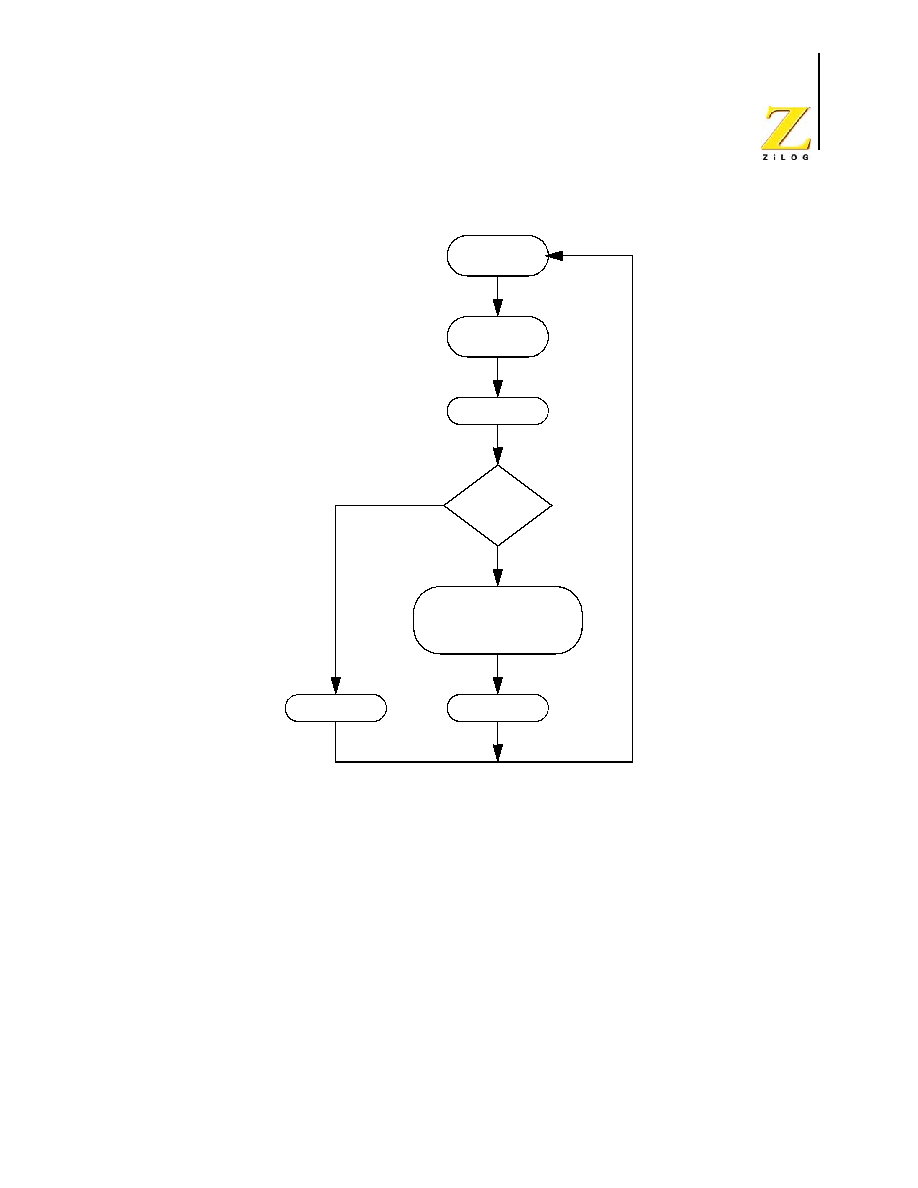
PS019915-1005
UART
Z8 Encore!
�
64K Series
Product Specification
108
Figure 18. UART Receiver Interrupt Service Routine Flow
Baud Rate Generator Interrupts
If the Baud Rate Generator (BRG) interrupt enable is set, the UART Receiver interrupt
asserts when the UART Baud Rate Generator reloads. This action allows the Baud Rate
Generator to function as an additional counter if the UART functionality is not employed.
UART Baud Rate Generator
The UART Baud Rate Generator creates a lower frequency baud rate clock for data trans-
mission. The input to the Baud Rate Generator is the system clock. The UART Baud Rate
High and Low Byte registers combine to create a 16-bit baud rate divisor value
Receiver
Errors?
No
Yes
Read Status
Discard Data
Read Data which
Interrupt
Receiver
Ready
clears RDA bit and
resets error bits
Read Data
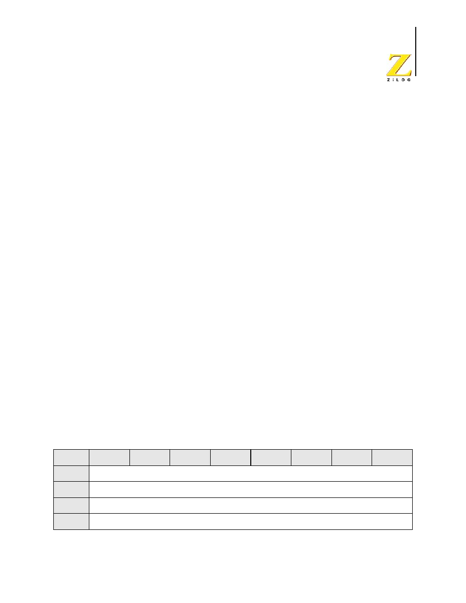
PS019915-1005
UART
Z8 Encore!
�
64K Series
Product Specification
109
(BRG[15:0]) that sets the data transmission rate (baud rate) of the UART. The UART data
rate is calculated using the following equation:
When the UART is disabled, the Baud Rate Generator can function as a basic 16-bit timer
with interrupt on time-out. To configure the Baud Rate Generator as a timer with interrupt
on time-out, complete the following procedure:
1. Disable the UART by clearing the REN and TEN bits in the UART Control 0 register
to 0.
2. Load the desired 16-bit count value into the UART Baud Rate High and Low Byte
registers.
3. Enable the Baud Rate Generator timer function and associated interrupt by setting the
BRGCTL
bit in the UART Control 1 register to 1.
When configured as a general purpose timer, the interrupt interval is calculated using the
following equation:
Interrupt Interval (s) = System Clock Period (s) �BRG[15:0]
]
UART Control Register Definitions
The UART control registers support the UART and the associated Infrared Encoder/
Decoders. For more information on the infrared operation, refer to the Infrared Encoder/
Decoder chapter on page 120.
UART Transmit Data Register
Data bytes written to the UART Transmit Data register (Table 51) are shifted out on the
TXDx pin. The Write-only UART Transmit Data register shares a Register File address
with the Read-only UART Receive Data register.
Table 51. UART Transmit Data Register (UxTXD)
BITS
7
6
5
4
3
2
1
0
FIELD
TXD
RESET
X
R/W
W
ADDR
F40H and F48H
UART Data Rate (bits/s)
System Clock Frequency (Hz)
16 UART Baud Rate Divisor Value
�
----------------------------------------------------------------------------------------------
=
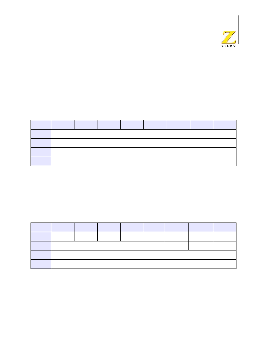
PS019915-1005
UART
Z8 Encore!
�
64K Series
Product Specification
110
TXD--Transmit Data
UART transmitter data byte to be shifted out through the TXDx pin.
UART Receive Data Register
Data bytes received through the RXDx pin are stored in the UART Receive Data register
(Table 52). The Read-only UART Receive Data register shares a Register File address
with the Write-only UART Transmit Data register.
RXD--Receive Data
UART receiver data byte from the RXDx pin
UART Status 0 Register
The UART Status 0 and Status 1 registers (Table 53 and 54) identify the current UART
operating configuration and status.
RDA--Receive Data Available
This bit indicates that the UART Receive Data register has received data. Reading the
UART Receive Data register clears this bit.
0 = The UART Receive Data register is empty.
1 = There is a byte in the UART Receive Data register.
Table 52. UART Receive Data Register (UxRXD)
BITS
7
6
5
4
3
2
1
0
FIELD
RXD
RESET
X
R/W
R
ADDR
F40H and F48H
Table 53. UART Status 0 Register (UxSTAT0)
BITS
7
6
5
4
3
2
1
0
FIELD
RDA
PE
OE
FE
BRKD
TDRE
TXE
CTS
RESET
0
1
X
R/W
R
ADDR
F41H and F49H

PS019915-1005
UART
Z8 Encore!
�
64K Series
Product Specification
111
PE--Parity Error
This bit indicates that a parity error has occurred. Reading the UART Receive Data regis-
ter clears this bit.
0 = No parity error occurred.
1 = A parity error occurred.
OE--Overrun Error
This bit indicates that an overrun error has occurred. An overrun occurs when new data is
received and the UART Receive Data register has not been read. If the RDA bit is reset to
0, then reading the UART Receive Data register clears this bit.
0 = No overrun error occurred.
1 = An overrun error occurred.
FE--Framing Error
This bit indicates that a framing error (no Stop bit following data reception) was detected.
Reading the UART Receive Data register clears this bit.
0 = No framing error occurred.
1 = A framing error occurred.
BRKD--Break Detect
This bit indicates that a break occurred. If the data bits, parity/multiprocessor bit, and Stop
bit(s) are all zeros then this bit is set to 1. Reading the UART Receive Data register clears
this bit.
0 = No break occurred.
1 = A break occurred.
TDRE--Transmitter Data Register Empty
This bit indicates that the UART Transmit Data register is empty and ready for additional
data. Writing to the UART Transmit Data register resets this bit.
0 = Do not write to the UART Transmit Data register.
1 = The UART Transmit Data register is ready to receive an additional byte to be transmit-
ted.
TXE--Transmitter Empty
This bit indicates that the transmit shift register is empty and character transmission is fin-
ished.
0 = Data is currently transmitting.
1 = Transmission is complete.
CTS--CTS signal
When this bit is read it returns the level of the CTS signal.
PS019915-1005
UART
Z8 Encore!
�
64K Series
Product Specification
112
Reserved--Must be 0.
NEWFRM--Status bit denoting the start of a new frame. Reading the UART Receive
Data register resets this bit to 0.
0 = The current byte is not the first data byte of a new frame.
1 = The current byte is the first data byte of a new frame.
MPRX--Multiprocessor Receive
Returns the value of the last multiprocessor bit received. Reading from the UART Receive
Data register resets this bit to 0.
UART Control 0 and Control 1 Registers
The UART Control 0 and Control 1 registers (Tables 55 and 56) configure the properties
of the UART's transmit and receive operations. The UART Control registers must not
been written while the UART is enabled.
TEN--Transmit Enable
This bit enables or disables the transmitter. The enable is also controlled by the CTS signal
and the CTSE bit. If the CTS signal is low and the CTSE bit is 1, the transmitter is
UART Status 1 Register
This register contains multiprocessor control and status bits.
Table 54. UART Status 1 Register (UxSTAT1)
BITS
7
6
5
4
3
2
1
0
FIELD
Reserved
NEWFRM
MPRX
RESET
0
R/W
R
R/W
R
ADDR
F44H and F4CH
Table 55. UART Control 0 Register (UxCTL0)
BITS
7
6
5
4
3
2
1
0
FIELD
TEN
REN
CTSE
PEN
PSEL
SBRK
STOP
LBEN
RESET
0
R/W
R/W
ADDR
F42H and F4AH

PS019915-1005
UART
Z8 Encore!
�
64K Series
Product Specification
113
enabled.
0 = Transmitter disabled.
1 = Transmitter enabled.
REN--Receive Enable
This bit enables or disables the receiver.
0 = Receiver disabled.
1 = Receiver enabled.
CTSE--CTS Enable
0 = The CTS signal has no effect on the transmitter.
1 = The UART recognizes the CTS signal as an enable control from the transmitter.
PEN--Parity Enable
This bit enables or disables parity. Even or odd is determined by the PSEL bit. It is over-
ridden by the
MPEN
bit.
0 = Parity is disabled.
1 = The transmitter sends data with an additional parity bit and the receiver receives an
additional parity bit.
PSEL--Parity Select
0 = Even parity is transmitted and expected on all received data.
1 = Odd parity is transmitted and expected on all received data.
SBRK--Send Break
This bit pauses or breaks data transmission. Sending a break interrupts any transmission in
progress, so ensure that the transmitter has finished sending data before setting this bit.
0 = No break is sent.
1 = The output of the transmitter is zero.
STOP--Stop Bit Select
0 = The transmitter sends one stop bit.
1 = The transmitter sends two stop bits.
LBEN--Loop Back Enable
0 = Normal operation.
1 = All transmitted data is looped back to the receiver.
Table 56. UART Control 1 Register (UxCTL1)
BITS
7
6
5
4
3
2
1
0
FIELD
MPMD[1]
MPEN
MPMD[0]
MPBT
DEPOL
BRGCTL
RDAIRQ
IREN
RESET
0
R/W
R/W
ADDR
F43H and F4BH

PS019915-1005
UART
Z8 Encore!
�
64K Series
Product Specification
114
MPMD[1:0]--MULTIPROCESSOR Mode
If MULTIPROCESSOR (9-bit) mode is enabled,
00 = The UART generates an interrupt request on all received bytes (data and address).
01 = The UART generates an interrupt request only on received address bytes.
10 = The UART generates an interrupt request when a received address byte matches the
value stored in the Address Compare Register and on all successive data bytes until an
address mismatch occurs.
11 = The UART generates an interrupt request on all received data bytes for which the
most recent address byte matched the value in the Address Compare Register.
MPEN--MULTIPROCESSOR (9-bit) Enable
This bit is used to enable MULTIPROCESSOR (9-bit) mode.
0 = Disable MULTIPROCESSOR (9-bit) mode.
1 = Enable MULTIPROCESSOR (9-bit) mode.
MPBT--MULTIPROCESSOR Bit Transmit
This bit is applicable only when MULTIPROCESSOR (9-bit) mode is enabled.
0 = Send a 0 in the multiprocessor bit location of the data stream (9th bit).
1 = Send a 1 in the multiprocessor bit location of the data stream (9th bit).
DEPOL--Driver Enable Polarity
0 =
DE
signal is Active High.
1 =
DE
signal is Active Low.
BRGCTL--Baud Rate Control
This bit causes different UART behavior depending on whether the UART receiver is
enabled (
REN
= 1 in the UART Control 0 Register).
When the UART receiver is not enabled, this bit determines whether the Baud Rate Gener-
ator issues interrupts.
0 = Reads from the Baud Rate High and Low Byte registers return the BRG Reload Value
1 = The Baud Rate Generator generates a receive interrupt when it counts down to 0.
Reads from the Baud Rate High and Low Byte registers return the current BRG count
value.
When the UART receiver is enabled, this bit allows reads from the Baud Rate Registers to
return the BRG count value instead of the Reload Value.
0 = Reads from the Baud Rate High and Low Byte registers return the BRG Reload Value.
1 = Reads from the Baud Rate High and Low Byte registers return the current BRG count
value. Unlike the Timers, there is no mechanism to latch the High Byte when the Low
Byte is read.
RDAIRQ--Receive Data Interrupt Enable
0 = Received data and receiver errors generates an interrupt request to the Interrupt Con-
troller.
1 = Received data does not generate an interrupt request to the Interrupt Controller. Only
receiver errors generate an interrupt request.
PS019915-1005
UART
Z8 Encore!
�
64K Series
Product Specification
115
IREN--Infrared Encoder/Decoder Enable
0 = Infrared Encoder/Decoder is disabled. UART operates normally operation.
1 = Infrared Encoder/Decoder is enabled. The UART transmits and receives data through
the Infrared Encoder/Decoder.
UART Address Compare Register
The UART Address Compare register (Table 57) stores the multi-node network address of
the UART. When the MPMD[1] bit of UART Control Register 0 is set, all incoming
address bytes are compared to the value stored in the Address Compare register. Receive
interrupts and RDA assertions only occur in the event of a match.
COMP_ADDR--Compare Address
This 8-bit value is compared to the incoming address bytes.
UART Baud Rate High and Low Byte Registers
The UART Baud Rate High and Low Byte registers (Tables 58 and 59) combine to create
a 16-bit baud rate divisor value (BRG[15:0]) that sets the data transmission rate (baud
rate) of the UART. To configure the Baud Rate Generator as a timer with interrupt on
time-out, complete the following procedure:
1. Disable the UART by clearing the REN and TEN bits in the UART Control 0 register
to 0.
2. Load the desired 16-bit count value into the UART Baud Rate High and Low Byte
registers.
3. Enable the Baud Rate Generator timer function and associated interrupt by setting the
BRGCTL
bit in the UART Control 1 register to 1.
When congured as a general purpose timer, the UART BRG interrupt interval is calculated
using the following equation:
UART BRG Interrupt Interval (s) = System Clock Period (s) �BRG[15:0]
]
Table 57. UART Address Compare Register (UxADDR)
BITS
7
6
5
4
3
2
1
0
FIELD
COMP_ADDR
RESET
0
R/W
R/W
ADDR
F45H and F4DH
PS019915-1005
UART
Z8 Encore!
�
64K Series
Product Specification
116
For a given UART data rate, the integer baud rate divisor value is calculated using the fol-
lowing equation:
The baud rate error relative to the desired baud rate is calculated using the following equa-
tion:
For reliable communication, the UART baud rate error must never exceed 5 percent.
Table 60 provides information on data rate errors for popular baud rates and commonly
used crystal oscillator frequencies.
Table 58. UART Baud Rate High Byte Register (UxBRH)
BITS
7
6
5
4
3
2
1
0
FIELD
BRH
RESET
1
R/W
R/W
ADDR
F46H and F4EH
Table 59. UART Baud Rate Low Byte Register (UxBRL)
BITS
7
6
5
4
3
2
1
0
FIELD
BRL
RESET
1
R/W
R/W
ADDR
F47H and F4FH
UART Baud Rate Divisor Value (BRG)
Round
System Clock Frequency (Hz)
16 UART Data Rate (bits/s)
�
----------------------------------------------------------------------------
=
UART Baud Rate Error (%)
100
Actual Data Rate
Desired Data Rate
Desired Data Rate
---------------------------------------------------------------------------------------------------
�
=

PS019915-1005
UART
Z8 Encore!
�
64K Series
Product Specification
117
Table 60. UART Baud Rates
20.0 MHz System Clock
18.432 MHz System Clock
Desired Rate
BRG Divisor
Actual Rate
Error
Desired Rate
BRG Divisor
Actual Rate
Error
(kHz)
(Decimal)
(kHz)
(%)
(kHz)
(Decimal)
(kHz)
(%)
1250.0
1
1250.0
0.00
1250.0
1
1152.0
-7.84%
625.0
2
625.0
0.00
625.0
2
576.0
-7.84%
250.0
5
250.0
0.00
250.0
5
230.4
-7.84%
115.2
11
113.6
-1.36
115.2
10
115.2
0.00
57.6
22
56.8
-1.36
57.6
20
57.6
0.00
38.4
33
37.9
-1.36
38.4
30
38.4
0.00
19.2
65
19.2
0.16
19.2
60
19.2
0.00
9.60
130
9.62
0.16
9.60
120
9.60
0.00
4.80
260
4.81
0.16
4.80
240
4.80
0.00
2.40
521
2.40
-0.03
2.40
480
2.40
0.00
1.20
1042
1.20
-0.03
1.20
960
1.20
0.00
0.60
2083
0.60
0.02
0.60
1920
0.60
0.00
0.30
4167
0.30
-0.01
0.30
3840
0.30
0.00
16.667 MHz System Clock
11.0592 MHz System Clock
Desired Rate
BRG Divisor
Actual Rate
Error
Desired Rate
BRG Divisor
Actual Rate
Error
(kHz)
(Decimal)
(kHz)
(%)
(kHz)
(Decimal)
(kHz)
(%)
1250.0
1
1041.69
-16.67
1250.0
N/A
N/A
N/A
625.0
2
520.8
-16.67
625.0
1
691.2
10.59
250.0
4
260.4
4.17
250.0
3
230.4
-7.84
115.2
9
115.7
0.47
115.2
6
115.2
0.00
57.6
18
57.87
0.47
57.6
12
57.6
0.00
38.4
27
38.6
0.47
38.4
18
38.4
0.00
19.2
54
19.3
0.47
19.2
36
19.2
0.00
9.60
109
9.56
-0.45
9.60
72
9.60
0.00
4.80
217
4.80
-0.83
4.80
144
4.80
0.00
2.40
434
2.40
0.01
2.40
288
2.40
0.00
1.20
868
1.20
0.01
1.20
576
1.20
0.00
0.60
1736
0.60
0.01
0.60
1152
0.60
0.00

PS019915-1005
UART
Z8 Encore!
�
64K Series
Product Specification
118
0.30
3472
0.30
0.01
0.30
2304
0.30
0.00
10.0 MHz System Clock
5.5296 MHz System Clock
Desired Rate
BRG Divisor
Actual Rate
Error
Desired Rate
BRG Divisor
Actual Rate
Error
(kHz)
(Decimal)
(kHz)
(%)
(kHz)
(Decimal)
(kHz)
(%)
1250.0
N/A
N/A
N/A
1250.0
N/A
N/A
N/A
625.0
1
625.0
0.00
625.0
N/A
N/A
N/A
250.0
3
208.33
-16.67
250.0
1
345.6
38.24
115.2
5
125.0
8.51
115.2
3
115.2
0.00
57.6
11
56.8
-1.36
57.6
6
57.6
0.00
38.4
16
39.1
1.73
38.4
9
38.4
0.00
19.2
33
18.9
0.16
19.2
18
19.2
0.00
9.60
65
9.62
0.16
9.60
36
9.60
0.00
4.80
130
4.81
0.16
4.80
72
4.80
0.00
2.40
260
2.40
-0.03
2.40
144
2.40
0.00
1.20
521
1.20
-0.03
1.20
288
1.20
0.00
0.60
1042
0.60
-0.03
0.60
576
0.60
0.00
0.30
2083
0.30
0.2
0.30
1152
0.30
0.00
3.579545 MHz System Clock
1.8432 MHz System Clock
Desired Rate
BRG Divisor
Actual Rate
Error
Desired Rate
BRG Divisor
Actual Rate
Error
(kHz)
(Decimal)
(kHz)
(%)
(kHz)
(Decimal)
(kHz)
(%)
1250.0
N/A
N/A
N/A
1250.0
N/A
N/A
N/A
625.0
N/A
N/A
N/A
625.0
N/A
N/A
N/A
250.0
1
223.72
-10.51
250.0
N/A
N/A
N/A
115.2
2
111.9
-2.90
115.2
1
115.2
0.00
57.6
4
55.9
-2.90
57.6
2
57.6
0.00
38.4
6
37.3
-2.90
38.4
3
38.4
0.00
19.2
12
18.6
-2.90
19.2
6
19.2
0.00
9.60
23
9.73
1.32
9.60
12
9.60
0.00
4.80
47
4.76
-0.83
4.80
24
4.80
0.00
2.40
93
2.41
0.23
2.40
48
2.40
0.00
1.20
186
1.20
0.23
1.20
96
1.20
0.00
Table 60. UART Baud Rates (Continued)

PS019915-1005
UART
Z8 Encore!
�
64K Series
Product Specification
119
0.60
373
0.60
-0.04
0.60
192
0.60
0.00
0.30
746
0.30
-0.04
0.30
384
0.30
0.00
Table 60. UART Baud Rates (Continued)
Z8 Encore!
�
64K Series
Product Specification
PS019915-1005
Infrared
Encoder/Decoder
120
Infrared Encoder/Decoder
Overview
The 64K Series products contain two fully-functional, high-performance UART to Infra-
red Encoder/Decoders (Endecs). Each Infrared Endec is integrated with an on-chip UART
to allow easy communication between the 64K Series and IrDA Physical Layer Specifica-
tion, Version 1.3-compliant infrared transceivers. Infrared communication provides
secure, reliable, low-cost, point-to-point communication between PCs, PDAs, cell phones,
printers and other infrared enabled devices.
Architecture
Figure 19 illustrates the architecture of the Infrared Endec.
Figure 19. Infrared Data Communication System Block Diagram
Interrupt
Signal
RXD
TXD
Infrared
Encoder/Decoder
UART
RxD
TxD
System
Clock
I/O
Address
Data
Infrared
Transceiver
RXD
TXD
Baud Rate
Clock
(Endec)
ZiLOG
ZHX1810

PS019915-1005
Infrared
Encoder/Decoder
Z8 Encore!
�
64K Series
Product Specification
121
Operation
When the Infrared Endec is enabled, the transmit data from the associated on-chip UART
is encoded as digital signals in accordance with the IrDA standard and output to the infra-
red transceiver via the TXD pin. Likewise, data received from the infrared transceiver is
passed to the Infrared Endec via the RXD pin, decoded by the Infrared Endec, and then
passed to the UART. Communication is half-duplex, which means simultaneous data
transmission and reception is not allowed.
The baud rate is set by the UART's Baud Rate Generator and supports IrDA standard baud
rates from 9600 baud to 115.2 Kbaud. Higher baud rates are possible, but do not meet
IrDA specifications. The UART must be enabled to use the Infrared Endec. The Infrared
Endec data rate is calculated using the following equation:
Transmitting IrDA Data
The data to be transmitted using the infrared transceiver is first sent to the UART. The
UART's transmit signal (TXD) and baud rate clock are used by the IrDA to generate the
modulation signal (IR_TXD) that drives the infrared transceiver. Each UART/Infrared
data bit is 16-clocks wide. If the data to be transmitted is 1, the IR_TXD signal remains
low for the full 16-clock period. If the data to be transmitted is 0, a 3-clock high pulse is
output following a 7-clock low period. After the 3-clock high pulse, a 6-clock low pulse is
output to complete the full 16-clock data period. Figure 20 illustrates IrDA data transmis-
sion. When the Infrared Endec is enabled, the UART's TXD signal is internal to the 64K
Series products while the IR_TXD signal is output through the TXD pin.
Infrared Data Rate (bits/s)
System Clock Frequency (Hz)
16 UART Baud Rate Divisor Value
�
----------------------------------------------------------------------------------------------
=
PS019915-1005
Infrared
Encoder/Decoder
Z8 Encore!
�
64K Series
Product Specification
122
Figure 20. Infrared Data Transmission
Receiving IrDA Data
Data received from the infrared transceiver via the IR_RXD signal through the
RXD
pin is
decoded by the Infrared Endec and passed to the UART. The UART's baud rate clock is
used by the Infrared Endec to generate the demodulated signal (RXD) that drives the
UART. Each UART/Infrared data bit is 16-clocks wide. Figure 21 illustrates data recep-
tion. When the Infrared Endec is enabled, the UART's RXD signal is internal to the 64K
Series products while the IR_RXD signal is received through the
RXD
pin.
Baud Rate
IR_TXD
UART's
16-clock
period
Start Bit = 0
Data Bit 0 = 1
Data Bit 1 = 0
Data Bit 2 = 1
Data Bit 3 = 1
7-clock
delay
3-clock
pulse
TXD
Clock
PS019915-1005
Infrared
Encoder/Decoder
Z8 Encore!
�
64K Series
Product Specification
123
Figure 21. Infrared Data Reception
The system clock frequency must be at least 1.0MHz to ensure proper re-
ception of the 1.6
s minimum width pulses allowed by the IrDA standard.
Endec Receiver Synchronization
The IrDA receiver uses a local baud rate clock counter (0 to 15 clock periods) to generate
an input stream for the UART and to create a sampling window for detection of incoming
pulses. The generated UART input (UART RXD) is delayed by 8 baud rate clock periods
with respect to the incoming IrDA data stream. When a falling edge in the input data
stream is detected, the Endec counter is reset. When the count reaches a value of 8, the
UART RXD value is updated to reflect the value of the decoded data. When the count
reaches 12 baud clock periods, the sampling window for the next incoming pulse opens.
The window remains open until the count again reaches 8 (or in other words 24 baud clock
periods since the previous pulse was detected). This gives the Endec a sampling window
of minus four baudrate clocks to plus eight baudrate clocks around the expected time of an
incoming pulse. If an incoming pulse is detected inside this window this process is
repeated. If the incoming data is a logical 1 (no pulse), the Endec returns to the initial state
and waits for the next falling edge. As each falling edge is detected, the Endec clock
counter is reset, resynchronizing the Endec to the incoming signal. This action allows the
Endec to tolerate jitter and baud rate errors in the incoming data stream. Resynchronizing
the Endec does not alter the operation of the UART, which ultimately receives the data.
The UART is only synchronized to the incoming data stream when a Start bit is received.
Baud Rate
UART's
IR_RXD
16-clock
period
Start Bit = 0
Data Bit 0 = 1
Data Bit 1 = 0
Data Bit 2 = 1
Data Bit 3 = 1
8-clock
delay
Clock
RXD
16-clock
period
16-clock
period
16-clock
period
16-clock
period
Start Bit = 0
Data Bit 0 = 1
Data Bit 1 = 0
Data Bit 2 = 1
Data Bit 3 = 1
min. 1.6
s
pulse
Caution:

PS019915-1005
Infrared
Encoder/Decoder
Z8 Encore!
�
64K Series
Product Specification
124
Infrared Encoder/Decoder Control Register Definitions
All Infrared Endec configuration and status information is set by the UART control regis-
ters as defined beginning on
page 109
.
To prevent spurious signals during IrDA data transmission, set the IREN
bit in the UARTx Control 1 register to 1 to enable the Infrared Encoder/
Decoder before enabling the GPIO Port alternate function for the corre-
sponding pin.
Caution:
Z8 Encore!
�
64K Series
Product Specification
PS019915-1005
Serial
Peripheral
Interface
125
Serial Peripheral Interface
Overview
The Serial Peripheral Interface
TM
(SPI) is a synchronous interface allowing several SPI-
type devices to be interconnected. SPI-compatible devices include EEPROMs, Analog-to-
Digital Converters, and ISDN devices. Features of the SPI include:
�
Full-duplex, synchronous, character-oriented communication
�
Four-wire interface
�
Data transfers rates up to a maximum of one-half the system clock frequency
�
Error detection
�
Dedicated Baud Rate Generator
Architecture
The SPI may be configured as either a Master (in single or multi-master systems) or a
Slave as illustrated in Figures 22 through 24.
Figure 22. SPI Configured as a Master in a Single Master, Single Slave System
SPI Master
8-bit Shift Register
Bit 0
Bit 7
MISO
MOSI
SCK
SS
To Slave's SS Pin
From Slave
To Slave
To Slave
Baud Rate
Generator
PS019915-1005
Serial
Peripheral
Interface
Z8 Encore!
�
64K Series
Product Specification
126
Figure 23. SPI Configured as a Master in a Single Master, Multiple Slave System
Figure 24. SPI Configured as a Slave
Operation
The SPI is a full-duplex, synchronous, character-oriented channel that supports a four-wire
interface (serial clock, transmit, receive and Slave select). The SPI block consists of a
transmit/receive shift register, a Baud Rate (clock) Generator and a control unit.
SPI Master
8-bit Shift Register
Bit 0
Bit 7
MISO
MOSI
SCK
GPIO
To Slave #2's SS Pin
From Slave
To Slave
To Slave
SS
Baud Rate
Generator
VCC
GPIO
To Slave #1's SS Pin
SPI Slave
8-bit Shift Register
Bit 7
Bit 0
MISO
MOSI
SCK
SS
From Master
To Master
From Master
From Master

PS019915-1005
Serial
Peripheral
Interface
Z8 Encore!
�
64K Series
Product Specification
127
During an SPI transfer, data is sent and received simultaneously by both the Master and
the Slave SPI devices. Separate signals are required for data and the serial clock. When an
SPI transfer occurs, a multi-bit (typically 8-bit) character is shifted out one data pin and an
multi-bit character is simultaneously shifted in on a second data pin. An 8-bit shift register
in the Master and another 8-bit shift register in the Slave are connected as a circular buffer.
The SPI shift register is single-buffered in the transmit and receive directions. New data to
be transmitted cannot be written into the shift register until the previous transmission is
complete and receive data (if valid) has been read.
SPI Signals
The four basic SPI signals are:
�
MISO (Master-In, Slave-Out)
�
MOSI (Master-Out, Slave-In)
�
SCK (SPI Serial Clock)
�
SS (Slave Select)
The following paragraphs discuss these SPI signals. Each signal is described in both Mas-
ter and Slave modes.
Master-In, Slave-Out
The Master-In, Slave-Out (MISO) pin is configured as an input in a Master device and as
an output in a Slave device. It is one of the two lines that transfer serial data, with the most
significant bit sent first. The MISO pin of a Slave device is placed in a high-impedance
state if the Slave is not selected. When the SPI is not enabled, this signal is in a high-
impedance state.
Master-Out, Slave-In
The Master-Out, Slave-In (MOSI) pin is configured as an output in a Master device and as
an input in a Slave device. It is one of the two lines that transfer serial data, with the most
significant bit sent first. When the SPI is not enabled, this signal is in a high-impedance
state.
Serial Clock
The Serial Clock (SCK) synchronizes data movement both in and out of the device
through its MOSI and MISO pins. In MASTER mode, the SPI's Baud Rate Generator cre-
ates the serial clock. The Master drives the serial clock out its own SCK pin to the Slave's
SCK pin. When the SPI is configured as a Slave, the SCK pin is an input and the clock sig-
nal from the Master synchronizes the data transfer between the Master and Slave devices.
Slave devices ignore the SCK signal, unless the SS pin is asserted. When configured as a
slave, the SPI block requires a minimum SCK period of greater than or equal to 8 times
the system (XIN) clock period.

PS019915-1005
Serial
Peripheral
Interface
Z8 Encore!
�
64K Series
Product Specification
128
The Master and Slave are each capable of exchanging a character of data during a
sequence of NUMBITS clock cycles (refer to NUMBITS field in the SPIMODE register).
In both Master and Slave SPI devices, data is shifted on one edge of the SCK and is sam-
pled on the opposite edge where data is stable. Edge polarity is determined by the SPI
phase and polarity control.
Slave Select
The active Low Slave Select (SS) input signal selects a Slave SPI device. SS must be Low
prior to all data communication to and from the Slave device. SS must stay Low for the
full duration of each character transferred. The SS signal may stay Low during the transfer
of multiple characters or may deassert between each character.
When the SPI is configured as the only Master in an SPI system, the SS pin can be set as
either an input or an output. For communication between the Z8F642x familyZ8R642x
family device's SPI Master and external Slave devices, the SS signal, as an output, can
assert the SS input pin on one of the Slave devices. Other GPIO output pins can also be
employed to select external SPI Slave devices.
When the SPI is configured as one Master in a multi-master SPI system, the SS pin must
be set as an input. The SS input signal on the Master must be High. If the SS signal goes
Low (indicating another Master is driving the SPI bus), a Collision error flag is set in the
SPI Status register.
SPI Clock Phase and Polarity Control
The SPI supports four combinations of serial clock phase and polarity using two bits in the
SPI Control register. The clock polarity bit, CLKPOL, selects an active high or active low
clock and has no effect on the transfer format. Table 61 lists the SPI Clock Phase and
Polarity Operation parameters. The clock phase bit, PHASE, selects one of two fundamen-
tally different transfer formats. For proper data transmission, the clock phase and polarity
must be identical for the SPI Master and the SPI Slave. The Master always places data on
the MOSI line a half-cycle before the receive clock edge (SCK signal), in order for the
Slave to latch the data.
Table 61. SPI Clock Phase (
PHASE
) and Clock Polarity (
CLKPOL
) Operation
PHASE
CLKPOL
SCK Transmit
Edge
SCK Receive
Edge
SCK Idle
State
0
0
Falling
Rising
Low
0
1
Rising
Falling
High
1
0
Rising
Falling
Low
1
1
Falling
Rising
High
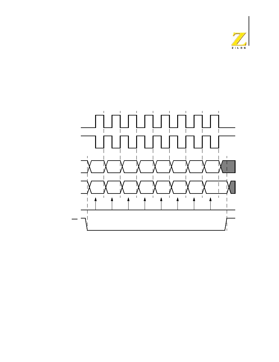
PS019915-1005
Serial
Peripheral
Interface
Z8 Encore!
�
64K Series
Product Specification
129
Transfer Format PHASE Equals Zero
Figure 25 illustrates the timing diagram for an SPI transfer in which PHASE is cleared to
0. The two SCK waveforms show polarity with CLKPOL reset to 0 and with CLKPOL set
to one. The diagram may be interpreted as either a Master or Slave timing diagram
because the SCK Master-In/Slave-Out (MISO) and Master-Out/Slave-In (MOSI) pins are
directly connected between the Master and the Slave.
Figure 25. SPI Timing When
PHASE
is 0
Transfer Format
PHASE
Equals One
Figure 26 illustrates the timing diagram for an SPI transfer in which PHASE is one. Two
waveforms are depicted for SCK, one for CLKPOL reset to 0 and another for CLKPOL set
to 1.
SCK
(CLKPOL = 0)
SCK
(CLKPOL = 1)
Bit7
Bit6
Bit5
Bit4
Bit3
Bit2
Bit1
Bit0
MOSI
Bit7
Bit6
Bit5
Bit4
Bit3
Bit2
Bit1
Bit0
MISO
Input Sample Time
SS
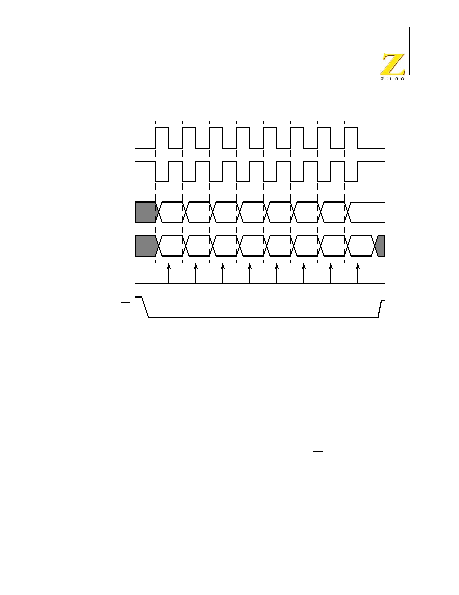
PS019915-1005
Serial
Peripheral
Interface
Z8 Encore!
�
64K Series
Product Specification
130
Figure 26. SPI Timing When
PHASE
is 1
Multi-Master Operation
In a multi-master SPI system, all SCK pins are tied together, all MOSI pins are tied
together and all MISO pins are tied together. All SPI pins must then be configured in
open-drain mode to prevent bus contention. At any one time, only one SPI device is con-
figured as the Master and all other SPI devices on the bus are configured as Slaves. The
Master enables a single Slave by asserting the SS pin on that Slave only. Then, the single
Master drives data out its SCK and MOSI pins to the SCK and MOSI pins on the Slaves
(including those which are not enabled). The enabled Slave drives data out its MISO pin to
the MISO Master pin.
For a Master device operating in a multi-master system, if the SS pin is configured as an
input and is driven Low by another Master, the COL bit is set to 1 in the SPI Status Regis-
ter. The COL bit indicates the occurrence of a multi-master collision (mode fault error con-
dition).
Slave Operation
The SPI block is configured for slave mode operation by setting the SPIEN bit to 1 and the
MMEN bit to 0 in the SPICTL register and setting the SSIO bit to 0 in the SPIMODE reg-
SCK
(CLKPOL = 0)
SCK
(CLKPOL = 1)
Bit7
Bit6
Bit5
Bit4
Bit3
Bit2
Bit1
Bit0
MOSI
Bit7
Bit6
Bit5
Bit4
Bit3
Bit2
Bit1
Bit0
MISO
Input Sample Time
SS

PS019915-1005
Serial
Peripheral
Interface
Z8 Encore!
�
64K Series
Product Specification
131
ister. The IRQE, PHASE, CLKPOL, WOR bits in the SPICTL register and the NUMBITS
field in the SPIMODE register must be set to be consistent with the other SPI devices. The
STR bit in the SPICTL register may be used if desired to force a "startup" interrupt. The
BIRQ bit in the SPICTL register and the SSV bit in the SPIMODE register are not used in
slave mode. The SPI baud rate generator is not used in slave mode so the SPIBRH and
SPIBRL registers need not be initialized.
If the slave has data to send to the master, the data must be written to the SPIDAT register
before the transaction starts (first edge of SCK when SS is asserted). If the SPIDAT regis-
ter is not written prior to the slave transaction, the MISO pin outputs whatever value is
currently in the SPIDAT register.
Due to the delay resulting from synchronization of the SPI input signals to the internal sys-
tem clock, the maximum SPICLK baud rate that can be supported in slave mode is the sys-
tem clock frequency (XIN) divided by 8. This rate is controlled by the SPI master.
Error Detection
The SPI contains error detection logic to support SPI communication protocols and recog-
nize when communication errors have occurred. The SPI Status register indicates when a
data transmission error has been detected.
Overrun (Write Collision)
An overrun error (write collision) indicates a write to the SPI Data register was attempted
while a data transfer is in progress (in either master or slave modes). An overrun sets the
OVR
bit in the SPI Status register to 1. Writing a 1 to OVR clears this error flag. The data
register is not altered when a write occurs while data transfer is in progress.
Mode Fault (Multi-Master Collision)
A mode fault indicates when more than one Master is trying to communicate at the same
time (a multi-master collision). The mode fault is detected when the enabled Master's SS
pin is asserted. A mode fault sets the COL bit in the SPI Status register to 1. Writing a 1 to
COL
clears this error flag.
Slave Mode Abort
In slave mode of operation if the SS pin deasserts before all bits in a character have been
transferred, the transaction is aborted. When this condition occurs the ABT bit is set in the
SPISTAT register as well as the IRQ bit (indicating the transaction is complete). The next
time SS asserts, the MISO pin outputs SPIDAT[7], regardless of where the previous trans-
action left off. Writing a 1 to ABT clears this error flag.
SPI Interrupts
When SPI interrupts are enabled, the SPI generates an interrupt after character transmis-
sion/reception completes in both master and slave modes. A character can be defined to be

PS019915-1005
Serial
Peripheral
Interface
Z8 Encore!
�
64K Series
Product Specification
132
1 through 8 bits by the NUMBITS field in the SPI Mode register. In slave mode it is not
necessary for SS to deassert between characters to generate the interrupt. The SPI in Slave
mode can also generate an interrupt if the SS signal deasserts prior to transfer of all the bits
in a character (see description of slave abort error above). Writing a 1 to the IRQ bit in the
SPI Status Register clears the pending SPI interrupt request. The IRQ bit must be cleared
to 0 by the Interrupt Service Routine to generate future interrupts. To start the transfer pro-
cess, an SPI interrupt may be forced by software writing a 1 to the STR bit in the SPICTL
register.
If the SPI is disabled, an SPI interrupt can be generated by a Baud Rate Generator time-
out. This timer function must be enabled by setting the BIRQ bit in the SPICTL register.
This Baud Rate Generator time-out does not set the IRQ bit in the SPISTAT register, just
the SPI interrupt bit in the interrupt controller.
SPI Baud Rate Generator
In SPI Master mode, the Baud Rate Generator creates a lower frequency serial clock
(SCK) for data transmission synchronization between the Master and the external Slave.
The input to the Baud Rate Generator is the system clock. The SPI Baud Rate High and
Low Byte registers combine to form a 16-bit reload value, BRG[15:0], for the SPI Baud
Rate Generator. The SPI baud rate is calculated using the following equation:
Minimum baud rate is obtained by setting BRG[15:0] to 0000H for a clock divisor value
of (2 X 65536 = 131072).
When the SPI is disabled, the Baud Rate Generator can function as a basic 16-bit timer
with interrupt on time-out. To configure the Baud Rate Generator as a timer with interrupt
on time-out, complete the following procedure:
1. Disable the SPI by clearing the SPIEN bit in the SPI Control register to 0.
2. Load the desired 16-bit count value into the SPI Baud Rate High and Low Byte
registers.
3. Enable the Baud Rate Generator timer function and associated interrupt by setting the
BIRQ
bit in the SPI Control register to 1.
When configured as a general purpose timer, the interrupt interval is calculated using the
following equation:
Interrupt Interval (s) = System Clock Period (s) �BRG[15:0]
]
SPI Baud Rate (bits/s)
System Clock Frequency (Hz)
2 BRG[15:0]
�
----------------------------------------------------------------------------
=
PS019915-1005
Serial
Peripheral
Interface
Z8 Encore!
�
64K Series
Product Specification
133
SPI Control Register Definitions
SPI Data Register
The SPI Data register (Table 62) stores both the outgoing (transmit) data and the incoming
(receive) data. Reads from the SPI Data register always return the current contents of the
8-bit shift register. Data is shifted out starting with bit 7. The last bit received resides in bit
position 0.
With the SPI configured as a Master, writing a data byte to this register initiates the data
transmission. With the SPI configured as a Slave, writing a data byte to this register loads
the shift register in preparation for the next data transfer with the external Master. In either
the Master or Slave modes, if a transmission is already in progress, writes to this register
are ignored and the Overrun error flag, OVR, is set in the SPI Status register.
When the character length is less than 8 bits (as set by the NUMBITS field in the SPI Mode
register), the transmit character must be left justified in the SPI Data register. A received
character of less than 8 bits is right justified (last bit received is in bit position 0). For
example, if the SPI is configured for 4-bit characters, the transmit characters must be writ-
ten to SPIDATA[7:4] and the received characters are read from SPIDATA[3:0].
DATA--Data
Transmit and/or receive data.
SPI Control Register
The SPI Control register (Table 63) configures the SPI for transmit and receive operations.
Table 62. SPI Data Register (SPIDATA)
BITS
7
6
5
4
3
2
1
0
FIELD
DATA
RESET
X
R/W
R/W
ADDR
F60H
PS019915-1005
Serial
Peripheral
Interface
Z8 Encore!
�
64K Series
Product Specification
134
IRQE--Interrupt Request Enable
0 = SPI interrupts are disabled. No interrupt requests are sent to the Interrupt Controller.
1 = SPI interrupts are enabled. Interrupt requests are sent to the Interrupt Controller.
STR--Start an SPI Interrupt Request
0 = No effect.
1 = Setting this bit to 1 also sets the IRQ bit in the SPI Status register to 1. Setting this bit
forces the SPI to send an interrupt request to the Interrupt Control. This bit can be used by
software for a function similar to transmit buffer empty in a UART. Writing a 1 to the
IRQ
bit in the SPI Status register clears this bit to 0.
BIRQ--BRG Timer Interrupt Request
If the SPI is enabled, this bit has no effect. If the SPI is disabled:
0 = The Baud Rate Generator timer function is disabled.
1 = The Baud Rate Generator timer function and time-out interrupt are enabled.
PHASE--Phase Select
Sets the phase relationship of the data to the clock. Refer to the SPI Clock Phase and
Polarity Control section for more information on operation of the PHASE bit.
CLKPOL--Clock Polarity
0 = SCK idles Low (0).
1 = SCK idle High (1).
WOR--Wire-OR (Open-Drain) Mode Enabled
0 = SPI signal pins not configured for open-drain.
1 = All four SPI signal pins (SCK, SS, MISO, MOSI) configured for open-drain function.
This setting is typically used for multi-master and/or multi-slave configurations.
MMEN--SPI Master Mode Enable
0 = SPI configured in Slave mode.
1 = SPI configured in Master mode.
SPIEN--SPI Enable
0 = SPI disabled.
1 = SPI enabled.
Table 63. SPI Control Register (SPICTL)
BITS
7
6
5
4
3
2
1
0
FIELD
IRQE
STR
BIRQ
PHASE
CLKPOL
WOR
MMEN
SPIEN
RESET
0
R/W
R/W
ADDR
F61H

PS019915-1005
Serial
Peripheral
Interface
Z8 Encore!
�
64K Series
Product Specification
135
SPI Status Register
The SPI Status register (Table 64) indicates the current state of the SPI. All bits revert to
their reset state if the SPIEN bit in the SPICTL register = 0.
IRQ--Interrupt Request
If SPIEN = 1, this bit is set if the STR bit in the SPICTL register is set, or upon completion
of an SPI master or slave transaction. This bit does not set if SPIEN = 0 and the SPI Baud
Rate Generator is used as a timer to generate the SPI interrupt.
0 = No SPI interrupt request pending.
1 = SPI interrupt request is pending.
OVR--Overrun
0 = An overrun error has not occurred.
1 = An overrun error has been detected.
COL--Collision
0 = A multi-master collision (mode fault) has not occurred.
1 = A multi-master collision (mode fault) has been detected.
ABT--Slave mode transaction abort
This bit is set if the SPI is configured in slave mode, a transaction is occurring and SS
deasserts before all bits of a character have been transferred as defined by the NUMBITS
field of the SPIMODE register. The IRQ bit also sets, indicating the transaction has com-
pleted.
0 = A slave mode transaction abort has not occurred.
1 = A slave mode transaction abort has been detected.
Reserved--Must be 0.
TXST--Transmit Status
0 = No data transmission currently in progress.
1 = Data transmission currently in progress.
Table 64. SPI Status Register (SPISTAT)
BITS
7
6
5
4
3
2
1
0
FIELD
IRQ
OVR
COL
ABT
Reserved
TXST
SLAS
RESET
0
1
R/W
R/W*
R
ADDR
F62H
R/W* = Read access. Write a 1 to clear the bit to 0.
PS019915-1005
Serial
Peripheral
Interface
Z8 Encore!
�
64K Series
Product Specification
136
SLAS--Slave Select
If SPI enabled as a Slave,
0 = SS input pin is asserted (Low)
1 = SS input is not asserted (High).
If SPI enabled as a Master, this bit is not applicable.
SPI Mode Register
The SPI Mode register (Table 65) configures the character bit width and the direction and
value of the SS pin.
Reserved--Must be 0.
DIAG - Diagnostic Mode Control bit
This bit is for SPI diagnostics. Setting this bit allows the Baud Rate Generator value to be
read using the SPIBRH and SPIBRL register locations.
0 = Reading SPIBRH, SPIBRL returns the value in the SPIBRH and SPIBRL registers
1 = Reading SPIBRH returns bits [15:8] of the SPI Baud Rate Generator; and reading SPI-
BRL returns bits [7:0] of the SPI Baud Rate Counter. The Baud Rate Counter High and
Low byte values are not buffered.
Exercise caution if reading the values while the BRG is counting.
NUMBITS[2:0]--Number of Data Bits Per Character to Transfer
This field contains the number of bits to shift for each character transfer. Refer to the SPI
Data Register description for information on valid bit positions when the character length
is less than 8-bits.
000 = 8 bits
001 = 1 bit
010 = 2 bits
011 = 3 bits
100 = 4 bits
101 = 5 bits
Table 65. SPI Mode Register (SPIMODE)
BITS
7
6
5
4
3
2
1
0
FIELD
Reserved
DIAG
NUMBITS[2:0]
SSIO
SSV
RESET
0
R/W
R
R/W
ADDR
F63H
Caution:
PS019915-1005
Serial
Peripheral
Interface
Z8 Encore!
�
64K Series
Product Specification
137
110 = 6 bits
111 = 7 bits.
SSIO--Slave Select I/O
0 = SS pin configured as an input.
1 = SS pin configured as an output (Master mode only).
SSV--Slave Select Value
If SSIO = 1 and SPI configured as a Master:
0 = SS pin driven Low (0).
1 = SS pin driven High (1).
This bit has no effect if SSIO = 0 or SPI configured as a Slave.
SPI Diagnostic State Register
The SPI Diagnostic State register (Table 66) provides observability of internal state. This
is a read only register used for SPI diagnostics.
SCKEN - Shift Clock Enable
0 = The internal Shift Clock Enable signal is deasserted
1 = The internal Shift Clock Enable signal is asserted (shift register is updates on next sys-
tem clock)
TCKEN - Transmit Clock Enable
0 = The internal Transmit Clock Enable signal is deasserted.
1 = The internal Transmit Clock Enable signal is asserted. When this is asserted the serial
data out is updated on the next system clock (MOSI or MISO).
SPISTATE - SPI State Machine
Defines the current state of the internal SPI State Machine.
Table 66. SPI Diagnostic State Register (SPIDST)
BITS
7
6
5
4
3
2
1
0
FIELD
SCKEN
TCKEN
SPISTATE
RESET
0
R/W
R
ADDR
F64H
PS019915-1005
Serial
Peripheral
Interface
Z8 Encore!
�
64K Series
Product Specification
138
SPI Baud Rate High and Low Byte Registers
The SPI Baud Rate High and Low Byte registers (Tables 67 and 68) combine to form a 16-
bit reload value, BRG[15:0], for the SPI Baud Rate Generator.
When congured as a general purpose timer, the SPI BRG interrupt interval is calculated
using the following equation:
SPI BRG Interrupt Interval (s) = System Clock Period (s) �BRG[15:0]
].
BRH = SPI Baud Rate High Byte
Most significant byte, BRG[15:8], of the SPI Baud Rate Generator's reload value.
BRL = SPI Baud Rate Low Byte
Least significant byte, BRG[7:0], of the SPI Baud Rate Generator's reload value.
Table 67. SPI Baud Rate High Byte Register (SPIBRH)
BITS
7
6
5
4
3
2
1
0
FIELD
BRH
RESET
1
R/W
R/W
ADDR
F66H
Table 68. SPI Baud Rate Low Byte Register (SPIBRL)
BITS
7
6
5
4
3
2
1
0
FIELD
BRL
RESET
1
R/W
R/W
ADDR
F67H

Z8 Encore!
�
64K Series
Product Specification
PS019915-1005
I2C
Controller
139
I
2
C Controller
Overview
The I
2
C Controller makes the 64K Series products bus-compatible with the I
2
C
TM
proto-
col. The I
2
C Controller consists of two bidirectional bus lines--a serial data signal (SDA)
and a serial clock signal (SCL). Features of the I
2
C Controller include:
�
Transmit and Receive Operation in MASTER mode
�
Maximum data rate of 400kbit/sec
�
7- and 10-bit addressing modes for Slaves
�
Unrestricted number of data bytes transmitted per transfer
The I
2
C Controller in the 64K Series products does not operate in Slave mode.
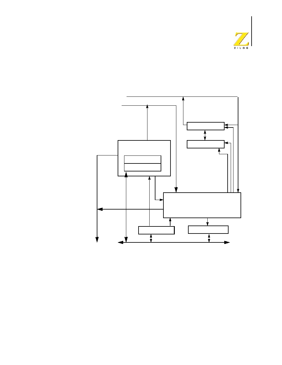
PS019915-1005
I2C
Controller
Z8 Encore!
�
64K Series
Product Specification
140
Architecture
Figure 27 illustrates the architecture of the I
2
C Controller.
Operation
The I
2
C Controller operates in MASTER mode to transmit and receive data. Only a single
master is supported. Arbitration between two masters must be accomplished in software.
I
2
C supports the following operations:
�
Master transmits to a 7-bit slave
�
Master transmits to a 10-bit slave
Figure 27. I
2
C Controller Block Diagram
SDA
SCL
I
2
CCTL
ISHIFT
I
2
CDATA
I
2
CBRH
I
2
CBRL
Shift
Load
Tx/Rx State Machine
Baud Rate Generator
Receive
I
2
CSTAT
Register Bus
I
2
C Interrupt

PS019915-1005
I2C
Controller
Z8 Encore!
�
64K Series
Product Specification
141
�
Master receives from a 7-bit slave
�
Master receives from a 10-bit slave
SDA and SCL Signals
I
2
C sends all addresses, data and acknowledge signals over the SDA line, most-significant
bit first. SCL is the common clock for the I
2
C Controller. When the SDA and SCL pin
alternate functions are selected for their respective GPIO ports, the pins are automatically
configured for open-drain operation.
The master (I
2
C) is responsible for driving the SCL clock signal, although the clock signal
can become skewed by a slow slave device. During the low period of the clock, the slave
pulls the SCL signal Low to suspend the transaction. The master releases the clock at the
end of the low period and notices that the clock remains low instead of returning to a high
level. When the slave releases the clock, the I
2
C Controller continues the transaction. All
data is transferred in bytes and there is no limit to the amount of data transferred in one
operation. When transmitting data or acknowledging read data from the slave, the SDA
signal changes in the middle of the low period of SCL and is sampled in the middle of the
high period of SCL.
I
2
C Interrupts
The I
2
C Controller contains four sources of interrupts--Transmit, Receive, Not Acknowl-
edge and baud rate generator. These four interrupt sources are combined into a single
interrupt request signal to the Interrupt Controller. The Transmit interrupt is enabled by the
IEN and TXI bits of the Control register. The Receive and Not Acknowledge interrupts are
enabled by the IEN bit of the Control register. The baud rate generator interrupt is enabled
by the BIRQ and IEN bits of the Control register.
Not Acknowledge interrupts occur when a Not Acknowledge condition is received from
the slave or sent by the I
2
C Controller and neither the
START
or
STOP
bit is set. The Not
Acknowledge event sets the NCKI bit of the I
2
C Status register and can only be cleared by
setting the
START
or
STOP
bit in the I
2
C Control register. When this interrupt occurs, the
I
2
C Controller waits until either the STOP or START bit is set before performing any
action. In an interrupt service routine, the NCKI bit should always be checked prior to ser-
vicing transmit or receive interrupt conditions because it indicates the transaction is being
terminated.
Receive interrupts occur when a byte of data has been received by the I
2
C Controller
(master reading data from slave). This procedure sets the RDRF bit of the I
2
C Status regis-
ter. The RDRF bit is cleared by reading the I
2
C Data register. The RDRF bit is set during
the acknowledge phase. The I
2
C Controller pauses after the acknowledge phase until the
receive interrupt is cleared before performing any other action.

PS019915-1005
I2C
Controller
Z8 Encore!
�
64K Series
Product Specification
142
Transmit interrupts occur when the TDRE bit of the I
2
C Status register sets and the TXI
bit in the I
2
C Control register is set. Transmit interrupts occur under the following condi-
tions when the transmit data register is empty:
�
The I
2
C Controller is enabled
�
The first bit of the byte of an address is shifting out and the RD bit of the I
2
C Status
register is deasserted.
�
The first bit of a 10-bit address shifts out.
�
The first bit of write data shifts out.
Writing to the I
2
C Data register always clears the TRDE bit to 0. When TDRE is asserted,
the I2C Controller pauses at the beginning of the Acknowledge cycle of the byte currently
shifting out until the Data register is written with the next value to send or the STOP or
START bits are set indicating the current byte is the last one to send.
The fourth interrupt source is the baud rate generator. If the I2C Controller is disabled
(IEN bit in the I2CCTL register = 0) and the BIRQ bit in the I2CCTL register = 1, an inter-
rupt is generated when the baud rate generator counts down to 1. This allows the I
2
C baud
rate generator to be used by software as a general purpose timer when IEN = 0.
Software Control of I
2
C Transactions
Software can control I
2
C transactions by using the I
2
C Controller interrupt, by polling the
I
2
C Status register or by DMA. Note that not all products include a DMA Controller.
To use interrupts, the I
2
C interrupt must be enabled in the Interrupt Controller. The TXI bit
in the I
2
C Control register must be set to enable transmit interrupts.
To control transactions by polling, the interrupt bits (TDRE, RDRF and NCKI) in the I
2
C
Status register should be polled. The TDRE bit asserts regardless of the state of the TXI
bit.
Either or both transmit and receive data movement can be controlled by the DMA Control-
ler. The DMA Controller channel(s) must be initialized to select the I
2
C transmit and
receive requests. Transmit DMA requests require that the TXI bit in the I
2
C Control regis-
ter be set.
A transmit (write) DMA operation hangs if the slave responds with a Not
Acknowledge before the last byte has been sent. After receiving the Not
Acknowledge, the I
2
C Controller sets the NCKI bit in the Status register
and pauses until either the STOP or START bits in the Control register are
set.
Note:
Caution:

PS019915-1005
I2C
Controller
Z8 Encore!
�
64K Series
Product Specification
143
In order for a receive (read) DMA transaction to send a Not Acknowledge
on the last byte, the receive DMA must be set up to receive n-1 bytes, then
software must set the NAK bit and receive the last (nth) byte directly.
Start and Stop Conditions
The master (I
2
C) drives all Start and Stop signals and initiates all transactions. To start a
transaction, the I
2
C Controller generates a START condition by pulling the SDA signal
Low while SCL is High. To complete a transaction, the I
2
C Controller generates a Stop
condition by creating a low-to-high transition of the SDA signal while the SCL signal is
high. The START and STOP bits in the I
2
C Control register control the sending of the
Start and Stop conditions. A master is also allowed to end one transaction and begin a new
one by issuing a Restart. This is accomplished by setting the START bit at the end of a
transaction, rather than the STOP bit. Note that the Start condition not sent until the
START bit is set and data has been written to the I
2
C Data register.
Master Write and Read Transactions
The following sections provide a recommended procedure for performing I
2
C write and
read transactions from the I
2
C Controller (master) to slave I
2
C devices. In general soft-
ware should rely on the TDRE, RDRF and NCKI bits of the status register (these bits gen-
erate interrupts) to initiate software actions. When using interrupts or DMA, the TXI bit is
set to start each transaction and cleared at the end of each transaction to eliminate a "trail-
ing" Transmit interrupt.
Caution should be used in using the ACK status bit within a transaction because it is diffi-
cult for software to tell when it is updated by hardware.
When writing data to a slave, the I
2
C pauses at the beginning of the Acknowledge cycle if
the data register has not been written with the next value to be sent (TDRE bit in the I
2
C
Status register = 1). In this scenario where software is not keeping up with the I
2
C bus
(TDRE asserted longer than one byte time), the Acknowledge clock cycle for byte n is
delayed until the Data register is written with byte n + 1, and appears to be grouped with
the data clock cycles for byte n+1. If either the START or STOP bit is set, the I
2
C does not
pause prior to the Acknowledge cycle because no additional data is sent.
When a Not Acknowledge condition is received during a write (either during the address
or data phases), the I
2
C Controller generates the Not Acknowledge interrupt (NCKI = 1)
and pause until either the STOP or START bit is set. Unless the Not Acknowledge was
received on the last byte, the Data register will already have been written with the next
address or data byte to send. In this case the FLUSH bit of the Control register should be
set at the same time the STOP or START bit is set to remove the stale transmit data and
enable subsequent Transmit interrupts.
When reading data from the slave, the I
2
C pauses after the data Acknowledge cycle until
the receive interrupt is serviced and the RDRF bit of the status register is cleared by read-

PS019915-1005
I2C
Controller
Z8 Encore!
�
64K Series
Product Specification
144
ing the I
2
C Data register. Once the I
2
C data register has been read, the I
2
C reads the next
data byte.
Address Only Transaction with a 7-bit Address
In the situation where software determines if a slave with a 7-bit address is responding
without sending or receiving data, a transaction can be done which only consists of an
address phase. Figure 28 illustrates this "address only" transaction to determine if a slave
with a 7-bit address will acknowledge. As an example, this transaction can be used after a
"write" has been done to a EEPROM to determine when the EEPROM completes its inter-
nal write operation and is once again responding to I
2
C transactions. If the slave does not
Acknowledge, the transaction can be repeated until the slave does Acknowledge.
Figure 28. 7-Bit Address Only Transaction Format
The procedure for an address only transaction to a 7-bit addressed slave is as follows:
1. Software asserts the IEN bit in the I
2
C Control register.
2. Software asserts the TXI bit of the I
2
C Control register to enable Transmit interrupts.
3. The I
2
C interrupt asserts, because the I
2
C Data register is empty (TDRE = 1)
4. Software responds to the TDRE bit by writing a 7-bit slave address plus write bit (=0)
to the I
2
C Data register. As an alternative this could be a read operation instead of a
write operation.
5. Software sets the START and STOP bits of the I
2
C Control register and clears the TXI
bit.
6. The I
2
C Controller sends the START condition to the I
2
C slave.
7. The I
2
C Controller loads the I
2
C Shift register with the contents of the I
2
C Data
register.
8. Software polls the STOP bit of the I2C Control register. Hardware deasserts the STOP
bit when the address only transaction is completed.
9. Software checks the ACK bit of the I2C Status register. If the slave acknowledged,
the ACK bit is = 1. If the slave does not acknowledge, the ACK bit is = 0. The NCKI
interrupt does not occur in the not acknowledge case because the STOP bit was set.
S
Slave Address W = 0 A/A
P

PS019915-1005
I2C
Controller
Z8 Encore!
�
64K Series
Product Specification
145
Write Transaction with a 7-Bit Address
Figure 29 illustrates the data transfer format for a 7-bit addressed slave. Shaded regions
indicate data transferred from the I
2
C Controller to slaves and unshaded regions indicate
data transferred from the slaves to the I
2
C Controller.
Figure 29. 7-Bit Addressed Slave Data Transfer Format
The procedure for a transmit operation to a 7-bit addressed slave is as follows:
1. Software asserts the IEN bit in the I
2
C Control register.
2. Software asserts the TXI bit of the I
2
C Control register to enable Transmit interrupts.
3. The I
2
C interrupt asserts, because the I
2
C Data register is empty
4. Software responds to the TDRE bit by writing a 7-bit slave address plus write bit (=0)
to the I
2
C Data register.
5. Software asserts the START bit of the I
2
C Control register.
6. The I
2
C Controller sends the START condition to the I
2
C slave.
7. The I
2
C Controller loads the I
2
C Shift register with the contents of the I
2
C Data
register.
8. After one bit of address has been shifted out by the SDA signal, the Transmit interrupt
is asserted (TDRE = 1).
9. Software responds by writing the transmit data into the I
2
C Data register.
10. The I
2
C Controller shifts the rest of the address and write bit out by the SDA signal.
11. If the I
2
C slave sends an acknowledge (by pulling the SDA signal low) during the next
high period of SCL the I
2
C Controller sets the ACK bit in the I
2
C Status register.
Continue with step 12.
If the slave does not acknowledge, the Not Acknowledge interrupt occurs (NCKI bit is
set in the Status register, ACK bit is cleared). Software responds to the Not
Acknowledge interrupt by setting the STOP and FLUSH bits and clearing the TXI bit.
The I2C Controller sends the STOP condition on the bus and clears the STOP and
NCKI bits. The transaction is complete (ignore following steps).
12. The I
2
C Controller loads the contents of the I
2
C Shift register with the contents of the
I
2
C Data register.
S
Slave Address W = 0
A
Data
A
Data
A
Data
A/A P/S

PS019915-1005
I2C
Controller
Z8 Encore!
�
64K Series
Product Specification
146
13. The I
2
C Controller shifts the data out of using the SDA signal. After the first bit is
sent, the Transmit interrupt is asserted.
14. If more bytes remain to be sent, return to step 9.
15. Software responds by setting the STOP bit of the I
2
C Control register (or START bit
to initiate a new transaction). In the STOP case, software clears the TXI bit of the I
2
C
Control register at the same time.
16. The I
2
C Controller completes transmission of the data on the SDA signal.
17. The slave may either Acknowledge or Not Acknowledge the last byte. Because either
the STOP or START bit is already set, the NCKI interrupt does not occur.
18. The I
2
C Controller sends the STOP (or RESTART) condition to the I
2
C bus. The
STOP or START bit is cleared.
Address Only Transaction with a 10-bit Address
In the situation where software wants to determine if a slave with a 10-bit address is
responding without sending or receiving data, a transaction can be done which only con-
sists of an address phase. Figure 30 illustrates this "address only" transaction to determine
if a slave with 10-bit address will acknowledge. As an example, this transaction can be
used after a "write" has been done to a EEPROM to determine when the EEPROM com-
pletes its internal write operation and is once again responding to I2C transactions. If the
slave does not Acknowledge the transaction can be repeated until the slave is able to
Acknowledge.
Figure 30. 10-Bit Address Only Transaction Format
The procedure for an address only transaction to a 10-bit addressed slave is as follows:
1. Software asserts the IEN bit in the I
2
C Control register.
2. Software asserts the TXI bit of the I
2
C Control register to enable Transmit interrupts.
3. The I
2
C interrupt asserts, because the I
2
C Data register is empty (TDRE = 1)
4. Software responds to the TDRE interrupt by writing the first slave address byte. The
least-significant bit must be 0 for the write operation.
5. Software asserts the START bit of the I
2
C Control register.
6. The I
2
C Controller sends the START condition to the I
2
C slave.
S
Slave Address
1st 7 bits
W = 0 A/A
Slave Address
2nd Byte
A/A P

PS019915-1005
I2C
Controller
Z8 Encore!
�
64K Series
Product Specification
147
7. The I
2
C Controller loads the I
2
C Shift register with the contents of the I
2
C Data
register.
8. After one bit of address is shifted out by the SDA signal, the Transmit interrupt is
asserted.
9. Software responds by writing the second byte of address into the contents of the I
2
C
Data register.
10. The I
2
C Controller shifts the rest of the first byte of address and write bit out the SDA
signal.
11. If the I
2
C slave sends an acknowledge by pulling the SDA signal low during the next
high period of SCL the I
2
C Controller sets the ACK bit in the I
2
C Status register.
Continue with step 12.
If the slave does not acknowledge the first address byte, the I
2
C Controller sets the
NCKI
bit and clears the ACK bit in the I
2
C Status register. Software respons to the
Not Acknowledge interrupt by setting the STOP and FLUSH bits and clearing the TXI
bit. The I2C Controller sends the STOP condition on the bus and clears the STOP and
NCKI bits. The transaction is complete (ignore following steps).
12. The I
2
C Controller loads the I
2
C Shift register with the contents of the I
2
C Data
register (2nd byte of address).
13. The I
2
C Controller shifts the second address byte out the SDA signal. After the first
bit has been sent, the Transmit interrupt is asserted.
14. Software responds by setting the STOP bit in the I2C Control register. The TXI bit can
be cleared at the same time.
15. Software polls the STOP bit of the I
2
C Control register. Hardware deasserts the STOP
bit when the transaction is completed (STOP condition has been sent).
16. Software checks the ACK bit of the I
2
C Status register. If the slave acknowledged, the
ACK bit is = 1. If the slave does not acknowledge, the ACK bit is = 0. The NCKI
interrupt do not occur because the STOP bit was set.
Write Transaction with a 10-Bit Address
Figure 31 illustrates the data transfer format for a 10-bit addressed slave. Shaded regions
indicate data transferred from the I
2
C Controller to slaves and unshaded regions indicate
data transferred from the slaves to the I
2
C Controller.
Figure 31. 10-Bit Addressed Slave Data Transfer Format
S
Slave Address
1st 7 bits
W = 0 A
Slave Address
2nd Byte
A Data A Data A/A P/S

PS019915-1005
I2C
Controller
Z8 Encore!
�
64K Series
Product Specification
148
The first seven bits transmitted in the first byte are
11110XX
. The two bits
XX
are the two
most-significant bits of the 10-bit address. The lowest bit of the first byte transferred is the
read/write control bit (=0). The transmit operation is carried out in the same manner as 7-
bit addressing.
The procedure for a transmit operation on a 10-bit addressed slave is as follows:
1. Software asserts the IEN bit in the I
2
C Control register.
2. Software asserts the TXI bit of the I
2
C Control register to enable Transmit interrupts.
3. The I
2
C interrupt asserts because the I
2
C Data register is empty.
4. Software responds to the TDRE interrupt by writing the first slave address byte to the
I
2
C Data register. The least-significant bit must be 0 for the write operation.
5. Software asserts the START bit of the I
2
C Control register.
6. The I
2
C Controller sends the START condition to the I
2
C slave.
7. The I
2
C Controller loads the I
2
C Shift register with the contents of the I
2
C Data
register.
8. After one bit of address is shifted out by the SDA signal, the Transmit interrupt is
asserted.
9. Software responds by writing the second byte of address into the contents of the I
2
C
Data register.
10. The I
2
C Controller shifts the rest of the first byte of address and write bit out the SDA
signal.
11. If the I
2
C slave acknowledges the first address byte by pulling the SDA signal low
during the next high period of SCL, the I
2
C Controller sets the ACK bit in the I
2
C
Status register. Continue with step 12.
If the slave does not acknowledge the first address byte, the I
2
C Controller sets the
NCKI
bit and clears the ACK bit in the I
2
C Status register. Software responds to the
Not Acknowledge interrupt by setting the STOP and FLUSH bits and clearing the TXI
bit. The I2C Controller sends the STOP condition on the bus and clears the STOP and
NCKI bits. The transaction is complete (ignore the following steps).
12. The I
2
C Controller loads the I
2
C Shift register with the contents of the I
2
C Data
register.
13. The I
2
C Controller shifts the second address byte out the SDA signal. After the first
bit has been sent, the Transmit interrupt is asserted.
14. Software responds by writing a data byte to the I
2
C Data register.
15. The I
2
C Controller completes shifting the contents of the shift register on the SDA
signal.

PS019915-1005
I2C
Controller
Z8 Encore!
�
64K Series
Product Specification
149
16. If the I
2
C slave sends an acknowledge by pulling the SDA signal low during the next
high period of SCL, the I
2
C Controller sets the ACK bit in the I
2
C Status register.
Continue with step 17.
If the slave does not acknowledge the second address byte or one of the data bytes, the
I
2
C Controller sets the NCKI bit and clears the ACK bit in the I
2
C Status register.
Software responds to the Not Acknowledge interrupt by setting the STOP and FLUSH
bits and clearing the TXI bit. The I2C Controller sends the STOP condition on the bus
and clears the STOP and NCKI bits. The transaction is complete (ignore the following
steps).
17. The I
2
C Controller shifts the data out by the SDA signal. After the first bit is sent, the
Transmit interrupt is asserted.
18. If more bytes remain to be sent, return to step 14.
19. If the last byte is currently being sent, software sets the STOP bit of the I
2
C Control
register (or START bit to initiate a new transaction). In the STOP case, software also
clears the TXI bit of the I
2
C Control register at the same time.
20. The I
2
C Controller completes transmission of the last data byte on the SDA signal.
21. The slave may either Acknowledge or Not Acknowledge the last byte. Because either
the STOP or START bit is already set, the NCKI interrupt does not occur.
22. The I
2
C Controller sends the STOP (or RESTART) condition to the I
2
C bus and clears
the STOP (or START) bit.
Read Transaction with a 7-Bit Address
Figure 32 illustrates the data transfer format for a read operation to a 7-bit addressed slave.
The shaded regions indicate data transferred from the I
2
C Controller to slaves and
unshaded regions indicate data transferred from the slaves to the I
2
C Controller.
Figure 32. Receive Data Transfer Format for a 7-Bit Addressed Slave
The procedure for a read operation to a 7-bit addressed slave is as follows:
1. Software writes the I
2
C Data register with a 7-bit slave address plus the read bit (=1).
2. Software asserts the START bit of the I
2
C Control register.
3. If this is a single byte transfer, Software asserts the NAK bit of the I
2
C Control register
so that after the first byte of data has been read by the I
2
C Controller, a Not
Acknowledge is sent to the I
2
C slave.
S
Slave Address
R = 1
A
Data
A
Data
A
P/S

PS019915-1005
I2C
Controller
Z8 Encore!
�
64K Series
Product Specification
150
4. The I
2
C Controller sends the START condition.
5. The I
2
C Controller shifts the address and read bit out the SDA signal.
6. If the I
2
C slave acknowledges the address by pulling the SDA signal Low during the
next high period of SCL, the I
2
C Controller sets the ACK bit in the I
2
C Status register.
Continue with step 7.
If the slave does not acknowledge, the Not Acknowledge interrupt occurs (NCKI bit is
set in the Status register, ACK bit is cleared). Software responds to the Not
Acknowledge interrupt by setting the STOP bit and clearing the TXI bit. The I2C
Controller sends the STOP condition on the bus and clears the STOP and NCKI bits.
The transaction is complete (ignore the following steps).
7. The I
2
C Controller shifts in the byte of data from the I
2
C slave on the SDA signal. The
I
2
C Controller sends a Not Acknowledge to the I
2
C slave if the NAK bit is set (last
byte), else it sends an Acknowledge.
8. The I
2
C Controller asserts the Receive interrupt (RDRF bit set in the Status register).
9. Software responds by reading the I
2
C Data register which clears the RDRF bit. If there
is only one more byte to receive, set the NAK bit of the I
2
C Control register.
10. If there are more bytes to transfer, return to step 7.
11. After the last byte is shifted in, a Not Acknowledge interrupt is generated by the I
2
C
Controller.
12. Software responds by setting the STOP bit of the I
2
C Control register.
13. A STOP condition is sent to the I
2
C slave, the STOP and NCKI bits are cleared.
Read Transaction with a 10-Bit Address
Figure 33 illustrates the read transaction format for a 10-bit addressed slave. The shaded
regions indicate data transferred from the I
2
C Controller to slaves and unshaded regions
indicate data transferred from the slaves to the I
2
C Controller.
Figure 33. Receive Data Format for a 10-Bit Addressed Slave
The first seven bits transmitted in the first byte are
11110XX
. The two bits
XX
are the two
most-significant bits of the 10-bit address. The lowest bit of the first byte transferred is the
write control bit.
The data transfer procedure for a read operation to a 10-bit addressed slave is as follows:
S
Slave Address
1st 7 bits
W=0 A
Slave Address
2nd Byte
A S
Slave Address
1st 7 bits
R=1 A Data A Data A P

PS019915-1005
I2C
Controller
Z8 Encore!
�
64K Series
Product Specification
151
1. Software writes
11110B
followed by the two address bits and a 0 (write) to the I2C
Data register.
2. Software asserts the START and TXI bits of the I
2
C Control register.
3. The I
2
C Controller sends the Start condition.
4. The I
2
C Controller loads the I
2
C Shift register with the contents of the I
2
C Data
register.
5. After the first bit has been shifted out, a Transmit interrupt is asserted.
6. Software responds by writing the lower eight bits of address to the I
2
C Data register.
7. The I
2
C Controller completes shifting of the two address bits and a 0 (write).
8. If the I
2
C slave acknowledges the first address byte by pulling the SDA signal low
during the next high period of SCL, the I
2
C Controller sets the ACK bit in the I
2
C
Status register. Continue with step 9.
If the slave does not acknowledge the first address byte, the I
2
C Controller sets the
NCKI
bit and clears the ACK bit in the I
2
C Status register. Software responds to the
Not Acknowledge interrupt by setting the STOP and FLUSH bits and clearing the TXI
bit. The I2C Controller sends the STOP condition on the bus and clears the STOP and
NCKI bits. The transaction is complete (ignore following steps).
9. The I
2
C Controller loads the I
2
C Shift register with the contents of the I
2
C Data
register (second address byte).
10. The I
2
C Controller shifts out the second address byte. After the first bit is shifted, the
I
2
C Controller generates a Transmit interrupt.
11. Software responds by setting the START bit of the I
2
C Control register to generate a
repeated START and by clearing the TXI bit.
12. Software responds by writing 11110B followed by the 2-bit slave address and a 1
(read) to the I2C Data register.
13. If only one byte is to be read, software sets the NAK bit of the I
2
C Control register.
14. After the I
2
C Controller shifts out the 2nd address byte, the I
2
C slave sends an
acknowledge by pulling the SDA signal low during the next high period of SCL, the
I
2
C Controller sets the ACK bit in the I
2
C Status register. Continue with step 15.
If the slave does not acknowledge the second address byte, the I
2
C Controller sets the
NCKI
bit and clears the ACK bit in the I
2
C Status register. Software responds to the
Not Acknowledge interrupt by setting the STOP and FLUSH bits and clearing the TXI
bit. The I2C Controller sends the STOP condition on the bus and clears the STOP and
NCKI bits. The transaction is complete (ignore the following steps).
15. The I
2
C Controller sends the repeated START condition.

PS019915-1005
I2C
Controller
Z8 Encore!
�
64K Series
Product Specification
152
16. The I
2
C Controller loads the I
2
C Shift register with the contents of the I
2
C Data
register (third address transfer).
17. The I
2
C Controller sends
11110B
followed by the two most significant bits of the
slave read address and a 1 (read).
18. The I
2
C slave sends an acknowledge by pulling the SDA signal Low during the next
high period of SCL
If the slave were to Not Acknowledge at this point (this should not happen because the
slave did acknowledge the first two address bytes), software would respond by setting
the STOP and FLUSH bits and clearing the TXI bit. The I2C Controller sends the
STOP condition on the bus and clears the STOP and NCKI bits. The transaction is
complete (ignore the following steps).
19. The I
2
C Controller shifts in a byte of data from the I
2
C slave on the SDA signal. The
I
2
C Controller sends a Not Acknowledge to the I
2
C slave if the NAK bit is set (last
byte), else it sends an Acknowledge.
20. The I
2
C Controller asserts the Receive interrupt (RDRF bit set in the Status register).
21. Software responds by reading the I
2
C Data register which clears the RDRF bit. If there
is only one more byte to receive, set the NAK bit of the I
2
C Control register.
22. If there are one or more bytes to transfer, return to step 19.
23. After the last byte is shifted in, a Not Acknowledge interrupt is generated by the I
2
C
Controller.
24. Software responds by setting the STOP bit of the I
2
C Control register.
25. A STOP condition is sent to the I
2
C slave and the STOP and NCKI bits are cleared.
I
2
C Control Register Definitions
I
2
C Data Register
The I
2
C Data register (Table 69) holds the data that is to be loaded into the I
2
C Shift regis-
ter during a write to a slave. This register also holds data that is loaded from the I
2
C Shift
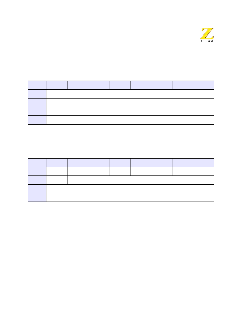
PS019915-1005
I2C
Controller
Z8 Encore!
�
64K Series
Product Specification
153
register during a read from a slave. The I
2
C Shift Register is not accessible in the Register
File address space, but is used only to buffer incoming and outgoing data.
I
2
C Status Register
The Read-only I
2
C Status register (Table 70) indicates the status of the I
2
C Controller.
TDRE--Transmit Data Register Empty
When the I
2
C Controller is enabled, this bit is 1 when the I
2
C Data register is empty.
When this bit is set, an interrupt is generated if the TXI bit is set, except when the I
2
C
Controller is shifting in data during the reception of a byte or when shifting an address and
the RD bit is set. This bit is cleared by writing to the I2CDATA register.
RDRF--Receive Data Register Full
This bit is set = 1 when the I
2
C Controller is enabled and the I
2
C Controller has received a
byte of data. When asserted, this bit causes the I
2
C Controller to generate an interrupt.
This bit is cleared by reading the I
2
C Data register (unless the read is performed using exe-
cution of the On-Chip Debugger's Read Register command).
ACK--Acknowledge
This bit indicates the status of the Acknowledge for the last byte transmitted or received.
When set, this bit indicates that an Acknowledge occurred for the last byte transmitted or
received. This bit is cleared when IEN = 0 or when a Not Acknowledge occurred for the
Table 69. I
2
C Data Register (I2CDATA)
BITS
7
6
5
4
3
2
1
0
FIELD
DATA
RESET
0
R/W
R/W
ADDR
F50H
Table 70. I
2
C Status Register (I2CSTAT)
BITS
7
6
5
4
3
2
1
0
FIELD
TDRE
RDRF
ACK
10B
RD
TAS
DSS
NCKI
RESET
1
0
R/W
R
ADDR
F51H

PS019915-1005
I2C
Controller
Z8 Encore!
�
64K Series
Product Specification
154
last byte transmitted or received. It is not reset at the beginning of each transaction and is
not reset when this register is read.
Software must be cautious in making decisions based on this bit within a
transaction because software cannot tell when the bit is updated by hard-
ware. In the case of write transactions, the I2C pauses at the beginning of
the Acknowledge cycle if the next transmit data or address byte has not
been written (TDRE = 1) and STOP and START = 0. In this case the ACK
bit is not updated until the transmit interrupt is serviced and the Acknowl-
edge cycle for the previous byte completes. Refer to Address Only Trans-
action with a 7-bit Address on page 144 and Address Only Transaction
with a 10-bit Address on page 146 for examples of how the ACK bit can
be used.
10B--10-Bit Address
This bit indicates whether a 10- or 7-bit address is being transmitted. After the START bit
is set, if the five most-significant bits of the address are 11110B, this bit is set. When set,
it is reset once the first byte of the address has been sent.
RD--Read
This bit indicates the direction of transfer of the data. It is active high during a read. The
status of this bit is determined by the least-significant bit of the I
2
C Shift register after the
START
bit is set.
TAS--Transmit Address State
This bit is active high while the address is being shifted out of the I
2
C Shift register.
DSS--Data Shift State
This bit is active high while data is being shifted to or from the I
2
C Shift register.
NCKI--NACK Interrupt
This bit is set high when a Not Acknowledge condition is received or sent and neither the
START nor the STOP bit is active. When set, this bit generates an interrupt that can only
be cleared by setting the START or STOP bit, allowing the user to specify whether he
wants to perform a STOP or a repeated START.
Caution:
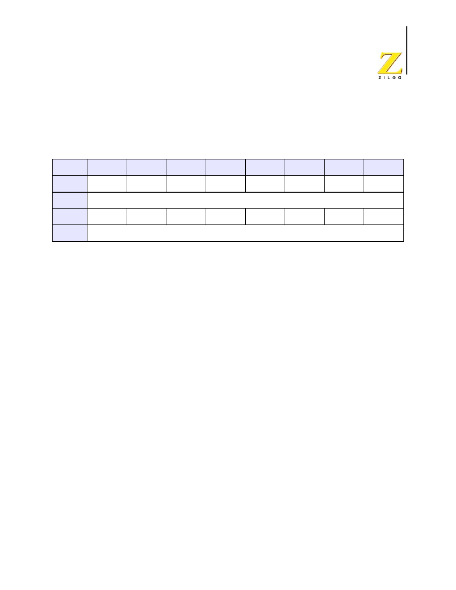
PS019915-1005
I2C
Controller
Z8 Encore!
�
64K Series
Product Specification
155
I
2
C Control Register
The I
2
C Control register (Table 71) enables the I
2
C operation.
IEN--I
2
C Enable
1 = The I
2
C transmitter and receiver are enabled.
0 = The I
2
C transmitter and receiver are disabled.
START--Send Start Condition
This bit sends the Start condition. Once asserted, it is cleared by the I
2
C Controller after it
sends the START condition or if the IEN bit is deasserted. If this bit is 1, it cannot be
cleared to 0 by writing to the register. After this bit is set, the Start condition is sent if there
is data in the I
2
C Data or I
2
C Shift register. If there is no data in one of these registers, the
I
2
C Controller waits until the Data register is written. If this bit is set while the I
2
C Con-
troller is shifting out data, it generates a START condition after the byte shifts and the
acknowledge phase completes. If the STOP bit is also set, it also waits until the STOP con-
dition is sent before the sending the START condition.
STOP--Send Stop Condition
This bit causes the I
2
C Controller to issue a Stop condition after the byte in the I
2
C Shift
register has completed transmission or after a byte has been received in a receive opera-
tion. Once set, this bit is reset by the I
2
C Controller after a Stop condition has been sent or
by deasserting the IEN bit. If this bit is 1, it cannot be cleared to 0 by writing to the regis-
ter.
BIRQ--Baud Rate Generator Interrupt Request
This bit allows the I
2
C Controller to be used as an additional timer when the I2C Control-
ler is disabled. This bit is ignored when the I
2
C Controller is enabled.
1 = An interrupt occurs every time the baud rate generator counts down to one.
0 = No baud rate generator interrupt occurs.
TXI--Enable TDRE interrupts
This bit enables the transmit interrupt when the I
2
C Data register is empty (TDRE = 1).
1 = Transmit interrupt (and DMA transmit request) is enabled.
0 = Transmit interrupt (and DMA transmit request) is disabled.
Table 71. I
2
C Control Register (I2CCTL)
BITS
7
6
5
4
3
2
1
0
FIELD
IEN
START
STOP
BIRQ
TXI
NAK
FLUSH
FILTEN
RESET
0
R/W
R/W
R/W1
R/W1
R/W
R/W
R/W1
W1
R/W
ADDR
F52H

PS019915-1005
I2C
Controller
Z8 Encore!
�
64K Series
Product Specification
156
NAK--Send NAK
This bit sends a Not Acknowledge condition after the next byte of data has been read from
the I
2
C slave. Once asserted, it is deasserted after a Not Acknowledge is sent or the IEN
bit is deasserted. If this bit is 1, it cannot be cleared to 0 by writing to the register.
FLUSH--Flush Data
Setting this bit to 1 clears the I
2
C Data register and sets the TDRE bit to 1. This bit allows
flushing of the I
2
C Data register when a Not Acknowledge interrupt is received after the
data has been sent to the I
2
C Data register. Reading this bit always returns 0.
FILTEN--I
2
C Signal Filter Enable
This bit enables low-pass digital filters on the SDA and SCL input signals. These filters
reject any input pulse with periods less than a full system clock cycle. The filters introduce
a 3-system clock cycle latency on the inputs.
1 = low-pass filters are enabled.
0 = low-pass filters are disabled.
I
2
C Baud Rate High and Low Byte Registers
The I
2
C Baud Rate High and Low Byte registers (Tables 72 and 73) combine to form a 16-
bit reload value, BRG[15:0], for the I
2
C Baud Rate Generator.
When the I
2
C is disabled, the Baud Rate Generator can function as a basic 16-bit timer
with interrupt on time-out. To configure the Baud Rate Generator as a timer with interrupt
on time-out, complete the following procedure:
1. Disable the I
2
C by clearing the IEN bit in the I
2
C Control register to 0.
2. Load the desired 16-bit count value into the I
2
C Baud Rate High and Low Byte
registers.
3. Enable the Baud Rate Generator timer function and associated interrupt by setting the
BIRQ
bit in the I
2
C Control register to 1.
When configured as a general purpose timer, the interrupt interval is calculated using the
following equation:
Interrupt Interval (s) = System Clock Period (s) �BRG[15:0]
]
PS019915-1005
I2C
Controller
Z8 Encore!
�
64K Series
Product Specification
157
.
BRH = I
2
C Baud Rate High Byte
Most significant byte, BRG[15:8], of the I
2
C Baud Rate Generator's reload value.
If the DIAG bit in the I
2
C Diagnostic Control Register is set to 1, a read of the I2CBRH
register returns the current value of the I
2
C Baud Rate Counter[15:8].
BRL = I
2
C Baud Rate Low Byte
Least significant byte, BRG[7:0], of the I
2
C Baud Rate Generator's reload value.
If the DIAG bit in the I
2
C Diagnostic Control Register is set to 1, a read of the I2CBRL
register returns the current value of the I
2
C Baud Rate Counter[7:0].
Table 72. I
2
C Baud Rate High Byte Register (I2CBRH)
BITS
7
6
5
4
3
2
1
0
FIELD
BRH
RESET
FFH
R/W
R/W
ADDR
F53H
Table 73. I
2
C Baud Rate Low Byte Register (I2CBRL)
BITS
7
6
5
4
3
2
1
0
FIELD
BRL
RESET
FFH
R/W
R/W
ADDR
F54H
Note:
Note:
PS019915-1005
I2C
Controller
Z8 Encore!
�
64K Series
Product Specification
158
I
2
C Diagnostic State Register
The I
2
C Diagnostic State register (Table 74) provides observability of internal state. This
is a read only register used for I
2
C diagnostics and manufacturing test.
SCLIN - Value of Serial Clock input signal
SDAIN - Value of the Serial Data input signal
STPCNT - Value of the internal Stop Count control signal
TXRXSTATE - Value of the internal I
2
C state machine
Table 74. I
2
C Diagnostic State Register (I2CDST)
BITS
7
6
5
4
3
2
1
0
FIELD
SCLIN
SDAIN
STPCNT
TXRXSTATE
RESET
X
0
R/W
R
ADDR
F55H
TXRXSTATE State
Description
0_0000
Idle State
0_0001
START State
0_0010
Send/Receive data bit 7
0_0011
Send/Receive data bit 6
0_0100
Send/Receive data bit 5
0_0101
Send/Receive data bit 4
0_0110
Send/Receive data bit 3
0_0111
Send/Receive data bit 2
0_1000
Send/Receive data bit 1
0_1001
Send/Receive data bit 0
0_1010
Data Acknowledge State
0_1011
Second half of data Acknowledge State used only for not acknowledge
0_1100
First part of STOP state
0_1101
Second part of STOP state
0_1110
10-bit addressing: Acknowledge State for 2nd address byte
7-bit addressing: Address Acknowledge State

PS019915-1005
I2C
Controller
Z8 Encore!
�
64K Series
Product Specification
159
0_1111
10-bit address: Bit 0 (Least significant bit) of 2nd address byte
7-bit address: Bit 0 (Least significant bit) (R/W) of address byte
1_0000
10-bit addressing: Bit 7 (Most significant bit) of 1st address byte
1_0001
10-bit addressing: Bit 6 of 1st address byte
1_0010
10-bit addressing: Bit 5 of 1st address byte
1_0011
10-bit addressing: Bit 4 of 1st address byte
1_0100
10-bit addressing: Bit 3 of 1st address byte
1_0101
10-bit addressing: Bit 2 of 1st address byte
1_0110
10-bit addressing: Bit 1 of 1st address byte
1_0111
10-bit addressing: Bit 0 (R/W) of 1st address byte
1_1000
10-bit addressing: Acknowledge state for 1st address byte
1_1001
10-bit addressing: Bit 7 of 2nd address byte
7-bit addressing: Bit 7 of address byte
1_1010
10-bit addressing: Bit 6 of 2nd address byte
7-bit addressing: Bit 6 of address byte
1_1011
10-bit addressing: Bit 5 of 2nd address byte
7-bit addressing: Bit 5 of address byte
1_1100
10-bit addressing: Bit 4 of 2nd address byte
7-bit addressing: Bit 4 of address byte
1_1101
10-bit addressing: Bit 3 of 2nd address byte
7-bit addressing: Bit 3 of address byte
1_1110
10-bit addressing: Bit 2 of 2nd address byte
7-bit addressing: Bit 2 of address byte
1_1111
10-bit addressing: Bit 1 of 2nd address byte
7-bit addressing: Bit 1 of address byte
TXRXSTATE State
Description
PS019915-1005
I2C
Controller
Z8 Encore!
�
64K Series
Product Specification
160
I
2
C Diagnostic Control Register
The I
2
C Diagnostic register (Table 75) provides control over diagnostic modes. This regis-
ter is a read/write register used for I
2
C diagnostics.
DIAG = Diagnostic Control Bit - Selects read back value of the Baud Rate Reload regis-
ters.
0 = Normal mode. Reading the Baud Rate High and Low Byte registers returns the baud
rate reload value.
1 = Diagnostic mode. Reading the Baud Rate High and Low Byte registers returns the
baud rate counter value.
Table 75. I
2
C Diagnostic Control Register (I2CDIAG)
BITS
7
6
5
4
3
2
1
0
FIELD
Reserved
DIAG
RESET
0
R/W
R
R/W
ADDR
F56H

Z8 Encore!
�
64K Series
Product Specification
PS019915-1005
Direct Memory Access Controller
161
Direct Memory Access Controller
Overview
The 64K Series Direct Memory Access (DMA) Controller provides three independent
Direct Memory Access channels. Two of the channels (DMA0 and DMA1) transfer data
between the on-chip peripherals and the Register File. The third channel (DMA_ADC)
controls the Analog-to-Digital Converter (ADC) operation and transfers SINGLE-SHOT
mode ADC output data to the Register File.
Operation
DMA0 and DMA1 Operation
DMA0 and DMA1, referred to collectively as DMAx, transfer data either from the on-chip
peripheral control registers to the Register File, or from the Register File to the on-chip
peripheral control registers. The sequence of operations in a DMAx data transfer is:
1. DMAx trigger source requests a DMA data transfer.
2. DMAx requests control of the system bus (address and data) from the eZ8 CPU.
3. After the eZ8 CPU acknowledges the bus request, DMAx transfers either a single byte
or a two-byte word (depending upon configuration) and then returns system bus
control back to the eZ8 CPU.
4. If Current Address equals End Address:
�
DMAx reloads the original Start Address
�
If configured to generate an interrupt, DMAx sends an interrupt request to the
Interrupt Controller
�
If configured for single-pass operation, DMAx resets the DEN bit in the DMAx
Control register to 0 and the DMA is disabled.
If Current Address does not equal End Address, the Current Address increments by 1
(single-byte transfer) or 2 (two-byte word transfer).

PS019915-1005
Direct Memory Access Controller
Z8 Encore!
�
64K Series
Product Specification
162
Configuring DMA0 and DMA1 for Data Transfer
Follow these steps to configure and enable DMA0 or DMA1:
1. Write to the DMAx I/O Address register to set the Register File address identifying the
on-chip peripheral control register. The upper nibble of the 12-bit address for on-chip
peripheral control registers is always
FH
. The full address is {FH, DMAx_IO[7:0]}
2. Determine the 12-bit Start and End Register File addresses. The 12-bit Start Address
is given by {DMAx_H[3:0], DMA_START[7:0]}. The 12-bit End Address is given by
{DMAx_H[7:4], DMA_END[7:0]}.
3. Write the Start and End Register File address high nibbles to the DMAx End/Start
Address High Nibble register.
4. Write the lower byte of the Start Address to the DMAx Start/Current Address register.
5. Write the lower byte of the End Address to the DMAx End Address register.
6. Write to the DMAx Control register to complete the following:
�
Select loop or single-pass mode operation
�
Select the data transfer direction (either from the Register File RAM to the on-
chip peripheral control register; or from the on-chip peripheral control register to
the Register File RAM)
�
Enable the DMAx interrupt request, if desired
�
Select Word or Byte mode
�
Select the DMAx request trigger
�
Enable the DMAx channel
DMA_ADC Operation
DMA_ADC transfers data from the ADC to the Register File. The sequence of operations
in a DMA_ADC data transfer is:
1. ADC completes conversion on the current ADC input channel and signals the DMA
controller that two-bytes of ADC data are ready for transfer.
2. DMA_ADC requests control of the system bus (address and data) from the eZ8 CPU.
3. After the eZ8 CPU acknowledges the bus request, DMA_ADC transfers the two-byte
ADC output value to the Register File and then returns system bus control back to the
eZ8 CPU.
4. If the current ADC Analog Input is the highest numbered input to be converted:
�
DMA_ADC resets the ADC Analog Input number to 0 and initiates data
conversion on ADC Analog Input 0.
�
If configured to generate an interrupt, DMA_ADC sends an interrupt request to
the Interrupt Controller

PS019915-1005
Direct Memory Access Controller
Z8 Encore!
�
64K Series
Product Specification
163
If the current ADC Analog Input is not the highest numbered input to be converted,
DMA_ADC initiates data conversion in the next higher numbered ADC Analog Input.
Configuring DMA_ADC for Data Transfer
Follow these steps to configure and enable DMA_ADC:
1. Write the DMA_ADC Address register with the 7 most-significant bits of the Register
File address for data transfers.
2. Write to the DMA_ADC Control register to complete the following:
�
Enable the DMA_ADC interrupt request, if desired
�
Select the number of ADC Analog Inputs to convert
�
Enable the DMA_ADC channel
When using the DMA_ADC to perform conversions on multiple ADC in-
puts, the Analog-to-Digital Converter must be configured for SINGLE-
SHOT mode. If the ADC_IN field in the DMA_ADC Control Register is
greater than 000b, the ADC must be in SINGLE-SHOT mode.
CONTINUOUS mode operation of the ADC can only be used in conjunc-
tion with DMA_ADC if the ADC_IN field in the DMA_ADC Control
Register is reset to 000b to enable conversion on ADC Analog Input 0
only.
DMA Control Register Definitions
DMAx Control Register
The DMAx Control register (Table 76) enables and selects the mode of operation for
DMAx.
Caution:
PS019915-1005
Direct Memory Access Controller
Z8 Encore!
�
64K Series
Product Specification
164
DEN--DMAx Enable
0 = DMAx is disabled and data transfer requests are disregarded.
1 = DMAx is enabled and initiates a data transfer upon receipt of a request from the trigger
source.
DLE--DMAx Loop Enable
0 = DMAx reloads the original Start Address and is then disabled after the End Address
data is transferred.
1 = DMAx, after the End Address data is transferred, reloads the original Start Address
and continues operating.
DDIR--DMAx Data Transfer Direction
0 = Register File
on-chip peripheral control register.
1 = on-chip peripheral control register
Register File.
IRQEN--DMAx Interrupt Enable
0 = DMAx does not generate any interrupts.
1 = DMAx generates an interrupt when the End Address data is transferred.
WSEL--Word Select
0 = DMAx transfers a single byte per request.
1 = DMAx transfers a two-byte word per request. The address for the on-chip peripheral
control register must be an even address.
RSS--Request Trigger Source Select
The Request Trigger Source Select field determines the peripheral that can initiate a DMA
transfer. The corresponding interrupts do not need to be enabled within the Interrupt Con-
troller to initiate a DMA transfer. However, if the Request Trigger Source can enable or
disable the interrupt request sent to the Interrupt Controller, the interrupt request must be
enabled within the Request Trigger Source block.
000 = Timer 0.
001 = Timer 1.
010 = Timer 2.
011 = Timer 3.
100 = DMA0 Control register: UART0 Received Data register contains valid data. DMA1
Control register: UART0 Transmit Data register empty.
Table 76. DMAx Control Register (DMAxCTL)
BITS
7
6
5
4
3
2
1
0
FIELD
DEN
DLE
DDIR
IRQEN
WSEL
RSS
RESET
0
R/W
R/W
ADDR
FB0H, FB8H
PS019915-1005
Direct Memory Access Controller
Z8 Encore!
�
64K Series
Product Specification
165
101 = DMA0 Control register: UART1 Received Data register contains valid data. DMA1
Control register: UART1 Transmit Data register empty.
110 = DMA0 Control register: I
2
C Receiver Interrupt. DMA1 Control register: I
2
C Trans-
mitter Interrupt register empty.
111 = Reserved.
DMAx I/O Address Register
The DMAx I/O Address register (Table 77) contains the low byte of the on-chip peripheral
address for data transfer. The full 12-bit Register File address is given by {FH,
DMAx_IO[7:0]}. When the DMA is configured for two-byte word transfers, the DMAx I/
O Address register must contain an even numbered address.
DMA_IO--DMA on-chip peripheral control register address
This byte sets the low byte of the on-chip peripheral control register address on Register
File Page
FH
(addresses
F00H
to
FFFH
).
DMAx Address High Nibble Register
The DMAx Address High register (Table 78) specifies the upper four bits of address for
the Start/Current and End Addresses of DMAx.
Table 77. DMAx I/O Address Register (DMAxIO)
BITS
7
6
5
4
3
2
1
0
FIELD
DMA_IO
RESET
X
R/W
R/W
ADDR
FB1H, FB9H
Table 78. DMAx Address High Nibble Register (DMAxH)
BITS
7
6
5
4
3
2
1
0
FIELD
DMA_END_H
DMA_START_H
RESET
X
R/W
R/W
ADDR
FB2H, FBAH

PS019915-1005
Direct Memory Access Controller
Z8 Encore!
�
64K Series
Product Specification
166
DMA_END_H--DMAx End Address High Nibble
These bits, used with the DMAx End Address Low register, form a 12-bit End Address.
The full 12-bit address is given by {DMA_END_H[3:0], DMA_END[7:0]}.
DMA_START_H--DMAx Start/Current Address High Nibble
These bits, used with the DMAx Start/Current Address Low register, form a 12-bit Start/
Current Address. The full 12-bit address is given by {DMA_START_H[3:0],
DMA_START[7:0]}.
DMAx Start/Current Address Low Byte Register
The DMAx Start/Current Address Low register, in conjunction with the DMAx Address
High Nibble register, forms a 12-bit Start/Current Address. Writes to this register set the
Start Address for DMA operations. Each time the DMA completes a data transfer, the 12-
bit Start/Current Address increments by either 1 (single-byte transfer) or 2 (two-byte word
transfer). Reads from this register return the low byte of the Current Address to be used for
the next DMA data transfer.
DMA_START--DMAx Start/Current Address Low
These bits, with the four lower bits of the DMAx_H register, form the 12-bit Start/Current
address. The full 12-bit address is given by {DMA_START_H[3:0], DMA_START[7:0]}.
DMAx End Address Low Byte Register
The DMAx End Address Low Byte register (Table 79), in conjunction with the DMAx_H
register (Table 80), forms a 12-bit End Address.
Table 79. DMAx Start/Current Address Low Byte Register (DMAxSTART)
BITS
7
6
5
4
3
2
1
0
FIELD
DMA_START
RESET
X
R/W
R/W
ADDR
FB3H, FBBH
PS019915-1005
Direct Memory Access Controller
Z8 Encore!
�
64K Series
Product Specification
167
DMA_END--DMAx End Address Low
These bits, with the four upper bits of the DMAx_H register, form a 12-bit address. This
address is the ending location of the DMAx transfer. The full 12-bit address is given by
{DMA_END_H[3:0], DMA_END[7:0]}.
DMA_ADC Address Register
The DMA_ADC Address register (Table 82) points to a block of the Register File to store
ADC conversion values as illustrated in Table 81. This register contains the seven most-
significant bits of the 12-bit Register File addresses. The five least-significant bits are cal-
culated from the ADC Analog Input number (5-bit base address is equal to twice the ADC
Analog Input number). The 10-bit ADC conversion data is stored as two bytes with the
most significant byte of the ADC data stored at the even numbered Register File address.
Table 81 provides an example of the Register File addresses if the DMA_ADC Address
register contains the value 72H.
Table 80. DMAx End Address Low Byte Register (DMAxEND)
BITS
7
6
5
4
3
2
1
0
FIELD
DMA_END
RESET
X
R/W
R/W
ADDR
FB4H, FBCH
Table 81. DMA_ADC Register File Address Example
ADC Analog Input Register File Address (Hex)
1
0
720H-721H
1
722H-723H
2
724H-725H
3
726H-727H
4
728H-729H
5
72AH-72BH
6
72CH-72DH
7
72EH-72FH
8
730H-731H
PS019915-1005
Direct Memory Access Controller
Z8 Encore!
�
64K Series
Product Specification
168
DMAA_ADDR--DMA_ADC Address
These bits specify the seven most-significant bits of the 12-bit Register File addresses
used for storing the ADC output data. The ADC Analog Input Number defines the five
least-significant bits of the Register File address. Full 12-bit address is
{DMAA_ADDR[7:1], 4-bit ADC Analog Input Number, 0}.
Reserved
This bit is reserved and must be 0.
DMA_ADC Control Register
The DMA_ADC Control register (Table 83) enables and sets options (DMA enable and
interrupt enable) for ADC operation.
9
732H-733H
10
734H-735H
11
736H-737H
1
DMAA_ADDR set to 72H.
Table 82. DMA_ADC Address Register (DMAA_ADDR)
BITS
7
6
5
4
3
2
1
0
FIELD
DMAA_ADDR
Reserved
RESET
X
R/W
R/W
ADDR
FBDH
Table 81. DMA_ADC Register File Address Example
ADC Analog Input Register File Address (Hex)
1

PS019915-1005
Direct Memory Access Controller
Z8 Encore!
�
64K Series
Product Specification
169
DAEN--DMA_ADC Enable
0 = DMA_ADC is disabled and the ADC Analog Input Number (ADC_IN) is reset to 0.
1 = DMA_ADC is enabled.
IRQEN--Interrupt Enable
0 = DMA_ADC does not generate any interrupts.
1 = DMA_ADC generates an interrupt after transferring data from the last ADC Analog
Input specified by the ADC_IN field.
Reserved
These bits are reserved and must be 0.
ADC_IN--ADC Analog Input Number
These bits set the number of ADC Analog Inputs to be used in the continuous update (data
conversion followed by DMA data transfer). The conversion always begins with ADC
Analog Input 0 and then progresses sequentially through the other selected ADC Analog
Inputs.
0000 = ADC Analog Input 0 updated.
0001 = ADC Analog Inputs 0-1 updated.
0010 = ADC Analog Inputs 0-2 updated.
0011 = ADC Analog Inputs 0-3 updated.
0100 = ADC Analog Inputs 0-4 updated.
0101 = ADC Analog Inputs 0-5 updated.
0110 = ADC Analog Inputs 0-6 updated.
0111 = ADC Analog Inputs 0-7 updated.
1000 = ADC Analog Inputs 0-8 updated.
1001 = ADC Analog Inputs 0-9 updated.
1010 = ADC Analog Inputs 0-10 updated.
1011 = ADC Analog Inputs 0-11 updated.
1100-1111 = Reserved.
DMA Status Register
The DMA Status register (Table 84) indicates the DMA channel that generated the inter-
rupt and the ADC Analog Input that is currently undergoing conversion. Reads from this
register reset the Interrupt Request Indicator bits (IRQA, IRQ1, and IRQ0) to 0. There-
Table 83. DMA_ADC Control Register (DMAACTL)
BITS
7
6
5
4
3
2
1
0
FIELD
DAEN
IRQEN
Reserved
ADC_IN
RESET
0
R/W
R/W
ADDR
FBEH
PS019915-1005
Direct Memory Access Controller
Z8 Encore!
�
64K Series
Product Specification
170
fore, software interrupt service routines that read this register must process all three inter-
rupt sources from the DMA.
CADC[3:0]--Current ADC Analog Input
This field identifies the Analog Input that the ADC is currently converting.
Reserved
This bit is reserved and must be 0.
IRQA--DMA_ADC Interrupt Request Indicator
This bit is automatically reset to 0 each time a read from this register occurs.
0 = DMA_ADC is not the source of the interrupt from the DMA Controller.
1 = DMA_ADC completed transfer of data from the last ADC Analog Input and generated
an interrupt.
IRQ1--DMA1 Interrupt Request Indicator
This bit is automatically reset to 0 each time a read from this register occurs.
0 = DMA1 is not the source of the interrupt from the DMA Controller.
1 = DMA1 completed transfer of data to/from the End Address and generated an interrupt.
IRQ0--DMA0 Interrupt Request Indicator
This bit is automatically reset to 0 each time a read from this register occurs.
0 = DMA0 is not the source of the interrupt from the DMA Controller.
1 = DMA0 completed transfer of data to/from the End Address and generated an interrupt.
Table 84. DMA_ADC Status Register (DMAA_STAT)
BITS
7
6
5
4
3
2
1
0
FIELD
CADC[3:0]
Reserved
IRQA
IRQ1
IRQ0
RESET
0
R/W
R
ADDR
FBFH

Z8 Encore!
�
64K Series
Product Specification
PS019915-1005
Analog-to-Digital
Converter
171
Analog-to-Digital Converter
Overview
The Analog-to-Digital Converter (ADC) converts an analog input signal to a 10-bit binary
number. The features of the sigma-delta ADC include:
�
12 analog input sources are multiplexed with general-purpose I/O ports
�
Interrupt upon conversion complete
�
Internal voltage reference generator
�
Direct Memory Access (DMA) controller can automatically initiate data conversion
and transfer of the data from 1 to 12 of the analog inputs
Architecture
Figure 34 illustrates the three major functional blocks (converter, analog multiplexer, and
voltage reference generator) of the ADC. The ADC converts an analog input signal to its
digital representation. The 12-input analog multiplexer selects one of the 12 analog input
sources. The ADC requires an input reference voltage for the conversion. The voltage ref-
erence for the conversion may be input through the external VREF pin or generated inter-
nally by the voltage reference generator.
PS019915-1005
Analog-to-Digital
Converter
Z8 Encore!
�
64K Series
Product Specification
172
Figure 34. Analog-to-Digital Converter Block Diagram
The sigma-delta ADC architecture provides alias and image attenuation below the ampli-
tude resolution of the ADC in the frequency range of DC to one-half the ADC clock rate
(one-fourth the system clock rate). The ADC provides alias free conversion for frequen-
cies up to one-half the ADC clock rate. Thus the sigma-delta ADC exhibits high noise
immunity making it ideal for embedded applications. In addition, monotonicity (no miss-
ing codes) is guaranteed by design.
Operation
Automatic Power-Down
If the ADC is idle (no conversions in progress) for 160 consecutive system clock cycles,
portions of the ADC are automatically powered-down. From this power-down state, the
ADC requires 40 system clock cycles to power-up. The ADC powers up when a conver-
sion is requested using the ADC Control register.
Analog-to-Digital
Converter
ANA0
ANA1
ANA2
ANA3
ANA4
ANA5
ANA6
ANA7
ANA8
ANA9
ANA10
ANA11
Analog Input
Multiplexer
ANAIN[3:0]
Internal Voltage
Reference Generator
VREF
Analog Input
Reference Input

PS019915-1005
Analog-to-Digital
Converter
Z8 Encore!
�
64K Series
Product Specification
173
Single-Shot Conversion
When configured for single-shot conversion, the ADC performs a single analog-to-digital
conversion on the selected analog input channel. After completion of the conversion, the
ADC shuts down. The steps for setting up the ADC and initiating a single-shot conversion
are as follows:
1. Enable the desired analog inputs by configuring the general-purpose I/O pins for
alternate function. This configuration disables the digital input and output drivers.
2. Write to the ADC Control register to configure the ADC and begin the conversion.
The bit fields in the ADC Control register can be written simultaneously:
�
Write to the ANAIN[3:0] field to select one of the 12 analog input sources.
�
Clear CONT to 0 to select a single-shot conversion.
�
Write to the VREF bit to enable or disable the internal voltage reference generator.
�
Set CEN to 1 to start the conversion.
3. CEN remains 1 while the conversion is in progress. A single-shot conversion requires
5129 system clock cycles to complete. If a single-shot conversion is requested from an
ADC powered-down state, the ADC uses 40 additional clock cycles to power-up
before beginning the 5129 cycle conversion.
4. When the conversion is complete, the ADC control logic performs the following
operations:
�
10-bit data result written to {ADCD_H[7:0], ADCD_L[7:6]}.
�
CEN
resets to 0 to indicate the conversion is complete.
�
An interrupt request is sent to the Interrupt Controller.
5. If the ADC remains idle for 160 consecutive system clock cycles, it is automatically
powered-down.
Continuous Conversion
When configured for continuous conversion, the ADC continuously performs an analog-
to-digital conversion on the selected analog input. Each new data value over-writes the
previous value stored in the ADC Data registers. An interrupt is generated after each con-
version.
In CONTINUOUS mode, users must be aware that ADC updates are lim-
ited by the input signal bandwidth of the ADC and the latency of the ADC
and its digital filter. Step changes at the input are not seen at the next output
from the ADC. The response of the ADC (in all modes) is limited by the
input signal bandwidth and the latency.
The steps for setting up the ADC and initiating continuous conversion are as follows:
Caution:

PS019915-1005
Analog-to-Digital
Converter
Z8 Encore!
�
64K Series
Product Specification
174
1. Enable the desired analog input by configuring the general-purpose I/O pins for
alternate function. This disables the digital input and output driver.
2. Write to the ADC Control register to configure the ADC for continuous conversion.
The bit fields in the ADC Control register may be written simultaneously:
�
Write to the ANAIN[3:0] field to select one of the 12 analog input sources.
�
Set CONT to 1 to select continuous conversion.
�
Write to the VREF bit to enable or disable the internal voltage reference generator.
�
Set CEN to 1 to start the conversions.
3. When the first conversion in continuous operation is complete (after 5129 system
clock cycles, plus the 40 cycles for power-up, if necessary), the ADC control logic
performs the following operations:
�
CEN
resets to 0 to indicate the first conversion is complete. CEN remains 0 for all
subsequent conversions in continuous operation.
�
An interrupt request is sent to the Interrupt Controller to indicate the conversion is
complete.
4. Thereafter, the ADC writes a new 10-bit data result to {ADCD_H[7:0],
ADCD_L[7:6]} every 256 system clock cycles. An interrupt request is sent to the
Interrupt Controller when each conversion is complete.
5. To disable continuous conversion, clear the CONT bit in the ADC Control register
to 0.
DMA Control of the ADC
The Direct Memory Access (DMA) Controller can control operation of the ADC includ-
ing analog input selection and conversion enable. For more information on the DMA and
configuring for ADC operations refer to the chapter Direct Memory Access Controller
on page 161.
PS019915-1005
Analog-to-Digital
Converter
Z8 Encore!
�
64K Series
Product Specification
175
ADC Control Register Definitions
ADC Control Register
The ADC Control register selects the analog input channel and initiates the analog-to-dig-
ital conversion.
CEN--Conversion Enable
0 = Conversion is complete. Writing a 0 produces no effect. The ADC automatically clears
this bit to 0 when a conversion has been completed.
1 = Begin conversion. Writing a 1 to this bit starts a conversion. If a conversion is already
in progress, the conversion restarts. This bit remains 1 until the conversion is complete.
Reserved--Must be 0.
VREF
0 = Internal voltage reference generator enabled. The VREF pin should be left uncon-
nected (or capacitively coupled to analog ground) if the internal voltage reference is
selected as the ADC reference voltage.
1 = Internal voltage reference generator disabled. An external voltage reference must be
provided through the VREF pin.
CONT
0 = Single-shot conversion. ADC data is output once at completion of the 5129 system
clock cycles.
1 = Continuous conversion. ADC data updated every 256 system clock cycles.
ANAIN--Analog Input Select
These bits select the analog input for conversion. Not all Port pins in this list are available
in all packages for the Z8F642x familyZ8R642x family of products. Refer to the Signal
and Pin Descriptions chapter for information regarding the Port pins available with each
package style. Do not enable unavailable analog inputs.
0000 = ANA0
0001 = ANA1
0010 = ANA2
0011 = ANA3
Table 85. ADC Control Register (ADCCTL)
BITS
7
6
5
4
3
2
1
0
FIELD
CEN
Reserved
VREF
CONT
ANAIN[3:0]
RESET
0
1
0
R/W
R/W
ADDR
F70H
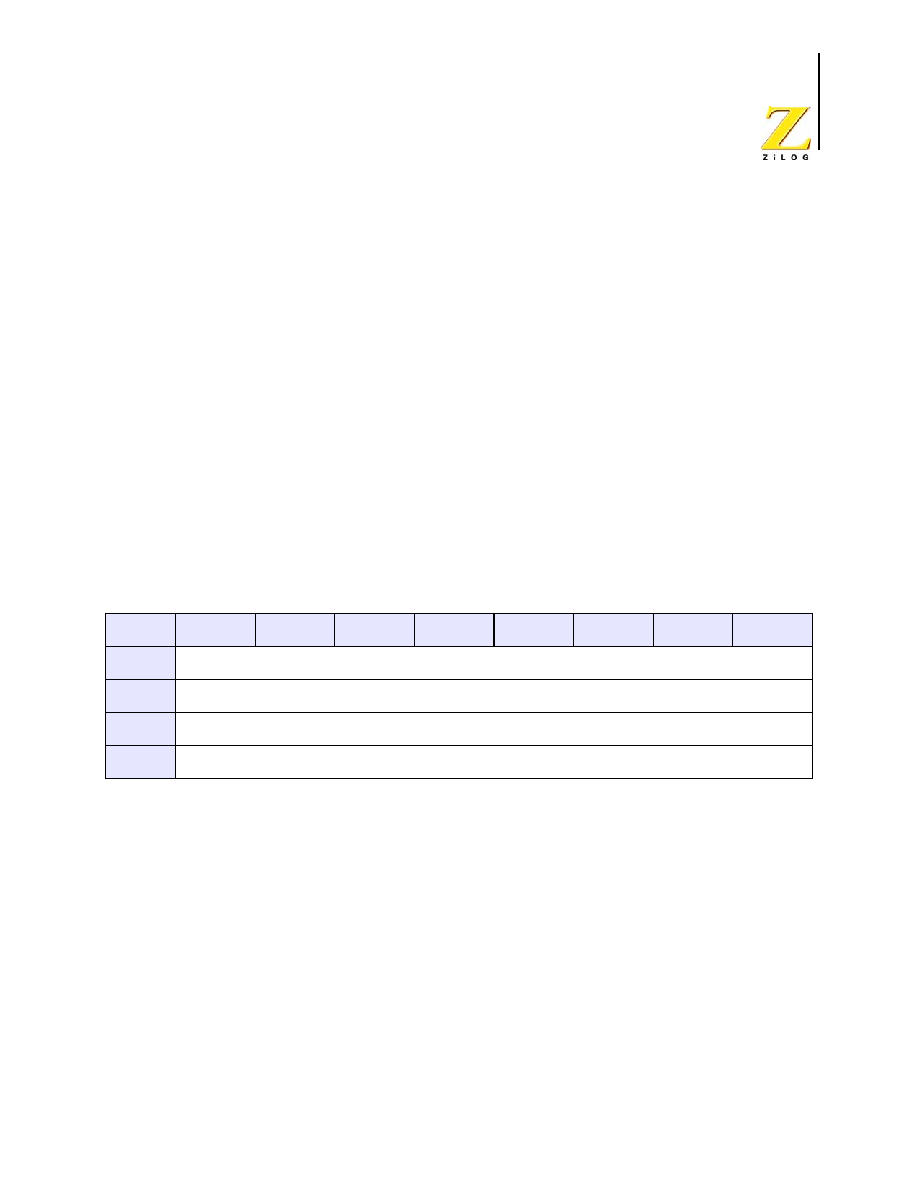
PS019915-1005
Analog-to-Digital
Converter
Z8 Encore!
�
64K Series
Product Specification
176
0100 = ANA4
0101 = ANA5
0110 = ANA6
0111 = ANA7
1000 = ANA8
1001 = ANA9
1010 = ANA10
1011 = ANA11
11XX = Reserved.
ADC Data High Byte Register
The ADC Data High Byte register (Table 86) contains the upper eight bits of the 10-bit
ADC output. During a single-shot conversion, this value is invalid. Access to the ADC
Data High Byte register is read-only. The full 10-bit ADC result is given by
{ADCD_H[7:0], ADCD_L[7:6]}. Reading the ADC Data High Byte register latches data
in the ADC Low Bits register
.
ADCD_H--ADC Data High Byte
This byte contains the upper eight bits of the 10-bit ADC output. These bits are not valid
during a single-shot conversion. During a continuous conversion, the last conversion out-
put is held in this register. These bits are undefined after a Reset.
ADC Data Low Bits Register
The ADC Data Low Bits register (Table 87) contains the lower two bits of the conversion
value. The data in the ADC Data Low Bits register is latched each time the ADC Data
High Byte register is read. Reading this register always returns the lower two bits of the
conversion last read into the ADC High Byte register. Access to the ADC Data Low Bits
Table 86. ADC Data High Byte Register (ADCD_H)
BITS
7
6
5
4
3
2
1
0
FIELD
ADCD_H
RESET
X
R/W
R
ADDR
F72H
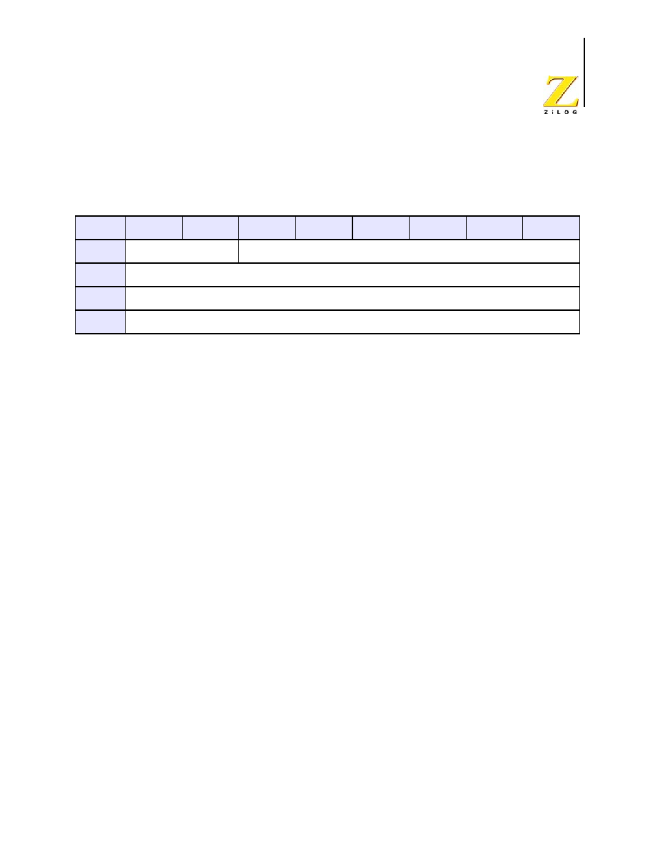
PS019915-1005
Analog-to-Digital
Converter
Z8 Encore!
�
64K Series
Product Specification
177
register is read-only. The full 10-bit ADC result is given by {ADCD_H[7:0],
ADCD_L[7:6]}.
ADCD_L--ADC Data Low Bits
These are the least significant two bits of the 10-bit ADC output. These bits are undefined
after a Reset.
Reserved
These bits are reserved and are always undefined.
Table 87. ADC Data Low Bits Register (ADCD_L)
BITS
7
6
5
4
3
2
1
0
FIELD
ADCD_L
Reserved
RESET
X
R/W
R
ADDR
F73H

Z8 Encore!
�
64K Series
Product Specification
PS019915-1005
Flash
Memory
178
Flash Memory
Overview
The products in the Z8 Encore!
�
64K Series feature up to 64KB (65,536 bytes) of non-
volatile Flash memory with read/write/erase capability. The Flash memory can be pro-
grammed and erased in-circuit by either user code or through the On-Chip Debugger.
The Flash memory array is arranged in 512-byte per page. The 512-byte page is the mini-
mum Flash block size that can be erased. The Flash memory is also divided into 8 sectors
which can be protected from programming and erase operations on a per sector basis.
Table 88 describes the Flash memory configuration for each device in the 64K Series.
Table 89 lists the sector address ranges. Figure 35 illustrates the Flash memory arrange-
ment.
Table 88. Flash Memory Configurations
Part Number
Flash Size
Number of
Pages
Flash Memory
Addresses
Sector Size
Number of
Sectors
Pages per
Sector
Z8F162x
16K (16,384)
32
0000H - 3FFFH
2K (2048)
8
4
Z8F242x
24K (24,576)
48
0000H - 5FFFH
4K (4096)
6
8
Z8F322x
32K (32,768)
64
0000H - 7FFFH
4K (4096)
8
8
Z8F482x
48K (49,152)
96
0000H - BFFFH
8K (8192)
6
16
Z8F642x
64K (65,536)
128
0000H - FFFFH
8K (8192)
8
16
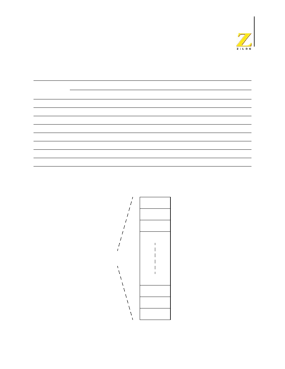
PS019915-1005
Flash
Memory
Z8 Encore!
�
64K Series
Product Specification
179
Figure 35. Flash Memory Arrangement
Table 89. Flash Memory Sector Addresses
Sector Number
Flash Sector Address Ranges
Z8F162x
Z8F242x
Z8F322x
Z8F482x
Z8F642x
0
0000H-07FFH
0000H-0FFFH
0000H-0FFFH
0000H-1FFFH
0000H-1FFFH
1
0800H-0FFFH
1000H-1FFFH
1000H-1FFFH
2000H-3FFFH
2000H-3FFFH
2
1000H-17FFH
2000H-2FFFH
2000H-2FFFH
4000H-5FFFH
4000H-5FFFH
3
1800H-1FFFH
3000H-3FFFH
3000H-3FFFH
6000H-7FFFH
6000H-7FFFH
4
2000H-27FFH
4000H-4FFFH
4000H-4FFFH
8000H-9FFFH
8000H-9FFFH
5
2800H-2FFFH
5000H-5FFFH
5000H-5FFFH
A000H-BFFFH
A000H-BFFFH
6
3000H-37FFH
N/A
6000H-6FFFH
N/A
C000H-DFFFH
7
3800H-3FFFH
N/A
7000H-7FFFH
N/A
E000H-FFFFH
64KB Flash
Program Memory
0000H
128 Pages
512 Bytes per Page
01FFH
0200H
03FFH
FC00H
FDFFH
FE00H
FFFFH
0400H
05FFH
FA00H
FBFFH
Addresses

PS019915-1005
Flash
Memory
Z8 Encore!
�
64K Series
Product Specification
180
Information Area
Table 90 describes the 64K Series Information Area. This 512-byte Information Area is
accessed by setting bit 7 of the Page Select Register to 1. When access is enabled, the
Information Area is mapped into Flash Memory and overlays the 512 bytes at addresses
FE00H
to
FFFFH
. When the Information Area access is enabled, LDC instructions return
data from the Information Area. CPU instruction fetches always comes from Flash Mem-
ory regardless of the Information Area access bit. Access to the Information Area is read-
only.
Operation
The Flash Controller provides the proper signals and timing for Byte Programming, Page
Erase, and Mass Erase of the Flash memory. The Flash Controller contains a protection
mechanism, via the Flash Control register (FCTL), to prevent accidental programming or
erasure. The following subsections provide details on the various operations (Lock,
Unlock, Sector Protect, Byte Programming, Page Erase, and Mass Erase).
Table 90. 64K Series Information Area Map
Flash Memory Address (Hex)
Function
FE00H-FE3FH
Reserved
FE40H-FE53H
Part Number
20-character ASCII alphanumeric code
Left justified and filled with zeros
FE54H-FFFFH
Reserved

PS019915-1005
Flash
Memory
Z8 Encore!
�
64K Series
Product Specification
181
Timing Using the Flash Frequency Registers
Before performing a program or erase operation on the Flash memory, the user must first
configure the Flash Frequency High and Low Byte registers. The Flash Frequency regis-
ters allow programming and erasure of the Flash with system clock frequencies ranging
from 20kHz through 20MHz (the valid range is limited to the device operating frequen-
cies).
The Flash Frequency High and Low Byte registers combine to form a 16-bit value,
FFREQ
, to control timing for Flash program and erase operations. The 16-bit Flash Fre-
quency value must contain the system clock frequency in KHz. This value is calculated
using the following equation:.
Flash programming and erasure are not supported for system clock fre-
quencies below 20KHz, above 20MHz, or outside of the device operating
frequency range. The Flash Frequency High and Low Byte registers must
be loaded with the correct value to insure proper Flash programming and
erase operations.
Flash Read Protection
The user code contained within the Flash memory can be protected from external access.
Programming the Flash Read Protect Option Bit prevents reading of user code by the On-
Chip Debugger or by using the Flash Controller Bypass mode. Refer to the Option Bits
chapter and the On-Chip Debugger chapter for more information.
Flash Write/Erase Protection
The 64K Series provides several levels of protection against accidental program and era-
sure of the Flash memory contents. This protection is provided by the Flash Controller
unlock mechanism, the Flash Sector Protect register, and the Flash Write Protect option
bit.
Flash Controller Unlock Mechanism
At Reset, the Flash Controller locks to prevent accidental program or erasure of the Flash
memory. To program or erase the Flash memory, the Flash controller must be unlocked.
After unlocking the Flash Controller, the Flash can be programmed or erased. Any value
written by user code to the Flash Control register or Page Select Register out of sequence
will lock the Flash Controller.
The proper steps to unlock the Flash Controller from user code are:
1. Write 00H to the Flash Control register to reset the Flash Controller.
FFREQ[15:0]
System Clock Frequency (Hz)
1000
----------------------------------------------------------------------------
=
Caution:

PS019915-1005
Flash
Memory
Z8 Encore!
�
64K Series
Product Specification
182
2. Write the page to be programmed or erased to the Page Select register.
3. Write the first unlock command 73H to the Flash Control register.
4. Write the second unlock command 8CH to the Flash Control register.
5. Re-write the page written in step 2 to the Page Select register.
Flash Sector Protection
The Flash Sector Protect register can be configured to prevent sectors from being pro-
grammed or erased. Once a sector is protected, it cannot be unprotected by user code. The
Flash Sector Protect register is cleared after reset and any previously written protection
values is lost. User code must write this register in their initialization routine if they want
to enable sector protection.
The Flash Sector Protect register shares its Register File address with the Page Select reg-
ister. The Flash Sector Protect register is accessed by writing the Flash Control register
with 5EH. Once the Flash Sector Protect register is selected, it can be accessed at the Page
Select Register address. When user code writes the Flash Sector Protect register, bits can
only be set to 1. Thus, sectors can be protected, but not unprotected, via register write
operations. Writing a value other than 5EH to the Flash Control register de-selects the
Flash Sector Protect register and re-enables access to the Page Select register.
The steps to setup the Flash Sector Protect register from user code are:
1. Write 00H to the Flash Control register to reset the Flash Controller.
2. Write 5EH to the Flash Control register to select the Flash Sector Protect register.
3. Read and/or write the Flash Sector Protect register which is now at Register File
address FF9H.
4. Write 00H to the Flash Control register to return the Flash Controller to its reset state.
Flash Write Protection Option Bit
The Flash Write Protect option bit can be enabled to block all program and erase opera-
tions from user code. Refer to the Option Bits chapter for more information.
Byte Programming
When the Flash Controller is unlocked, writes to Flash Memory from user code will pro-
gram a byte into the Flash if the address is located in the unlocked page. An erased Flash
byte contains all ones (
FFH
). The programming operation can only be used to change bits
from one to zero. To change a Flash bit (or multiple bits) from zero to one requires a Page
Erase or Mass Erase operation.
Byte Programming can be accomplished using the eZ8 CPU's LDC or LDCI instructions.
Refer to the eZ8 CPU User Manual for a description of the LDC and LDCI instructions.

PS019915-1005
Flash
Memory
Z8 Encore!
�
64K Series
Product Specification
183
While the Flash Controller programs the Flash memory, the eZ8 CPU idles but the system
clock and on-chip peripherals continue to operate. Interrupts that occur when a Program-
ming operation is in progress are serviced once the Programming operation is complete.
To exit Programming mode and lock the Flash Controller, write 00H to the Flash Control
register.
User code cannot program Flash Memory on a page that lies in a protected sector. When
user code writes memory locations, only addresses located in the unlocked page are pro-
grammed. Memory writes outside of the unlocked page are ignored.
Each memory location must not be programmed more than twice before an
erase occurs.
The proper steps to program the Flash from user code are:
1. Write 00H to the Flash Control register to reset the Flash Controller.
2. Write the page of memory to be programmed to the Page Select register.
3. Write the first unlock command 73H to the Flash Control register.
4. Write the second unlock command 8CH to the Flash Control register.
5. Re-write the page written in step 2 to the Page Select register.
6. Write Flash Memory using LDC or LDCI instructions to program the Flash.
7. Repeat step 6 to program additional memory locations on the same page.
8. Write 00H to the Flash Control register to lock the Flash Controller.
Page Erase
The Flash memory can be erased one page (512 bytes) at a time. Page Erasing the Flash
memory sets all bytes in that page to the value FFH. The Page Select register identifies the
page to be erased. While the Flash Controller executes the Page Erase operation, the eZ8
CPU idles but the system clock and on-chip peripherals continue to operate. The eZ8 CPU
resumes operation after the Page Erase operation completes. Interrupts that occur when
the Page Erase operation is in progress are serviced once the Page Erase operation is com-
plete. When the Page Erase operation is complete, the Flash Controller returns to its
locked state. Only pages located in unprotected sectors can be erased.
The proper steps to perform a Page Erase operation are:
1. Write 00H to the Flash Control register to reset the Flash Controller.
2. Write the page to be erased to the Page Select register.
3. Write the first unlock command 73H to the Flash Control register.
4. Write the second unlock command 8CH to the Flash Control register.
Caution:

PS019915-1005
Flash
Memory
Z8 Encore!
�
64K Series
Product Specification
184
5. Re-write the page written in step 2 to the Page Select register.
6. Write the Page Erase command 95H to the Flash Control register.
Mass Erase
The Flash memory cannot be Mass Erased by user code.
Flash Controller Bypass
The Flash Controller can be bypassed and the control signals for the Flash memory
brought out to the GPIO pins. Bypassing the Flash Controller allows faster Programming
algorithms by controlling the Flash programming signals directly.
Flash Controller Bypass is recommended for gang programming applications and large
volume customers who do not require in-circuit programming of the Flash memory.
Refer to the document entitled Third-Party Flash Programming Support for Z8 Encore!
�
for more information on bypassing the Flash Controller. This document is available for
download at
www.zilog.com
.
Flash Controller Behavior in Debug Mode
The following changes in behavior of the Flash Controller occur when the Flash Control-
ler is accessed using the On-Chip Debugger:
�
The Flash Write Protect option bit is ignored.
�
The Flash Sector Protect register is ignored for programming and erase operations.
�
Programming operations are not limited to the page selected in the Page Select
register.
�
Bits in the Flash Sector Protect register can be written to one or zero.
�
The second write of the Page Select register to unlock the Flash Controller is not
necessary.
�
The Page Select register can be written when the Flash Controller is unlocked.
�
The Mass Erase command is enabled through the Flash Control register.
For security reasons, flash controller allows only a single page to be
opened for write/erase. When writing multiple flash pages, the flash con-
troller must go through the unlock sequence again to select another page.
Caution:
PS019915-1005
Flash
Memory
Z8 Encore!
�
64K Series
Product Specification
185
Flash Control Register Definitions
Flash Control Register
The Flash Control register (Table 91) unlocks the Flash Controller for programming and
erase operations, or to select the Flash Sector Protect register.
The Write-only Flash Control Register shares its Register File address with the Read-only
Flash Status Register.
FCMD--Flash Command
73H = First unlock command.
8CH = Second unlock command.
95H = Page erase command.
63H = Mass erase command
5EH = Flash Sector Protect register select.
* All other commands, or any command out of sequence, lock the Flash Controller.
Table 91. Flash Control Register (FCTL)
BITS
7
6
5
4
3
2
1
0
FIELD
FCMD
RESET
0
R/W
W
ADDR
FF8H
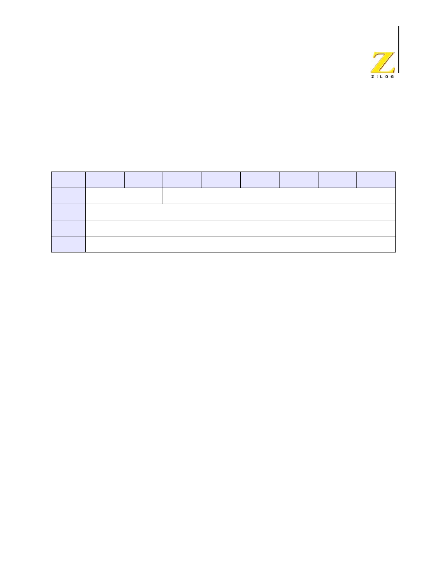
PS019915-1005
Flash
Memory
Z8 Encore!
�
64K Series
Product Specification
186
Flash Status Register
The Flash Status register (Table 92) indicates the current state of the Flash Controller. This
register can be read at any time. The Read-only Flash Status Register shares its Register
File address with the Write-only Flash Control Register.
Reserved
These bits are reserved and must be 0.
FSTAT--Flash Controller Status
00_0000 = Flash Controller locked
00_0001 = First unlock command received
00_0010 = Second unlock command received
00_0011 = Flash Controller unlocked
00_0100 = Flash Sector Protect register selected
00_1xxx = Program operation in progress
01_0xxx = Page erase operation in progress
10_0xxx = Mass erase operation in progress
Table 92. Flash Status Register (FSTAT)
BITS
7
6
5
4
3
2
1
0
FIELD
Reserved
FSTAT
RESET
0
R/W
R
ADDR
FF8H
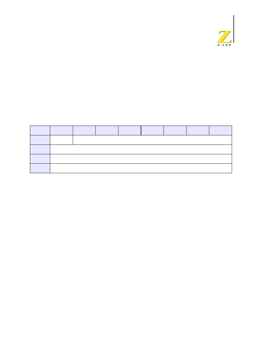
PS019915-1005
Flash
Memory
Z8 Encore!
�
64K Series
Product Specification
187
Page Select Register
The Page Select (FPS) register (Table 93) selects one of the 128 available Flash memory
pages to be erased or programmed. Each Flash Page contains 512 bytes of Flash memory.
During a Page Erase operation, all Flash memory locations with the 7 most significant bits
of the address given by the PAGE field are erased to
FFH
.
The Page Select register shares its Register File address with the Flash Sector Protect Reg-
ister. The Page Select register cannot be accessed when the Flash Sector Protect register is
enabled.
INFO_EN--Information Area Enable
0 = Information Area is not selected.
1 = Information Area is selected. The Information area is mapped into the Flash Memory
address space at addresses FE00H through FFFFH.
PAGE--Page Select
This 7-bit field selects the Flash memory page for Programming and Page Erase opera-
tions. Flash Memory Address[15:9] = PAGE[6:0].
Table 93. Page Select Register (FPS)
BITS
7
6
5
4
3
2
1
0
FIELD
INFO_EN
PAGE
RESET
0
R/W
R/W
ADDR
FF9H

PS019915-1005
Flash
Memory
Z8 Encore!
�
64K Series
Product Specification
188
Flash Sector Protect Register
The Flash Sector Protect register (Table 94) protects Flash memory sectors from being
programmed or erased from user code. The Flash Sector Protect register shares its Regis-
ter File address with the Page Select register. The Flash Sector protect register can be
accessed only after writing the Flash Control register with 5EH.
User code can only write bits in this register to 1 (bits cannot be cleared to 0 by user code).
SECTn--Sector Protect
0 = Sector n can be programmed or erased from user code.
1 = Sector n is protected and cannot be programmed or erased from user code.
* User code can only write bits from 0 to 1.
Table 94. Flash Sector Protect Register (FPROT)
BITS
7
6
5
4
3
2
1
0
FIELD
SECT7
SECT6
SECT5
SECT4
SECT3
SECT2
SECT1
SECT0
RESET
0
R/W
R/W1
ADDR
FF9H
R/W1 = Register is accessible for Read operations. Register can be written to 1 only (via user code).
PS019915-1005
Flash
Memory
Z8 Encore!
�
64K Series
Product Specification
189
Flash Frequency High and Low Byte Registers
The Flash Frequency High and Low Byte registers (Tables 95 and 96) combine to form a
16-bit value, FFREQ, to control timing for Flash program and erase operations. The 16-bit
Flash Frequency registers must be written with the system clock frequency in KHz for
Program and Erase operations. Calculate the Flash Frequency value using the following
equation:
Flash programming and erasure is not supported for system clock frequen-
cies below 20KHz, above 20MHz, or outside of the valid operating fre-
quency range for the device. The Flash Frequency High and Low Byte
registers must be loaded with the correct value to insure proper program
and erase times.
FFREQH and FFREQL--Flash Frequency High and Low Bytes
These 2 bytes, {FFREQH[7:0], FFREQL[7:0]}, contain the 16-bit Flash Frequency value.
Table 95. Flash Frequency High Byte Register (FFREQH)
BITS
7
6
5
4
3
2
1
0
FIELD
FFREQH
RESET
0
R/W
R/W
ADDR
FFAH
Table 96. Flash Frequency Low Byte Register (FFREQL)
BITS
7
6
5
4
3
2
1
0
FIELD
FFREQL
RESET
0
R/W
R/W
ADDR
FFBH
FFREQ[15:0]
FFREQH[7:0],FFREQL[7:0]
{
}
System Clock Frequency
1000
---------------------------------------------------------------
=
=
Caution:

Z8 Encore!
�
64K Series
Product Specification
PS019915-1005
Option
Bits
190
Option Bits
Overview
Option Bits allow user configuration of certain aspects of the 64K Series operation. The
feature configuration data is stored in the Flash Memory and read during Reset. The fea-
tures available for control via the Option Bits are:
�
Watch-Dog Timer time-out response selection�interrupt or Reset.
�
Watch-Dog Timer enabled at Reset.
�
The ability to prevent unwanted read access to user code in Flash Memory.
�
The ability to prevent accidental programming and erasure of the user code in Flash
Memory.
�
Voltage Brown-Out configuration-always enabled or disabled during STOP mode to
reduce STOP mode power consumption.
�
Oscillator mode selection-for high, medium, and low power crystal oscillators, or
external RC oscillator.
Operation
Option Bit Configuration By Reset
Each time the Option Bits are programmed or erased, the device must be Reset for the
change to take place. During any reset operation (System Reset, Reset, or STOP Mode
Recovery), the Option Bits are automatically read from the Flash Memory and written to
Option Configuration registers. The Option Configuration registers control operation of
the devices within the 64K Series. Option Bit control is established before the device exits
Reset and the eZ8 CPU begins code execution. The Option Configuration registers are not
part of the Register File and are not accessible for read or write access.
Option Bit Address Space
The first two bytes of Flash Memory at addresses
0000H
(Table 97) and
0001H
(Table 98)
are reserved for the user Option Bits. The byte at Flash Memory address
0000H
configures
user options. The byte at Flash Memory address
0001H
is reserved for future use and must
remain unprogrammed.

PS019915-1005
Option
Bits
Z8 Encore!
�
64K Series
Product Specification
191
Flash Memory Address 0000H
WDT_RES--Watch-Dog Timer Reset
0 = Watch-Dog Timer time-out generates an interrupt request. Interrupts must be globally
enabled for the eZ8 CPU to acknowledge the interrupt request.
1 = Watch-Dog Timer time-out causes a Short Reset. This setting is the default for unpro-
grammed (erased) Flash.
WDT_AO--Watch-Dog Timer Always On
0 = Watch-Dog Timer is automatically enabled upon application of system power. Watch-
Dog Timer can not be disabled except during STOP Mode (if configured to power down
during STOP Mode).
1 = Watch-Dog Timer is enabled upon execution of the WDT instruction. Once enabled,
the Watch-Dog Timer can only be disabled by a Reset or STOP Mode Recovery. This set-
ting is the default for unprogrammed (erased) Flash.
OSC_SEL[1:0]--Oscillator Mode Selection
00 = On-chip oscillator configured for use with external RC networks (<4MHz).
01 = Minimum power for use with very low frequency crystals (32KHz to 1.0MHz).
10 = Medium power for use with medium frequency crystals or ceramic resonators
(0.5MHz to 10.0MHz).
11 = Maximum power for use with high frequency crystals (8.0MHz to 20.0MHz). This
setting is the default for unprogrammed (erased) Flash.
VBO_AO--Voltage Brown-Out Protection Always On
0 = Voltage Brown-Out Protection is disabled in STOP mode to reduce total power con-
sumption.
1 = Voltage Brown-Out Protection is always enabled including during STOP mode. This
setting is the default for unprogrammed (erased) Flash.
RP--Read Protect
0 = User program code is inaccessible. Limited control features are available through the
On-Chip Debugger.
Table 97. Flash Option Bits At Flash Memory Address 0000H
BITS
7
6
5
4
3
2
1
0
FIELD
WDT_RES WDT_AO
OSC_SEL[1:0]
VBO_AO
RP
Reserved
FWP
RESET
U
R/W
R/W
ADDR
Program Memory 0000H
Note: U = Unchanged by Reset. R/W = Read/Write.
PS019915-1005
Option
Bits
Z8 Encore!
�
64K Series
Product Specification
192
1 = User program code is accessible. All On-Chip Debugger commands are enabled. This
setting is the default for unprogrammed (erased) Flash.
Reserved
These Option Bits are reserved for future use and must always be 1.This setting is the
default for unprogrammed (erased) Flash.
FWP--Flash Write Protect (Flash version only)
Flash Memory Address 0001H
Reserved
These Option Bits are reserved for future use and must always be 1. This setting is the
default for unprogrammed (erased) Flash.
FWP
Description
0
Programming, Page Erase, and Mass Erase through User Code is disabled. Mass Erase
is available through the On-Chip Debugger.
1
Programming, and Page Erase are enabled for all of Flash Program Memory.
Table 98. Options Bits at Flash Memory Address 0001H
BITS
7
6
5
4
3
2
1
0
FIELD
Reserved
RESET
U
R/W
R/W
ADDR
Program Memory 0001H
Note: U = Unchanged by Reset. R = Read-Only. R/W = Read/Write.
Z8 Encore!
�
64K Series
Product Specification
PS019915-1005
On-Chip
Debugger
193
On-Chip Debugger
Overview
The 64K Series products contain an integrated On-Chip Debugger (OCD) that provides
advanced debugging features including:
�
Reading and writing of the Register File
�
Reading and writing of Program and Data Memory
�
Setting of Breakpoints
�
Execution of eZ8 CPU instructions
Architecture
The On-Chip Debugger consists of four primary functional blocks: transmitter, receiver,
auto-baud generator, and debug controller. Figure 36 illustrates the architecture of the On-
Chip Debugger
Figure 36. On-Chip Debugger Block Diagram
Auto-Baud
Detector/Generator
Transmitter
Receiver
Debug Controller
System
Clock
DBG
Pin
eZ8 CPU
Control
PS019915-1005
On-Chip
Debugger
Z8 Encore!
�
64K Series
Product Specification
194
Operation
OCD Interface
The On-Chip Debugger uses the DBG pin for communication with an external host. This
one-pin interface is a bi-directional open-drain interface that transmits and receives data.
Data transmission is half-duplex, in that transmit and receive cannot occur simultaneously.
The serial data on the DBG pin is sent using the standard asynchronous data format
defined in RS-232. This pin can interface the 64K Series products to the serial port of a
host PC using minimal external hardware.Two different methods for connecting the DBG
pin to an RS-232 interface are depicted in Figures 37 and 38.
For operation of the On-Chip Debugger, all power pins (V
DD
and AV
DD
)
must be supplied with power, and all ground pins (V
SS
and AV
SS
) must be
properly grounded.
The DBG pin is open-drain and must always be connected to V
DD
through
an external pull-up resistor to ensure proper operation.
Figure 37. Interfacing the On-Chip Debugger's DBG Pin with an RS-232 Interface (1)
Caution:
RS-232 TX
RS-232 RX
RS-232
Transceiver
V
DD
DBG Pin
10K Ohm
Diode
PS019915-1005
On-Chip
Debugger
Z8 Encore!
�
64K Series
Product Specification
195
Figure 38. Interfacing the On-Chip Debugger's DBG Pin with an RS-232 Interface (2)
Debug Mode
The operating characteristics of the 64K Series devices in DEBUG mode are:
�
The eZ8 CPU fetch unit stops, idling the eZ8 CPU, unless directed by the OCD to
execute specific instructions.
�
The system clock operates unless in STOP mode.
�
All enabled on-chip peripherals operate unless in STOP mode.
�
Automatically exits HALT mode.
�
Constantly refreshes the Watch-Dog Timer, if enabled.
Entering Debug Mode
The device enters DEBUG mode following any of the following operations:
�
Writing the DBGMODE bit in the OCD Control Register to 1 using the OCD interface.
�
eZ8 CPU execution of a BRK (Breakpoint) instruction (when enabled).
�
If the DBG pin is Low when the device exits Reset, the On-Chip Debugger
automatically puts the device into DEBUG mode.
Exiting Debug Mode
The device exits DEBUG mode following any of the following operations:
�
Clearing the DBGMODE bit in the OCD Control Register to 0.
�
Power-on reset
�
Voltage Brown Out reset
RS-232 TX
RS-232 RX
RS-232
Transceiver
V
DD
DBG Pin
10K Ohm
Open-Drain
Buffer

PS019915-1005
On-Chip
Debugger
Z8 Encore!
�
64K Series
Product Specification
196
�
Asserting the RESET pin Low to initiate a Reset.
�
Driving the DBG pin Low while the device is in STOP mode initiates a System Reset.
OCD Data Format
The OCD interface uses the asynchronous data format defined for RS-232. Each character
is transmitted as 1 Start bit, 8 data bits (least-significant bit first), and 1 Stop bit
(Figure 39).
Figure 39. OCD Data Format
OCD Auto-Baud Detector/Generator
To run over a range of baud rates (bits per second) with various system clock frequencies,
the On-Chip Debugger has an Auto-Baud Detector/Generator. After a reset, the OCD is
idle until it receives data. The OCD requires that the first character sent from the host is
the character
80H
. The character
80H
has eight continuous bits Low (one Start bit plus 7
data bits). The Auto-Baud Detector measures this period and sets the OCD Baud Rate
Generator accordingly.
The Auto-Baud Detector/Generator is clocked by the system clock. The minimum baud
rate is the system clock frequency divided by 512. For optimal operation, the maximum
recommended baud rate is the system clock frequency divided by 8. The theoretical maxi-
mum baud rate is the system clock frequency divided by 4. This theoretical maximum is
possible for low noise designs with clean signals. Table 99 lists minimum and recom-
mended maximum baud rates for sample crystal frequencies.
If the OCD receives a Serial Break (nine or more continuous bits Low) the Auto-Baud
Detector/Generator resets. The Auto-Baud Detector/Generator can then be reconfigured
by sending
80H
.
Table 99. OCD Baud-Rate Limits
System Clock Frequency
(MHz)
Recommended Maximum Baud Rate
(kbits/s)
Minimum Baud Rate
(kbits/s)
20.0
2500
39.1
1.0
125.0
1.96
0.032768 (32KHz)
4.096
0.064
START
D0
D1
D2
D3
D4
D5
D6
D7
STOP

PS019915-1005
On-Chip
Debugger
Z8 Encore!
�
64K Series
Product Specification
197
OCD Serial Errors
The On-Chip Debugger can detect any of the following error conditions on the DBG pin:
�
Serial Break (a minimum of nine continuous bits Low)
�
Framing Error (received Stop bit is Low)
�
Transmit Collision (OCD and host simultaneous transmission detected by the OCD)
When the OCD detects one of these errors, it aborts any command currently in progress,
transmits a Serial Break 4096 system clock cycles long back to the host, and resets the
Auto-Baud Detector/Generator. A Framing Error or Transmit Collision may be caused by
the host sending a Serial Break to the OCD. Because of the open-drain nature of the inter-
face, returning a Serial Break break back to the host only extends the length of the Serial
Break if the host releases the Serial Break early.
The host transmits a Serial Break on the DBG pin when first connecting to the 64K Series
devices or when recovering from an error. A Serial Break from the host resets the Auto-
Baud Generator/Detector but does not reset the OCD Control register. A Serial Break
leaves the device in DEBUG mode if that is the current mode. The OCD is held in Reset
until the end of the Serial Break when the DBG pin returns High. Because of the open-
drain nature of the DBG pin, the host can send a Serial Break to the OCD even if the OCD
is transmitting a character.
Breakpoints
Execution Breakpoints are generated using the BRK instruction (opcode 00H). When the
eZ8 CPU decodes a BRK instruction, it signals the On-Chip Debugger. If Breakpoints are
enabled, the OCD idles the eZ8 CPU and enters DEBUG mode. If Breakpoints are not
enabled, the OCD ignores the BRK signal and the BRK instruction operates as an NOP.
If breakpoints are enabled, the OCD can be configured to automatically enter DEBUG
mode, or to loop on the break instruction. If the OCD is configured to loop on the BRK
instruction, then the CPU is still enabled to service DMA and interrupt requests.
The loop on BRK instruction can be used to service interrupts in the background. For
interrupts to be serviced in the background, there cannot be any breakpoints in the inter-
rupt service routine. Otherwise, the CPU stops on the breakpoint in the interrupt routine.
For interrupts to be serviced in the background, interrupts must also be enabled. Debug-
ging software should not automatically enable interrupts when using this feature, since
interrupts are typically disabled during critical sections of code where interrupts should
not occur (such as adjusting the stack pointer or modifying shared data).
Software can poll the IDLE bit of the OCDSTAT register to determine if the OCD is loop-
ing on a BRK instruction. When software wants to stop the CPU on the BRK instruction it
is looping on, software should not set the DBGMODE bit of the OCDCTL register. The
CPU may have vectored to and be in the middle of an interrupt service routine when this
bit gets set. Instead, software must clear the BRKLP bit. This action allows the CPU to

PS019915-1005
On-Chip
Debugger
Z8 Encore!
�
64K Series
Product Specification
198
finish the interrupt service routine it may be in and return the BRK instruction. When the
CPU returns to the BRK instruction it was previously looping on, it automatically sets the
DBGMODE bit and enter DEBUG mode.
Software detects that the majority of the OCD commands are still disabled when the eZ8
CPU is looping on a BRK instruction. The eZ8 CPU must be stopped and the part must be
in DEBUG mode before these commands can be issued.
Breakpoints in Flash Memory
The BRK instruction is opcode
00H
, which corresponds to the fully programmed state of a
byte in Flash memory. To implement a Breakpoint, write
00H
to the desired address, over-
writing the current instruction. To remove a Breakpoint, the corresponding page of Flash
memory must be erased and reprogrammed with the original data.
On-Chip Debugger Commands
The host communicates to the On-Chip Debugger by sending OCD commands using the
DBG interface. During normal operation, only a subset of the OCD commands are avail-
able. In DEBUG mode, all OCD commands become available unless the user code and
control registers are protected by programming the Read Protect Option Bit (RP). The
Read Protect Option Bit prevents the code in memory from being read out of the 64K
Series products. When this option is enabled, several of the OCD commands are disabled.
Table 100 contains a summary of the On-Chip Debugger commands. Each OCD com-
mand is described in further detail in the bulleted list following Table 100. Table 100 indi-
cates those commands that operate when the device is not in DEBUG mode (normal
operation) and those commands that are disabled by programming the Read Protect
Option Bit.
Table 100. On-Chip Debugger Commands
Debug Command
Command Byte
Enabled when NOT
in DEBUG mode?
Disabled by
Read Protect Option Bit
Read OCD Revision
00H
Yes
-
Read OCD Status Register
02H
Yes
-
Read Runtime Counter
03H
-
-
Write OCD Control Register
04H
Yes
Cannot clear DBGMODE bit
Read OCD Control Register
05H
Yes
-
Write Program Counter
06H
-
Disabled
Read Program Counter
07H
-
Disabled

PS019915-1005
On-Chip
Debugger
Z8 Encore!
�
64K Series
Product Specification
199
In the following bulleted list of OCD Commands, data and commands sent from the host
to the On-Chip Debugger are identified by '
DBG
Command/Data
'. Data sent from the
On-Chip Debugger back to the host is identified by '
DBG
Data
'
�
Read OCD Revision (00H)--The Read OCD Revision command determines the
version of the On-Chip Debugger. If OCD commands are added, removed, or
changed, this revision number changes.
DBG
00H
DBG
OCDREV[15:8] (Major revision number)
DBG
OCDREV[7:0] (Minor revision number)
�
Read OCD Status Register (02H)--The Read OCD Status Register command reads
the OCDSTAT register.
DBG
02H
DBG
OCDSTAT[7:0]
�
Write OCD Control Register (04H)--The Write OCD Control Register command
writes the data that follows to the OCDCTL register. When the Read Protect Option
Bit is enabled, the DBGMODE bit (OCDCTL[7]) can only be set to 1, it cannot be
cleared to 0 and the only method of putting the device back into normal operating
mode is to reset the device.
Write Register
08H
-
Only writes of the Flash Memory Control
registers are allowed. Additionally, only the
Mass Erase command is allowed to be
written to the Flash Control register.
Read Register
09H
-
Disabled-
Write Program Memory
0AH
-
Disabled
Read Program Memory
0BH
-
Disabled
Write Data Memory
0CH
-
Disabled
Read Data Memory
0DH
-
Disabled
Read Program Memory CRC
0EH
-
-
Reserved
0FH
-
-
Step Instruction
10H
-
Disabled
Stuff Instruction
11H
-
Disabled
Execute Instruction
12H
-
Disabled
Reserved
13H - FFH
-
-
Table 100. On-Chip Debugger Commands (Continued)
Debug Command
Command Byte
Enabled when NOT
in DEBUG mode?
Disabled by
Read Protect Option Bit

PS019915-1005
On-Chip
Debugger
Z8 Encore!
�
64K Series
Product Specification
200
DBG
04H
DBG
OCDCTL[7:0]
�
Read OCD Control Register (05H)--The Read OCD Control Register command
reads the value of the OCDCTL register.
DBG
05H
DBG
OCDCTL[7:0]
�
Write Program Counter (06H)--The Write Program Counter command writes the
data that follows to the eZ8 CPU's Program Counter (PC). If the device is not in
DEBUG mode or if the Read Protect Option Bit is enabled, the Program Counter (PC)
values are discarded.
DBG
06H
DBG
ProgramCounter[15:8]
DBG
ProgramCounter[7:0]
�
Read Program Counter (07H)--The Read Program Counter command reads the
value in the eZ8 CPU's Program Counter (PC). If the device is not in DEBUG mode
or if the Read Protect Option Bit is enabled, this command returns
FFFFH
.
DBG
07H
DBG
ProgramCounter[15:8]
DBG
ProgramCounter[7:0]
�
Write Register (08H)--The Write Register command writes data to the Register File.
Data can be written 1-256 bytes at a time (256 bytes can be written by setting size to
zero). If the device is not in DEBUG mode, the address and data values are discarded.
If the Read Protect Option Bit is enabled, then only writes to the Flash Control
Registers are allowed and all other register write data values are discarded.
DBG
08H
DBG
{4'h0,Register Address[11:8]}
DBG
Register Address[7:0]
DBG
Size[7:0]
DBG
1-256 data bytes
�
Read Register (09H)--The Read Register command reads data from the Register
File. Data can be read 1-256 bytes at a time (256 bytes can be read by setting size to
zero). If the device is not in DEBUG mode or if the Read Protect Option Bit is
enabled, this command returns
FFH
for all the data values.
DBG
09H
DBG
{4'h0,Register Address[11:8]
DBG
Register Address[7:0]
DBG
Size[7:0]
DBG
1-256 data bytes
�
Write Program Memory (0AH)--The Write Program Memory command writes data
to Program Memory. This command is equivalent to the LDC and LDCI instructions.
Data can be written 1-65536 bytes at a time (65536 bytes can be written by setting size
to zero). The on-chip Flash Controller must be written to and unlocked for the

PS019915-1005
On-Chip
Debugger
Z8 Encore!
�
64K Series
Product Specification
201
programming operation to occur. If the Flash Controller is not unlocked, the data is
discarded. If the device is not in DEBUG mode or if the Read Protect Option Bit is
enabled, the data is discarded.
DBG
0AH
DBG
Program Memory Address[15:8]
DBG
Program Memory Address[7:0]
DBG
Size[15:8]
DBG
Size[7:0]
DBG
1-65536 data bytes
�
Read Program Memory (0BH)--The Read Program Memory command reads data
from Program Memory. This command is equivalent to the LDC and LDCI
instructions. Data can be read 1-65536 bytes at a time (65536 bytes can be read by
setting size to zero). If the device is not in DEBUG mode or if the Read Protect Option
Bit is enabled, this command returns
FFH
for the data.
DBG
0BH
DBG
Program Memory Address[15:8]
DBG
Program Memory Address[7:0]
DBG
Size[15:8]
DBG
Size[7:0]
DBG
1-65536 data bytes
�
Write Data Memory (0CH)--The Write Data Memory command writes data to Data
Memory. This command is equivalent to the LDE and LDEI instructions. Data can be
written 1-65536 bytes at a time (65536 bytes can be written by setting size to zero). If
the device is not in DEBUG mode or if the Read Protect Option Bit is enabled, the
data is discarded.
DBG
0CH
DBG
Data Memory Address[15:8]
DBG
Data Memory Address[7:0]
DBG
Size[15:8]
DBG
Size[7:0]
DBG
1-65536 data bytes
�
Read Data Memory (0DH)--The Read Data Memory command reads from Data
Memory. This command is equivalent to the LDE and LDEI instructions. Data can be
read 1-65536 bytes at a time (65536 bytes can be read by setting size to zero). If the
device is not in DEBUG mode, this command returns
FFH
for the data.
DBG
0DH
DBG
Data Memory Address[15:8]
DBG
Data Memory Address[7:0]
DBG
Size[15:8]
DBG
Size[7:0]
DBG
1-65536 data bytes
�
Read Program Memory CRC (0EH)--The Read Program Memory CRC command
computes and returns the CRC (cyclic redundancy check) of Program Memory using

PS019915-1005
On-Chip
Debugger
Z8 Encore!
�
64K Series
Product Specification
202
the 16-bit CRC-CCITT polynomial. If the device is not in DEBUG mode, this
command returns
FFFFH
for the CRC value. Unlike most other OCD Read
commands, there is a delay from issuing of the command until the OCD returns the
data. The OCD reads the Program Memory, calculates the CRC value, and returns the
result. The delay is a function of the Program Memory size and is approximately equal
to the system clock period multiplied by the number of bytes in the Program Memory.
DBG
0EH
DBG
CRC[15:8]
DBG
CRC[7:0]
�
Step Instruction (10H)--The Step Instruction command steps one assembly
instruction at the current Program Counter (PC) location. If the device is not in
DEBUG mode or the Read Protect Option Bit is enabled, the OCD ignores this
command.
DBG
10H
�
Stuff Instruction (11H)--The Stuff Instruction command steps one assembly
instruction and allows specification of the first byte of the instruction. The remaining
0-4 bytes of the instruction are read from Program Memory. This command is useful
for stepping over instructions where the first byte of the instruction has been
overwritten by a Breakpoint. If the device is not in DEBUG mode or the Read Protect
Option Bit is enabled, the OCD ignores this command.
DBG
11H
DBG
opcode[7:0]
�
Execute Instruction (12H)--The Execute Instruction command allows sending an
entire instruction to be executed to the eZ8 CPU. This command can also step over
Breakpoints. The number of bytes to send for the instruction depends on the opcode. If
the device is not in DEBUG mode or the Read Protect Option Bit is enabled, the OCD
ignores this command
DBG
12H
DBG
1-5 byte opcode
On-Chip Debugger Control Register Definitions
OCD Control Register
The OCD Control register (Table 101) controls the state of the On-Chip Debugger. This
register enters or exits DEBUG mode and enables the BRK instruction. It can also reset
the Z8F642x familyZ8R642x family device.
PS019915-1005
On-Chip
Debugger
Z8 Encore!
�
64K Series
Product Specification
203
A "reset and stop" function can be achieved by writing
81H
to this register. A "reset and
go" function can be achieved by writing
41H
to this register. If the device is in DEBUG
mode, a "run" function can be implemented by writing
40H
to this register.
DBGMODE--Debug Mode
Setting this bit to 1 causes the device to enter DEBUG mode. When in DEBUG mode, the
eZ8 CPU stops fetching new instructions. Clearing this bit causes the eZ8 CPU to start
running again. This bit is automatically set when a BRK instruction is decoded and Break-
points are enabled. If the Read Protect Option Bit is enabled, this bit can only be cleared
by resetting the device, it cannot be written to 0.
0 = The 64K Series device is operating in Normal mode.
1 = The 64K Series device is in DEBUG mode.
BRKEN--Breakpoint Enable
This bit controls the behavior of the BRK instruction (opcode 00H). By default, Break-
points are disabled and the BRK instruction behaves like a NOP. If this bit is set to 1 and a
BRK instruction is decoded, the OCD takes action dependent upon the BRKLOOP bit.
0 = BRK instruction is disabled.
1 = BRK instruction is enabled.
DBGACK--Debug Acknowledge
This bit enables the debug acknowledge feature. If this bit is set to 1, then the OCD sends
an Debug Acknowledge character (
FFH
) to the host when a Breakpoint occurs.
0 = Debug Acknowledge is disabled.
1 = Debug Acknowledge is enabled.
BRKLOOP--Breakpoint Loop
This bit determines what action the OCD takes when a BRK instruction is decoded if
breakpoints are enabled (BRKEN is 1). If this bit is 0, then the DBGMODE bit is automat-
ically set to 1 and the OCD entered DEBUG mode. If BRKLOOP is set to 1, then the eZ8
CPU loops on the BRK instruction.
0 = BRK instruction sets DBGMODE to 1.
1 = eZ8 CPU loops on BRK instruction.
Reserved
These bits are reserved and must be 0.
Table 101. OCD Control Register (OCDCTL)
BITS
7
6
5
4
3
2
1
0
FIELD
DBGMODE
BRKEN DBGACK BRKLOOP
Reserved
RST
RESET
0
R/W
R/W
R
R/W
PS019915-1005
On-Chip
Debugger
Z8 Encore!
�
64K Series
Product Specification
204
RST--Reset
Setting this bit to 1 resets the 64K Series devices. The devices go through a normal Power-
On Reset sequence with the exception that the On-Chip Debugger is not reset. This bit is
automatically cleared to 0 when the reset finishes.
0 = No effect
1 = Reset the 64K Series device
OCD Status Register
The OCD Status register (Table 102) reports status information about the current state of
the debugger and the system.
IDLE--CPU idling
This bit is set if the part is in DEBUG mode (DBGMODE is 1), or if a BRK instruction
occurred since the last time OCDCTL was written. This can be used to determine if the
CPU is running or if it is idling.
0 = The eZ8 CPU is running.
1 = The eZ8 CPU is either stopped or looping on a BRK instruction.
HALT--HALT Mode
0 = The device is not in HALT mode.
1 = The device is in HALT mode.
RPEN--Read Protect Option Bit Enabled
0 = The Read Protect Option Bit is disabled (1).
1 = The Read Protect Option Bit is enabled (0), disabling many OCD commands.
Reserved
These bits are always 0.
Table 102. OCD Status Register (OCDSTAT)
BITS
7
6
5
4
3
2
1
0
FIELD
IDLE
HALT
RPEN
Reserved
RESET
0
R/W
R

Z8 Encore!
�
64K Series
Product Specification
PS019915-1005
On-Chip
Oscillator
205
On-Chip Oscillator
Overview
The products in the 64K Series feature an on-chip oscillator for use with external crystals
with frequencies from 32KHz to 20MHz. In addition, the oscillator can support external
RC networks with oscillation frequencies up to 4MHz or ceramic resonators with oscilla-
tion frequencies up to 20MHz. This oscillator generates the primary system clock for the
internal eZ8 CPU and the majority of the on-chip peripherals. Alternatively, the X
IN
input
pin can also accept a CMOS-level clock input signal (32KHz�20MHz). If an external
clock generator is used, the X
OUT
pin must be left unconnected.
When configured for use with crystal oscillators or external clock drivers, the frequency of
the signal on the X
IN
input pin determines the frequency of the system clock (that is, no
internal clock divider). In RC operation, the system clock is driven by a clock divider
(divide by 2) to ensure 50% duty cycle.
Operating Modes
The 64K Series products support 4 different oscillator modes:
�
On-chip oscillator configured for use with external RC networks (<4MHz).
�
Minimum power for use with very low frequency crystals (32KHz to 1.0MHz).
�
Medium power for use with medium frequency crystals or ceramic resonators
(0.5MHz to 10.0MHz).
�
Maximum power for use with high frequency crystals or ceramic resonators (8.0MHz
to 20.0MHz).
The oscillator mode is selected through user-programmable Option Bits. Refer to the
Option Bits chapter for information.
Crystal Oscillator Operation
Figure 40 illustrates a recommended configuration for connection with an external funda-
mental-mode, parallel-resonant crystal operating at 20MHz. Recommended 20MHz crys-
tal specifications are provided in Table 103. Resistor R1 is optional and limits total power
dissipation by the crystal. The printed circuit board layout must add no more than 4pF of
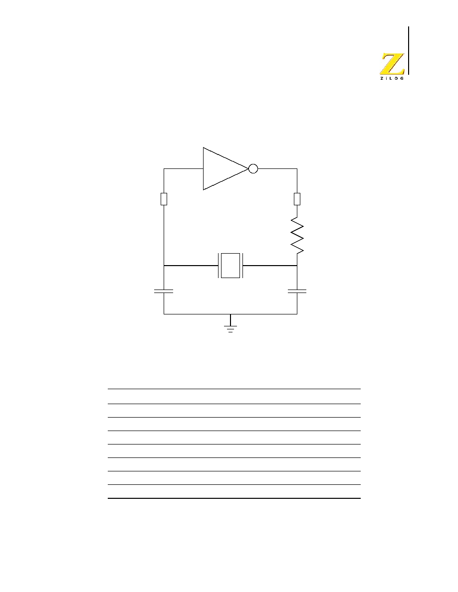
PS019915-1005
On-Chip
Oscillator
Z8 Encore!
�
64K Series
Product Specification
206
stray capacitance to either the X
IN
or X
OUT
pins. If oscillation does not occur, reduce the
values of capacitors C1 and C2 to decrease loading.
Figure 40. Recommended 20MHz Crystal Oscillator Configuration
Table 103. Recommended Crystal Oscillator Specifications (20MHz Operation)
Parameter
Value
Units
Comments
Frequency
20
MHz
Resonance
Parallel
Mode
Fundamental
Series Resistance (R
S
)
25
Maximum
Load Capacitance (C
L
)
20
pF
Maximum
Shunt Capacitance (C
0
)
7
pF
Maximum
Drive Level
1
mW
Maximum
C2 = 22pF
C1 = 22pF
Crystal
XOUT
XIN
On-Chip Oscillator
R1 = 220
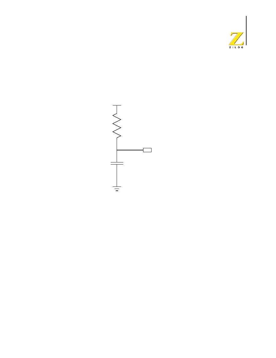
PS019915-1005
On-Chip
Oscillator
Z8 Encore!
�
64K Series
Product Specification
207
Oscillator Operation with an External RC Network
The External RC oscillator mode is applicable to timing insensitive applications.
Figure 41 illustrates a recommended configuration for connection with an external resis-
tor-capacitor (RC) network.
Figure 41. Connecting the On-Chip Oscillator to an External RC Network
An external resistance value of 45k
is recommended for oscillator operation with an
external RC network. The minimum resistance value to ensure operation is 40k
. The
typical oscillator frequency can be estimated from the values of the resistor (R in k
) and
capacitor (C in pF) elements using the following equation:
Figure 42 illustrates the typical (3.3V and 25
0
C) oscillator frequency as a function of the
capacitor (C in pF) employed in the RC network assuming a 45k
external resistor. For
very small values of C, the parasitic capacitance of the oscillator XIN pin and the printed
circuit board should be included in the estimation of the oscillator frequency.
It is possible to operate the RC oscillator using only the parasitic capacitance of the pack-
age and printed circuit board. To minimize sensitivity to external parasitics, external
capacitance values in excess of 20pF are recommended.
C
X
IN
R
V
DD
Oscillator Frequency (kHz)
1
6
�10
0.4 R C
�
�
(
)
4 C
�
(
)
+
---------------------------------------------------------
=
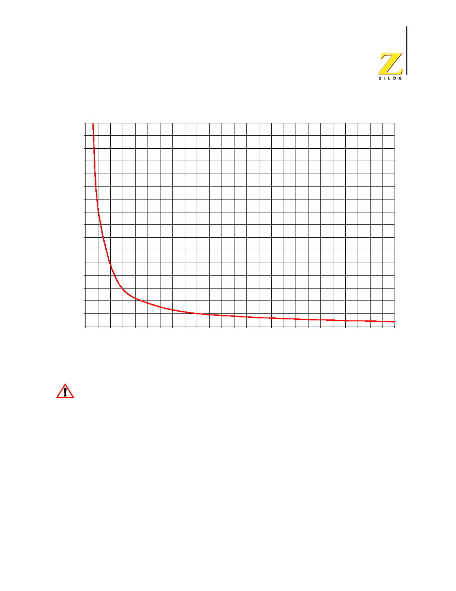
PS019915-1005
On-Chip
Oscillator
Z8 Encore!
�
64K Series
Product Specification
208
Figure 42. Typical RC Oscillator Frequency as a Function of the External Capacitance with a 45k
Resistor
When using the external RC oscillator mode, the oscillator may stop oscil-
lating if the power supply drops below 2.7V, but before the power supply
drops to the voltage brown-out threshold. The oscillator will resume oscil-
lation as soon as the supply voltage exceeds 2.7V.
0
250
500
750
1000
1250
1500
1750
2000
2250
2500
2750
3000
3250
3500
3750
4000
0
20
40
60
80 100 120 140 160 180 200 220 240 260 280 300 320 340 360 380 400 420 440 460 480 500
C (pF)
F
r
e
q
uency
(kHz
)
Caution:

Z8 Encore!
�
64K Series
Product Specification
PS019915-1005
Electrical
Characteristics
209
Electrical Characteristics
Absolute Maximum Ratings
Stresses greater than those listed in Table 104 may cause permanent damage to the device.
These ratings are stress ratings only. Operation of the device at any condition outside those
indicated in the operational sections of these specifications is not implied. Exposure to
absolute maximum rating conditions for extended periods may affect device reliability.
For improved reliability, unused inputs must be tied to one of the supply voltages (V
DD
or
V
SS
).
Table 104. Absolute Maximum Ratings
Parameter
Minimum Maximum
Units
Notes
Ambient temperature under bias
-40
+125
C
Storage temperature
�65
+150
C
Voltage on any pin with respect to V
SS
�0.3
+5.5
V
1
Voltage on V
DD
pin with respect to V
SS
�0.3
+3.6
V
Maximum current on input and/or inactive output pin
�5
+5
�A
Maximum output current from active output pin
-25
+25
mA
80-Pin QFP Maximum Ratings at �40�C to 70�C
Total power dissipation
550
mW
Maximum current into V
DD
or out of V
SS
150
mA
80-Pin QFP Maximum Ratings at 70�C to 125�C
Total power dissipation
200
mW
Maximum current into V
DD
or out of V
SS
56
mA
68-Pin PLCC Maximum Ratings at �40�C to 70�C
Total power dissipation
1000
mW
Maximum current into V
DD
or out of V
SS
275
mA
68-Pin PLCC Maximum Ratings at 70
0
C to 125
0
C
Notes:
1. This voltage applies to all pins except the following: VDD, AVDD, pins supporting analog input (Ports B and H),
RESET, and where noted otherwise.

PS019915-1005
Electrical
Characteristics
Z8 Encore!
�
64K Series
Product Specification
210
Total power dissipation
500
mW
Maximum current into V
DD
or out of V
SS
140
mA
64-Pin LQFP Maximum Ratings at �40�C to 70�C
Total power dissipation
1000
mW
Maximum current into V
DD
or out of V
SS
275
mA
64-Pin LQFP Maximum Ratings at 70
0
C to 125
0
C
Total power dissipation
540
mW
Maximum current into V
DD
or out of V
SS
150
mA
44-Pin PLCC Maximum Ratings at �40�C to 70�C
Total power dissipation
750
mW
Maximum current into V
DD
or out of V
SS
200
mA
44-Pin PLCC Maximum Ratings at 70
0
C to 125
0
C
Total power dissipation
295
mW
Maximum current into V
DD
or out of V
SS
83
mA
44-pin LQFP Maximum Ratings at �40�C to 70�C
Total power dissipation
750
mW
Maximum current into V
DD
or out of V
SS
200
mA
44-pin LQFP Maximum Ratings at 70
0
C to 125
0
C
Total power dissipation
360
mW
Maximum current into V
DD
or out of V
SS
100
mA
40-pin PDIP Maximum Ratings at �40�C to 70�C
Total power dissipation
1000
mW
Maximum current into V
DD
or out of V
SS
275
mA
40-pin PDIP Maximum Ratings at 70
0
C to 125
0
C
Total power dissipation
540
mW
Maximum current into V
DD
or out of V
SS
150
mA
Table 104. Absolute Maximum Ratings (Continued)
Parameter
Minimum Maximum
Units
Notes
Notes:
1. This voltage applies to all pins except the following: VDD, AVDD, pins supporting analog input (Ports B and H),
RESET, and where noted otherwise.
PS019915-1005
Electrical
Characteristics
Z8 Encore!
�
64K Series
Product Specification
211
DC Characteristics
Table 105 lists the DC characteristics of the 64K Series products. All voltages are refer-
enced to V
SS
, the primary system ground.
Table 105. DC Characteristics
Symbol Parameter
T
A
= �40
0
C to 125
0
C
Units Conditions
Minimum Typical Maximum
V
DD
Supply Voltage
3.0
�
3.6
V
V
IL1
Low Level Input Voltage
-0.3
�
0.3*V
DD
V
For all input pins except RESET,
DBG, XIN
V
IL2
Low Level Input Voltage
-0.3
�
0.2*V
DD
V
For RESET, DBG, and XIN.
V
IH1
High Level Input Voltage
0.7*V
DD
�
5.5
V
Port A, C, D, E, F, and G pins.
V
IH2
High Level Input Voltage
0.7*V
DD
�
V
DD
+0.3
V
Port B and H pins.
V
IH3
High Level Input Voltage
0.8*V
DD
�
V
DD
+0.3
V
RESET, DBG, and XIN pins
V
OL1
Low Level Output Voltage
Standard Drive
�
�
0.4
V
I
OL
= 2mA; VDD = 3.0V
High Output Drive disabled.
V
OH1
High Level Output Voltage
Standard Drive
2.4
�
�
V
I
OH
= -2mA; VDD = 3.0V
High Output Drive disabled.
V
OL2
Low Level Output Voltage
High Drive
�
�
0.6
V
I
OL
= 20mA; VDD = 3.3V
High Output Drive enabled
T
A
= -40
0
C to +70
0
C
V
OH2
High Level Output Voltage
High Drive
2.4
�
�
V
I
OH
= -20mA; VDD = 3.3V
High Output Drive enabled;
T
A
= -40
0
C to +70
0
C
V
OL3
Low Level Output Voltage
High Drive
�
�
0.6
V
I
OL
= 15mA; VDD = 3.3V
High Output Drive enabled;
T
A
= +70
0
C to +105
0
C
V
OH3
High Level Output Voltage
High Drive
2.4
�
�
V
I
OH
= 15mA; VDD = 3.3V
High Output Drive enabled;
T
A
= +70
0
C to +105
0
C
V
RAM
RAM Data Retention
0.7
�
�
V
I
IL
Input Leakage Current
-5
�
+5
A V
DD
= 3.6V;
V
IN
= VDD or VSS
1
I
TL
Tri-State Leakage Current
-5
�
+5
A V
DD
= 3.6V
C
PAD
GPIO Port Pad Capacitance
�
8.0
2
�
pF
C
XIN
XIN Pad Capacitance
�
8.0
2
�
pF
PS019915-1005
Electrical
Characteristics
Z8 Encore!
�
64K Series
Product Specification
212
C
XOUT
XOUT Pad Capacitance
�
9.5
2
�
pF
I
PU
Weak Pull-up Current
30
100
350
A V
DD
= 3.0 - 3.6 V
I
DDA
Active Mode Supply Current
(See Figures 43 and 44)
GPIO pins configured as
outputs
�
11
16
12
mA V
DD
= 3.6 V, Fsysclk = 20 MHz
V
DD
= 3.3 V
�
9
11
9
mA V
DD
= 3.6 V, Fsysclk = 10 MHz
V
DD
= 3.3 V
I
DDH
Halt Mode Supply Current
(See Figures 45 and 46)
GPIO pins configured as
outputs
4
7
5
mA V
DD
= 3.6 V, Fsysclk = 20 MHz
V
DD
= 3.3 V
�
3
5
4
mA V
DD
= 3.6 V, Fsysclk = 10 MHz
V
DD
= 3.3 V
I
DDS
Stop Mode Supply Current
(See Figures 47 and 48)
GPIO pins configured as
outputs
�
520
700
650
A V
DD
= 3.6 V, VBO and WDT
Enabled
V
DD
= 3.3 V
�
10
25
20
A V
DD
= 3.6 V, T
A
= 0 to 70
0
VBO Disabled
WDT Enabled
V
DD
= 3.3 V
�
80
70
A V
DD
= 3.6 V, T
A
= �40 to +105
0
VBO Disabled
WDT Enabled
V
DD
= 3.3 V
�
250
150
A V
DD
= 3.6 V, T
A
= �40 to +125
0
VBO Disabled
WDT Enabled
V
DD
= 3.3 V
1
This condition excludes all pins that have on-chip pull-ups, when driven Low.
2
These values are provided for design guidance only and are not tested in production.
Table 105. DC Characteristics (Continued)
Symbol Parameter
T
A
= �40
0
C to 125
0
C
Units Conditions
Minimum Typical Maximum
PS019915-1005
Electrical
Characteristics
Z8 Encore!
�
64K Series
Product Specification
213
Figure 43 illustrates the typical active mode current consumption while operating at 25�C
versus the system clock frequency. All GPIO pins are configured as outputs and driven
High.
stics
Figure 43. Typical Active Mode Idd Versus System Clock Frequency
0
3
6
9
12
15
0
5
10
15
20
System Clock Frequency (MHz)
Idd (
m
A
)
3.0V
3.3V
3.6V
PS019915-1005
Electrical
Characteristics
Z8 Encore!
�
64K Series
Product Specification
214
Figure 44 illustrates the maximum active mode current consumption across the full oper-
ating temperature range of the device and versus the system clock frequency. All GPIO
pins are configured as outputs and driven High.
stics
Figure 44. Maximum Active Mode Idd Versus System Clock Frequency
0
3
6
9
12
15
0
5
10
15
20
System Clock Frequency (MHz)
Id
d
(
m
A
)
3.0V
3.3V
3.6V
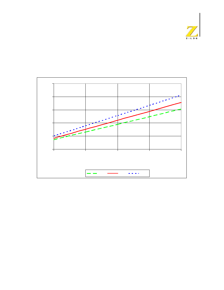
PS019915-1005
Electrical
Characteristics
Z8 Encore!
�
64K Series
Product Specification
215
Figure 45 illustrates the typical current consumption in HALT mode while operating at
25�C versus the system clock frequency. All GPIO pins are configured as outputs and
driven High.
Figure 45. Typical HALT Mode Idd Versus System Clock Frequency
0
1
2
3
4
5
0
5
10
15
20
System Clock Frequency (MHz)
H
A
L
T Id
d (
m
A
)
3.0V
3.3V
3.6V
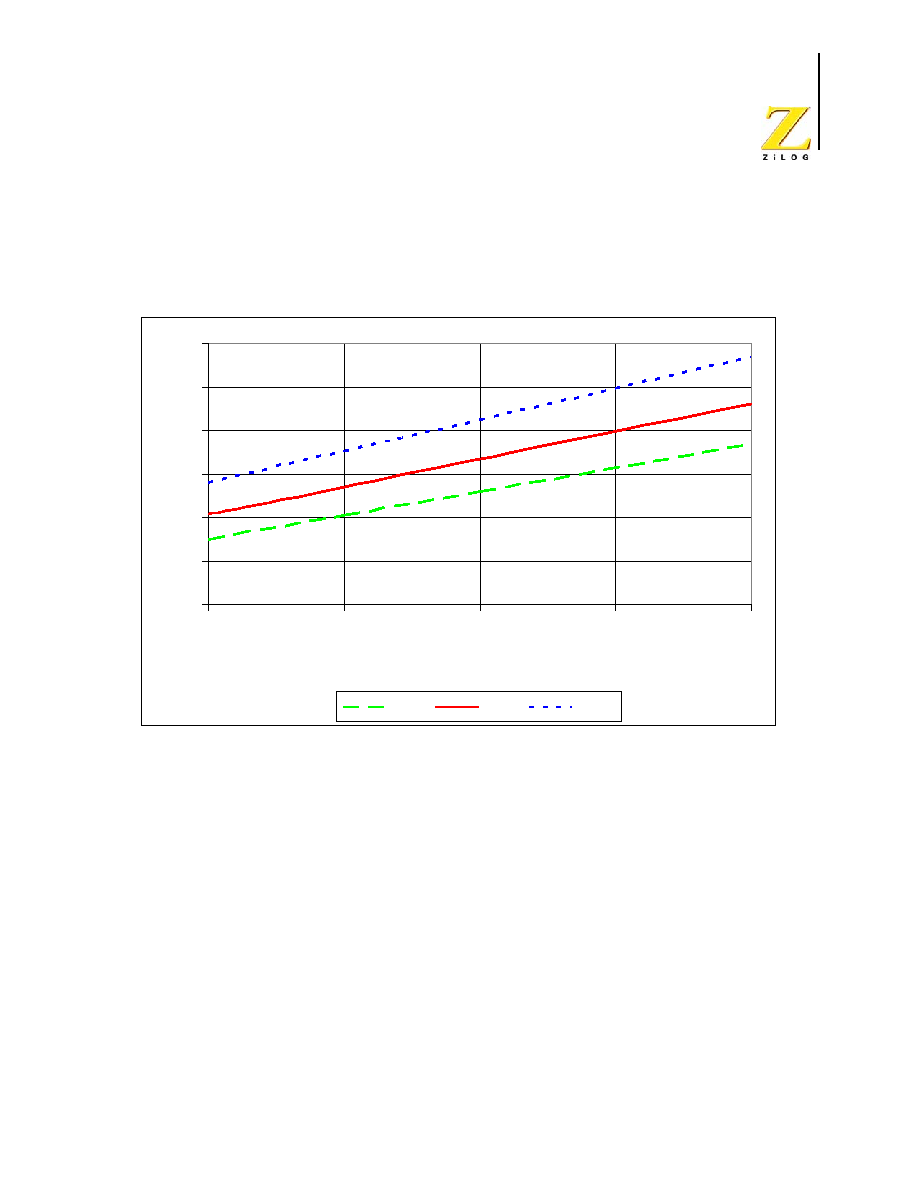
PS019915-1005
Electrical
Characteristics
Z8 Encore!
�
64K Series
Product Specification
216
Figure 45 illustrates the maximum HALT mode current consumption across the full oper-
ating temperature range of the device and versus the system clock frequency. All GPIO
pins are configured as outputs and driven High.
Figure 46. Maximum HALT Mode Icc Versus System Clock Frequency
0
1
2
3
4
5
6
0
5
10
15
20
System Clock Frequency (MHz)
H
a
lt
Id
d
(
m
A
)
3.0V
3.3V
3.6V
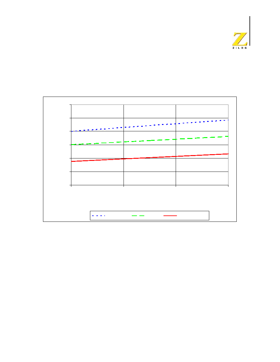
PS019915-1005
Electrical
Characteristics
Z8 Encore!
�
64K Series
Product Specification
217
Figure 47 illustrates the maximum current consumption in STOP mode with the VBO and
Watch-Dog Timer enabled versus the power supply voltage. All GPIO pins are configured
as outputs and driven High.
Figure 47. Maximum STOP Mode Idd with VBO enabled versus Power Supply Voltage
400
450
500
550
600
650
700
3.0
3.2
3.4
3.6
Vdd (V)
S
T
O
P
Idd (
m
ic
r
o
a
m
pe
r
e
s
)
-40/105C
0/70C
25C Typical
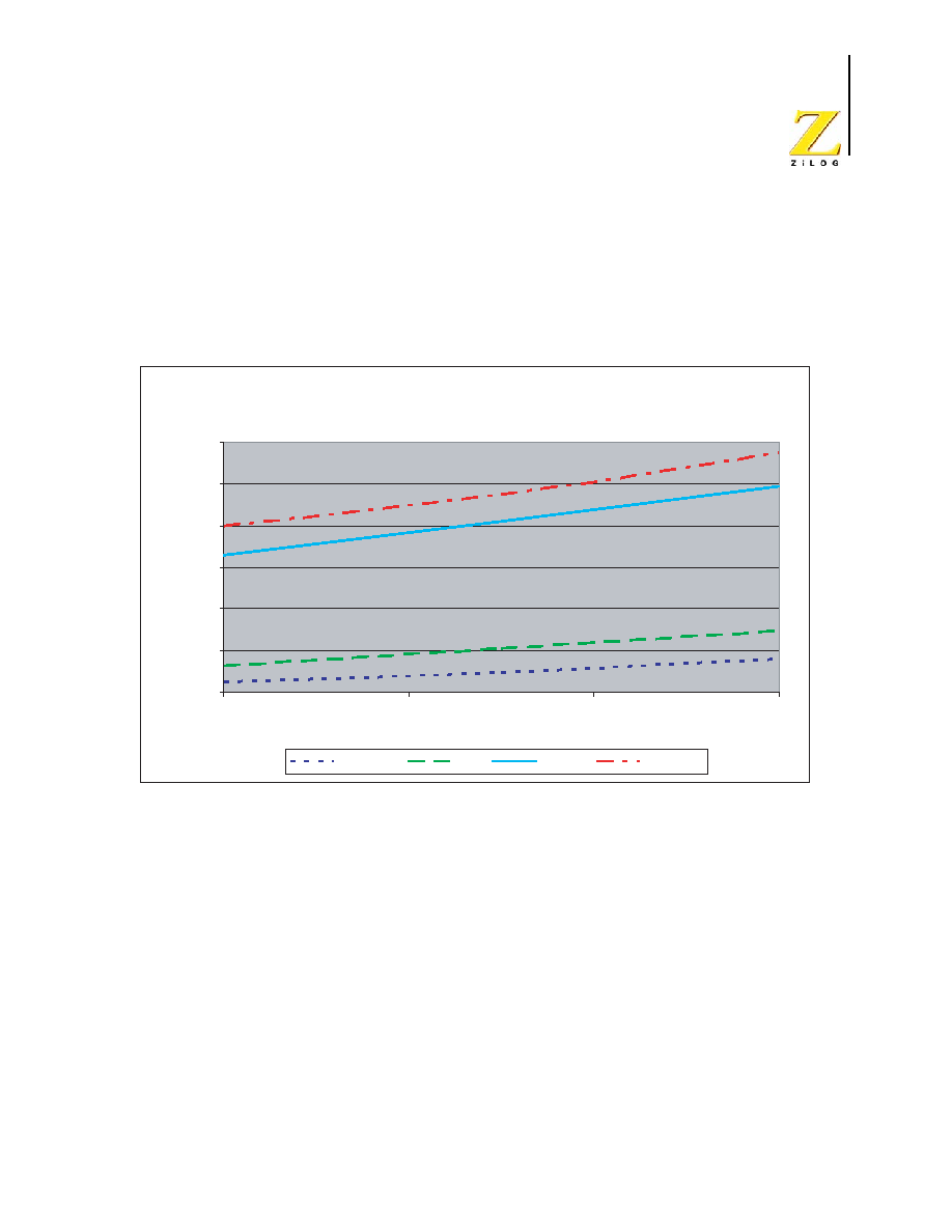
PS019915-1005
Electrical
Characteristics
Z8 Encore!
�
64K Series
Product Specification
218
Figure 48 illustrates the maximum current consumption in STOP mode with the VBO dis-
abled and Watch-Dog Timer enabled versus the power supply voltage. All GPIO pins are
configured as outputs and driven High. Disabling the Watch-Dog Timer and its internal
RC oscillator in STOP mode will provide some additional reduction in STOP mode cur-
rent consumption. This small current reduction would be indistinquishable on the scale of
Figure 48.
Figure 48. Maximum STOP Mode Idd with VBO Disabled versus Power Supply Voltage
0.00
20.00
40.00
60.00
80.00
100.00
120.00
3.0
3.2
3.4
3.6
Vdd (V)
S
T
O
P
Id
d
(
m
icr
o
a
m
p
er
es)
25C Typical
0/70C
-40/105C
-40/+125C
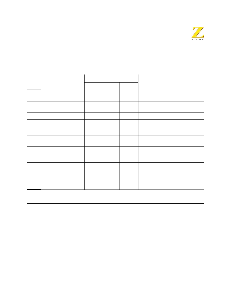
PS019915-1005
Electrical
Characteristics
Z8 Encore!
�
64K Series
Product Specification
219
On-Chip Peripheral AC and DC Electrical Characteristics
Table 106. Power-On Reset and Voltage Brown-Out Electrical Characteristics and Timing
Symbol Parameter
T
A
= �40
0
C to 125
0
C
Units Conditions
Minimum Typical
1
Maximum
V
POR
Power-On Reset Voltage
Threshold
2.40
2.70
2.90
V
V
DD
= V
POR
V
VBO
Voltage Brown-Out Reset
Voltage Threshold
2.30
2.60
2.85
V
V
DD
= V
VBO
V
POR
to V
VBO
hysteresis
50
100
�
mV
Starting V
DD
voltage to
ensure valid Power-On
Reset.
�
V
SS
�
V
T
ANA
Power-On Reset Analog
Delay
�
50
�
s
V
DD
> V
POR
; T
POR
Digital
Reset delay follows T
ANA
T
POR
Power-On Reset Digital
Delay
�
6.6
�
ms
66 WDT Oscillator cycles
(10KHz) + 16 System Clock
cycles (20MHz)
T
VBO
Voltage Brown-Out Pulse
Rejection Period
�
10
�
s
V
DD
< V
VBO
to generate a
Reset.
T
RAMP
Time for VDD to transition
from V
SS
to V
POR
to ensure
valid Reset
0.10
�
100
ms
1 Data in the typical column is from characterization at 3.3V and 0
0
C. These values are provided for design guidance
only and are not tested in production.
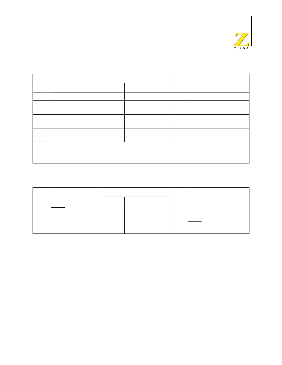
PS019915-1005
Electrical
Characteristics
Z8 Encore!
�
64K Series
Product Specification
220
Table 107. External RC Oscillator Electrical Characteristics and Timing
Symbol Parameter
T
A
= �40
0
C to 125
0
C
Units Conditions
Minimum Typical
1
Maximum
V
DD
Operating Voltage Range
2.70
1
�
�
V
R
EXT
External Resistance from
XIN to VDD
40
45
200
k
V
DD
= V
VBO
C
EXT
External Capacitance from
XIN to VSS
0
20
1000
pF
F
OSC
External RC Oscillation
Frequency
�
�
4
MHz
1 When using the external RC oscillator mode, the oscillator may stop oscillating if the power supply drops below
2.7V, but before the power supply drops to the voltage brown-out threshold. The oscillator will resume oscillation as
soon as the supply voltage exceeds 2.7V.
Table 108. Reset and STOP Mode Recovery Pin Timing
Symbol Parameter
T
A
= �40
0
C to 125
0
C
Units Conditions
Minimum Typical Maximum
T
RESET
RESET pin assertion to
initiate a System Reset.
4
�
�
T
CLK
Not in STOP Mode.
T
CLK
= System Clock period.
T
SMR
STOP Mode Recovery pin
Pulse Rejection Period
10
20
40
ns
RESET, DBG, and GPIO pins
configured as SMR sources.
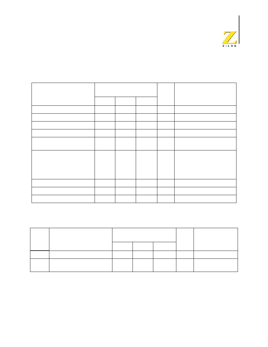
PS019915-1005
Electrical
Characteristics
Z8 Encore!
�
64K Series
Product Specification
221
Table 109 list the Flash Memory electrical characteristics and timing.
Table 110 lists the Watch-Dog Timer electrical characteristics and timing.
Table 109. Flash Memory Electrical Characteristics and Timing
Parameter
V
DD
= 3.0 - 3.6V
T
A
= �40
0
C to 125
0
C
Units Notes
Minimum Typical Maximum
Flash Byte Read Time
50
�
�
ns
Flash Byte Program Time
20
�
40
s
Flash Page Erase Time
10
�
�
ms
Flash Mass Erase Time
200
�
�
ms
Writes to Single Address Before
Next Erase
�
�
2
Flash Row Program Time
�
�
8
ms
Cumulative program time for
single row cannot exceed limit
before next erase. This parameter
is only an issue when bypassing
the Flash Controller.
Data Retention
100
�
�
years
25
0
C
Endurance, �40 to 105
0
C
10,000
�
�
cycles Program / erase cycles
Endurance, 106
0
to 125
0
C
1,000
�
�
cycles Program / erase cycles
Table 110. Watch-Dog Timer Electrical Characteristics and Timing
Symbol Parameter
V
DD
= 3.0 - 3.6V
T
A
= �40
0
C to 125
0
C
Units Conditions
Minimum Typical
Maximum
F
WDT
WDT Oscillator Frequency
5
10
20
kHz
I
WDT
WDT Oscillator Current including
internal RC oscillator
�
< 1
5
A
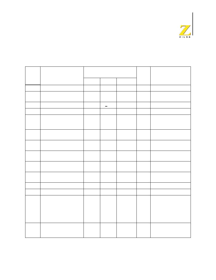
PS019915-1005
Electrical
Characteristics
Z8 Encore!
�
64K Series
Product Specification
222
Table 111 provides electrical characteristics and timing information for the Analog-to-Digital Converter.
Figure 49 illustrates the input frequency response of the ADC.
Table 111. Analog-to-Digital Converter Electrical Characteristics and Timing
Symbol Parameter
V
DD
= 3.0 - 3.6V
T
A
= �40
0
C to 125
0
C
Units Conditions
Minimum Typical
Maximum
Resolution
10
�
�
bits
External V
REF
= 3.0V;
Differential Nonlinearity
(DNL)
-.25
+.25
lsb
Guaranteed by design
Integral Nonlinearity (INL)
-3.0
+1.0
3.0
lsb
External V
REF
= 3.0V
DC Offset Error
-35
�
25
mV
DC Offset Error
-50
�
25
mV
44-pin LQFP, 44-pin
PLCC, and 68-pin PLCC
packages.
V
REF
Internal Reference Voltage
1.9
2.0
2.4
V
V
DD
= 3.0 - 3.6V
T
A
= -40
0
C to 105
0
C
VC
REF
Voltage Coefficient of
Internal Reference Voltage
�
78
�
mV/V
V
REF
variation as a
function of AVDD.
TC
REF
Temperature Coefficient of
Internal Reference Voltage
�
1
�
mV/
0
C
Single-Shot Conversion
Period
�
5129
�
cycles
System clock cycles
Continuous Conversion
Period
�
256
�
cycles
System clock cycles
R
S
Analog Source Impedance
�
�
150
Recommended
Zin
Input Impedance
150
k
V
REF
External Reference Voltage
AVDD
V
AVDD <= VDD. When
using an external reference
voltage, decoupling
capacitance should be
placed from VREF to
AVSS.
I
REF
Current draw into VREF pin
when driving with external
source.
25.0
40.0
A
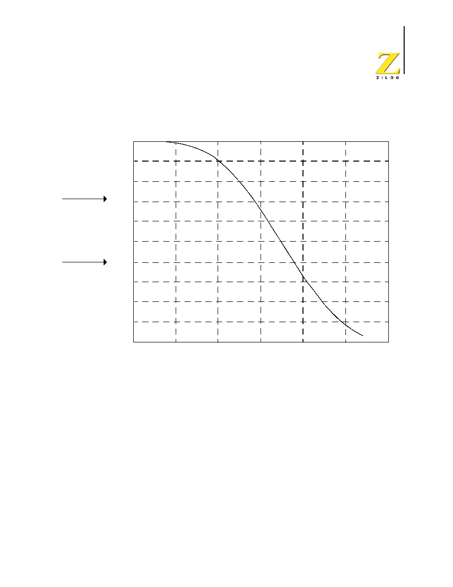
PS019915-1005
Electrical
Characteristics
Z8 Encore!
�
64K Series
Product Specification
223
Figure 49. Analog-to-Digital Converter Frequency Response
Frequency (kHz)
0.9
0.8
0.7
0.6
0.3
0.4
0.2
0.1
0
Fr
eq
ue
ncy Respo
n
se
1
0.5
0
5
10
15
20
25
30
-6 dB
-3 dB
ADC Magnitude Transfer Function (Linear Scale)
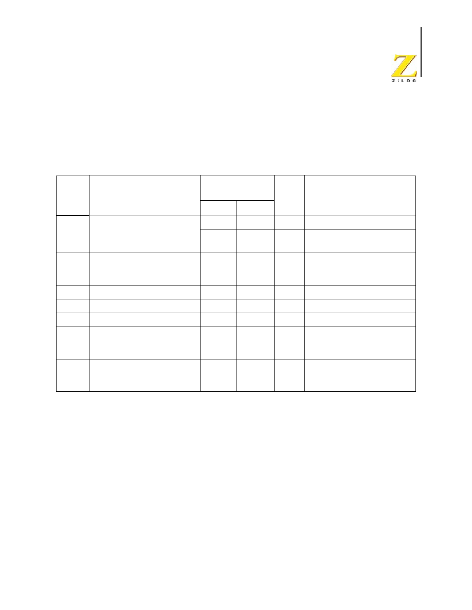
PS019915-1005
Electrical
Characteristics
Z8 Encore!
�
64K Series
Product Specification
224
AC Characteristics
The section provides information on the AC characteristics and timing. All AC timing
information assumes a standard load of 50pF on all outputs. Table 112 lists the 64K Series
AC characteristics and timing.
Table 112. AC Characteristics
Symbol Parameter
V
DD
= 3.0 - 3.6V
T
A
= �40
0
C to 125
0
C
Units Conditions
Minimum Maximum
F
sysclk
System Clock Frequency
�
20.0
MHz
Read-only from Flash memory.
0.032768
20.0
MHz
Program or erasure of the Flash
memory.
F
XTAL
Crystal Oscillator Frequency
0.032768
20.0
MHz
System clock frequencies below
the crystal oscillator minimum
require an external clock driver.
T
XIN
Crystal Oscillator Clock Period
50
�
ns
T
CLK
= 1/F
sysclk
T
XINH
System Clock High Time
20
ns
T
XINL
System Clock Low Time
20
ns
T
XINR
System Clock Rise Time
�
3
ns
T
CLK
= 50ns. Slower rise times
can be tolerated with longer clock
periods.
T
XINF
System Clock Fall Time
�
3
ns
T
CLK
= 50ns. Slower fall times can
be tolerated with longer clock
periods.
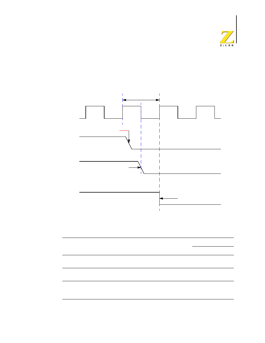
PS019915-1005
Electrical
Characteristics
Z8 Encore!
�
64K Series
Product Specification
225
General Purpose I/O Port Input Data Sample Timing
Figure 50 illustrates timing of the GPIO Port input sampling. Table 113 lists the GPIO port
input timing.
Figure 50. Port Input Sample Timing
Table 113. GPIO Port Input Timing
Parameter
Abbreviation
Delay (ns)
Min
Max
T
S_PORT
Port Input Transition to XIN Fall Setup Time
(Not pictured)
5
�
T
H_PORT
XIN Fall to Port Input Transition Hold Time
(Not pictured)
6
�
T
SMR
GPIO Port Pin Pulse Width to Insure STOP Mode
Recovery
(for GPIO Port Pins enabled as SMR sources)
1
s
System
TCLK
GPIO Pin
Port Value
Changes to 0
0 Latched
Into Port Input
Input Value
GPIO Input
Data Latch
Clock
Data Register
GPIO Data
Read on Data Bus
GPIO Data Register
Value 0 Read
by eZ8 CPU
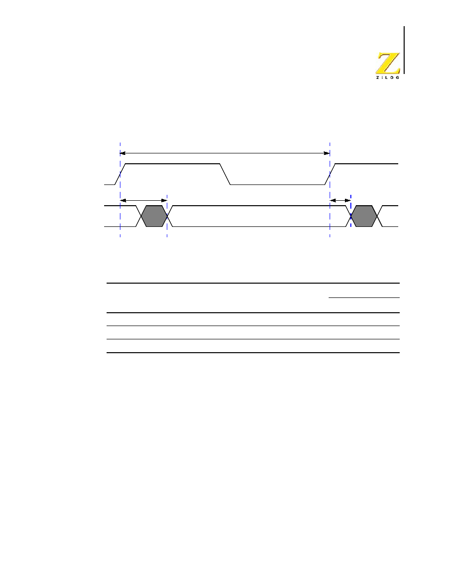
PS019915-1005
Electrical
Characteristics
Z8 Encore!
�
64K Series
Product Specification
226
General Purpose I/O Port Output Timing
Figure 51 and Table 114 provide timing information for GPIO Port pins.
Figure 51. GPIO Port Output Timing
Table 114. GPIO Port Output Timing
Parameter
Abbreviation
Delay (ns)
Min
Max
GPIO Port pins
T
1
XIN Rise to Port Output Valid Delay
�
20
T
2
XIN Rise to Port Output Hold Time
2
�
XIN
Port Output
TCLK
T1
T2
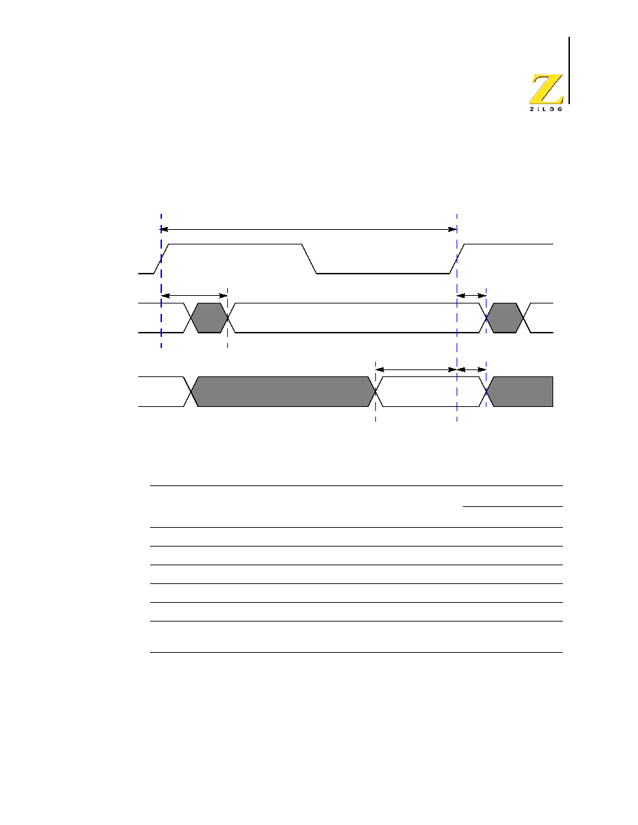
PS019915-1005
Electrical
Characteristics
Z8 Encore!
�
64K Series
Product Specification
227
On-Chip Debugger Timing
Figure 52 and Table 115 provide timing information for the DBG pin. The DBG pin tim-
ing specifications assume a 4
s maximum rise and fall time.
Figure 52. On-Chip Debugger Timing
Table 115. On-Chip Debugger Timing
Parameter
Abbreviation
Delay (ns)
Min
Max
DBG
T
1
XIN Rise to DBG Valid Delay
�
30
T
2
XIN Rise to DBG Output Hold Time
2
�
T
3
DBG to XIN Rise Input Setup Time
10
�
T
4
DBG to XIN Rise Input Hold Time
5
�
DBG frequency
System
Clock / 4
XIN
DBG
TCLK
T1
T2
(Output)
DBG
T3
T4
(Input)
Output Data
Input Data
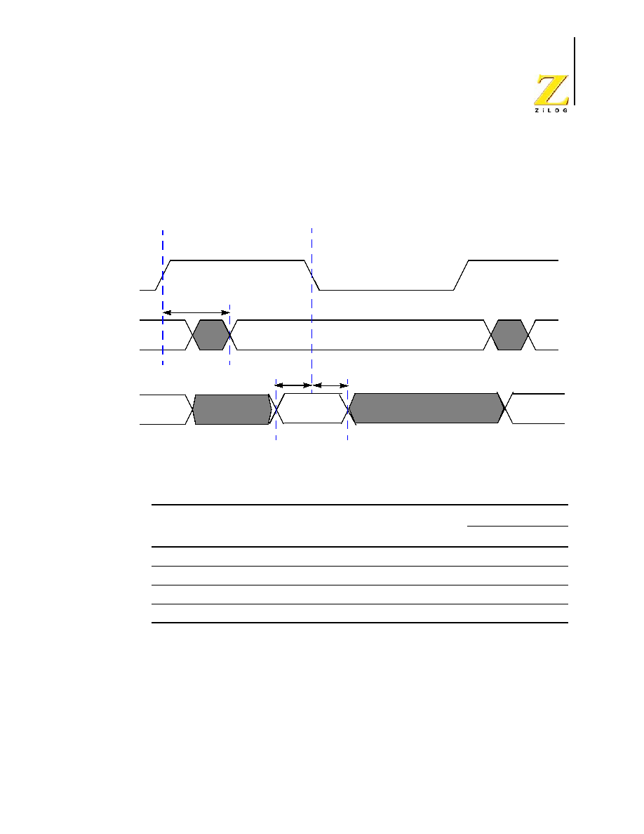
PS019915-1005
Electrical
Characteristics
Z8 Encore!
�
64K Series
Product Specification
228
SPI Master Mode Timing
Figure 53 and Table 116 provide timing information for SPI Master mode pins. Timing is
shown with SCK rising edge used to source MOSI output data, SCK falling edge used to
sample MISO input data. Timing on the SS output pin(s) is controlled by software.
Figure 53. SPI Master Mode Timing
Table 116. SPI Master Mode Timing
Parameter
Abbreviation
Delay (ns)
Min
Max
SPI Master
T
1
SCK Rise to MOSI output Valid Delay
-5
+5
T
2
MISO input to SCK (receive edge) Setup Time
20
T
3
MISO input to SCK (receive edge) Hold Time
0
SCK
MOSI
T1
(Output)
MISO
T2
T3
(Input)
Output Data
Input Data
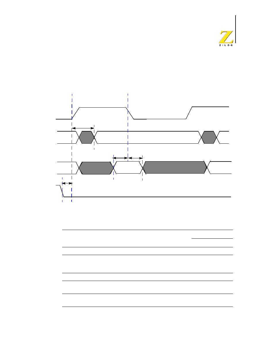
PS019915-1005
Electrical
Characteristics
Z8 Encore!
�
64K Series
Product Specification
229
SPI Slave Mode Timing
Figure 54 and Table 117 provide timing information for the SPI slave mode pins. Timing
is shown with SCK rising edge used to source MISO output data, SCK falling edge used to
sample MOSI input data.
Figure 54. SPI Slave Mode Timing
Table 117. SPI Slave Mode Timing
Parameter
Abbreviation
Delay (ns)
Min
Max
SPI Slave
T
1
SCK (transmit edge) to MISO output Valid Delay
2 * Xin
period
3 * Xin
period +
20 nsec
T
2
MOSI input to SCK (receive edge) Setup Time
0
T
3
MOSI input to SCK (receive edge) Hold Time
3 * Xin
period
T
4
SS input assertion to SCK setup
1 * Xin
period
SCK
MISO
T1
(Output)
MOSI
T2
T3
(Input)
Output Data
Input Data
SS
(Input)
T4
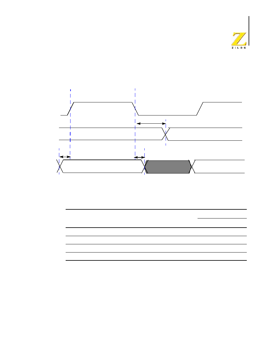
PS019915-1005
Electrical
Characteristics
Z8 Encore!
�
64K Series
Product Specification
230
I
2
C Timing
Figure 55 and Table 118 provide timing information for I
2
C pins.
Figure 55. I
2
C Timing
Table 118. I
2
C Timing
Parameter
Abbreviation
Delay (ns)
Minimum Maximum
I
2
C
T
1
SCL Fall to SDA output delay
SCL period/4
T
2
SDA Input to SCL rising edge Setup Time
0
T
3
SDA Input to SCL falling edge Hold Time
0
SCL
SDA
T1
(Output)
SDA
T2
(Input)
Output Data
Input Data
(Output)
T3
PS019915-1005
Electrical
Characteristics
Z8 Encore!
�
64K Series
Product Specification
231
UART Timing
Figure 56 and Table 119 provide timing information for UART pins for the case where the
Clear To Send input pin (CTS) is used for flow control. In this example, it is assumed that
the Driver Enable polarity has been configured to be Active Low and is represented here
by DE. The CTS to DE assertion delay (T1) assumes the UART Transmit Data register has
been loaded with data prior to CTS assertion.
Figure 56. UART Timing with CTS
Table 119. UART Timing with CTS
Parameter Abbreviation
Delay (ns)
Minimum
Maximum
T
1
CTS Fall to DE Assertion Delay
2 * XIN period 2 * XIN period
+ 1 Bit period
T
2
DE Assertion to TXD Falling Edge (Start) Delay 1 Bit period
1 Bit period +
1 * XIN period
T
3
End of Stop Bit(s) to DE Deassertion Delay
1 * XIN period 2 * XIN period
T
1
T
2
TXD
(Output)
DE
(Output)
CTS
(Input)
Start
Bit 0
T
3
Bit 7
Parity
Stop
Bit 1
End of
Stop Bit(s)
PS019915-1005
Electrical
Characteristics
Z8 Encore!
�
64K Series
Product Specification
232
Figure 57 and Table 120 provide timing information for UART pins for the case where the
Clear To Send input signal (CTS) is not used for flow control. In this example, it is
assumed that the Driver Enable polarity has been configured to be Active Low and is rep-
resented here by DE. DE asserts after the UART Transmit Data Register has been written.
DE remains asserted for multiple characters as long as the Transmit Data register is writ-
ten with the next character before the current character has completed.
Figure 57. UART Timing without CTS
Table 120. UART Timing without CTS
Parameter Abbreviation
Delay (ns)
Minimum
Maximum
T
1
DE Assertion to TXD Falling Edge (Start) Delay
1 Bit period
1 Bit period +
1 * XIN period
T
2
End of Stop Bit(s) to DE Deassertion Delay
1 * XIN period
2 * XIN period
T
1
TXD
(Output)
DE
(Output)
Start
Bit 0
T
2
Bit 7
Parity
Stop
Bit 1
End of
Stop Bit(s)

Z8 Encore!
�
64K Series
Product Specification
PS019915-1005
eZ8 CPU Instruction Set
233
eZ8 CPU Instruction Set
Assembly Language Programming Introduction
The eZ8 CPU assembly language provides a means for writing an application program
without having to be concerned with actual memory addresses or machine instruction for-
mats. A program written in assembly language is called a source program. Assembly lan-
guage allows the use of symbolic addresses to identify memory locations. It also allows
mnemonic codes (opcodes and operands) to represent the instructions themselves. The
opcodes identify the instruction while the operands represent memory locations, registers,
or immediate data values.
Each assembly language program consists of a series of symbolic commands called state-
ments. Each statement can contain labels, operations, operands and comments.
Labels can be assigned to a particular instruction step in a source program. The label iden-
tifies that step in the program as an entry point for use by other instructions.
The assembly language also includes assembler directives that supplement the machine
instruction. The assembler directives, or pseudo-ops, are not translated into a machine
instruction. Rather, the pseudo-ops are interpreted as directives that control or assist the
assembly process.
The source program is processed (assembled) by the assembler to obtain a machine lan-
guage program called the object code. The object code is executed by the eZ8 CPU. An
example segment of an assembly language program is detailed in the following example.
Assembly Language Source Program Example
JP START
; Everything after the semicolon is a comment.
START:
; A label called "START". The first instruction (
JP START
) in this
; example causes program execution to jump to the point within the
; program where the
START
label occurs.
LD R4, R7
; A Load (LD) instruction with two operands. The first operand,
; Working Register R4, is the destination. The second operand,
; Working Register R7, is the source. The contents of R7 is
; written into R4.
LD 234H, #%01
; Another Load (LD) instruction with two operands.
; The first operand, Extended Mode Register Address
234H
,
; identifies the destination. The second operand, Immediate Data

PS019915-1005
eZ8 CPU Instruction Set
Z8 Encore!
�
64K Series
Product Specification
234
; value
01H
, is the source. The value
01H
is written into the
; Register at address
234H
.
Assembly Language Syntax
For proper instruction execution, eZ8 CPU assembly language syntax requires that the
operands be written as `destination, source'. After assembly, the object code usually has
the operands in the order 'source, destination', but ordering is opcode-dependent. The fol-
lowing instruction examples illustrate the format of some basic assembly instructions and
the resulting object code produced by the assembler. This binary format must be followed
by users that prefer manual program coding or intend to implement their own assembler.
Example 1: If the contents of Registers 43H and 08H are added and the result is stored in
43H, the assembly syntax and resulting object code is:
Example 2: In general, when an instruction format requires an 8-bit register address, that
address can specify any register location in the range 0 - 255 or, using Escaped Mode
Addressing, a Working Register R0 - R15. If the contents of Register 43H and Working
Register R8 are added and the result is stored in 43H, the assembly syntax and resulting
object code is:
See the device-specific Product Specification to determine the exact register file range
available. The register file size varies, depending on the device type.
eZ8 CPU Instruction Notation
In the eZ8 CPU Instruction Summary and Description sections, the operands, condition
codes, status flags, and address modes are represented by a notational shorthand that is
described in Table 121.
Assembly Language Syntax Example 1
Assembly Language Code ADD
43H,
08H
(ADD dst, src)
Object Code
04
08
43
(OPC src, dst)
Assembly Language Syntax Example 2
Assembly Language Code ADD
43H,
R8
(ADD dst, src)
Object Code
04
E8
43
(OPC src, dst)

PS019915-1005
eZ8 CPU Instruction Set
Z8 Encore!
�
64K Series
Product Specification
235
.
Table 122 contains additional symbols that are used throughout the Instruction Summary
and Instruction Set Description sections.
Table 121. Notational Shorthand
Notation Description
Operand Range
b
Bit
b
b represents a value from 0 to 7 (000B to 111B).
cc
Condition Code
--
See Condition Codes overview in the eZ8 CPU User
Manual.
DA
Direct Address
Addrs
Addrs. represents a number in the range of 0000H to
FFFFH
ER
Extended Addressing Register
Reg
Reg. represents a number in the range of 000H to
FFFH
IM
Immediate Data
#Data
Data is a number between 00H to FFH
Ir
Indirect Working Register
@Rn
n = 0 �15
IR
Indirect Register
@Reg
Reg. represents a number in the range of 00H to FFH
Irr
Indirect Working Register Pair
@RRp
p = 0, 2, 4, 6, 8, 10, 12, or 14
IRR
Indirect Register Pair
@Reg
Reg. represents an even number in the range 00H to
FEH
p
Polarity
p
Polarity is a single bit binary value of either 0B or 1B.
r
Working Register
Rn
n = 0 � 15
R
Register
Reg
Reg. represents a number in the range of 00H to FFH
RA
Relative Address
X
X represents an index in the range of +127 to �128
which is an offset relative to the address of the next
instruction
rr
Working Register Pair
RRp
p = 0, 2, 4, 6, 8, 10, 12, or 14
RR
Register Pair
Reg
Reg. represents an even number in the range of 00H to
FEH
Vector
Vector Address
Vector
Vector represents a number in the range of 00H to FFH
X
Indexed
#Index
The register or register pair to be indexed is offset by
the signed Index value (#Index) in a +127 to -128
range.

PS019915-1005
eZ8 CPU Instruction Set
Z8 Encore!
�
64K Series
Product Specification
236
Assignment of a value is indicated by an arrow. For example,
dst
dst + src
indicates the source data is added to the destination data and the result is stored in the des-
tination location.
Table 122. Additional Symbols
Symbol
Definition
dst
Destination Operand
src
Source Operand
@
Indirect Address Prefix
SP
Stack Pointer
PC
Program Counter
FLAGS
Flags Register
RP
Register Pointer
#
Immediate Operand Prefix
B
Binary Number Suffix
%
Hexadecimal Number Prefix
H
Hexadecimal Number Suffix

PS019915-1005
eZ8 CPU Instruction Set
Z8 Encore!
�
64K Series
Product Specification
237
Condition Codes
The C, Z, S and V flags control the operation of the conditional jump (JP cc and JR cc)
instructions. Sixteen frequently useful functions of the flag settings are encoded in a 4-bit
field called the condition code (cc), which forms Bits 7:4 of the conditional jump instruc-
tions. The condition codes are summarized in Table 123. Some binary condition codes can
be created using more than one assembly code mnemonic. The result of the flag test oper-
ation decides if the conditional jump is executed.
Table 123. Condition Codes
Binary
Hex
Assembly
Mnemonic Definition
Flag Test Operation
0000
0
F
Always False
�
0001
1
LT
Less Than
(S XOR V) = 1
0010
2
LE
Less Than or Equal
(Z OR (S XOR V)) = 1
0011
3
ULE
Unsigned Less Than or Equal
(C OR Z) = 1
0100
4
OV
Overflow
V = 1
0101
5
Ml
Minus
S = 1
0110
6
Z
Zero
Z = 1
0110
6
EQ
Equal
Z = 1
0111
7
C
Carry
C = 1
0111
7
ULT
Unsigned Less Than
C = 1
1000
8
T (or blank) Always True
�
1001
9
GE
Greater Than or Equal
(S XOR V) = 0
1010
A
GT
Greater Than
(Z OR (S XOR V)) = 0
1011
B
UGT
Unsigned Greater Than
(C = 0 AND Z = 0) = 1
1100
C
NOV
No Overflow
V = 0
1101
D
PL
Plus
S = 0
1110
E
NZ
Non-Zero
Z = 0
1110
E
NE
Not Equal
Z = 0
1111
F
NC
No Carry
C = 0
1111
F
UGE
Unsigned Greater Than or Equal C = 0

PS019915-1005
eZ8 CPU Instruction Set
Z8 Encore!
�
64K Series
Product Specification
238
eZ8 CPU Instruction Classes
eZ8 CPU instructions can be divided functionally into the following groups:
�
Arithmetic
�
Bit Manipulation
�
Block Transfer
�
CPU Control
�
Load
�
Logical
�
Program Control
�
Rotate and Shift
Tables 124 through 131 contain the instructions belonging to each group and the number
of operands required for each instruction. Some instructions appear in more than one table
as these instruction can be considered as a subset of more than one category. Within these
tables, the source operand is identified as 'src', the destination operand is 'dst' and a con-
dition code is 'cc'.
Table 124. Arithmetic Instructions
Mnemonic
Operands
Instruction
ADC
dst, src
Add with Carry
ADCX
dst, src
Add with Carry using Extended Addressing
ADD
dst, src
Add
ADDX
dst, src
Add using Extended Addressing
CP
dst, src
Compare
CPC
dst, src
Compare with Carry
CPCX
dst, src
Compare with Carry using Extended Addressing
CPX
dst, src
Compare using Extended Addressing
DA
dst
Decimal Adjust
DEC
dst
Decrement
DECW
dst
Decrement Word
INC
dst
Increment
INCW
dst
Increment Word
MULT
dst
Multiply

PS019915-1005
eZ8 CPU Instruction Set
Z8 Encore!
�
64K Series
Product Specification
239
SBC
dst, src
Subtract with Carry
SBCX
dst, src
Subtract with Carry using Extended Addressing
SUB
dst, src
Subtract
SUBX
dst, src
Subtract using Extended Addressing
Table 125. Bit Manipulation Instructions
Mnemonic
Operands
Instruction
BCLR
bit, dst
Bit Clear
BIT
p, bit, dst
Bit Set or Clear
BSET
bit, dst
Bit Set
BSWAP
dst
Bit Swap
CCF
--
Complement Carry Flag
RCF
--
Reset Carry Flag
SCF
--
Set Carry Flag
TCM
dst, src
Test Complement Under Mask
TCMX
dst, src
Test Complement Under Mask using Extended Addressing
TM
dst, src
Test Under Mask
TMX
dst, src
Test Under Mask using Extended Addressing
Table 126. Block Transfer Instructions
Mnemonic
Operands
Instruction
LDCI
dst, src
Load Constant to/from Program Memory and Auto-Increment
Addresses
LDEI
dst, src
Load External Data to/from Data Memory and Auto-Increment
Addresses
Table 124. Arithmetic Instructions (Continued)
Mnemonic
Operands
Instruction

PS019915-1005
eZ8 CPU Instruction Set
Z8 Encore!
�
64K Series
Product Specification
240
Table 127. CPU Control Instructions
Mnemonic
Operands
Instruction
ATM
--
Atomic Execution
CCF
--
Complement Carry Flag
DI
--
Disable Interrupts
EI
--
Enable Interrupts
HALT
--
HALT Mode
NOP
--
No Operation
RCF
--
Reset Carry Flag
SCF
--
Set Carry Flag
SRP
src
Set Register Pointer
STOP
--
STOP Mode
WDT
--
Watch-Dog Timer Refresh
Table 128. Load Instructions
Mnemonic Operands Instruction
CLR
dst
Clear
LD
dst, src
Load
LDC
dst, src
Load Constant to/from Program Memory
LDCI
dst, src
Load Constant to/from Program Memory and Auto-Increment
Addresses
LDE
dst, src
Load External Data to/from Data Memory
LDEI
dst, src
Load External Data to/from Data Memory and Auto-Increment
Addresses
LDWX
dst, src
Load Word using Extended Addressing
LDX
dst, src
Load using Extended Addressing
LEA
dst, X(src) Load Effective Address
POP
dst
Pop
POPX
dst
Pop using Extended Addressing
PUSH
src
Push
PUSHX
src
Push using Extended Addressing

PS019915-1005
eZ8 CPU Instruction Set
Z8 Encore!
�
64K Series
Product Specification
241
Table 129. Logical Instructions
Mnemonic Operands Instruction
AND
dst, src
Logical AND
ANDX
dst, src
Logical AND using Extended Addressing
COM
dst
Complement
OR
dst, src
Logical OR
ORX
dst, src
Logical OR using Extended Addressing
XOR
dst, src
Logical Exclusive OR
XORX
dst, src
Logical Exclusive OR using Extended Addressing
Table 130. Program Control Instructions
Mnemonic
Operands
Instruction
BRK
--
On-Chip Debugger Break
BTJ
p, bit, src, DA Bit Test and Jump
BTJNZ
bit, src, DA
Bit Test and Jump if Non-Zero
BTJZ
bit, src, DA
Bit Test and Jump if Zero
CALL
dst
Call Procedure
DJNZ
dst, src, RA
Decrement and Jump Non-Zero
IRET
--
Interrupt Return
JP
dst
Jump
JP cc
dst
Jump Conditional
JR
DA
Jump Relative
JR cc
DA
Jump Relative Conditional
RET
--
Return
TRAP
vector
Software Trap

PS019915-1005
eZ8 CPU Instruction Set
Z8 Encore!
�
64K Series
Product Specification
242
eZ8 CPU Instruction Summary
Table 132 summarizes the eZ8 CPU instructions. The table identifies the addressing
modes employed by the instruction, the effect upon the Flags register, the number of CPU
clock cycles required for the instruction fetch, and the number of CPU clock cycles
required for the instruction execution.
.
Table 131. Rotate and Shift Instructions
Mnemonic
Operands
Instruction
BSWAP
dst
Bit Swap
RL
dst
Rotate Left
RLC
dst
Rotate Left through Carry
RR
dst
Rotate Right
RRC
dst
Rotate Right through Carry
SRA
dst
Shift Right Arithmetic
SRL
dst
Shift Right Logical
SWAP
dst
Swap Nibbles
Table 132. eZ8 CPU Instruction Summary
Assembly
Mnemonic
Symbolic Operation
Address Mode
Opcode(s)
(Hex)
Flags
Fetch
Cycles
Instr.
Cycles
dst
src
C Z S V D H
ADC dst, src
dst
dst + src + C
r
r
12
*
*
*
*
0
*
2
3
r
Ir
13
2
4
R
R
14
3
3
R
IR
15
3
4
R
IM
16
3
3
IR
IM
17
3
4
ADCX dst, src
dst
dst + src + C
ER
ER
18
*
*
*
*
0
*
4
3
ER
IM
19
4
3
Flags Notation:
* = Value is a function of the result of the operation.
- = Unaffected
X = Undefined
0 = Reset to 0
1 = Set to 1
PS019915-1005
eZ8 CPU Instruction Set
Z8 Encore!
�
64K Series
Product Specification
243
ADD dst, src
dst
dst + src
r
r
02
*
*
*
*
0
*
2
3
r
Ir
03
2
4
R
R
04
3
3
R
IR
05
3
4
R
IM
06
3
3
IR
IM
07
3
4
ADDX dst, src
dst
dst + src
ER
ER
08
*
*
*
*
0
*
4
3
ER
IM
09
4
3
AND dst, src
dst
dst AND src
r
r
52
-
*
*
0
-
-
2
3
r
Ir
53
2
4
R
R
54
3
3
R
IR
55
3
4
R
IM
56
3
3
IR
IM
57
3
4
ANDX dst, src
dst
dst AND src
ER
ER
58
-
*
*
0
-
-
4
3
ER
IM
59
4
3
ATM
Block all interrupt and
DMA requests during
execution of the next 3
instructions
2F
-
-
-
-
-
-
1
2
BCLR bit, dst
dst[bit]
0
r
E2
-
*
*
0
-
-
2
2
BIT p, bit, dst
dst[bit]
p
r
E2
-
*
*
0
-
-
2
2
BRK
Debugger Break
00
-
-
-
-
-
-
1
1
BSET bit, dst
dst[bit]
1
r
E2
-
*
*
0
-
-
2
2
BSWAP dst
dst[7:0]
dst[0:7]
R
D5
X *
*
0
-
-
2
2
BTJ p, bit, src, dst if src[bit] = p
PC
PC + X
r
F6
-
-
-
-
-
-
3
3
Ir
F7
3
4
Table 132. eZ8 CPU Instruction Summary (Continued)
Assembly
Mnemonic
Symbolic Operation
Address Mode
Opcode(s)
(Hex)
Flags
Fetch
Cycles
Instr.
Cycles
dst
src
C Z S V D H
Flags Notation:
* = Value is a function of the result of the operation.
- = Unaffected
X = Undefined
0 = Reset to 0
1 = Set to 1

PS019915-1005
eZ8 CPU Instruction Set
Z8 Encore!
�
64K Series
Product Specification
244
BTJNZ bit, src, dst if src[bit] = 1
PC
PC + X
r
F6
-
-
-
-
-
-
3
3
Ir
F7
3
4
BTJZ bit, src, dst
if src[bit] = 0
PC
PC + X
r
F6
-
-
-
-
-
-
3
3
Ir
F7
3
4
CALL dst
SP
SP -2
@SP
PC
PC
dst
IRR
D4
-
-
-
-
-
-
2
6
DA
D6
3
3
CCF
C
~C
EF
*
-
-
-
-
-
1
2
CLR dst
dst
00H
R
B0
-
-
-
-
-
-
2
2
IR
B1
2
3
COM dst
dst
~dst
R
60
-
*
*
0
-
-
2
2
IR
61
2
3
CP dst, src
dst - src
r
r
A2
*
*
*
*
-
-
2
3
r
Ir
A3
2
4
R
R
A4
3
3
R
IR
A5
3
4
R
IM
A6
3
3
IR
IM
A7
3
4
CPC dst, src
dst - src - C
r
r
1F A2
*
*
*
*
-
-
3
3
r
Ir
1F A3
3
4
R
R
1F A4
4
3
R
IR
1F A5
4
4
R
IM
1F A6
4
3
IR
IM
1F A7
4
4
CPCX dst, src
dst - src - C
ER
ER
1F A8
*
*
*
*
-
-
5
3
ER
IM
1F A9
5
3
Table 132. eZ8 CPU Instruction Summary (Continued)
Assembly
Mnemonic
Symbolic Operation
Address Mode
Opcode(s)
(Hex)
Flags
Fetch
Cycles
Instr.
Cycles
dst
src
C Z S V D H
Flags Notation:
* = Value is a function of the result of the operation.
- = Unaffected
X = Undefined
0 = Reset to 0
1 = Set to 1

PS019915-1005
eZ8 CPU Instruction Set
Z8 Encore!
�
64K Series
Product Specification
245
CPX dst, src
dst - src
ER
ER
A8
*
*
*
*
-
-
4
3
ER
IM
A9
4
3
DA dst
dst
DA(dst)
R
40
*
*
* X
-
-
2
2
IR
41
2
3
DEC dst
dst
dst - 1
R
30
-
*
*
*
-
-
2
2
IR
31
2
3
DECW dst
dst
dst - 1
RR
80
-
*
*
*
-
-
2
5
IRR
81
2
6
DI
IRQCTL[7]
0
8F
-
-
-
-
-
-
1
2
DJNZ dst, RA
dst
dst � 1
if dst
0
PC
PC + X
r
0A-FA
-
-
-
-
-
-
2
3
EI
IRQCTL[7]
1
9F
-
-
-
-
-
-
1
2
HALT
HALT Mode
7F
-
-
-
-
-
-
1
2
INC dst
dst
dst + 1
R
20
-
*
*
*
-
-
2
2
IR
21
2
3
r
0E-FE
1
2
INCW dst
dst
dst + 1
RR
A0
-
*
*
*
-
-
2
5
IRR
A1
2
6
IRET
FLAGS
@SP
SP
SP + 1
PC
@SP
SP
SP + 2
IRQCTL[7]
1
BF
*
*
*
*
*
*
1
5
JP dst
PC
dst
DA
8D
-
-
-
-
-
-
3
2
IRR
C4
2
3
JP cc, dst
if cc is true
PC
dst
DA
0D-FD
-
-
-
-
-
-
3
2
Table 132. eZ8 CPU Instruction Summary (Continued)
Assembly
Mnemonic
Symbolic Operation
Address Mode
Opcode(s)
(Hex)
Flags
Fetch
Cycles
Instr.
Cycles
dst
src
C Z S V D H
Flags Notation:
* = Value is a function of the result of the operation.
- = Unaffected
X = Undefined
0 = Reset to 0
1 = Set to 1

PS019915-1005
eZ8 CPU Instruction Set
Z8 Encore!
�
64K Series
Product Specification
246
JR dst
PC
PC + X
DA
8B
-
-
-
-
-
-
2
2
JR cc, dst
if cc is true
PC
PC + X
DA
0B-FB
-
-
-
-
-
-
2
2
LD dst, rc
dst
src
r
IM
0C-FC
-
-
-
-
-
-
2
2
r
X(r)
C7
3
3
X(r)
r
D7
3
4
r
Ir
E3
2
3
R
R
E4
3
2
R
IR
E5
3
4
R
IM
E6
3
2
IR
IM
E7
3
3
Ir
r
F3
2
3
IR
R
F5
3
3
LDC dst, src
dst
src
r
Irr
C2
-
-
-
-
-
-
2
5
Ir
Irr
C5
2
9
Irr
r
D2
2
5
LDCI dst, src
dst
src
r
r + 1
rr
rr + 1
Ir
Irr
C3
-
-
-
-
-
-
2
9
Irr
Ir
D3
2
9
LDE dst, src
dst
src
r
Irr
82
-
-
-
-
-
-
2
5
Irr
r
92
2
5
LDEI dst, src
dst
src
r
r + 1
rr
rr + 1
Ir
Irr
83
-
-
-
-
-
-
2
9
Irr
Ir
93
2
9
LDWX dst, src
dst
src
ER
ER
1F E8
-
-
-
-
-
-
5
4
Table 132. eZ8 CPU Instruction Summary (Continued)
Assembly
Mnemonic
Symbolic Operation
Address Mode
Opcode(s)
(Hex)
Flags
Fetch
Cycles
Instr.
Cycles
dst
src
C Z S V D H
Flags Notation:
* = Value is a function of the result of the operation.
- = Unaffected
X = Undefined
0 = Reset to 0
1 = Set to 1

PS019915-1005
eZ8 CPU Instruction Set
Z8 Encore!
�
64K Series
Product Specification
247
LDX dst, src
dst
src
r
ER
84
-
-
-
-
-
-
3
2
Ir
ER
85
3
3
R
IRR
86
3
4
IR
IRR
87
3
5
r
X(rr)
88
3
4
X(rr)
r
89
3
4
ER
r
94
3
2
ER
Ir
95
3
3
IRR
R
96
3
4
IRR
IR
97
3
5
ER
ER
E8
4
2
ER
IM
E9
4
2
LEA dst, X(src)
dst
src + X
r
X(r)
98
-
-
-
-
-
-
3
3
rr
X(rr)
99
3
5
MULT dst
dst[15:0]
dst[15:8] * dst[7:0]
RR
F4
-
-
-
-
-
-
2
8
NOP
No operation
0F
-
-
-
-
-
-
1
2
OR dst, src
dst
dst OR src
r
r
42
-
*
*
0
-
-
2
3
r
Ir
43
2
4
R
R
44
3
3
R
IR
45
3
4
R
IM
46
3
3
IR
IM
47
3
4
ORX dst, src
dst
dst OR src
ER
ER
48
-
*
*
0
-
-
4
3
ER
IM
49
4
3
Table 132. eZ8 CPU Instruction Summary (Continued)
Assembly
Mnemonic
Symbolic Operation
Address Mode
Opcode(s)
(Hex)
Flags
Fetch
Cycles
Instr.
Cycles
dst
src
C Z S V D H
Flags Notation:
* = Value is a function of the result of the operation.
- = Unaffected
X = Undefined
0 = Reset to 0
1 = Set to 1
PS019915-1005
eZ8 CPU Instruction Set
Z8 Encore!
�
64K Series
Product Specification
248
POP dst
dst
@SP
SP
SP + 1
R
50
-
-
-
-
-
-
2
2
IR
51
2
3
POPX dst
dst
@SP
SP
SP + 1
ER
D8
-
-
-
-
-
-
3
2
PUSH src
SP
SP � 1
@SP
src
R
70
-
-
-
-
-
-
2
2
IR
71
2
3
IM
1F 70
3
2
PUSHX src
SP
SP � 1
@SP
src
ER
C8
-
-
-
-
-
-
3
2
RCF
C
0
CF
0
-
-
-
-
-
1
2
RET
PC
@SP
SP
SP + 2
AF
-
-
-
-
-
-
1
4
RL dst
R
90
*
*
*
*
-
-
2
2
IR
91
2
3
RLC dst
R
10
*
*
*
*
-
-
2
2
IR
11
2
3
RR dst
R
E0
*
*
*
*
-
-
2
2
IR
E1
2
3
RRC dst
R
C0
*
*
*
*
-
-
2
2
IR
C1
2
3
Table 132. eZ8 CPU Instruction Summary (Continued)
Assembly
Mnemonic
Symbolic Operation
Address Mode
Opcode(s)
(Hex)
Flags
Fetch
Cycles
Instr.
Cycles
dst
src
C Z S V D H
Flags Notation:
* = Value is a function of the result of the operation.
- = Unaffected
X = Undefined
0 = Reset to 0
1 = Set to 1
D7 D6 D5 D4 D3 D2 D1 D0
dst
C
D7 D6 D5 D4 D3 D2 D1 D0
dst
C
D7 D6 D5 D4 D3 D2 D1 D0
dst
C
D7 D6 D5 D4 D3 D2 D1 D0
dst
C
PS019915-1005
eZ8 CPU Instruction Set
Z8 Encore!
�
64K Series
Product Specification
249
SBC dst, src
dst
dst � src - C
r
r
32
*
*
*
*
1
*
2
3
r
Ir
33
2
4
R
R
34
3
3
R
IR
35
3
4
R
IM
36
3
3
IR
IM
37
3
4
SBCX dst, src
dst
dst � src - C
ER
ER
38
*
*
*
*
1
*
4
3
ER
IM
39
4
3
SCF
C
1
DF
1
-
-
-
-
-
1
2
SRA dst
R
D0
*
*
*
0
-
-
2
2
IR
D1
2
3
SRL dst
R
1F C0
*
*
0
*
-
-
3
2
IR
1F C1
3
3
SRP src
RP
src
IM
01
-
-
-
-
-
-
2
2
STOP
STOP Mode
6F
-
-
-
-
-
-
1
2
SUB dst, src
dst
dst � src
r
r
22
*
*
*
*
1
*
2
3
r
Ir
23
2
4
R
R
24
3
3
R
IR
25
3
4
R
IM
26
3
3
IR
IM
27
3
4
SUBX dst, src
dst
dst � src
ER
ER
28
*
*
*
*
1
*
4
3
ER
IM
29
4
3
SWAP dst
dst[7:4]
dst[3:0]
R
F0
X *
* X
-
-
2
2
IR
F1
2
3
Table 132. eZ8 CPU Instruction Summary (Continued)
Assembly
Mnemonic
Symbolic Operation
Address Mode
Opcode(s)
(Hex)
Flags
Fetch
Cycles
Instr.
Cycles
dst
src
C Z S V D H
Flags Notation:
* = Value is a function of the result of the operation.
- = Unaffected
X = Undefined
0 = Reset to 0
1 = Set to 1
D7 D6 D5 D4 D3 D2 D1 D0
dst
C
D7 D6 D5 D4 D3 D2 D1 D0
dst
C
0

PS019915-1005
eZ8 CPU Instruction Set
Z8 Encore!
�
64K Series
Product Specification
250
TCM dst, src
(NOT dst) AND src
r
r
62
-
*
*
0
-
-
2
3
r
Ir
63
2
4
R
R
64
3
3
R
IR
65
3
4
R
IM
66
3
3
IR
IM
67
3
4
TCMX dst, src
(NOT dst) AND src
ER
ER
68
-
*
*
0
-
-
4
3
ER
IM
69
4
3
TM dst, src
dst AND src
r
r
72
-
*
*
0
-
-
2
3
r
Ir
73
2
4
R
R
74
3
3
R
IR
75
3
4
R
IM
76
3
3
IR
IM
77
3
4
TMX dst, src
dst AND src
ER
ER
78
-
*
*
0
-
-
4
3
ER
IM
79
4
3
TRAP Vector
SP
SP � 2
@SP
PC
SP
SP � 1
@SP
FLAGS
PC
@Vector
Vector
F2
-
-
-
-
-
-
2
6
WDT
5F
-
-
-
-
-
-
1
2
Table 132. eZ8 CPU Instruction Summary (Continued)
Assembly
Mnemonic
Symbolic Operation
Address Mode
Opcode(s)
(Hex)
Flags
Fetch
Cycles
Instr.
Cycles
dst
src
C Z S V D H
Flags Notation:
* = Value is a function of the result of the operation.
- = Unaffected
X = Undefined
0 = Reset to 0
1 = Set to 1

PS019915-1005
eZ8 CPU Instruction Set
Z8 Encore!
�
64K Series
Product Specification
251
XOR dst, src
dst
dst XOR src
r
r
B2
-
*
*
0
-
-
2
3
r
Ir
B3
2
4
R
R
B4
3
3
R
IR
B5
3
4
R
IM
B6
3
3
IR
IM
B7
3
4
XORX dst, src
dst
dst XOR src
ER
ER
B8
-
*
*
0
-
-
4
3
ER
IM
B9
4
3
Table 132. eZ8 CPU Instruction Summary (Continued)
Assembly
Mnemonic
Symbolic Operation
Address Mode
Opcode(s)
(Hex)
Flags
Fetch
Cycles
Instr.
Cycles
dst
src
C Z S V D H
Flags Notation:
* = Value is a function of the result of the operation.
- = Unaffected
X = Undefined
0 = Reset to 0
1 = Set to 1
PS019915-1005
eZ8 CPU Instruction Set
Z8 Encore!
�
64K Series
Product Specification
252
Flags Register
The Flags Register contains the status information regarding the most recent arithmetic,
logical, bit manipulation or rotate and shift operation. The Flags Register contains six bits
of status information that are set or cleared by CPU operations. Four of the bits (C, V, Z
and S) can be tested for use with conditional jump instructions. Two flags (H and D) can-
not be tested and are used for Binary-Coded Decimal (BCD) arithmetic.
The two remaining bits, User Flags (F1 and F2), are available as general-purpose status
bits. User Flags are unaffected by arithmetic operations and must be set or cleared by
instructions. The User Flags cannot be used with conditional Jumps. They are undefined at
initial power-up and are unaffected by Reset. Figure 58 illustrates the flags and their bit
positions in the Flags Register.
Interrupts, the Software Trap (TRAP) instruction, and Illegal Instruction Traps all write
the value of the Flags Register to the stack. Executing an Interrupt Return (IRET) instruc-
tion restores the value saved on the stack into the Flags Register.
U = Undefined
Figure 58. Flags Register
C
Z
S
V D H F2 F1
Flags Register
Bit
0
Bit
7
Half Carry Flag
Decimal Adjust Flag
Overflow Flag
Sign Flag
Zero Flag
Carry Flag
User Flags
Z8 Encore!
�
64K Series
Product Specification
PS019915-1005
Opcode
Maps
253
Opcode Maps
A description of the opcode map data and the abbreviations are provided in Figure 59 and
Table 132. Figures 60 and 61 provide information on each of the eZ8 CPU instructions.
Figure 59. Opcode Map Cell Description
CP
3.3
R2,R1
A
4
Opcode
Lower Nibble
Second Operand
After Assembly
First Operand
After Assembly
Opcode
Upper Nibble
Instruction Cycles
Fetch Cycles

PS019915-1005
Opcode
Maps
Z8 Encore!
�
64K Series
Product Specification
254
Table 132. Opcode Map Abbreviations
Abbreviation
Description
Abbreviation
Description
b
Bit position
IRR
Indirect Register Pair
cc
Condition code
p
Polarity (0 or 1)
X
8-bit signed index or displacement r
4-bit Working Register
DA
Destination address
R
8-bit register
ER
Extended Addressing register
r1, R1, Ir1, Irr1, IR1, rr1,
RR1, IRR1, ER1
Destination address
IM
Immediate data value
r2, R2, Ir2, Irr2, IR2, rr2,
RR2, IRR2, ER2
Source address
Ir
Indirect Working Register
RA
Relative
IR
Indirect register
rr
Working Register Pair
Irr
Indirect Working Register Pair
RR
Register Pair
PS019915-1005
Opcode
Maps
Z8 Encore!
�
64K Series
Product Specification
255
Figure 60. First Opcode Map
CP
3.3
R2,R1
CP
3.4
IR2,R1
CP
2.3
r1,r2
CP
2.4
r1,Ir2
CPX
4.3
ER2,ER1
CPX
4.3
IM,ER1
CP
3.3
R1,IM
CP
3.4
IR1,IM
RRC
2.2
R1
RRC
2.3
IR1
0
1
2
3
4
5
6
7
8
9
A
B
C
D
E
F
0
1
2
3
4
5
6
7
8
9
A
B
C
D
E
F
Lower Nibble (Hex)
Uppe
r Nibb
le
(
H
e
x
)
BRK
1.2
SRP
2.2
IM
ADD
2.3
r1,r2
ADD
2.4
r1,Ir2
ADD
3.3
R2,R1
ADD
3.4
IR2,R1
ADD
3.3
R1,IM
ADD
3.4
IR1,IM
ADDX
4.3
ER2,ER1
ADDX
4.3
IM,ER1
DJNZ
2.3
r1,X
JR
2.2
cc,X
LD
2.2
r1,IM
JP
3.2
cc,DA
INC
1.2
r1
NOP
1.2
RLC
2.2
R1
RLC
2.3
IR1
ADC
2.3
r1,r2
ADC
2.4
r1,Ir2
ADC
3.3
R2,R1
ADC
3.4
IR2,R1
ADC
3.3
R1,IM
ADC
3.4
IR1,IM
ADCX
4.3
ER2,ER1
ADCX
4.3
IM,ER1
INC
2.2
R1
INC
2.3
IR1
SUB
2.3
r1,r2
SUB
2.4
r1,Ir2
SUB
3.3
R2,R1
SUB
3.4
IR2,R1
SUB
3.3
R1,IM
SUB
3.4
IR1,IM
SUBX
4.3
ER2,ER1
SUBX
4.3
IM,ER1
DEC
2.2
R1
DEC
2.3
IR1
SBC
2.3
r1,r2
SBC
2.4
r1,Ir2
SBC
3.3
R2,R1
SBC
3.4
IR2,R1
SBC
3.3
R1,IM
SBC
3.4
IR1,IM
SBCX
4.3
ER2,ER1
SBCX
4.3
IM,ER1
DA
2.2
R1
DA
2.3
IR1
OR
2.3
r1,r2
OR
2.4
r1,Ir2
OR
3.3
R2,R1
OR
3.4
IR2,R1
OR
3.3
R1,IM
OR
3.4
IR1,IM
ORX
4.3
ER2,ER1
ORX
4.3
IM,ER1
POP
2.2
R1
POP
2.3
IR1
AND
2.3
r1,r2
AND
2.4
r1,Ir2
AND
3.3
R2,R1
AND
3.4
IR2,R1
AND
3.3
R1,IM
AND
3.4
IR1,IM
ANDX
4.3
ER2,ER1
ANDX
4.3
IM,ER1
COM
2.2
R1
COM
2.3
IR1
TCM
2.3
r1,r2
TCM
2.4
r1,Ir2
TCM
3.3
R2,R1
TCM
3.4
IR2,R1
TCM
3.3
R1,IM
TCM
3.4
IR1,IM
TCMX
4.3
ER2,ER1
TCMX
4.3
IM,ER1
PUSH
2.2
R2
PUSH
2.3
IR2
TM
2.3
r1,r2
TM
2.4
r1,Ir2
TM
3.3
R2,R1
TM
3.4
IR2,R1
TM
3.3
R1,IM
TM
3.4
IR1,IM
TMX
4.3
ER2,ER1
TMX
4.3
IM,ER1
DECW
2.5
RR1
DECW
2.6
IRR1
LDE
2.5
r1,Irr2
LDEI
2.9
Ir1,Irr2
LDX
3.2
r1,ER2
LDX
3.3
Ir1,ER2
LDX
3.4
IRR2,R1
LDX
3.5
IRR2,IR1
LDX
3.4
r1,rr2,X
LDX
3.4
rr1,r2,X
RL
2.2
R1
RL
2.3
IR1
LDE
2.5
r2,Irr1
LDEI
2.9
Ir2,Irr1
LDX
3.2
r2,ER1
LDX
3.3
Ir2,ER1
LDX
3.4
R2,IRR1
LDX
3.5
IR2,IRR1
LEA
3.3
r1,r2,X
LEA
3.5
rr1,rr2,X
INCW
2.5
RR1
INCW
2.6
IRR1
CLR
2.2
R1
CLR
2.3
IR1
XOR
2.3
r1,r2
XOR
2.4
r1,Ir2
XOR
3.3
R2,R1
XOR
3.4
IR2,R1
XOR
3.3
R1,IM
XOR
3.4
IR1,IM
XORX
4.3
ER2,ER1
XORX
4.3
IM,ER1
LDC
2.5
r1,Irr2
LDCI
2.9
Ir1,Irr2
LDC
2.5
r2,Irr1
LDCI
2.9
Ir2,Irr1
JP
2.3
IRR1
LDC
2.9
Ir1,Irr2
LD
3.4
r1,r2,X
PUSHX
3.2
ER2
SRA
2.2
R1
SRA
2.3
IR1
POPX
3.2
ER1
LD
3.4
r2,r1,X
CALL
2.6
IRR1
BSWAP
2.2
R1
CALL
3.3
DA
LD
3.2
R2,R1
LD
3.3
IR2,R1
BIT
2.2
p,b,r1
LD
2.3
r1,Ir2
LDX
4.2
ER2,ER1
LDX
4.2
IM,ER1
LD
3.2
R1,IM
LD
3.3
IR1,IM
RR
2.2
R1
RR
2.3
IR1
MULT
2.8
RR1
LD
3.3
R2,IR1
TRAP
2.6
Vector
LD
2.3
Ir1,r2
BTJ
3.3
p,b,r1,X
BTJ
3.4
p,b,Ir1,X
SWAP
2.2
R1
SWAP
2.3
IR1
RCF
1.2
WDT
1.2
STOP
1.2
HALT
1.2
DI
1.2
EI
1.2
RET
1.4
IRET
1.5
SCF
1.2
CCF
1.2
Opcode
See 2nd
Map
1,2
ATM

PS019915-1005
Opcode
Maps
Z8 Encore!
�
64K Series
Product Specification
256
Figure 61. Second Opcode Map after 1FH
CPC
4.3
R2,R1
CPC
4.4
IR2,R1
CPC
3.3
r1,r2
CPC
3.4
r1,Ir2
CPCX
5.3
ER2,ER1
CPCX
5.3
IM,ER1
CPC
4.3
R1,IM
CPC
4.4
IR1,IM
SRL
3.2
R1
SRL
3.3
IR1
0
1
2
3
4
5
6
7
8
9
A
B
C
D
E
F
0
1
2
3
4
5
6
7
8
9
A
B
C
D
E
F
Lower Nibble (Hex)
Uppe
r Nibb
le
(
H
e
x
)
3,2
PUSH
IM
5,4
LDWX
ER2,ER1
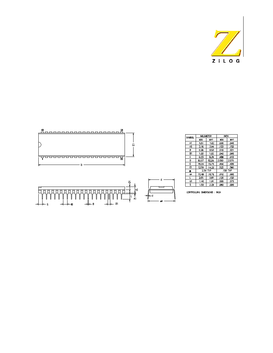
Z8 Encore!
�
64K Series
Product Specification
PS019915-1005
Packaging
257
Packaging
Figure 62 illustrates the 40-pin PDIP (plastic dual-inline package) available for the
Z8X1601, Z8X2401, Z8X3201, Z8X4801, and Z8X6401 devices.
Figure 62. 40-Lead Plastic Dual-Inline Package (PDIP)
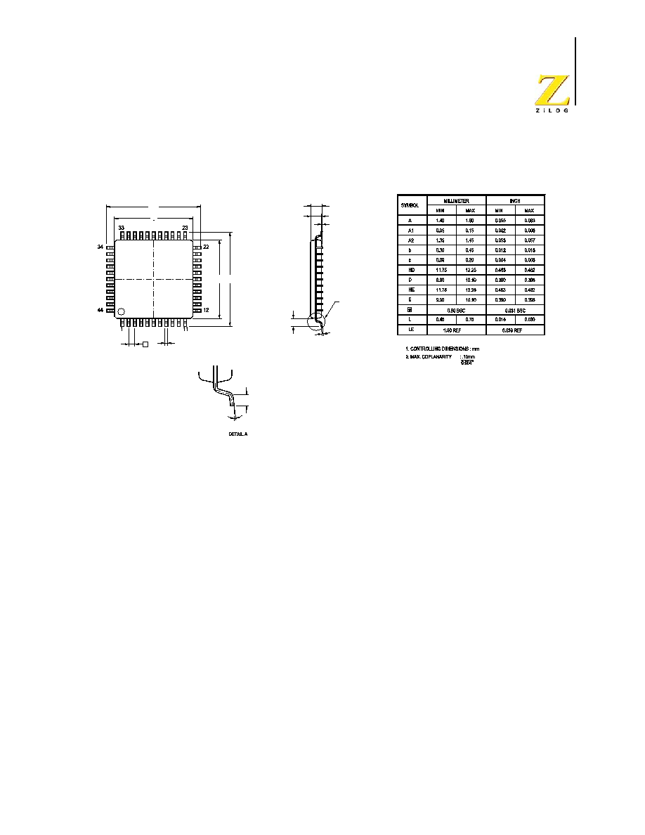
PS019915-1005
Packaging
Z8 Encore!
�
64K Series
Product Specification
258
Figure 63 illustrates the 44-pin LQFP (low profile quad flat package) available for the
Z8X1621, Z8X2421, Z8X3221, Z8X4821, and Z8X6421 devices.
Figure 63. 44-Lead Low-Profile Quad Flat Package (LQFP)
A2
A
A1
LE
c
E HE
e
L
0-7�
b
D
HD
DETAIL A
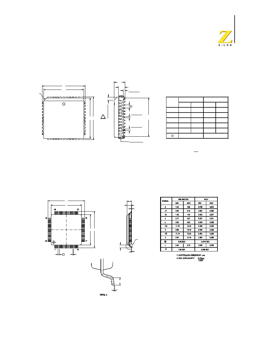
PS019915-1005
Packaging
Z8 Encore!
�
64K Series
Product Specification
259
Figure 64 illustrates the 44-pin PLCC (plastic lead chip carrier) package available for the
Z8X1621, Z8X2421, Z8X3221, Z8X4821, and Z8X6421 devices.
Figure 64. 44-Lead Plastic Lead Chip Carrier Package (PLCC)
Figure 64 illustrates the 64-pin LQFP (low-profile quad flat package) available for the
Z8X1622, Z8X2422, Z8X3222, Z8X4822, and Z8X6422 devices.
Figure 65. 64-Lead Low-Profile Quad Flat Package (LQFP)
0.020/0.014
0.045/0.025
0.032/0.026
R 1.14/0.64
.028/.020
0.51/0.36
0.81/0.66
D2
E
E1
3. DIMENSION : MM
2. LEADS ARE COPLANAR WITHIN 0.004".
1. CONTROLLING DIMENSION : INCH
NOTES:
17
18
INCH
29
28
D
D1
6
1
7
45�
40
39
A1
A
0.71/0.51
1.321/1.067
0.052/0.042
e
D
I
M. FRO
M
CENT
E
R
TO
CEN
T
E
R
O
F
RAD
I
I
D/E
0.650
0.600
D1/E1
e
D2
1.27 BSC
16.51
15.24
16.00
16.66
0.050 BSC
0.630
0.656
MIN
0.168
0.095
0.685
SYMBOL
A1
A
MILLIMETER
4.27
2.41
17.40
MIN
2.92
17.65
4.57
MAX
0.115
0.695
0.180
INCH
MAX
M
c
A1
A2
A
LE
E HE
e
0-7�
L
b
HD
D
DETAIL A
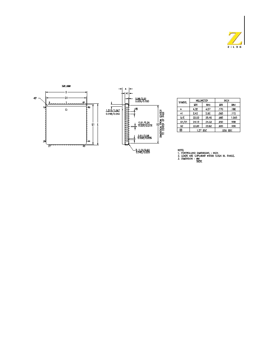
PS019915-1005
Packaging
Z8 Encore!
�
64K Series
Product Specification
260
Figure 66 illustrates the 68-pin PLCC (plastic lead chip carrier) package available for the
Z8X1622, Z8X2422, Z8X3222, Z8X4822, and Z8X6422 devices.
Figure 66. 68-Lead Plastic Lead Chip Carrier Package (PLCC)
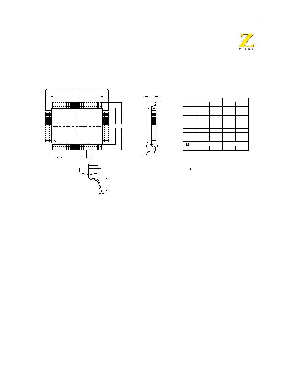
PS019915-1005
Packaging
Z8 Encore!
�
64K Series
Product Specification
261
Figure 67 illustrates the 80-pin QFP (quad flat package) available for the Z8X4823 and
Z8X6423 devices.
Figure 67. 80-Lead Quad-Flat Package (QFP)
A2
E
HE
1
80
b
DETAIL A
0-10�
L
e
24
25
DETAIL A
HD
D
65
64
40
41
17.70
HE
18.15
.715
.697
.004"
CONTROLLING DIMENSIONS : MILLIMETER
L
e
E
c
LEAD COPLANARITY : MAX .10
NOTES:
2.
0.80 BSC
0.70
13.90
1.10
14.10
.028
.043
.0315 BSC
.547
.555
A1
D
HD
c
b
A2
SYMBOL
A1
19.90
23.70
0.13
2.60
0.30
0.10
20.10
24.15
0.20
0.38
2.80
0.45
MILLIMETER
MIN
MAX
.783
.933
.005
.791
.951
.008
.102
.012
.004
.110
.018
.015
INCH
MIN
MAX
PS019915-1005
Ordering
Information
Z8 Encore!
�
64K Series
Product Specification
262
Ordering Information
P
a
rt Number
Flash
RA
M
I/
O Li
ne
s
In
ter
r
upt
s
16-Bit T
i
mers w/PWM
10-Bit A
/
D
Channels
I
2
C
SP
I
U
ART
s wi
th
IrDA
De
scr
ip
tion
Z8F642x with 64KB Flash, 10-Bit Analog-to-Digital Converter
Standard Temperature: 0� to 70�C
Z8F6421PM020SC
64KB
4KB
29 23 3
8
1
1
2 PDIP 40-pin package
Z8F6421AN020SC
64KB
4KB
31 23 3
8
1
1
2 LQFP 44-pin package
Z8F6421VN020SC
64KB
4KB
31 23 3
8
1
1
2 PLCC 44-pin package
Z8F6422AR020SC
64KB
4KB
46 24 4
12
1
1
2 LQFP 64-pin package
Z8F6422VS020SC
64KB
4KB
46 24 4
12
1
1
2 PLCC 68-pin package
Z8F6423FT020SC
64KB
4KB
60 24 4
12
1
1
2 QFP 80-pin package
Extended Temperature: �40� to +105�C
Z8F6421PM020EC
64KB
4KB
29 23 3
8
1
1
2 PDIP 40-pin package
Z8F6421AN020EC
64KB
4KB
31 23 3
8
1
1
2 LQFP 44-pin package
Z8F6421VN020EC
64KB
4KB
31 23 3
8
1
1
2 PLCC 44-pin package
Z8F6422AR020EC
64KB
4KB
46 24 4
12
1
1
2 LQFP 64-pin package
Z8F6422VS020EC
64KB
4KB
46 24 4
12
1
1
2 PLCC 68-pin package
Z8F6423FT020EC
64KB
4KB
60 24 4
12
1
1
2 QFP 80-pin package
Automotive/Industrial Temperature: �40� to +125�C
Z8F6421PM020AC
64KB
4KB
29 23 3
8
1
1
2 PDIP 40-pin package
Z8F6421AN020AC
64KB
4KB
31 23 3
8
1
1
2 LQFP 44-pin package
Z8F6421VN020AC
64KB
4KB
31 23 3
8
1
1
2 PLCC 44-pin package
Z8F6422AR020AC
64KB
4KB
46 24 4
12
1
1
2 LQFP 64-pin package
Z8F6422VS020AC
64KB
4KB
46 24 4
12
1
1
2 PLCC 68-pin package
Z8F6423FT020AC
64KB
4KB
60 24 4
12
1
1
2 QFP 80-pin package
Note: Replace C with G for lead-free packaging.
PS019915-1005
Ordering
Information
Z8 Encore!
�
64K Series
Product Specification
263
Z8F482x with 48KB Flash, 10-Bit Analog-to-Digital Converter
Standard Temperature: 0� to 70�C
Z8F4821PM020SC
48KB
4KB
29 23 3
8
1
1
2 PDIP 40-pin package
Z8F4821AN020SC
48KB
4KB
31 23 3
8
1
1
2 LQFP 44-pin package
Z8F4821VN020SC
48KB
4KB
31 23 3
8
1
1
2 PLCC 44-pin package
Z8F4822AR020SC
48KB
4KB
46 24 4
12
1
1
2 LQFP 64-pin package
Z8F4822VS020SC
48KB
4KB
46 24 4
12
1
1
2 PLCC 68-pin package
Z8F4823FT020SC
48KB
4KB
60 24 4
12
1
1
2 QFP 80-pin package
Extended Temperature: �40� to +105�C
Z8F4821PM020EC
48KB
4KB
29 23 3
8
1
1
2 PDIP 40-pin package
Z8F4821AN020EC
48KB
4KB
31 23 3
8
1
1
2 LQFP 44-pin package
Z8F4821VN020EC
48KB
4KB
31 23 3
8
1
1
2 PLCC 44-pin package
Z8F4822AR020EC
48KB
4KB
46 24 4
12
1
1
2 LQFP 64-pin package
Z8F4822VS020EC
48KB
4KB
46 24 4
12
1
1
2 PLCC 68-pin package
Z8F4823FT020EC
48KB
4KB
46 24 4
12
1
1
2 QFP 80-pin package
Automotive/Industrial Temperature: �40� to +125�C
Z8F4821PM020AC
48KB
4KB
29 23 3
8
1
1
2 PDIP 40-pin package
Z8F4821AN020AC
48KB
4KB
31 23 3
8
1
1
2 LQFP 44-pin package
Z8F4821VN020AC
48KB
4KB
31 23 3
8
1
1
2 PLCC 44-pin package
Z8F4822AR020AC
48KB
4KB
46 24 4
12
1
1
2 LQFP 64-pin package
Z8F4822VS020AC
48KB
4KB
46 24 4
12
1
1
2 PLCC 68-pin package
Z8F4823FT020AC
48KB
4KB
46 24 4
12
1
1
2 QFP 80-pin package
P
a
rt Number
Fla
s
h
RA
M
I/
O Li
ne
s
Int
e
r
r
upt
s
16-Bit T
i
mers
w/PWM
10-Bit A/D Channels
I
2
C
SP
I
U
ART
s wi
th
IrDA
De
scr
ip
tion
Note: Replace C with G for lead-free packaging.

PS019915-1005
Ordering
Information
Z8 Encore!
�
64K Series
Product Specification
264
Z8F322x with 32KB Flash, 10-Bit Analog-to-Digital Converter
Standard Temperature: 0� to 70�C
Z8F3221PM020SC
32KB
2KB
29 23 3
8
1
1
2 PDIP 40-pin package
Z8F3221AN020SC
32KB
2KB
31 23 3
8
1
1
2 LQFP 44-pin package
Z8F3221VN020SC
32KB
2KB
31 23 3
8
1
1
2 PLCC 44-pin package
Z8F3222AR020SC
32KB
2KB
46 24 4
12
1
1
2 LQFP 64-pin package
Z8F3222VS020SC
32KB
2KB
46 24 4
12
1
1
2 PLCC 68-pin package
Extended Temperature: �40� to 105�C
Z8F3221PM020EC
32KB
2KB
29 23 3
8
1
1
2 PDIP 40-pin package
Z8F3221AN020EC
32KB
2KB
31 23 3
8
1
1
2 LQFP 44-pin package
Z8F3221VN020EC
32KB
2KB
31 23 3
8
1
1
2 PLCC 44-pin package
Z8F3222AR020EC
32KB
2KB
46 24 4
12
1
1
2 LQFP 64-pin package
Z8F3222VS020EC
32KB
2KB
46 24 4
12
1
1
2 PLCC 68-pin package
Automotive/Industrial Temperature: �40� to 125�C
Z8F3221PM020AC
32KB
2KB
29 23 3
8
1
1
2 PDIP 40-pin package
Z8F3221AN020AC
32KB
2KB
31 23 3
8
1
1
2 LQFP 44-pin package
Z8F3221VN020AC
32KB
2KB
31 23 3
8
1
1
2 PLCC 44-pin package
Z8F3222AR020AC
32KB
2KB
46 24 4
12
1
1
2 LQFP 64-pin package
Z8F3222VS020AC
32KB
2KB
46 24 4
12
1
1
2 PLCC 68-pin package
P
a
rt Number
Fla
s
h
RA
M
I/
O Li
ne
s
Int
e
r
r
upt
s
16-Bit T
i
mers
w/PWM
10-Bit A/D Channels
I
2
C
SP
I
U
ART
s wi
th
IrDA
De
scr
ip
tion
Note: Replace C with G for lead-free packaging.
PS019915-1005
Ordering
Information
Z8 Encore!
�
64K Series
Product Specification
265
Z8F242x with 24KB Flash, 10-Bit Analog-to-Digital Converter
Standard Temperature: 0� to 70�C
Z8F2421PM020SC
24KB
2KB
29 23 3
8
1
1
2 PDIP 40-pin package
Z8F2421AN020SC
24KB
2KB
31 23 3
8
1
1
2 LQFP 44-pin package
Z8F2421VN020SC
24KB
2KB
31 23 3
8
1
1
2 PLCC 44-pin package
Z8F2422AR020SC
24KB
2KB
46 24 4
12
1
1
2 LQFP 64-pin package
Z8F2422VS020SC
24KB
2KB
46 24 4
12
1
1
2 PLCC 68-pin package
Extended Temperature: �40� to 105�C
Z8F2421PM020EC
24KB
2KB
29 23 3
8
1
1
2 PDIP 40-pin package
Z8F2421AN020EC
24KB
2KB
31 23 3
8
1
1
2 LQFP 44-pin package
Z8F2421VN020EC
24KB
2KB
31 23 3
8
1
1
2 PLCC 44-pin package
Z8F2422AR020EC
24KB
2KB
46 24 4
12
1
1
2 LQFP 64-pin package
Z8F2422VS020EC
24KB
2KB
46 24 4
12
1
1
2 PLCC 68-pin package
Automotive/Industrial Temperature: �40� to 125�C
Z8F2421PM020AC
24KB
2KB
29 23 3
8
1
1
2 PDIP 40-pin package
Z8F2421AN020AC
24KB
2KB
31 23 3
8
1
1
2 LQFP 44-pin package
Z8F2421VN020AC
24KB
2KB
31 23 3
8
1
1
2 PLCC 44-pin package
Z8F2422AR020AC
24KB
2KB
46 24 4
12
1
1
2 LQFP 64-pin package
Z8F2422VS020AC
24KB
2KB
46 24 4
12
1
1
2 PLCC 68-pin package
P
a
rt Number
Fla
s
h
RA
M
I/
O Li
ne
s
Int
e
r
r
upt
s
16-Bit T
i
mers
w/PWM
10-Bit A/D Channels
I
2
C
SP
I
U
ART
s wi
th
IrDA
De
scr
ip
tion
Note: Replace C with G for lead-free packaging.
PS019915-1005
Ordering
Information
Z8 Encore!
�
64K Series
Product Specification
266
For technical and customer support, hardware and software development tools, visit the
ZiLOG web site at
www.zilog.com
. The latest released version of ZDS can be down-
loaded from this site.
Z8F162x with 16KB Flash, 10-Bit Analog-to-Digital Converter
Standard Temperature: 0� to 70�C
Z8F1621PM020SC
16KB
2KB
29 23 3
8
1
1
2 PDIP 40-pin package
Z8F1621AN020SC
16KB
2KB
31 23 3
8
1
1
2 LQFP 44-pin package
Z8F1621VN020SC
16KB
2KB
31 23 3
8
1
1
2 PLCC 44-pin package
Z8F1622AR020SC
16KB
2KB
46 24 4
12
1
1
2 LQFP 64-pin package
Z8F1622VS020SC
16KB
2KB
46 24 4
12
1
1
2 PLCC 68-pin package
Extended Temperature: �40� to +105�C
Z8F1621PM020EC
16KB
2KB
29 23 3
8
1
1
2 PDIP 40-pin package
Z8F1621AN020EC
16KB
2KB
31 23 3
8
1
1
2 LQFP 44-pin package
Z8F1621VN020EC
16KB
2KB
31 23 3
8
1
1
2 PLCC 44-pin package
Z8F1622AR020EC
16KB
2KB
46 24 4
12
1
1
2 LQFP 64-pin package
Z8F1622VS020EC
16KB
2KB
46 24 4
12
1
1
2 PLCC 68-pin package
Automotive/Industrial Temperature: �40� to +125�C
Z8F1621PM020AC
16KB
2KB
29 23 3
8
1
1
2 PDIP 40-pin package
Z8F1621AN020AC
16KB
2KB
31 23 3
8
1
1
2 LQFP 44-pin package
Z8F1621VN020AC
16KB
2KB
31 23 3
8
1
1
2 PLCC 44-pin package
Z8F1622AR020AC
16KB
2KB
46 24 4
12
1
1
2 LQFP 64-pin package
Z8F1622VS020AC
16KB
2KB
46 24 4
12
1
1
2 PLCC 68-pin package
Z8F64200100KIT
Development Kit
P
a
rt Number
Fla
s
h
RA
M
I/
O Li
ne
s
Int
e
r
r
upt
s
16-Bit T
i
mers
w/PWM
10-Bit A/D Channels
I
2
C
SP
I
U
ART
s wi
th
IrDA
De
scr
ip
tion
Note: Replace C with G for lead-free packaging.

PS019915-1005
Ordering
Information
Z8 Encore!
�
64K Series
Product Specification
267
Part Number Suffix Designations
Example: Part number Z8F6421AN020SC is an 8-bit microcontroller product in an LQFP package,
using 44 pins, operating with a maximum 20MHz external clock frequency over a 0�C to +70�C
temperature range and built using the Plastic-Standard environmental flow.
Z8 F 64 21 A
N 020 S
C
Environmental Flow: C = Plastic Standard
G = Lead Free Package
Temperature Range (�C):
S = Standard, 0 to 70
E = Extended, �40 to +105
A = Automotive/Industrial, �40 to +125
Speed:
020 = 20MHz
Pin Count:
M = 40 pins
N = 44 pins
R = 64 pins
S = 68 pins
T = 80 pins
Package:
A = LQFP
F = QFP
P = PDIP
V = PLCC
Device Type
Memory Size:
64 KB Flash, 4 KB RAM
48 KB Flash, 4 KB RAM
32 KB Flash, 2 KB RAM
24 KB Flash, 2 KB RAM
16 KB Flash, 2 KB RAM
Memory Type:
F = Flash
Device Family

PS019915-1005
Ordering
Information
Z8 Encore!
�
64K Series
Product Specification
268
Document Information
Document Number Description
The Document Control Number that appears in the footer on each page of this document
contains unique identifying attributes, as indicated in the following table:
PS
Product Specification
0199
Unique Document Number
07
Revision Number
0204
Month and Year Published

PS019915-1005
Ordering
Information
Z8 Encore!
�
64K Series
Product Specification
269
Customer Feedback Form
The Z8 Encore!
�
64K Series Product Specification
If you experience any problems while operating this product, or if you note any inaccuracies while reading
this Product Specification, please copy and complete this form, then mail or fax it to ZiLOG (see Return
Information, below). We also welcome your suggestions!
Customer Information
Product Information
Return Information
ZiLOG, Inc.
532 Race Street
San Jose, CA 95126
Fax: (408) 558-8536
Problem Description or Suggestion
Provide a complete description of the problem or your suggestion. If you are reporting a specific problem,
include all steps leading up to the occurrence of the problem. Attach additional pages as necessary.
______________________________________________________________________________________
______________________________________________________________________________________
______________________________________________________________________________________
______________________________________________________________________________________
______________________________________________________________________________________
______________________________________________________________________________________
______________________________________________________________________________________
______________________________________________________________________________________
Name
Country
Company
Phone
Address
Fax
City/State/Zip
E-Mail
Part #, Serial #, Board Fab #, or Rev. #
Software Version
Document Number
Host Computer Description/Type

PS019915-1005
Index
Z8 Encore!
�
64K Series
Product Specification
270
Index
Symbols
#
236
%
236
@
236
Numerics
10-bit ADC
4
40-lead plastic dual-inline package
257
44-lead low-profile quad flat package
258
44-lead plastic lead chip carrier package
259
64-lead low-profile quad flat package
259
68-lead plastic lead chip carrier package
260
80-lead quad flat package
261
A
absolute maximum ratings
209
AC characteristics
224
ADC
238
architecture
171
automatic power-down
172
block diagram
172
continuous conversion
173
control register
175
control register definitions
175
data high byte register
176
data low bits register
176
DMA control
174
electrical characteristics and timing
222
operation
172
single-shot conversion
173
ADCCTL register
175
ADCDH register
176
ADCDL register
176
ADCX
238
ADD
238
add - extended addressing
238
add with carry
238
add with carry - extended addressing
238
additional symbols
236
address space
17
ADDX
238
analog signals
14
analog-to-digital converter (ADC)
171
AND
241
ANDX
241
arithmetic instructions
238
assembly language programming
233
assembly language syntax
234
B
B
236
b
235
baud rate generator, UART
108
BCLR
239
binary number suffix
236
BIT
239
bit
235
clear
239
manipulation instructions
239
set
239
set or clear
239
swap
239
test and jump
241
test and jump if non-zero
241
test and jump if zero
241
bit jump and test if non-zero
241
bit swap
242
block diagram
3
block transfer instructions
239
BRK
241
BSET
239
BSWAP
239
,
242
BTJ
241
BTJNZ
241
BTJZ
241
C
CALL procedure
241
capture mode
89
capture/compare mode
89

PS019915-1005
Index
Z8 Encore!
�
64K Series
Product Specification
271
cc
235
CCF
240
characteristics, electrical
209
clear
240
clock phase (SPI)
128
CLR
240
COM
241
compare
89
compare - extended addressing
238
compare mode
89
compare with carry
238
compare with carry - extended addressing
238
complement
241
complement carry flag
239
,
240
condition code
235
continuous conversion (ADC)
173
continuous mode
89
control register definition, UART
109
control register, I2C
155
counter modes
89
CP
238
CPC
238
CPCX
238
CPU and peripheral overview
3
CPU control instructions
240
CPX
238
customer feedback form
269
customer information
269
D
DA
235
,
238
data register, I2C
152
DC characteristics
211
debugger, on-chip
193
DEC
238
decimal adjust
238
decrement
238
decrement and jump non-zero
241
decrement word
238
DECW
238
destination operand
236
device, port availability
51
DI
240
direct address
235
direct memory access controller
161
disable interrupts
240
DJNZ
241
DMA
address high nibble register
165
configuring for DMA_ADC data transfer
163
confiigurting DMA0-1 data transfer
162
control of ADC
174
control register
163
control register definitions
163
controller
5
DMA_ADC address register
167
DMA_ADC control register
168
DMA_ADC operation
162
end address low byte register
166
I/O address register
165
operation
161
start/current address low byte register
166
status register
169
DMAA_STAT register
169
DMAACTL register
168
DMAxCTL register
164
DMAxEND register
167
DMAxH register
165
DMAxI/O address (DMAxIO)
165
DMAxIO register
165
DMAxSTART register
166
document number description
268
dst
236
E
EI
240
electrical characteristics
209
ADC
222
flash memory and timing
221
GPIO input data sample timing
225
watch-dog timer
221
enable interrupt
240
ER
235
extended addressing register
235
external pin reset
46
external RC oscillator
220

PS019915-1005
Index
Z8 Encore!
�
64K Series
Product Specification
272
eZ8 CPU features
3
eZ8 CPU instruction classes
238
eZ8 CPU instruction notation
234
eZ8 CPU instruction set
233
eZ8 CPU instruction summary
242
F
FCTL register
185
features, Z8 Encore!
1
first opcode map
255
FLAGS
236
flags register
236
flash
controller
4
option bit address space
190
option bit configuration - reset
190
program memory address 0001H
192
flash memory
arrangement
179
byte programming
182
code protection
181
configurations
178
control register definitions
185
controller bypass
184
electrical characteristics and timing
221
flash control register
185
flash status register
186
frequency high and low byte registers
189
mass erase
184
operation
180
operation timing
181
page erase
183
page select register
187
FPS register
187
FSTAT register
186
G
gated mode
89
general-purpose I/O
51
GPIO
4
,
51
alternate functions
52
architecture
52
control register definitions
54
input data sample timing
225
interrupts
54
port A-H address registers
55
port A-H alternate function sub-registers
57
port A-H control registers
56
port A-H data direction sub-registers
57
port A-H high drive enable sub-registers
59
port A-H input data registers
60
port A-H output control sub-registers
58
port A-H output data registers
61
port A-H STOP mode recovery sub-registers
59
port availability by device
51
port input timing
225
port output timing
226
H
H
236
HALT
240
halt mode
50
,
240
hexadecimal number prefix/suffix
236
I
I2C
4
10-bit address read transaction
150
10-bit address transaction
147
10-bit addressed slave data transfer format
147
10-bit receive data format
150
7-bit address transaction
145
7-bit address, reading a transaction
149
7-bit addressed slave data transfer format
144
,
145
,
146
7-bit receive data transfer format
149
baud high and low byte registers
156
,
158
,
160
C status register
153
control register definitions
152
controller
139
controller signals
13
interrupts
141
operation
140
SDA and SCL signals
141
stop and start conditions
143

PS019915-1005
Index
Z8 Encore!
�
64K Series
Product Specification
273
I2CBRH register
157
,
158
,
160
I2CBRL register
157
I2CCTL register
155
I2CDATA register
153
I2CSTAT register
153
IM
235
immediate data
235
immediate operand prefix
236
INC
238
increment
238
increment word
238
INCW
238
indexed
235
indirect address prefix
236
indirect register
235
indirect register pair
235
indirect working register
235
indirect working register pair
235
infrared encoder/decoder (IrDA)
120
instruction set, ez8 CPU
233
instructions
ADC
238
ADCX
238
ADD
238
ADDX
238
AND
241
ANDX
241
arithmetic
238
BCLR
239
BIT
239
bit manipulation
239
block transfer
239
BRK
241
BSET
239
BSWAP
239
,
242
BTJ
241
BTJNZ
241
BTJZ
241
CALL
241
CCF
239
,
240
CLR
240
COM
241
CP
238
CPC
238
CPCX
238
CPU control
240
CPX
238
DA
238
DEC
238
DECW
238
DI
240
DJNZ
241
EI
240
HALT
240
INC
238
INCW
238
IRET
241
JP
241
LD
240
LDC
240
LDCI
239
,
240
LDE
240
LDEI
239
LDX
240
LEA
240
load
240
logical
241
MULT
238
NOP
240
OR
241
ORX
241
POP
240
POPX
240
program control
241
PUSH
240
PUSHX
240
RCF
239
,
240
RET
241
RL
242
RLC
242
rotate and shift
242
RR
242
RRC
242
SBC
239
SCF
239
,
240
SRA
242
SRL
242
SRP
240

PS019915-1005
Index
Z8 Encore!
�
64K Series
Product Specification
274
STOP
240
SUB
239
SUBX
239
SWAP
242
TCM
239
TCMX
239
TM
239
TMX
239
TRAP
241
watch-dog timer refresh
240
XOR
241
XORX
241
instructions, eZ8 classes of
238
interrupt control register
74
interrupt controller
5
,
62
architecture
62
interrupt assertion types
65
interrupt vectors and priority
65
operation
64
register definitions
66
software interrupt assertion
65
interrupt edge select register
72
interrupt port select register
73
interrupt request 0 register
66
interrupt request 1 register
67
interrupt request 2 register
68
interrupt return
241
interrupt vector listing
62
interrupts
not acknowledge
141
receive
141
SPI
131
transmit
141
UART
106
introduction
1
IR
235
Ir
235
IrDA
architecture
120
block diagram
120
control register definitions
124
operation
121
receiving data
122
transmitting data
121
IRET
241
IRQ0 enable high and low bit registers
69
IRQ1 enable high and low bit registers
70
IRQ2 enable high and low bit registers
71
IRR
235
Irr
235
J
JP
241
jump, conditional, relative, and relative conditional
241
L
LD
240
LDC
240
LDCI
239
,
240
LDE
240
LDEI
239
,
240
LDX
240
LEA
240
load
240
load constant
239
load constant to/from program memory
240
load constant with auto-increment addresses
240
load effective address
240
load external data
240
load external data to/from data memory and auto-
increment addresses
239
load external to/from data memory and auto-incre-
ment addresses
240
load instructions
240
load using extended addressing
240
logical AND
241
logical AND/extended addressing
241
logical exclusive OR
241
logical exclusive OR/extended addressing
241
logical instructions
241
logical OR
241
logical OR/extended addressing
241
low power modes
49
LQFP
44 lead
258

PS019915-1005
Index
Z8 Encore!
�
64K Series
Product Specification
275
64 lead
259
M
master interrupt enable
64
master-in, slave-out and-in
127
memory
program
18
MISO
127
mode
capture
89
capture/compare
89
continuous
89
counter
89
gated
89
one-shot
89
PWM
89
modes
89
MOSI
127
MULT
238
multiply
238
multiprocessor mode, UART
104
N
NOP (no operation)
240
not acknowledge interrupt
141
notation
b
235
cc
235
DA
235
ER
235
IM
235
IR
235
Ir
235
IRR
235
Irr
235
p
235
R
235
r
235
RA
235
RR
235
rr
235
vector
235
X
235
notational shorthand
235
O
OCD
architecture
193
auto-baud detector/generator
196
baud rate limits
196
block diagram
193
breakpoints
197
commands
198
control register
202
data format
196
DBG pin to RS-232 Interface
194
debug mode
195
debugger break
241
interface
194
serial errors
197
status register
204
timing
227
OCD commands
execute instruction (12H)
202
read data memory (0DH)
201
read OCD control register (05H)
200
read OCD revision (00H)
199
read OCD status register (02H)
199
read program counter (07H)
200
read program memory (0BH)
201
read program memory CRC (0EH)
201
read register (09H)
200
step instruction (10H)
202
stuff instruction (11H)
202
write data memory (0CH)
201
write OCD control register (04H)
199
write program counter (06H)
200
write program memory (0AH)
200
write register (08H)
200
on-chip debugger
5
on-chip debugger (OCD)
193
on-chip debugger signals
15
on-chip oscillator
205
one-shot mode
89
opcode map

PS019915-1005
Index
Z8 Encore!
�
64K Series
Product Specification
276
abbreviations
254
cell description
253
first
255
second after 1FH
256
Operational Description
98
OR
241
ordering information
262
ORX
241
oscillator signals
14
P
p
235
packaging
LQFP
44 lead
258
64 lead
259
PDIP
257
PLCC
44 lead
259
68 lead
260
QFP
261
part number description
267
part selection guide
2
PC
236
PDIP
257
peripheral AC and DC electrical characteristics
219
PHASE=0 timing (SPI)
129
PHASE=1 timing (SPI)
130
pin characteristics
16
PLCC
44 lead
259
68-lead
260
polarity
235
POP
240
pop using extended addressing
240
POPX
240
port availability, device
51
port input timing (GPIO)
225
port output timing, GPIO
226
power supply signals
15
power-down, automatic (ADC)
172
power-on and voltage brown-out
219
power-on reset (POR)
44
problem description or suggestion
269
product information
269
program control instructions
241
program counter
236
program memory
18
PUSH
240
push using extended addressing
240
PUSHX
240
PWM mode
89
PxADDR register
55
PxCTL register
56
Q
QFP
261
R
R
235
r
235
RA
register address
235
RCF
239
,
240
receive
10-bit data format (I2C)
150
7-bit data transfer format (I2C)
149
IrDA data
122
receive interrupt
141
receiving UART data-interrupt-driven method
103
receiving UART data-polled method
102
register
136
,
165
,
235
ADC control (ADCCTL)
175
ADC data high byte (ADCDH)
176
ADC data low bits (ADCDL)
176
baud low and high byte (I2C)
156
,
158
,
160
baud rate high and low byte (SPI)
138
control (SPI)
133
control, I2C
155
data, SPI
133
DMA status (DMAA_STAT)
169
DMA_ADC address
167
DMA_ADC control DMAACTL)
168
DMAx address high nibble (DMAxH)
165
DMAx control (DMAxCTL)
164

PS019915-1005
Index
Z8 Encore!
�
64K Series
Product Specification
277
DMAx end/address low byte (DMAxEND)
167
DMAx start/current address low byte register
(DMAxSTART)
166
flash control (FCTL)
185
flash high and low byte (FFREQH and FRE-
EQL)
189
flash page select (FPS)
187
flash status (FSTAT)
186
GPIO port A-H address (PxADDR)
55
GPIO port A-H alternate function sub-registers
57
GPIO port A-H control address (PxCTL)
56
GPIO port A-H data direction sub-registers
57
I2C baud rate high (I2CBRH)
157
,
158
,
160
I2C control (I2CCTL)
155
I2C data (I2CDATA)
153
I2C status
153
I2C status (I2CSTAT)
153
I2Cbaud rate low (I2CBRL)
157
mode, SPI
136
OCD control
202
OCD status
204
SPI baud rate high byte (SPIBRH)
138
SPI baud rate low byte (SPIBRL)
138
SPI control (SPICTL)
134
SPI data (SPIDATA)
133
SPI status (SPISTAT)
135
status, I2C
153
status, SPI
135
UARTx baud rate high byte (UxBRH)
116
UARTx baud rate low byte (UxBRL)
116
UARTx Control 0 (UxCTL0)
112
,
115
UARTx control 1 (UxCTL1)
113
UARTx receive data (UxRXD)
110
UARTx status 0 (UxSTAT0)
110
UARTx status 1 (UxSTAT1)
112
UARTx transmit data (UxTXD)
109
watch-dog timer control (WDTCTL)
94
watch-dog timer reload high byte (WDTH)
96
watch-dog timer reload low byte (WDTL)
97
watch-dog timer reload upper byte (WDTU)
96
register file
17
register file address map
21
register pair
235
register pointer
236
reset
and STOP mode characteristics
43
and STOP mode recovery
43
carry flag
239
controller
5
sources
44
RET
241
return
241
return information
269
RL
242
RLC
242
rotate and shift instructions
242
rotate left
242
rotate left through carry
242
rotate right
242
rotate right through carry
242
RP
236
RR
235
,
242
rr
235
RRC
242
S
SBC
239
SCF
239
,
240
SCK
127
SDA and SCL (IrDA) signals
141
second opcode map after 1FH
256
serial clock
127
serial peripheral interface (SPI)
125
set carry flag
239
,
240
set register pointer
240
shift right arithmetic
242
shift right logical
242
signal descriptions
13
single-shot conversion (ADC)
173
SIO
5
slave data transfer formats (I2C)
147
slave select
128
software trap
241
source operand
236
SP
236
SPI

PS019915-1005
Index
Z8 Encore!
�
64K Series
Product Specification
278
architecture
125
baud rate generator
132
baud rate high and low byte register
138
clock phase
128
configured as slave
126
control register
133
control register definitions
133
data register
133
error detection
131
interrupts
131
mode fault error
131
mode register
136
multi-master operation
130
operation
126
overrun error
131
signals
127
single master, multiple slave system
126
single master, single slave system
125
status register
135
timing, PHASE = 0
129
timing, PHASE=1
130
SPI controller signals
13
SPI mode (SPIMODE)
136
SPIBRH register
138
SPIBRL register
138
SPICTL register
134
SPIDATA register
133
SPIMODE register
136
SPISTAT register
135
SRA
242
src
236
SRL
242
SRP
240
SS, SPI signal
127
stack pointer
236
status register, I2C
153
STOP
240
STOP mode
49
,
240
STOP mode recovery
sources
47
using a GPIO port pin transition
48
using watch-dog timer time-out
48
SUB
239
subtract
239
subtract - extended addressing
239
subtract with carry
239
subtract with carry - extended addressing
239
SUBX
239
SWAP
242
swap nibbles
242
symbols, additional
236
system and core resets
44
T
TCM
239
TCMX
239
test complement under mask
239
test complement under mask - extended addressing
239
test under mask
239
test under mask - extended addressing
239
timer signals
14
timers
5
,
75
architecture
75
block diagram
76
capture mode
80
,
89
capture/compare mode
83
,
89
compare mode
81
,
89
continuous mode
77
,
89
counter mode
78
counter modes
89
gated mode
82
,
89
one-shot mode
76
,
89
operating mode
76
PWM mode
79
,
89
reading the timer count values
84
reload high and low byte registers
85
timer control register definitions
84
timer output signal operation
84
timers 0-3
control 0 registers
88
control 1 registers
88
high and low byte registers
84
,
87
TM
239
TMX
239
transmit
IrDA data
121

PS019915-1005
Index
Z8 Encore!
�
64K Series
Product Specification
279
transmit interrupt
141
transmitting UART data-interrupt-driven method
101
transmitting UART data-polled method
100
TRAP
241
U
UART
4
architecture
98
asynchronous data format without/with parity
100
baud rate generator
108
baud rates table
117
control register definitions
109
controller signals
14
data format
99
interrupts
106
multiprocessor mode
104
receiving data using interrupt-driven method
103
receiving data using the polled method
102
transmitting data using the interrupt-driven
method
101
transmitting data using the polled method
100
x baud rate high and low registers
115
x control 0 and control 1 registers
112
x status 0 and status 1 registers
110
,
112
UxBRH register
116
UxBRL register
116
UxCTL0 register
112
,
115
UxCTL1 register
113
UxRXD register
110
UxSTAT0 register
110
UxSTAT1 register
112
UxTXD register
109
V
vector
235
voltage brown-out reset (VBR)
45
W
watch-dog timer
approximate time-out delay
92
approximate time-out delays
91
CNTL
46
control register
94
electrical characteristics and timing
221
interrupt in normal operation
92
interrupt in STOP mode
92
operation
91
refresh
92
,
240
reload unlock sequence
93
reload upper, high and low registers
95
reset
46
reset in normal operation
93
reset in STOP mode
93
time-out response
92
WDTCTL register
94
WDTH register
96
WDTL register
97
working register
235
working register pair
235
WTDU register
96
X
X
235
XOR
241
XORX
241
Z
Z8 Encore!
block diagram
3
features
1
introduction
1
part selection guide
2