
ZiLOG Worldwide Headquarters � 532 Race Street � San Jose, CA 95126-3432
Telephone: 408.558.8500 � Fax: 408.558.8300 �
www.ZiLOG.com
PS024604-1005
P R E L I M I N A R Y
Product Specification
Z8 Encore!
�
Motor Control Flash MCUs
Z8FMC16100 Series

PS024604-1005
P R E L I M I N A R Y
This publication is subject to replacement by a later edition. To determine whether a later edition exists, or
to request copies of publications, contact:
ZiLOG Worldwide Headquarters
532 Race Street
San Jose, CA 95126
Telephone: 408.558.8500
Fax: 408.558.8300
www.zilog.com
Document Disclaimer
ZiLOG is a registered trademark of ZiLOG Inc. in the United States and in other countries. All other products and/or service
names mentioned herein may be trademarks of the companies with which they are associated.
�2005 by ZiLOG, Inc. All rights reserved. Information in this publication concerning the devices, applications, or technology
described is intended to suggest possible uses and may be superseded. ZiLOG, INC. DOES NOT ASSUME LIABILITY FOR OR
PROVIDE A REPRESENTATION OF ACCURACY OF THE INFORMATION, DEVICES, OR TECHNOLOGY DESCRIBED
IN THIS DOCUMENT. ZiLOG ALSO DOES NOT ASSUME LIABILITY FOR INTELLECTUAL PROPERTY
INFRINGEMENT RELATED IN ANY MANNER TO USE OF INFORMATION, DEVICES, OR TECHNOLOGY DESCRIBED
HEREIN OR OTHERWISE. Devices sold by ZiLOG, Inc. are covered by warranty and limitation of liability provisions appearing
in the ZiLOG, Inc. Terms and Conditions of Sale. ZiLOG, Inc. makes no warranty of merchantability or fitness for any purpose
Except with the express written approval of ZiLOG, use of information, devices, or technology as critical components of life
support systems is not authorized. No licenses are conveyed, implicitly or otherwise, by this document under any intellectual
property rights.

PS024604-1005
P R E L I M I N A R Y
Table of Contents
Z8FMC16100 Series Flash MCU
Product Specification
iii
Table of Contents
Introduction . . . . . . . . . . . . . . . . . . . . . . . . . . . . . . . . . . . . . . . . . . . . . . . . . . . . . . . . . . . . 1
Z8FMC16100 Series Flash MCU Features . . . . . . . . . . . . . . . . . . . . . . . . . . . . . . . . . . . . 1
Block Diagram . . . . . . . . . . . . . . . . . . . . . . . . . . . . . . . . . . . . . . . . . . . . . . . . . . . . . . . . . . 2
CPU and Peripheral Overview . . . . . . . . . . . . . . . . . . . . . . . . . . . . . . . . . . . . . . . . . . . . . 3
Pulse-Width Modulator for Motor Control Applications . . . . . . . . . . . . . . . . . . . . . . 3
10-Bit Analog-to-Digital Converter . . . . . . . . . . . . . . . . . . . . . . . . . . . . . . . . . . . . . . 3
Analog Comparator . . . . . . . . . . . . . . . . . . . . . . . . . . . . . . . . . . . . . . . . . . . . . . . . . . . 4
Operational Amplifier . . . . . . . . . . . . . . . . . . . . . . . . . . . . . . . . . . . . . . . . . . . . . . . . . 4
General Purpose I/O . . . . . . . . . . . . . . . . . . . . . . . . . . . . . . . . . . . . . . . . . . . . . . . . . . 4
Flash Controller . . . . . . . . . . . . . . . . . . . . . . . . . . . . . . . . . . . . . . . . . . . . . . . . . . . . . 4
Random Access Memory (RAM) . . . . . . . . . . . . . . . . . . . . . . . . . . . . . . . . . . . . . . . . 4
UART with LIN and IrDA . . . . . . . . . . . . . . . . . . . . . . . . . . . . . . . . . . . . . . . . . . . . . 4
Serial Peripheral Interface . . . . . . . . . . . . . . . . . . . . . . . . . . . . . . . . . . . . . . . . . . . . . . 4
I
2
C . . . . . . . . . . . . . . . . . . . . . . . . . . . . . . . . . . . . . . . . . . . . . . . . . . . . . . . . . . . . . . . . 5
Internal Precision Oscillator . . . . . . . . . . . . . . . . . . . . . . . . . . . . . . . . . . . . . . . . . . . . 5
Crystal Oscillator . . . . . . . . . . . . . . . . . . . . . . . . . . . . . . . . . . . . . . . . . . . . . . . . . . . . 5
Standard Timer . . . . . . . . . . . . . . . . . . . . . . . . . . . . . . . . . . . . . . . . . . . . . . . . . . . . . . 5
Interrupt Controller . . . . . . . . . . . . . . . . . . . . . . . . . . . . . . . . . . . . . . . . . . . . . . . . . . . 5
Reset Controller . . . . . . . . . . . . . . . . . . . . . . . . . . . . . . . . . . . . . . . . . . . . . . . . . . . . . 5
On-Chip Debugger . . . . . . . . . . . . . . . . . . . . . . . . . . . . . . . . . . . . . . . . . . . . . . . . . . . 5
Signal and Pin Descriptions . . . . . . . . . . . . . . . . . . . . . . . . . . . . . . . . . . . . . . . . . . . . . . . . 7
Pin Configurations . . . . . . . . . . . . . . . . . . . . . . . . . . . . . . . . . . . . . . . . . . . . . . . . . . . . . . . 8
Signal Descriptions . . . . . . . . . . . . . . . . . . . . . . . . . . . . . . . . . . . . . . . . . . . . . . . . . . . . . . 9
Pin Characteristics . . . . . . . . . . . . . . . . . . . . . . . . . . . . . . . . . . . . . . . . . . . . . . . . . . . . . . 11
Address Space . . . . . . . . . . . . . . . . . . . . . . . . . . . . . . . . . . . . . . . . . . . . . . . . . . . . . . . . . 13
Register File . . . . . . . . . . . . . . . . . . . . . . . . . . . . . . . . . . . . . . . . . . . . . . . . . . . . . . . . . . . 13
Program Memory . . . . . . . . . . . . . . . . . . . . . . . . . . . . . . . . . . . . . . . . . . . . . . . . . . . . . . . 14
Data Memory . . . . . . . . . . . . . . . . . . . . . . . . . . . . . . . . . . . . . . . . . . . . . . . . . . . . . . . . . . 14
Information Area . . . . . . . . . . . . . . . . . . . . . . . . . . . . . . . . . . . . . . . . . . . . . . . . . . . . . . . 14
Register File Address Map . . . . . . . . . . . . . . . . . . . . . . . . . . . . . . . . . . . . . . . . . . . . . . . 17
Reset and Stop-Mode Recovery . . . . . . . . . . . . . . . . . . . . . . . . . . . . . . . . . . . . . . . . . . . 23
Reset Types . . . . . . . . . . . . . . . . . . . . . . . . . . . . . . . . . . . . . . . . . . . . . . . . . . . . . . . . . . . 23
System Reset . . . . . . . . . . . . . . . . . . . . . . . . . . . . . . . . . . . . . . . . . . . . . . . . . . . . . . . . . . 24
Power-On Reset . . . . . . . . . . . . . . . . . . . . . . . . . . . . . . . . . . . . . . . . . . . . . . . . . . . . 25

PS024604-1005
P R E L I M I N A R Y
Table of Contents
Z8FMC16100 Series Flash MCU
Product Specification
iv
Voltage Brown-Out Reset . . . . . . . . . . . . . . . . . . . . . . . . . . . . . . . . . . . . . . . . . . . . . 25
Watch-Dog Timer Reset . . . . . . . . . . . . . . . . . . . . . . . . . . . . . . . . . . . . . . . . . . . . . . 26
External Pin Reset . . . . . . . . . . . . . . . . . . . . . . . . . . . . . . . . . . . . . . . . . . . . . . . . . . . 27
External Reset Indicator . . . . . . . . . . . . . . . . . . . . . . . . . . . . . . . . . . . . . . . . . . . . . . 27
On-Chip Debugger Initiated Reset . . . . . . . . . . . . . . . . . . . . . . . . . . . . . . . . . . . . . . 27
Fault Detect Logic Reset . . . . . . . . . . . . . . . . . . . . . . . . . . . . . . . . . . . . . . . . . . . . . . 27
Stop-Mode Recovery . . . . . . . . . . . . . . . . . . . . . . . . . . . . . . . . . . . . . . . . . . . . . . . . . . . . 28
Stop-Mode Recovery Using Watch-Dog Timer Time-Out . . . . . . . . . . . . . . . . . . . 28
Stop-Mode Recovery Using a GPIO Port Pin Transition . . . . . . . . . . . . . . . . . . . . . 28
PWM Fault0 and Reset pin selection . . . . . . . . . . . . . . . . . . . . . . . . . . . . . . . . . . . . 29
Reset Control Register Definitions . . . . . . . . . . . . . . . . . . . . . . . . . . . . . . . . . . . . . . . . . 29
Reset Status and Control Register . . . . . . . . . . . . . . . . . . . . . . . . . . . . . . . . . . . . . . . 29
Low-Power Modes . . . . . . . . . . . . . . . . . . . . . . . . . . . . . . . . . . . . . . . . . . . . . . . . . . . . . 31
Stop Mode . . . . . . . . . . . . . . . . . . . . . . . . . . . . . . . . . . . . . . . . . . . . . . . . . . . . . . . . . . . . 31
Halt Mode . . . . . . . . . . . . . . . . . . . . . . . . . . . . . . . . . . . . . . . . . . . . . . . . . . . . . . . . . . . . 31
Peripheral-Level Power Control . . . . . . . . . . . . . . . . . . . . . . . . . . . . . . . . . . . . . . . . . . . 32
Power Control Register 0 . . . . . . . . . . . . . . . . . . . . . . . . . . . . . . . . . . . . . . . . . . . . . 33
General-Purpose I/O . . . . . . . . . . . . . . . . . . . . . . . . . . . . . . . . . . . . . . . . . . . . . . . . . . . . 35
GPIO Port Availability By Device . . . . . . . . . . . . . . . . . . . . . . . . . . . . . . . . . . . . . . . . . 35
Architecture . . . . . . . . . . . . . . . . . . . . . . . . . . . . . . . . . . . . . . . . . . . . . . . . . . . . . . . . . . . 35
GPIO Alternate Functions . . . . . . . . . . . . . . . . . . . . . . . . . . . . . . . . . . . . . . . . . . . . . . . . 36
GPIO Interrupts . . . . . . . . . . . . . . . . . . . . . . . . . . . . . . . . . . . . . . . . . . . . . . . . . . . . . . . . 39
GPIO Control Register Definitions . . . . . . . . . . . . . . . . . . . . . . . . . . . . . . . . . . . . . . . . . 39
Port A-C Address Registers . . . . . . . . . . . . . . . . . . . . . . . . . . . . . . . . . . . . . . . . . . . 40
Port A�C Control Registers . . . . . . . . . . . . . . . . . . . . . . . . . . . . . . . . . . . . . . . . . . . 41
Port A-C Input Data Registers . . . . . . . . . . . . . . . . . . . . . . . . . . . . . . . . . . . . . . . . . 48
Port A�C Output Data Registers . . . . . . . . . . . . . . . . . . . . . . . . . . . . . . . . . . . . . . . . 49
Interrupt Controller . . . . . . . . . . . . . . . . . . . . . . . . . . . . . . . . . . . . . . . . . . . . . . . . . . . . . 51
Interrupt and System Exception Vector Listing . . . . . . . . . . . . . . . . . . . . . . . . . . . . . . . 51
Architecture . . . . . . . . . . . . . . . . . . . . . . . . . . . . . . . . . . . . . . . . . . . . . . . . . . . . . . . . . . . 53
Master Interrupt Enable . . . . . . . . . . . . . . . . . . . . . . . . . . . . . . . . . . . . . . . . . . . . . . 53
System Exceptions . . . . . . . . . . . . . . . . . . . . . . . . . . . . . . . . . . . . . . . . . . . . . . . . . . 54
Interrupt Vectors and Priority . . . . . . . . . . . . . . . . . . . . . . . . . . . . . . . . . . . . . . . . . . 54
Interrupt Assertion . . . . . . . . . . . . . . . . . . . . . . . . . . . . . . . . . . . . . . . . . . . . . . . . . . 54
Software Interrupt Assertion . . . . . . . . . . . . . . . . . . . . . . . . . . . . . . . . . . . . . . . . . . . 55
Interrupt Control Register Definitions . . . . . . . . . . . . . . . . . . . . . . . . . . . . . . . . . . . . . . . 55
Interrupt Request 0 Register . . . . . . . . . . . . . . . . . . . . . . . . . . . . . . . . . . . . . . . . . . . 55
Interrupt Request 1 Register . . . . . . . . . . . . . . . . . . . . . . . . . . . . . . . . . . . . . . . . . . . 57

PS024604-1005
P R E L I M I N A R Y
Table of Contents
Z8FMC16100 Series Flash MCU
Product Specification
v
IRQ0 Enable High and Low Bit Registers . . . . . . . . . . . . . . . . . . . . . . . . . . . . . . . . 58
IRQ1 Enable High and Low Bit Registers . . . . . . . . . . . . . . . . . . . . . . . . . . . . . . . . 59
Interrupt Control Register . . . . . . . . . . . . . . . . . . . . . . . . . . . . . . . . . . . . . . . . . . . . . 61
Watch-Dog Timer . . . . . . . . . . . . . . . . . . . . . . . . . . . . . . . . . . . . . . . . . . . . . . . . . . . . . . 63
Operation . . . . . . . . . . . . . . . . . . . . . . . . . . . . . . . . . . . . . . . . . . . . . . . . . . . . . . . . . . . . . 63
Watch-Dog Timer Refresh . . . . . . . . . . . . . . . . . . . . . . . . . . . . . . . . . . . . . . . . . . . . 64
Watch-Dog Timer Time-Out Response . . . . . . . . . . . . . . . . . . . . . . . . . . . . . . . . . . 64
Watch-Dog Timer Reload Unlock Sequence . . . . . . . . . . . . . . . . . . . . . . . . . . . . . . 65
Watch-Dog Timer Reload High and Low Byte Registers . . . . . . . . . . . . . . . . . . . . 65
Pulse-Width Modulator . . . . . . . . . . . . . . . . . . . . . . . . . . . . . . . . . . . . . . . . . . . . . . . . . . 67
Architecture . . . . . . . . . . . . . . . . . . . . . . . . . . . . . . . . . . . . . . . . . . . . . . . . . . . . . . . . . . . 67
PWM Option Bits . . . . . . . . . . . . . . . . . . . . . . . . . . . . . . . . . . . . . . . . . . . . . . . . . . . . . . 68
PWM Off State and Output Polarity . . . . . . . . . . . . . . . . . . . . . . . . . . . . . . . . . . . . . 69
PWM Channel Pair Enable . . . . . . . . . . . . . . . . . . . . . . . . . . . . . . . . . . . . . . . . . . . . 69
PWM Reload Event . . . . . . . . . . . . . . . . . . . . . . . . . . . . . . . . . . . . . . . . . . . . . . . . . 69
PWM Prescaler . . . . . . . . . . . . . . . . . . . . . . . . . . . . . . . . . . . . . . . . . . . . . . . . . . . . . 70
PWM Period and Count Resolution . . . . . . . . . . . . . . . . . . . . . . . . . . . . . . . . . . . . . 70
PWM Duty Cycle Registers . . . . . . . . . . . . . . . . . . . . . . . . . . . . . . . . . . . . . . . . . . . 72
Independent and Complementary PWM Outputs . . . . . . . . . . . . . . . . . . . . . . . . . . . 72
Manual Off-State Control of PWM Output Channels . . . . . . . . . . . . . . . . . . . . . . . 72
Deadband Insertion . . . . . . . . . . . . . . . . . . . . . . . . . . . . . . . . . . . . . . . . . . . . . . . . . . 72
Minimum PWM Pulse Width Filter . . . . . . . . . . . . . . . . . . . . . . . . . . . . . . . . . . . . . 73
Synchronization of PWM and Analog-to-Digital Converter . . . . . . . . . . . . . . . . . . 73
PWM Timer and Fault Interrupts . . . . . . . . . . . . . . . . . . . . . . . . . . . . . . . . . . . . . . . 74
Fault Detection and Protection . . . . . . . . . . . . . . . . . . . . . . . . . . . . . . . . . . . . . . . . . 74
PWM Operation in CPU Halt Mode . . . . . . . . . . . . . . . . . . . . . . . . . . . . . . . . . . . . . 74
PWM Operation in CPU Stop Mode . . . . . . . . . . . . . . . . . . . . . . . . . . . . . . . . . . . . 75
Observing the State of PWM Output Channels . . . . . . . . . . . . . . . . . . . . . . . . . . . . 75
PWM High and Low Byte Registers . . . . . . . . . . . . . . . . . . . . . . . . . . . . . . . . . . . . 75
PWM Reload High and Low Byte Registers . . . . . . . . . . . . . . . . . . . . . . . . . . . . . . 76
PWM 0�2 Duty Cycle High and Low Byte Registers . . . . . . . . . . . . . . . . . . . . . . . 77
PWM Control 0 Register . . . . . . . . . . . . . . . . . . . . . . . . . . . . . . . . . . . . . . . . . . . . . 78
PWM Control 1 Register . . . . . . . . . . . . . . . . . . . . . . . . . . . . . . . . . . . . . . . . . . . . . 80
PWM Deadband Register . . . . . . . . . . . . . . . . . . . . . . . . . . . . . . . . . . . . . . . . . . . . . 81
PWM Minimum Pulse Width Filter . . . . . . . . . . . . . . . . . . . . . . . . . . . . . . . . . . . . . 82
PWM Fault Mask Register . . . . . . . . . . . . . . . . . . . . . . . . . . . . . . . . . . . . . . . . . . . . 82
PWM Fault Status Register . . . . . . . . . . . . . . . . . . . . . . . . . . . . . . . . . . . . . . . . . . . . 83
PWM Fault Control Register . . . . . . . . . . . . . . . . . . . . . . . . . . . . . . . . . . . . . . . . . . 85
PWM Input Sample Register . . . . . . . . . . . . . . . . . . . . . . . . . . . . . . . . . . . . . . . . . . 86
PWM Output Control Register . . . . . . . . . . . . . . . . . . . . . . . . . . . . . . . . . . . . . . . . . 87

PS024604-1005
P R E L I M I N A R Y
Table of Contents
Z8FMC16100 Series Flash MCU
Product Specification
vi
Current Sense ADC Trigger Control Register . . . . . . . . . . . . . . . . . . . . . . . . . . . . . 87
General-Purpose Timer . . . . . . . . . . . . . . . . . . . . . . . . . . . . . . . . . . . . . . . . . . . . . . . . . . 91
Features . . . . . . . . . . . . . . . . . . . . . . . . . . . . . . . . . . . . . . . . . . . . . . . . . . . . . . . . . . . . . . 91
Architecture . . . . . . . . . . . . . . . . . . . . . . . . . . . . . . . . . . . . . . . . . . . . . . . . . . . . . . . . . . . 91
Operation . . . . . . . . . . . . . . . . . . . . . . . . . . . . . . . . . . . . . . . . . . . . . . . . . . . . . . . . . . . . . 92
Timer Operating Modes . . . . . . . . . . . . . . . . . . . . . . . . . . . . . . . . . . . . . . . . . . . . . . 93
Reading the Timer Count Values . . . . . . . . . . . . . . . . . . . . . . . . . . . . . . . . . . . . . . 102
Timer 0 High and Low Byte Registers . . . . . . . . . . . . . . . . . . . . . . . . . . . . . . . . . . 102
Timer 0 Reload High and Low Byte Registers . . . . . . . . . . . . . . . . . . . . . . . . . . . . 104
Timer 0 PWM High and Low Byte Registers . . . . . . . . . . . . . . . . . . . . . . . . . . . . . 105
Timer 0 Control Registers . . . . . . . . . . . . . . . . . . . . . . . . . . . . . . . . . . . . . . . . . . . . 106
LIN-UART . . . . . . . . . . . . . . . . . . . . . . . . . . . . . . . . . . . . . . . . . . . . . . . . . . . . . . . . . . 111
Architecture . . . . . . . . . . . . . . . . . . . . . . . . . . . . . . . . . . . . . . . . . . . . . . . . . . . . . . . . . . 111
Data Format for Standard UART Modes . . . . . . . . . . . . . . . . . . . . . . . . . . . . . . . . 112
Transmitting Data using the Polled Method . . . . . . . . . . . . . . . . . . . . . . . . . . . . . . 113
Transmitting Data using the Interrupt-Driven Method . . . . . . . . . . . . . . . . . . . . . . 114
Receiving Data using the Polled Method . . . . . . . . . . . . . . . . . . . . . . . . . . . . . . . . 115
Receiving Data using the Interrupt-Driven Method . . . . . . . . . . . . . . . . . . . . . . . . 116
Clear To Send Operation . . . . . . . . . . . . . . . . . . . . . . . . . . . . . . . . . . . . . . . . . . . . 117
External Driver Enable . . . . . . . . . . . . . . . . . . . . . . . . . . . . . . . . . . . . . . . . . . . . . . 117
LIN-UART Special Modes . . . . . . . . . . . . . . . . . . . . . . . . . . . . . . . . . . . . . . . . . . . 118
Multiprocessor Mode . . . . . . . . . . . . . . . . . . . . . . . . . . . . . . . . . . . . . . . . . . . . . . . 118
LIN Protocol Mode . . . . . . . . . . . . . . . . . . . . . . . . . . . . . . . . . . . . . . . . . . . . . . . . . 120
LIN-UART Interrupts . . . . . . . . . . . . . . . . . . . . . . . . . . . . . . . . . . . . . . . . . . . . . . . 124
LIN-UART Baud Rate Generator . . . . . . . . . . . . . . . . . . . . . . . . . . . . . . . . . . . . . . 127
Noise Filter . . . . . . . . . . . . . . . . . . . . . . . . . . . . . . . . . . . . . . . . . . . . . . . . . . . . . . . . . . 127
Architecture . . . . . . . . . . . . . . . . . . . . . . . . . . . . . . . . . . . . . . . . . . . . . . . . . . . . . . . 128
Operation . . . . . . . . . . . . . . . . . . . . . . . . . . . . . . . . . . . . . . . . . . . . . . . . . . . . . . . . . 128
LIN-UART Control Register Definitions . . . . . . . . . . . . . . . . . . . . . . . . . . . . . . . . . . . 130
LIN-UART Transmit Data Register . . . . . . . . . . . . . . . . . . . . . . . . . . . . . . . . . . . . 130
LIN-UART Receive Data Register . . . . . . . . . . . . . . . . . . . . . . . . . . . . . . . . . . . . . 130
LIN-UART Status 0 Register . . . . . . . . . . . . . . . . . . . . . . . . . . . . . . . . . . . . . . . . . 131
LIN-UART Mode Select and Status Register . . . . . . . . . . . . . . . . . . . . . . . . . . . . . 133
LIN-UART Control 0 Register . . . . . . . . . . . . . . . . . . . . . . . . . . . . . . . . . . . . . . . . 134
LIN-UART Control 1 Registers . . . . . . . . . . . . . . . . . . . . . . . . . . . . . . . . . . . . . . . 136
LIN-UART Address Compare Register . . . . . . . . . . . . . . . . . . . . . . . . . . . . . . . . . 140
LIN-UART Baud Rate High and Low Byte Registers . . . . . . . . . . . . . . . . . . . . . . 140
Infrared Encoder/Decoder . . . . . . . . . . . . . . . . . . . . . . . . . . . . . . . . . . . . . . . . . . . . . . . 145
Architecture . . . . . . . . . . . . . . . . . . . . . . . . . . . . . . . . . . . . . . . . . . . . . . . . . . . . . . . . . . 145

PS024604-1005
P R E L I M I N A R Y
Table of Contents
Z8FMC16100 Series Flash MCU
Product Specification
vii
Operation . . . . . . . . . . . . . . . . . . . . . . . . . . . . . . . . . . . . . . . . . . . . . . . . . . . . . . . . . . . . 145
Transmitting IrDA Data . . . . . . . . . . . . . . . . . . . . . . . . . . . . . . . . . . . . . . . . . . . . . 146
Receiving IrDA Data . . . . . . . . . . . . . . . . . . . . . . . . . . . . . . . . . . . . . . . . . . . . . . . 147
Infrared Encoder/Decoder Control Register Definitions . . . . . . . . . . . . . . . . . . . . . . . . 148
Serial Peripheral Interface . . . . . . . . . . . . . . . . . . . . . . . . . . . . . . . . . . . . . . . . . . . . . . . 149
Architecture . . . . . . . . . . . . . . . . . . . . . . . . . . . . . . . . . . . . . . . . . . . . . . . . . . . . . . . . . . 149
Operation . . . . . . . . . . . . . . . . . . . . . . . . . . . . . . . . . . . . . . . . . . . . . . . . . . . . . . . . . . . . 151
SPI Signals . . . . . . . . . . . . . . . . . . . . . . . . . . . . . . . . . . . . . . . . . . . . . . . . . . . . . . . 151
SPI Clock Phase and Polarity Control . . . . . . . . . . . . . . . . . . . . . . . . . . . . . . . . . . 152
Multimaster Operation . . . . . . . . . . . . . . . . . . . . . . . . . . . . . . . . . . . . . . . . . . . . . . 154
Slave Operation . . . . . . . . . . . . . . . . . . . . . . . . . . . . . . . . . . . . . . . . . . . . . . . . . . . . 155
Error Detection . . . . . . . . . . . . . . . . . . . . . . . . . . . . . . . . . . . . . . . . . . . . . . . . . . . . 155
SPI Interrupts . . . . . . . . . . . . . . . . . . . . . . . . . . . . . . . . . . . . . . . . . . . . . . . . . . . . . 156
SPI Baud Rate Generator . . . . . . . . . . . . . . . . . . . . . . . . . . . . . . . . . . . . . . . . . . . . 156
SPI Data Register . . . . . . . . . . . . . . . . . . . . . . . . . . . . . . . . . . . . . . . . . . . . . . . . . . 157
SPI Control Register . . . . . . . . . . . . . . . . . . . . . . . . . . . . . . . . . . . . . . . . . . . . . . . . 158
SPI Status Register . . . . . . . . . . . . . . . . . . . . . . . . . . . . . . . . . . . . . . . . . . . . . . . . . 159
SPI Mode Register . . . . . . . . . . . . . . . . . . . . . . . . . . . . . . . . . . . . . . . . . . . . . . . . . 160
SPI Diagnostic State Register . . . . . . . . . . . . . . . . . . . . . . . . . . . . . . . . . . . . . . . . . 161
SPI Baud Rate High and Low Byte Registers . . . . . . . . . . . . . . . . . . . . . . . . . . . . 162
I2C Master/Slave Controller . . . . . . . . . . . . . . . . . . . . . . . . . . . . . . . . . . . . . . . . . . . . . 163
Architecture . . . . . . . . . . . . . . . . . . . . . . . . . . . . . . . . . . . . . . . . . . . . . . . . . . . . . . . . . . 163
I2C Master/Slave Controller Registers . . . . . . . . . . . . . . . . . . . . . . . . . . . . . . . . . . 165
Comparison with the Master Mode Only I2C Controller . . . . . . . . . . . . . . . . . . . . 165
Operation . . . . . . . . . . . . . . . . . . . . . . . . . . . . . . . . . . . . . . . . . . . . . . . . . . . . . . . . . . . . 166
SDA and SCL Signals . . . . . . . . . . . . . . . . . . . . . . . . . . . . . . . . . . . . . . . . . . . . . . . 166
I
2
C Interrupts . . . . . . . . . . . . . . . . . . . . . . . . . . . . . . . . . . . . . . . . . . . . . . . . . . . . . 167
Start and Stop Conditions . . . . . . . . . . . . . . . . . . . . . . . . . . . . . . . . . . . . . . . . . . . . 169
Software Control of I2C Transactions . . . . . . . . . . . . . . . . . . . . . . . . . . . . . . . . . . 169
Master Transactions . . . . . . . . . . . . . . . . . . . . . . . . . . . . . . . . . . . . . . . . . . . . . . . . 169
Slave Transactions . . . . . . . . . . . . . . . . . . . . . . . . . . . . . . . . . . . . . . . . . . . . . . . . . 177
I2C Data Register . . . . . . . . . . . . . . . . . . . . . . . . . . . . . . . . . . . . . . . . . . . . . . . . . . 184
I2C Interrupt Status Register . . . . . . . . . . . . . . . . . . . . . . . . . . . . . . . . . . . . . . . . . 184
I2C Control Register . . . . . . . . . . . . . . . . . . . . . . . . . . . . . . . . . . . . . . . . . . . . . . . . 186
I2C Baud Rate High and Low Byte Registers . . . . . . . . . . . . . . . . . . . . . . . . . . . . 187
I2C State Register . . . . . . . . . . . . . . . . . . . . . . . . . . . . . . . . . . . . . . . . . . . . . . . . . . 188
I2C Mode Register . . . . . . . . . . . . . . . . . . . . . . . . . . . . . . . . . . . . . . . . . . . . . . . . . 192
I2C Slave Address Register . . . . . . . . . . . . . . . . . . . . . . . . . . . . . . . . . . . . . . . . . . 193
Comparator and Operational Amplifier . . . . . . . . . . . . . . . . . . . . . . . . . . . . . . . . . . . . . 195

PS024604-1005
P R E L I M I N A R Y
Table of Contents
Z8FMC16100 Series Flash MCU
Product Specification
viii
Comparator Operation . . . . . . . . . . . . . . . . . . . . . . . . . . . . . . . . . . . . . . . . . . . . . . . . . . 195
Operational Amplifier Operation . . . . . . . . . . . . . . . . . . . . . . . . . . . . . . . . . . . . . . . . . 196
Interrupts . . . . . . . . . . . . . . . . . . . . . . . . . . . . . . . . . . . . . . . . . . . . . . . . . . . . . . . . . . . . 196
Comparator and Op Amp Control Register . . . . . . . . . . . . . . . . . . . . . . . . . . . . . . 197
Analog-to-Digital Converter . . . . . . . . . . . . . . . . . . . . . . . . . . . . . . . . . . . . . . . . . . . . . 199
Architecture . . . . . . . . . . . . . . . . . . . . . . . . . . . . . . . . . . . . . . . . . . . . . . . . . . . . . . . . . . 199
Operation . . . . . . . . . . . . . . . . . . . . . . . . . . . . . . . . . . . . . . . . . . . . . . . . . . . . . . . . . . . . 200
ADC Timing . . . . . . . . . . . . . . . . . . . . . . . . . . . . . . . . . . . . . . . . . . . . . . . . . . . . . . 201
ADC Interrupt . . . . . . . . . . . . . . . . . . . . . . . . . . . . . . . . . . . . . . . . . . . . . . . . . . . . . 202
ADC Timer 0 Capture . . . . . . . . . . . . . . . . . . . . . . . . . . . . . . . . . . . . . . . . . . . . . . . 202
Reference Buffer . . . . . . . . . . . . . . . . . . . . . . . . . . . . . . . . . . . . . . . . . . . . . . . . . . . 202
Internal Voltage Reference Generator . . . . . . . . . . . . . . . . . . . . . . . . . . . . . . . . . . 202
Calibration and Compensation . . . . . . . . . . . . . . . . . . . . . . . . . . . . . . . . . . . . . . . . 203
ADC Control Register 0 . . . . . . . . . . . . . . . . . . . . . . . . . . . . . . . . . . . . . . . . . . . . . 203
ADC Raw Data High Byte Register . . . . . . . . . . . . . . . . . . . . . . . . . . . . . . . . . . . . 204
ADC Data High Byte Register . . . . . . . . . . . . . . . . . . . . . . . . . . . . . . . . . . . . . . . . 204
ADC Data Low Bits Register . . . . . . . . . . . . . . . . . . . . . . . . . . . . . . . . . . . . . . . . . 205
Sample Settling Time Register . . . . . . . . . . . . . . . . . . . . . . . . . . . . . . . . . . . . . . . . 206
Sample Time Register . . . . . . . . . . . . . . . . . . . . . . . . . . . . . . . . . . . . . . . . . . . . . . . 206
ADC Clock Prescale Register . . . . . . . . . . . . . . . . . . . . . . . . . . . . . . . . . . . . . . . . . 207
ADC Timer Capture High Byte Register . . . . . . . . . . . . . . . . . . . . . . . . . . . . . . . . 208
ADC Timer Capture Low Byte Register . . . . . . . . . . . . . . . . . . . . . . . . . . . . . . . . 208
Program Memory . . . . . . . . . . . . . . . . . . . . . . . . . . . . . . . . . . . . . . . . . . . . . . . . . . . . . . 211
Information Area . . . . . . . . . . . . . . . . . . . . . . . . . . . . . . . . . . . . . . . . . . . . . . . . . . . . . . 212
Operation . . . . . . . . . . . . . . . . . . . . . . . . . . . . . . . . . . . . . . . . . . . . . . . . . . . . . . . . . . . . 213
Timing Using the Flash Frequency Registers . . . . . . . . . . . . . . . . . . . . . . . . . . . . 213
Flash Read Protection . . . . . . . . . . . . . . . . . . . . . . . . . . . . . . . . . . . . . . . . . . . . . . . 213
Flash Write/Erase Protection . . . . . . . . . . . . . . . . . . . . . . . . . . . . . . . . . . . . . . . . . 214
Byte Programming . . . . . . . . . . . . . . . . . . . . . . . . . . . . . . . . . . . . . . . . . . . . . . . . . 215
Page Erase . . . . . . . . . . . . . . . . . . . . . . . . . . . . . . . . . . . . . . . . . . . . . . . . . . . . . . . . 216
Mass Erase . . . . . . . . . . . . . . . . . . . . . . . . . . . . . . . . . . . . . . . . . . . . . . . . . . . . . . . 216
Flash Controller Bypass . . . . . . . . . . . . . . . . . . . . . . . . . . . . . . . . . . . . . . . . . . . . . 216
Flash Controller Behavior in Debug Mode . . . . . . . . . . . . . . . . . . . . . . . . . . . . . . . 216
Flash Control Register . . . . . . . . . . . . . . . . . . . . . . . . . . . . . . . . . . . . . . . . . . . . . . 217
Flash Status Register . . . . . . . . . . . . . . . . . . . . . . . . . . . . . . . . . . . . . . . . . . . . . . . . 218
Flash Page Select Register . . . . . . . . . . . . . . . . . . . . . . . . . . . . . . . . . . . . . . . . . . . 218
Flash Sector Protect Register . . . . . . . . . . . . . . . . . . . . . . . . . . . . . . . . . . . . . . . . . 219
Flash Frequency High and Low Byte Registers . . . . . . . . . . . . . . . . . . . . . . . . . . . 220
Option Bits . . . . . . . . . . . . . . . . . . . . . . . . . . . . . . . . . . . . . . . . . . . . . . . . . . . . . . . . . . . 223

PS024604-1005
P R E L I M I N A R Y
Table of Contents
Z8FMC16100 Series Flash MCU
Product Specification
ix
Option Bit Types . . . . . . . . . . . . . . . . . . . . . . . . . . . . . . . . . . . . . . . . . . . . . . . . . . . . . . 223
User Option Bits . . . . . . . . . . . . . . . . . . . . . . . . . . . . . . . . . . . . . . . . . . . . . . . . . . . 223
Trim Option Bits . . . . . . . . . . . . . . . . . . . . . . . . . . . . . . . . . . . . . . . . . . . . . . . . . . . 223
User Option Bit Configuration By Reset . . . . . . . . . . . . . . . . . . . . . . . . . . . . . . . . 224
Option Bit Address Space . . . . . . . . . . . . . . . . . . . . . . . . . . . . . . . . . . . . . . . . . . . . 224
Program Memory Address 0000H . . . . . . . . . . . . . . . . . . . . . . . . . . . . . . . . . . . . . 224
Program Memory Address 0001H . . . . . . . . . . . . . . . . . . . . . . . . . . . . . . . . . . . . . 225
Trim Bit Address Register . . . . . . . . . . . . . . . . . . . . . . . . . . . . . . . . . . . . . . . . . . . 227
Trim Bit Data Register . . . . . . . . . . . . . . . . . . . . . . . . . . . . . . . . . . . . . . . . . . . . . . 227
Trim Bit Address 0001H . . . . . . . . . . . . . . . . . . . . . . . . . . . . . . . . . . . . . . . . . . . . . 228
Trim Bit Address 0002H . . . . . . . . . . . . . . . . . . . . . . . . . . . . . . . . . . . . . . . . . . . . . 228
Trim Bit Address 0003H . . . . . . . . . . . . . . . . . . . . . . . . . . . . . . . . . . . . . . . . . . . . . 229
Oscillator Control . . . . . . . . . . . . . . . . . . . . . . . . . . . . . . . . . . . . . . . . . . . . . . . . . . . . . 231
Operation . . . . . . . . . . . . . . . . . . . . . . . . . . . . . . . . . . . . . . . . . . . . . . . . . . . . . . . . . . . . 231
System Clock Selection . . . . . . . . . . . . . . . . . . . . . . . . . . . . . . . . . . . . . . . . . . . . . 231
Clock Selection Following System Reset . . . . . . . . . . . . . . . . . . . . . . . . . . . . . . . . 232
Clock Failure Detection and Recovery for Primary Oscillator . . . . . . . . . . . . . . . . 232
Clock Failure Detection and Recovery for WDT Oscillator . . . . . . . . . . . . . . . . . 233
Oscillator Control Register . . . . . . . . . . . . . . . . . . . . . . . . . . . . . . . . . . . . . . . . . . . 233
Oscillator Divide Register . . . . . . . . . . . . . . . . . . . . . . . . . . . . . . . . . . . . . . . . . . . . 234
On-Chip Oscillator . . . . . . . . . . . . . . . . . . . . . . . . . . . . . . . . . . . . . . . . . . . . . . . . . . . . 237
Crystal Oscillator Operation . . . . . . . . . . . . . . . . . . . . . . . . . . . . . . . . . . . . . . . . . . . . . 237
Internal Precision Oscillator . . . . . . . . . . . . . . . . . . . . . . . . . . . . . . . . . . . . . . . . . . . . . 239
Operation . . . . . . . . . . . . . . . . . . . . . . . . . . . . . . . . . . . . . . . . . . . . . . . . . . . . . . . . . . . . 239
On-Chip Debugger . . . . . . . . . . . . . . . . . . . . . . . . . . . . . . . . . . . . . . . . . . . . . . . . . . . . 241
Architecture . . . . . . . . . . . . . . . . . . . . . . . . . . . . . . . . . . . . . . . . . . . . . . . . . . . . . . . . . . 241
OCD Interface . . . . . . . . . . . . . . . . . . . . . . . . . . . . . . . . . . . . . . . . . . . . . . . . . . . . . 241
Debug Mode . . . . . . . . . . . . . . . . . . . . . . . . . . . . . . . . . . . . . . . . . . . . . . . . . . . . . . 243
OCD Data Format . . . . . . . . . . . . . . . . . . . . . . . . . . . . . . . . . . . . . . . . . . . . . . . . . . 243
OCD Auto-Baud Detector/Generator . . . . . . . . . . . . . . . . . . . . . . . . . . . . . . . . . . . 244
OCD Serial Errors . . . . . . . . . . . . . . . . . . . . . . . . . . . . . . . . . . . . . . . . . . . . . . . . . . 244
Automatic Reset . . . . . . . . . . . . . . . . . . . . . . . . . . . . . . . . . . . . . . . . . . . . . . . . . . . 245
Break Points . . . . . . . . . . . . . . . . . . . . . . . . . . . . . . . . . . . . . . . . . . . . . . . . . . . . . . 245
OCDCNTR Register . . . . . . . . . . . . . . . . . . . . . . . . . . . . . . . . . . . . . . . . . . . . . . . . 246
On-Chip Debugger Commands . . . . . . . . . . . . . . . . . . . . . . . . . . . . . . . . . . . . . . . . . . . 247
OCD Control Register . . . . . . . . . . . . . . . . . . . . . . . . . . . . . . . . . . . . . . . . . . . . . . . 252
OCD Status Register . . . . . . . . . . . . . . . . . . . . . . . . . . . . . . . . . . . . . . . . . . . . . . . . 254
Baud Reload Register . . . . . . . . . . . . . . . . . . . . . . . . . . . . . . . . . . . . . . . . . . . . . . . 255

PS024604-1005
P R E L I M I N A R Y
Table of Contents
Z8FMC16100 Series Flash MCU
Product Specification
x
Electrical Characteristics . . . . . . . . . . . . . . . . . . . . . . . . . . . . . . . . . . . . . . . . . . . . . . . . 257
Precharacterization Product . . . . . . . . . . . . . . . . . . . . . . . . . . . . . . . . . . . . . . . . . . . . . . 257
Absolute Maximum Ratings . . . . . . . . . . . . . . . . . . . . . . . . . . . . . . . . . . . . . . . . . . . . . 257
DC Characteristics . . . . . . . . . . . . . . . . . . . . . . . . . . . . . . . . . . . . . . . . . . . . . . . . . . . . . 258
AC Characteristics . . . . . . . . . . . . . . . . . . . . . . . . . . . . . . . . . . . . . . . . . . . . . . . . . . . . . 264
On-Chip Peripheral AC and DC Electrical Characteristics . . . . . . . . . . . . . . . . . . . . . . 265
General Purpose I/O Port Input Data Sample Timing . . . . . . . . . . . . . . . . . . . . . . 271
General Purpose I/O Port Output Timing . . . . . . . . . . . . . . . . . . . . . . . . . . . . . . . . 272
On-Chip Debugger Timing . . . . . . . . . . . . . . . . . . . . . . . . . . . . . . . . . . . . . . . . . . . 273
UART Timing . . . . . . . . . . . . . . . . . . . . . . . . . . . . . . . . . . . . . . . . . . . . . . . . . . . . . 274
eZ8 CPU Instruction Set . . . . . . . . . . . . . . . . . . . . . . . . . . . . . . . . . . . . . . . . . . . . . . . . 277
Assembly Language Programming Introduction . . . . . . . . . . . . . . . . . . . . . . . . . . . . . . 277
Assembly Language Syntax . . . . . . . . . . . . . . . . . . . . . . . . . . . . . . . . . . . . . . . . . . 278
eZ8 CPU Instruction Notation . . . . . . . . . . . . . . . . . . . . . . . . . . . . . . . . . . . . . . . . . . . . 279
Condition Codes . . . . . . . . . . . . . . . . . . . . . . . . . . . . . . . . . . . . . . . . . . . . . . . . . . . . . . 281
eZ8 CPU Instruction Classes . . . . . . . . . . . . . . . . . . . . . . . . . . . . . . . . . . . . . . . . . . . . . 282
eZ8 CPU Instruction Summary . . . . . . . . . . . . . . . . . . . . . . . . . . . . . . . . . . . . . . . . . . . 286
Flags Register . . . . . . . . . . . . . . . . . . . . . . . . . . . . . . . . . . . . . . . . . . . . . . . . . . . . . . . . 295
Op Code Maps . . . . . . . . . . . . . . . . . . . . . . . . . . . . . . . . . . . . . . . . . . . . . . . . . . . . . . . . 297
Packaging . . . . . . . . . . . . . . . . . . . . . . . . . . . . . . . . . . . . . . . . . . . . . . . . . . . . . . . . . . . 301
Ordering Information . . . . . . . . . . . . . . . . . . . . . . . . . . . . . . . . . . . . . . . . . . . . . . . . . . . 302
Part Number Description . . . . . . . . . . . . . . . . . . . . . . . . . . . . . . . . . . . . . . . . . . . . 304
Precharacterization Product . . . . . . . . . . . . . . . . . . . . . . . . . . . . . . . . . . . . . . . . . . 304
Document Information . . . . . . . . . . . . . . . . . . . . . . . . . . . . . . . . . . . . . . . . . . . . . . . . . 305
Document Number Description . . . . . . . . . . . . . . . . . . . . . . . . . . . . . . . . . . . . . . . 305
Change Log . . . . . . . . . . . . . . . . . . . . . . . . . . . . . . . . . . . . . . . . . . . . . . . . . . . . . . . . . . 306
Appendix A--Register Tables . . . . . . . . . . . . . . . . . . . . . . . . . . . . . . . . . . . . . . . . . . . 307
General Purpose RAM . . . . . . . . . . . . . . . . . . . . . . . . . . . . . . . . . . . . . . . . . . . . . . . . . 307
Timer 0 . . . . . . . . . . . . . . . . . . . . . . . . . . . . . . . . . . . . . . . . . . . . . . . . . . . . . . . . . . . . . 307
Pulse-Width Modulator . . . . . . . . . . . . . . . . . . . . . . . . . . . . . . . . . . . . . . . . . . . . . . . . . 315
LIN-UART . . . . . . . . . . . . . . . . . . . . . . . . . . . . . . . . . . . . . . . . . . . . . . . . . . . . . . . . . . 332
I2C . . . . . . . . . . . . . . . . . . . . . . . . . . . . . . . . . . . . . . . . . . . . . . . . . . . . . . . . . . . . . . . . . 336
SPI . . . . . . . . . . . . . . . . . . . . . . . . . . . . . . . . . . . . . . . . . . . . . . . . . . . . . . . . . . . . . . . . . 338
Analog-to-Digital Converter (ADC) . . . . . . . . . . . . . . . . . . . . . . . . . . . . . . . . . . . . . . . 342
Oscillator Control . . . . . . . . . . . . . . . . . . . . . . . . . . . . . . . . . . . . . . . . . . . . . . . . . . . . . 347
Trim Control . . . . . . . . . . . . . . . . . . . . . . . . . . . . . . . . . . . . . . . . . . . . . . . . . . . . . . . . . 348

PS024604-1005
P R E L I M I N A R Y
Table of Contents
Z8FMC16100 Series Flash MCU
Product Specification
xi
Comparator and Op Amp . . . . . . . . . . . . . . . . . . . . . . . . . . . . . . . . . . . . . . . . . . . . . . . 349
Interrupt Controller . . . . . . . . . . . . . . . . . . . . . . . . . . . . . . . . . . . . . . . . . . . . . . . . . . . . 350
GPIO Port A . . . . . . . . . . . . . . . . . . . . . . . . . . . . . . . . . . . . . . . . . . . . . . . . . . . . . . . . . 355
GPIO Port B . . . . . . . . . . . . . . . . . . . . . . . . . . . . . . . . . . . . . . . . . . . . . . . . . . . . . . . . . 356
GPIO Port C . . . . . . . . . . . . . . . . . . . . . . . . . . . . . . . . . . . . . . . . . . . . . . . . . . . . . . . . . 358
Reset and Watch-Dog Timer (WDT) . . . . . . . . . . . . . . . . . . . . . . . . . . . . . . . . . . . . . . 360
Flash Memory Controller . . . . . . . . . . . . . . . . . . . . . . . . . . . . . . . . . . . . . . . . . . . . . . . 362
eZ8 CPU . . . . . . . . . . . . . . . . . . . . . . . . . . . . . . . . . . . . . . . . . . . . . . . . . . . . . . . . . . . . 365
Op Code Maps . . . . . . . . . . . . . . . . . . . . . . . . . . . . . . . . . . . . . . . . . . . . . . . . . . . . . . . . 365
Customer Feedback Form . . . . . . . . . . . . . . . . . . . . . . . . . . . . . . . . . . . . . . . . . . . . . . . 379

PS024604-1005
P R E L I M I N A R Y
Table of Contents
Z8FMC16100 Series Flash MCU
Product Specification
xii

PS024604-1005
P R E L I M I N A R Y
List of Figures
Z8FMC16100 Series Flash MCU
Product Specification
xiii
List of Figures
Figure 1. Z8FMC16100 Series Flash MCU Block Diagram . . . . . . . . . . . . . . . . . . . . . . . 2
Figure 2. Z8FMC16100 Series Flash MCU in 32-Pin QFN and LQFP Package . . . . . . . 8
Figure 3. Power-On Reset Operation . . . . . . . . . . . . . . . . . . . . . . . . . . . . . . . . . . . . . . . 25
Figure 4. Voltage Brown-Out Reset Operation . . . . . . . . . . . . . . . . . . . . . . . . . . . . . . . . 26
Figure 5. GPIO Port Pin Block Diagram . . . . . . . . . . . . . . . . . . . . . . . . . . . . . . . . . . . . . 36
Figure 6. Interrupt Controller Block Diagram . . . . . . . . . . . . . . . . . . . . . . . . . . . . . . . . 53
Figure 7. PWM Block Diagram . . . . . . . . . . . . . . . . . . . . . . . . . . . . . . . . . . . . . . . . . . . . 68
Figure 8. Edge-Aligned PWM Output . . . . . . . . . . . . . . . . . . . . . . . . . . . . . . . . . . . . . . . 70
Figure 9. Center-Aligned PWM Output . . . . . . . . . . . . . . . . . . . . . . . . . . . . . . . . . . . . . 71
Figure 10. Timer Block Diagram . . . . . . . . . . . . . . . . . . . . . . . . . . . . . . . . . . . . . . . . . . 92
Figure 11. LIN-UART Block Diagram . . . . . . . . . . . . . . . . . . . . . . . . . . . . . . . . . . . . . 112
Figure 12. LIN-UART Asynchronous Data Format without Parity . . . . . . . . . . . . . . . 113
Figure 13. LIN-UART Asynchronous Data Format with Parity . . . . . . . . . . . . . . . . . . 113
Figure 14. LIN-UART Driver Enable Signal Timing . . . . . . . . . . . . . . . . . . . . . . . . . . 118
Figure 15. LIN-UART Asynchronous Multiprocessor Mode Data Format . . . . . . . . . 119
Figure 16. LIN-UART Receiver Interrupt Service Routine Flow . . . . . . . . . . . . . . . . . 126
Figure 17. Noise Filter System Block Diagram . . . . . . . . . . . . . . . . . . . . . . . . . . . . . . 128
Figure 18. Noise Filter Operation . . . . . . . . . . . . . . . . . . . . . . . . . . . . . . . . . . . . . . . . . 129
Figure 19. Infrared Data Communication System Block Diagram . . . . . . . . . . . . . . . 145
Figure 20. Infrared Data Transmission . . . . . . . . . . . . . . . . . . . . . . . . . . . . . . . . . . . . . 146
Figure 21. Infrared Data Reception . . . . . . . . . . . . . . . . . . . . . . . . . . . . . . . . . . . . . . . . 147
Figure 22. SPI Configured as a Master in a Single Master, Single Slave System . . . . 149
Figure 23. SPI Configured as a Master in a Single Master, Multiple Slave System . . . 150
Figure 24. SPI Configured as a Slave . . . . . . . . . . . . . . . . . . . . . . . . . . . . . . . . . . . . . . 150
Figure 25. SPI Timing When Phase is 0 . . . . . . . . . . . . . . . . . . . . . . . . . . . . . . . . . . . . 153
Figure 26. SPI Timing When Phase is 1 . . . . . . . . . . . . . . . . . . . . . . . . . . . . . . . . . . . . 154
Figure 27. I2C Controller Block Diagram . . . . . . . . . . . . . . . . . . . . . . . . . . . . . . . . . . . 164
Figure 28. Data Transfer Format--Master Write Transaction with a 7-Bit Address . . 171

PS024604-1005
P R E L I M I N A R Y
List of Figures
Z8FMC16100 Series Flash MCU
Product Specification
xiv
Figure 29. Data Transfer Format--Master Write Transaction with a 10-Bit Address . 172
Figure 30. Data Transfer Format--Master Read Transaction with a 7-Bit Address . . . 174
Figure 31. Data Transfer Format--Master Read Transaction with a 10-Bit Address . . 175
Figure 32. Data Transfer Format--Slave Receive Transaction with 7-Bit Address . . . 179
Figure 33. Data Transfer Format--Slave Receive Transaction with 10-Bit Address . . 180
Figure 34. Data Transfer Format--Slave Transmit Transaction with 7-bit Address . . 181
Figure 35. Data Transfer Format--Slave Transmit Transaction with 10-Bit Address . 182
Figure 36. Analog-to-Digital Converter Block Diagram . . . . . . . . . . . . . . . . . . . . . . . 200
Figure 37. ADC Timing Diagram . . . . . . . . . . . . . . . . . . . . . . . . . . . . . . . . . . . . . . . . . 201
Figure 38. ADC Convert Timing . . . . . . . . . . . . . . . . . . . . . . . . . . . . . . . . . . . . . . . . . . 202
Figure 39. Flash Memory Arrangement . . . . . . . . . . . . . . . . . . . . . . . . . . . . . . . . . . . . 212
Figure 40. Recommended 20MHz Crystal Oscillator Configuration . . . . . . . . . . . . . . 237
Figure 41. On-Chip Debugger Block Diagram . . . . . . . . . . . . . . . . . . . . . . . . . . . . . . . 241
Figure 42. Interfacing the On-Chip Debugger's DBG Pin with
an RS-232 Interface (1) . . . . . . . . . . . . . . . . . . . . . . . . . . . . . . . . . . . . . . . . . . . . . . . . . 242
Figure 43. Interfacing the On-Chip Debugger's DBG Pin with
an RS-232 Interface (2) . . . . . . . . . . . . . . . . . . . . . . . . . . . . . . . . . . . . . . . . . . . . . . . . . 242
Figure 44. OCD Data Format . . . . . . . . . . . . . . . . . . . . . . . . . . . . . . . . . . . . . . . . . . . . 244
Figure 45. Typical Active Mode I
DD
Versus System Clock Frequency . . . . . . . . . . . . 261
Figure 46. Maximum Active Mode I
DD
Versus System Clock Frequency . . . . . . . . . . 261
Figure 47. Typical Halt Mode I
DD
Versus System Clock Frequency . . . . . . . . . . . . . . 262
Figure 48. Maximum Halt Mode I
CC
Versus System Clock Frequency . . . . . . . . . . . . 262
Figure 49. Maximum Stop Mode I
DD
with VBO enabled versus Supply Voltage . . . . 263
Figure 50. Maximum Stop Mode I
DD
with VBO Disabled vs. Supply Voltage . . . . . . 264
Figure 51. Port Input Sample Timing . . . . . . . . . . . . . . . . . . . . . . . . . . . . . . . . . . . . . . 271
Figure 52. GPIO Port Output Timing . . . . . . . . . . . . . . . . . . . . . . . . . . . . . . . . . . . . . . 272
Figure 53. On-Chip Debugger Timing . . . . . . . . . . . . . . . . . . . . . . . . . . . . . . . . . . . . . 273
Figure 54. UART Timing with CTS . . . . . . . . . . . . . . . . . . . . . . . . . . . . . . . . . . . . . . . 274
Figure 55. UART Timing without CTS . . . . . . . . . . . . . . . . . . . . . . . . . . . . . . . . . . . . 275
Figure 56. Flags Register . . . . . . . . . . . . . . . . . . . . . . . . . . . . . . . . . . . . . . . . . . . . . . . . 296
Figure 57. Op Code Map Cell Description . . . . . . . . . . . . . . . . . . . . . . . . . . . . . . . . . . 297

PS024604-1005
P R E L I M I N A R Y
List of Figures
Z8FMC16100 Series Flash MCU
Product Specification
xv
Figure 58. First Op Code Map . . . . . . . . . . . . . . . . . . . . . . . . . . . . . . . . . . . . . . . . . . . . 298
Figure 59. Second Op Code Map After 1Fh . . . . . . . . . . . . . . . . . . . . . . . . . . . . . . . . . 299
Figure 60. 32-Pin Quad Flat No Lead Package . . . . . . . . . . . . . . . . . . . . . . . . . . . . . . . 301
Figure 61. 32-Pin Low Quad Flat Package . . . . . . . . . . . . . . . . . . . . . . . . . . . . . . . . . . 301

PS024604-1005
P R E L I M I N A R Y
List of Figures
Z8FMC16100 Series Flash MCU
Product Specification
xvi

PS024604-1005
P R E L I M I N A R Y
List of Tables
Z8FMC16100 Series Flash MCU
Product Specification
xvii
List of Tables
Table 1. Signal Descriptions. . . . . . . . . . . . . . . . . . . . . . . . . . . . . . . . . . . . . . . . . . . . . . . . 9
Table 2. Pin Characteristics of the Z8FMC16100 Series Flash MCU . . . . . . . . . . . . . . . 11
Table 3. Z8FMC16100 Series Flash MCU Program Memory Maps . . . . . . . . . . . . . . . . 14
Table 4. Z8FMC16100 Series Information Area Map . . . . . . . . . . . . . . . . . . . . . . . . . . . 15
Table 5. Register File Address Map . . . . . . . . . . . . . . . . . . . . . . . . . . . . . . . . . . . . . . . . . 17
Table 6. Reset and Stop-Mode Recovery Characteristics and Latency . . . . . . . . . . . . . . 23
Table 7. System Reset Sources and Resulting Reset Action . . . . . . . . . . . . . . . . . . . . . . 24
Table 8. Stop-Mode Recovery Sources and Resulting Action . . . . . . . . . . . . . . . . . . . . . 28
Table 9. Reset Status and Control Register (RSTSCR) . . . . . . . . . . . . . . . . . . . . . . . . . . 30
Table 10. Reset Status Register Values Following Reset. . . . . . . . . . . . . . . . . . . . . . . . . 30
Table 11. Power Control Register 0(PWRCTL0) . . . . . . . . . . . . . . . . . . . . . . . . . . . . . . 33
Table 12. Port Availability by Device and Package Type . . . . . . . . . . . . . . . . . . . . . . . . 35
Table 13. Port Alternate Function Mapping. . . . . . . . . . . . . . . . . . . . . . . . . . . . . . . . . . . 37
Table 14. GPIO Port Registers and Subregisters . . . . . . . . . . . . . . . . . . . . . . . . . . . . . . . 40
Table 15. Port A�C GPIO Address Registers (PxADDR) . . . . . . . . . . . . . . . . . . . . . . . . 40
Table 16. Port Control Subregisters by Port Address. . . . . . . . . . . . . . . . . . . . . . . . . . . . 41
Table 17. Port A�C Control Registers (PxCTL) . . . . . . . . . . . . . . . . . . . . . . . . . . . . . . . 41
Table 18. Port A�C Data Direction Sub-Registers. . . . . . . . . . . . . . . . . . . . . . . . . . . . . . 42
Table 19. Port A�B Alternate Function 0 Sub-Registers . . . . . . . . . . . . . . . . . . . . . . . . . 43
Table 20. Port A�C Output Control Sub-Registers . . . . . . . . . . . . . . . . . . . . . . . . . . . . . 43
Table 21. Port A�C High Drive Enable Sub-Registers . . . . . . . . . . . . . . . . . . . . . . . . . . 44
Table 22. Port A�C STOP Mode Recovery Source Enable Sub-Registers . . . . . . . . . . . 45
Table 23. Port A�C Pull-Up Enable Sub-Registers . . . . . . . . . . . . . . . . . . . . . . . . . . . . . 46
Table 24. Interrupt Edge Select Sub-Register (IRQES). . . . . . . . . . . . . . . . . . . . . . . . . . 46
Table 25. Interrupt Port Select Sub-Register (IRQPS). . . . . . . . . . . . . . . . . . . . . . . . . . . 47
Table 26. Port A�B Alternate Function 1 Sub-Registers . . . . . . . . . . . . . . . . . . . . . . . . . 48
Table 27. Port A-C Input Data Registers (PxIN) . . . . . . . . . . . . . . . . . . . . . . . . . . . . . . . 48
Table 28. Port A-C Output Data Register (PxOUT) . . . . . . . . . . . . . . . . . . . . . . . . . . . . 49
Table 29. Reset, System Exception, and Interrupt Vectors in Order of Priority . . . . . . . 52
Table 30. Interrupt Request 0 Register (IRQ0) . . . . . . . . . . . . . . . . . . . . . . . . . . . . . . . . 56
Table 31. Interrupt Request 1 Register (IRQ1) . . . . . . . . . . . . . . . . . . . . . . . . . . . . . . . . 57
Table 32. IRQ0 Enable and Priority Encoding. . . . . . . . . . . . . . . . . . . . . . . . . . . . . . . . . 58
Table 33. IRQ0 Enable High Bit Register (IRQ0ENH) . . . . . . . . . . . . . . . . . . . . . . . . . . 58

PS024604-1005
P R E L I M I N A R Y
List of Tables
Z8FMC16100 Series Flash MCU
Product Specification
xviii
Table 34. IRQ0 Enable Low Bit Register (IRQ0ENL) . . . . . . . . . . . . . . . . . . . . . . . . . . 59
Table 35. IRQ1 Enable and Priority Encoding. . . . . . . . . . . . . . . . . . . . . . . . . . . . . . . . . 59
Table 36. IRQ1 Enable High Bit Register (IRQ1ENH) . . . . . . . . . . . . . . . . . . . . . . . . . . 60
Table 37. IRQ1 Enable Low Bit Register (IRQ1ENL) . . . . . . . . . . . . . . . . . . . . . . . . . . 60
Table 38. Interrupt Control Register (IRQCTL) . . . . . . . . . . . . . . . . . . . . . . . . . . . . . . . 61
Table 39. Watch-Dog Timer Approximate Time-Out Delays . . . . . . . . . . . . . . . . . . . . . 64
Table 40. Watch-Dog Timer Reload High Byte Register (WDTH). . . . . . . . . . . . . . . . . 66
Table 41. Watch-Dog Timer Reload Low Byte Register (WDTL) . . . . . . . . . . . . . . . . . 66
Table 42. PWM High Byte Register (PWMH) . . . . . . . . . . . . . . . . . . . . . . . . . . . . . . . . 75
Table 43. PWM Reload High Byte Register (PWMRH) . . . . . . . . . . . . . . . . . . . . . . . . . 76
Table 44. PWM Low Byte Register (PWML) . . . . . . . . . . . . . . . . . . . . . . . . . . . . . . . . . 76
Table 45. PWM 0-2 H/L Duty Cycle High Byte Register (PWMHxDH,PWMLxDH). . 77
Table 46. PWM Reload Low Byte Register (PWMRL). . . . . . . . . . . . . . . . . . . . . . . . . . 77
Table 47. PWM Control 0 Register (PWMCTL0) . . . . . . . . . . . . . . . . . . . . . . . . . . . . . . 78
Table 48. PWM 0-2 H/L Duty Cycle Low Byte Register (PWMHxDL,PWMLxDL) . . 78
Table 49. PWM Control 1 Register (PWMCTL1) . . . . . . . . . . . . . . . . . . . . . . . . . . . . . . 80
Table 50. PWM Dead-Band Register (PWMDB) . . . . . . . . . . . . . . . . . . . . . . . . . . . . . . 81
Table 51. PWM Minimum Pulse Width Filter (PWMMPF) . . . . . . . . . . . . . . . . . . . . . . 82
Table 52. PWM Fault Mask Register (PWMFM) . . . . . . . . . . . . . . . . . . . . . . . . . . . . . . 82
Table 53. PWM Fault Status Register (PWMFSTAT). . . . . . . . . . . . . . . . . . . . . . . . . . . 84
Table 54. PWM Fault Control Register (PWMFCTL). . . . . . . . . . . . . . . . . . . . . . . . . . . 85
Table 55. PWM Input Sample Register (PWMIN) . . . . . . . . . . . . . . . . . . . . . . . . . . . . . 86
Table 56. PWM Output Control Register (PWMOUT) . . . . . . . . . . . . . . . . . . . . . . . . . . 87
Table 57. Current-Sense Trigger Control Register (PWMSHC) . . . . . . . . . . . . . . . . . . . 88
Table 58. Timer 0 High Byte Register (T0H) . . . . . . . . . . . . . . . . . . . . . . . . . . . . . . . . 103
Table 59. Timer 0 Low Byte Register (T0L) . . . . . . . . . . . . . . . . . . . . . . . . . . . . . . . . . 103
Table 60. Timer 0 Reload High Byte Register (T0RH) . . . . . . . . . . . . . . . . . . . . . . . . . 104
Table 61. Timer 0 Reload Low Byte Register (T0RL) . . . . . . . . . . . . . . . . . . . . . . . . . 104
Table 62. Timer 0 PWM High Byte Register (T0PWMH) . . . . . . . . . . . . . . . . . . . . . . 105
Table 63. Timer 0 PWM Low Byte Register (T0PWML) . . . . . . . . . . . . . . . . . . . . . . . 105
Table 64. Timer 0 Control 0 Register (T0CTL0) . . . . . . . . . . . . . . . . . . . . . . . . . . . . . . 106
Table 65. Timer 0 Control 1 Register (T0CTL1) . . . . . . . . . . . . . . . . . . . . . . . . . . . . . . 107
Table 66. LIN-UART Transmit Data Register (U0TXD) . . . . . . . . . . . . . . . . . . . . . . . 130
Table 67. LIN-UART Receive Data Register (U0RXD) . . . . . . . . . . . . . . . . . . . . . . . . 130
Table 68. LIN-UART Status 0 Register - standard UART mode (U0STAT0) . . . . . . . 131
Table 69. LIN-UART Status 0 Register - LIN mode (U0STAT0). . . . . . . . . . . . . . . . . 132

PS024604-1005
P R E L I M I N A R Y
List of Tables
Z8FMC16100 Series Flash MCU
Product Specification
xix
Table 70. LIN-UART Mode Select and Status Register (U0MDSTAT) . . . . . . . . . . . . 133
Table 71. LIN-UART Control 0 Register (U0CTL0) . . . . . . . . . . . . . . . . . . . . . . . . . . 135
Table 72. MultiProcessor Control Register (U0CTL1 with MSEL = 000b) . . . . . . . . . 136
Table 73. Noise Filter Control Register (U0CTL1 with MSEL = 001b) . . . . . . . . . . . . 138
Table 74. LIN Control Register (U0CTL1 with MSEL = 010b) . . . . . . . . . . . . . . . . . . 139
Table 75. LIN-UART Address Compare Register (U0ADDR) . . . . . . . . . . . . . . . . . . . 140
Table 76. LIN-UART Baud Rate High Byte Register (U0BRH). . . . . . . . . . . . . . . . . . 140
Table 77. LIN-UART Baud Rate Low Byte Register (U0BRL) . . . . . . . . . . . . . . . . . . 141
Table 78. LIN-UART Baud Rates, 20.0 MHz System Clock . . . . . . . . . . . . . . . . . . . . 142
Table 79. LIN-UART Baud Rates, 10.0 MHz System Clock. . . . . . . . . . . . . . . . . . . . . 142
Table 80. LIN-UART Baud Rates, 5.5296 MHz System Clock . . . . . . . . . . . . . . . . . . 143
Table 81. LIN-UART Baud Rates, 3.579545 MHz System Clock . . . . . . . . . . . . . . . . 143
Table 82. LIN-UART Baud Rates, 1.8432 MHz System Clock . . . . . . . . . . . . . . . . . . 143
Table 83. SPI Clock Phase and Clock Polarity Operation . . . . . . . . . . . . . . . . . . . . . . . 153
Table 84. SPI Data Register (SPIDATA). . . . . . . . . . . . . . . . . . . . . . . . . . . . . . . . . . . . 157
Table 85. SPI Control Register (SPICTL) . . . . . . . . . . . . . . . . . . . . . . . . . . . . . . . . . . . 158
Table 86. SPI Status Register (SPISTAT) . . . . . . . . . . . . . . . . . . . . . . . . . . . . . . . . . . . 159
Table 87. SPI Mode Register (SPIMODE) . . . . . . . . . . . . . . . . . . . . . . . . . . . . . . . . . . 160
Table 88. SPI Diagnostic State Register (SPIDST) . . . . . . . . . . . . . . . . . . . . . . . . . . . . 161
Table 89. SPI Baud Rate High Byte Register (SPIBRH). . . . . . . . . . . . . . . . . . . . . . . . 162
Table 90. SPI Baud Rate Low Byte Register (SPIBRL) . . . . . . . . . . . . . . . . . . . . . . . . 162
Table 91. I2C Master/Slave Controller Registers. . . . . . . . . . . . . . . . . . . . . . . . . . . . . . 165
Table 92. I2C Data Register (I2CDATA) . . . . . . . . . . . . . . . . . . . . . . . . . . . . . . . . . . . 184
Table 93. I2C Interrupt Status Register (I2CISTAT). . . . . . . . . . . . . . . . . . . . . . . . . . . 185
Table 94. I2C Control Register (I2CCTL) . . . . . . . . . . . . . . . . . . . . . . . . . . . . . . . . . . . 186
Table 95. I2C Baud Rate High Byte Register (I2CBRH) . . . . . . . . . . . . . . . . . . . . . . . 188
Table 96. I2C Baud Rate Low Byte Register (I2CBRL) . . . . . . . . . . . . . . . . . . . . . . . . 188
Table 97. I2C State Register (I2CSTATE) - Description when DIAG = 0 . . . . . . . . . . 189
Table 98. I2C State Register (I2CSTATE) - Description when DIAG = 1 . . . . . . . . . . 190
Table 99. I2CSTATE_H. . . . . . . . . . . . . . . . . . . . . . . . . . . . . . . . . . . . . . . . . . . . . . . . . 190
Table 100. I2CSTATE_L . . . . . . . . . . . . . . . . . . . . . . . . . . . . . . . . . . . . . . . . . . . . . . . . 191
Table 101. I2C Mode Register (I2CMODE) . . . . . . . . . . . . . . . . . . . . . . . . . . . . . . . . . 192
Table 102. I2C Slave Address Register (I2CSLVAD). . . . . . . . . . . . . . . . . . . . . . . . . . 193
Table 103. Comparator and Op Amp Control Register (CMPOPC) . . . . . . . . . . . . . . . 197
Table 104. ADC Control Register 0 (ADCCT0) . . . . . . . . . . . . . . . . . . . . . . . . . . . . . . 203
Table 105. ADC Raw Data High Byte Register (ADCRD_H) . . . . . . . . . . . . . . . . . . . 204

PS024604-1005
P R E L I M I N A R Y
List of Tables
Z8FMC16100 Series Flash MCU
Product Specification
xx
Table 106. ADC Data High Byte Register (ADCD_H) . . . . . . . . . . . . . . . . . . . . . . . . . 205
Table 107. ADC Data Low Bits Register (ADCD_L) . . . . . . . . . . . . . . . . . . . . . . . . . . 205
Table 108. Sample and Settling Time (ADCSST) . . . . . . . . . . . . . . . . . . . . . . . . . . . . . 206
Table 109. Sample Hold Time (ADCST). . . . . . . . . . . . . . . . . . . . . . . . . . . . . . . . . . . . 207
Table 110. ADC Clock Prescale Register (ADCCP) . . . . . . . . . . . . . . . . . . . . . . . . . . . 207
Table 111. ADC Timer Capture High Byte Register (ADCTCAP_H) . . . . . . . . . . . . . 208
Table 112. ADC Timer Capture Low Byte Register (ADCTCAP_L) . . . . . . . . . . . . . . 209
Table 113. Flash Memory Configurations . . . . . . . . . . . . . . . . . . . . . . . . . . . . . . . . . . . 211
Table 114. Flash Memory Sector Addresses . . . . . . . . . . . . . . . . . . . . . . . . . . . . . . . . . 211
Table 115. Z8FMC16100 Series Flash MCU Information Area Map . . . . . . . . . . . . . . 213
Table 116. Flash Control Register (FCTL) . . . . . . . . . . . . . . . . . . . . . . . . . . . . . . . . . . 217
Table 117. Flash Status Register (FSTAT) . . . . . . . . . . . . . . . . . . . . . . . . . . . . . . . . . . 218
Table 118. Flash Page Select Register (FPS) . . . . . . . . . . . . . . . . . . . . . . . . . . . . . . . . . 219
Table 119. Flash Sector Protect Register (FPROT) . . . . . . . . . . . . . . . . . . . . . . . . . . . . 219
Table 120. Flash Frequency High Byte Register (FFREQH). . . . . . . . . . . . . . . . . . . . . 220
Table 121. Flash Frequency Low Byte Register (FFREQL) . . . . . . . . . . . . . . . . . . . . . 221
Table 122. User Option Bits at Program Memory Address 0000H . . . . . . . . . . . . . . . . 224
Table 123. Options Bits at Program Memory Address 0001H . . . . . . . . . . . . . . . . . . . 225
Table 124. Trim Bit Address Register (TRMADR). . . . . . . . . . . . . . . . . . . . . . . . . . . . 227
Table 125. Trim Bit Data Register (TRMDR) . . . . . . . . . . . . . . . . . . . . . . . . . . . . . . . . 227
Table 126. IPO Trim Option Bits at 0001H (IPO_TRIM) . . . . . . . . . . . . . . . . . . . . . . . 228
Table 127. IPO Trim1 Option Bits at 0002H (IPO_TRIM1) . . . . . . . . . . . . . . . . . . . . . 228
Table 128. Trim Option Bits at 0004H (ADCCAL). . . . . . . . . . . . . . . . . . . . . . . . . . . . 229
Table 129. Oscillator Configuration and Selection . . . . . . . . . . . . . . . . . . . . . . . . . . . . 232
Table 130. Oscillator Control Register (OSCCTL) . . . . . . . . . . . . . . . . . . . . . . . . . . . . 233
Table 131. Oscillator Divide Register (OSCDIV) . . . . . . . . . . . . . . . . . . . . . . . . . . . . . 235
Table 132. Recommended Crystal Oscillator Specifications (20MHz Operation) . . . . 238
Table 133. OCD Baud-Rate Limits . . . . . . . . . . . . . . . . . . . . . . . . . . . . . . . . . . . . . . . . 244
Table 134. On-Chip Debugger Commands . . . . . . . . . . . . . . . . . . . . . . . . . . . . . . . . . . 247
Table 135. OCD Control Register (OCDCTL) . . . . . . . . . . . . . . . . . . . . . . . . . . . . . . . 253
Table 136. OCD Status Register (OCDSTAT) . . . . . . . . . . . . . . . . . . . . . . . . . . . . . . . 254
Table 137. Baud Reload Register. . . . . . . . . . . . . . . . . . . . . . . . . . . . . . . . . . . . . . . . . . 255
Table 138. Absolute Maximum Ratings*. . . . . . . . . . . . . . . . . . . . . . . . . . . . . . . . . . . . 257
Table 139. DC Characteristics . . . . . . . . . . . . . . . . . . . . . . . . . . . . . . . . . . . . . . . . . . . . 258
Table 140. AC Characteristics . . . . . . . . . . . . . . . . . . . . . . . . . . . . . . . . . . . . . . . . . . . . 264
Table 141. POR and VBO Electrical Characteristics and Timing . . . . . . . . . . . . . . . . . 265

PS024604-1005
P R E L I M I N A R Y
List of Tables
Z8FMC16100 Series Flash MCU
Product Specification
xxi
Table 142. External RC Oscillator Electrical Characteristics and Timing. . . . . . . . . . . 266
Table 143. Internal Precision Oscillator Electrical Characteristics and Timing . . . . . . 266
Table 144. Watch-Dog Timer Electrical Characteristics and Timing . . . . . . . . . . . . . . 267
Table 145. Reset and Stop-Mode Recovery Pin Timing . . . . . . . . . . . . . . . . . . . . . . . . 267
Table 146. Analog-to-Digital Converter Electrical Characteristics and Timing . . . . . . 267
Table 147. Comparator Electrical Characteristics . . . . . . . . . . . . . . . . . . . . . . . . . . . . . 268
Table 148. Operational Amplifier Electrical Characteristics . . . . . . . . . . . . . . . . . . . . . 269
Table 149. GPIO Port Input Timing. . . . . . . . . . . . . . . . . . . . . . . . . . . . . . . . . . . . . . . . 271
Table 150. GPIO Port Output Timing . . . . . . . . . . . . . . . . . . . . . . . . . . . . . . . . . . . . . . 272
Table 151. On-Chip Debugger Timing . . . . . . . . . . . . . . . . . . . . . . . . . . . . . . . . . . . . . 273
Table 152. UART Timing with CTS . . . . . . . . . . . . . . . . . . . . . . . . . . . . . . . . . . . . . . . 274
Table 153. UART Timing without CTS. . . . . . . . . . . . . . . . . . . . . . . . . . . . . . . . . . . . . 275
Table 154. Notational Shorthand . . . . . . . . . . . . . . . . . . . . . . . . . . . . . . . . . . . . . . . . . . 279
Table 155. Additional Symbols . . . . . . . . . . . . . . . . . . . . . . . . . . . . . . . . . . . . . . . . . . . 280
Table 156. Condition Codes . . . . . . . . . . . . . . . . . . . . . . . . . . . . . . . . . . . . . . . . . . . . . . 281
Table 157. Arithmetic Instructions . . . . . . . . . . . . . . . . . . . . . . . . . . . . . . . . . . . . . . . . 282
Table 158. Bit Manipulation Instructions . . . . . . . . . . . . . . . . . . . . . . . . . . . . . . . . . . . 283
Table 159. Block Transfer Instructions . . . . . . . . . . . . . . . . . . . . . . . . . . . . . . . . . . . . . 283
Table 160. CPU Control Instructions . . . . . . . . . . . . . . . . . . . . . . . . . . . . . . . . . . . . . . . 284
Table 161. Load Instructions . . . . . . . . . . . . . . . . . . . . . . . . . . . . . . . . . . . . . . . . . . . . . 284
Table 162. Logical Instructions . . . . . . . . . . . . . . . . . . . . . . . . . . . . . . . . . . . . . . . . . . . 285
Table 163. Program Control Instructions . . . . . . . . . . . . . . . . . . . . . . . . . . . . . . . . . . . . 285
Table 164. Rotate and Shift Instructions . . . . . . . . . . . . . . . . . . . . . . . . . . . . . . . . . . . . 285
Table 165. eZ8 CPU Instruction Summary . . . . . . . . . . . . . . . . . . . . . . . . . . . . . . . . . . 286
Table 166. Op Code Map Abbreviations . . . . . . . . . . . . . . . . . . . . . . . . . . . . . . . . . . . . 297
Table 167. Z8FMC16100 Series Part Selection Guide . . . . . . . . . . . . . . . . . . . . . . . . . 302
Table 168. Ordering Information for the Z8FMC16100 Series Products* . . . . . . . . . . 303
Table 169. Current-Sense Trigger Control Register (PWMSHC) . . . . . . . . . . . . . . . . . 323

PS024604-1005
P R E L I M I N A R Y
List of Tables
Z8FMC16100 Series Flash MCU
Product Specification
xxii

PS024604-1005
P R E L I M I N A R Y
Z8FMC16100 Series Flash MCU Features
Z8FMC16100 Series Flash MCU
Product Specification
1
Introduction
The Z8FMC16100 Series Flash MCU is based on ZiLOG's advanced eZ8 8-bit CPU core
and is optimized for motor control applications. It supports control of single- and mul-
tiphase variable speed motors. Target applications are consumer appliances, HVAC, fac-
tory automation, refrigeration, and automotive applications, among others.
Z8FMC16100 Series Flash MCU Features
�
20 MHz ZiLOG eZ8 CPU core
�
Up to 16 KB Flash program memory
�
512 B register RAM
�
Fast 8-channel 10-bit analog-to-digital converter
�
12-bit PWM module with three complementary pairs or six independent PWM outputs
with deadband generation and fault trip input
�
16-bit timer with capture/compare/PWM capability
�
Analog comparator
�
Operational amplifier
�
I
2
C controller supports master, slave, and multimaster modes
�
UART with interface support for LIN and IrDA
�
SPI controller
�
Internal precision oscillator
�
On-chip oscillator supports external crystals, ceramic resonators, and clock drivers
�
17 General Purpose I/O pins (GPIO)
�
Voltage Brown-Out/Power On Reset (VBO/POR)
�
Watch-Dog Timer (WDT) with internal RC oscillator
�
On-chip debugger
�
In-circuit serial programming
�
Operating at 2.7 to 3.6 volts
�
32-pin packages
�
Lead-free packaging
�
Standard and extended temperature ranges: 0� to 70� (S) and �40� to 105�C (E)
�
Up to 20 interrupts with configurable priority
Introduction
P R E L I M I N A R Y PS024604-1005
Z8 Encore!
�
Motor Control Flash MCUs
Product Specification
2
Block Diagram
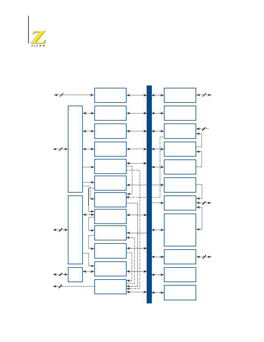
Figure 1 illustrates the architecture of the Z8FMC16100 Series Flash MCU.
Figure 1. Z8FMC16100 Series Flash MCU Block Diagram
Analog Supply
and Reference
UART with LIN
and IrDA
I
2
C
Master/Slave
SPI
Operational
Amplifier
A/D Converter
16-Bit Counter/
Timer/PWM
Digital Supply
Interrupt Control
Reset Control
Watch-Dog Timer
RC Oscillator
Internal Precision
Oscillator
Oscillator Control
Internal/External
Debugger
Register File (RAM)
512B x 8
Flash Program
Memory
Up to 16K x 8
Comparator
1
2
1
2
3
6
8
eZ8
20 MHz CPU
8
1
12-Bit PWM Module
for Motor Control
Port A
Port B
Port C
8-Channel
Multiplexer
Sample and Hold
Fault
Shutdown

PS024604-1005
P R E L I M I N A R Y
CPU and Peripheral Overview
Z8FMC16100 Series Flash MCU
Product Specification
3
CPU and Peripheral Overview
The eZ8 CPU, ZiLOG's latest 8-bit central processing unit, meets the continuing demand
for faster and more code-efficient microcontrollers. The eZ8 CPU executes a superset of
the original Z8
�
instruction set. The eZ8 CPU features include:
�
Direct register-to-register architecture allows each register to function as an accumula-
tor, improving execution time and decreasing the required program memory
�
Software stack allows much greater depth in subroutine calls and interrupts than hard-
ware stacks
�
Compatible with existing Z8
�
assembly code
�
New instructions improve execution efficiency for code developed using higher-level
programming languages, including C
�
Pipelined instruction fetch and execution
�
New instructions for improved performance including BIT, BSWAP, BTJ, CPC, LDC,
LDCI, LEA, MULT, and SRL
�
New instructions support 12-bit linear addressing of the Register File
�
Up to 10 MIPS operation
�
C-Compiler friendly
�
2-9 clock cycles per instruction
�
For more information regarding the eZ8 CPU, refer to the eZ8 CPU User Manual
(UM0128), available for download at
www.zilog.com
.
Pulse-Width Modulator for Motor Control Applications
To rotate a 3-phase motor three voltage and current signals must be supplied, each 120�
shifted from each other. To control a 3-phase motor the MCU must provide 6 PWM out-
puts.
The Z8FMC16100 Series Flash MCU features a flexible PWM module with three comple-
mentary pairs or six independent PWM outputs supporting deadband operation and fault
protection trip input. These features provide multiphase control capability for a variety of
motor types and ensure safe operation of the motor by providing immediate shutdown of
the PWM pins during fault condition.
10-Bit Analog-to-Digital Converter
The Z8FMC16100 Series Flash MCU devices feature up to eight channels of 10-bit A/D
conversion.

Introduction
P R E L I M I N A R Y PS024604-1005
Z8 Encore!
�
Motor Control Flash MCUs
Product Specification
4
Analog Comparator
The Z8FMC16100 Series Flash MCU features an on-chip analog comparator with external
input pins.
Operational Amplifier
The Z8FMC16100 Series Flash MCU features a two-input, one-output operational ampli-
fier.
General Purpose I/O
The Z8FMC16100 Series Flash MCU features 17 general purpose I/O (GPIO). Each pin is
individually programmable.
Flash Controller
The Flash Controller programs and erases the Flash memory. The Z8FMC16100 Series
Flash MCU products contain 16KB of on-chip Flash memory. A sector protection scheme
allows for flexible protection of user code.
Random Access Memory (RAM)
512B of internal RAM provides storage space for data, variables, and stack operations.
UART with LIN and IrDA
A full-duplex 9-bit UART provides serial, asynchronous communication and supports the
Local Interconnect Network (LIN) serial communications protocol. UART communica-
tion is full-duplex and capable of handling asynchronous data transfers. The UARTs sup-
port 8- and 9-bit data modes, selectable parity, and an efficient bus transceiver Driver
Enable signal for controlling a multitransceiver bus, such as RS-485. The LIN bus is a
cost-efficient single master, multiple slave organization that supports speeds up to 20K/
bits.
Serial Peripheral Interface
The serial peripheral interface (SPI) allows the Z8 Encore!
�
to exchange data between
other peripheral devices such as EEPROMs, A/D converters and ISDN devices. The SPI is
a full-duplex, synchronous, character-oriented channel that supports a four-wire interface.

PS024604-1005
P R E L I M I N A R Y I
2
C
Z8FMC16100 Series Flash MCU
Product Specification
5
I
2
C
The inter-integrated circuit (I
2
C) controller makes the Z8 Encore! compatible with the I
2
C
protocol. The I
2
C controller consists of two bidirectional bus lines, a serial data (SDA)
line and a serial clock (SCL) line. The I
2
C can operate as a master and/or slave and sup-
ports multimaster bus arbitration.
Internal Precision Oscillator
The Internal Precision Oscillator (IPO) provides a stable, accurate time base without the
requirement for external components. This can reduce system cost in many applications
by eliminating the requirement for external crystals or ceramic resonators. IPO frequency
is 5.5296MHz.
Crystal Oscillator
The on-chip crystal oscillator features programmable gain to support crystals and ceramic
resonators from 32KHz to 20MHz. The oscillator can also be used with clock drivers.
Standard Timer
The 16-bit reloadable timer can be used for timing/counting events and PWM signal gen-
eration. This timer provides a 16-bit programmable reload counter and operate in One-
Shot, Continuous, Gated, Capture, Compare, Capture and Compare, and PWM modes.
This timer can measure velocity from a tachometer wheel or read sensor outputs for rotor
position for brushless DC motor commutation. The standard timer can also be used for
general purpose timing and counting operations.
Interrupt Controller
The Z8FMC16100 Series Flash MCU products support 3 levels of programmable interrupt
priority. The interrupt sources include internal peripherals, general-purpose I/O pins, and
system fault detection.
Reset Controller
The Z8FMC16100 Series Flash MCU can be reset using the RESET pin, power-on reset,
Watch-Dog Timer (WDT), Stop-Mode Recovery, or Voltage Brown-Out (VBO) warning
signal.
On-Chip Debugger
The Z8FMC16100 Series Flash MCU features an integrated On-Chip Debugger (OCD).
The single-pin OCD interface provides a rich set of debugging capabilities, such as read-

Introduction
P R E L I M I N A R Y PS024604-1005
Z8 Encore!
�
Motor Control Flash MCUs
Product Specification
6
ing and writing registers, programming the Flash, setting break points and executing code.
OCD simplifies code development and allows easy in-circuit programming.

PS024604-1005
P R E L I M I N A R Y
Z8FMC16100 Series Flash MCU
Product Specification
7
Signal and Pin Descriptions
The Z8FMC16100 Series Flash MCU products are available in a variety of package styles
and pin configurations. This chapter describes the signals and available pin configurations
for each of the package styles. For information regarding the physical package specifica-
tions, please refer to the
Packaging
chapter on page 301.

Signal and Pin Descriptions
P R E L I M I N A R Y
PS024604-1005
Z8 Encore!
�
Motor Control Flash MCUs
Product Specification
8
Pin Configurations
Figure 2 illustrates the pin configuration for the packages available in the Z8FMC16100
Series Flash MCU. Refer to Table 1 for a description of the signals.
Figure 2. Z8FMC16100 Series Flash MCU in 32-Pin QFN and LQFP Package
PB2/ANA2/T0IN2
PB1/ANA1/T0IN1
PB0/ANA0/T0IN0
VREF
AVDD
1
AVSS
6
8
4
5
2
3
PA1/OPINP/CINN
PA3/TXDE/SCK /SCL
XIN
XOUT
PWM0L
VSS
24
PWM0h
18
17
20
19
22
21
PWM1H
PA2
/
CINP
PA7/FAULT1/T
0OUT
/ CO
MPOUT
RESET
/F
AULT0
PWM2L
DBG
9
PC0/T0OUT
14
16
12
13
10
11
PWM1L
PA4/RXD/MISO
PA5/TXD/MOSI
PA6/C
TS
/S
S
/SDA
PB5/A
NA5
PB7/A
NA7
25
PB6/A
NA6
30
32
28
29
26
27
PB3/A
NA3/
OPO
U
T
7
PA0/OPINN
15
PWM2H
VDD
23
31
PB4
/A
NA4
/
CI
N
N

PS024604-1005
P R E L I M I N A R Y Signal
Descriptions
Z8FMC16100 Series Flash MCU
Product Specification
9
Signal Descriptions
This section describes the Z8FMC16100 Series Flash MCU signals.
Table 1. Signal Descriptions
Signal Mnemonic
I/O
Description
General-Purpose I/O Ports A-H
PA[7:0]
I/O
Port A[7:0]. These pins are used for general-purpose I/O.
PB[7:0]
I/O
Port B[7:0]. These pins are used for general-purpose I/O.
PC[0]
I/O
Port C[0]. These pins are used for general-purpose I/O.
Pulse-Width Modulator for Motor Control
PWM0h/PWM1H
PWM2H
O
PWM High output.
PWM0L/PWM1L
PWM2L
O
PWM Low output.
FAULT0/FAULT1
I
PWM FAULT condition input. FAULT0 is active low, FAULT1 is active
high
SPI
MISO
I/O
Master In, Slave Out
MOSI
I/O
Master Out, Slave In.
SCLK
I/O
SPI Clock.
SS
I
Slave Select
Timers
T0OUT, T0OUT
O
General-Purpose Timer Outputs.
T0INx
I
General-Purpose Timer Input. This signal is used as the capture, gating
and counter inputs.
UART Controller
TXD
O
Transmit Data. This signal is the transmit output from the UART and
IrDA.
RXD
I
Receive Data. This signal is the receiver input for the UART and IrDA.
CTS
I
Clear To Send signal from the receiving device that ready to receive
data.
TXDE
O
Driver Enable. This signal allows automatic control of external RS-485
drivers. The DE signal may be used to ensure an external RS-485 driver
is enabled when data is transmitted by the UART.

Signal and Pin Descriptions
P R E L I M I N A R Y
PS024604-1005
Z8 Encore!
�
Motor Control Flash MCUs
Product Specification
10
Analog
ANA[7:0]
I
Analog Input. These signals are inputs to the analog-to-digital converter
(ADC).
V
REF
I/O
Voltage buffer output. This signal provides reference voltage for external
components.
If using the internal reference voltage generator, a 10 �F capacitor must
be placed on this pin to Ground.
CINP
I
Comparator positive input.
CINN
I
Comparator negative input.
COMPOUT
O
Comparator output.
OPINP
I
Operational amplifier positive input.
OPINN
I
Operational amplifier negative input.
OPOUT
O
Operational amplifier output.
Oscillators
X
IN
I
The External Crystal Input is the input pin to the crystal oscillator. A
crystal can be connected between it and the X
OUT
pin to form the
oscillator. In addition, this pin is used with external RC networks or
external clock drivers to provide the system clock.
X
OUT
O
External Crystal Output. This pin is the output of the crystal oscillator. A
crystal can be connected between it and the X
IN
pin to form the oscillator.
This pin must be left unconnected when not using a crystal.
On-Chip Debugger
DBG
I/O
Debug. This open-drain pin provides the single-pin control and data
interface to the On-Chip Debugger. For operation of the On-chip
Debugger, all power pins (V
DD
) must be supplied with power, and all
ground pins (V
SS
) must be grounded.
This pin is open-drain and must have an external pull-up resistor to
ensure proper operation.
Reset-PWM Fault
RESET/FAULT0
I/O
RESET input pin generates a Reset or PWM fault when asserted (driven
Low). The function selection is determined by the FLTSEL bit of the User
Options Bits at Program Memory Address 0001h, and the FAULTSEL bit
in the Reset Status and Control Register.
Table 1. Signal Descriptions (Continued)
Signal Mnemonic
I/O
Description
Caution
Caution

PS024604-1005
P R E L I M I N A R Y Pin
Characteristics
Z8FMC16100 Series Flash MCU
Product Specification
11
Pin Characteristics
Table 2 lists the characteristics for each of the Z8FMC16100 Series Flash MCU's 32 pins.
Data in Table 2 is sorted alphabetically by the pin symbol mnemonic.
Power Supply
VDD , AVDD
I
Power Supply.
VSS , AVSS
I
Ground.
Table 2. Pin Characteristics of the Z8FMC16100 Series Flash MCU
Symbol
Mnemonic Direction
Reset
Direction
Active Low
or
Active High
Tri-State
Output
Internal Pull-
up
or Pull-down
Schmitt
Trigger
Input
Open Drain
Output
DBG
I/O
I
N/A
Yes
Pull-up
Yes
Yes
PA[7:0]
I/O
I
N/A
Yes
Pull-up,
Programmable
Yes
Yes,
Programmable
PB[7:0]
I/O
I
N/A
Yes
Pull-up,
Programmable
Yes
Yes,
Programmable
PC[0]
I/O
I
N/A
Yes
Pull-up,
Programmable
Yes
Yes,
Programmable
PWMxH
I/O
Tristate
N/A
Yes
No
Yes
No
PWMxL
I/O
Tristate
N/A
Yes
No
Yes
No
RESET
I
I
Low
N/A
Pull-up
Yes
N/A
X
IN
I
I
N/A
N/A
No
No
N/A
V
REF
I/O
I
N/A
Yes
N/A
N/A
N/A
V
DD
, AV
DD
Supply
N/A
N/A
N/A
No
No
N/A
V
SS
, AV
SS
Supply
N/A
N/A
N/A
No
No
N/A
Note: x represents integer 0, 1,... to indicate multiple pins with symbol mnemonics that differ only by the integer.
Table 1. Signal Descriptions (Continued)
Signal Mnemonic
I/O
Description

Signal and Pin Descriptions
P R E L I M I N A R Y
PS024604-1005
Z8 Encore!
�
Motor Control Flash MCUs
Product Specification
12

PS024604-1005
P R E L I M I N A R Y Register
File
Z8FMC16100 Series Flash MCU
Product Specification
13
Address Space
The eZ8 CPU can access three distinct address spaces:
�
The Register File contains addresses for the general-purpose registers and the eZ8
CPU, peripheral, and general-purpose I/O port control registers.
�
The Program Memory contains addresses for all memory locations having executable
code and/or data.
�
The Data Memory contains addresses for all memory locations that hold data only.
These three address spaces are covered briefly in the following subsections. For more
detailed information regarding the eZ8 CPU and its address space, refer to the eZ8 CPU
User Manual (UM0128), available for download at
www.zilog.com
.
Register File
The Z8FMC16100 Series Flash MCU supports up to 512B of internal RAM within the
Register File address space.
The Register File is composed of two sections--control regis-
ters and general-purpose registers (RAM). When instructions are executed, registers are
read from when defined as sources and written to when defined as destinations. The archi-
tecture of the eZ8 CPU allows all general-purpose registers to function as accumulators,
address pointers, index registers, stack areas, or scratch pad memory.
The upper 256 bytes of the 4KB Register File address space are reserved for control of the
eZ8 CPU, the on-chip peripherals, and the I/O ports. These registers are located at
addresses from
F00h
to
FFFh
. Some of the addresses within the 256-byte control register
section are reserved (unavailable). Reading from an reserved Register File addresses
returns an undefined value.
Writing to reserved Register File addresses is not recommended and can produce unpre-
dictable results.
The on-chip RAM always begins at address
000h
in the Register File address space. The
Z8FMC16100 Series Flash MCU devices provide 512B of on-chip RAM depending upon
the device. Reading from Register File addresses outside the available RAM addresses
(and not within the control register address space) returns an undefined value. Writing to
these Register File addresses produces no effect. See the
Ordering Information for the
Z8FMC16100 Series Products*
section on page 303 to determine the amount of RAM
available for the specific Z8FMC16100 Series Flash MCU device.
Caution:

Address Space
P R E L I M I N A R Y
PS024604-1005
Z8 Encore!
�
Motor Control Flash MCUs
Product Specification
14
Program Memory
The Z8FMC16100 Series Flash MCU products contain 16 KB of on-chip Flash memory in
the Program Memory address space, depending upon the device (FMC08100 has 8 KB
and FMC04100 has 4 KB). Reading from Program Memory addresses outside the avail-
able Flash memory addresses returns
FFh
. Writing to these unimplemented Program
Memory addresses produces no effect. Table 3 describes the Program Memory Maps for
the Z8FMC16100 Series Flash MCU products.
Data Memory
The Z8FMC16100 Series Flash MCU does not use the eZ8 CPU's 64KB Data Memory
address space.
Information Area
Table 4 describes the Z8FMC16100 Series Flash MCU Information Area. This 512-byte
Information Area is accessed by setting bit 7 of the Flash Page Select Register to 1. When
access is enabled, the Information Area is mapped into the Program Memory and overlays
the 512 bytes at addresses
FE00h
to
FFFFh
. When the Information Area access is enabled,
execution of LDC and LDCI instruction from these Program Memory addresses return the
Information Area data rather than the Program Memory data. Reads of these addresses
through the On-Chip Debugger also returns the Information Area data. Execution of code
from these addresses continues to correctly use the Program Memory. Access to the Infor-
mation Area is read-only.
Table 3. Z8FMC16100 Series Flash MCU
Program Memory Maps
Program Memory Address (Hex)
Function
Z8FMC16000 Products
0000-0001
Option Bits
0002-0003
Reset Vector
0004-0007
System Exception Vectors
0008-003F
Interrupt Vectors
0040-3FFF
Program Memory
Note: See Table 29 on page 52 for a list of the interrupt vectors.

PS024604-1005
P R E L I M I N A R Y Information
Area
Z8FMC16100 Series Flash MCU
Product Specification
15
Table 4. Z8FMC16100 Series Information Area Map
Program Memory Address (Hex)
Function
FE00h�FE3Fh
Reserved.
FE40h�FE5Fh
Part Number
20-character ASCII alphanumeric code
Left justified and filled with zeros (ASCII Null
character).
FE60h�FFFFh
Reserved.

Address Space
P R E L I M I N A R Y
PS024604-1005
Z8 Encore!
�
Motor Control Flash MCUs
Product Specification
16

PS024604-1005
P R E L I M I N A R Y
Z8FMC16100 Series Flash MCU
Product Specification
17
Register File Address Map
Table 5 provides the address map for the Register File of the Z8FMC16100 Series Flash
MCU.
Table 5. Register File Address Map
Address
(Hex)
Register Description
Mnemonic
Reset (Hex)
Page #
General Purpose RAM--Z8FMC16 devices with 512B On-Chip RAM
000�1FF
General-Purpose Register File RAM
--
XX
13
200�EFF
Reserved
--
XX
Timer 0
F00
Timer 0 High Byte Register (T0H)
T0H
00
103
F01
Timer 0 Low Byte Register (T0L)
T0L
01
103
F02
Timer 0 Reload High Byte Register (T0RH)
T0RH
FF
104
F03
Timer 0 Reload Low Byte Register (T0RL)
T0RL
FF
104
F04
Timer 0 PWM High Byte Register (T0PWMH)
T0PWMH
00
105
F05
Timer 0 PWM Low Byte Register (T0PWML)
T0PWML
00
105
F06
Timer 0 Control 0 Register (T0CTL0)
T0CTL0
00
106
F07
Timer 0 Control 1 Register (T0CTL1)
T0CTL1
00
107
F08
ADC Timer 0 Capture Register, High Byte
ADCTCAP_H
XX
208
F09
ADC Timer 0 Capture Register, Low Byte
ADCTCAP_L
XX
209
F0A�F1F
Reserved
--
XX
Pulse-Width Modulator
F20
PWM Control 0 Register
PWMCTL0
00
78
F21
PWM Control 1 Register
PWMCTL1
00
80
F22
PWM Deadband Register
PWMDB
00
81
F23
PWM Minimum Pulse Width Filter
PWMMPF
00
82
F24
PWM Fault Mask Register
PWMFM
00
82
F25
PWM Fault Status Register
PWMFSTAT X0X0-0XXXb
83
Note: XX = undefined.

Register File Address Map
P R E L I M I N A R Y
PS024604-1005
Z8 Encore!
�
Motor Control Flash MCUs
Product Specification
18
F26
PWM Input Sample Register
PWMIN
00
86
F27
PWM Output Control Register
PWMOUT
00
87
F28
PWM Fault Control Register
PWMFCTL
00
85
F29
Current Sense ADC Trigger Control Register
PWMSHC
00
87
F2A�B
Reserved
--
XX
F2C
PWM High Byte Register (PWMH)
PWMH
00
75
F2D
PWM Low Byte Register (PWML)
PWML
00
76
F2E
PWM Reload High Byte Register (PWMRH)
PWMRH
0F
76
F2F
PWM Reload Low Byte Register (PWMRL)
PWMRL
FF
77
F30
PWM 0 High Side Duty Cycle High Byte
PWMH0Dh
00
77
F31
PWM 0 High Side Duty Cycle Low Byte
PWMH0DL
00
78
F32
PWM 0 Low Side Duty Cycle High Byte
PWML0Dh
00
77
F33
PWM 0 Low Side Duty Cycle Low Byte
PWML0DL
00
78
F34
PWM 1 High Side Duty Cycle High Byte
PWMH1DH
00
77
F35
PWM 1 High Side Duty Cycle Low Byte
PWMH1DL
00
78
F36
PWM 1 Low Side Duty Cycle High Byte
PWML1DH
00
77
F37
PWM 1 Low Side Duty Cycle Low Byte
PWML1DL
00
78
F38
PWM 2 High Side Duty Cycle High Byte
PWMH2DH
00
77
F39
PWM 2 High Side Duty Cycle Low Byte
PWMH2DL
00
78
F3A
PWM 2 Low Side Duty Cycle High Byte
PWML2DH
00
77
F3B
PWM 2 Low Side Duty Cycle Low Byte
PWML2DL
00
78
F3C�F3F
Reserved
--
XX
Table 5. Register File Address Map (Continued)
Address
(Hex)
Register Description
Mnemonic
Reset (Hex)
Page #
Note: XX = undefined.

PS024604-1005
P R E L I M I N A R Y
Z8FMC16100 Series Flash MCU
Product Specification
19
LIN-UART
F40
LIN-UART Transmit Data Register
U0TXD
XX
130
LIN-UART Receive Data Register
U0RXD
XX
130
F41
LIN-UART Status 0 Register
U0STAT0
0000_011Xb
131
F42
LIN-UART Control 0 Register
U0CTL0
00
134
F43
LIN-UART Control 1
U0CTL1
00
136
F44
LIN-UART Mode Select and Status
U0MDSTAT
00
133
F45
LIN-UART Address Compare
U0ADDR
00
140
F46
LIN-UART Baud Rate High Byte
U0BRH
FF
140
F47
LIN-UART Baud Rate Low Byte
U0BRL
FF
141
F48�F5F
Reserved
--
XX
I
2
C
F50
I2C Data Register
I2CDATA
00
184
F51
I2C Interrupt Status Register
I2CISTAT
80
184
F52
I2C Control Register
I2CCTL
00
186
F53
I2C Baud Rate High Byte Register (I2CBRH)
I2CBRH
FF
188
F54
I2C Baud Rate Low Byte Register (I2CBRL)
I2CBRL
FF
188
F55
I2C State Register (I2CSTATE) - Description
when DIAG = 0
I2CSTATE
0X
189
I2C State Register (I2CSTATE) - Description
when DIAG = 1
I2CSTATE
00
190
F56
I2C Mode Register
I2CMODE
00
192
F57
I2C Slave Address Register
I2CSLVAD
00
193
F58�F5F
Reserved
--
XX
SPI
F60
SPI Data Register
SPIDATA
XX
157
F61
SPI Control Register
SPICTL
00
158
F62
SPI Status Register
SPISTAT
01
159
Table 5. Register File Address Map (Continued)
Address
(Hex)
Register Description
Mnemonic
Reset (Hex)
Page #
Note: XX = undefined.

Register File Address Map
P R E L I M I N A R Y
PS024604-1005
Z8 Encore!
�
Motor Control Flash MCUs
Product Specification
20
F63
SPI Mode Register
SPIMODE
00
160
F64
SPI Diagnostic State Register
SPIDST
00
161
F65
Reserved
--
XX
F66
SPI Baud Rate High Byte Register (SPIBRH)
SPIBRH
FF
162
F67
SPI Baud Rate Low Byte Register (SPIBRL)
SPIBRL
FF
162
F68�F6F
Reserved
--
XX
Analog-to-Digital Converter (ADC)
F70
ADC Control Register 0
ADCCTL0
20
203
F71
ADC Raw Data High Byte Register
ADCRD_H
XX
204
F72
ADC Data High Byte Register
ADCD_H
XX
204
F73
ADC Data Low Bits Register
ADCD_L
XX
205
F74
Sample Settling Time Register
ADCSST
1F
206
F75
Sample Time Register
ADCST
A0
206
F76
ADC Clock Prescale Register
ADCCP
00
207
F77�F85
Reserved
--
XX
Oscillator Control
F86
Oscillator Control Register
OSCCTL
A0
233
F87
Oscillator Divide Register
OSCDIV
00
234
Trim Control
F88�F8F
Reserved
--
XX
Comparator and Op Amp
F90
Comparator and Op Amp Control Register
CMPOPC
00
197
F91�FBF
Reserved
--
XX
Interrupt Controller
FC0
Interrupt Request 0 Register
IRQ0
00
55
FC1
IRQ0 Enable High Bit Register (IRQ0ENH)
IRQ0ENH
00
58
FC2
IRQ0 Enable Low Bit Register (IRQ0ENL)
IRQ0ENL
00
59
Table 5. Register File Address Map (Continued)
Address
(Hex)
Register Description
Mnemonic
Reset (Hex)
Page #
Note: XX = undefined.
PS024604-1005
P R E L I M I N A R Y
Z8FMC16100 Series Flash MCU
Product Specification
21
FC3
Interrupt Request 1 Register
IRQ1
00
57
FC4
IRQ1 Enable High Bit Register (IRQ1ENH)
IRQ1ENH
00
60
FC5
IRQ1 Enable Low Bit Register (IRQ1ENL)
IRQ1ENL
00
60
FC9�FCE Reserved
--
XX
FCF
Interrupt Control Register
IRQCTL
00
61
GPIO Port A
FD0
Port A Address
PAADDR
00
40
FD1
Port A Control
PACTL
00
41
FD2
Port A Input Data
PAIN
XX
48
FD3
Port A Output Data
PAOUT
00
49
GPIO Port B
FD4
Port B Address
PBADDR
00
40
FD5
Port B Control
PBCTL
00
41
FD6
Port B Input Data
PBIN
XX
48
FD7
Port B Output Data
PBOUT
00
49
GPIO Port C
FD8
Port C Address
PCADDR
00
40
FD9
Port C Control
PCCTL
00
41
FDA
Port C Input Data
PCIN
XX
48
FDB
Port C Output Data
PCOUT
00
49
Reset and Watch-Dog Timer (WDT)
FF0
Reset Status and Control Register
RSTSTAT
see Table 10
29
FF1
Reserved
--
XX
FF2
Watch-Dog Timer Reload High Byte Register
(WDTH)
WDTH
04
66
FF3
Watch-Dog Timer Reload Low Byte Register
(WDTL)
WDTL
00
66
FF4�FF5
Reserved
--
XX
Table 5. Register File Address Map (Continued)
Address
(Hex)
Register Description
Mnemonic
Reset (Hex)
Page #
Note: XX = undefined.

Register File Address Map
P R E L I M I N A R Y
PS024604-1005
Z8 Encore!
�
Motor Control Flash MCUs
Product Specification
22
Trim
FF6
Trim Bit Address Register
TRMADR
00
227
FF7
Trim Bit Data Register
TRMDR
00
227
Flash Memory Controller
FF8
Flash Control Register
FCTL
00
217
FF8
Flash Status Register
FSTAT
00
218
FF9
Flash Page Select Register
FPS
00
218
FF9 (if
enabled)
Flash Sector Protect Register
FPROT
00
219
FFA
Flash Frequency High Byte Register
(FFREQH)
FFREQH
00
220
FFB
Flash Frequency Low Byte Register (FFREQL)
FFREQL
00
221
eZ8 CPU
FFC
Flags
FLAGS
XX
Refer to the
eZ8 CPU
User Manual
(UM0128).
FFD
Register Pointer
RP
XX
FFE
Stack Pointer High Byte
SPH
XX
FFF
Stack Pointer Low Byte
SPL
XX
Table 5. Register File Address Map (Continued)
Address
(Hex)
Register Description
Mnemonic
Reset (Hex)
Page #
Note: XX = undefined.

PS024604-1005
P R E L I M I N A R Y Reset
Types
Z8FMC16100 Series Flash MCU
Product Specification
23
Reset and Stop-Mode Recovery
The Reset Controller within the Z8FMC16100 Series Flash MCU controls RESET and
Stop-Mode Recovery operation. In typical operation, the following events cause a RESET
to occur:
�
Power-On Reset (POR)
�
Voltage Brown-Out (VBO)
�
Watch-Dog Timer time-out (when configured via the
WDT_RES
Option Bit to initiate a
Reset)
�
External RESET pin assertion
�
On-Chip Debugger initiated RESET (
OCDCTL[0]
set to 1)
�
Fault detect logic
When the Z8FMC16100 Series Flash MCU is in STOP mode, a Stop-Mode Recovery is
initiated by either of the following:
�
Watch-Dog Timer time-out
�
GPIO port input pin transition on an enabled Stop-Mode Recovery source
Reset Types
The Z8FMC16100 Series Flash MCU provides two different types of reset operation (Sys-
tem Reset and Stop-Mode Recovery). The type of reset is a function of both the current
operating mode of the Z8FMC16100 Series Flash MCU and the source of the reset. Table
6 lists the types of reset and their operating characteristics.
Table 6. Reset and Stop-Mode Recovery Characteristics and Latency
Reset Type
Reset Characteristics and Latency
Peripheral Control
Registers
eZ8 CPU Reset Latency (Delay)
System Reset
Reset (as
applicable)
RESET
A minimum of 66 Internal Precision Oscillator cycles.
Stop-Mode
Recovery
Unaffected, except
RSTSRC and
OSCCTL registers
Reset
A minimum of 66 Internal Precision Oscillator cycles.

Reset and Stop-Mode Recovery
P R E L I M I N A R Y
PS024604-1005
Z8 Encore!
�
Motor Control Flash MCUs
Product Specification
24
System Reset
During a system reset, the Z8FMC16100 Series Flash MCU is held in RESET for 66
cycles of the Internal Precision Oscillator. At the beginning of RESET, all GPIO pins are
configured as inputs. All GPIO programmable pull-ups are disabled.
At the start of a System Reset, the motor control PWM outputs are forced to high-imped-
ance momentarily. When the Option Bits that control the off-state have been properly
evaluated the PWM outputs are forced to the programmed off-state.
During RESET, the eZ8 CPU and on-chip peripherals are idle; however, the Internal Preci-
sion Oscillator and Watch-Dog Timer oscillator continue to run. During the first 50 clock
cycles the internal option bit registers are initialized, after which the system clock for the
core and peripherals begins operating. The eZ8 CPU and on-chip peripherals remain idle
through the next 16 cycles of the system clock after which time the internal reset signal is
deasserted.
Upon RESET, control registers within the Register File that have a defined reset value are
loaded with their reset values. Other control registers (including the Flags) and general-
purpose RAM are undefined following RESET. The eZ8 CPU fetches the RESET vector
at Program Memory addresses
0002h
and
0003h
and loads that value into the Program
Counter. Program execution begins at the RESET vector address.
Table 7 lists the system reset sources as a function of the operating mode. The text follow-
ing provides more detailed information on the individual RESET sources. Please note that
a Power-On Reset/Voltage Brown-Out event always has priority over all other possible
reset sources to ensure a full system reset occurs.
Table 7. System Reset Sources and Resulting Reset Action
Operating Mode System Reset Source
Action
Normal or HALT
modes
Power-On Reset/Voltage Brown-Out
System Reset.
Watch-Dog Timer time-out when
configured for reset.
System Reset.
RESET pin assertion.
System Reset.
Write OCDCTL[0] to 1.
System Reset except the On-Chip
Debugger is not reset.
Fault detect logic reset.
System Reset.
STOP mode
Power-On Reset/Voltage Brown-Out.
System Reset.
RESET pin assertion.
System Reset.
Fault detect logic reset.
System Reset.
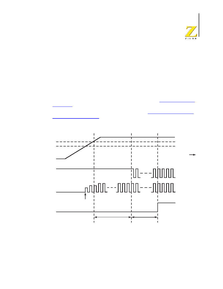
PS024604-1005
P R E L I M I N A R Y Power-On
Reset
Z8FMC16100 Series Flash MCU
Product Specification
25
Power-On Reset
Each device in the Z8FMC16100 Series Flash MCU contains an internal Power-On Reset
(POR) circuit. The POR circuit monitors the supply voltage and holds the device in the
Reset state until the supply voltage reaches a safe operating level. After the supply voltage
exceeds the POR voltage threshold (V
POR
) and has stabilized, the POR Counter is enabled
and counts 50 cycles of the Internal Precision Oscillator. At this point the System Clock is
enabled and the POR Counter counts a total of 16 system clock pulses. The device is held
in the Reset state until this second POR Counter sequence has timed out. After the
Z8FMC16100 Series Flash MCU exits the Power-On Reset state, the eZ8 CPU fetches the
Reset vector. Following Power-On Reset, the
POR
status bit in the
Reset Status and Con-
trol Register
is set to 1.
Figure 3 illustrates Power-On Reset operation. Refer to the
On-Chip Peripheral AC and
DC Electrical Characteristics
section on page 265
for the POR threshold voltage
(V
POR
).
Voltage Brown-Out Reset
The Z8FMC16100 Series Flash MCU provides low Voltage Brown-Out (VBO) protection.
The VBO circuit senses when the supply voltage drops to an unsafe level (below the VBO
Figure 3. Power-On Reset Operation
Option Bit
Counter Delay
Oscillator
Startup
System Clock
Counter Delay
Internal RESET
Signal
Internal Precision
Oscillator
System Clock
V
CC
= 0.0V
V
CC
= 3.3V
V
VBO
V
POR
Program Execution
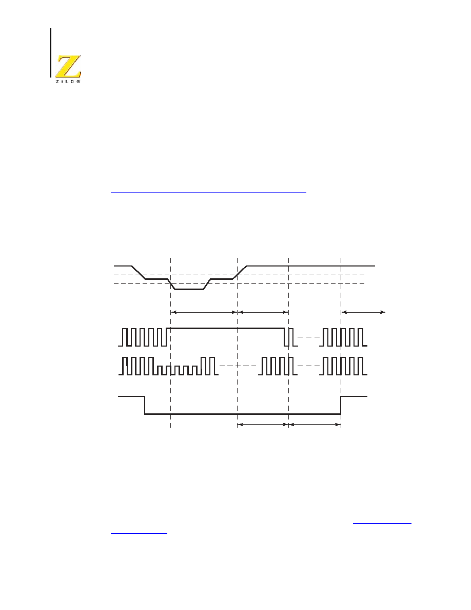
Reset and Stop-Mode Recovery
P R E L I M I N A R Y
PS024604-1005
Z8 Encore!
�
Motor Control Flash MCUs
Product Specification
26
threshold voltage) and forces the device into the Reset state. While the supply voltage
remains below the Power-On Reset voltage threshold (V
POR
), the VBO holds the device in
the Reset state.
After the supply voltage again exceeds the Power-On Reset voltage threshold and stabi-
lized, the device progresses through a full System Reset sequence, as described in the
Power-On Reset section. Following Power-On Reset, the
POR
status bit in the Reset
Source
register is set to 1. Figure 4 illustrates Voltage Brown-Out operation. Refer to the
On-Chip Peripheral AC and DC Electrical Characteristics
section on page 265
for the
VBO and POR threshold voltages (V
VBO
and V
POR
).
The Voltage Brown-Out circuit can be either enabled or disabled during STOP mode.
Operation during STOP mode is controlled by the
VBO_AO
Option Bit. Refer to the Option
Bits chapter for information on configuring
VBO_AO
.
Watch-Dog Timer Reset
If the device is in normal or HALT mode, the Watch-Dog Timer can initiate a System
Reset at time-out if the
WDT_RES
Option Bit is set to 1. This setting is the default (unpro-
grammed) setting of the
WDT_RES
Option Bit. The
WDT
status bit in the
Reset Status and
Control Register
is set to signify that the reset was initiated by the Watch-Dog Timer.
Figure 4. Voltage Brown-Out Reset Operation
Option Bit
Counter Delay
System Clock
Counter Delay
Internal RESET
Signal
Internal Precision
Oscillator
System Clock
V
CC
= 3.3V
V
CC
= 3.3V
V
VBO
V
POR
Program Execution
Program
Execution
Voltage
Brown-Out

PS024604-1005
P R E L I M I N A R Y
External Pin Reset
Z8FMC16100 Series Flash MCU
Product Specification
27
External Pin Reset
The input-only RESET pin has a Schmitt-triggered input, an internal pull-up, an analog
filter and a digital filter to reject noise. Once the RESET pin is asserted for at least 4 sys-
tem clock cycles, the device progresses through the System Reset sequence. While the
RESET input pin is asserted Low, the Z8FMC16100 Series Flash MCU device continues
to be held in the Reset state. If the RESET pin is held Low beyond the System Reset time-
out, the device exits the Reset state 16 system clock cycles following RESET pin deasser-
tion. If the RESET pin is released before the System Reset time-out, the RESET pin is
driven Low by the chip until the completion of the time-out as described in the next sec-
tion. In STOP mode the digital filter is bypassed because the System Clock is disabled.
Following a System Reset initiated by the external RESET pin, the
EXT
status bit in the
Reset Status and Control Register
is set to 1.
External Reset Indicator
During System Reset, the RESET pin functions as an open drain (active Low) reset mode
indicator in addition to the input functionality. This reset output feature allows a
Z8FMC16100 Series Flash MCU device to reset other components to which it is con-
nected, even if the reset is caused by internal sources such as POR, VBO, or WDT events
and as an indication of when the reset sequence completes.
Once an internal reset event occurs, the internal circuitry begins driving the RESET pin
Low. The RESET pin is held Low by the internal circuitry until the appropriate delay
listed in Table 6 has elapsed.
On-Chip Debugger Initiated Reset
A System Reset may be initiated via the On-Chip Debugger by setting
RST
bit of the
OCDCTL register. The On-Chip Debugger is not reset but the rest of the chip goes
through a normal system reset. The
RST
bit automatically clears during the system reset.
Following the system reset, the
POR
bit in the
Reset Status and Control Register
is set.
Fault Detect Logic Reset
Fault detect circuitry exists to detect illegal state changes which may be caused by tran-
sient power or electrostatic discharge events. When such a fault is detected, a system reset
is forced. Following the system reset, the
FLTD
bit in the
Reset Status and Control Register
is set.

Reset and Stop-Mode Recovery
P R E L I M I N A R Y
PS024604-1005
Z8 Encore!
�
Motor Control Flash MCUs
Product Specification
28
Stop-Mode Recovery
STOP mode is entered by execution of a
STOP
instruction by the eZ8 CPU. Refer to the
Low-Power Modes
chapter on page 31 for detailed STOP mode information. During Stop-
Mode Recovery, the device is held in reset for 66 cycles of the Internal Precision Oscilla-
tor. Stop-Mode Recovery only affects the contents of the
Reset Status and Control Regis-
ter
and
Oscillator Control Register
. Stop-Mode Recovery does not affect any other values
in the Register File, including the Stack Pointer, Register Pointer, Flags, peripheral control
registers, and general-purpose RAM.
The eZ8 CPU fetches the Reset vector at Program Memory addresses
0002h
and
0003h
and loads that value into the Program Counter. Program execution begins at the Reset vec-
tor address. Following Stop-Mode Recovery, the
STOP
bit in the
Reset Status and Control
Register
is set to 1. Table 8 lists the Stop-Mode Recovery sources and resulting actions.
The text following provides more detailed information on each of the Stop-Mode Recov-
ery sources
Stop-Mode Recovery Using Watch-Dog Timer Time-Out
If the Watch-Dog Timer times out during STOP mode, the device undergoes a Stop-Mode
Recovery sequence. In the
Reset Status and Control Register
, the
WDT
and
STOP
bits are
set to 1. If the Watch-Dog Timer is configured to generate a System Exception upon time-
out, the eZ8 CPU services the Watch-Dog Timer System Exception following the normal
Stop-Mode Recovery sequence.
Stop-Mode Recovery Using a GPIO Port Pin Transition
Each of the GPIO port pins may be configured as a Stop-Mode Recovery input source. On
any GPIO pin enabled as a Stop-Mode Recovery source, a change in the input pin value
(from High to Low or from Low to High) initiates Stop-Mode Recovery. The GPIO Stop-
Mode Recovery signals are filtered to reject pulses less than 10ns (typical) in duration. In
the
Reset Status and Control Register
, the STOP bit is set to 1.
Table 8. Stop-Mode Recovery Sources and Resulting Action
Operating Mode
Stop-Mode Recovery Source
Action
Stop Mode
Watch-Dog Timer time-out when
configured for Reset
Stop-Mode Recovery
Watch-Dog Timer time-out when
configured for System Exception
Stop-Mode Recovery followed by WDT
System Exception
Data transition on any GPIO port pin
enabled as a Stop-Mode Recovery
source
Stop-Mode Recovery

PS024604-1005
P R E L I M I N A R Y
PWM Fault0 and Reset pin selection
Z8FMC16100 Series Flash MCU
Product Specification
29
Short pulses on the Port pin can initiate Stop-Mode Recovery without initiating an in-
terrupt (if enabled for that pin).
PWM Fault0 and Reset pin selection
The RESET pin can be set to function as a PWM Fault input. When selected, the RESET
input function is disabled. The
FLTSEL
bit in the
Reset Status and Control Register
allows
software selection of the RESET pin function. The pin function is selected by writing the
the unlock sequence followed by the mode to this register. A software write to the
FLTSEL
bit will override the value set by the
FLTSEL
user option bit
Reset Control Register Definitions
Writing the
14h
,
92h
unlock sequence to the Reset Status and Control Register address
unlocks access to the
FLTSEL
bit. The locking mechanism prevents spurious writes to this
bit. The following sequence is required to unlock this register and write the
FLTSEL
bit.
1. Write
14h
to the Reset Status and Control Register (RSTSTAT).
2. Write
92h
to the Reset Status and Control Register (RSTSTAT).
3. Write the
FLTSEL
bit.
All steps of the unlock sequence must be written in the order listed.
Reset Status and Control Register
The Reset Status (RSTSTAT) Register, shown in Table 9, records the cause of the most
recent Reset or Stop-Mode Recovery. All status bits are updated on each Reset or Stop-
Mode Recovery event. Table 10 indicates the possible states of the Reset status bits fol-
lowing a Reset or Stop-Mode Recovery event. The RESET pin function is also select with
FLTSEL
bit.
Caution:
Reset and Stop-Mode Recovery
P R E L I M I N A R Y
PS024604-1005
Z8 Encore!
�
Motor Control Flash MCUs
Product Specification
30
The
FLTSEL
bit in this register allows software selection of the RESET pin. The pin func-
tion is selected by writing the unlock sequence followed by the mode to this register. A
software write to the
FLTSEL
bit will override the value set by the
FLTSEL
user option bit.
0 =
RESET/Fault0 pin is configured as RESET input.
1=
RESET/Fault0 pin is configured as Fault0 input.
Table 9. Reset Status and Control Register (RSTSCR)
BITS
7
6
5
4
3
2
1
0
FIELD
POR
STOP
WDT
EXT
FLT
Reserved
FLTSEL
RESET
See Table 10 below
0
R/W
R
R
R
R
R
R
R/W
ADDR
FF0H
Table 10. Reset Status Register Values Following Reset
Reset or Stop-Mode Recovery Event
POR
STOP
WDT
EXT
FLT
Power-On Reset
1
0
0
0
0
Reset using RESET pin assertion
0
0
0
1
0
Reset using Watch-Dog Timer time-out
0
0
1
1
0
Reset by OCD writing OCDCTL[0] to 1
1
0
0
1
0
Reset from Fault Detect Logic
0
0
0
1
1
Stop-Mode Recovery using GPIO pin transition
0
1
0
0
0
Stop-Mode Recovery using Watch-Dog Timer time-out
0
1
1
0
0
Note: Additional bits may be set depending on the number of resets simultaneously occurring.

PS024604-1005
P R E L I M I N A R Y Stop
Mode
Z8FMC16100 Series Flash MCU
Product Specification
31
Low-Power Modes
The Z8FMC16100 Series Flash MCU products contain power-saving features. The high-
est level of power reduction is provided by STOP mode. The next level of power reduction
is provided by the HALT mode.
Stop Mode
Execution of the eZ8 CPU's STOP instruction places the Z8FMC16100 Series Flash MCU
into STOP mode. In STOP mode, the operating characteristics are:
�
Primary crystal oscillator and IPO are stopped; XIN and XOUT pins are driven to V
SS
.
�
System clock is stopped
�
eZ8 CPU is stopped
�
Program counter (PC) stops incrementing
�
If enabled for operation during STOP mode, the Watch-Dog Timer and its internal RC
oscillator continue to operate.
�
If enabled for operation in STOP mode through the associated Option Bit, the Voltage
Brown-Out protection circuit continues to operate.
�
Comparators and voltage reference operate unless disabled.
�
All other on-chip peripherals are idle
To minimize current in STOP mode, all GPIO pins that are configured as digital inputs
must be driven to one of the supply rails (V
CC
or GND), the Voltage Brown-Out protection
and the Watch-Dog Timer must be disabled. The device can be brought out of STOP mode
using Stop-Mode Recovery. For more information refer to the
Reset and Stop-Mode
Recovery
chapter on page 23.
To prevent excess current consumption, STOP mode must not be used if the device is
driven with an external clock source.
Halt Mode
Execution of the eZ8 CPU's HALT instruction places the device into HALT mode. In
HALT mode, the operating characteristics are:
�
Primary crystal oscillator is enabled and continues to operate
Caution:

Low-Power Modes
P R E L I M I N A R Y
PS024604-1005
Z8 Encore!
�
Motor Control Flash MCUs
Product Specification
32
�
System clock is enabled and continues to operate
�
eZ8 CPU is stopped
�
Program counter (PC) stops incrementing
�
Watch-Dog Timer's internal RC oscillator continues to operate
�
If enabled, the Watch-Dog Timer continues to operate
�
All other on-chip peripherals continue to operate
The eZ8 CPU can be brought out of HALT mode by any of the following operations:
�
Interrupt or System Exception
�
Watch-Dog Timer time-out (System Exception or reset)
�
Power-on reset
�
Voltage-brown out reset
�
External RESET pin assertion
�
Halt Mode Recovery time is less than 5 �s.
To minimize current in HALT mode, all GPIO pins which are configured as inputs must be
driven to one of the supply rails (V
CC
or GND).
Peripheral-Level Power Control
In addition to the STOP and HALT modes, it is possible to disable unused on-chip analog
peripherals of the Z8FMC16100 Series Flash MCU device during operation. Disabling an
unused analog peripheral minimizes power consumption. Power consumption of the
unused on-chip digital peripherals is automatically minimized when not in use.

PS024604-1005
P R E L I M I N A R Y
Power Control Register 0
Z8FMC16100 Series Flash MCU
Product Specification
33
Power Control Register 0
Each bit of the following registers disables a peripheral block, either by gating its system
clock input or by removing power from the block.
Table 11. Power Control Register 0(PWRCTL0)
BITS
7
6
5
4
3
2
1
0
FIELD
Reserved Reserved Reserved
VBODIS
Reserved Reserved Reserved Reserved
RESET
0
0
0
0
0
0
0
0
R/W
R/W
R/W
R/W
R/W
R/W
R/W
R/W
R/W
ADDR
F80H
Bit
Position
Value
(H)
Description
[7:5]
Reserved
Must be 0.
[4]
VBODIS
0
Voltage Brownout Detector Disable
(This bit and the VBO_AO Option Bit must be enabled for the VBO to be active.
Voltage Brownout Detector is enabled.
1
Voltage Brownout Detector is disabled.
[3:0]
Reserved
Must be 0.

Low-Power Modes
P R E L I M I N A R Y
PS024604-1005
Z8 Encore!
�
Motor Control Flash MCUs
Product Specification
34

PS024604-1005
P R E L I M I N A R Y
GPIO Port Availability By Device
Z8FMC16100 Series Flash MCU
Product Specification
35
General-Purpose I/O
The Z8FMC16100 Series Flash MCU contains general-purpose input/output pins (GPIO)
arranged as Ports A�C. Each port contains control and data registers. The GPIO control
registers are used to determine data direction, open-drain, output drive current, pull-up,
and alternate pin functions. Each port pin is individually programmable.
GPIO Port Availability By Device
Table 12 lists the port pins available with each device and package type.
Architecture
Figure 5 illustrates a simplified block diagram of a GPIO port pin. In this figure, the abil-
ity to accommodate alternate functions and variable port current drive strength are not
illustrated.
Table 12. Port Availability by Device and Package Type
Package
Port A
Port B
Port C
32-pin
[7:0]
[7:0]
[0]

General-Purpose I/O
P R E L I M I N A R Y
PS024604-1005
Z8 Encore!
�
Motor Control Flash MCUs
Product Specification
36
GPIO Alternate Functions
Many of the GPIO port pins can be used as both general-purpose I/O and to provide access
to on-chip peripheral functions, such as timers and serial communication devices. The Port
A-C Alternate Function subregisters configure these pins for either general-purpose I/O or
alternate function operation. When a pin is configured for alternate function, control of the
port pin direction (input/output) is passed from the Port A-C Data Direction registers to
the alternate function assigned to this pin. For peripherals with digital input alternate func-
tions (for example, a Timer input T0IN0), selecting the alternate function is not required.
Table 13 lists the alternate functions associated with each port pin and the required alter-
nate function (AF0 and AF1) subregister settings. In general, enabling an analog alternate
Figure 5. GPIO Port Pin Block Diagram
System Clock
Data Bus
D
Q
D
Q
Pull-Up Enable
Schmitt Trigger
Port
Pin
GND
V
DD
Port Input
Data Register
Port Output
Data Register
System Clock
Port Output Control
Port Data Direction
Analog In/Out
On-Chip
Peripheral
Alternate Function
Digital Input

PS024604-1005
P R E L I M I N A R Y
GPIO Alternate Functions
Z8FMC16100 Series Flash MCU
Product Specification
37
function automatically disables the digital Schmitt-trigger input for the associated port
input.
Table 13. Port Alternate Function Mapping
Port
Pin
Mnemonic
AF0
AF1 Alternate Function Description
Port A
PA7
PA7
0
0
GPIO.
T0OUT
0
1
Timer 0 output (active Low).
FAULT1
1
0
Fault Input.
COMPOUT
1
1
Comparator output.
PA6
PA6
0
0
GPIO.
SS
0
1
SPI Slave Select.
CTS
1
0
UART Clear to Send.
SDA
1
1
I
2
C Serial Data.
PA5
PA5
0
0
GPIO.
MOSI
0
1
SPI Master Out Slave In.
TXD
1
0
UART Transmit data.
1
1
Reserved; do not use.
PA4
PA4
0
0
GPIO.
MISO
0
1
SPI Master In Slave Out.
RXD
1
0
UART Receive data.
1
1
Reserved; do not use.
PA3
PA3
0
0
GPIO.
SCK
0
1
SPI Serial Clock.
TXDE
1
0
UART Driver Enable.
SCL
1
1
I
2
C serial clock.
PA2
PA2
0
0
GPIO.
0
1
Reserved; do not use.
CINP
1
0
Comparator Positive Input.
1
1
Reserved; do not use.

General-Purpose I/O
P R E L I M I N A R Y
PS024604-1005
Z8 Encore!
�
Motor Control Flash MCUs
Product Specification
38
Port A
PA1
PA1
0
0
GPIO.
0
1
Reserved; do not use.
OPINP and CINN
1
0
Op amp positive input and comparator negative
input.
1
1
Reserved; do not use.
PA0
PA0
0
0
GPIO.
0
1
Reserved; do not use.
OPINN
1
0
Op amp negative input.
1
1
Reserved; do not use.
Port B
PB7
PB7
0
0
GPIO.
0
1
Reserved; do not use.
ANA7
1
0
ADC analog input 7.
1
1
Reserved; do not use.
PB6
PB6
0
0
GPIO.
0
1
Reserved; do not use.
ANA6
1
0
ADC analog input 6.
1
1
Reserved; do not use.
PB5
PB5
0
0
GPIO.
0
1
Reserved; do not use.
ANA5
1
0
ADC analog input 5.
1
1
Reserved; do not use.
PB4
PB4
0
0
GPIO.
0
1
Reserved; do not use.
ANA4
1
0
ADC analog input 4 (also CINN if CPSEL=1).
1
1
Reserved; do not use.
PB3
PB3
0
0
GPIO.
PB3INT
0
1
GPIO with edge interrupt.
ANA3 and OPOUT
1
0
ADC analog input 3 and op amp output.
1
1
Reserved; do not use.
Table 13. Port Alternate Function Mapping (Continued)
Port
Pin
Mnemonic
AF0
AF1 Alternate Function Description

PS024604-1005
P R E L I M I N A R Y GPIO
Interrupts
Z8FMC16100 Series Flash MCU
Product Specification
39
GPIO Interrupts
Many of the GPIO port pins can be used as interrupt sources. The Port A[7:0] pins can be
configured to generate an interrupt request on either the rising edge or falling edge of the
pin input signal. The Port B[3:0] pins can be configured to generate an interrupt request on
both the rising and falling edges of the pin input signal. For Port A, the GPIO interrupt
edge selection is controlled by the Interrupt Edge Select subregister. Enabling and dis-
abling of the Port Interrupts is handled in the Interrupt Controller. Port B[3:0], with dual
edge interrupt capability, is selected by AF1, AF0. Refer to the
Interrupt Controller
chap-
ter on page 51 for more information.
GPIO Control Register Definitions
Four registers for each Port provide access to GPIO control, input data, and output data.
Table 14 lists these Port registers. Use the Port A�C Address and Control registers
together to provide access to subregisters for Port configuration and control.
Port B
PB2
PB2
0
0
GPIO/Timer 0 input 2.
PB2INT
0
1
GPIO/Timer 0 input 2--edge interrupt enabled.
ANA2
1
0
ADC analog input 2.
T0IN2
1
1
Timer 0 input 2; dedicated input.
PB1
PB1
0
0
GPIO/Timer 0 input 1.
PB1INT
0
1
GPIO/Timer 0 input 1--edge interrupt enabled.
ANA1
1
0
ADC analog input 1.
1
1
Reserved; do not use.
PB0
PB0
0
0
GPIO/Timer 0 input 0.
PB0INT
0
1
GPIO/Timer 0 input 0--edge interrupt enabled.
ANA0
1
0
ADC analog input 0.
1
1
Reserved; do not use.
Port C
PC0
PC0
0
0
GPIO.
0
1
Reserved; do not use.
T0OUT
1
0
Timer 0 output.
1
1
Reserved; do not use.
Table 13. Port Alternate Function Mapping (Continued)
Port
Pin
Mnemonic
AF0
AF1 Alternate Function Description
General-Purpose I/O
P R E L I M I N A R Y
PS024604-1005
Z8 Encore!
�
Motor Control Flash MCUs
Product Specification
40
Port A-C Address Registers
The Port A�C Address registers select the GPIO port functionality accessible through the
Port A�C Control registers. The Port A�C Address and Control registers combine to pro-
vide access to all GPIO port control. See Table 15.
Table 16 lists the Port Control subregisters that are accessible via the Port A�C Control
registers.
Table 14. GPIO Port Registers and Subregisters
Port Register Mnemonic
Port Register Name
PxADDR
Port A�C Address Register--selects subregisters.
PxCTL
Port A�C Control Register--provides access to
subregisters.
PxIN
Port A�C Input Data Register.
PxOUT
Port A�C Output Data Register.
Port Subregister Mnemonic
Port Register Name
PxDD
Data Direction
PxAF0
Alternate Function 0
PxAF1
Alternate Function 1--Ports A and B only.
PxOC
Output Control (open-drain).
PxHDE
High Drive Enable.
PxSMRE
Stop-Mode Recovery Source Enable.
PxPUE
Pull-Up Enable.
PxIRQES
Interrupt Edge Select--Ports A and C only.
IRQPSEL
Interrupt Port Select--Port A only.
Table 15. Port A�C GPIO Address Registers (PxADDR)
BITS
7
6
5
4
3
2
1
0
FIELD
PADDR[7:0]
RESET
00H
R/W
R/W
ADDR
FD0H, FD4H, FD8H
PS024604-1005
P R E L I M I N A R Y
Port A�C Control Registers
Z8FMC16100 Series Flash MCU
Product Specification
41
Port A�C Control Registers
The Port A�C Control registers set the GPIO port operation. The value in the correspond-
ing Port A�C Address register determines the control subregisters accessible using the
Port A�C Control registers, shown in Table 17. The Port Control registers provide access
to all subregisters that configure GPIO port operation.
Port A�C Data Direction Subregisters
The Port A�C Data Direction subregisters are accessed through the Port A�C Control reg-
isters by writing
01h
to the Port A�C Address registers. See Table 18.
Table 16. Port Control Subregisters by Port Address
Port
Address
Port Control Subregisters
00h
No function; provides some protection against accidental port
reconfiguration.
01h
Data direction.
02h
Alternate Function 0
03h
Output Control (open-drain).
04h
High Drive Enable.
05h
Stop-mode recovery source enable.
06h
Pull-up enable.
07h
Alternate Function 1--ports A and B only.
08h
Interrupt Edge Select - Port A and Port C only
09h
Port Interrupt Select Register - Port A only
0Ah�FFh
No Function
Table 17. Port A�C Control Registers (PxCTL)
BITS
7
6
5
4
3
2
1
0
FIELD
PCTL
RESET
00H
R/W
R/W
ADDR
FD1H, FD5H, FD9H

General-Purpose I/O
P R E L I M I N A R Y
PS024604-1005
Z8 Encore!
�
Motor Control Flash MCUs
Product Specification
42
In each of these three data direction subregisters, bits [7:0] control the direction of the
associated port pin. Port Alternate Function operation overrides the Data Direction Regis-
ter setting.
If the value of the bit is 0, the direction is output, and data in the Port A�C Output Data
registers is driven onto the port pin.
If the value of the bit is 1, the direction is input. The port pin is sampled, the value is writ-
ten into the Port A�C Input Data registers, and the output driver is tristated.
Port A�B Alternate Function 0 Subregisters
The Port A�B Alternate Function subregisters, shown in Table 19, are accessed through
the Port A�B Control registers by writing
02h
to the Port A�B Address registers. The Port
A�B Alternate Function subregisters select the alternate functions for the selected pins.
Refer to the
GPIO Alternate Functions
section on page 36 to determine the alternate func-
tion associated with each port pin.
Do not enable alternate function for GPIO port pins which do not have an associated al-
ternate function. Failure to follow this guideline may result in unpredictable operation.
Table 18. Port A�C Data Direction Sub-Registers
BITS
7
6
5
4
3
2
1
0
FIELD
DD7
DD6
DD5
DD4
DD3
DD2
DD1
DD0
RESET
1
1
1
1
1
1
1
1
R/W
R/W
R/W
R/W
R/W
R/W
R/W
R/W
R/W
ADDR
If 01H in Port A�C Address Register, accessible through the Port A-C Control Register
Bit
Position
Value
(H)
Description
[7:0]
Data
Direction
0
These bits control the direction of the associated port pin. Port Alternate Function
operation overrides the Data Direction register setting.
Output. Data in the Port A�C Output Data register is driven onto the port pin.
1
Input. The port pin is sampled and the value written into the Port A�C Input Data
Register. The output driver is tristated
Caution:
PS024604-1005
P R E L I M I N A R Y
Port A�C Control Registers
Z8FMC16100 Series Flash MCU
Product Specification
43
Port A�C Output Control Subregisters
The Port A�C Output Control subregisters, shown in Table 20, are accessed through the
Port A�C Control registers by writing
03h
to the Port A�C Address registers. Setting the
bits in the Port A�C Output Control subregisters to 1 configures the specified port pins for
open-drain operation. These subregisters affect the pins directly and, as a result, alternate
functions are also affected.
Table 19. Port A�B Alternate Function 0 Sub-Registers
BITS
7
6
5
4
3
2
1
0
FIELD
AF0_7
AF0_6
AF0_5
AF0_4
AF0_3
AF0_2
AF0_1
AF0_0
RESET
0
0
0
0
0
0
0
0
R/W
R/W
R/W
R/W
R/W
R/W
R/W
R/W
R/W
ADDR
If 02H in Port A-C Address Register, accessible through the Port A-C Control Register
Bit
Position
Value
(H)
Description
[7:0]
AF0
0
Port Alternate Function 0 select.
The alternate function 0 function is not selected.
1
The alternate function 0 function is selected.
Table 20. Port A�C Output Control Sub-Registers
BITS
7
6
5
4
3
2
1
0
FIELD
POC7
POC6
POC5
POC4
POC3
POC2
POC1
POC0
RESET
0
0
0
0
0
0
0
0
R/W
R/W
R/W
R/W
R/W
R/W
R/W
R/W
R/W
ADDR
If 03H in Port A�C Address Register, accessible through the Port A�C Control Register
Bit
Position
Value
(H)
Description
[7:0]
POC
0
Port Output Control
These bits function independently of the alternate function bit and disable the
drains if set to 1.
The drains are enabled for any output mode.
1
The drain of the associated pin is disabled (open-drain mode).
General-Purpose I/O
P R E L I M I N A R Y
PS024604-1005
Z8 Encore!
�
Motor Control Flash MCUs
Product Specification
44
Port A�C High Drive Enable Subregisters
The Port A�C High Drive Enable subregisters, shown in Table 21, are accessed through
the Port A-C Control registers by writing
04h
to the Port A�C Address registers. Setting
the bits in the Port A�C High Drive Enable subregisters to 1 configures the specified port
pins for high current output drive operation. The Port A�C High Drive Enable subregisters
affect the pins directly and, as a result, alternate functions are also affected.
Port A�C Stop-Mode Recovery Source Enable Subregisters
The Port A�C Stop-Mode Recovery Source Enable subregisters, shown in Table 22, are
accessed through the Port A�C Control registers by writing
05h
to the Port A-C Address
registers. Setting the bits in the Port A�C Stop-Mode Recovery Source Enable subregisters
to 1 configures the specified port pins as a Stop-Mode Recovery source. During STOP
mode, any logic transition on a port pin enabled as a Stop-Mode Recovery source initiates
Stop-Mode Recovery.
Table 21. Port A�C High Drive Enable Sub-Registers
BITS
7
6
5
4
3
2
1
0
FIELD
PHDE7
PHDE6
PHDE5
PHDE4
PHDE3
PHDE2
PHDE1
PHDE0
RESET
0
0
0
0
0
0
0
0
R/W
R/W
R/W
R/W
R/W
R/W
R/W
R/W
R/W
ADDR
If 04H in Port A-C Address Register, accessible through the Port A-C Control Register
Bit
Position
Value
(H)
Description
[7:0]
PHDE
0
Port High Drive Enable
The Port pin is configured for standard output current drive.
1
The Port pin is configured for high output current drive.

PS024604-1005
P R E L I M I N A R Y
Port A�C Control Registers
Z8FMC16100 Series Flash MCU
Product Specification
45
Port A�C Pull-Up Enable Subregisters
The Port A�C Pull-Up Enable subregisters, shown in Table 23, are accessed through the
Port A�C Control registers by writing
06h
to the Port A�C Address registers. Setting the
bits in the Port A�C Pull-Up Enable subregisters enables a weak internal resistive pull-up
on the specified port pins.
Table 22. Port A�C STOP Mode Recovery Source Enable Sub-Registers
BITS
7
6
5
4
3
2
1
0
FIELD
PSMRE7
PSMRE6
PSMRE5
PSMRE4
PSMRE3
PSMRE2
PSMRE1
PSMRE0
RESET
0
0
0
0
0
0
0
0
R/W
R/W
R/W
R/W
R/W
R/W
R/W
R/W
R/W
ADDR
If 05H in Port A�C Address Register, accessible through the Port A�C Control Register
Bit
Position
Value
(H)
Description
[7:0]
PSMRE
0
Port STOP Mode Recovery Source Enable
The Port pin is not configured as a STOP Mode Recovery source. Transitions on
this pin during STOP mode do not initiate STOP Mode Recovery.
1
The Port pin is configured as a STOP Mode Recovery source. Any logic
transition on this pin during STOP mode initiates STOP Mode Recovery.
General-Purpose I/O
P R E L I M I N A R Y
PS024604-1005
Z8 Encore!
�
Motor Control Flash MCUs
Product Specification
46
Port A Interrupt Edge Select Subregister
The Interrupt Edge Select (IRQES) Subregister, shown in Table 24, determines whether an
interrupt is generated for the rising edge or falling edge on the selected GPIO Port A input
pin.
Table 23. Port A�C Pull-Up Enable Sub-Registers
BITS
7
6
5
4
3
2
1
0
FIELD
PPUE7
PPUE6
PPUE5
PPUE4
PPUE3
PPUE2
PPUE1
PPUE0
RESET
0
0
0
0
0
0
0
0
R/W
R/W
R/W
R/W
R/W
R/W
R/W
R/W
R/W
ADDR
If 06H in Port A�C Address Register, accessible through the Port A�C Control Register
Bit
Position
Value
(H)
Description
[7:0]
PPUE
0
Port Pull-Up Enable
The weak pull-up on the Port pin is disabled.
1
The weak pull-up on the Port pin is enabled.
Table 24. Interrupt Edge Select Sub-Register (IRQES)
BITS
7
6
5
4
3
2
1
0
FIELD
Reserved
IES3
IES2
IES1
IES0
RESET
0
0
0
0
0
0
0
0
R/W
R
R
R
R
R/W
R/W
R/W
R/W
ADDR
If 08H in Port A Address Register, accessible through the Port A and Port C Control Register
Bit
Position
Value
(H)
Description
[3:0]
IESx
0
Interrupt Edge Select x
An interrupt request is generated on the falling edge of the PAx input.
1
An interrupt request is generated on the rising edge of the PAx input,
where x indicates the specific GPIO Port pin number (0 through 7).

PS024604-1005
P R E L I M I N A R Y
Port A�C Control Registers
Z8FMC16100 Series Flash MCU
Product Specification
47
Interrupt Port Select Register
The Interrupt Port Select Register, shown in Table 25, is used to select which Port A pins
are used as interrupts.
Port B Alternate Function 1 Subregisters
The Port B Alternate Function Subregisters, shown in Table 26, is accessed through the
Port B Control Register by writing
08H
to the Port B Address Register. The Port B Alter-
nate Function subregister selects the alternate functions for the selected pins. Refer to the
GPIO Alternate Functions
section on page 36 to determine the alternate function associ-
ated with each port pin.
Do not enable alternate function for GPIO port pins which do not have an associated al-
ternate function. Failure to follow this guideline may result in unpredictable operation.
Table 25. Interrupt Port Select Sub-Register (IRQPS)
BITS
7
6
5
4
3
2
1
0
FIELD
Reserved
PA73SEL PA62SEL PA51SEL PA40SEL
RESET
0
0
0
0
0
0
0
0
R/W
R
R
R
R
R/W
R/W
R/W
R/W
ADDR
If 09H in Port A Address Register, accessible through the Port A and Port C Control Register
Bit
Position
Value
(H)
Description
[3:0]
PAxxSEL
0
Interrupt Port Select x
An interrupt request is generated on PAx, where x indicates (0 through 3)
1
An interrupt request is generated on PAx, where x indicates (4 through 7)
Caution:

General-Purpose I/O
P R E L I M I N A R Y
PS024604-1005
Z8 Encore!
�
Motor Control Flash MCUs
Product Specification
48
Port A-C Input Data Registers
Reading from the Port A�C Input Data registers, shown in Table 27, return the sampled
values from the corresponding port pins. The Port A�C Input Data registers are read-only.
Sampled data are from the corresponding port pin input.
Table 26. Port A�B Alternate Function 1 Sub-Registers
BITS
7
6
5
4
3
2
1
0
FIELD
AF1_7
AF1_6
AF1_5
AF1_4
AF1_3
AF1_2
AF1_1
AF1_0
RESET
0
0
0
0
0
0
0
0
R/W
R/W
R/W
R/W
R/W
R/W
R/W
R/W
R/W
ADDR
If 07H in Port A-C Address Register, accessible through the Port A-C Control Register
Bit
Position
Value
(H)
Description
[7:0]
AF1
0
Port Alternate Function 1 select.
The alternate function 1 function is not selected.
1
The alternate function 1 function is selected.
Table 27. Port A-C Input Data Registers (PxIN)
BITS
7
6
5
4
3
2
1
0
FIELD
PIN7
PIN6
PIN5
PIN4
PIN3
PIN2
PIN1
PIN0
RESET
X
X
X
X
X
X
X
X
R/W
R
R
R
R
R
R
R
R
ADDR
FD2H, FD6H, FDAH
Bit
Position
Value
(H)
Description
[7:0]
PIN
0
Port Input Data x
Input data is a logical 0 (Low).
1
Input data is a logical 1 (High).

PS024604-1005
P R E L I M I N A R Y
Port A�C Output Data Registers
Z8FMC16100 Series Flash MCU
Product Specification
49
Port A�C Output Data Registers
The Port A�C Output Data registers, shown in Table 28, write output data to the pins.
These bits contain the data to be driven out from the port pins. The values are only driven
if the corresponding pin is configured as an output and the pin is not configured for alter-
nate function operation.
Table 28. Port A-C Output Data Register (PxOUT)
BITS
7
6
5
4
3
2
1
0
FIELD
POUT7
POUT6
POUT5
POUT4
POUT3
POUT2
POUT1
POUT0
RESET
0
0
0
0
0
0
0
0
R/W
R/W
R/W
R/W
R/W
R/W
R/W
R/W
R/W
ADDR
FD3H, FD7H, FDBH
Bit
Position
Value
(H)
Description
[7:0]
POUT
0
Port Output Data x
Drive is a logical 0 (Low).
1
Drive is a logical 1 (High). High value is not driven if the drain has been disabled
by setting the corresponding Port Output Control register bit to 1.

General-Purpose I/O
P R E L I M I N A R Y
PS024604-1005
Z8 Encore!
�
Motor Control Flash MCUs
Product Specification
50

PS024604-1005
P R E L I M I N A R Y Interrupt and System Exception Vector Listing
Z8FMC16100 Series Flash MCU
Product Specification
51
Interrupt Controller
The interrupt controller on the Z8FMC16100 Series Flash MCU prioritizes the system
exceptions and interrupt requests from the on-chip peripherals and the GPIO port pins.
The features of the interrupt controller include the following:
�
Multiple GPIO interrupts
�
Interrupts for on-chip peripherals
�
Nonmaskable system exceptions
�
Three levels of individually programmable interrupt priority
�
20 sources of interrupts for the interrupt controller, 9 of the sources can be configured
from GPIO pins
System exceptions (SEs) and interrupt requests (IRQs) allow peripheral devices to sus-
pend CPU operation in an orderly manner and force the CPU to start a service routine.
Interrupt service routines are involved with the exchange of data, status information, or
control information between the CPU and the interrupting peripheral. When the service
routine is completed, the CPU returns to the operation from which it was interrupted.
The eZ8 CPU supports both vectored and polled interrupt handling. For polled interrupts,
the interrupt controller has no effect on operation. Refer to the eZ8 CPU User Manual
(UM0128) for more information regarding interrupt servicing by the eZ8 CPU. The eZ8
CPU User Manual is available for download at
www.zilog.com
.
Interrupt and System Exception Vector Listing
Table 29 lists the system exceptions and the interrupts in order of priority. Reset and sys-
tem exceptions always have priority over interrupts. The system exception and interrupt
vectors are stored with the most significant byte (MSB) at the even Program Memory
address and the least significant byte (LSB) at the following odd Program Memory
address.
Port interrupts are only available in those packages which support the associated port pins.
Note:

Interrupt Controller
P R E L I M I N A R Y
PS024604-1005
Z8 Encore!
�
Motor Control Flash MCUs
Product Specification
52
Table 29. Reset, System Exception, and Interrupt Vectors in Order of Priority
Priority
Program Memory
Vector Base
Address
Programmable
Priority?
Interrupt or Trap Source
Reset and System Exceptions
0002h
No
Reset
0004h
No
Watch-Dog Timer (see the
Watch-Dog Timer
chapter on
page 63)
003AH
No
Primary Oscillator Fail Trap
003CH
No
Watch-Dog Timer Oscillator Fail Trap
0006h
No
Illegal Instruction Trap
Interrupts (maskable)
Highest 0008h
Yes
PWM Timer
000Ah
Yes
PWM Fault
000Ch
Yes
ADC
000Eh
Yes
Comparator output rising and falling edge
0010h
Yes
Timer 0
0012H
Yes
UART 0 receiver
0014H
Yes
UART 0 transmitter
0016H
Yes
SPI
0018H
Yes
I
2
C
001AH
Yes
Reserved
001CH
Yes
Port C0 with selectable rising or falling input edge
001EH
Yes
Port B[3:0] rising and fall input edge
0020h
Yes
Port A7/A3 with selectable rising or falling input edge
0022H
Yes
Port A6/A2 with selectable rising or falling input edge
0024H
Yes
Port A5/A1 with selectable rising or falling input edge
0026H
Yes
Port A4/A0 with selectable rising or falling input edge
Lowest
0028H�0039H
N/A
Reserved
PS024604-1005
P R E L I M I N A R Y Architecture
Z8FMC16100 Series Flash MCU
Product Specification
53
Architecture
Figure 6 illustrates a block diagram of the interrupt controller.
Master Interrupt Enable
The master interrupt enable bit (
IRQE
) in the Interrupt Control Register globally enables
and disables interrupts.
Interrupts are globally enabled by any of the following actions:
�
Execution of an Enable Interrupt (EI) instruction
�
Execution of a Return from Interrupt (IRET) instruction
�
Writing a 1 to the
IRQE
bit in the Interrupt Control Register
Interrupts are globally disabled by any of the following actions:
�
Execution of a Disable Interrupt (DI) instruction
�
eZ8 CPU acknowledgement of an interrupt service request from the interrupt controller
�
Writing a 0 to the
IRQE
bit in the Interrupt Control Register
�
Reset
Figure 6. Interrupt Controller Block Diagram
Port Interrupts
Vector
Service Request
High
Priority
Medium
Priority
Priority
Mix
Low
Priority
Internal Interrupts
System Exceptions
Interrupt Request Latches and Control

Interrupt Controller
P R E L I M I N A R Y
PS024604-1005
Z8 Encore!
�
Motor Control Flash MCUs
Product Specification
54
�
Execution of a Trap instruction
�
Illegal Instruction trap
System Exceptions
The Z8FMC16100 Series Flash MCU supports multiple system exceptions. System
exceptions are generated for the following events:
�
Illegal Instruction trap
�
Watch-Dog Timer interrupt
�
Watch-Dog Timer RC oscillator failure
�
Primary oscillator failure
System exceptions, excluding the Watch-Dog Timer interrupt, are nonmaskable and there-
fore cannot be disabled by the interrupt controller (setting
IRQE
to 0 has no effect).
Interrupt Vectors and Priority
The interrupt controller supports three levels of interrupt priority. Level 3 interrupts are
always higher priority than Level 2 interrupts. Level 2 interrupts are always higher priority
than Level 1 interrupts. Within each interrupt priority level (Level 1, Level 2, or Level 3),
priority is assigned as specified in Table 29.
Interrupt Assertion
When an interrupt request occurs, the corresponding bit in the Interrupt Request Register
is set. This bit is automatically cleared when the eZ8 CPU vectors to the Interrupt Service
Routine (ISR). Writing a 0 to the corresponding bit in the Interrupt Request Register also
clears the interrupt request.
If an interrupt is disabled, software can poll the appropriate interrupt request register bit
and clear the bit directly. The following style of coding to clear bits in the Interrupt Re-
quest registers is not recommended. All incoming interrupts that are received between
execution of the first LDX command and the last LDX command are lost.
The following code segment is an example of a poor coding style that can result in lost
interrupt requests:
LDX r0, IRQ0
AND r0, MASK
Q0, r0
Caution:

PS024604-1005
P R E L I M I N A R Y Software
Interrupt
Assertion
Z8FMC16100 Series Flash MCU
Product Specification
55
To avoid missing interrupts, ZiLOG recommends the following style of coding to clear
bits in the Interrupt Request 0 Register:
ANDX IRQ0, MASK
Software Interrupt Assertion
Program code can generate interrupts directly. Writing a 1 to the appropriate bit in the
Interrupt Request Register triggers an interrupt (assuming that interrupt is enabled). This
bit is automatically cleared when the eZ8 CPU vectors to the Interrupt Service Routine
(ISR).
The following style of coding to generate software interrupts by setting bits in the Inter-
rupt Request registers is not recommended. All incoming interrupts that are received be-
tween execution of the first LDX command and the last LDX command are lost.
The following code segment is an example of a poor coding style that can result in lost
interrupt requests:
LDX r0, IRQ0
OR r0, MASK
LDX IRQ0, r0
To avoid missing interrupts, ZiLOG recommends the following style of coding to set
bits in the Interrupt Request registers:
ORX IRQ0, MASK
Interrupt Control Register Definitions
The interrupt control registers enable individual interrupts, set interrupt priorities, and
indicate interrupt requests.
Interrupt Request 0 Register
The Interrupt Request 0 (IRQ0) Register, shown in Table 30, stores the interrupt requests
for both vectored and polled interrupts. When a request is presented to the interrupt con-
troller, the corresponding bit in the IRQ0 register becomes 1. If interrupts are globally
enabled (vectored interrupts), the interrupt controller passes an interrupt request to the eZ8
CPU. If interrupts are globally disabled (polled interrupts), the eZ8 CPU can read the
Interrupt Request 0 register to determine if any interrupt requests are pending.
Caution:
Interrupt Controller
P R E L I M I N A R Y
PS024604-1005
Z8 Encore!
�
Motor Control Flash MCUs
Product Specification
56
Table 30. Interrupt Request 0 Register (IRQ0)
BITS
7
6
5
4
3
2
1
0
FIELD
PWMI
FLTI
ADCI
CMPI
T0I
U0RXI
U0TXI
SPII
RESET
0
0
0
0
0
0
0
0
R/W
R/W
R/W
R/W
R/W
R/W
R/W
R/W
R/W
ADDR
FC0H
Bit
Position
Value
(H)
Description
[7]
PWMI
0
PWM Timer Interrupt Request
No interrupt request is pending for the Pulse-Width Modulator.
1
An interrupt request from the Pulse-Width Modulator is awaiting service.
[6]
FLTI
0
Fault Interrupt Request. The fault interrupt is generated in the PWM module and
originates from the Fault0 pin, Fault1 pin or the Comparator output. An interrupt
enable for each of these sources exists in the PWM module.
No Fault interrupt request is pending.
1
A Fault interrupt request is awaiting service.
[5]
ADCI
0
ADC Interrupt Request
No interrupt request is pending for the Analog to Digital Converter.
1
An interrupt request from the Analog to Digital Converter is awaiting service.
[4]
CMPI
0
Comparator Interrupt Request
No interrupt request is pending for the Comparators.
1
An interrupt request from the Comparators is awaiting service.
[3]
T0I
0
Timer 0 Interrupt Request
No interrupt request is pending for Timer 0.
1
An interrupt request from Timer 0 is awaiting service.
[2]
U0RXI
0
UART 0 Receiver Interrupt Request
No interrupt request is pending for the UART 0 receiver.
1
An interrupt request from the UART 0 receiver is awaiting service.
[1]
U0TXI
0
UART 0 Transmitter Interrupt Request
No interrupt request is pending for the UART 0 transmitter.
1
An interrupt request from the UART 0 transmitter is awaiting service.
[0]
SPII
0
SPI Interrupt Request
No interrupt request is pending for the SPI.
1
An interrupt request from the SPI is awaiting service.

PS024604-1005
P R E L I M I N A R Y
Interrupt Request 1 Register
Z8FMC16100 Series Flash MCU
Product Specification
57
Interrupt Request 1 Register
The Interrupt Request 1 (IRQ1) Register, shown in Table 31, stores interrupt requests for
both vectored and polled interrupts. When a request is presented to the interrupt controller,
the corresponding bit in the IRQ1 Register becomes 1. If interrupts are globally enabled
(vectored interrupts), the interrupt controller passes an interrupt request to the eZ8 CPU. If
interrupts are globally disabled (polled interrupts), the eZ8 CPU reads the Interrupt
Request 1 Register to determine if any interrupt requests are pending.
Table 31. Interrupt Request 1 Register (IRQ1)
BITS
7
6
5
4
3
2
1
0
FIELD
I2CI
Reserved
PC0I
PBI
PA73I
PA62I
PA51I
PA40I
RESET
0
0
0
0
0
0
0
0
R/W
R/W
R
R/W
R/W
R/W
R/W
R/W
R/W
ADDR
FC3H
Bit
Position
Value
(H)
Description
[7]
I2CI
0
I2C Interrupt Request
No interrupt request is pending for I2C.
1
An interrupt request from I2C is awaiting service.
[5]
PC0I
0
PC0 Interrupt Request -- Logic in the Port C GPIO module selects either the
rising or falling edge.
No interrupt request is pending for PC0.
1
An interrupt request from PC0 is awaiting service.
[4]
PBI
0
PB3 � PB0 Interrupt Request
No interrupt request is pending for any PB3 � PB0.
1
An interrupt request from PB3 � PB0 is awaiting service.
[3]
PA73I
0
PA7 or PA3 Interrupt Request -- Logic in the Port A GPIO module selects either
PA7 or PA3 and either rising or falling edge.
No interrupt request is pending for PA7 or PA3
1
An interrupt request from PA7 or PA3 is awaiting service.
[2]
PA62I
0
PA6 or PA2 Interrupt Request -- Logic in the Port A GPIO module selects either
PA6 or PA2 and either rising or falling edge.
No interrupt request is pending for PA6 or PA2
1
An interrupt request from PA6 or PA2 is awaiting service.
Interrupt Controller
P R E L I M I N A R Y
PS024604-1005
Z8 Encore!
�
Motor Control Flash MCUs
Product Specification
58
IRQ0 Enable High and Low Bit Registers
The IRQ0 Enable High and Low Bit registers, shown in Tables 33 and 34, form a priority
encoded enabling for interrupts in the Interrupt Request 0 Register. Priority is generated
by setting bits in each register. Table 32 describes the priority control for IRQ0.
PWMENH--Pulse-Width Modulator Interrupt Request Enable High Bit
FLTENH--Fault Interrupt Request Enable High Bit
ADCENH--ADC Interrupt Request Enable High Bit
CMPENH--Comparator Interrupt Request Enable High Bit
[1]
PA51I
0
PA5 or PA1 Interrupt Request -- Logic in the Port A GPIO module selects either
PA5 or PA1 and either rising or falling edge.
No interrupt request is pending for PA5 or PA1
1
An interrupt request from PA5 or PA1 is awaiting service.
[0]
PA40I
0
PA4 or PA0 Interrupt Request -- Logic in the Port A GPIO module selects either
PA4 or PA0 and either rising or falling edge.
No interrupt request is pending for PA4 or PA0
1
An interrupt request from PA4 or PA0 is awaiting service.
Table 32. IRQ0 Enable and Priority Encoding
IRQ0ENH[x] IRQ0ENL[x] Priority
Description
0
0
Disabled
Disabled
0
1
Level 1
Low
1
0
Level 2
Nominal
1
1
Level 3
High
Note: x indicates the register bits from 0 through 7.
Table 33. IRQ0 Enable High Bit Register (IRQ0ENH)
BITS
7
6
5
4
3
2
1
0
FIELD
PWMENH
FLTENH
ADCENH CMPENH
T0ENH
U0RENH
U0TENH
SPIENH
RESET
0
0
0
0
0
0
0
0
R/W
R/W
R/W
R/W
R/W
R/W
R/W
R/W
R/W
ADDR
FC1H
Bit
Position
Value
(H)
Description
PS024604-1005
P R E L I M I N A R Y
IRQ1 Enable High and Low Bit Registers
Z8FMC16100 Series Flash MCU
Product Specification
59
T0ENH--Timer 1 Interrupt Request Enable High Bit
U0RENH--UART 0 Receive Interrupt Request Enable High Bit
U0TENH--UART 0 Transmit Interrupt Request Enable High Bit
SPIENH--SPI Interrupt Request Enable High Bit
PWMENL--Pulse-Width Modulator Interrupt Request Enable Low Bit
FLTENL--Fault Interrupt Request Enable Low Bit
ADCENL--ADC Interrupt Request Enable Low Bit
CMPENL--Comparator Interrupt Request Enable Low Bit
T0ENL--Timer 0 Interrupt Request Enable Low Bit
U0RENL--UART 0 Receive Interrupt Request Enable Low Bit
U0TENL--UART 0 Transmit Interrupt Request Enable Low Bit
SPIENL--SPI Interrupt Request Enable Low Bit
IRQ1 Enable High and Low Bit Registers
The IRQ1 Enable High and Low Bit registers, shown in Tables 36 and 37, form a priority
encoded enabling for interrupts in the Interrupt Request 1 register. Priority is generated by
setting bits in each register. Table 35 describes the priority control for IRQ1.
Table 34. IRQ0 Enable Low Bit Register (IRQ0ENL)
BITS
7
6
5
4
3
2
1
0
FIELD
PWMENL
FLTENL
ADCENL
CMPENL
T0ENL
U0RENL
U0TENL
SPIENL
RESET
0
0
0
0
0
0
0
0
R/W
R/W
R/W
R/W
R/W
R/W
R/W
R/W
R/W
ADDR
FC2H
Table 35. IRQ1 Enable and Priority Encoding
IRQ1ENH[x] IRQ1ENL[x] Priority
Description
0
0
Disabled
Disabled
0
1
Level 1
Low
1
0
Level 2
Nominal
1
1
Level 3
High
x indicates the register bits from 0 through 7.
Interrupt Controller
P R E L I M I N A R Y
PS024604-1005
Z8 Encore!
�
Motor Control Flash MCUs
Product Specification
60
Table 36. IRQ1 Enable High Bit Register (IRQ1ENH)
BITS
7
6
5
4
3
2
1
0
FIELD
I2CENH
Reserved
PC0ENH
PBENH
PA73ENH PA62ENH PA51ENH PA40ENH
RESET
0
0
0
0
0
0
0
0
R/W
R/W
R
R/W
R/W
R/W
R/W
R/W
R/W
ADDR
FC4H
Bit
Position
Name
Description
[7]
I2CENH
I2C Interrupt Request Enable High Bit
[5]
PC0ENH Port C0Interrupt Request Enable High Bit
[4]
PBENH
Port B[3:0] Interrupt Request Enable High Bit
[3]
PA73ENH Port A73 Interrupt Request Enable High Bit
[2]
PA62ENH Port A62 Interrupt Request Enable High Bit
[1]
PA51ENH Port A51 Interrupt Request Enable High Bit
[0]
PA40ENH Port A40 Interrupt Request Enable High Bit
Table 37. IRQ1 Enable Low Bit Register (IRQ1ENL)
BITS
7
6
5
4
3
2
1
0
FIELD
I2CENL
Reserved
PC0ENL
PBENL
PA73ENL PA62ENL PA51ENL PA40ENL
RESET
0
0
0
0
0
0
0
0
R/W
R/W
R
R/W
R/W
R/W
R/W
R/W
R/W
ADDR
FC5H
Bit
Position
Name
Description
[7]
I2CENL
I2C Interrupt Request Enable Low Bit
[5]
PC0ENL Port C0Interrupt Request Enable Low Bit
[4]
PBENL
Port B[3:0] Interrupt Request Enable Low Bit
PS024604-1005
P R E L I M I N A R Y Interrupt
Control
Register
Z8FMC16100 Series Flash MCU
Product Specification
61
Interrupt Control Register
The Interrupt Control (IRQCTL) Register, shown in Table 38, contains the Master Enable
Bit (
IRQE
) for all interrupts.
IRQE--Interrupt Request Enable
This bit is set to 1 by execution of an EI (Enable Interrupts) or IRET (Interrupt Return)
instruction, or by a direct register write of a 1 to this bit. It is reset to 0 by executing a DI
instruction, eZ8 CPU acknowledgement of an interrupt request or system exception,
Reset, or direct register write to 0.
0 = Interrupts are disabled.
1 = Interrupts are enabled.
Reserved--Must be 0.
[3]
PA73ENL Port A73 Interrupt Request Enable Low Bit
[2]
PA62ENL Port A62 Interrupt Request Enable Low Bit
[1]
PA51ENL Port A51 Interrupt Request Enable Low Bit
[0]
PA40ENL Port A40 Interrupt Request Enable Low Bit
Table 38. Interrupt Control Register (IRQCTL)
BITS
7
6
5
4
3
2
1
0
FIELD
IRQE
Reserved
RESET
0
0
0
0
0
0
0
0
R/W
R/W
R
R
R
R
R
R
R
ADDR
FCFH
Bit
Position
Name
Description

Interrupt Controller
P R E L I M I N A R Y
PS024604-1005
Z8 Encore!
�
Motor Control Flash MCUs
Product Specification
62

PS024604-1005
P R E L I M I N A R Y Operation
Z8FMC16100 Series Flash MCU
Product Specification
63
Watch-Dog Timer
The Watch-Dog Timer (WDT) helps protect against corrupted or unreliable software and
other system-level problems which may place the Z8FMC16100 Series Flash MCU into
unsuitable operating states. The Watch-Dog Timer includes the following features:
�
On-chip RC oscillator
�
A selectable time-out response: Reset or System Exception
�
16-bit programmable time-out value
Operation
The Watch-Dog Timer (WDT) is a retriggerable one-shot timer that resets or interrupts the
Z8FMC16100 Series Flash MCU when the WDT reaches its terminal count. The Watch-
Dog Timer uses its own dedicated on-chip RC oscillator as its clock source. The Watch-
Dog Timer has only two modes of operation--on and off. Once enabled, it always counts
and must be refreshed to prevent a time-out. An enable can be performed by executing the
WDT instruction or by setting the
WDT_AO
Option Bit. The
WDT_AO
bit enables the Watch-
Dog Timer to operate all the time, even if a WDT instruction has not been executed.
To minimize power consumption, the RC oscillator can be disabled. The RC oscillator is
disabled by clearing the
WDTEN
bit in the Oscillator Control Register. If the RC oscillator
is disabled, the WDT will not operate.
The Watch-Dog Timer is a 16-bit reloadable downcounter that uses two 8-bit registers in
the eZ8 CPU register space to set the reload value. The nominal WDT time-out period is
calculated by the following equation:
where the WDT reload value is assigned by {
WDTH[7:0]
,
WDTL[7:0]
} and the typical
Watch-Dog Timer RC oscillator frequency is 10 KHz. The user should consider system
requirements when selecting the time out delay. Table 39 provides information on approx-
imate time-out delays for the default and maximum WDT reload values.
WDT Time-Out Period (ms) =
WDT Reload Value
10

Watch-Dog Timer
P R E L I M I N A R Y
PS024604-1005
Z8 Encore!
�
Motor Control Flash MCUs
Product Specification
64
Watch-Dog Timer Refresh
When first enabled, the Watch-Dog Timer is loaded with the value in the Watch-Dog
Timer Reload registers. The Watch-Dog Timer then counts down to
0000h
unless a
WDT
instruction is executed by the eZ8 CPU. Execution of the
WDT
instruction causes the down-
counter to be reloaded with the WDT Reload value stored in the Watch-Dog Timer Reload
registers. Counting resumes following the reload operation.
When the Z8FMC16100 Series Flash MCU is operating in DEBUG Mode (through the
On-Chip Debugger), the Watch-Dog Timer is continuously refreshed to prevent spurious
Watch-Dog Timer time-outs.
Watch-Dog Timer Time-Out Response
The Watch-Dog Timer times out when the counter reaches
0000h
. A time-out of the
Watch-Dog Timer generates either a system exception or a Reset. The
WDT_RES
Option
Bit determines the time-out response of the Watch-Dog Timer. Refer to the Option Bits
chapter for information regarding programming of the
WDT_RES
Option Bit.
WDT System Exception in Normal Operation
If configured to generate a system exception when a time-out occurs, the Watch-Dog
Timer issues an exception request to the interrupt controller. The eZ8 CPU responds to the
request by fetching the System Exception vector and executing code from the vector
address. After time-out and system exception generation, the Watch-Dog Timer is
reloaded automatically and continues counting.
WDT System Exception in Stop Mode
If configured to generate a system exception when a time-out occurs and the
Z8FMC16100 Series Flash MCU is in STOP mode, the Watch-Dog Timer automatically
initiates a Stop-Mode Recovery and generates a system exception request. Both the WDT
status bit and the
STOP
bit in the
Reset Status and Control Register
section on page 29 are
set to 1 following WDT time-out in STOP mode. Refer to the
Reset and Stop-Mode
Recovery
chapter on page 23 for more information.
Table 39. Watch-Dog Timer Approximate Time-Out Delays
WDT Reload
Value (Hex)
WDT Reload
Value
(Decimal)
Approximate Time-Out Delay
(with 10 KHz Typical WDT Oscillator Frequency)
Typical
Description
0400
1024
102 ms
Reset default value time-out delay.
FFFF
65,536
6.55 s
Maximum time-out delay.

PS024604-1005
P R E L I M I N A R Y
Watch-Dog Timer Reload Unlock Sequence
Z8FMC16100 Series Flash MCU
Product Specification
65
Following completion of the Stop-Mode Recovery the eZ8 CPU responds to the system
exception request by fetching the System Exception vector and executing code from the
vector address.
WDT Reset in Normal Operation
If configured to generate a Reset when a time-out occurs, the Watch-Dog Timer forces the
device into the Reset state. The
WDT
status bit in the
Reset Status and Control Register
is
set to 1. Refer to the
Reset and Stop-Mode Recovery
chapter on page 23 for more informa-
tion on Reset and the
WDT
status bit. Following a Reset sequence, the WDT Counter is ini-
tialized with its reset value.
WDT Reset in Stop Mode
If enabled in STOP mode and configured to generate a Reset when a time-out occurs and
the device is in STOP mode, the Watch-Dog Timer initiates a Stop-Mode Recovery. Both
the
WDT
status bit and the
STOP
bit in the
Reset Status and Control Register
are set to 1
following WDT time-out in STOP mode. Refer to the
Reset and Stop-Mode Recovery
chapter on page 23 for more information.
Watch-Dog Timer Reload Unlock Sequence
Writing the unlock sequence to the Watch-Dog Timer Reload High (WDTH) Register
address unlocks the two Watch-Dog Timer Reload registers (WDTH and WDTL) to allow
changes to the time-out period. These write operations to the WDTH register address pro-
duce no effect on the bits in the WDTH register. The locking mechanism prevents spurious
writes to the Reload registers. The following sequence is required to unlock the Watch-
Dog Timer Reload registers (WDTH and WDTL) for write access.
1. Write
55H
to the Watch-Dog Timer Reload High register (WDTH).
2. Write
AAH
to the Watch-Dog Timer Reload High register (WDTH).
3. Write the appropriate value to the Watch-Dog Timer Reload High register (WDTH).
4. Write the appropriate value to the Watch-Dog Timer Reload Low register (WDTL).
All steps of the Watch-Dog Timer Reload Unlock sequence must be written in the order
just listed. The value in the Watch-Dog Timer Reload registers is loaded into the counter
every time a
WDT
instruction is executed.
Watch-Dog Timer Reload High and Low Byte Registers
The Watch-Dog Timer Reload High and Low Byte (WDTH, WDTL) registers, shown in
Table 40 through Table 41, form the 16-bit reload value that is loaded into the Watch-Dog
Timer when a
WDT
instruction executes. The 16-bit reload value is {WDTH[7:0],
WDTL[7:0]}. Writing to these registers following the unlock sequence sets the appropri-
Watch-Dog Timer
P R E L I M I N A R Y
PS024604-1005
Z8 Encore!
�
Motor Control Flash MCUs
Product Specification
66
ate Reload Value. Reading from these registers returns the current Watch-Dog Timer count
value.
WDTH--WDT Reload High Byte
Most significant byte (MSB), Bits[15:8], of the 16-bit WDT reload value.
WDTL--WDT Reload Low
Least significant byte (LSB), Bits[7:0], of the 16-bit WDT reload value.
Table 40. Watch-Dog Timer Reload High Byte Register (WDTH)
BITS
7
6
5
4
3
2
1
0
FIELD
WDTH
RESET
04H
R/W
R/W*
ADDR
FF2H
R/W* - Read returns the current WDT count value. Write sets the desired Reload Value.
Table 41. Watch-Dog Timer Reload Low Byte Register (WDTL)
BITS
7
6
5
4
3
2
1
0
FIELD
WDTL
RESET
00H
R/W
R/W*
ADDR
FF3H
R/W* - Read returns the current WDT count value. Write sets the desired Reload Value.

PS024604-1005
P R E L I M I N A R Y Architecture
Z8FMC16100 Series Flash MCU
Product Specification
67
Pulse-Width Modulator
The Z8FMC16100 Series Flash MCU includes a Pulse-Width Modulator (PWM) opti-
mized for Motor Control applications. The PWM features include:
�
6 independent PWM outputs or 3 complementary PWM output pairs
�
Programmable deadband insertion for complementary output pairs
�
Edge-aligned or center-aligned PWM signal generation
�
PWM OFF state is option-bit-programmable
�
PWM outputs driven to OFF state on System Reset
�
Asynchronous disabling of PWM outputs on system fault; outputs are forced to OFF
state
�
FAULT inputs generate pulse-by-pulse or hard shutdown
�
12-bit reload counter with 1-, 2-, 4-, or 8-bit programmable clock prescaler
�
High current source and sink on all PWM outputs
�
PWM pairs can be used as general-purpose inputs when outputs are disabled
�
Analog-to-digital converter synchronized with PWM period
�
Narrow pulse suppression with programmable threshold
Architecture
The PWM unit consists of a master timer to generate the modulator time base and six inde-
pendent compare registers to set the pulse-width modulation for each output. The six out-
puts are designed to provide control signals for inverter drive circuits. As such, the outputs
are grouped into pairs consisting of a High driver and a Low driver output. The output
pairs are programmable to operate independently or as complementary signals. In comple-
mentary output mode, a programmable dead time is inserted to ensure nonoverlapping sig-
nal transitions. The master count and compare values feed into modulator logic that
generates the proper transitions in the output states. Output polarity and fault/OFF state
control logic allows programming of the default OFF states, which forces the outputs to a
safe state in the event a fault in the motor drive is detected.
Figure 7 illustrates the architecture of the PWM modulator.
Pulse-Width Modulator
P R E L I M I N A R Y
PS024604-1005
Z8 Encore!
�
Motor Control Flash MCUs
Product Specification
68
PWM Option Bits
To protect the configuration of critical PWM parameters, the settings to enable the output
channels, and the default OFF state, are maintained as user option bits. These values are
set when the user program code is written to the part, and cannot be changed by software.
See the
Option Bits
chapter on page 223.
Figure 7. PWM Block Diagram
12-Bit Counter
with Prescaler
PWM Deadband
ISense S/H
IRQ
PWM0H
PWM0L
PWM1H
PWM1L
PWM2H
PWM2L
ADC Trigger
Fault Inputs
PWM0HD
PWM
State
Logic
PWM
State
Logic
PWM
State
Logic
Fault
Polarity
Logic
Control
Logic
Fault
Polarity
Logic
Fault
Polarity
Logic
PWM0LD
Data Bus
System Clock
PWM1HD
PWM1LD
PWM2HD
PWM2LD

PS024604-1005
P R E L I M I N A R Y
PWM Off State and Output Polarity
Z8FMC16100 Series Flash MCU
Product Specification
69
PWM Off State and Output Polarity
The default OFF state and the polarity of the PWM outputs are controlled by the
PWMHI
and
PWMLO
option bits. The
PWMHI
option controls the OFF state and the polarity for the
PWM High outputs 0H, 1H, and 2H. The
PWMLO
option controls the OFF state and the
polarity for the Low outputs 0L, 1L, and 2L.
The OFF state is the value programmed in the option bit. For example, programming
PWMHI
to a 1 sets the OFF state of PWM0H, 1H, and 2H to a High logic value and the
active state a Low logic value. Conversely, programming
PWMHI
to a 0 causes the OFF
state to be a Low logic value.
PWMLO
is programmed in a similar manner.
The relative polarity of the PWM channel pairs is controlled by the
POL
x bits in the PWM
Control 1 Register (PWMCTL1). These bits do not affect the OFF state programmed by
the option bits. Setting these bits inverts the High and Low of the selected channels. The
relative channel polarity controls the order in which the signals of a given PWM pair tog-
gle. If a
POL
x bit is reset to zero, the High will first go active at the start of a PWM period.
Alternately., if the bit is set, the Low will go active first. A switching of the
POL
x bits is
synchronized with the PWM reload event (see below). In complementary mode, the
switch is additionally delayed until the end of the programmed deadband time.
PWM Channel Pair Enable
Following a Power-On Reset (POR), the PWM pins enter a high-impedance state. As the
internal reset proceeds, the PWM outputs are forced to the OFF state as determined by the
PWMHI
and
PWMLO
OFF state option bits.
The
PWM0EN
,
PWM1EN
, and
PWM2EN
option bits enable the PWM0, PWM1, and PWM2
output pairs, respectively. If a PWM channel pair is not enabled, it remains in a high-
impedance state after reset, and can be used as a general-purpose input.
PWM Reload Event
To prevent erroneous PWM pulse-widths and periods, registers that control the timing of
the output are buffered. Buffering causes all of the PWM compare values to update at the
same time. In other words, the registers that control the duty cycle and clock source pres-
caler only take effect upon a PWM reload event. A PWM reload event can be configured
to occur at the end of each PWM period, or only every 2, 4, or 8 PWM periods by setting
the
RELFREQ
bits in the PWM Control 1 Register (PWMCTL1). The software must indi-
cate that all new values are ready by setting the
READY
bit in the PWM Control 0 Register
(PWMCTL0) to 1. After this
READY
bit has been set to 1, the buffered values take effect
at the next reload event.
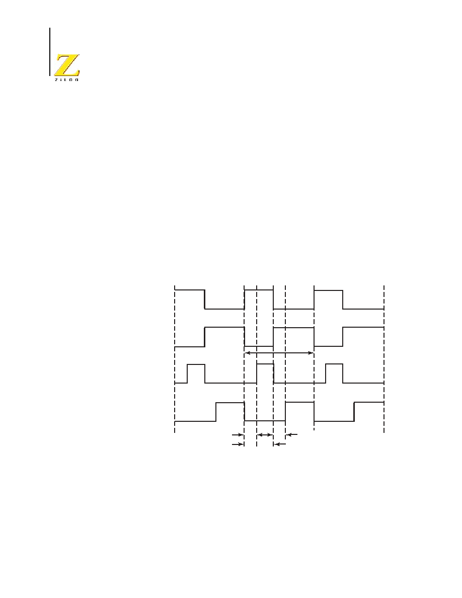
Pulse-Width Modulator
P R E L I M I N A R Y
PS024604-1005
Z8 Encore!
�
Motor Control Flash MCUs
Product Specification
70
PWM Prescaler
The prescaler allows the PWM clock signal to be decreased by factors of 1, 2, 4, or 8 with
respect to the system clock. The
PRES[1:0]
bit field in the PWM Control 1 Register
(PWMCTL1) controls prescaler operation. This 2-bit
PRES
field is buffered so that the
prescale value only changes upon a PWM reload event.
PWM Period and Count Resolution
The PWM counter operates in two modes to allow edge-aligned outputs and center-
aligned outputs. Figures 8 and 9 illustrate edge- and center-aligned PWM outputs. The
period of the PWM outputs, PERIOD, is determined by which mode the PWM counter is
operating. The active time of a PWM output is determined by the programmed duty cycle,
PWMDC, and the programmed deadband time, PWMDB.
The sections that follow these two figures describe the PWM timer modes and the regis-
ters that control the duty cycle and deadband time.
Figure 8. Edge-Aligned PWM Output
Period
PWMDB
PWMDC
PWMDB
PWMxH
No Deadband
PWMxH
Deadband Insertion
PWMxL
PWMxL

PS024604-1005
P R E L I M I N A R Y
PWM Period and Count Resolution
Z8FMC16100 Series Flash MCU
Product Specification
71
Edge-Aligned Mode
In Edge-Aligned PWM mode, a 12-bit up counter creates the PWM period with a mini-
mum resolution equal to the PWM clock source period. The counter counts up to the
reload value, resets to
000h
, and then resumes counting.
Center-Aligned Mode
In Center-Aligned PWM mode, a 12-bit up/down counter creates the PWM period with a
minimum resolution equal to twice the PWM clock source period. The counter counts up
to the reload value and then counts down to 0.
Figure 9. Center-Aligned PWM Output
Edge-Aligned PWM Mode Period =
Prescaler x (Reload Value +1)
f
SYSTEMCLK
Center-Aligned PWM Mode Period =
2 x Prescaler x (Reload Value +1)
f
SYSTEMCLK
Period
PWMDC
PWMDB
PWMDB
PWMxH
No Deadband
PWMxH
Deadband Insertion
PWMxL
PWMxL

Pulse-Width Modulator
P R E L I M I N A R Y
PS024604-1005
Z8 Encore!
�
Motor Control Flash MCUs
Product Specification
72
PWM Duty Cycle Registers
The PWM Duty Cycle registers (PWM0HD, PWM0LD, PWM1HD, PWM1LD,
PWM2HD, PWM2LD) contain a 16-bit signed value, in which bit 15 is the sign bit. The
Duty Cycle value is compared to the current 12-bit unsigned PWM count value. If the
PWM Duty Cycle value is set less than or equal to 0, the PWM output is deasserted for the
full PWM period. If the PWM Duty Cycle value is set to a value greater than the PWM
reload value, the PWM output is asserted for the full PWM period.
Independent and Complementary PWM Outputs
The six PWM outputs are configurable to operate independently, or as three complemen-
tary pairs. Operation as six independent PWM channels is enabled by setting the
INDEN
bit in the PWM Control 1 Register (PWMCTL1). The
PWEN
bit must be cleared to alter
this bit. In independent mode, each PWM output uses its own PWM duty cycle value.
When configured to operate as three complementary pairs, the PWM duty cycle values
PWM0HD, PWM1HD, and PWM2HD control the modulator output. In complementary
output mode, deadband time is also inserted.
The POLx bits in the PWM Control 1 Register (PWMCTL1) select the relative polarity of
the High and Low signals. As illustrated in
Figures 8 and 9
, when the POLx bits are
cleared to 0, the High PWM output will start in the ON state and transition to the OFF
state when the PWM timer count reaches the programmed duty cycle. The Low PWM
value starts in the OFF state and transitions to the ON state as the PWM timer count
reaches the value in the associated duty cycle register. Alternately, setting the POLx
causes the High output to start in the OFF state and the Low output to start in the ON state.
Manual Off-State Control of PWM Output Channels
Each PWM output can be controlled directly by the modulator logic or set to the OFF
state. To manually set the PWM outputs to the OFF state, set the
OUTCTL
bit and the asso-
ciated
OUTx
bits in the PWM Output Control Register (PWMOUT). OFF state control
operates individually by channel. For example, suppressing the single output of a pair
allows the complementary channel to continue operating. Similarly, if the outputs are
operating independently, disabling one output channel has no effect on the other PWM
outputs.
Deadband Insertion
When the PWM outputs are configured to operate as complementary pairs, an 8-bit dead-
band value can be defined in the PWM Deadband Register (PWMDB). Inserting deadband
time causes the modulator to separate the deassertion of one PWM signal from the asser-
tion of its complement. This separation is essential for many motor control applications in
that it prevents simultaneous turn-on of the High and Low drive transistors. The deadband

PS024604-1005
P R E L I M I N A R Y
Minimum PWM Pulse Width Filter
Z8FMC16100 Series Flash MCU
Product Specification
73
counter directly counts system clock cycles and is unaffected by PWM prescaler settings.
The width of this deadband is attributed to the number of system clock cycles specified in
the PWM Deadband Register (PWMDB). The minimum deadband duration is one system
clock, and the maximum duration is 255 system clocks. During the deadband period, both
PWM outputs of a complementary pair are deasserted. The generation of deadband time
does not alter the PWM period; instead, the deadband time is subtracted from the active
time of the PWM outputs.
Figures 8 and 9
show the effect of deadband insertion on the
PWM output.
Minimum PWM Pulse Width Filter
The PWM modulator is capable of producing pulses as narrow as a single system clock
cycle in width. Because the response time of external drive circuits may be slower than the
period of a system clock, a filter is implemented to enforce a minimum-width pulse on the
PWM output pins. All output pulses, whether High or Low, must be at least the minimum
number of PWM clock cycles (see the
PWM Prescaler
section on page 70 for more infor-
mation) in width as specified in the PWM Minimum Pulse Width Filter (PWMMPF) Reg-
ister. If the expected pulse width is less than the threshold, the associated PWM output
does not change state until the duty cycle value has changed sufficiently to allow pulse
generation of an acceptable width. The minimum pulse width filter also accounts for the
duty cycle variation caused by the deadband insertion. The PWM output pulse is filtered
even if the programmed duty cycle is greater than the threshold, but the pulse width
decrease because of deadband insertion causes the pulse to be too narrow. The pulse width
filter value is calculated as:
where
T
MINPULSEOUT
is the shortest allowed pulse width on the PWM outputs, in seconds.
The PWM Minimum Pulse Width Filter Register can only be written when the
PWEN
bit is
cleared. Values written to this register when
PWEN
is set will be ignored.
Synchronization of PWM and Analog-to-Digital Converter
The analog-to-digital converter (ADC) on the Z8FMC16100 Series Flash MCU can be
synchronized with the PWM period. Enabling the PWM ADC trigger causes the PWM to
generate an ADC conversion signal at the end of each PWM period. Additionally, in cen-
ter-aligned mode, the PWM will generate a trigger at the center of the period. Setting the
ADCTRIG bit in the PWM Control 0 Register (PWMCTL0) enables ADC synchroniza-
tion.
roundup(PWMMPF) =
T
MINPULSEOUT
T
SYSTEMCLOCK
x PWM
PRESCALER

Pulse-Width Modulator
P R E L I M I N A R Y
PS024604-1005
Z8 Encore!
�
Motor Control Flash MCUs
Product Specification
74
PWM Timer and Fault Interrupts
The PWM generates interrupts to the eZ8 CPU upon any of the following events:
PWM Reload.
The interrupt is generated at the end of a PWM period when a PWM regis-
ter reload occurs (the
READY
bit is set).
PWM Fault.
A fault condition is indicated by asserting any of the FAULT pins, or by the
assertion of the comparator.
Fault Detection and Protection
The Z8FMC16100 Series Flash MCU contains hardware and software fault controls that
allow rapid deassertion of all enabled PWM output signals. A logic Low on an external
fault pin (FAULT0 or FAULT1), or the assertion of the overcurrent comparator, forces the
PWM outputs to a predefined OFF state.
Similar deassertion of the PWM outputs can be accomplished in software by writing to the
PWMOFF
bit in the PWM Control 0 Register. The PWM counter continues to operate while
the outputs are deasserted (made inactive) due to one of these fault conditions.
The fault inputs can be individually enabled through the PWM Fault Control Register. If a
fault condition is detected and the source is enabled, a fault interrupt is generated. The
PWM Fault Status Register (PWMFSTAT) is read to determine which fault source has
caused the interrupt.
After a fault has been detected, and after the PWM outputs are disabled, modulator control
of the PWM outputs can be reenabled either by software, or by deassertion of the FAULT
input signal. Selection of either method is made via the PWM Fault Control Register
(PWMFCTL). Configuration of the fault modes and reenable methods allows pulse-by-
pulse limiting and hard shutdown. When configured in automatic restart mode, the PWM
outputs are reengaged at beginning of the next PWM cycle (the master timer value is equal
to 0) if all fault signals are deasserted. In a software-controlled restart, all fault inputs must
be deasserted and all fault flags cleared.
The fault input pin is Schmitt-triggered. The input signal from the pin, as well as the com-
parators, pass though an analog filter to reject high-frequency noise.
The logic path from the fault sources to the PWM outputs is asynchronous, which ensures
that the fault inputs will force the PWM outputs to their OFF state, even if the system
clock is stopped.
PWM Operation in CPU Halt Mode
When the eZ8 CPU is operating in HALT mode, the Pulse-Width Modulator continues to
operate, if enabled. To minimize the current in HALT mode, the Pulse-Width Modulator
must be disabled by clearing the
PWMEN
bit to 0.

PS024604-1005
P R E L I M I N A R Y
PWM Operation in CPU Stop Mode
Z8FMC16100 Series Flash MCU
Product Specification
75
PWM Operation in CPU Stop Mode
When the eZ8 CPU is operating in STOP mode, the Pulse-Width Modulator is disabled,
because the system clock ceases to operate in STOP mode. The PWM outputs remain in
the same state as they were prior to entering STOP mode. In normal operation, the PWM
outputs must be disabled by the software prior to the CPU entering STOP mode. A fault
condition detected in STOP mode forces the PWM outputs to a predefined OFF state.
Observing the State of PWM Output Channels
The logic value of the PWM outputs can be sampled by reading the PWMIN register. If a
PWM channel pair is disabled (an option bit is not set), the associated PWM outputs are
forced to high-impedance, and can be used as general-purpose inputs.
PWM High and Low Byte Registers
The PWM High and Low Byte (PWMH and PWML) registers, shown in Tables 42 and
43, contain the current 12-bit PWM count value. Reads from PWMH cause the value in
PWML to be stored in a temporary holding register. A read from PWML always returns
this temporary register value.
Writing to the PWM High and Low Byte registers while the PWM is enabled is not rec-
ommended. There are no temporary holding registers for Write operations, so simulta-
neous 12-bit Writes are not possible.
If either the PWM High or Low Byte registers are written during counting, the 8-bit writ-
ten value is placed in the counter (High or Low byte) at the next clock edge. The counter
continues counting from the new value.
Table 42. PWM High Byte Register (PWMH)
BITS
7
6
5
4
3
2
1
0
FIELD
Reserved
PWMH
RESET
0H
0H
R/W
R/W
R/W
ADDR
F2CH
Caution:

Pulse-Width Modulator
P R E L I M I N A R Y
PS024604-1005
Z8 Encore!
�
Motor Control Flash MCUs
Product Specification
76
PWMH and PWML--PWM High and Low Bytes
These 2 bytes, {PWMH[3:0], PWML[7:0]}, contain the current 12-bit PWM count value.
PWM Reload High and Low Byte Registers
The PWM Reload High and Low Byte (PWMRH and PWMRL) registers, shown in Table
44 and Table 45, store a 12-bit reload value, {PWMRH[3:0], PWMRL[7:0]}. The PWM
reload value is held in buffer registers. The PWM reload value written to the buffer regis-
ters is not used by the PWM generator until the next PWM reload event occurs. Reads
from these registers always return the values from the buffer registers.
Table 43. PWM Low Byte Register (PWML)
BITS
7
6
5
4
3
2
1
0
FIELD
PWML
RESET
00H
R/W
R/W
ADDR
F2DH
Edge-Aligned PWM Mode Period =
Prescaler x Reload Value
f
PWMCLK
Center-Aligned PWM Mode Period =
2 x Prescaler x Reload Value
f
PWMCLK
Table 44. PWM Reload High Byte Register (PWMRH)
BITS
7
6
5
4
3
2
1
0
FIELD
Reserved
PWMRH
RESET
0H
FH
R/W
R/W
R/W
ADDR
F2EH

PS024604-1005
P R E L I M I N A R Y
PWM 0�2 Duty Cycle High and Low Byte
Z8FMC16100 Series Flash MCU
Product Specification
77
PWMRH and PWMRL--PWM Reload Register High and Low
These two bytes form the 12-bit Reload value, {PWMRH[3:0], PWMRL[7:0]}. This value
sets the PWM period.
PWM 0�2 Duty Cycle High and Low Byte Registers
The PWM 0�2 H/L Duty Cycle High and Low Byte (PWMxDH and PWMxDL) registers,
shown in Table 46 and Table 47, set the duty cycle of the PWM signal. This 14-bit signed
value is compared to the PWM count value to determine the PWM output. Reads from
these registers always return the values from the temporary holding registers. The PWM
duty cycle value is not used by the PWM generator until the next PWM reload event
occurs.
Writing a negative value (DUTYH[7] = 1) forces the PWM to be OFF for the full PWM
period. Writing a positive value greater than the 12-bit PWM reload value forces the PWM
to be ON for the full PWM period.
Table 45. PWM Reload Low Byte Register (PWMRL)
BITS
7
6
5
4
3
2
1
0
FIELD
PWMRL
RESET
FF
R/W
R/W
ADDR
F2FH
PWM Duty Cycle =
PWM Duty Cycle Value
PWM Reload Value
Table 46. PWM 0-2 H/L Duty Cycle High Byte Register (PWMHxDH,PWMLxDH)
BITS
7
6
5
4
3
2
1
0
FIELD
SIGN
Reserved
DUTYH
RESET
0
00
0_0000
R/W
R/W
R/W
R/W
ADDR
F30H, F32H, F34H, F36H, F38H, F3AH

Pulse-Width Modulator
P R E L I M I N A R Y
PS024604-1005
Z8 Encore!
�
Motor Control Flash MCUs
Product Specification
78
PWM Control 0 Register
The PWM Control 0 (PWMCTL0) Register, shown in Table 48, controls PWM operation.
Table 47. PWM 0-2 H/L Duty Cycle Low Byte Register (PWMHxDL,PWMLxDL)
BITS
7
6
5
4
3
2
1
0
FIELD
DUTYL
RESET
00H
R/W
R/W
ADDR
F31H, F33H, F35H, F37H, F39H, F3BH
Bit
Position
Value
(H)
Description
[7]
SIGN
0
Duty Cycle Sign
Duty Cycle is a positive two's complement number.
1
Duty Cycle is a negative two's complement number. Output is forced to the off-
state.
[6:0], [7:0]
DUTYH and
DUTYL
PWM Duty Cycle High and Low Bytes
These two bytes, {DUTYH[7:0], DUTYL[7:0]}, form a 14-bit signed value (Bits 5
and 6 of the High Byte are always 0). The value is compared to the current 12-bit
PWM count.
Table 48. PWM Control 0 Register (PWMCTL0)
BITS
7
6
5
4
3
2
1
0
FIELD
PWMOFF
OUTCTL
ALIGN
Reserved ADCTRIG Reserved
READY
PWMEN
RESET
0
0
0
0
0
0
0
0
R/W
R/W
R/W
R/W
R/W
R/W
R/W
R/W
R/W
ADDR
F20H

PS024604-1005
P R E L I M I N A R Y
PWM Control 0 Register
Z8FMC16100 Series Flash MCU
Product Specification
79
Bit
Position
Value
(H)
Description
[7]
PWMOFF
0
Place PWM outputs in off-state
Disable modulator control of PWM pins. Outputs are in predefined off-state. This
is not dependent on the reload event.
1
Re-enable modulator control of PWM pins at next PWM reload event.
[6]
OUTCTL
0
PWM Output Control
PWM outputs are controlled by the Pulse-Width Modulator.
1
PWM outputs selectively disabled (set to off-state) according to values in the
OUTx bits of the PWMOUT register.
[5]
ALIGN
0
PWM Edge Alignment
PWM outputs are edge aligned.
1
PWM outputs are center aligned.
[4]
Reserved
Reserved
[3]
ADCTRIG
0
ADC Trigger Enable
No ADC trigger pulses.
1
ADC trigger enabled.
[2]
Reserved
0
Reserved
[1]
READY
0
Values Ready for Next Reload Event
PWM values (pre-scale, period, and duty cycle) are not ready. Do not use
values in holding registers at next PWM reload event
1
PWM values (pre-scale, period, and duty cycle) are ready. Transfer all values
from temporary holding registers to working registers at next PWM reload event.
[0]
PWMEN
0
PWM Enable
Pulse-width modulator is disabled and enabled PWM output pins are forced to
default off-state. PWM master counter is stopped. Certain control registers may
only written in this state.
1
Pulse-width modulator is enabled and PWM output pins are enabled as outputs.
Pulse-Width Modulator
P R E L I M I N A R Y
PS024604-1005
Z8 Encore!
�
Motor Control Flash MCUs
Product Specification
80
PWM Control 1 Register
The PWM Control 1 (PWMCTL1) Register, shown in Table 49, controls portions of PWM
operation.
Table 49. PWM Control 1 Register (PWMCTL1)
BITS
7
6
5
4
3
2
1
0
FIELD
RLFREQ[1:0]
INDEN
Pol45
Pol23
Pol10
PRES[1:0]
RESET
00
0
0
0
0
00
R/W
R/W
R/W
R/W
R/W
R/W
R/W
ADDR
F21H
Bit
Position
Value
(H)
Description
[7:6]
RLFREQ[1:0]
00
01
10
11
Reload Event Frequency
This bit field is buffered. Changes to the reload event frequency takes effect at
the end of the current PWM period. Reads always return the bit values from the
temporary holding register.
PWM reload event occurs at the end of every PWM period.
PWM reload event occurs once every 2 PWM periods.
PWM reload event occurs once every 4 PWM periods.
PWM reload event occurs once every 8 PWM periods.
[5]
INDEN
0
Independent PWM Mode Enable
This bit may only be altered when PWEN (PWMCTL0) cleared.
PWM outputs operate as 3 complementary pairs.
1
PWM outputs operate as 6 independent channels.
[4]
Pol2
1
Invert Ouput polarity for channel pair PWM2.
0
Non-inverted polarity for channel pair PWM2.
[3]
Pol1
1
Invert Ouput polarity for channel pair PWM1.
0
Non-inverted polarity for channel pair PWM1.
[2]
Pol0
1
Invert Ouput polarity for channel pair PWM0.
0
Non-inverted polarity for channel pair PWM0.

PS024604-1005
P R E L I M I N A R Y PWM
Deadband
Register
Z8FMC16100 Series Flash MCU
Product Specification
81
PWM Deadband Register
The PWM Deadband (PWMDB) Register, shown in Table 50, stores the 8-bit PWM dead-
band value. This register determines the number of system clock cycles inserted as dead-
time in complementary output mode. The minimum deadband value is 1.
[1:0]
PRES
00
01
10
11
PWM Prescaler
The prescaler divides down the PWM input clock (either the system clock or the
PWMIN external input). This field is buffered. Changes to this field take effect at
the next PWM reload event. Reads always return the values from the
temporary holding register.
Divide by 1
Divide by 2
Divide by 4
Divide by 8
Table 50. PWM Dead-Band Register (PWMDB)
BITS
7
6
5
4
3
2
1
0
FIELD
PWMDB[7:0]
RESET
01H
R/W
R/W
ADDR
F22H
Bit
Position
Value
(H)
Description
[7:0]
PWMDB
PWM Dead band
Sets the PWM dead band period for which both PWM outputs of a
complementary PWM output pair are deasserted.
Note: This register can only be written when PWEN is cleared.
Bit
Position
Value
(H)
Description
Pulse-Width Modulator
P R E L I M I N A R Y
PS024604-1005
Z8 Encore!
�
Motor Control Flash MCUs
Product Specification
82
PWM Minimum Pulse Width Filter
The value in the PWM Minimum Pulse Width Filter (PWMMPF) Register, shown in Table
51, determines the minimum width pulse, either high or low, that can be generated by the
PWM module. The minimum pulse width period is calculated as:
A Value other than 00H must be written to the PWMMPF registor or the PWM output
waveform will be distorted!
PWM Fault Mask Register
The PWM Fault Mask (PWMFM) Register, shown in Table 52, enables individual fault
sources. PWM behaviour when an input is asserted is determined by the PWM Fault Con-
trol Register (PWMFCTL).
T
MINPULSEOUT
=
PWMDB + PWMMPF
T
SYSTEMCLOCK
x PWMPrescale
Table 51. PWM Minimum Pulse Width Filter (PWMMPF)
BITS
7
6
5
4
3
2
1
0
FIELD
PWMMPF[7:0]
RESET
00H
R/W
R/W
ADDR
F23H
Bit
Position
Value
(H)
Description
[7:0]
PWMMPF
PWM Minimum Pulse Filter
Sets the minimum allowed output pulse width in PWM clock cycles.
Note: This register can only be written when PWEN is cleared.
Table 52. PWM Fault Mask Register (PWMFM)
BITS
7
6
5
4
3
2
1
0
FIELD
Reserved
DBGMSK
Reserved
F1MASK
C0MASK
FMASK
RESET
00
0
000
0
0
0
R/W
R
R/W
R
R/W
R/W
R/W
ADDR
F24H
Caution:

PS024604-1005
P R E L I M I N A R Y
PWM Fault Status Register
Z8FMC16100 Series Flash MCU
Product Specification
83
PWM Fault Status Register
The PWM Fault Status (PWMFSTA) Register, shown in Table 53, provides status of fault
inputs and timer reload.. The fault flags indicate which fault source is active. If a fault
source is masked the flag in this register will not be set if the source is asserted. The
reload flag is set when the timer compare vaules are updated. Clear flags by writing a 1 to
the flag bits. Fault flag bits can only be cleared if the associated fault source has deas-
serted.
Bit
Position
Value
(H)
Description
[7:6]
Reserved
Must be 0.
[5]
DBGMSK
0
Debug Entry Fault Mask
Entering CPU DEBUG Mode generates a PWM fault.
1
Entering CPU DEBUG mode does not generate a PWM fault.
[4:3]
Reserved
Must be 0.
[2]
F1MASK
0
Fault 1 Fault Mask
Fault 1 generates a PWM fault.
1
Fault 1 does not generate a PWM fault.
[1]
C0MASK
0
Comparator Fault Mask
Comparator generates a PWM fault.
1
Comparator does not generate a PWM fault.
[0]
F0MASK
0
Fault Pin Mask
Fault0 pin generates a PWM fault.
1
Fault0 pin does not generate a PWM fault.
Note: This register can only be written when PWEN is cleared.

Pulse-Width Modulator
P R E L I M I N A R Y
PS024604-1005
Z8 Encore!
�
Motor Control Flash MCUs
Product Specification
84
Table 53. PWM Fault Status Register (PWMFSTAT)
BITS
7
6
5
4
3
2
1
0
FIELD
RLDFlag Reserved
DBGFLAG
Reserved
F1FLAG
C0FLAG
FFLAG
RESET
U
0
U
00
U
U
U
R/W
R/W1C
R
R/W1C
R
R/W1C
R/W1C
R/W1C
ADDR
F25H
Bit
Position
Value
(H)
Description
[7]
RLDFlag
Reload Flag
This bit is set and latched when a PWM timer reload occurs. Writing a 1 to this bit
clears the flag.
[6]
Reserved
0
Reserved
Always reads 0.
[5]
DBGFLAG
Debug Flag
This bit is set and latched when DEBUG mode is entered. Writing a 1 to this bit
clears the flag.
[4:3]
Reserved
0
Reserved
Always reads 0.
[2]
F1FLAG
Fault1
Flag
This bit is set and latched when Fault1 is asserted. Writing a 1 to this bit clears
the flag.
[1]
C0FLAG
Comparator 0 Flag
This bit is set and latched when Comparator is asserted. Writing a 1 to this bit
clears the flag.
[0]
FFLAG
Fault
Flag
This bit is set and latched when the FAULT0 input is asserted. Writing a 1 to this
bit clears the flag.
Note: For this register, W1C means you must write one to clear the flag.

PS024604-1005
P R E L I M I N A R Y
PWM Fault Control Register
Z8FMC16100 Series Flash MCU
Product Specification
85
PWM Fault Control Register
The PWM Fault Control (PWMFCTL) Register, shown in Table 54, determines how the
PWM recovers from a fault condition. Settings in this register select automatic or software
controlled PWM restart.
Table 54. PWM Fault Control Register (PWMFCTL)
BITS
7
6
5
4
3
2
1
0
FIELD
Reserved DBGRST Fault1INT Fault1RST CMPINT
CMPRST Fault0INT Fault0RST
RESET
0
0
0
0
0
0
0
0
R/W
R/W
R/W
R/W
R/W
R/W
R/W
R/W
R/W
ADDR
F28H
Bit
Position
Value
(H)
Description
[7]
Reserved
0
Reserved.
[6]
DBGRST
0
DebugRestart
Automatic recovery. PWM resumes control of outputs when all fault sources have
deasstered and a new PWM period begins.
1
S
oftware controlled recovery. PWM resumes control of outputs only after all fault
sources have deasserted and all fault flags are cleared and a PWM reload occurs
[5]
Fault1INT
0
Fault 1 Interrupt
Interrupt on comparator assertion disabled.
1
Interrupt on comparator assertion enabled.
[4]
Fault1RST
0
Fault 1 Restart
Automatic recovery. PWM resumes control of outputs when all fault sources have
deasstered.
1
S
oftware controlled recovery. PWM resumes control of outputs only after all fault
sources have deasserted and all fault flags are cleared and a PWM reload occurs
[3
CMP0INT
0
Comparator 0 Interrupt
Interrupt on comparator 0 assertion disabled.
1
Interrupt on comparator 0 assertion enabled.
[2]
CMP0RST
0
Comparator 0 Restart
Automatic recovery. PWM resumes control of outputs when all fault sources have
deasstered.
1
S
oftware controlled recovery. PWM resumes control of outputs only after all fault
sources have deasserted and all fault flags are cleared and a PWM reload occurs
Pulse-Width Modulator
P R E L I M I N A R Y
PS024604-1005
Z8 Encore!
�
Motor Control Flash MCUs
Product Specification
86
PWM Input Sample Register
PWM pin values are sampled by reading the PWM Input Sample Register, shown in Table
55.
[1]
Fault0INT
0
Fault 0 Interrupt
Interrupt on Fault0 pin assertion disabled.
1
Interrupt on Fault0 pin assertion enabled.
[0]
Fault0RST
0
Fault 0 Restart
Automatic recovery. PWM resumes control of outputs when all fault sources have
deasstered.
1
S
oftware controlled recovery. PWM resumes control of outputs only after all fault
sources have deasserted and all fault flags are cleared and a PWM reload occurs
Note: This register can only be written when PWEN is cleared.
Table 55. PWM Input Sample Register (PWMIN)
BITS
7
6
5
4
3
2
1
0
FIELD
Reserved
FAULT
IN2L
IN2H
IN1L
IN1H
IN0L
IN0H
RESET
0
0
0
0
0
0
0
0
R/W
R
R/W
R/W
R/W
R/W
R/W
R/W
R/W
ADDR
F26H
Bit
Position
Value
(H)
Description
[7]
Reserved
Must be 0.
[6]
FAULT
0
Sample Fault0 pin
A Low level signal was read on the FAULT pin.
1
A High level signal was read on the FAULT pin.
[5:0]
IN2L/IN2H/
IN1L/IN1H/
IN0L/IN0H
0
Sample PWM pins
A Low level signal was read on the pins.
1
A High level signal was read on the pins.
Bit
Position
Value
(H)
Description

PS024604-1005
P R E L I M I N A R Y
PWM Output Control Register
Z8FMC16100 Series Flash MCU
Product Specification
87
PWM Output Control Register
The PWM Output Control (PWMOUT) Register, shown in Table 56, enables modulator
control of the six PWM output signals. Output control is enabled by the OUTCTL bit in
the PWMCTL0 register. The Pulse-Width Modulator continues to operate, but has no
effect on the disabled PWM pins. If a fault condition is detected all PWM outputs are
forced to their selected OFF state.
.
Current Sense ADC Trigger Control Register
An ADC trigger is generated when the PWM output signals match the state specified by
the Current-Sense ADC-Trigger control register. The match logic is an AND-OR tree that
will solve to true if based on the register settings. An ADC conversion will be triggered on
the rising edge of this signal. The logic equation for the adc-trigger is:
ADCTRIGGER = CSTPOL ^ (
( HEN & PWM0H &PWM1H & PWM2H) |
( LEN & PWM0L &PWM1L & PWM2L) |
( nHEN & !PWM0H &!PWM1H & !PWM2H) |
( nLEN & !PWM0H & !PWM1H & !PWM2H) )
Table 56. PWM Output Control Register (PWMOUT)
BITS
7
6
5
4
3
2
1
0
FIELD
Reserved Reserved
OUT2L
OUT2H
OUT1L
OUT1H
OUT0L
OUT0H
RESET
0
0
0
0
0
0
0
0
R/W
R
R
R/W
R/W
R/W
R/W
R/W
R/W
ADDR
F27H
Bit
Position
Value
(H)
Description
[7,6]
Reserved
Must be 0.
[5, 3, 1]
OUT2L/
OUT1L/
OUT0L
0
PWM 2L/1L/0L Output Configuration
PWM 2L/1L/0L output signal is enabled and controlled by PWM.
1
PWM
2L/1L/0L
output signal is in low-side off-state.
[4, 2, 0]
OUT2H/
OUT1H/
OUT0H
0
PWM 2H/1H/0H Output Configuration
PWM 2H/1H/0H output signal is enabled and controlled by PWM.
1
PWM 2H/1H/0H output signal is in high-side off-state.

Pulse-Width Modulator
P R E L I M I N A R Y
PS024604-1005
Z8 Encore!
�
Motor Control Flash MCUs
Product Specification
88
where
�
the ^ symbol indicates a logical exclusive OR (XOR) function
�
the & symbol indicates a logical AND function
�
the | symbol indicates a logical OR function
�
the ! symbol indicates a logical NOT function
The combinations of polarity, enable, and PWM signals allow the logic to generate a
ADC-trigger under a wide variety of operating conditions. The HEN, LEN, nHEN, and
nLEN bits enable a group in the or logic. The CSTWMx bits allow the level of the PWM
output signals to control the equation. If a CSTPWMx bit is cleared, the value of the asso-
ciated PWMx output will always evaluate to a TRUE condition in the equation. Note that
these bits DO NOT affect the actual PWM outputs.
.
Table 57. Current-Sense Trigger Control Register (PWMSHC)
BITS
7
6
5
4
3
2
1
0
FIELD
CSTPOL
HEN
NHEN
LEN
NLEN
CSTPWM2 CSTPWM1 CSTPWM0
RESET
0
0
0
0
0
0
0
0
R/W
R/W
R/W
R/W
R/W
R/W
R/W
R/W
R/W
ADDR
F29H
Bit
Position
Value
(H)
Description
[7]
CSTPOL
0
Sample Hold Polarity
Hold when terms are active
1
Hold when terms are not active
[6]
HEN
0
High Side Active enable
Ignore Product of PWM0H, PWM1H, PWM2H in Sample/Hold equation
1
Hold when PWM0H, PWM1H, PWM2H are all active
[5]
NHEN
0
High Side inactive enable
Ignore Product of
PWM0H
,
PWM1H
,
PWM2H
in Sample/Hold equation
1
Hold when are all active
[4]
LEN
0
Low Side Active enable
Ignore Product of PWM0L, PWM1L, PWM2L in Sample/Hold equation
1
Hold when PWM0L, PWM1L, PWM2L are all active

PS024604-1005
P R E L I M I N A R Y Current
Sense ADC Trigger Control Register
Z8FMC16100 Series Flash MCU
Product Specification
89
[3]
NLEN
0
Low Side Inactive enable
Ignore Product of
PWM0L, PWM1L, PWM2L
in Sample/Hold equation
1
Hold when
PWM0L, PWM1L, PWM2L
are all active
[2]
CSTPWM2
0
PWM Channel2 Sample/Hold Enable
Channel 2 terms are not used in Sample/Hold Equation
1
Channel 2 terms are used in Sample/Hold Equation
[1]
CSTPWM1
0
PWM Channel1 Sample/Hold Enable
Channel 1 terms are not used in Sample/Hold Equation
1
Channel 1 terms are used in Sample/Hold Equation
[0]
CSTPWM0
0
PWM Channel0 Sample/Hold Enable
Channel 0 terms are not used in Sample/Hold Equation
1
Channel 0 terms are used in Sample/Hold Equation
Bit
Position
Value
(H)
Description

Pulse-Width Modulator
P R E L I M I N A R Y
PS024604-1005
Z8 Encore!
�
Motor Control Flash MCUs
Product Specification
90

PS024604-1005
P R E L I M I N A R Y Features
Z8FMC16100 Series Flash MCU
Product Specification
91
General-Purpose Timer
The Z8FMC16100 Series Flash MCU contains one 16-bit reloadable timer that can be
used for timing, event counting, or generation of pulse-width modulated (PWM) signals.
Features
�
16-bit reload counter
�
Programmable prescaler with prescale values from 1 to 128
�
PWM output generation (single or differential)
�
Capture and compare capability
�
External input pin for event counting, clock gating, or capture signal
�
Complementary Timer Output pins
�
Timer interrupt
Architecture
Capture and compare capability measures the velocity from a tachometer wheel or reads
sensor outputs for rotor position for brushless DC motor commutation. Figure 10 illus-
trates the architecture of the timer.
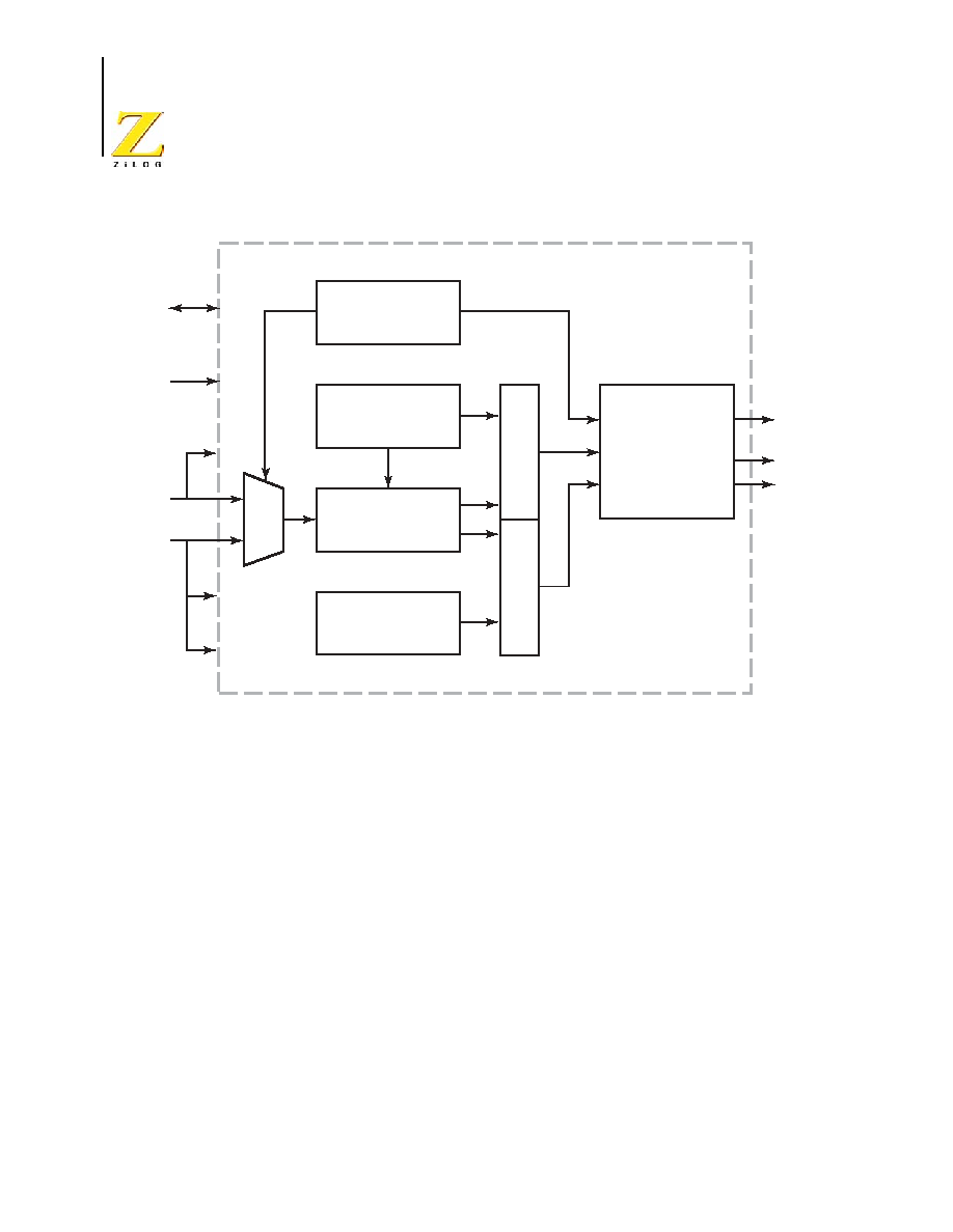
General-Purpose Timer
P R E L I M I N A R Y
PS024604-1005
Z8 Encore!
�
Motor Control Flash MCUs
Product Specification
92
Operation
The general-purpose timer is a 16-bit up-counter. In normal operation, the timer is initial-
ized to
0001h
. After it is enabled, the timer counts up to the value contained in the Reload
High and Low Byte registers, then resets to
0001h
. The counter either halts or continues,
depending on its current mode of operation.
Minimum time-out delay (1 system clock in duration) is set by loading the value
0001h
into the Timer Reload High and Low Byte registers and setting the prescale value to 1.
Maximum time-out delay (2
16
x 2
7
system clocks) is set by loading the value
0000h
into
the Timer Reload High and Low Byte registers and setting the prescale value to 128.
When the timer reaches
FFFFh
, the timer rolls over to
0000h
.
If the reload register is set to a value less than the current counter value, the counter con-
tinues counting until reaching
FFFFh
, rolls over to
0000h
, and continues counting until
reaching the reload value, then resets to
0001h
.
Figure 10. Timer Block Diagram
Data
Bus
Block
Control
System
Clock
Timer
Input
Gate Input
Capture Input
Timer
Interrupt
Interrupt,
PWM, and
Timer Output
Control
Timer Control
16-Bit
Reload Register
16-Bit Counter
with Prescaler
16-Bit
PWM/Compare
T
OUT
T
OUT
Timer Block
Compare
Compare

PS024604-1005
P R E L I M I N A R Y Timer
Operating
Modes
Z8FMC16100 Series Flash MCU
Product Specification
93
Timer Operating Modes
The timers can be configured to operate in the following eleven modes, each of which is
described in this section:
�
ONE-SHOT mode
�
TRIGGERED ONE-SHOT mode
�
CONTINUOUS mode
�
COUNTER mode
�
COMPARATOR COUNTER mode
�
PWM SINGLE OUTPUT mode
�
PWM DUAL OUTPUT mode
�
CAPTURE RESTART mode
�
CAPTURE COMPARE mode
�
COMPARE mode
�
GATED mode
One-Shot Mode
In ONE-SHOT mode, the timer counts up to the 16-bit reload value stored in the Timer
Reload High and Low Byte registers. The Timer Input is the system clock. After reaching
this reload value, the timer generates an interrupt and the count value in the Timer High
and Low Byte registers is reset to
0001h
. The timer is automatically disabled and stops
counting.
If the Timer Output alternate function is enabled, the Timer Output pin changes state for
one system clock cycle (from Low to High, then back to Low if
TPOL
= 0) at timer reload.
If the user chooses, the Timer Output can undergo a permanent state change upon One-
Shot time-out, as follows:
1. Set the
TPOL
bit in the Timer Control 1 Register to the start value before beginning
ONE-SHOT mode.
2. After starting the timer, set
TPOL
to the opposite value.
The steps for configuring a timer for ONE-SHOT mode and initiating a count are as fol-
lows:
1. Write to the Timer Control registers to:
a. Disable the timer.
b. Configure the timer for ONE-SHOT mode.
c. Set the prescale value.

General-Purpose Timer
P R E L I M I N A R Y
PS024604-1005
Z8 Encore!
�
Motor Control Flash MCUs
Product Specification
94
d. If using the Timer Output alternate function, set the initial output level (High or
Low) using the
TPOL
bit.
e. Set the interrupt mode.
2. Write to the Timer High and Low Byte registers to set the starting count value.
3. Write to the Timer Reload High and Low Byte registers to set the reload value.
4. If appropriate, enable the timer interrupt and set the timer interrupt priority by writing
to the relevant interrupt registers.
5. If using the Timer Output function, configure the associated GPIO port pin for the
Timer Output alternate function.
6. Write to the Timer Control 1 Register to enable the timer and initiate counting.
The timer period is calculated by the following equation (Start Value is typically = 1):
Triggered One-Shot Mode
In TRIGGERED ONE-SHOT mode, the timer operates as follows:
1. The Timer idles until a trigger is received. The timer trigger is taken from the Timer
Input pin. The
TPOL
bit in the Timer Control 1 Register selects whether the trigger
occurs on the rising edge or the falling edge of the Timer Input signal.
2. Following the trigger event, the timer counts system clocks up to the 16-bit reload
value stored in the Timer Reload High and Low Byte registers.
3. Upon reaching the reload value, the timer outputs a pulse on the Timer Output pin,
generates an interrupt, and resets the count value in the Timer High and Low Byte reg-
isters to
0001h
. The duration of the output pulse is a single system clock. The
TPOL
bit also sets the polarity of the output pulse.
4. The timer idles until the next trigger event. Trigger events that occur while the timer is
responding to a previous trigger are ignored.
The steps for configuring Timer 0 in TRIGGERED ONE-SHOT mode and initiating oper-
ation are as follows:
1. Write to the Timer Control registers to:
a. Disable the timer.
b. Configure the timer for TRIGGERED ONE-SHOT mode.
One-Shot Mode Time-Out Period(s) =
(Reload Value � Start Value + 1) x Prescaler
System Clock Frequency (Hz)

PS024604-1005
P R E L I M I N A R Y Timer
Operating
Modes
Z8FMC16100 Series Flash MCU
Product Specification
95
c. Set the prescale value.
d. If using the Timer Output alternate function, set the initial output level (High or
Low) via the
TPOL
bit.
e. Set the INTERRUPT mode.
2. Write to the Timer High and Low Byte registers to set the starting count value.
3. Write to the Timer Reload High and Low Byte registers to set the reload value.
4. If appropriate, enable the timer interrupt and set the timer interrupt priority by writing
to the relevant interrupt registers.
5. If using the Timer Output function, configure the associated GPIO port pin for the
Timer Output alternate function.
6. Write to the Timer Control 1 Register to enable the timer. Counting does not start until
the appropriate input transition occurs.
The timer period is calculated by the following equation (Start Value is typically = 1):
The one-shot delay from input trigger to output includes the above-defined time-out
period, plus an additional delay of 2�3 system clock cycles, due to the synchronization of
the input trigger.
Continuous Mode
In CONTINUOUS mode, the timer counts up to the 16-bit reload value stored in the Timer
Reload High and Low Byte registers. After reaching the reload value, the timer generates
an interrupt, the count value in the Timer High and Low Byte registers is reset to
0001h
,
and counting resumes. Also, if the Timer Output alternate function is enabled, the Timer
Output pin changes state (from Low to High or from High to Low) after timer reload.
The steps for configuring a timer for CONTINUOUS mode and initiating the count are as
follows:
1. Write to the Timer Control registers to:
a. Disable the timer.
b. Configure the timer for CONTINUOUS mode.
c. Set the prescale value.
Triggered One-Shot Mode Time-Out Period(s) =
(Reload Value � Start Value + 1) x Prescaler
System Clock Frequency (Hz)
Note:

General-Purpose Timer
P R E L I M I N A R Y
PS024604-1005
Z8 Encore!
�
Motor Control Flash MCUs
Product Specification
96
d. If using the Timer Output alternate function, set the initial output level (High or
Low) via
TPOL
.
2. Write to the Timer High and Low Byte registers to set the starting count value (usually
0001h
). This setting only affects the first pass in CONTINUOUS mode. After the first
timer reload in CONTINUOUS mode, counting begins at the reset value of
0001h
.
3. Write to the Timer Reload High and Low Byte registers to set the reload period.
4. If appropriate, enable the timer interrupt and set the timer interrupt priority by writing
to the relevant interrupt registers.
5. If using the Timer Output function, configure the associated GPIO port pin for the
Timer Output alternate function.
6. Write to the Timer Control 1 Register to enable the timer and initiate counting.
The timer period is calculated by the following equation:
If an initial starting value other than
0001h
is loaded into the Timer High and Low Byte
registers, use the ONE-SHOT mode equation to determine the first time-out period.
Counter and Comparator Counter Modes
In COUNTER mode, the timer counts input transitions from a GPIO port pin. The Timer
Input is taken from the associated GPIO port pin. The
TPOL
bit in the Timer Control 1
Register selects whether the count occurs on the rising edge or the falling edge of the
Timer Input signal. In COUNTER mode, the prescaler is disabled.
The input frequency of the Timer Input signal must not exceed one-fourth the system
clock frequency.
In COMPARATOR COUNTER mode, the timer counts output transitions from an analog
comparator output. Timer 0 takes its input from the output of the comparator. The
TPOL
bit
in the Timer Control 1 Register selects whether the count occurs on the rising edge or the
falling edge of the comparator output signal. In COMPARATOR COUNTER mode, the
prescaler is disabled.
The frequency of the comparator output signal must not exceed one-fourth the system
clock frequency.
Continuous Mode Time-Out Period(s) =
Reload Value x Prescaler
System Clock Frequency (Hz)
Caution:
Caution:

PS024604-1005
P R E L I M I N A R Y Timer
Operating
Modes
Z8FMC16100 Series Flash MCU
Product Specification
97
After reaching the reload value stored in the Timer Reload High and Low Byte registers,
the timer generates an interrupt, the count value in the Timer High and Low Byte registers
is reset to
0001h
, and counting resumes.
If the Timer Output alternate function is enabled, the Timer Output pin changes state
(from Low to High or from High to Low) at timer reload.
The steps for configuring a timer for COUNTER and COMPARATOR COUNTER modes
and initiating the count are as follows:
1. Write to the Timer Control registers to:
a. Disable the timer.
b. Configure the timer for COUNTER or COMPARATOR COUNTER mode.
c. Select either the rising edge or falling edge of the Timer Input or comparator out-
put signal for the count. This choice also sets the initial logic level (High or Low)
for the Timer Output alternate function. However, the Timer Output function does
not have to be enabled.
2. Write to the Timer High and Low Byte registers to set the starting count value. This
setting only affects the first pass in the counter modes. After the first timer reload,
counting begins at the reset value of
0001h
.
3. Write to the Timer Reload High and Low Byte registers to set the reload value.
4. If appropriate, enable the timer interrupt and set the timer interrupt priority by writing
to the relevant interrupt registers.
5. Configure the associated GPIO port pin for the Timer Input alternate function
(COUNTER mode).
6. If using the Timer Output function, configure the associated GPIO port pin for the
Timer Output alternate function.
7. Write to the Timer Control 1 Register to enable the timer.
PWM Single and Dual Output Modes
In PWM SINGLE OUTPUT mode, the timer outputs a Pulse-Width Modulator (PWM)
output signal through a GPIO port pin. In PWM DUAL OUTPUT mode, the timer outputs
a Pulse-Width Modulator (PWM) output signal and also its complement through two
GPIO port pins. The timer first counts up to the 16-bit PWM match value stored in the
Timer PWM High and Low Byte registers. When the timer count value matches the PWM
value, the Timer Output toggles. The timer continues counting until it reaches the reload
value stored in the Timer Reload High and Low Byte registers. Upon reaching the reload
value, the timer generates an interrupt, the count value in the Timer High and Low Byte
registers is reset to
0001h
, and counting resumes.

General-Purpose Timer
P R E L I M I N A R Y
PS024604-1005
Z8 Encore!
�
Motor Control Flash MCUs
Product Specification
98
The Timer Output signal begins with a value equal to
TPOL
and then transitions to
TPOL
when the timer value matches the PWM value. The Timer Output signal returns to
TPOL
after the timer reaches the reload value, and is reset to
0001h
.
In PWM DUAL OUTPUT mode, the timer also generates a second PWM output signal,
Timer Output Complement (T
OUT
). A programmable deadband can be configured (
PWMD
field) to delay (0�128 system clock cycles) the Low to a High (inactive to active) output
transitions on these two pins. This configuration ensures a time gap between the deasser-
tion of one PWM output to the assertion of its complement.
The steps for configuring a timer for either PWM SINGLE or DUAL OUTPUT mode and
initiating PWM operation are as follows:
1. Write to the Timer Control registers to:
a. Disable the timer.
b. Configure the timer for the selected PWM mode.
c. Set the prescale value.
d. Set the initial logic level (High or Low) and PWM High/Low transition for the
Timer Output alternate function with the
TPOL
bit.
e. Set the deadband delay (DUAL OUTPUT mode) with the
PWMD
field.
2. Write to the Timer High and Low Byte registers to set the starting count value (typi-
cally
0001h
). The starting count value only affects the first pass in PWM mode. After
the first timer reset in PWM mode, counting begins at the reset value of
0001h
.
3. Write to the PWM High and Low Byte registers to set the PWM value.
4. Write to the Timer Reload High and Low Byte registers to set the reload value (PWM
period). The reload value must be greater than the PWM value.
5. If appropriate, enable the timer interrupt and set the timer interrupt priority by writing
to the relevant interrupt registers.
6. Configure the associated GPIO port pin(s) for the Timer Output alternate function.
7. Write to the Timer Control 1 Register to enable the timer and initiate counting.
The PWM period is determined by the following equation:
If an initial starting value other than
0001h
is loaded into the Timer High and Low Byte
registers, use the ONE-SHOT mode equation to determine the first PWM time-out period.
PWM Period(s) =
Reload Value x Prescaler
System Clock Frequency (Hz)

PS024604-1005
P R E L I M I N A R Y Timer
Operating
Modes
Z8FMC16100 Series Flash MCU
Product Specification
99
If
TPOL
is set to 0, the ratio of the PWM output High time to the total period is determined
by the equation:
If
TPOL
is set to 1, the ratio of the PWM output High time to the total period is determined
by the equation:
Capture Modes
There are three capture modes that provide slightly different methods for recording the
time of, or time interval between, Timer Input events. These modes are CAPTURE mode,
CAPTURE RESTART mode, and CAPTURE COMPARE mode. In all three modes, when
the appropriate Timer Input transition (capture event) occurs, the timer counter value is
captured and stored in the PWM High and Low Byte registers. The
TPOL
bit in the Timer
Control 1 Register determines whether the Capture occurs on a rising edge or a falling
edge of the Timer Input signal. The
TICONFIG
bit determines whether interrupts are gen-
erated on capture events, reload events, or both. The
INCAP
bit in Timer Control 0 Regis-
ter clears to indicate an interrupt caused by a reload event and sets to indicate the timer
interrupt is caused by an input capture event.
There is a delay from the input event to the timer capture of 2�3 system clock cycles, due
to internal synchronization logic.
If the Timer Output alternate function is enabled, the Timer Output pin changes state
(from Low to High or from High to Low) at timer reload. The initial value is determined
by the
TPOL
bit.
Capture Mode.
In CAPTURE mode, and after it is enabled, the timer counts continuously
and rolls over from
FFFFh
to
0000h
. When the capture event occurs, the timer counter
value is captured and stored in the PWM High and Low Byte registers, an interrupt is gen-
erated, and the timer continues counting. The timer continues counting up to the 16-bit
reload value stored in the Timer Reload High and Low Byte registers. Upon reaching the
reload value, the timer generates an interrupt and continues counting.
Capture Restart Mode.
In CAPTURE RESTART mode, after it is enabled, the timer
counts continuously until either the capture event occurs or the timer count reaches the 16-
bit compare value stored in the Timer Reload High and Low Byte registers. If the capture
event occurs first, the timer counter value is captured and stored in the PWM High and
Low Byte registers, an interrupt is generated, the count value in the Timer High and Low
Byte registers is reset to
0001h
, and counting resumes. If no capture event occurs, upon
PWM Output High Time Ratio (%) =
Reload Value � PWM Value
x 100
Reload Value
PWM Output High Time Ratio (%) =
PWM Value
x 100
Reload Value

General-Purpose Timer
P R E L I M I N A R Y
PS024604-1005
Z8 Encore!
�
Motor Control Flash MCUs
Product Specification
100
reaching the reload value, the timer generates an interrupt, the count value in the Timer
High and Low Byte registers is reset to
0001h
, and counting resumes.
Capture/Compare Mode.
CAPTURE/COMPARE mode is identical to CAPTURE
RESTART mode, except that counting does not start until the first external Timer Input
transition occurs. Every subsequent transition (after the first) of the Timer Input signal
captures the current count value. When the capture event occurs, an interrupt is generated,
the count value in the Timer High and Low Byte registers is reset to
0001h
, and counting
resumes. If no capture event occurs, upon reaching the compare value, the timer generates
an interrupt, the count value in the Timer High and Low Byte registers is reset to
0001h
,
and counting resumes.
The steps for configuring a timer for one of these capture modes and initiating the count
are as follows:
1. Write to the Timer Control registers to:
a. Disable the timer.
b. Configure the timer for the selected capture mode.
c. Set the prescale value.
d. Set the capture edge (rising or falling) for the Timer Input.
e. Configure the timer interrupt to be generated at the input capture event, the reload
event, or both, by setting the
TICONFIG
field.
2. Write to the Timer High and Low Byte registers to set the starting count value (typi-
cally
0001h
).
3. Write to the Timer Reload High and Low Byte registers to set the reload value.
4. If appropriate, enable the timer interrupt and set the timer interrupt priority by writing
to the relevant interrupt registers.
5. Configure the associated GPIO port pin for the Timer Input alternate function.
6. Write to the Timer Control 1 Register to enable the timer. In CAPTURE and CAP-
TURE RESTART modes, the timer begins counting. In CAPTURE COMPARE
mode, the timer does not start counting until the first input transition occurs.
In capture modes, the elapsed time from a timer start to a capture event can be calculated
using the following equation (Start Value is typically = 1):
Capture Elapsed Time (s) =
(Capture Value � Start Value +1) x Prescale
System Clock Frequency (Hz)

PS024604-1005
P R E L I M I N A R Y Timer
Operating
Modes
Z8FMC16100 Series Flash MCU
Product Specification
101
Compare Mode
In COMPARE mode, the timer counts up to the 16-bit compare value stored in the Timer
Reload High and Low Byte registers. After reaching the compare value, the timer gener-
ates an interrupt and counting continues (the timer value is not reset to
0001h
). If the
Timer Output alternate function is enabled, the Timer Output pin changes state (from Low
to High or from High to Low).
If the timer reaches
FFFFh
, the timer rolls over to
0000h
and continues counting.
The steps for configuring a timer for COMPARE mode and initiating the count are as fol-
lows:
1. Write to the Timer Control registers to:
a. Disable the timer.
b. Configure the timer for COMPARE mode.
c. Set the prescale value.
d. Set the initial logic level (High or Low) for the Timer Output alternate function, if
appropriate.
2. Write to the Timer High and Low Byte registers to set the starting count value.
3. Write to the Timer Reload High and Low Byte registers to set the Compare value.
4. If appropriate, enable the timer interrupt and set the timer interrupt priority by writing
to the relevant interrupt registers.
5. If using the Timer Output function, configure the associated GPIO port pin for the
Timer Output alternate function.
6. Write to the Timer Control 1 Register to enable the timer and initiate counting.
The compare time is calculated by the following equation (Start Value is typically = 1):
Gated Mode
In GATED mode, the timer counts only when the Timer Input signal is in its active state,
as determined by the
TPOL
bit in the Timer Control 1 Register. When the Timer Input sig-
nal is active, counting begins. A timer interrupt is generated when the Timer Input signal
transitions from active to inactive state, a timer reload occurs, or both, depending on
TICONFIG[1:0]
. To determine if a Timer Input signal deassertion generated the inter-
rupt, read the associated GPIO input value and compare it to the value stored in the
TPOL
bit.
Compare Mode Time (s) =
(Compare Value � Start Value +1) x Prescale
System Clock Frequency (Hz)

General-Purpose Timer
P R E L I M I N A R Y
PS024604-1005
Z8 Encore!
�
Motor Control Flash MCUs
Product Specification
102
The timer counts up to the 16-bit reload value stored in the Timer Reload High and Low
Byte registers. When reaching the reload value, the timer generates an interrupt, the count
value in the Timer High and Low Byte registers is reset to
0001h
, and counting continues
as long as the Timer Input signal is active. Also, if the Timer Output alternate function is
enabled, the Timer Output pin changes state (from Low to High or from High to Low) at
timer reload.
The steps for configuring a timer for GATED mode and initiating the count are as follows:
1. Write to the Timer Control registers to:
a. Disable the timer.
b. Configure the timer for GATED mode.
c. Set the prescale value.
d. Select the active state of the Timer Input via the
TPOL
bit.
2. Write to the Timer High and Low Byte registers to set the starting count value. This
setting only affects the first pass in GATED mode. After the first timer reset in
GATED mode, counting begins at the reset value of
0001h
.
3. Write to the Timer Reload High and Low Byte registers to set the reload value.
4. If appropriate, enable the timer interrupt and set the timer interrupt priority by writing
to the relevant interrupt registers.
5. Configure the timer interrupt to be generated only at the input deassertion event, the
reload event, or both, by setting the
TICONFIG
field of the Timer Control 0 Register.
6. Configure the associated GPIO port pin for the Timer Input alternate function.
7. Write to the Timer Control 1 Register to enable the timer.
8. The timer counts when the Timer Input is equal to the
TPOL
bit.
Reading the Timer Count Values
The current count value in the timers can be read while counting (enabled). This Read has
no effect on timer operation. When the timer is enabled and the Timer High Byte Register
is read, the contents of the Timer Low Byte Register are placed into a holding register. A
subsequent Read from the Timer Low Byte Register returns the value in the holding regis-
ter. This operation allows accurate Reads of the full 16-bit timer count value while
enabled. When the timer is not enabled, a Read from the Timer Low Byte Register returns
the actual value in the counter.
Timer 0 High and Low Byte Registers
The Timer 0 High and Low Byte (T0H and T0L) registers, shown in Tables 58 and 59,
contain the current 16-bit timer count value. When the timer is enabled, a Read from T0H

PS024604-1005
P R E L I M I N A R Y
Timer 0 High and Low Byte Registers
Z8FMC16100 Series Flash MCU
Product Specification
103
causes the value in T0L to be stored in a temporary holding register. A Read from T0L
always returns this temporary register when the timer is enabled. When the timer is dis-
abled, Reads from the T0L are direct from this temporary register.
Writing to the Timer High and Low Byte registers while the timer is enabled is not rec-
ommended. There are no temporary holding registers available for Write operations;
therefore, simultaneous 16-bit Writes are not possible.
If either the Timer High or Low Byte registers are written during counting, the 8-bit writ-
ten value is placed in the counter (High or Low Byte) at the next clock edge. The counter
continues counting from the new value.
TH and TL--Timer High and Low Bytes
These two bytes, {TH[7:0], TL[7:0]}, contain the current 16-bit timer count value.
Table 58. Timer 0 High Byte Register (T0H)
BITS
7
6
5
4
3
2
1
0
FIELD
TH
RESET
00H
R/W
R/W
ADDR
F00H
Table 59. Timer 0 Low Byte Register (T0L)
BITS
7
6
5
4
3
2
1
0
FIELD
TL
RESET
01H
R/W
R/W
ADDR
F01H
Caution:
General-Purpose Timer
P R E L I M I N A R Y
PS024604-1005
Z8 Encore!
�
Motor Control Flash MCUs
Product Specification
104
Timer 0 Reload High and Low Byte Registers
The Timer 0 Reload High and Low Byte (T0RH and T0RL) registers, shown in Tables 60
and 61, store a 16-bit reload value, {TRH[7:0], TRL[7:0]}. Values written to the Timer
Reload High Byte Register are stored in a temporary holding register. When a Write to the
Timer Reload Low Byte Register occurs, the temporary holding register value is written to
the Timer High Byte Register. This operation allows simultaneous updates of the 16-bit
timer reload value.
TRH and TRL--Timer Reload Register High and Low
These two bytes form the 16-bit Reload value, {TRH[7:0], TRL[7:0]}. This value sets the
maximum count value which initiates a timer reload to
0001H
.
Table 60. Timer 0 Reload High Byte Register (T0RH)
BITS
7
6
5
4
3
2
1
0
FIELD
TRH
RESET
FFH
R/W
R/W
ADDR
F02H
Table 61. Timer 0 Reload Low Byte Register (T0RL)
BITS
7
6
5
4
3
2
1
0
FIELD
TRL
RESET
FF
R/W
R/W
ADDR
F03H

PS024604-1005
P R E L I M I N A R Y
Timer 0 PWM High and Low Byte Registers
Z8FMC16100 Series Flash MCU
Product Specification
105
Timer 0 PWM High and Low Byte Registers
The Timer 0 PWM High and Low Byte (T0PWMH and T0PWML) registers, shown in
Tables 62 and 63, define Pulse-Width Modulator (PWM) operations. These registers also
store the timer counter values for the Capture modes.
The two bytes {PWMH[7:0], PWML[7:0]} form a 16-bit value that is compared to the
current 16-bit timer count. When a match occurs, the PWM output changes state. The
PWM output value is set by the TPOL bit in the Timer Control 1 Register (T0CTL1).
The T0PWMH and T0PWML registers also store the 16-bit captured timer value when
operating in CAPTURE or CAPTURE/COMPARE modes.
PWMH and PWML--Pulse-Width Modulator High and Low Bytes
These two bytes, {PWMH[7:0], PWML[7:0]}, form a 16-bit value that is compared to the
current 16-bit timer count. When a match occurs, the PWM output changes state. The
PWM output value is set by the
TPOL
bit in the Timer Control 1 register (T0CTL1).
The T0PWMH and T0PWML registers also store the 16-bit captured timer value when
operating in CAPTURE or CAPTURE/COMPARE modes.
Table 62. Timer 0 PWM High Byte Register (T0PWMH)
BITS
7
6
5
4
3
2
1
0
FIELD
PWMH
RESET
00H
R/W
R/W
ADDR
F04H
Table 63. Timer 0 PWM Low Byte Register (T0PWML)
BITS
7
6
5
4
3
2
1
0
FIELD
PWML
RESET
00H
R/W
R/W
ADDR
F05H
General-Purpose Timer
P R E L I M I N A R Y
PS024604-1005
Z8 Encore!
�
Motor Control Flash MCUs
Product Specification
106
Timer 0 Control Registers
Two Timer 0 control registers determine timer configuration (T0CTL0) and operation
(T0CTL1).
Timer 0 Control 0 Register
The Timer 0 Control 0 (T0CTL0) Register together with the Timer 0 Control 1 (T0CTL1)
Register, determines the timer configuration and operation. See Table 64.
Table 64. Timer 0 Control 0 Register (T0CTL0)
BITS
7
6
5
4
3
2
1
0
FIELD
TMODE[3]
TICONFIG
TINSEL
PWMD
INCAP
RESET
0
00
0
000
0
R/W
R/W
R/W
R/W
R/W
R
ADDR
F06H
Bit
Position
Value
(H)
Description
[7]
TMODE[3]
Timer Mode High Bit
This bit along with the TMODE[2:0] field in the T0CTL1 register determines the
operating mode of the timer. This is the most significant bit of the Timer mode
selection value. See the T0CTL1 register description for additional details.
[6�5]
TICONFIG
Timer Interrupt Configuration--This field configures timer interrupt definitions.
These bits affect all modes. The effect per mode is explained below:
ONE SHOT, CONTINUOUS, COUNTER, PWM, COMPARE, DUAL PWM,
TRIGGERED ONE-SHOT, COMPARATOR COUNTER:
0x Timer interrupt occurs on reload.
10 Timer interrupts are disabled.
11 Timer Interrupt occurs on reload.
GATED:
0x Timer interrupt occurs on reload or inactive gate edge.
10 Timer interrupt occurs on inactive gate edge.
11 Timer interrupt occurs on reload.
CAPTURE, CAPTURE/COMPARE, CAPTURE RESTART:
0x Timer interrupt occurs on reload and capture.
10 Timer interrupt occurs on capture only.
11 Timer interrupt occurs on reload only
PS024604-1005
P R E L I M I N A R Y
Timer 0 Control Registers
Z8FMC16100 Series Flash MCU
Product Specification
107
Timer 0 Control 1 Register
The Timer 0 Control 1 (T0CTL1) Register, shown in Table 65, enables/disables the timer,
sets the prescaler value, and determines the timer operating mode.
[4]
TINSEL
0
1
Timer Input Select
Timer input is the Timer input pin.
Timer input is the comparator output.
[3�1]
PWMD
000
001
010
011
100
101
110
111
PWM Delay Value
This field is a programmable delay to control the number of additional system
clock cycles following a PWM or Reload compare before the Timer Output or the
Timer Output Complement is switched to the active state. This field ensures a
time gap between the deassertion of one PWM output to the assertion of its
complement.
No delay
2 cycles delay
4 cycles delay
8 cycles delay
16 cycles delay
32 cycles delay
64 cycles delay
128 cycles delay
[0]
INCAP
0
Input Capture Event
Previous timer interrupt is not a result of a Timer Input Capture Event
1
Previous timer interrupt is a result of a Timer Input Capture Event.
Table 65. Timer 0 Control 1 Register (T0CTL1)
BITS
7
6
5
4
3
2
1
0
FIELD
TEN
TPOL
PRES
TMODE
RESET
0
0
000
000
R/W
R/W
R/W
R/W
R/W
ADDR
F07H
Bit
Position
Value
(H)
Description

General-Purpose Timer
P R E L I M I N A R Y
PS024604-1005
Z8 Encore!
�
Motor Control Flash MCUs
Product Specification
108
Bit
Position
Value
(H)
Description
[7]
TEN
0
Timer Enable
Timer is disabled.
1
Timer enabled.
[6]
TPOL
Timer Input/Output Polarity
This bit is a function of the current operating mode of the timer. It determines the
polarity of the input and/or output signal. When the timer is disabled, the Timer
Output signal is set to the value of this bit.
ONE-SHOT mode�If the timer is enabled the Timer Output signal pulses
(changes state) for one system clock cycle after timer Reload.
CONTINUOUS mode�If the timer is enabled the Timer Output signal is
complemented after timer Reload.
COUNTER mode�If the timer is enabled the Timer Output signal is
complemented after timer reload.
0 = Count occurs on the rising edge of the Timer Input signal.
1 = Count occurs on the falling edge of the Timer Input signal.
PWM SINGLE OUTPUT mode�When enabled, the Timer Output is forced to
TPOL after PWM count match and forced back to TPOL after Reload.
CAPTURE mode�If the timer is enabled the Timer Output signal is
complemented after timer Reload.
0 = Count is captured on the rising edge of the Timer Input signal.
1 = Count is captured on the falling edge of the Timer Input signal.
COMPARE mode�The Timer Output signal is complemented after timer
Reload.
GATED mode�The Timer Output signal is complemented after timer Reload.
0 = Timer counts when the Timer Input signal is High and interrupts are
generated on the falling edge of the Timer Input.
1 = Timer counts when the Timer Input signal is Low and interrupts are
generated on the rising edge of the Timer Input.
CAPTURE/COMPARE mode�If the timer is enabled, the Timer Output signal is
complemented after timer Reload
0 = Counting starts on the first rising edge of the Timer Input signal. The current
count is captured on subsequent rising edges of the Timer Input signal.
1 = Counting starts on the first falling edge of the Timer Input signal. The
current count is captured on subsequent falling edges of the Timer Input signal.

PS024604-1005
P R E L I M I N A R Y
Timer 0 Control Registers
Z8FMC16100 Series Flash MCU
Product Specification
109
PWM DUAL OUTPUT mode�If enabled, the Timer Output is set=TPOL after
PWM match and set=TPOL after Reload. If enabled the Timer Output
Complement takes on the opposite value of the Timer Output. The PWMD field
in the T0CTL1 register determines an optional added delay on the assertion
(Low to High) transition of both Timer Output and the Timer Output
Complement for deadband generation.
CAPTURE RESTART mode�If the timer is enabled the Timer Output signal is
complemented after timer Reload.
0 = Count is captured on the rising edge of the Timer Input signal.
1 = Count is captured on the falling edge of the Timer Input signal.
COMPARATOR COUNTER mode�If the timer is enabled the Timer Output
signal is complemented after timer Reload.
0 = Count is captured on the rising edge of the Timer Input signal.
1 = Count is captured on the falling edge of the Timer Input signal.
TRIGGERED ONE-SHOT mode�If the timer is enabled the Timer Output signal
is complemented after timer Reload.
0 = The timer triggers on a Low to High transition on the input.
1 = The timer triggers on a High to Low transition on the input.
[5�3]
PRES
000
001
010
011
100
101
110
111
The timer input clock is divided by 2
PRES
, where PRES can be set from 0 to 7.
The prescaler is reset each time the Timer is disabled. This insures proper clock
division each time the Timer is restarted.
Divide by 1
Divide by 2
Divide by 4
Divide by 8
Divide by 16
Divide by 32
Divide by 64
Divide by 128
Bit
Position
Value
(H)
Description

General-Purpose Timer
P R E L I M I N A R Y
PS024604-1005
Z8 Encore!
�
Motor Control Flash MCUs
Product Specification
110
[2�0]
TMODE[2:0]
0000
0001
0010
0011
0100
0101
0110
0111
1000
1001
1010
1011
This field along with the TMODE[3] bit in T0CTL0 register determines the
operating mode of the timer. TMODE[3:0] selects from the following modes:
ONE-SHOT mode
CONTINUOUS mode
COUNTER mode
PWM SINGLE OUTPUT mode
CAPTURE mode
COMPARE mode
GATED mode
CAPTURE/COMPARE mode
PWM DUAL OUTPUT mode
CAPTURE RESTART mode
COMPARATOR COUNTER mode
TRIGGERED ONE-SHOT mode
Bit
Position
Value
(H)
Description

PS024604-1005
P R E L I M I N A R Y Architecture
Z8FMC16100 Series Flash MCU
Product Specification
111
LIN-UART
The Local Interconnect Network Universal Asynchronous Receiver/Transmitter (LIN-
UART) is a full-duplex communication channel capable of handling asynchronous data
transfers in standard UART applications as well as providing LIN protocol support.
Features of the LIN-UART include:
�
8-bit asynchronous data transfer
�
Selectable even and odd-parity generation and checking
�
Option of one or two
Stop
bits
�
Selectable Multiprocessor (9-bit) mode with three configurable interrupt schemes
�
Separate transmit and receive interrupts
�
Framing, parity, overrun and break detection
�
16-bit Baud Rate Generator (BRG) which may function as a general purpose timer with
interrupt.
�
Driver Enable output for external bus transceivers
�
LIN protocol support for both master and slave modes
�
Break generation and detection
�
Selectable Slave Autobaud
�
Check Tx vs. Rx data when sending
�
Configurable digital noise filter on Receive Data line.
Architecture
The LIN-UART consists of three primary functional blocks: transmitter, receiver, and
baud rate generator. The LIN-UART's transmitter and receiver function independently, but
employ the same baud rate and data format. The basic UART operation is enhanced by the
Noise Filter and IrDA blocks. Figure 11 illustrates the LIN-UART architecture.
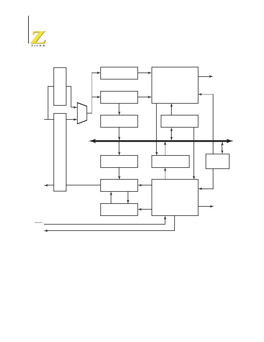
LIN-UART
P R E L I M I N A R Y PS024604-1005
Z8 Encore!
�
Motor Control Flash MCUs
Product Specification
112
Data Format for Standard UART Modes
The LIN-UART always transmits and receives data in an 8-bit data format, least-signifi-
cant bit first. An even or odd parity bit or multiprocessor address/data bit can be optionally
added to the data stream. Each character begins with an active low Start bit and ends with
either 1 or 2 active high Stop bits. Figures 12 and 13 illustrate the asynchronous data for-
mat employed by the LIN-UART without parity and with parity, respectively.
Figure 11. LIN-UART Block Diagram
RxD
IrDA
Noise Filter
TxD
Parity Checker
System Bus
Receive Shifter
Parity Generator
Status Registers
Baud Rate
Generator
Control Registers
Rx IRQ
Tx IRQ
Transmitter Control
Receiver Control
with Address Compare
Receive Data
Register
Transmit Data
Register
Transmit Shift
Register
CTS
DE
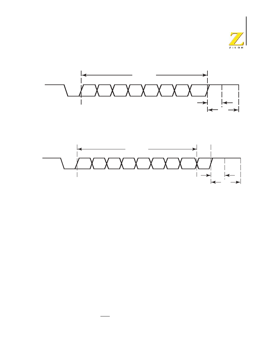
PS024604-1005
P R E L I M I N A R Y
Transmitting Data using the Polled Method
Z8FMC16100 Series Flash MCU
Product Specification
113
Transmitting Data using the Polled Method
Follow these steps to transmit data using the polled operating method:
1. Write to the LIN-UART Baud Rate High and Low Byte registers to set the appropriate
baud rate.
2. Enable the LIN-UART pin functions by configuring the associated GPIO port pins for
alternate function operation.
3. If MULTIPROCESSOR mode is appropriate, write to the LIN-UART Control 1 Reg-
ister to enable MULTIPROCESSOR (9-bit) mode functions.
Set the MULTIPROCESSOR Mode Select (
MPEN
) to Enable MULTIPROCESSOR
mode.
4. Write to the LIN-UART Control 0 Register to:
a. Set the transmit enable bit (
TEN
) to enable the LIN-UART for data transmission
b. If parity is appropriate and multiprocessor mode is not enabled, set the parity
enable bit (
PEN
) and select either even or odd parity (
PSEL
).
c. Set or clear the
CTSE
bit to enable or disable control from the remote receiver
using the CTS pin.
Figure 12. LIN-UART Asynchronous Data Format without Parity
Figure 13. LIN-UART Asynchronous Data Format with Parity
Data Field
Start
Idle State
of Line
Stop Bit(s)
Bit 0
Bit 1
Bit 2
Bit 3
Bit 4
Bit 5
Bit 6
Bit 7
1
1
2
0
lsb
msb
Data Field
Start
Idle State
of Line
Stop Bit(s)
Bit 0
Bit 1
Bit 2
Bit 3
Bit 4
Bit 5
Bit 6
Bit 7
Parity
1
1
2
0
lsb
msb

LIN-UART
P R E L I M I N A R Y PS024604-1005
Z8 Encore!
�
Motor Control Flash MCUs
Product Specification
114
5. Check the
TDRE
bit in the LIN-UART Status 0 register to determine if the Transmit
Data Register is empty (indicated by a 1). If empty, continue to Step 6. If the Transmit
Data Register is full (indicated by a 0), continue to monitor the
TDRE
bit until the
Transmit Data Register becomes available to receive new data.
6. If in MULTIPROCESSOR mode, write the LIN-UART Control 1 Register to select
the outgoing address bit.
Set the Multiprocessor Bit Transmitter (
MPBT
) if sending an address byte; clear it if
sending a data byte.
7. Write the data byte to the LIN-UART Transmit Data Register. The transmitter auto-
matically transfers the data to the Transmit Shift register and transmits the data.
8. If appropriate, and if MULTIPROCESSOR mode is enabled, make any changes to the
Multiprocessor Bit Transmitter (
MPBT
) value.
9. To transmit additional bytes, return to Step 5.
Transmitting Data using the Interrupt-Driven Method
The LIN-UART Transmitter interrupt indicates the availability of the Transmit Data Reg-
ister to accept new data for transmission. Follow these steps to configure the LIN-UART
for interrupt-driven data transmission:
1. Write to the LIN-UART Baud Rate High and Low Byte registers to set the appropriate
baud rate.
2. Enable the LIN-UART pin functions by configuring the associated GPIO port pins for
alternate function operation.
3. Execute a DI instruction to disable interrupts.
4. Write to the Interrupt control registers to enable the LIN-UART Transmitter interrupt
and set the appropriate priority.
5. If multiprocessor mode is appropriate, write to the LIN-UART Control 1 Register to
enable Multiprocessor (9-bit) mode functions.
Set the MULTIPROCESSOR Mode Select (
MPEN
) to Enable MULTIPROCESSOR
mode.
6. Write to the LIN-UART Control 0 Register to:
a. Set the transmit enable bit (
TEN
) to enable the LIN-UART for data transmission
b. If multiprocessor mode is not enabled, enable parity, if appropriate, and select
either even or odd parity.
c. Set or clear the
CTSE
bit to enable or disable control from the remote receiver via
the CTS pin.

PS024604-1005
P R E L I M I N A R Y
Receiving Data using the Polled Method
Z8FMC16100 Series Flash MCU
Product Specification
115
7. Execute an EI instruction to enable interrupts.
The LIN-UART is now configured for interrupt-driven data transmission. Because the
LIN-UART Transmit Data Register is empty, an interrupt is generated immediately. When
the LIN-UART Transmit interrupt is detected, and there is transmit data ready to send, the
associated interrupt service routine (ISR) performs the following:
1. If in MULTIPROCESSOR mode, write the LIN-UART Control 1 Register to select
the outgoing address bit:
Set the Multiprocessor Bit Transmitter (
MPBT
) if sending an address byte, clear it if
sending a data byte.
2. Write the data byte to the LIN-UART Transmit Data Register. The transmitter auto-
matically transfers the data to the Transmit Shift register and transmits the data.
3. Execute the IRET instruction to return from the interrupt-service routine and wait for
the Transmit Data Register to again become empty.
If a transmit interrupt occurs and there is no transmit data ready to send the interrupt-ser-
vice routine will execute the IRET instruction. When the application does have data to
transmit, software can set the appropriate interrupt request bit in the Interrupt Controller to
initiate a new transmit interrupt. Another alternative would be for software to write the
data to the Transmit Data Register instead of invoking the interrupt-service routine.
Receiving Data using the Polled Method
Follow these steps to configure the LIN-UART for polled data reception:
1. Write to the LIN-UART Baud Rate High and Low Byte registers to set the appropriate
baud rate.
2. Enable the LIN-UART pin functions by configuring the associated GPIO port pins for
alternate function operation.
3. Write to the LIN-UART Control 1 Register to enable MULTIPROCESSOR mode
functions, if appropriate.
4. Write to the LIN-UART Control 0 Register to:
a. Set the receive enable bit (
REN
) to enable the LIN-UART for data reception
b. If multiprocessor mode is not enabled, enable parity, if appropriate, and select
either even or odd parity.
5. Check the
RDA
bit in the LIN-UART Status 0 register to determine if the Receive Data
Register contains a valid data byte (indicated by a 1). If
RDA
is set to 1 to indicate
available data, continue to Step 6. If the Receive Data Register is empty (indicated by
a 0), continue to monitor the RDA bit awaiting reception of the valid data.

LIN-UART
P R E L I M I N A R Y PS024604-1005
Z8 Encore!
�
Motor Control Flash MCUs
Product Specification
116
6. Read data from the LIN-UART Receive Data Register. If operating in MULTIPRO-
CESSOR (9-bit) mode, further actions may be required depending on the Multiproces-
sor Mode bits
MPMD
[1:0].
7. Return to Step 5 to receive additional data.
Receiving Data using the Interrupt-Driven Method
The LIN-UART Receiver interrupt indicates the availability of new data (as well as error
conditions). Follow these steps to configure the LIN-UART receiver for interrupt-driven
operation:
1. Write to the LIN-UART Baud Rate High and Low Byte registers to set the appropriate
baud rate.
2. Enable the LIN-UART pin functions by configuring the associated GPIO port pins for
alternate function operation.
3. Execute a DI instruction to disable interrupts.
4. Write to the Interrupt control registers to enable the LIN-UART Receiver interrupt and
set the appropriate priority.
5. Clear the LIN-UART Receiver interrupt in the applicable Interrupt Request Register.
6. Write to the LIN-UART Control 1 Register to enable MULTIPROCESSOR (9-bit)
mode functions, if appropriate.
a. Set the MULTIPROCESSOR Mode Select (
MPEN
) to Enable Multiprocessor
mode.
b. Set the MULTIPROCESSOR Mode Bits,
MPMD[1:0],
to select the appropriate
address matching scheme.
c. Configure the LIN-UART to interrupt on received data and errors or errors only
(interrupt on errors only is unlikely to be useful for Z8FMC16100 Series Flash
MCU devices without a DMA block),
7. Write the device address to the Address Compare Register (automatic multiprocessor
modes only).
8. Write to the LIN-UART Control 0 Register to:
a. Set the receive enable bit (
REN
) to enable the LIN-UART for data reception
b. If MULTIPROCESSOR mode is not enabled, enable parity, if appropriate, and
select either even or odd parity.
9. Execute an EI instruction to enable interrupts.
The LIN-UART is now configured for interrupt-driven data reception. When the LIN-
UART Receiver interrupt is detected, the associated interrupt service routine (ISR) per-
forms the following:

PS024604-1005
P R E L I M I N A R Y
Clear To Send Operation
Z8FMC16100 Series Flash MCU
Product Specification
117
1. Check the LIN-UART Status 0 register to determine the source of the interrupt - error,
break, or received data.
2. If the interrupt was due to data available, read the data from the LIN-UART Receive
Data Register. If operating in MULTIPROCESSOR (9-bit) mode, further actions may
be required depending on the multiprocessor mode bits
MPMD
[1:0].
3. Execute the IRET instruction to return from the interrupt-service routine and await
more data.
Clear To Send Operation
The Clear To Send (CTS) pin, if enabled by the
CTSE
bit of the LIN-UART Control 0 Reg-
ister, performs flow control on the outgoing transmit data stream. The Clear To Send
(CTS) input pin is sampled one system clock before beginning any new character trans-
mission. To delay transmission of the next data character, an external receiver must deas-
sert CTS at least one system clock cycle before a new data transmission begins. For
multiple character transmissions, this operation is typically performed during the Stop Bit
transmission. If CTS deasserts in the middle of a character transmission, the current char-
acter is sent completely.
External Driver Enable
The LIN-UART provides a Driver Enable (DE) signal for off-chip bus transceivers. This
feature reduces the software overhead associated with using a GPIO pin to control the
transceiver when communicating on a multitransceiver bus, such as RS-485.
Driver Enable is a programmable polarity signal that envelopes the entire transmitted data
frame including parity and Stop bits as illustrated in Figure 14. The Driver Enable signal
asserts when a byte is written to the LIN-UART Transmit Data Register. The Driver
Enable signal asserts at least one bit period and no greater than two bit periods before the
Start bit is transmitted. This allows a setup time to enable the transceiver. The Driver
Enable signal deasserts one system clock period after the last
Stop
bit is transmitted. This
one system clock delay allows both time for data to clear the transceiver before disabling
it, as well as the ability to determine if another character follows the current character. In
the event of back to back characters (new data must be written to the Transmit Data Regis-
ter before the previous character is completely transmitted) the DE signal is not deasserted
between characters. The
DEPOL
bit in the LIN-UART Control Register 1 sets the polarity
of the Driver Enable signal.

LIN-UART
P R E L I M I N A R Y PS024604-1005
Z8 Encore!
�
Motor Control Flash MCUs
Product Specification
118
The Driver Enable to
START
bit set-up time is calculated as follows:
LIN-UART Special Modes
The special modes of the LIN-UART are:
�
Multiprocessor Mode
�
LIN Mode
The LIN-UART features a common control register (Control 0) that contains a unique reg-
ister address and several mode-specific control registers (Multiprocessor Control, Noise
Filter Control, and LIN Control) that share a common register address (Control 1). When
the Control 1 address is read or written, the
MSEL[2:0]
(Mode Select) field of the Mode
Select and Status Register determines which physical register is accessed. Similarly, there
are mode-specific status registers, one of which is returned when the Status 0 Register is
read, depending on the
MSEL
field.
Multiprocessor Mode
The LIN-UART features a MULTIPROCESSOR (9-bit) mode that uses an extra (9th) bit
for selective communication when a number of processors share a common UART bus. In
MULTIPROCESSOR mode (also referred to as 9-Bit mode), the multiprocessor bit (
MP
) is
transmitted immediately following the 8-bits of data and immediately preceding the
Stop
bit(s) as illustrated in Figure 15. The character format is:
Figure 14. LIN-UART Driver Enable Signal Timing
(shown with 1 Stop Bit and Parity)
1
� DE to Start Bit Setup Time(s) �
2
Baud Rate (Hz)
Baud Rate (Hz)
Data Field
Start
Idle State
of Line
Stop Bit(s)
Bit 0
Bit 1
Bit 2
Bit 3
Bit 4
Bit 5
Bit 6
Bit 7
Parity
1
1
0
1
0
DE
lsb
msb
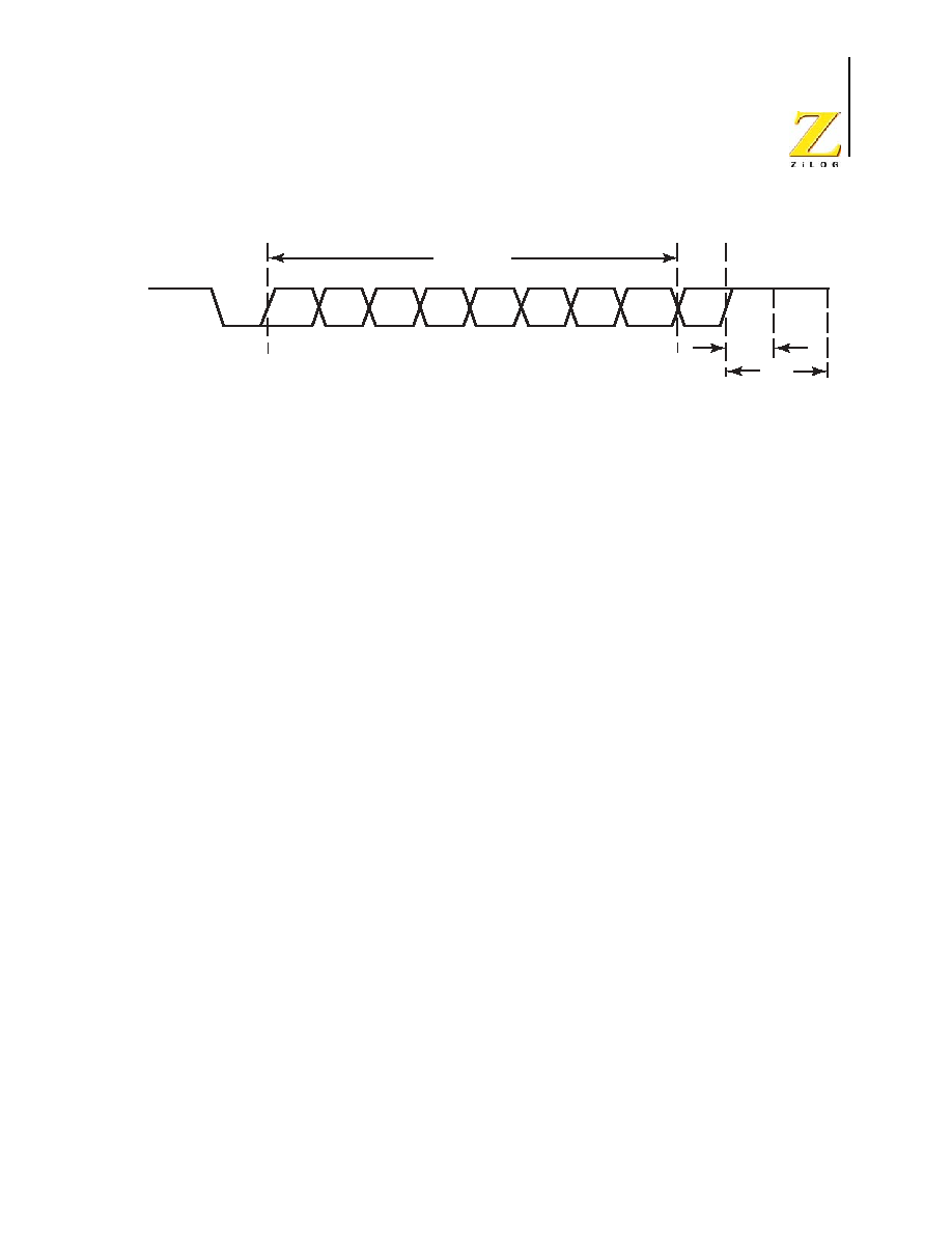
PS024604-1005
P R E L I M I N A R Y Multiprocessor
Mode
Z8FMC16100 Series Flash MCU
Product Specification
119
In Multiprocessor (9-bit) mode, the Parity bit location (9th bit) becomes the MULTIPRO-
CESSOR control bit. The LIN-UART Control 1 and Status 1 registers provide MULTI-
PROCESSOR (9-bit) mode control and status information. If an automatic address
matching scheme is enabled, the LIN-UART Address Compare register holds the network
address of the device.
Multiprocessor Mode Receive Interrupts
When MULTIPROCESSOR (9-bit) mode is enabled, the LIN-UART processes only
frames addressed to it. The determination of whether a frame of data is addressed to the
LIN-UART can be made in hardware, software or a combination of the two, depending on
the multiprocessor configuration bits. In general, the address compare feature reduces the
load on the CPU, because it does not need to access the LIN-UART when it receives data
directed to other devices on the multinode network. The following three MULTIPROCES-
SOR modes are available in hardware:
�
Interrupt on all address bytes
�
Interrupt on matched address bytes and correctly framed data bytes
�
Interrupt only on correctly framed data bytes
These modes are selected with
MPMD[1:0]
in the LIN-UART Control 1 Register. For all
multiprocessor modes, bit
MPEN
of the LIN-UART Control 1 Register must be set to 1.
The first scheme is enabled by writing
01b
to
MPMD[1:0]
. In this mode, all incoming
address bytes cause an interrupt, while data bytes never cause an interrupt. The interrupt
service routine checks the address byte that triggered the interrupt. If it matches the LIN-
UART address, the software clears
MPMD[0]
. At this point, each new incoming byte
interrupts the CPU. The software determines the end of the frame and checks for it by
reading the
MPRX
bit of the LIN-UART Status 1 Register for each incoming byte. If
MPRX
=1, a new frame has begun. If the address of this new frame is different from the
LIN-UART's address, then
MPMD[0]
must be set to 1 by software, causing the LIN-
UART interrupts to go inactive until the next address byte. If the new frame's address
matches the LIN-UART's, then the data in the new frame is processed as well.
Figure 15. LIN-UART Asynchronous Multiprocessor Mode Data Format
Data Field
Start
Idle State
of Line
Stop Bit(s)
Bit 0
Bit 1
Bit 2
Bit 3
Bit 4
Bit 5
Bit 6
Bit 7
MP
1
1
2
0
lsb
msb

LIN-UART
P R E L I M I N A R Y PS024604-1005
Z8 Encore!
�
Motor Control Flash MCUs
Product Specification
120
The second scheme is enabled by setting MPMD[1:0] to 10B and writing the LIN-UART's
address into the LIN-UART Address Compare Register. This mode introduces more hard-
ware control, interrupting only on frames that match the LIN-UART's address. When an
incoming address byte does not match the LIN-UART's address, it is ignored. All succes-
sive data bytes in this frame are also ignored. When a matching address byte occurs, an
interrupt is issued and further interrupts occur on each successive data byte. The first data
byte in the frame has
NEWFRM
=1 in the LIN-UART Status 1 Register. When the next
address byte occurs, the hardware compares it to the LIN-UART's address. If there is a
match, the interrupt occurs and the
NEWFRM
bit is set for the first byte of the new frame. If
there is no match, the LIN-UART ignores all incoming bytes until the next address match.
The third scheme is enabled by setting
MPMD
[1:0] to
11B
and by writing the LIN-UART's
address into the LIN-UART Address Compare Register. This mode is identical to the sec-
ond scheme, except that there are no interrupts on address bytes. The first data byte of
each frame remains accompanied by a
NEWFRM
assertion.
LIN Protocol Mode
The LIN (Local Interconnect Network) protocol as supported by the LIN-UART module is
defined in rev 2.0 of the LIN Specification Package. The LIN protocol specification cov-
ers all aspects of transferring information between LIN Master and Slave devices using
message frames including error detection and recovery, sleep mode and wake up from
sleep mode. The LIN-UART hardware in LIN mode provides character transfers to sup-
port the LIN protocol including BREAK transmission and detection, WAKE-UP transmis-
sion and detection, and slave autobauding. Part of the error detection of the LIN protocol
is for both master and slave devices to monitor their receive data when transmitting. If the
receive and transmit data streams do not match, the LIN-UART asserts the
PLE
bit (phys-
ical layer error bit in Status0 register). The message frame time-out aspect of the protocol
is left to software, requiring the use of an additional general purpose timer. The LIN mode
of the LIN-UART does not provide any hardware support for computing/verifying the
checksum field or verifying the contents of the Identifier field. These fields are treated as
data and are not interpreted by hardware. The checksum calculation/verification can easily
be implemented in software via the ADC (Add with Carry) instruction.
The LIN bus contains a single master and one or more slaves. The LIN master is responsi-
ble for transmitting the message frame header which consists of the Break, Synch and
Identifier fields. Either the master or one of the slaves transmits the associated response
section of the message which consists of data characters followed by a checksum charac-
ter.
In LIN mode, the interrupts defined for normal UART operation still apply with the fol-
lowing changes.
�
Parity Error (
PE
bit in Status0 register) is redefined as the Physical Layer Error (
PLE
)
bit. The
PLE
bit indicates that receive data does not match transmit data when the LIN-
UART is transmitting. This applies to both Master and Slave operating modes.

PS024604-1005
P R E L I M I N A R Y
LIN Protocol Mode
Z8FMC16100 Series Flash MCU
Product Specification
121
�
The Break Detect interrupt (
BRKD
bit in Status0 register) indicates when a Break is de-
tected by the slave (break condition for at least 11 bit times). Software can use this in-
terrupt to start a timer checking for message frame time-out. The duration of the break
can be read in the
RxBreakLength[3:0]
field of the Mode Status Register.
�
The Break Detect interrupt (
BRKD
bit in Status0 register) indicates when a Wake-up
message has been received if the LIN-UART is in LinSleep state.
�
In LIN slave mode, if the BRG counter overflows while measuring the autobaud period
(Start bit to beginning of bit 7 of autobaud character) an Overrun Error is indicated (
OE
bit in the Status0 register). In this case, software sets the LinState field back to
10b
,
where the Slave ignores the current message and waits for the next Break. The Baud
Reload High and Low registers are not updated by hardware if this autobaud error oc-
curs. The
OE
bit is also set if a data overrun error occurs.
LIN System Clock Requirements
The LIN master provides the timing reference for the LIN network and is required to have
a clock source with a tolerance of �0.5%. A slave with autobaud capability is required to
have a baud clock matching the master oscillator within �14%. The slave nodes autobaud
to lock onto the master timing reference with an accuracy of �2%. If a Slave does not con-
tain autobaud capability it must include a baud clock which deviates from the masters by
no more than �1.5%. These accuracy requirements must include affects such as voltage
and temperature drift during operation.
Before sending/receiving messages, the Baud Reload High/Low registers must be initial-
ized. Unlike standard UART modes, the Baud Reload High/Low registers must be loaded
with the baud interval rather than 1/16 of the baud interval.
In order to autobaud with the required accuracy, the LIN slave system clock must be at
least 100 times the baud rate.
LIN Mode Initialization and Operation
The LIN protocol mode is selected by setting either the
LMST
(LIN Master) or
LSLV
(LIN
Slave), and optionally (for LIN slave) the
ABEN
(Autobaud Enable) bits in the LIN Control
Register. To access the LIN Control Register, the
MSEL
(Mode Select) field of the LIN-
UART Mode Select/Status register must be = 010B. The LIN-UART Control0 register
must be initialized with
TEN
= 1,
REN
= 1, all other bits = 0.
In addition to the
LMST
,
LSLV
and
ABEN
bits in the LIN Control Register, a
Lin-
State
[1:0] field exists that defines the current state of the LIN logic. This field is initially
set by software. In the LIN Slave mode, the
LinState
field is updated by hardware as the
Slave moves through the Wait For Break, AutoBaud, and Active states.
The Noise Filter may also need to be enabled and configured when interfacing to a LIN
bus.

LIN-UART
P R E L I M I N A R Y PS024604-1005
Z8 Encore!
�
Motor Control Flash MCUs
Product Specification
122
LIN MASTER Mode Operation
LIN MASTER mode is selected by setting
LMST
= 1,
LSLV
= 0,
ABEN
= 0,
LinState
[1:0]
=
11B.
If the LIN bus protocol indicates the bus is required go into the LIN sleep state, the
LinState
[1:0] bits must be set =
00B
by software.
The Break is the first part of the message frame transmitted by the master, consisting of at
least 13 bit periods of logical zero on the LIN bus. During initialization of the LIN master,
the duration (in bit times) of the Break is written to the
TxBreakLength
field of the LIN
Control Register. The transmission of the Break is performed by setting the
SBRK
bit in the
Control 0 Register. The LIN-UART starts the Break once the
SBRK
bit is set and any char-
acter transmission currently underway has completed. The
SBRK
bit is deasserted by hard-
ware once the break is completed.
The Synch character is transmitted by writing a
55H
to the Transmit Data Register (
TDRE
must = 1 before writing). The Synch character is not transmitted by the hardware until
after the Break is complete.
The Identifier character is transmitted by writing the appropriate value to the Transmit
Data Register (
TDRE
must = 1 before writing).
If the master is sending the response portion of the message, these data and checksum
characters are written to the Transmit Data Register when the
TDRE
bit asserts. If the trans-
mit data register is written after
TDRE
asserts, but before
TXE
asserts, the hardware inserts
one or two stop bits between each character as determined by the
Stop
bit in the Control0
register. Additional idle time occurs between characters if
TXE
asserts before the next
character is written.
If the selected slave is sending the response portion of the frame to the master, each
receive byte will be signalled by the receive data interrupt (
RDA
bit will be set in the
Status0 register).
If the selected slave is sending the response to a different slave, the master can ignore the
response characters by deasserting the
REN
bit in the Control0 register until the frame time
slot has completed.
LIN Sleep Mode
While the LIN bus is in the sleep state, the CPU can be in either low power STOP mode, in
HALT mode, or in normal operational state. Any device on the LIN bus may issue a Wake-
up message if it requires the master to initiate a LIN message frame. Following the Wake-
up message, the master wakes up and initiates a new message. A Wake-up message is
accomplished by pulling the bus low for at least 250 �s but less than 5 ms. Transmitting a
00h
character is one way to transmit the wake-up message.
If the CPU is in STOP mode, the LIN-UART is not active and the Wake-up message must
be detected by a GPIO edge detect Stop-Mode Recovery. The duration of the Stop-Mode
Recovery sequence may preclude making an accurate measurement of the Wake-up mes-
sage duration.

PS024604-1005
P R E L I M I N A R Y
LIN Protocol Mode
Z8FMC16100 Series Flash MCU
Product Specification
123
If the CPU is in HALT or operational mode, the LIN-UART (if enabled) times the duration
of the Wake-up and provides an interrupt following the end of the break sequence if the
duration is
3 bit times. The total duration of the Wake-up message in bit times may be
obtained by reading the
RxBreakLength
field in the Mode Status register. After a Wake-
up message has been detected, the LIN-UART can be placed (by software) into either LIN
Master or LIN Slave Wait for Break states as appropriate. If the break duration exceeds 15
bit times, the
RxBreakLength
field contains the value
Fh
. If the LIN-UART is disabled,
the Wake-up message can be detected via a port pin interrupt and timed by software. If the
device is in STOP mode, the high to low transition on the port pin will bring the device out
of STOP mode.
The LIN Sleep state is selected by software setting
LinState
[1:0] = 00. The decision to
move from an active state to sleep state is based on the LIN messages as interpreted by
software.
LIN Slave Operation
LIN Slave mode is selected by setting
LMST
= 0,
LSLV
= 1,
ABEN
= 1 or 0 and
Lin-
State
[1:0] =
01b
(Wait for Break State). The LIN slave detects the start of a new mes-
sage by the Break which appears to the Slave as a break of at least 11 bit times in duration.
The LIN-UART detects the Break and generates an interrupt to the CPU. The duration of
the Break is observable in the
RxBreakLength
field of the Mode Status register. A Break
of less than 11 bit times in duration does not generate a break interrupt when the LIN-
UART is in Wait for Break state. If the Break duration exceeds 15 bit times, the
RxBreak-
Length
field contains the value
Fh
.
Following the Break the LIN-UART hardware automatically transitions to the Autobaud
state, where it autobauds by timing the duration of the first 8 bit times of the Synch charac-
ter as defined in the standard. At the end of the autobaud period, the duration measured by
the BRG counter (auto baud period divided by 8) is automatically transferred to the Baud
Reload High and Low registers if the
ABEN
bit of the LIN control register is set. If the
BRG Counter overflows before reaching the start of bit 7 in the autobaud sequence the
Autobaud Overrun Error interrupt occurs, the
OE
bit in the Status0 register is set and the
Baud Reload registers are not updated. To autobaud within 2% of the master's baud rate,
the slave system clock must be a minimum of 100 times the baud rate. To avoid an auto-
baud overrun error, the system clock must not be greater than 2
19
times the baud rate (16
bit counter following 3-bit prescaler when counting the 8 bit times of the Autobaud
sequence).
Following the Synch character, the LIN-UART hardware transitions to the Active state
where the Identifier character is received and the characters of the Response section of the
message are sent or received. The Slave remains in the Active state until a Break is
received or software forces a state change. Once in Active State (autobaud has completed),
a Break of 10 or more bit times is recognized and will cause a transition to the Autobaud
state.

LIN-UART
P R E L I M I N A R Y PS024604-1005
Z8 Encore!
�
Motor Control Flash MCUs
Product Specification
124
If the Identifier character indicates that this slave device is not participating in the mes-
sage, software can set the
LinState[1:0]
=
01b
(Wait for Break State) to ignore the rest
of the message. No further receive interrupts will occur until the next Break.
LIN-UART Interrupts
The LIN-UART features separate interrupts for the transmitter and receiver. In addition,
when the LIN-UART primary functionality is disabled, the Baud Rate Generator can also
function as a basic timer with interrupt capability.
Transmitter Interrupts
The transmitter generates a single interrupt when the Transmit Data Register Empty bit
(
TDRE
) is set to 1. This indicates that the transmitter is ready to accept new data for trans-
mission. The TDRE interrupt occurs when the transmitter is initially enabled and after the
Transmit shift register has shifted the first bit of a character out. At this point, the Transmit
Data Register may be written with the next character to send. This provides 7 bit periods
of latency to load the Transmit Data Register before the Transmit shift register completes
shifting the current character. Writing to the LIN-UART Transmit Data Register clears the
TDRE
bit to 0.
Receiver Interrupts
The receiver generates an interrupt when any of the following occurs:
�
A data byte has been received and is available in the LIN-UART Receive Data Regis-
ter. This interrupt can be disabled independent of the other receiver interrupt sources
via the
RDAIRQ
bit (this feature is useful in devices which support DMA). The received
data interrupt occurs once the receive character has been placed in the Receive Data
Register. Software must respond to this received data available condition before the
next character is completely received to avoid an overrun error.
In MULTIPROCESSOR mode (
MPEN
= 1), the receive data interrupts are dependent on
the multiprocessor configuration and the most recent address byte
�
A break is received
�
A receive data overrun or LIN slave autobaud overrun error is detected.
�
A data framing error is detected
�
A parity error is detected (physical layer error in LIN mode)
LIN-UART Overrun Errors
When an overrun error condition occurs the LIN-UART prevents overwriting of the valid
data currently in the Receive Data Register. The Break Detect and Overrun status bits are
not displayed until after the valid data has been read.
Note:

PS024604-1005
P R E L I M I N A R Y LIN-UART
Interrupts
Z8FMC16100 Series Flash MCU
Product Specification
125
After the valid data has been read, the
OE
bit of the Status 0 register is updated to indicate
the overrun condition (and Break Detect, if applicable). The
RDA
bit is set to 1 to indicate
that the Receive Data Register contains a data byte. However, because the overrun error
occurred, this byte may not contain valid data and must be ignored. The
BRKD
bit indicates
if the overrun was caused by a break condition on the line. After reading the status byte
indicating an overrun error, the Receive Data Register must be read again to clear the error
bits in the LIN-UART Status 0 register.
In LIN mode, an Overrun Error is signaled for receive data overruns as described above
and in the LIN Slave if the BRG Counter overflows during the autobaud sequence (the
ATB
bit will also be set in this case). There is no data associated with the autobaud over-
flow interrupt, however the Receive Data Register must be read to clear the
OE
bit. In this
case software must write a 10B to the
LinState
field, forcing the LIN slave back to a
Wait for Break state.
LIN-UART Data- and Error-Handling Procedure
Figure 16 illustrates the recommended procedure for use in LIN-UART receiver interrupt
service routines.

LIN-UART
P R E L I M I N A R Y PS024604-1005
Z8 Encore!
�
Motor Control Flash MCUs
Product Specification
126
Baud Rate Generator Interrupts
If the
BRGCTL
bit of the Multiprocessor Control Register (LIN-UART Control 1 Register
with MSEL =
000b
) register is set, and the
REN
bit of the Control 0 Register is 0, the LIN-
UART Receiver interrupt asserts when the LIN-UART Baud Rate Generator reloads. This
action allows the Baud Rate Generator to function as an additional counter if the LIN-
UART receiver functionality is not employed.
Figure 16. LIN-UART Receiver Interrupt Service Routine Flow
Receiver
Ready
Receiver
Interrupt
Read Status
Errors?
No
Yes
Discard data
Read data
Read data that clears
the RDA bit and
resets the error bits

PS024604-1005
P R E L I M I N A R Y
LIN-UART Baud Rate Generator
Z8FMC16100 Series Flash MCU
Product Specification
127
The transmitter can be enabled in this mode.
LIN-UART Baud Rate Generator
The LIN-UART Baud Rate Generator creates a lower frequency baud rate clock for data
transmission. The input to the Baud Rate Generator is the system clock. The LIN-UART
Baud Rate High and Low Byte registers combine to create a 16-bit baud rate divisor value
(
BRG
[15:0]) that sets the data transmission rate (baud rate) of the LIN-UART. The LIN-
UART data rate is calculated using the following equation for normal UART operation:
The LIN-UART data rate is calculated using the following equation for LIN mode UART
operation:
When the LIN-UART is disabled, the Baud Rate Generator can function as a basic 16-bit
timer with interrupt on time-out. To configure the Baud Rate Generator as a timer with
interrupt on time-out, complete the following procedure:
1. Disable the LIN-UART receiver by clearing the
REN
bit in the LIN-UART Control 0
Register to 0 (
TEN
bit may be asserted, transmit activity may occur).
2. Load the appropriate 16-bit count value into the LIN-UART Baud Rate High and Low
Byte registers.
3. Enable the Baud Rate Generator timer function and associated interrupt by setting the
BRGCTL
bit in the LIN-UART Control 1 Register to 1.
Noise Filter
A noise filter circuit is included which filters noise on a digital input signal (such as UART
Receive Data) before the data is sampled by the block. This is likely to be a requirement
for protocols with a noisy environment.
The noise filter contains the following features:
�
Synchronizes the receive input data to the System Clock
�
Noise Filter Enable (
NFEN
) input selects whether the noise filter is bypassed (
NFEN
=
0) or included (
NFEN = 1
) in the receive data path.
UART Data Rate (bits/s) =
System Clock Frequency (Hz)
16 x UART Baud Rate Divisor Value
UART Data Rate (bits/s) =
System Clock Frequency (Hz)
UART Baud Rate Divisor Value
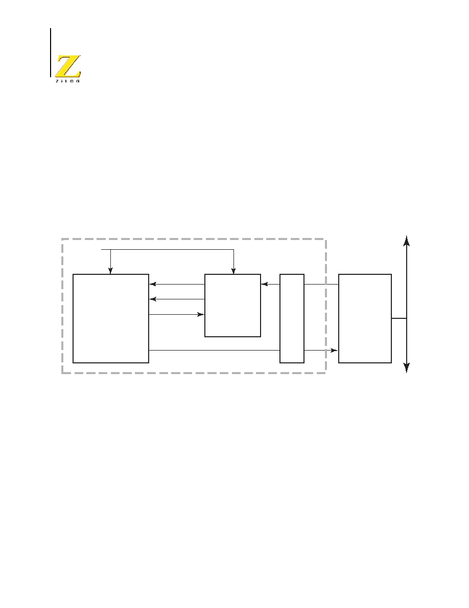
LIN-UART
P R E L I M I N A R Y PS024604-1005
Z8 Encore!
�
Motor Control Flash MCUs
Product Specification
128
�
Noise Filter Control (
NFCTL[2:0]
) input selects the width of the up/down saturating
counter digital filter. The available widths range from 4 bits to 11 bits.
�
The digital filter output features hysteresis
�
Provides an active low Saturated State output (
FiltSatB
) which is used as an indica-
tion of the presence of noise.
Architecture
Figure 17 illustrates how the noise filter is integrated with the LIN-UART for use on a
LIN network.
Operation
The figure below illustrates the operation of the noise filter both with and without noise.
The noise filter in this example is a 2-bit up/down counter which saturates at
00b
and
11b.
A 2-bit counter is shown for convenience, the operation of wider counters is similar.
The output of the filter switches from 1 to 0 when the counter counts down from
01b
to
00b
and switches from 0 to 1 when the counter counts up from
10b
to
11b.
The noise
filter delays the receive data by three System Clock cycles.
The FiltSatB signal is checked when the filtered RxD is sampled in the center of the bit
time. The presence of noise (
FiltSatB = 1
at center of bit time) does not mean the sam-
pled data is incorrect, just that the filter is not in its "saturated" state of all 1's or all 0's. If
FiltSatB = 1 when RxD is sampled during a receive character, the
NE
bit in the
ModeSta-
tus[4:0]
field is set. By observing this bit, an indication of the level of noise in the net-
work can be obtained.
Figure 17. Noise Filter System Block Diagram
RxD
TxD
RxD
TxD
RxD
LIN Bus
TxD
FiltSatB
NFEN, NFCTL
System
Clock
LIN-UART
Noise
Filter
GPIO
LIN
Transceiver
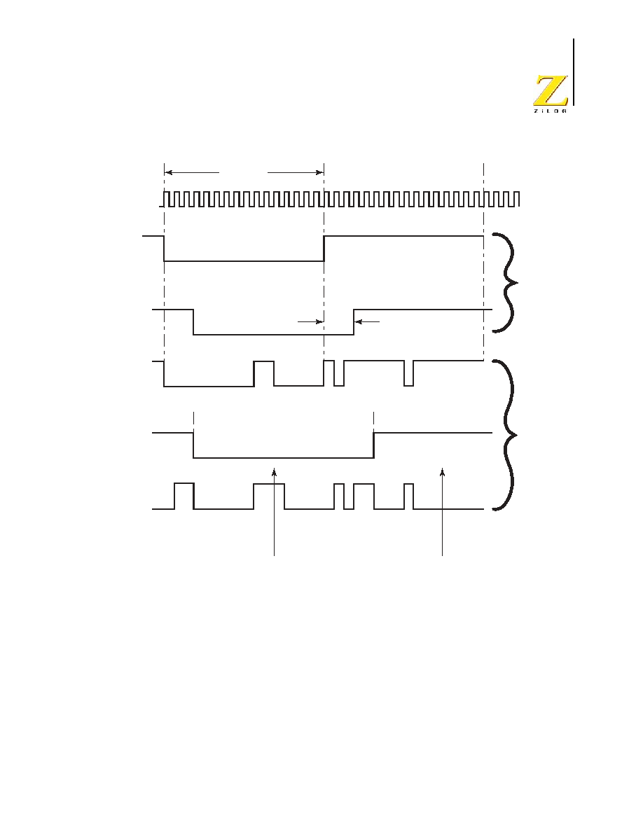
PS024604-1005
P R E L I M I N A R Y Operation
Z8FMC16100 Series Flash MCU
Product Specification
129
Figure 18. Noise Filter Operation
Baud Period
Data Bit = 0
Data Bit = 0
Data Bit = 1
Data Bit = 1
3 3 2 1 0 0 0 0 0 0 0 0 0 0 0 0 0
0 1 2 3 3 3 3 3 3 3 3 3 3 3 3 3 3
3 3 2 1 0 0 0 0 0 0 0 0 0 0 0 0 0
0 1 2 3 3 3 3 3 3 3 3 3 3 3 3 3 3
Nominal filter delay
System
Clock
Input
RxD (ideal)
Noise Filter
Up/Dn Counter
Noise Filter
Output RxD
Input
RxD (noisy)
Noise Filter
Up/Dn Counter
Noise Filter
Output RxD
FiltSatB
Output
UART
Sample Point
Clean RxD
Example
Noise RxD
Example
LIN-UART
P R E L I M I N A R Y PS024604-1005
Z8 Encore!
�
Motor Control Flash MCUs
Product Specification
130
LIN-UART Control Register Definitions
The LIN-UART control registers support the LIN-UART, the associated Infrared Encoder/
Decoder and the noise filter. For more information on the infrared operation, refer to the
Infrared Encoder/Decoder
chapter on page 145.
LIN-UART Transmit Data Register
Data bytes written to the LIN-UART Transmit Data Register, shown in Table 66, are
shifted out on the TxD pin. The Write-only LIN-UART Transmit Data Register shares a
Register File address with the read-only LIN-UART Receive Data Register.
TXD--Transmit Data
LIN-UART transmitter data byte to be shifted out through the TXD pin.
LIN-UART Receive Data Register
Data bytes received through the RxD pin are stored in the LIN-UART Receive Data Reg-
ister, shown in Table 67. The read-only LIN-UART Receive Data Register shares a Regis-
ter File address with the Write-only LIN-UART Transmit Data Register.
Table 66. LIN-UART Transmit Data Register (U0TXD)
BITS
7
6
5
4
3
2
1
0
FIELD
TXD
RESET
X
R/W
W
ADDR
F40H
Table 67. LIN-UART Receive Data Register (U0RXD)
BITS
7
6
5
4
3
2
1
0
FIELD
RXD
RESET
X
R/W
R
ADDR
F40H

PS024604-1005
P R E L I M I N A R Y LIN-UART Status 0 Register
Z8FMC16100 Series Flash MCU
Product Specification
131
RXD--Receive Data
LIN-UART receiver data byte from the RXD pin
LIN-UART Status 0 Register
The LIN-UART Status 0 Register identifies the current LIN-UART operating configura-
tion and status. Table 68 describes the Status 0 Register for standard UART mode.
Table
69
, which follows on page 132, describes the Status0 Register for LIN mode. A more
detailed discussion of each bit follows each table.
Receive Data Available (RDA).
This bit indicates that the LIN-UART Receive Data Reg-
ister has received data. Reading the LIN-UART Receive Data Register clears this bit.
Parity Error (PE).
This bit indicates that a parity error has occurred. Reading the Receive
Data Register clears this bit.
Overrun Error (OE).
This bit indicates that an overrun error has occurred. An overrun
occurs when new data is received and the Receive Data Register has not been read. Read-
ing the Receive Data Register clears this bit.
Framing Error (FE).
This bit indicates that a framing error (no STOP bit following data
reception) was detected. Reading the Receive Data Register clears this bit.
Break Detect (BRKD).
This bit indicates that a break occurred. If the data bits, parity/
multiprocessor bit, and STOP bit(s) are all zeros then this bit is set to 1. Reading the
Receive Data Register clears this bit.
Transmitter Data Register Empty (TDRE).
This bit indicates that the Transmit Data
Register is empty and ready for additional data. Writing to the Transmit Data Register
resets this bit.
Transmitter Empty (TXE).
This bit indicates that the transmit shift register is empty and
character transmission is finished.
Clear To Send Signal (CTS).
When this bit is read it returns the level of the CTS signal.
If LBEN = 1, the CTS input signal is replaced by the internal Receive Data Available sig-
Table 68. LIN-UART Status 0 Register - standard UART mode (U0STAT0)
BITS
7
6
5
4
3
2
1
0
FIELD
RDA
PE
OE
FE
BRKD
TDRE
TXE
CTS
RESET
0
0
0
0
0
1
1
X
R/W
R
R
R
R
R
R
R
R
ADDR
F41H
LIN-UART
P R E L I M I N A R Y PS024604-1005
Z8 Encore!
�
Motor Control Flash MCUs
Product Specification
132
nal to provide flow control in loopback mode. CTS only affects transmission if the CTSE
bit = 1.
Receive Data Available (RDA).
This bit indicates that the Receive Data Register has
received data. Reading the Receive Data Register clears this bit.
Physical Layer Error (PLE).
This bit indicates that transmit and receive data do not
match when a LIN slave or master is transmitting. This could be caused by a fault in the
physical layer or multiple devices driving the bus simultaneously. Reading the Status 0
Register or the Receive Data Register clears this bit.
Receive Data and Autobaud Overrun Error (OE).
This bit is set just as in normal UART
operation if a receive data overrun error occurs. This bit is also set during LIN Slave auto-
baud if the BRG counter overflows before the end of the autobaud sequence, indicating
the receive activity was not an autobaud character or the master baud rate is too slow. The
ATB status bit will also be set in this case. This bit is cleared by reading the Receive Data
Register.
Framing Error (FE).
This bit indicates that a framing error (no STOP bit following data
reception) was detected. Reading the Receive Data Register clears this bit.
Break Detect (BRKD).
This bit is set in LIN mode if (a) in LinSleep state and a break of at
least 4 bit times occurred (Wake-up event) or (b) in Slave Wait Break state and a break of
at least 11 bit times occurred (Break event) or (c) in Slave Active state and a break of at
least 10 bit times occurs. Reading the Status 0 Register or the Receive Data Register clears
this bit.
Transmitter Data Register Empty (TDRE).
This bit indicates that the Transmit Data
Register is empty and ready for additional data. Writing to the Transmit Data Register
resets this bit.
Transmitter Empty (TXE).
This bit indicates that the transmit shift register is empty and
character transmission is finished.
LIN Slave Autobaud Complete (ATB).
This bit is set in LIN SLAVE mode when an auto-
baud character is received. If the ABIEN bit is set in the LIN Control Register, then a
Table 69. LIN-UART Status 0 Register - LIN mode (U0STAT0)
BITS
7
6
5
4
3
2
1
0
FIELD
RDA
PLE
ABOE
FE
BRKD
TDRE
TXE
ATB
RESET
0
0
0
0
0
1
1
0
R/W
R
R
R
R
R
R
R
R
ADDR
F41H
PS024604-1005
P R E L I M I N A R Y LIN-UART
Mode Select and Status Register
Z8FMC16100 Series Flash MCU
Product Specification
133
receive interrupt is generated when this bit is set. Reading the Status 0 Register clears this
bit. This bit will be 0 in LIN MASTER mode.
LIN-UART Mode Select and Status Register
The LIN-UART Mode Select and Status Register, shown in Table 70, contains mode select
and status bits. A more detailed discussion of each bit follows the table.
MSEL--Mode Select.
This R/W field determines which control register is accessed when performing a write or
read to the Uart Control 1 Register address. This field also determines which status is
returned in the ModeStatus field when reading this register.
000 = Multiprocessor and normal UART control/status
001 = Noise Filter control/status
010 = LIN Protocol control/status
011�110: reserved
111 = LIN-UART Hardware Revision (allows hardware revision to be read in the Mode
Status field)
Mode Status. This read-only field returns status corresponding to the mode selected by
MSEL
as follows
000 : Multiprocessor and normal UART mode status = {
NE
, 0, 0,
NEWFRM, MPRX
}
001 : Noise Filter status = {
NE
, 0,0,0,0}
010 : LIN mode status = {
NE, RxBreakLength[3:0
]}
011�110 : reserved = {0, 0, 0, 0, 0}
111 : LIN-UART hardware revision
MULTIPROCESSOR Mode Status field (MSEL = 000B)
NE--Noise Event. This bit is asserted if digital noise is detected on the receive data line
while the data is sampled (center of bit time). If this bit is set, it does not mean that the
receive data is corrupted (though it may be in extreme cases), just that one or more of the
noise filter data samples near the center of the bit time did not match the average data
value.
Table 70. LIN-UART Mode Select and Status Register (U0MDSTAT)
BITS
7
6
5
4
3
2
1
0
FIELD
MSEL
Mode Status
RESET
0
0
0
0
0
0
0
0
R/W
R/W
R/W
R/W
R
R
R
R
R
ADDR
F44H

LIN-UART
P R E L I M I N A R Y PS024604-1005
Z8 Encore!
�
Motor Control Flash MCUs
Product Specification
134
NEWFRM--Status bit denoting the start of a new frame. Reading the LIN-UART Receive
Data register resets this bit to 0.
0 = The current byte is not the first data byte of a new frame.
1 = The current byte is the first data byte of a new frame.
MPRX--Multiprocessor Receive
Returns the value of the last multiprocessor bit received. Reading from the LIN-UART
Receive Data register resets this bit to 0.
Digital Noise Filter Mode Status Field (MSEL =
001B
)
NE--Noise Event. This bit is asserted if digital noise is detected on the receive data line
while the data is sampled (center of bit time). If this bit is set, it does not mean that the
receive data is corrupted (though it may be in extreme cases), just that one or more of the
noise filter data samples near the center of the bit time did not match the average data
value.
LIN Mode Status Field (MSEL =
010B
)
NE--Noise Event. This bit is asserted if some noise level is detected on the receive data
line while the data is sampled (center of bit time). If this bit is set, it does not indicate that
the receive data is corrupt (though it may be in extreme cases), just that one or more of the
16x data samples near the center of the bit time did not match the average data value.
RxBreakLength--LIN mode received break length. This field may be read following a
break (LIN WAKE-UP or BREAK) so software can determine the measured duration of
the break. If the break exceeds 15 bit times the value saturates at
1111B
.
Hardware Revision Mode Status Field (MSEL =
111B
)
This field indicates the hardware revision of the LIN-UART block.
00_xxx LIN UART hardware rev
01_xxx reserved
10_xxx reserved
11_xxx reserved
LIN-UART Control 0 Register
The LIN-UART Control 0 Register, shown in Table 71, configures the basic properties of
the LIN-UART's transmit and receive operations. A more detailed discussion of each bit
follows the table.

PS024604-1005
P R E L I M I N A R Y
LIN-UART Control 0 Register
Z8FMC16100 Series Flash MCU
Product Specification
135
TEN--Transmit Enable
This bit enables or disables the transmitter. The enable is also controlled by the CTS signal
and the CTSE bit. If the CTS signal is Low and the CTSE bit is 1, the transmitter is
enabled.
0 = Transmitter disabled.
1 = Transmitter enabled.
REN--Receive Enable
This bit enables or disables the receiver.
0 = Receiver disabled.
1 = Receiver enabled.
CTSE--CTS Enable
0 = The CTS signal has no effect on the transmitter.
1 = The LIN-UART recognizes the CTS signal as an enable control for the transmitter.
PEN--Parity Enable
This bit enables or disables parity. Even or odd is determined by the PSEL bit.
0 = Parity is disabled. This bit is overridden by the
MPEN
bit.
1 = The transmitter sends data with an additional parity bit and the receiver receives an
additional parity bit.
PSEL--Parity Select
0 = Even parity is transmitted and expected on all received data.
1 = Odd parity is transmitted and expected on all received data.
SBRK--Send Break
This bit pauses or breaks data transmission. Sending a break interrupts any transmission in
progress, so ensure that the transmitter has finished sending data before setting this bit. In
standard UART mode, the duration of the break is determined by how long software
leaves this bit asserted. Also the duration of any required Stop bits following the break
must be timed by software before writing a new byte to be transmitted to the transmit data
register. In LIN mode, the master sends a Break character by asserting
SBRK
. The duration
of the break is timed by hardware, and the
SBRK
bit is deasserted by hardware when the
Break is completed. The duration of the Break is determined by the
TxBreakLength
field
Table 71. LIN-UART Control 0 Register (U0CTL0)
BITS
7
6
5
4
3
2
1
0
FIELD
TEN
REN
CTSE
PEN
PSEL
SBRK
STOP
LBEN
RESET
0
0
0
0
0
0
0
0
R/W
R/W
R/W
R/W
R/W
R/W
R/W
R/W
R/W
ADDR
F42H
LIN-UART
P R E L I M I N A R Y PS024604-1005
Z8 Encore!
�
Motor Control Flash MCUs
Product Specification
136
of the LIN Control register. One or two stop bits are automatically provided by the hard-
ware in LIN mode as defined by the
STOP
bit.
0 = No break is sent.
1 = The output of the transmitter is 0.
STOP--Stop Bit Select
0 = The transmitter sends one stop bit.
1 = The transmitter sends two stop bits.
LBEN--Loop Back Enable
0 = Normal operation.
1 = All transmitted data is looped back to the receiver within the IrDA module.
LIN-UART Control 1 Registers
Multiple registers, shown in Tables 72 through 74) are accessible by a single bus address.
The register selected is determined by the Mode Select (MSEL) field. These registers pro-
vide additional control over LIN-UART operation.
Multiprocessor Control Register
When MSEL =
000b
, the Multiprocessor Control Register, shown in Table 72, provides
control for UART multiprocessor mode, IRDA mode, baud rate timer mode as well as other
features that may apply to multiple modes. A more detailed discussion of each bit follows
the table.
MPMD[1:0]--Multiprocessor Mode
If MULTIPROCESSOR (9-bit) mode is enabled,
00 = The LIN-UART generates an interrupt request on all received bytes (data and
address).
01 = The LIN-UART generates an interrupt request only on received address bytes.
10 = The LIN-UART generates an interrupt request when a received address byte matches
the value stored in the Address Compare Register and on all successive data bytes until an
address mismatch occurs.
Table 72. MultiProcessor Control Register (U0CTL1 with MSEL = 000b)
BITS
7
6
5
4
3
2
1
0
FIELD
MPMD[1]
MPEN
MPMD[0]
MPBT
DEPOL
BRGCTL
RDAIRQ
IREN
RESET
0
0
0
0
0
0
0
0
R/W
R/W
R/W
R/W
R/W
R/W
R/W
R/W
R/W
ADDR
F43H with MSEL = 000b

PS024604-1005
P R E L I M I N A R Y LIN-UART Control 1 Registers
Z8FMC16100 Series Flash MCU
Product Specification
137
11 = The LIN-UART generates an interrupt request on all received data bytes for which
the most recent address byte matched the value in the Address Compare Register.
MPEN--MULTIPROCESSOR (9-bit) Enable
This bit is used to enable MULTIPROCESSOR (9-bit) mode.
0 = Disable Multiprocessor (9-bit) mode.
1 = Enable Multiprocessor (9-bit) mode.
MPBT--Multiprocessor Bit Transmit
This bit is applicable only when Multiprocessor (9-bit) mode is enabled.
0 = Send a 0 in the multiprocessor bit location of the data stream (9th bit).
1 = Send a 1 in the multiprocessor bit location of the data stream (9th bit).
DEPOL--Driver Enable Polarity
0 = DE signal is Active High.
1 = DE signal is Active Low.
BRGCTL--Baud Rate Generator Control
This bit causes different LIN-UART behavior depending on whether the LIN-UART
receiver is enabled (
REN
= 1 in the LIN-UART Control 0 Register).
When the LIN-UART receiver is not enabled, this bit determines whether the Baud Rate
Generator issues interrupts.
0 = BRG is disabled. Reads from the Baud Rate High and Low Byte registers return the
BRG Reload Value
1 = BRG is enabled and counting. The Baud Rate Generator generates a receive interrupt
when it counts down to 0. Reads from the Baud Rate High and Low Byte registers return
the current BRG count value.
When the LIN-UART receiver is enabled, this bit allows reads from the Baud Rate Regis-
ters to return the BRG count value instead of the Reload Value.
0 = Reads from the Baud Rate High and Low Byte registers return the BRG Reload Value.
1 = Reads from the Baud Rate High and Low Byte registers return the current BRG count
value. Unlike the Timers, there is no mechanism to latch the High Byte when the Low
Byte is read.
RDAIRQ--Receive Data Interrupt Enable
0 = Received data and receiver errors generates an interrupt request to the Interrupt Con-
troller.
1 = Received data does not generate an interrupt request to the Interrupt Controller. Only
receiver errors generate an interrupt request.
IREN--Infrared Encoder/Decoder Enable
0 = Infrared Encoder/Decoder is disabled. LIN-UART operates normally.
1 = Infrared Encoder/Decoder is enabled. The LIN-UART transmits and receives data
through the Infrared Encoder/Decoder.

LIN-UART
P R E L I M I N A R Y PS024604-1005
Z8 Encore!
�
Motor Control Flash MCUs
Product Specification
138
Noise Filter Control Register
When MSEL =
001b
, the Noise Filter Control Register, shown in Table , provides control
for the digital noise filter. A more detailed discussion of each bit follows the table.
NFEN--Noise Filter Enable
0 = Noise filter is disabled.
1 = Noise filter is enabled. Receive data is preprocessed by the noise filter.
NFCTL--Noise Filter Control
This field controls the delay and noise rejection characteristics of the noise filter. The
wider the counter the more delay that is introduced by the filter and the wider the noise
event that is filtered.
000 = 4-bit up/down counter
001 = 5-bit up/down counter
010 = 6-bit up/down counter
011 = 7-bit up/down counter
100 = 8-bit up/down counter
101 = 9-bit up/down counter
110 = 10-bit up/down counter
111 = 11-bit up/down counter
LIN Control Register
When
MSEL
=
010b
, the LIN Control Register provides control for the LIN mode of oper-
ation. A more detailed discussion of each bit follows the table.
Table 73. Noise Filter Control Register (U0CTL1 with MSEL = 001b)
BITS
7
6
5
4
3
2
1
0
FIELD
NFEN
NFCTL
Reserved
RESET
0
0
0
0
0
0
0
0
R/W
R/W
R/W
R/W
R/W
R
R
R
R
ADDR
F43H with MSEL = 001b
PS024604-1005
P R E L I M I N A R Y LIN-UART Control 1 Registers
Z8FMC16100 Series Flash MCU
Product Specification
139
LMST--LIN Master Mode
0 = LIN Master Mode not selected
1 = LIN Master Mode selected (if
MPEN, PEN, LSLV
= 0)
LSLV--LIN Slave Mode
0 = LIN Slave Mode not selected
1 = LIN Slave Mode selected (if
MPEN, PEN, LMST
= 0)
ABEN--Autobaud Enable
0 = Autobaud not enabled
1 = Autobaud enabled if in LIN Slave mode.
ABIEN--Autobaud Interrupt Enable
0 = Interrupt following Autobaud does not occur
1 = Interrupt WILL follow Autobaud if in LIN Slave mode and
ABEN
= 1. When the Auto-
baud character is received, a receive interrupt is generated and the
ATB
bit is set in the
Status0 register. There is no receive data associated with this interrupt. The Baud Reload
registers will be updated by hardware with the new bit period value.
LinState[1:0]--LIN State Machine
The LinState is controlled by both hardware and software. Software can force a state
change at any time if necessary. In normal operation, software moves the state in and out
of Sleep state. For a LIN Slave, software changes the state from Sleep to Wait for Break
after which hardware cycles through the Wait for Break, Autobaud and Active states. Soft-
ware changes the state from one of the active states to Sleep state if the LIN bus goes into
Sleep mode. For a LIN Master, software changes the state from Sleep to Active where it
remains until software sets it back to the Sleep state. After configuration software does not
alter the
LinState
field during operation.
00 = Sleep State (either LMST or LSLV may be set)
01 = Wait for Break state (only valid for LSLV = 1)
10 = Autobaud state (only valid for LSLV = 1)
11 = Active state (either LMST or LSLV may be set)
TxBreakLength --Used in LIN mode by the master to control the duration of the transmit-
ted Break.
Table 74. LIN Control Register (U0CTL1 with MSEL = 010b)
BITS
7
6
5
4
3
2
1
0
FIELD
LMST
LSLV
ABEN
ABIEN
LinState[1:0]
TxBreakLength
RESET
0
0
0
0
0
0
0
0
R/W
R/W
R/W
R/W
R/W
R/W
R/W
R/W
R/W
ADDR
F43H with MSEL = 010b

LIN-UART
P R E L I M I N A R Y PS024604-1005
Z8 Encore!
�
Motor Control Flash MCUs
Product Specification
140
00 = 13 bit times
01 = 14 bit times
10 = 15 bit times
11 = 16 bit times
LIN-UART Address Compare Register
The LIN-UART Address Compare Register stores the multinode network address of the
LIN-UART. When the MPMD[1] bit of the LIN-UART Control Register 0 is set, all incom-
ing address bytes are compared to the value stored in this Address Compare Register.
Receive interrupts and RDA assertions only occur in the event of a match. See Table 75.
COMP_ADDR--Compare Address
This 8-bit value is compared to the incoming address bytes.
LIN-UART Baud Rate High and Low Byte Registers
The LIN-UART Baud Rate High and Low Byte registers, shown in Tables 76 and 77)
combine to create a 16-bit baud rate divisor value (BRG[15:0]) that sets the data transmis-
sion rate (baud rate) of the LIN-UART.
Table 75. LIN-UART Address Compare Register (U0ADDR)
BITS
7
6
5
4
3
2
1
0
FIELD
COMP_ADDR
RESET
00H
R/W
R/W
ADDR
F45H
Table 76. LIN-UART Baud Rate High Byte Register (U0BRH)
BITS
7
6
5
4
3
2
1
0
FIELD
BRH
RESET
FFH
R/W
R/W
ADDR
F46H
PS024604-1005
P R E L I M I N A R Y
LIN-UART Baud Rate High and Low Byte
Z8FMC16100 Series Flash MCU
Product Specification
141
The LIN-UART data rate is calculated using the following equation for standard UART
modes. For LIN protocol, the Baud Rate registers must be programmed with the baud
period rather than 1/16 baud period.
The UART must be disabled when updating the Baud Rate registers because the high and
low registers must be written independently.
The LIN-UART data rate is calculated using the following equation for standard UART
operation:
The LIN-UART data rate is calculated using the following equation for LIN mode UART
operation:
For a given LIN-UART data rate, the integer baud rate divisor value is calculated using the
following equation for standard UART operation:
For a given LIN-UART data rate, the integer baud rate divisor value is calculated using the
following equation for LIN mode UART operation:
Table 77. LIN-UART Baud Rate Low Byte Register (U0BRL)
BITS
7
6
5
4
3
2
1
0
FIELD
BRL
RESET
FFH
R/W
R/W
ADDR
F47H
UART Data Rate (bits per second) =
System Clock Frequency (Hz)
16 x UART Baud Rate Divisor Value
UART Data Rate (bits per second) =
System Clock Frequency (Hz)
UART Baud Rate Divisor Value
Note:
UART Baud Rate Divisor Value (BRG)
Round
System Clock Frequency (Hz)
16
x
UART Data Rate (bits/s)
-------------------------------------------------------------------------------
=
UART Baud Rate Divisor Value (BRG)
Round
System Clock Frequency (Hz)
UART Data Rate (bits/s)
-------------------------------------------------------------------------------
=

LIN-UART
P R E L I M I N A R Y PS024604-1005
Z8 Encore!
�
Motor Control Flash MCUs
Product Specification
142
The baud rate error relative to the appropriate baud rate is calculated using the following
equation:
For reliable communication, the LIN-UART baud rate error must never exceed 5 percent.
Tables 78 through 82 provide error data for popular baud rates and commonly-used crystal
oscillator frequencies for normal UART modes of operation.
Table 78. LIN-UART Baud Rates, 20.0 MHz System Clock
Applicable
Rate (kHz)
BRG
Divisor
(Decimal)
Actual Rate
(kHz)
Error(
%)
Applicable
Rate (kHz)
BRG
Divisor
(Decimal)
Actual Rate
(kHz)
Error(
%)
1250.0
1
1250.0
0.00
9.60
130
9.62
0.16
625.0
2
625.0
0.00
4.80
260
4.81
0.16
250.0
5
250.0
0.00
2.40
521
2.399
�0.03
115.2
11
113.64
�1.19
1.20
1042
1.199
�0.03
57.6
22
56.82
�1.36
0.60
2083
0.60
0.02
38.4
33
37.88
�1.36
0.30
4167
0.299
�0.01
19.2
65
19.23
0.16
Table 79. LIN-UART Baud Rates, 10.0 MHz System Clock
Applicable
Rate (kHz)
BRG
Divisor
(Decimal)
Actual Rate
(kHz)
Error(
%)
Applicable
Rate (kHz)
BRG
Divisor
(Decimal)
Actual Rate
(kHz)
Error(
%)
1250.0
N/A
N/A
N/A
9.60
65
9.62
0.16
625.0
1
625.0
0.00
4.80
130
4.81
0.16
250.0
3
208.33
�16.67
2.40
260
2.40
�0.03
115.2
5
125.0
8.51
1.20
521
1.20
�0.03
57.6
11
56.8
�1.36
0.60
1042
0.60
�0.03
38.4
16
39.1
1.73
0.30
2083
0.30
0.2
19.2
33
18.9
0.16
UART Baud Rate Error (%)
100
Actual Data Rate Desired Data Rate
�
Desired Data Rate
----------------------------------------------------------------------------------------------------
�
=

PS024604-1005
P R E L I M I N A R Y
LIN-UART Baud Rate High and Low Byte
Z8FMC16100 Series Flash MCU
Product Specification
143
Table 80. LIN-UART Baud Rates, 5.5296 MHz System Clock
Applicable
Rate (kHz)
BRG
Divisor
(Decimal)
Actual Rate
(kHz)
Error(
%)
Applicable
Rate (kHz)
BRG
Divisor
(Decimal)
Actual Rate
(kHz)
Error(
%)
1250.0
N/A
N/A
N/A
9.60
36
9.60
0.00
625.0
N/A
N/A
N/A
4.80
72
4.80
0.00
250.0
1
345.6
38.24
2.40
144
2.40
0.00
115.2
3
115.2
0.00
1.20
288
1.20
0.00
57.6
6
57.6
0.00
0.60
576
0.60
0.00
38.4
9
38.4
0.00
0.30
1152
0.30
0.00
19.2
18
19.2
0.00
Table 81. LIN-UART Baud Rates, 3.579545 MHz System Clock
Applicable
Rate (kHz)
BRG
Divisor
(Decimal)
Actual Rate
(kHz)
Error(
%)
Applicable
Rate (kHz)
BRG
Divisor
(Decimal)
Actual Rate
(kHz)
Error(
%)
1250.0
N/A
N/A
N/A
9.60
23
9.73
1.32
625.0
N/A
N/A
N/A
4.80
47
4.76
�0.83
250.0
1
223.72
�10.51
2.40
93
2.41
0.23
115.2
2
111.9
�2.90
1.20
186
1.20
0.23
57.6
4
55.9
�2.90
0.60
373
0.60
�0.04
38.4
6
37.3
�2.90
0.30
746
0.30
�0.04
19.2
12
18.6
�2.90
Table 82. LIN-UART Baud Rates, 1.8432 MHz System Clock
Applicable
Rate (kHz)
BRG
Divisor
(Decimal)
Actual Rate
(kHz)
Error(
%)
Applicable
Rate (kHz)
BRG
Divisor
(Decimal)
Actual Rate
(kHz)
Error(
%)
1250.0
N/A
N/A
N/A
9.60
12
9.60
0.00
625.0
N/A
N/A
N/A
4.80
24
4.80
0.00
250.0
N/A
N/A
N/A
2.40
48
2.40
0.00
115.2
1
115.2
0.00
1.20
96
1.20
0.00

LIN-UART
P R E L I M I N A R Y PS024604-1005
Z8 Encore!
�
Motor Control Flash MCUs
Product Specification
144
57.6
2
57.6
0.00
0.60
192
0.60
0.00
38.4
3
38.4
0.00
0.30
384
0.30
0.00
19.2
6
19.2
0.00
Table 82. LIN-UART Baud Rates, 1.8432 MHz System Clock (Continued)
Applicable
Rate (kHz)
BRG
Divisor
(Decimal)
Actual Rate
(kHz)
Error(
%)
Applicable
Rate (kHz)
BRG
Divisor
(Decimal)
Actual Rate
(kHz)
Error(
%)
PS024604-1005
P R E L I M I N A R Y Architecture
Z8FMC16100 Series Flash MCU
Product Specification
145
Infrared Encoder/Decoder
The Z8FMC16100 Series Flash MCU contains two fully-functional, high-performance
UART to Infrared Encoder/Decoders (endecs). Each infrared endec is integrated with an
on-chip UART to allow easy communication between the Z8FMC16100 Series Flash
MCU and IrDA Physical Layer Specification, Version 1.3-compliant infrared transceivers.
Infrared communication provides secure, reliable, low-cost, point-to-point communication
between PCs, PDAs, cell phones, printers and other infrared enabled devices.
Architecture
Figure 19 illustrates the architecture of the infrared endec.
Operation
When the infrared endec is enabled, the transmit data from the associated on-chip UART
is encoded as digital signals in accordance with the IrDA standard and output to the infra-
red transceiver using the
TXD
pin. Likewise, data received from the infrared transceiver is
passed to the infrared endec using the
RXD
pin, decoded by the infrared endec, and passed
Figure 19. Infrared Data Communication System Block Diagram
Baud Rate
Clock
TxD
RxD
Data
I/O
Address
Interrupt
Signal
TxD
RxD
Infrared
Encoder/Decoder
(endec)
UART
System
Clock
TxD
RxD
ZiLOG
ZHX1810
Infrared
Transceiver

Infrared Encoder/Decoder
P R E L I M I N A R Y
PS024604-1005
Z8 Encore!
�
Motor Control Flash MCUs
Product Specification
146
to the UART. Communication is half-duplex, which means simultaneous data transmis-
sion and reception is not allowed.
The baud rate is set by the UART's Baud Rate Generator and supports IrDA standard baud
rates from 9600 baud to 115.2 Kbaud. Higher baud rates are possible, but do not meet
IrDA specifications. The UART must be enabled to use the infrared endec. The infrared
endec data rate is calculated using the following equation:
Transmitting IrDA Data
The data to be transmitted using the infrared transceiver is first sent to the UART. The
UART's transmit signal (TXD) and baud rate clock are used by the IrDA to generate the
modulation signal (IR_TXD) that drives the infrared transceiver. Each UART/Infrared
data bit is 16-clocks wide. If the data to be transmitted is 1, the IR_TXD signal remains
Low for the full 16-clock period. If the data to be transmitted is 0, a 3-clock high pulse is
output following a 7-clock low period. After the 3-clock high pulse, a 6-clock low pulse is
output to complete the full 16-clock data period. Figure 20 illustrates IrDA data transmis-
sion. When the infrared endec is enabled, the UART's TXD signal is internal to the
Z8FMC16100 Series Flash MCU while the IR_TXD signal is output through the
TXD
pin.
Infrared Data Rate (bits/s) =
System Clock Frequency (Hz)
16 x UART Baud Rate Divisor Value
Figure 20. Infrared Data Transmission
16-Clock
Period
3-Clock
Pulse
7-Clock
Delay
Data Bit 0 = 1
Data Bit 1 = 0
Start Bit = 0
Data Bit 2 = 1
Data Bit 3 = 1
Baud Rate
Clock
UART's
TxD
IR_TxD
PS024604-1005
P R E L I M I N A R Y
Receiving IrDA Data
Z8FMC16100 Series Flash MCU
Product Specification
147
Receiving IrDA Data
Data received from the infrared transceiver via the IR_RXD
signal through the
RXD
pin is
decoded by the infrared endec and passed to the UART. The UART's baud rate clock is
used by the infrared endec to generate the demodulated signal (RXD) that drives the
UART. Each UART/Infrared data bit is 16-clocks wide. Figure 21 illustrates data recep-
tion. When the infrared endec is enabled, the UART's RXD signal is internal to the
Z8FMC16100 Series Flash MCU while the IR_RXD signal is received through the
RXD
pin.
The system clock frequency must be at least 1.0 MHz to ensure proper reception of the
1.6 �s minimum-width pulses allowed by the IrDA standard.
Endec Receiver Synchronization
The IrDA receiver uses a local baud rate clock counter (0 to 15 clock periods) to generate
an input stream for the UART and to create a sampling window for detection of incoming
pulses. The generated UART input (UART RXD) is delayed by 8 baud rate clock periods
with respect to the incoming IrDA data stream. When a falling edge in the input data
stream is detected, the endec counter is reset. When the count reaches a value of 8, the
UART RXD value is updated to reflect the value of the decoded data. When the count
reaches 12 baud clock periods, the sampling window for the next incoming pulse opens.
The window remains open until the count again reaches 8 (or in other words 24 baud clock
periods since the previous pulse was detected) giving the endec a sampling window of
minus four baud rate clocks to plus eight baud rate clocks around the expected time of an
Figure 21. Infrared Data Reception
16-Clock
Period
16-Clock
Period
Start Bit = 0
Data Bit 0 = 1
Data Bit 1 = 0
Data Bit 2 = 1
Data Bit 3 = 1
Start Bit = 0
Data Bit 0 = 1
Data Bit 1 = 0
Data Bit 2 = 1
Data Bit 3 = 1
16-Clock
Period
16-Clock
Period
16-Clock
Period
Baud Rate
Clock
Min. 1.6 s
Pulse
8-Clock
Delay
UART's
RxD
IR_RxD
Caution:

Infrared Encoder/Decoder
P R E L I M I N A R Y
PS024604-1005
Z8 Encore!
�
Motor Control Flash MCUs
Product Specification
148
incoming pulse. If an incoming pulse is detected inside this window this process is
repeated. If the incoming data is a logical 1 (no pulse), the endec returns to the initial state
and waits for the next falling edge. As each falling edge is detected, the endec clock
counter is reset, resynchronizing the endec to the incoming signal. This allows the endec
to tolerate jitter and baud rate errors in the incoming data stream. Resynchronizing the
endec does not alter the operation of the UART, which ultimately receives the data. The
UART is only synchronized to the incoming data stream when a Start bit is received.
Infrared Encoder/Decoder Control Register Definitions
All infrared endec configuration and status information is set by the UART control regis-
ters as defined in
LIN-UART Control Register Definitions
section on page 130.
To prevent spurious signals during IrDA data transmission, set the
IREN
bit in the UAR-
Tx Control 1 Register to 1 to enable the Infrared Encoder/Decoder before enabling the
GPIO Port alternate function for the corresponding pin.
Caution:

PS024604-1005
P R E L I M I N A R Y Architecture
Z8FMC16100 Series Flash MCU
Product Specification
149
Serial Peripheral Interface
The Serial Peripheral Interface
(SPI) is a synchronous interface allowing several SPI-type
devices, such as EEPROMs, to be interconnected. SPI features include:
�
Full-duplex, synchronous, character-oriented communication
�
Four-wire interface
�
Data transfer rates up to a maximum of one-half the system clock frequency
�
Error detection
�
Dedicated Baud Rate Generator
Architecture
The SPI can be configured as either a master (in single or multimaster systems) or a slave
as illustrated in Figures 22 through 24.
Figure 22. SPI Configured as a Master in a Single Master, Single Slave System
To Slave s SS Pin
8-Bit Shift Register
Baud Rate
Generator
SPI Master
Bit 0
SCK
MOSI
MISO
SS
Bit 7
From Slave
To Slave
To Slave
Serial Peripheral Interface
P R E L I M I N A R Y
PS024604-1005
Z8 Encore!
�
Motor Control Flash MCUs
Product Specification
150
Figure 23. SPI Configured as a Master in a Single Master, Multiple Slave System
Figure 24. SPI Configured as a Slave
To Slave #1 s SS Pin
8-Bit Shift Register
Baud Rate
Generator
SPI Master
Bit 0
SCK
MOSI
MISO
GPIO
GPIO
V
CC
SS
Bit 7
From Slave
To Slave
To Slave
To Slave #2 s SS Pin
From Master
8-Bit Shift Register
SPI Slave
Bit 7
SCK
MOSI
MISO
SS
Bit 0
To Master
From Master
From Master

PS024604-1005
P R E L I M I N A R Y Operation
Z8FMC16100 Series Flash MCU
Product Specification
151
Operation
The SPI is a full-duplex, synchronous, character-oriented channel that supports a four-wire
interface (serial clock, transmit, receive, and slave select). The SPI block consists of a
transmit/receive shift register, a Baud Rate (clock) Generator, and a control unit.
During an SPI transfer, data is sent and received simultaneously by both the master and the
slave SPI devices. Separate signals are required for data and the serial clock. When an SPI
transfer occurs, a multibit (typically 8-bit) character is shifted out one data pin and an
multibit character is simultaneously shifted in on a second data pin. An 8-bit shift register
in the master and another 8-bit shift register in the slave are connected as a circular buffer.
The SPI shift register is single-buffered in the transmit and receive directions. New data to
be transmitted cannot be written into the shift register until the previous transmission is
complete and receive data (if valid) has been read.
SPI Signals
The four basic SPI signals are:
�
Master-In, Slave-Out (MISO)
�
Master-Out, Slave-In (MOSI)
�
Serial Clock (SCK)
�
Slave Select (SS)
The following paragraphs discuss these SPI signals. Each signal is described in both
MASTER and SLAVE modes.
Master-In, Slave-Out
The Master-In, Slave-Out (MISO) pin is configured as an input in a master device and as
an output in a slave device. It is one of the two lines that transfer serial data, with the most
significant bit sent first. The MISO pin of a slave device is placed in a high-impedance
state if the slave is not selected. When the SPI is not enabled, this signal is in a high-
impedance state.
Master-Out, Slave-In
The Master-Out, Slave-In (MOSI) pin is configured as an output in a master device and as
an input in a slave device. It is one of the two lines that transfer serial data, with the most
significant bit sent first. When the SPI is not enabled, this signal is in a high-impedance
state.

Serial Peripheral Interface
P R E L I M I N A R Y
PS024604-1005
Z8 Encore!
�
Motor Control Flash MCUs
Product Specification
152
Serial Clock
The Serial Clock (SCK) synchronizes data movement both in and out of the device
through its MOSI and MISO pins. In MASTER mode, the SPI's Baud Rate Generator cre-
ates the serial clock. The master drives the serial clock through its own serial clock (SCK)
pin to the slave's SCK pin. When the SPI is configured as a slave, the SCK pin is an input
and the clock signal from the master synchronizes the data transfer between the master and
slave devices. These slave devices ignore the SCK signal unless the SS pin is asserted.
When configured as a slave, the SPI block requires a minimum SCK period of greater than
or equal to 8 times the system (X
IN
) clock period.
The master and slave are each capable of exchanging a character of data during a sequence
of
NUMBITS
clock cycles (refer to the
NUMBITS
field in the SPIMODE Register). In both
master and slave SPI devices, data is shifted on one edge of the SCK and is sampled on the
opposite edge, where data is stable. Edge polarity is determined by the SPI phase and
polarity control.
Slave Select
The active Low Slave Select (SS) input signal selects a slave SPI device. SS must be Low
prior to all data communication to and from the slave device. SS must remain Low for the
full duration of each character transferred. The SS signal may stay Low during the transfer
of multiple characters, or may deassert between each character.
When the SPI is configured as the only master in an SPI system, the SS pin can be set as
either an input or an output. For communication between the Z8 Encore!
�
8K Series
device's SPI master and external slave devices, the SS signal, as an output, can assert the
SS input pin on one of the slave devices. Other GPIO output pins can also be employed to
select external SPI slave devices.
When the SPI is configured as one master in a multimaster SPI system, the SS pin should
be set as an input. The SS input signal on the master must be High. If the SS signal goes
Low (indicating that another master is driving the SPI bus), a collision error flag is set in
the SPI Status Register.
SPI Clock Phase and Polarity Control
The SPI supports four combinations of serial clock phase and polarity using two bits in the
SPI Control Register. The clock polarity bit,
CLKPOL
, selects an active High or active
Low clock and has no effect on the transfer format. Table 83 lists the SPI Clock Phase and
Polarity Operation parameters. The clock phase bit,
PHASE
, selects one of two fundamen-
tally different transfer formats. For proper data transmission, clock phase and polarity
must be identical for the SPI master and the SPI slave. The master always places data on
the MOSI line a half-cycle before the receive clock edge (SCK signal) for the slave to
latch the data.

PS024604-1005
P R E L I M I N A R Y
SPI Clock Phase and Polarity Control
Z8FMC16100 Series Flash MCU
Product Specification
153
Transfer Format Phase Equals Zero
Figure 25 illustrates the timing diagram for an SPI transfer in which
PHASE
is cleared to 0.
The two SCK waveforms show polarity with
CLKPOL
reset to 0 and with
CLKPOL
set to
1. The diagram can be interpreted as either a master or slave timing diagram because the
SCK Master-In/Slave-Out (MISO) and Master-Out/Slave-In (MOSI) pins are directly con-
nected between the master and the slave.
Table 83. SPI Clock Phase and Clock Polarity Operation
PHASE
CLKPOL
SCK Transmit
Edge
SCK Receive
Edge
SCK Idle
State
0
0
Falling
Rising
Low
0
1
Rising
Falling
High
1
0
Rising
Falling
Low
1
1
Falling
Rising
High
Figure 25. SPI Timing When Phase is 0
MOSI
SCK
(CLKPOL = 1)
SCK
(CLKPOL = 0)
Bit 7
Bit 6
Bit 5
Bit 4
Bit 3
Bit 2
Bit 1
Bit 0
MISO
Input Sample Time
SS
Bit 7
Bit 6
Bit 5
Bit 4
Bit 3
Bit 2
Bit 1
Bit 0

Serial Peripheral Interface
P R E L I M I N A R Y
PS024604-1005
Z8 Encore!
�
Motor Control Flash MCUs
Product Specification
154
Transfer Format Phase Equals One
Figure 26 illustrates the timing diagram for an SPI transfer in which
PHASE
is 1. Two
waveforms are depicted for SCK, one for
CLKPOL
reset to 0, and another for
CLKPOL
set
to 1.
Multimaster Operation
In a multimaster SPI system, all SCK pins are tied together, all MOSI pins are tied
together, and all MISO pins are tied together. All SPI pins must then be configured in
OPEN-DRAIN mode to prevent bus contention. At any time, only one SPI device is con-
figured as the master and all other SPI devices on the bus are configured as slaves. The
master enables a single slave by asserting the SS pin on that slave only. Then, the single
master drives data out its SCK and MOSI pins to the SCK and MOSI pins on the slaves
(including those which are not enabled). The enabled slave drives data out its MISO pin to
the MISO master pin.
For a master device operating in a multimaster system, if the SS pin is configured as an
input and is driven Low by another master, the
COL
bit is set to 1 in the SPI Status Regis-
ter. The
COL
bit indicates the occurrence of a multimaster collision (mode fault error con-
dition).
Figure 26. SPI Timing When Phase is 1
MOSI
SCK
(CLKPOL = 1)
SCK
(CLKPOL = 0)
Bit 7
Bit 6
Bit 5
Bit 4
Bit 3
Bit 2
Bit 1
Bit 0
MISO
Input Sample Time
SS
Bit 7
Bit 6
Bit 5
Bit 4
Bit 3
Bit 2
Bit 1
Bit 0

PS024604-1005
P R E L I M I N A R Y Slave
Operation
Z8FMC16100 Series Flash MCU
Product Specification
155
Slave Operation
The SPI block is configured for SLAVE mode operation by setting the SPIEN bit to 1 and
the MMEN bit to 0 in the SPICTL Register and setting the SSIO bit to 0 in the SPIMODE
Register. The
IRQE
,
PHASE
,
CLKPOL
, and
WOR
bits in the SPICTL Register and the
NUM-
BITS
field in the SPIMODE Register must be set to be consistent with the other SPI
devices. The STR bit in the SPICTL Register can be used, if appropriate, to force a start-
up interrupt. The
BIRQ
bit in the SPICTL Register and the
SSV
bit in the SPIMODE Reg-
ister are not used in SLAVE mode. The SPI baud rate generator is not used in SLAVE
mode; therefore, the SPIBRH and SPIBRL registers do not require initialization.
If the slave contains data to send to the master, the data should be written to the SPIDAT
Register before the transaction starts (first edge of SCK when SS is asserted). If the SPI-
DAT Register is not written prior to the slave transaction, the MISO pin outputs the value
that is currently in the SPIDAT Register.
Due to the delay resulting from synchronization of the SPI input signals to the internal sys-
tem clock, the maximum SPICLK baud rate that can be supported in SLAVE mode is the
system clock frequency (X
IN
) divided by 8. This rate is controlled by the SPI master.
Error Detection
The SPI contains error detection logic that supports SPI communication protocols and rec-
ognizes when communication errors have occurred. The SPI Status Register indicates
when a data transmission error has been detected.
Overrun
An overrun error (write collision) indicates that a Write to the SPI Data Register was
attempted while a data transfer is in progress (in either MASTER or SLAVE modes). An
overrun sets the
OVR
bit in the SPI Status Register to 1. Writing a 1 to OVR clears this
error flag. The SPI Data Register is not altered when a Write occurs while a data transfer is
in progress.
Mode Fault
A mode fault indicates when more than one master is trying to communicate at the same
time (a multimaster collision). The mode fault is detected when the enabled master's SS
pin is asserted. A mode fault sets the
COL
bit in the SPI Status Register to 1. Writing a 1 to
COL
clears this error flag.
Slave Mode Abort
In SLAVE mode, if the SS pin deasserts before all bits in a character have been trans-
ferred, the transaction aborts. When this condition occurs, the
ABT
bit is set in the
SPISTAT Register as well as the
IRQ
bit (which indicates that the transaction is complete).

Serial Peripheral Interface
P R E L I M I N A R Y
PS024604-1005
Z8 Encore!
�
Motor Control Flash MCUs
Product Specification
156
The next time SS asserts, the MISO pin outputs SPIDAT[7], regardless of where the previ-
ous transaction suspended. Writing a 1 to
ABT
clears this error flag.
SPI Interrupts
When SPI interrupts are enabled, the SPI generates an interrupt after character transmis-
sion/reception is completed in both MASTER and SLAVE modes. A character can be
defined to be 1�8 bits by the
NUMBITS
field in the SPI Mode Register. In SLAVE mode, it
is not necessary for SS to deassert between characters to generate an interrupt. The SPI in
SLAVE mode can also generate an interrupt if the SS signal deasserts prior to transfer of
all the bits in a character (see description of slave abort error above). Writing a 1 to the
IRQ
bit in the SPI Status Register clears the pending SPI interrupt request. The
IRQ
bit
must be cleared to 0 by the interrupt service routine to generate future interrupts. To start
the transfer process, an SPI interrupt can be forced by software to write a 1 to the STR bit
in the SPICTL Register.
If the SPI is disabled, an SPI interrupt can be generated by a Baud Rate Generator time-
out. This timer function must be enabled by setting the
BIRQ
bit in the SPICTL Register.
This Baud Rate Generator time-out does not set the
IRQ
bit in the SPISTAT Register, just
the SPI interrupt bit in the interrupt controller.
SPI Baud Rate Generator
In SPI MASTER mode, the Baud Rate Generator creates a lower-frequency serial clock
(SCK) for data transmission synchronization between the master and the external slave.
The input to the Baud Rate Generator is from the system clock. The SPI Baud Rate High
and Low Byte registers combine to form a 16-bit reload value, BRG[15:0], for the SPI
Baud Rate Generator. The SPI baud rate is calculated using the following equation:
Minimum baud rate is obtained by setting BRG[15:0] to
0000h
for a clock divisor value
of (2 x 65536 = 131072).
When the SPI is disabled, the Baud Rate Generator can function as a basic 16-bit timer
with an interrupt upon time-out. To configure the Baud Rate Generator as a timer with an
interrupt upon time-out, complete the following procedure:
1. Disable the SPI by clearing the
SPIEN
bit in the SPI Control Register to 0.
2. Load the appropriate 16-bit count value into the SPI Baud Rate High and Low Byte
registers.
3. Enable the Baud Rate Generator timer function and the associated interrupt by setting
the
BIRQ
bit in the SPI Control Register to 1.
SPI Baud Rate (bits/s) =
System Clock Frequency (Hz)
2 x BRG[15:0]

PS024604-1005
P R E L I M I N A R Y
SPI Data Register
Z8FMC16100 Series Flash MCU
Product Specification
157
SPI Data Register
The SPI Data Register stores both the outgoing (transmit) data and the incoming (receive)
data. Reads from the SPI Data Register always return the current contents of the 8-bit shift
register. Data is shifted out starting with bit 7. The last bit received resides in bit position 0.
With the SPI configured as a master, writing a data byte to this register initiates data trans-
mission. With the SPI configured as a slave, writing a data byte to this register loads the
shift register in preparation for the next data transfer with the external master. In either
MASTER or SLAVE mode, if a transmission is already in progress, Writes to this register
are ignored and the overrun error flag,
OVR
, is set in the SPI Status Register.
When character length is less than 8 bits (as set by the
NUMBITS
field in the SPI Mode Reg-
ister), the transmit character must be left-justified in the SPI Data Register. A received char-
acter of less than 8 bits is right-justified (the final bit received is in bit position 0). For
example, if the SPI is configured for 4-bit characters, the transmit characters must be written
to SPIDATA[7:4] and the received characters are read from SPIDATA[3:0]. See Table 84.
DATA--Data
Transmit and/or receive data.
Table 84. SPI Data Register (SPIDATA)
BITS
7
6
5
4
3
2
1
0
FIELD
DATA
RESET
X
R/W
R/W
ADDR
F60H

Serial Peripheral Interface
P R E L I M I N A R Y
PS024604-1005
Z8 Encore!
�
Motor Control Flash MCUs
Product Specification
158
SPI Control Register
The SPI Control Register configures the SPI for transmit and receive operations.
IRQE--Interrupt Request Enable
0 = SPI interrupts are disabled. No interrupt requests are sent to the Interrupt Controller.
1 = SPI interrupts are enabled. Interrupt requests are sent to the Interrupt Controller.
STR--Start an SPI Interrupt Request
0 = No effect.
1 = Setting this bit to 1 also sets the IRQ bit in the SPI Status register to 1. Setting this bit
forces the SPI to send an interrupt request to the Interrupt Control. This bit can be used by
software for a function similar to transmit buffer empty in a UART. Writing a 1 to the
IRQ bit in the SPI Status register clears this bit to 0.
BIRQ--BRG Timer Interrupt Request
If the SPI is enabled, this bit has no effect. If the SPI is disabled:
0 = The Baud Rate Generator timer function is disabled.
1 = The Baud Rate Generator timer function and time-out interrupt are enabled.
PHASE--Phase Select
Sets the phase relationship of the data to the clock. Refer to the SPI Clock Phase and
Polarity Control section for more information on operation of the PHASE bit.
CLKPOL--Clock Polarity
0 = SCK idles Low (0).
1 = SCK idle High (1).
WOR--Wire-OR (Open-Drain) Mode Enabled
0 = SPI signal pins not configured for open-drain.
1 = All four SPI signal pins (SCK, SS, MISO, MOSI) configured for open-drain function.
This setting is typically used for multi-master and/or multi-slave configurations.
MMEN--SPI MASTER Mode Enable
0 = SPI configured in SLAVE mode.
1 = SPI configured in MASTER mode.
Table 85. SPI Control Register (SPICTL)
BITS
7
6
5
4
3
2
1
0
FIELD
IRQE
STR
BIRQ
PHASE
CLKPOL
WOR
MMEN
SPIEN
RESET
00H
R/W
R/W
ADDR
F61H
PS024604-1005
P R E L I M I N A R Y SPI
Status
Register
Z8FMC16100 Series Flash MCU
Product Specification
159
SPIEN--SPI Enable
0 = SPI disabled.
1 = SPI enabled.
SPI Status Register
The SPI Status Register indicates the current state of the SPI. All bits revert to their reset
state if the SPIEN bit in the SPICTL Register = 0.
IRQ--Interrupt Request
If SPIEN = 1, this bit is set if the STR bit in the SPICTL register is set, or upon completion
of an SPI master or slave transaction. This bit does not set if SPIEN = 0 and the SPI Baud
Rate Generator is used as a timer to generate the SPI interrupt.
0 = No SPI interrupt request pending.
1 = SPI interrupt request is pending.
OVR--Overrun
0 = An overrun error has not occurred.
1 = An overrun error has been detected.
COL--Collision
0 = A multi-master collision (mode fault) has not occurred.
1 = A multi-master collision (mode fault) has been detected.
ABT--SLAVE mode transaction abort
This bit is set if the SPI is configured in SLAVE mode, a transaction is occurring and SS
deasserts before all bits of a character have been transferred as defined by the NUMBITS
field of the SPIMODE register. The IRQ bit also sets, indicating the transaction has com-
pleted.
0 = A SLAVE mode transaction abort has not occurred.
1 = A SLAVE mode transaction abort has been detected.
Reserved--Must be 0.
Table 86. SPI Status Register (SPISTAT)
BITS
7
6
5
4
3
2
1
0
FIELD
IRQ
OVR
COL
ABT
Reserved
TXST
SLAS
RESET
0
0
0
0
0
0
0
1
R/W
R/W*
R
ADDR
F62H
R/W* = Read access. Write a 1 to clear the bit to 0.
Serial Peripheral Interface
P R E L I M I N A R Y
PS024604-1005
Z8 Encore!
�
Motor Control Flash MCUs
Product Specification
160
TXST--Transmit Status
0 = No data transmission currently in progress.
1 = Data transmission currently in progress.
SLAS--Slave Select
If SPI enabled as a Slave,
0 = SS input pin is asserted (Low)
1 = SS input is not asserted (High).
If SPI enabled as a Master, this bit is not applicable.
SPI Mode Register
The SPI Mode Register configures the character bit width and the direction and value of
the SS pin.
Reserved--Must be 0.
DIAG - Diagnostic Mode Control bit
This bit is for SPI diagnostics. Setting this bit allows the Baud Rate Generator value to be
read using the SPIBRH and SPIBRL register locations.
0 = Reading SPIBRH, SPIBRL returns the value in the SPIBRH and SPIBRL registers
1 = Reading SPIBRH returns bits [15:8] of the SPI Baud Rate Generator; and reading SPI-
BRL returns bits [7:0] of the SPI Baud Rate Counter. The Baud Rate Counter High and
Low byte values are not buffered.
Exercise caution if reading the values while the BRG is counting.
NUMBITS[2:0]--Number of Data Bits Per Character to Transfer
This field contains the number of bits to shift for each character transfer. Refer to the SPI
Data Register description for information on valid bit positions when the character length
is less than 8-bits.
Table 87. SPI Mode Register (SPIMODE)
BITS
7
6
5
4
3
2
1
0
FIELD
Reserved
DIAG
NUMBITS[2:0]
SSIO
SSV
RESET
00H
R/W
R
R/W
ADDR
F63H
Caution:
PS024604-1005
P R E L I M I N A R Y
SPI Diagnostic State Register
Z8FMC16100 Series Flash MCU
Product Specification
161
000 = 8 bits
001 = 1 bit
010 = 2 bits
011 = 3 bits
100 = 4 bits
101 = 5 bits
110 = 6 bits
111 = 7 bits
SSIO--Slave Select I/O
0 = SS pin configured as an input.
1 = SS pin configured as an output (MASTER mode only).
SSV--Slave Select Value
If SSIO = 1 and SPI configured as a Master:
0 = SS pin driven Low (0).
1 = SS pin driven High (1).
This bit has no effect if SSIO = 0 or SPI configured as a Slave
SPI Diagnostic State Register
The SPI Diagnostic State Register provides observability of internal state. It is a read-only
register used for SPI diagnostics. More detail about each bit follows the table.
SCKEN - Shift Clock Enable
0 = The internal Shift Clock Enable signal is deasserted
1 = The internal Shift Clock Enable signal is asserted (shift register is updates on next sys-
tem clock)
TCKEN - Transmit Clock Enable
0 = The internal Transmit Clock Enable signal is deasserted.
1 = The internal Transmit Clock Enable signal is asserted. When this is asserted the serial
data out is updated on the next system clock (MOSI or MISO).
Table 88. SPI Diagnostic State Register (SPIDST)
BITS
7
6
5
4
3
2
1
0
FIELD
SCKEN
TCKEN
SPISTATE
RESET
00H
R/W
R
ADDR
F64H

Serial Peripheral Interface
P R E L I M I N A R Y
PS024604-1005
Z8 Encore!
�
Motor Control Flash MCUs
Product Specification
162
SPISTATE - SPI State Machine
Defines the current state of the internal SPI State Machine.
SPI Baud Rate High and Low Byte Registers
The SPI Baud Rate High and Low Byte registers combine to form a 16-bit reload value,
BRG[15:0], for the SPI Baud Rate Generator. The SPI baud rate is calculated using the
following equation:
Minimum baud rate is obtained by setting BRG[15:0] to
0000h
for a clock divisor value
of (2 X 65536 = 131072).
BRH = SPI Baud Rate High Byte
Most significant byte, BRG[15:8], of the SPI Baud Rate Generator's reload value.
BRL = SPI Baud Rate Low Byte
Least significant byte, BRG[7:0], of the SPI Baud Rate Generator's reload value.
SPI Baud Rate (bits/s) =
System Clock Frequency (Hz)
2 x BRG[15:0]
Table 89. SPI Baud Rate High Byte Register (SPIBRH)
BITS
7
6
5
4
3
2
1
0
FIELD
BRH
RESET
FFH
R/W
R/W
ADDR
F66H
Table 90. SPI Baud Rate Low Byte Register (SPIBRL)
BITS
7
6
5
4
3
2
1
0
FIELD
BRL
RESET
FFH
R/W
R/W
ADDR
F67H

PS024604-1005
P R E L I M I N A R Y Architecture
Z8FMC16100 Series Flash MCU
Product Specification
163
I
2
C Master/Slave Controller
The I
2
C Master/Slave Controller ensures that the Z8FMC16100 Series Flash MCU
devices are bus-compatible with the I
2
C protocol. The I
2
C bus consists of the serial data
signal (SDA) and a serial clock signal (SCL) bidirectional lines. Features of the I
2
C con-
troller include:
�
Operates in MASTER/SLAVE or SLAVE ONLY modes
�
Supports arbitration in a multimaster environment (MASTER/SLAVE mode)
�
Supports data rates up to 400 Kbps
�
7- or 10-bit slave address recognition (interrupt only on address match)
�
Optional general call address recognition
�
Optional digital filter on receive SDA, SCL lines
�
Optional interactive receive mode allows software interpretation of each received ad-
dress and/or data byte before acknowledging
�
Unrestricted number of data bytes per transfer
�
Baud Rate Generator can be used as a general-purpose timer with an interrupt if the I
2
C
controller is disabled.
Architecture
Figure 27 illustrates the architecture of the I
2
C controller.
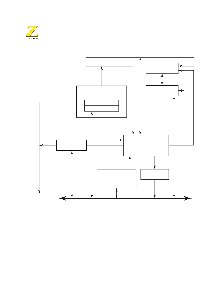
I2C Master/Slave Controller
P R E L I M I N A R Y
PS024604-1005
Z8 Encore!
�
Motor Control Flash MCUs
Product Specification
164
Figure 27. I
2
C Controller Block Diagram
SHIFT
I2CDATA
I2CSTATE
Tx/Rx State Machine
Baud Rate Generator
I2CBRH
I2CBRL
I2CCTL
I2CMODE
I2CSLVAD
I2CISTAT
I
2
C Interrupt
SDA
SCL
Shift
Register Bus
Load

PS024604-1005
P R E L I M I N A R Y I2C
Master/Slave Controller Registers
Z8FMC16100 Series Flash MCU
Product Specification
165
I
2
C Master/Slave Controller Registers
Table 91 summarizes the I
2
C master/slave controller's software-accessible registers.
Comparison with the Master Mode Only I
2
C Controller
Porting code written for the MASTER ONLY I
2
C controller found on other Z8 Encore!
�
parts to the I
2
C Master/Slave Controller is straightforward. The I2CDATA, I2CCTL,
I2CBRH and I2CBRL Register definitions have not changed. The following bullets high-
light the differences between these two designs.
�
The Status (I2CSTATE) Register from the MASTER ONLY I
2
C controller is split into
the Interrupt Status (I2CISTAT) Register and the State (I2CSTATE) Register because
more interrupt sources are available. The
ACK
,
10B
,
TAS
(now called
AS
), and
DSS
(now called
DS
) bits, formerly part of the Status Register, are now part of the State Reg-
ister.
�
The I2CSTATE Register was called the Diagnostic State (I2CDST) Register in the
MASTER-mode-only version. The I2CDST Register provided diagnostic information.
The I2CSTATE Register contains status and state information that may be useful to
software in an operational mode.
�
The I2CMODE Register was called the Diagnostic Control (I2CDIAG) Register in the
MASTER-mode-only version. The I2CMODE Register provides control for the
SLAVE modes of operation, as well as the most significant two bits of the 10-bit slave
address.
Table 91. I
2
C Master/Slave Controller Registers
Name
Abbreviation Description
I
2
C Data
I2CDATA
Transmit/receive data register.
I
2
C Interrupt Status I2CISTAT
Interrupt status register.
I
2
C Control
I2CCTL
Control register--basic control functions.
I
2
C Baud Rate High I2CBRH
High byte of baud rate generator initialization
value.
I
2
C Baud Rate Low I2CBRL
Low byte of baud rate generator initialization
value.
I
2
C State
I2CSTATE
State register.
I
2
C Mode
I2CMODE
Selects MASTER or SLAVE modes, 7- or 10-bit
addressing; configure address recognition, define
slave address bits [9:8].
I
2
C Slave Address
I2CSLVAD
Defines slave address bits [7:0].

I2C Master/Slave Controller
P R E L I M I N A R Y
PS024604-1005
Z8 Encore!
�
Motor Control Flash MCUs
Product Specification
166
�
The I2CSLVAD Register is added to provide programming capabilities for the slave
address.
�
The ACKV bit in the I2CSTATE Register enables the master to check the Acknowl-
edge from the slave before sending the next byte.
�
Support for multimaster environments--if arbitration is lost when operating as a mas-
ter, the ARBLST bit in the I2CISTAT Register is set and the mode automatically
switches to SLAVE mode.
Operation
The I
2
C Master/Slave Controller operates in MASTER/SLAVE mode, SLAVE ONLY
mode, or with master arbitration. In MASTER/SLAVE mode, it can be used as the only
master on the bus or as one of several masters on the bus, with arbitration. In a multimaster
environment, the controller switches from MASTER to SLAVE mode upon losing arbitra-
tion.
Though slave operation is fully supported in MASTER/SLAVE mode, if a device is
intended to operate only as a slave, then SLAVE ONLY mode can be selected. In SLAVE
ONLY mode, the device will not initiate a transaction, even if the software inadvertently
sets the START bit.
SDA and SCL Signals
The I
2
C circuit sends all addresses, data, and Acknowledge signals over the SDA line,
most-significant bit first. SCL is the clock for the I
2
C bus. When the SDA and SCL pin
alternate functions are selected for their respective GPIO ports, the pins are automatically
configured for open-drain operation.
The master is responsible for driving the SCL clock signal. During the Low period of the
clock, a slave can hold the SCL signal Low to suspend the transaction if it is not ready to
proceed. The master releases the clock at the end of the Low period and notices that the
clock remains Low instead of returning to a High level. When the slave releases the clock,
the I
2
C master continues the transaction. All data is transferred in bytes; there is no limit to
the amount of data transferred in one operation. When transmitting address, data, or an
Acknowledge, the SDA signal changes in the middle of the Low period of SCL
.
When
receiving address, Data or an Acknowledge, the SDA signal is sampled in the middle of
the High period of SCL.
A low-pass digital filter can be applied to the SDA and SCL receive signals by setting the
Filter Enable (
FILTEN
) bit in the I
2
C Control Register. When the filter is enabled, any
glitch that is less than a system clock period in width will be rejected. This filter should be
enabled when running in I
2
C FAST mode (400 kbps), and can also be used at lower data
rates.

PS024604-1005
P R E L I M I N A R Y I
2
C Interrupts
Z8FMC16100 Series Flash MCU
Product Specification
167
I
2
C Interrupts
The I
2
C controller contains multiple interrupt sources that are combined into one interrupt
request signal to the interrupt controller. If the I
2
C controller is enabled, the source of the
interrupt is determined by which bits are set in the I2CISTAT Register. If the I
2
C control-
ler is disabled, the BRG controller can be used to generate general-purpose timer inter-
rupts.
Each interrupt source, other than the baud rate generator interrupt, features an associated
bit in the I2CISTAT Register that clears automatically when software reads the register or
performs another task, such as reading/writing the data register.
Transmit Interrupts
Transmit interrupts (
TDRE
bit = 1 in I2CISTAT) occur under the following conditions, both
of which must be true.
�
The transmit data register is empty and the
TXI
bit = 1 in the I
2
C Control Register
�
The I
2
C controller is enabled, with one of the following:
�
The first bit of a 10-bit address is shifted out
�
The first bit of the final byte of an address is shifted out and the
RD
bit is deas-
serted
�
The first bit of a data byte is shifted out
Writing to the I
2
C Data Register always clears the
TRDE
bit to 0.
Receive Interrupts
Receive interrupts (
RDRF
bit = 1 in I2CISTAT) occur when a byte of data has been
received by the I
2
C controller. The
RDRF
bit is cleared by reading from the I
2
C Data Reg-
ister. If the RDRF interrupt is not serviced prior to the completion of the next Receive
byte, the I
2
C controller holds SCL Low during the final data bit of the next byte until
RDRF
is cleared, to prevent receive overruns. A receive interrupt does not occur when a
slave receives an address byte or for data bytes following a slave address that did not
match. An exception is if the Interactive Receive Mode (
IRM
) bit is set in the I2CMODE
Register, in which case Receive interrupts occur for all Receive address and data bytes in
SLAVE mode.
Slave Address Match Interrupts
Slave address match interrupts (
SAM
bit = 1 in I2CISTAT) occur when the I
2
C controller is
in SLAVE mode and an address is received that matches the unique slave address. The
General Call Address (
0000_0000
) and STARTBYTE (
0000_0001
) are recognized if the
GCE
bit = 1 in the I2CMODE Register. The software checks the
RD
bit in the I2CISTAT
Register to determine if the transaction is a Read or Write transaction. The General Call
Address and STARTBYTE address are also distinguished by the
RD
bit. The General Call

I2C Master/Slave Controller
P R E L I M I N A R Y
PS024604-1005
Z8 Encore!
�
Motor Control Flash MCUs
Product Specification
168
Address (
GCA
) bit of the I2CISTAT Register indicates whether the address match occurred
on the unique slave address or the General Call/STARTBYTE address. The
SAM
bit clears
automatically when the I2CISTAT Register is read.
If configured via the
MODE[1:0]
field of the I
2
C Mode Register for 7-bit slave address-
ing, the most significant 7 bits of the first byte of the transaction are compared against the
SLA[6:0]
bits of the Slave Address Register. If configured for 10-bit slave addressing,
the first byte of the transaction is compared against {
11110
,
SLA[9:8]
,R/W} and the sec-
ond byte is compared against
SLA[7:0]
.
Arbitration Lost Interrupts
Arbitration Lost interrupts (
ARBLST
bit = 1 in I2CISTAT) occur when the I
2
C controller is
in MASTER mode and loses arbitration (outputs a 1 on SDA and receives a 0 on SDA).
The I
2
C controller switches to SLAVE mode when this instance occurs. This bit clears
automatically when the I2CISTAT Register is read.
Stop/Restart Interrupts
A Stop/Restart event interrupt (
SPRS
bit = 1 in I2CISTAT) occurs when the I
2
C controller
is in SLAVE mode and a
STOP
or
RESTART
condition is received, indicating the end of the
transaction. The
RSTR
bit in the I2C State Register indicates whether the bit was set due to
a
STOP
or
RESTART
condition. When a restart occurs, a new transaction by the same mas-
ter is expected to follow. This bit is cleared automatically when the I2CISTAT Register is
read. The STOP/RESTART interrupt only occurs on a selected (address match) slave.
Not Acknowledge Interrupts
Not Acknowledge interrupts (
NCKI
bit = 1 in I2CISTAT) occur in MASTER mode when a
Not Acknowledge is received or sent by the I
2
C controller and the
START
or
STOP
bit is
not set in the I
2
C Control Register. In MASTER mode, the Not Acknowledge interrupt
clears by setting the
START
or
STOP
bit. When this interrupt occurs in MASTER mode,
the I
2
C controller waits until it is cleared before performing any action. In SLAVE mode,
the Not Acknowledge interrupt occurs when a Not Acknowledge is received in response to
data sent. The
NCKI
bit clears in SLAVE mode when software reads the I2CISTAT Regis-
ter.
General Purpose Timer Interrupt from Baud Rate Generator
If the I
2
C controller is disabled (
IEN
bit in the I2CCTL Register = 0) and the
BIRQ
bit in
the I2CCTL Register = 1, an interrupt is generated when the baud rate generator (BRG)
counts down to 1. The baud rate generator reloads and continues counting, providing a
periodic interrupt. None of the bits in the I2CISTAT Register are set, allowing the BRG in
the I
2
C controller to be used as a general-purpose timer when the I
2
C controller is dis-
abled.

PS024604-1005
P R E L I M I N A R Y
Start and Stop Conditions
Z8FMC16100 Series Flash MCU
Product Specification
169
Start and Stop Conditions
The master generates the START and STOP conditions to start or end a transaction. To
start a transaction, the I
2
C controller generates a
START
condition by pulling the SDA sig-
nal Low while SCL is High. To complete a transaction, the I
2
C controller generates a
STOP
condition by creating a Low-to-High transition of the SDA signal while the SCL
signal is High. These START
and STOP events occur when the
START
and
STOP
bits in
the I
2
C Control Register are written by software to begin or end a transaction. Any byte
transfer currently under way, including the Acknowledge phase, finishes before the
START or
STOP
condition occurs.
Software Control of I
2
C Transactions
The I
2
C controller is configured via the I
2
C Control and I
2
C Mode registers. The
MODE[1:0]
field of the I
2
C Mode Register allows the configuration of the I
2
C controller
for MASTER/SLAVE or SLAVE ONLY mode, and configures the slave for 7- or 10-bit
addressing recognition.
MASTER/SLAVE mode can be used for:
�
MASTER ONLY operation in a single master/one or more slave I
2
C system
�
MASTER/SLAVE in a multimaster/multislave I
2
C system
�
SLAVE ONLY operation in an I
2
C system
In SLAVE ONLY mode, the START bit of the I
2
C Control Register is ignored (software
cannot initiate a master transaction by accident), and operation to SLAVE ONLY mode is
restricted, thereby preventing accidental operation in MASTER mode.
The software can control I
2
C transactions by enabling the I
2
C controller interrupt in the
interrupt controller or by polling the I
2
C Status Register.
To use interrupts, the I
2
C interrupt must be enabled in the interrupt controller and followed
by executing an EI instruction. The
TXI
bit in the I
2
C Control Register must be set to
enable transmit interrupts. An I
2
C interrupt service routine then checks the I
2
C Status
Register to determine the cause of the interrupt.
To control transactions by polling, the
TDRE
,
RDRF
,
SAM
,
ARBLST
,
SPRS
, and
NCKI
inter-
rupt bits in the I
2
C Status Register should be polled. The
TDRE
bit asserts regardless of the
state of the
TXI
bit.
Master Transactions
The following sections describe master Read and Write transactions to both 7- and 10-bit
slaves.

I2C Master/Slave Controller
P R E L I M I N A R Y
PS024604-1005
Z8 Encore!
�
Motor Control Flash MCUs
Product Specification
170
Master Arbitration
If a master loses arbitration during the address byte, it releases the SDA line, switches to
SLAVE mode and monitors the address to determine if it is selected as a slave. If a master
loses arbitration during the transmission of a data byte, it releases the SDA line and waits
for the next
STOP
or
START
condition.
The master detects a loss of arbitration when a 1 is transmitted but a 0 is received from the
bus in the same bit-time. This loss occurs if more than one master is simultaneously
accessing the bus. Loss of arbitration can occur during the address phase (two or more
masters accessing different slaves) or during the data phase, when the masters are attempt-
ing to write different data to the same slave.
When a master loses arbitration, the software is informed by means of the Arbitration Lost
interrupt. The software can repeat the same transaction at a later time.
A special case can occur when a slave transaction starts just before the software attempts
to start a new master transaction by setting the
START
bit. In this case, the state machine
enters its slave states before the
START
bit is set, and as a result, the I
2
C controller will not
arbitrate. If a slave address match occurs and the I
2
C controller receives/transmits data, the
START
bit is cleared and an Arbitration Lost interrupt is asserted. The software can mini-
mize the chance of this instance occurring by checking the
BUSY
bit in the I2CSTATE
Register before initiating a master transaction. If a slave address match does not occur, the
Arbitration Lost interrupt will not occur, and the
START
bit will not be cleared. The I
2
C
controller will initiate the master transaction after the I
2
C bus is no longer busy.
Master Address-Only Transactions
It is sometimes preferable to perform an address-only transaction to determine if a particu-
lar slave device is able to respond. This transaction can be performed by monitoring the
ACKV
bit in the I2CSTATE Register after the address has been written to the I2CDATA
Register and the
START
bit has been set. After the
ACKV
bit is set, the
ACK
bit in the
I2CSTATE Register determines if the slave is able to communicate. The
STOP
bit must be
set in the I2CCTL Register to terminate the transaction without transferring data. For a 10-
bit slave address, if the first address byte is acknowledged, the second address byte should
also be sent to determine if the preferred slave is responding.
Another approach is to set both the
STOP
and
START
bits (for sending a 7-bit address).
After both bits have cleared (7-bit address has been sent and transaction is complete), the
ACK
bit can be read to determine if the slave has acknowledged. For a 10-bit slave, set the
STOP
bit after the second TDRE interrupt (which indicates that the second address byte is
being sent).
Master Transaction Diagrams
In the following transaction diagrams, the shaded regions indicate the data that is trans-
ferred from the master to the slave, and the unshaded regions indicate the data that is trans-
ferred from the slave to the master. The transaction field labels are defined as follows:

PS024604-1005
P R E L I M I N A R Y Master
Transactions
Z8FMC16100 Series Flash MCU
Product Specification
171
Master Write Transaction with a 7-Bit Address
Figure 28 illustrates the data transfer format from a master to a 7-bit addressed slave
The procedure for a master transmit operation to a 7-bit addressed slave is as follows:
1. The software initializes the
MODE
field in the I
2
C Mode Register for MASTER/
SLAVE mode with either a 7- or 10-bit slave address. The
MODE
field selects the
address width for this mode when addressed as a slave (but not for the remote slave).
The software asserts the
IEN
bit in the I
2
C Control Register.
2. The software asserts the
TXI
bit of the I
2
C Control Register to enable transmit inter-
rupts.
3. The I
2
C interrupt asserts, because the I
2
C Data Register is empty.
4. The software responds to the
TDRE
bit by writing a 7-bit slave address plus the Write
bit (which is cleared to 0) to the I
2
C Data Register.
5. The software sets the
START
bit of the I
2
C Control Register.
6. The I
2
C controller sends a
START
condition to the I
2
C slave.
7. The I
2
C controller loads the I
2
C Shift Register with the contents of the I
2
C Data Reg-
ister.
8. After one bit of the address has been shifted out by the SDA signal, the transmit inter-
rupt asserts.
9. The software responds by writing the transmit data into the I
2
C Data Register.
10. The I
2
C controller shifts the remainder of the address and the Write bit out via the
SDA signal.
11. The I
2
C slave sends an Acknowledge (by pulling the SDA signal Low) during the next
high period of SCL. The I
2
C controller sets the
ACK
bit in the I
2
C Status Register.
S
Start
W
Write
A
Acknowledge
A
Not Acknowledge
P
Stop
S
Slave
Address
W = 0
A
Data
A
Data
A
Data
A/A
P/S
Figure 28. Data Transfer Format--Master Write Transaction with a 7-Bit Address

I2C Master/Slave Controller
P R E L I M I N A R Y
PS024604-1005
Z8 Encore!
�
Motor Control Flash MCUs
Product Specification
172
If the slave does not acknowledge the address byte, the I
2
C controller sets the
NCKI
bit in the I
2
C Status Register, sets the
ACKV
bit, and clears the
ACK
bit in the I
2
C State
Register. The software responds to the Not Acknowledge interrupt by setting the
STOP
bit and clearing the
TXI
bit. The I
2
C controller flushes the Transmit Data Register,
sends a
STOP
condition on the bus, and clears the
STOP
and
NCKI
bits. The transaction
is complete, and the following steps can be ignored.
12. The I
2
C controller loads the contents of the I
2
C Shift Register with the contents of the
I
2
C Data Register.
13. The I
2
C controller shifts the data out via the SDA signal. After the first bit is sent, the
transmit interrupt asserts.
14. If more bytes remain to be sent, return to Step 9.
15. When there is no more data to be sent, the software responds by setting the
STOP
bit of
the I
2
C Control Register (or the
START
bit to initiate a new transaction).
16. If no additional transaction is queued by the master, the software can clear the
TXI
bit
of the I
2
C Control Register.
17. The I
2
C controller completes transmission of the data on the SDA signal.
18. The I
2
C controller sends a
STOP
condition to the I
2
C bus.
If the slave terminates the transaction early by responding with a Not Acknowledge during
the transfer, the I
2
C controller asserts the
NCKI
interrupt and halts. The software must ter-
minate the transaction by setting either the
STOP
bit (end transaction) or the
START
bit
(end this transaction, start a new one). In this case, it is not necessary for software to set
the
FLUSH
bit of the I2CCTL Register to flush the data that was previously written but not
transmitted. The I
2
C controller hardware automatically flushes transmit data in this not
acknowledge case.
Master Write Transaction with a 10-Bit Address
Figure 29 illustrates the data transfer format from a master to a 10-bit addressed slave.
The first seven bits transmitted in the first byte are
11110XX
. The two
XX
bits are the two
most significant bits of the 10-bit address. The lowest bit of the first byte transferred is the
Read/Write control bit (which is cleared to 0). The transmit operation is performed in the
same manner as 7-bit addressing.
The procedure for a master transmit operation to a 10-bit addressed slave is as follows:
S
Slave Address
1st Byte
W=0
A
Slave Address
2nd Byte
A
Data
A
Data
A/A
F/S
Figure 29. Data Transfer Format--Master Write Transaction with a 10-Bit Address
Note:

PS024604-1005
P R E L I M I N A R Y Master
Transactions
Z8FMC16100 Series Flash MCU
Product Specification
173
1. The software initializes the
MODE
field in the I
2
C Mode Register for MASTER/
SLAVE mode with 7- or 10-bit addressing (the I
2
C bus protocol allows the mixing of
slave address types). The
MODE
field selects the address width for this mode when
addressed as a slave (but not for the remote slave). The software asserts the
IEN
bit in
the I
2
C Control Register.
2. The software asserts the
TXI
bit of the I
2
C Control Register to enable transmit inter-
rupts.
3. The I
2
C interrupt asserts because the I
2
C Data Register is empty.
4. The software responds to the
TDRE
interrupt by writing the first slave address byte
(
11110xx0
). The least-significant bit must be 0 for the write operation.
5. The software asserts the
START
bit of the I
2
C Control Register.
6. The I
2
C controller sends a
START
condition to the I
2
C slave.
7. The I
2
C controller loads the I
2
C Shift Register with the contents of the I
2
C Data Reg-
ister.
8. After one bit of the address is shifted out by the SDA signal, the transmit interrupt
asserts.
9. The software responds by writing the second byte of address into the contents of the
I
2
C Data Register.
10. The I
2
C controller shifts the remainder of the first byte of the address and the Write bit
out via the SDA signal.
11. The I
2
C slave sends an Acknowledge by pulling the SDA signal Low during the next
high period of SCL. The I
2
C controller sets the
ACK
bit in the I
2
C Status Register.
If the slave does not acknowledge the first address byte, the I
2
C controller sets the
NCKI
bit in the I
2
C Status Register, sets the
ACKV
bit, and clears the
ACK
bit in the I
2
C
State Register. The software responds to the Not Acknowledge interrupt by setting the
STOP
bit and clearing the
TXI
bit. The I
2
C controller flushes the second address byte
from the data register, sends a
STOP
condition on the bus, and clears the
STOP
and
NCKI
bits. The transaction is complete, and the following steps can be ignored.
12. The I
2
C controller loads the I
2
C Shift Register with the contents of the I
2
C Data Reg-
ister (2nd address byte).
13. The I
2
C controller shifts the second address byte out via the SDA signal. After the
first bit has been sent, the transmit interrupt asserts.
14. The software responds by writing the data to be written out to the I
2
C Control Regis-
ter.
15. The I
2
C controller shifts out the remainder of the second byte of the slave address (or
ensuing data bytes, if looping) via the SDA signal.

I2C Master/Slave Controller
P R E L I M I N A R Y
PS024604-1005
Z8 Encore!
�
Motor Control Flash MCUs
Product Specification
174
16. The I
2
C slave sends an Acknowledge by pulling the SDA signal Low during the next
high period of SCL. The I
2
C controller sets the
ACK
bit in the I
2
C Status Register.
If the slave does not acknowledge, refer to the second paragraph of Step 11.
17. The I
2
C controller shifts the data out by the SDA signal. After the first bit is sent, the
transmit interrupt asserts.
18. If more bytes remain to be sent, return to Step 14.
19. The software responds by asserting the
STOP
bit of the I
2
C Control Register.
20. The I
2
C controller completes transmission of the data on the SDA signal.
21. The I
2
C controller sends a
STOP
condition to the I
2
C bus.
If the slave responds with a Not Acknowledge during the transfer, the I
2
C controller
asserts the
NCKI
bit, sets the
ACKV
bit, clears the
ACK
bit in the I
2
C State Register, and
halts. The software terminates the transaction by setting either the
STOP
bit (end transac-
tion) or the
START
bit (end this transaction, start a new one). The Transmit Data Register
is flushed automatically.
Master Read Transaction with a 7-Bit Address
Figure 30 illustrates the data transfer format for a read operation to a 7-bit addressed slave.
The procedure for a master Read operation to a 7-bit addressed slave is as follows:
1. The software initializes the
MODE
field in the I
2
C Mode Register for MASTER/
SLAVE mode with 7- or 10-bit addressing (the I
2
C bus protocol allows the mixing of
slave address types). The
MODE
field selects the address width for this mode when
addressed as a slave (but not for the remote slave). The software asserts the
IEN
bit in
the I
2
C Control Register.
2. The software writes the I
2
C Data Register with a 7-bit slave address, plus the Read bit
(which is set to 1).
3. The software asserts the
START
bit of the I
2
C Control Register.
4. If this operation is a single-byte transfer, the software asserts the
NAK
bit of the I
2
C
Control Register so that after the first byte of data has been read by the I
2
C controller,
a Not Acknowledge instruction is sent to the I
2
C slave.
5. The I
2
C controller sends a
START
condition.
6. The I
2
C controller sends the address and Read bit out via the SDA signal.
S
Slave Address
R = 1
A
Data
A
Data
A
P/S
Figure 30. Data Transfer Format--Master Read Transaction with a 7-Bit Address
Note:

PS024604-1005
P R E L I M I N A R Y Master
Transactions
Z8FMC16100 Series Flash MCU
Product Specification
175
7. The I
2
C slave acknowledges the address by pulling the SDA signal Low during the
next high period of SCL.
If the slave does not acknowledge the address byte, the I
2
C controller sets the
NCKI
bit in the I
2
C Status Register, sets the
ACKV
bit, and clears the
ACK
bit in the I
2
C State
Register. The software responds to the Not Acknowledge interrupt by setting the
STOP
bit and clearing the
TXI
bit. The I
2
C controller flushes the Transmit Data Register,
sends a
STOP
condition on the bus, and clears the
STOP
and
NCKI
bits. The transaction
is complete, and the following steps can be ignored.
8. The I
2
C controller shifts in the first byte of data from the I
2
C slave on the SDA signal.
9. The I
2
C controller asserts the receive interrupt.
10. The software responds by reading the I
2
C Data Register. If the next data byte is to be
the final byte, the software must set the
NAK
bit of the I
2
C Control Register.
11. The I
2
C controller sends a Not Acknowledge to the I
2
C slave if the next byte is the
final byte; otherwise, it sends an Acknowledge.
12. If there are more bytes to transfer, the I
2
C controller returns to Step 7.
13. A NAK interrupt (
NCKI
bit in I2CISTAT) is generated by the I
2
C controller.
14. The software responds by setting the
STOP
bit of the I
2
C Control Register.
15. A
STOP
condition is sent to the I
2
C slave.
Master Read Transaction with a 10-Bit Address
Figure 31 illustrates the read transaction format for a 10-bit addressed slave.
The first seven bits transmitted in the first byte are
11110XX
. The two
XX
bits are the two
most-significant bits of the 10-bit address. The lowest bit of the first byte transferred is the
write control bit.
The data transfer procedure for a Read operation to a 10-bit addressed slave is as follows:
1. The software initializes the
MODE
field in the I
2
C Mode Register for MASTER/
SLAVE mode with 7- or 10-bit addressing (the I
2
C bus protocol allows the mixing of
slave address types). The
MODE
field selects the address width for this mode when
addressed as a slave (but not for the remote slave). The software asserts the
IEN
bit in
the I
2
C Control Register.
2. The software writes
11110b
, followed by the two most-significant address bits and a
0 (write) to the I
2
C Data Register.
S
Slave Address
1st Byte
W=0 A Slave Address
2nd Byte
A S Slave Address
1st Byte
R=1 A
Data A
Data
A P
Figure 31. Data Transfer Format--Master Read Transaction with a 10-Bit Address

I2C Master/Slave Controller
P R E L I M I N A R Y
PS024604-1005
Z8 Encore!
�
Motor Control Flash MCUs
Product Specification
176
3. The software asserts the
START
bit of the I
2
C Control Register.
4. The I
2
C controller sends a
START
condition.
5. The I
2
C controller loads the I
2
C Shift Register with the contents of the I
2
C Data Reg-
ister.
6. After the first bit has been shifted out, a transmit interrupt is asserted.
7. The software responds by writing the least significant eight bits of address to the I
2
C
Data Register.
8. The I
2
C controller completes shifting of the first address byte.
9. The I
2
C slave sends an Acknowledge by pulling the SDA signal Low during the next
high period of SCL.
If the slave does not acknowledge the address byte, the I
2
C controller sets the
NCKI
bit in the I
2
C Status Register, sets the
ACKV
bit and clears the
ACK
bit in the I
2
C State
Register. The software responds to the Not Acknowledge interrupt by setting the
STOP
bit and clearing the
TXI
bit. The I
2
C controller flushes the Transmit Data Register,
sends the
STOP
condition on the bus and clears the
STOP
and
NCKI
bits. The transac-
tion is complete, and the following steps can be ignored.
10. The I
2
C controller loads the I
2
C Shift Register with the contents of the I
2
C Data Reg-
ister (the lower byte of the 10-bit address).
11. The I
2
C controller shifts out the next eight bits of the address. After the first bit shifts,
the I
2
C controller generates a transmit interrupt.
12. The software responds by setting the
START
bit of the I
2
C Control Register to generate
a repeated
START
condition.
13. The software writes
11110b
, followed by the 2-bit slave address and a 1 (Read) to the
I
2
C Data Register.
14. If the user chooses to read only one byte, the software responds by setting the
NAK
bit
of the I
2
C Control Register.
15. After the I
2
C controller shifts out the address bits listed in Step 9 (the second address
transfer), the I
2
C slave sends an Acknowledge by pulling the SDA signal Low during
the next High period of SCL.
If the slave does not acknowledge the address byte, the I
2
C controller sets the
NCKI
bit in the I
2
C Status Register, sets the
ACKV
bit, and clears the
ACK
bit in the I
2
C State
Register. The software responds to the Not Acknowledge interrupt by setting the
STOP
bit and clearing the
TXI
bit. The I
2
C controller flushes the Transmit Data Register,
sends the
STOP
condition on the bus, and clears the
STOP
and
NCKI
bits. The transac-
tion is complete, and the following steps can be ignored.
16. The I
2
C controller sends a repeated
START
condition.

PS024604-1005
P R E L I M I N A R Y Slave
Transactions
Z8FMC16100 Series Flash MCU
Product Specification
177
17. The I
2
C controller loads the I
2
C Shift Register with the contents of the I
2
C Data Reg-
ister (the third address transfer).
18. The I
2
C controller sends
11110b
, followed by the two most-significant bits of the
slave read address and a 1 (Read).
19. The I
2
C slave sends an Acknowledge by pulling the SDA signal Low during the next
High period of SCL.
20. The I
2
C controller shifts in a byte of data from the slave.
21. The I
2
C controller asserts the Receive interrupt.
22. The software responds by reading the I
2
C Data Register. If the next data byte is to be
the final byte, the software must set the
NAK
bit of the I
2
C Control Register.
23. The I
2
C controller sends an Acknowledge or Not Acknowledge to the I
2
C slave, based
on the value of the
NAK
bit.
24. If there are more bytes to transfer, the I
2
C controller returns to Step 18.
25. The I
2
C controller generates a NAK interrupt (the
NCKI
bit in the I2CISTAT Regis-
ter).
26. The software responds by setting the
STOP
bit of the I
2
C Control Register.
27. A
STOP
condition is sent to the I
2
C slave.
Slave Transactions
The following sections describe Read and Write transactions to the I
2
C controller config-
ured for 7- and 10-bit slave modes.
Slave Address Recognition
The following slave address recognition options are supported.
Slave 7-Bit Address Recognition Mode.
If
IRM
= 0 during the address phase and the
controller is configured for MASTER/SLAVE or SLAVE 7-bit address mode, the hard-
ware detects a match to the 7-bit slave address defined in the I2CSLVAD Register and
generates the slave address match interrupt (
the
SAM
bit = 1 in the I2CISTAT Register).
The I
2
C controller automatically responds during the Acknowledge phase with the value
in the
NAK
bit of the I2CCTL Register.
Slave 10-Bit Address Recognition Mode.
If
IRM
= 0 during the address phase and the
controller is configured for MASTER/SLAVE or SLAVE 10-bit address mode, the hard-
ware detects a match to the 10-bit slave address defined in the I2CMODE and I2CSLVAD
registers and generates the slave address match interrupt (the
SAM
bit = 1 in the I2CISTAT
Register). The I
2
C controller automatically responds during the Acknowledge phase with
the value in the
NAK
bit of the I2CCTL Register.

I2C Master/Slave Controller
P R E L I M I N A R Y
PS024604-1005
Z8 Encore!
�
Motor Control Flash MCUs
Product Specification
178
General Call and Start Byte Address Recognition.
If
GCE
= 1 and
IRM
= 0 during the
address phase, and the controller is configured for MASTER/SLAVE or SLAVE in either
7- or 10-bit address modes, the hardware detects a match to the General Call Address or
the START byte and generates the slave address match interrupt. A General Call Address
is a 7-bit address of all 0's with the R/W bit = 0. A START byte is a 7-bit address of all 0's
with the R/W bit = 1. The
SAM
and
GCA
bits are set in the I2CISTAT Register. The
RD
bit in
the I2CISTAT Register distinguishes a General Call Address from a START byte which is
cleared to 0 for a General Call Address). For a General Call Address, the I
2
C controller
automatically responds during the address acknowledge phase with the value in the
NAK
bit of the I2CCTL Register. If the software is set to process the data bytes associated with
the
GCA
bit, the
IRM
bit can optionally be set following the
SAM
interrupt to allow the soft-
ware to examine each received data byte before deciding to set or clear the
NAK
bit.
A START byte will not be acknowledged--a requirement of the I
2
C specification.
Software Address Recognition.
To disable hardware address recognition, the
IRM
bit
must be set to 1 prior to the reception of the address byte(s). When
IRM
= 1, each received
byte generates a receive interrupt (
RDRF
= 1 in the I2CISTAT Register). The software must
examine each byte and determine whether to set or clear the
NAK
bit. The slave holds SCL
Low during the Acknowledge phase until the software responds by writing to the I2CCTL
Register. The value written to the
NAK
bit is used by the controller to drive the I
2
C bus,
then releasing the SCL. The
SAM
and
GCA
bits are not set when
IRM
= 1 during the address
phase, but the
RD
bit is updated based on the first address byte.
Slave Transaction Diagrams
In the following transaction diagrams, the shaded regions indicate data transferred from
the master to the slave, and the unshaded regions indicate the data transferred from the
slave to the master. The transaction field labels are defined as follows:
Slave Receive Transaction with 7-Bit Address
The data transfer format for writing data from a master to a slave in 7-bit address mode is
shown in Figure 32. The procedure that follows describes the I
2
C Master/Slave Controller
operating as a slave in 7-bit addressing mode and receiving data from the bus master.
S
Start
W
Write
A
Acknowledge
A
Not Acknowledge
P
Stop

PS024604-1005
P R E L I M I N A R Y Slave
Transactions
Z8FMC16100 Series Flash MCU
Product Specification
179
1. The software configures the controller for operation as a slave in 7-bit addressing
mode, as follows.
a. Initialize the
MODE
field in the I
2
C Mode Register for either SLAVE ONLY mode
or MASTER/SLAVE mode with 7-bit addressing.
b. Optionally set the
GCE
bit.
c. Initialize the
SLA[6:0]
bits in the I
2
C Slave Address Register.
d. Set
IEN
= 1 in the I
2
C Control Register. Set
NAK
= 0 in the I
2
C Control Register.
2. The bus master initiates a transfer, sending the address byte. In SLAVE mode, the I
2
C
controller recognizes its own address and detects that the R/W bit = 0 (written from
the master to the slave). The I
2
C controller acknowledges, indicating it is available to
accept the transaction. The
SAM
bit in the I2CISTAT Register is set to 1, causing an
interrupt. The
RD
bit in the I2CISTAT Register is cleared to 0, indicating a Write to the
slave. The I
2
C controller holds the SCL signal Low, waiting for the software to load
the first data byte.
3. The software responds to the interrupt by reading the I2CISTAT Register (which
clears the
SAM
bit). After seeing the
SAM
bit to 1, the software checks the
RD
bit.
Because
RD
= 0, no immediate action is required until the first byte of data is received.
If software is only able to accept a single byte it sets the
NAK
bit in the I2CCTL Regis-
ter at this time.
4. The master detects the Acknowledge and sends the byte of data.
5. The I
2
C controller receives the data byte and responds with Acknowledge or Not
Acknowledge depending on the state of the
NAK
bit in the I2CCTL Register. The I
2
C
controller generates the receive data interrupt by setting the
RDRF
bit in the I2CISTAT
Register.
6. The software responds by reading the I2CISTAT Register, finding the
RDRF
bit = 1
and reading the I2CDATA Register clearing the
RDRF
bit. If software can accept only
one more data byte it sets the
NAK
bit in the I2CCTL Register.
7. The master and slave loops through steps 4 to 6 until the master detects a Not
Acknowledge instruction or runs out of data to send.
8. The master sends the
STOP
or
RESTART
signal on the bus. Either of these signals can
cause the I
2
C controller to assert a STOP interrupt (the
STOP
bit = 1 in the I2CISTAT
Register). Because the slave received data from the master, the software takes no
action in response to the STOP interrupt other than reading the I2CISTAT Register to
clear the
STOP
bit in the I2CISTAT Register.
S
Slave Address
W=0
A
Data
A
Data
A
Data
A/A
P/S
Figure 32. Data Transfer Format--Slave Receive Transaction with 7-Bit Address

I2C Master/Slave Controller
P R E L I M I N A R Y
PS024604-1005
Z8 Encore!
�
Motor Control Flash MCUs
Product Specification
180
Slave Receive Transaction with 10-Bit Address
The data transfer format for writing data from a master to a slave with 10-bit addressing is
shown in Figure 33. The procedure that follows describes the I
2
C Master/Slave Controller
operating as a slave in 10-bit addressing mode and receiving data from the bus master.
s
1. The software configures the controller for operation as a slave in 10-bit addressing
mode, as follows.
a. Initialize the
MODE
field in the I2CMODE Register for either SLAVE ONLY
mode or MASTER/SLAVE mode with 10-bit addressing.
b. Optionally set the
GCE
bit.
c. Initialize the
SLA[7:0]
bits in the I2CSLVAD Register and the
SLA[9:8]
bits in
the I2CMODE Register.
d. Set
IEN
= 1 in the I2CCTL Register. Set
NAK
= 0 in the I
2
C Control Register.
2. The master initiates a transfer, sending the first address byte. The I
2
C controller recog-
nizes the start of a 10-bit address with a match to
SLA[9:8]
and detects the R/W bit =
0 (a Write from the master to the slave). The I
2
C controller acknowledges, indicating
it is available to accept the transaction.
3. The master sends the second address byte. The SLAVE mode I
2
C controller detects an
address match between the second address byte and
SLA[7:0]
. The
SAM
bit in the
I2CISTAT Register is set to 1, thereby causing an interrupt. The
RD
bit is cleared to 0,
indicating a Write to the slave. The I
2
C controller acknowledges, indicating it is avail-
able to accept the data.
4. The software responds to the interrupt by reading the I2CISTAT Register, which clears
the
SAM
bit. Because
RD
= 0, no immediate action is taken by the software until the
first byte of data is received. If the software is only able to accept a single byte, it sets
the
NAK
bit in the I2CCTL Register.
5. The master detects the Acknowledge and sends the first byte of data.
6. The I
2
C controller receives the first byte and responds with Acknowledge or Not
Acknowledge, depending on the state of the
NAK
bit in the I2CCTL Register. The I
2
C
controller generates the receive data interrupt by setting the
RDRF
bit in the I2CISTAT
Register.
S
Slave Address
1st Byte
W=0
A
Slave Address
2nd Byte
A
Data
A
Data
A/A
P/S
Figure 33. Data Transfer Format--Slave Receive Transaction with 10-Bit Address

PS024604-1005
P R E L I M I N A R Y Slave
Transactions
Z8FMC16100 Series Flash MCU
Product Specification
181
7. The software responds by reading the I2CISTAT Register, finding the
RDRF
bit = 1,
and then reading the I2CDATA Register, which clears the
RDRF
bit. If the software can
accept only one more data byte, it sets the
NAK
bit in the I2CCTL Register.
8. The master and slave loops through steps 5 to 7 until the master detects a Not
Acknowledge instruction or runs out of data to send.
9. The master sends the
STOP
or
RESTART
signal on the bus. Either of these signals can
cause the I
2
C controller to assert the STOP interrupt (the
STOP
bit = 1 in the
I2CISTAT Register). Because the slave received data from the master, the software
takes no action in response to the STOP interrupt other than reading the I2CISTAT
Register to clear the
STOP
bit.
Slave Transmit Transaction with 7-bit Address
The data transfer format for a master reading data from a slave in 7-bit address mode is
shown in Figure 37. The procedure that follows describes the I
2
C Master/Slave Controller
operating as a slave in 7-bit addressing mode and transmitting data to the bus master.
1. The software configures the controller for operation as a slave in 7-bit addressing
mode, as follows.
a. Initialize the
MODE
field in the I
2
C Mode Register for either SLAVE ONLY mode
or MASTER/SLAVE mode with 7-bit addressing.
b. Optionally set the
GCE
bit.
c. Initialize the
SLA[6:0]
bits in the I
2
C Slave Address Register.
d. Set
IEN
= 1 in the I
2
C Control Register. Set
NAK
= 0 in the I
2
C Control Register.
2. The master initiates a transfer, sending the address byte. The SLAVE mode I
2
C con-
troller finds an address match and detects that the R/W bit = 1 (read by the master
from the slave). The I
2
C controller acknowledges, indicating that it is ready to accept
the transaction. The
SAM
bit in the I2CISTAT Register is set to 1, causing an interrupt.
The
RD
bit is set to 1, indicating a Read from the slave.
3. The software responds to the interrupt by reading the I2CISTAT Register, thereby
clearing the
SAM
bit. Because
RD
= 1, the software responds by loading the first data
byte into the I2CDATA Register. The software sets the
TXI
bit in the I2CCTL Register
to enable transmit interrupts. When the master initiates the data transfer, the I
2
C con-
troller holds SCL Low until the software has written the first data byte to the
I2CDATA Register.
4. SCL is released and the first data byte is shifted out.
S
Slave Address
R = 1
A
Data
A
Data
A
P/S
Figure 34. Data Transfer Format--Slave Transmit Transaction with 7-bit Address

I2C Master/Slave Controller
P R E L I M I N A R Y
PS024604-1005
Z8 Encore!
�
Motor Control Flash MCUs
Product Specification
182
5. After the first bit of the first data byte has been transferred, the I
2
C controller sets the
TDRE
bit, which asserts the transmit data interrupt.
6. The software responds to the transmit data interrupt (
TDRE
= 1) by loading the next
data byte into the I2CDATA Register, which clears
TDRE
.
7. After the data byte has been received by the master, the master transmits an Acknowl-
edge instruction (or Not Acknowledge instruction if this byte is the final data byte).
8. The bus cycles through steps 5 to 7 until the final byte has been transferred. If the soft-
ware has not yet loaded the next data byte when the master brings SCL Low to trans-
fer the most significant data bit, the slave I
2
C controller holds SCL Low until the data
register has been written. When a Not Acknowledge instruction is received by the
slave, the I
2
C controller sets the
NCKI
bit in the I2CISTAT Register, causing the Not
Acknowledge interrupt to be generated.
9. The software responds to the Not Acknowledge interrupt by clearing the
TXI
bit in the
I2CCTL Register and by asserting the
FLUSH
bit of the I2CCTL Register to empty the
data register.
10. When the master has completed the final acknowledge cycle, it asserts a
STOP
or
RESTART
condition on the bus.
11. The slave I
2
C controller asserts the
STOP/RESTART
interrupt (set
SPRS
bit in
I2CISTAT Register).
12. The software responds to the
STOP/RESTART
interrupt by reading the I2CISTAT Reg-
ister, which clears the
SPRS
bit.
Slave Transmit Transaction with 10-Bit Address
The data transfer format for a master reading data from a slave with 10-bit addressing is
shown in Figure 35. The following procedure describes the I
2
C Master/Slave Controller
operating as a slave in 10-bit addressing mode, transmitting data to the bus master.
1. The software configures the controller for operation as a slave in 10-bit addressing
mode.
a. Initialize the
MODE
field in the I
2
C Mode Register for either SLAVE ONLY mode
or MASTER/SLAVE mode with 10-bit addressing.
b. Optionally set the
GCE
bit.
c. Initialize the
SLA[7:0]
bits in the I2CSLVAD Register and
SLA[9:8]
in the
I2CMODE Register.
S Slave Address
1st Byte
W = 0 A Slave Address
2nd Byte
A
S Slave Address
1st Byte
R = 1 A Data A Data A
P
Figure 35. Data Transfer Format--Slave Transmit Transaction with 10-Bit Address

PS024604-1005
P R E L I M I N A R Y Slave
Transactions
Z8FMC16100 Series Flash MCU
Product Specification
183
d. Set
IEN
= 1,
NAK
= 0 in the I
2
C Control Register.
2. The master initiates a transfer, sending the first address byte. The SLAVE mode I
2
C
controller recognizes the start of a 10-bit address with a match to
SLA[9:8]
and
detects the R/W bit = 0 (a Write from the master to the slave). The I
2
C controller
acknowledges, indicating it is available to accept the transaction.
3. The master sends the second address byte. The SLAVE mode I
2
C controller compares
the second address byte with the value in
SLA[7:0]
. If there is a match, the
SAM
bit in
the I2CISTAT Register is set = 1, causing a slave address match interrupt. The
RD
bit
is set = 0, indicating a write to the slave. If a match occurs, the I
2
C controller acknowl-
edges on the I
2
C bus, indicating it is available to accept the data.
4. The software responds to the slave address match interrupt by reading the I2CISTAT
Register, which clears the
SAM
bit. Because the
RD
bit = 0, no further action is
required.
5. The master sees the Acknowledge and sends a
RESTART
instruction, followed by the
first address byte with the R/W set to 1. The SLAVE mode I
2
C controller recognizes
the
RESTART
instruction followed by the first address byte with a match to
SLA[9:8]
, and detects the R/W = 1 (the master reads from the slave). The slave I
2
C
controller sets the
SAM
bit in the I2CISTAT Register, which causes the slave address
match interrupt. The
RD
bit is set = 1. The SLAVE mode I
2
C controller acknowledges
on the bus.
6. The software responds to the interrupt by reading the I2CISTAT Register, clearing the
SAM
bit. The software loads the initial data byte into the I2CDATA Register and sets
the
TXI
bit in the I2CCTL Register.
7. The master starts the data transfer by asserting SCL Low. After the I
2
C controller has
data available to transmit, the SCL is released, and the master proceeds to shift the
first data byte.
8. After the first bit of the first data byte has been transferred, the I
2
C controller sets the
TDRE
bit which asserts the transmit data interrupt.
9. The software responds to the transmit data interrupt by loading the next data byte into
the I2CDATA Register.
10. The I
2
C master shifts in the remainder of the data byte. The master transmits the
Acknowledge (or Not Acknowledge, if this byte is the final data byte).
11. The bus cycles through steps 7 to 10 until the final byte has been transferred. If the
software has not yet loaded the next data byte when the master brings SCL Low to
transfer the most significant data bit, the slave I
2
C controller holds SCL Low until the
data register is written.
When a Not Acknowledge is received by the slave, the I
2
C controller sets the
NCKI
bit
in the I2CISTAT Register, causing the NAK interrupt to be generated.

I2C Master/Slave Controller
P R E L I M I N A R Y
PS024604-1005
Z8 Encore!
�
Motor Control Flash MCUs
Product Specification
184
12. The software responds to the
NAK
interrupt by clearing the
TXI
bit in the I2CCTL
Register and by asserting the
FLUSH
bit of the I2CCTL Register.
13. When the master has completed the Acknowledge cycle of the last transfer, it asserts a
STOP
or
RESTART
condition on the bus.
14. The slave I
2
C controller asserts the
STOP/RESTART
interrupt (sets the
SPRS
bit in the
I2CISTAT Register).
15. The software responds to the
STOP
interrupt by reading the I2CISTAT Register and
clearing the
SPRS
bit.
I
2
C Data Register
The I
2
C Data Register, shown in Table 92, contains the data that is to be loaded into the
Shift Register to transmit onto the I
2
C bus. This register also contains data that is loaded
from the Shift Register after it is received from the I
2
C bus. The I
2
C Shift Register is not
accessible in the Register File address space, but is used only to buffer incoming and out-
going data.
Writes by the software to the I2CDATA Register are blocked if a slave Write transaction is
underway (the I
2
C controller is in SLAVE mode, and data is being received).
I
2
C Interrupt Status Register
The read-only I
2
C Interrupt Status Register, shown in Table 93, indicates the cause of any
current I
2
C interrupt and provides status of the I
2
C controller
. When an interrupt occurs,
one or more of the
TDRE
,
RDRF
,
SAM
,
ARBLST
,
SPRS
or
NCKI
bits is set. The
GCA
and
RD
bits do not generate an interrupt but rather provide status associated with the
SAM
bit interrupt.
Table 92. I
2
C Data Register (I2CDATA)
BITS
7
6
5
4
3
2
1
0
FIELD
DATA
RESET
0
R/W
R/W
ADDR
F50H

PS024604-1005
P R E L I M I N A R Y
I2C Interrupt Status Register
Z8FMC16100 Series Flash MCU
Product Specification
185
TDRE--Transmit Data Register Empty
When the I
2
C Controller is enabled, this bit is 1 when the I
2
C Data register is empty.
When set, this bit causes the I
2
C Controller to generate an interrupt, except when the I
2
C
Controller is shifting in data during the reception of a byte or when shifting an address and
the RD bit is set. This bit clears by writing to the I2CDATA register.
RDRF--Receive Data Register Full
This bit is set = 1 when the I
2
C Controller is enabled and the I
2
C Controller has received a
byte of data. When asserted, this bit causes the I
2
C Controller to generate an interrupt.
This bit clears by reading the I2CDATA register.
SAM--Slave Address Match
This bit is set = 1 if the I
2
C Controller is enabled in Slave mode and an address is received
which matches the unique Slave address or General Call Address (if enabled by the
GCE
bit in the I
2
C Mode register). In 10-bit addressing mode, this bit is not set until a match is
achieved on both address bytes. When this bit is set, the
RD
and
GCA
bits are also valid.
This bit clears by reading the I2CISTAT register.
GCA--General Call Address
This bit is set in Slave mode when the General Call Address or START byte is recognized
(in either 7 or 10 bit Slave mode). The
GCE
bit in the I
2
C Mode register must be set to
enable recognition of the General Call Address and START byte. This bit clears when
IEN
= 0 and is updated following the first address byte of each Slave mode transaction. A Gen-
eral Call Address is distinguished from a START byte by the value of the RD bit (RD = 0
for General Call Address, 1 for START byte).
RD--Read
This bit indicates the direction of transfer of the data. It is set when the Master is reading
data from the Slave. This bit matches the least-significant bit of the address byte after the
START condition occurs (for both Master and Slave modes). This bit clears when IEN = 0
and is updated following the first address byte of each transaction.
ARBLST--Arbitration Lost
This bit is set when the I
2
C Controller is enabled in Master mode and loses arbitration
(outputs a 1 on SDA and receives a 0 on SDA). The ARBLST bit clears when the
I2CISTAT register is read.
Table 93. I
2
C Interrupt Status Register (I2CISTAT)
BITS
7
6
5
4
3
2
1
0
FIELD
TDRE
RDRF
SAM
GCA
RD
ARBLST
SPRS
NCKI
RESET
1
0
0
0
0
0
0
0
R/W
R
R
R
R
R
R
R
R
ADDR
F51H

I2C Master/Slave Controller
P R E L I M I N A R Y
PS024604-1005
Z8 Encore!
�
Motor Control Flash MCUs
Product Specification
186
SPRS--Stop/Restart Condition Interrupt
This bit is set when the I
2
C Controller is enabled in Slave mode and detects a STOP or
RESTART condition during a transaction directed to this slave. This bit clears when the
I2CISTAT register is read. Read the
RSTR
bit of the I2CSTATE register to determine
whether the interrupt was caused by a STOP or RESTART condition.
NCKI--NAK Interrupt
In Master mode, this bit is set when a Not Acknowledge condition is received or sent and
neither the
START
nor the
STOP
bit is active. In Master mode, this bit can only be cleared
by setting the
START
or
STOP
bits.
In Slave mode, this bit is set when a Not Acknowledge condition is received (Master read-
ing data from Slave), indicating the Master is finished reading. A STOP or RESTART con-
dition follows. In Slave mode this bit clears when the I2CISTAT register is read.
I
2
C Control Register
The I
2
C Control Register, shown in Table 94, enables and configures I
2
C operation.
NOTE: R/W1 - bit may be set (write 1) but not cleared.
IEN--I
2
C Enable
This bit enables the I
2
C Controller.
START--Send Start Condition
When set, this bit causes the I
2
C Controller (when configured as the Master) to send the
Start condition. Once asserted, it is cleared by the I
2
C Controller after it sends the Start
condition or by deasserting the
IEN
bit. If this bit is 1, it cannot be cleared by writing to
the bit. After this bit is set, the START condition is sent if there is data in the I2CDATA or
I2CSHIFT register. If there is no data in one of these registers, the I
2
C Controller waits
until data is loaded. If this bit is set while the I
2
C Controller is shifting out data, it gener-
ates a RESTART condition after the byte shifts and the acknowledge phase completes. If
the
STOP
bit is also set, it also waits until the STOP condition is sent before the START
condition.
If START is set while a slave mode transaction is underway to this device, the START bit
will be cleared and ARBLST bit in the Interrupt Status register will be set.
Table 94. I
2
C Control Register (I2CCTL)
BITS
7
6
5
4
3
2
1
0
FIELD
IEN
START
STOP
BIRQ
TXI
NAK
FLUSH
FILTEN
RESET
0
0
0
0
0
0
0
0
R/W
R/W
R/W1
R/W1
R/W
R/W
R/W1
R/W
R/W
ADDR
F52H

PS024604-1005
P R E L I M I N A R Y
I2C Baud Rate High and Low Byte Registers
Z8FMC16100 Series Flash MCU
Product Specification
187
STOP--Send Stop Condition
When set, this bit causes the I
2
C Controller (when configured as the Master) to send the
STOP condition after the byte in the I
2
C Shift register has completed transmission or after
a byte has been received in a receive operation. When set, this bit is reset by the I
2
C Con-
troller after a STOP condition has been sent or by deasserting the
IEN
bit. If this bit is 1, it
cannot be cleared to 0 by writing to the register.
If STOP is set while a slave mode transaction is underway, the STOP bit will be cleared by
hardware.
BIRQ--Baud Rate Generator Interrupt Request
This bit is ignored when the I
2
C Controller is enabled. If this bit is set = 1 when the I
2
C
Controller is disabled (
IEN
= 0) the baud rate generator is used as an additional timer caus-
ing an interrupt to occur every time the baud rate generator counts down to one. The baud
rate generator runs continuously in this mode, generating periodic interrupts.
TXI--Enable TDRE interrupts
This bit enables interrupts when the I
2
C Data register is empty.
NAK--Send NAK
Setting this bit sends a Not Acknowledge condition after the next byte of data has been
received. It is automatically deasserted after the Not Acknowledge is sent or the IEN bit is
cleared. If this bit is 1, it cannot be cleared to 0 by writing to the register.
FLUSH--Flush Data
Setting this bit clears the I
2
C Data register and sets the
TDRE
bit to 1. This bit allows flush-
ing of the I
2
C Data register when an NAK condition is received after the next data byte
has been written to the I
2
C Data register. Reading this bit always returns 0.
FILTEN--I
2
C Signal Filter Enable
Setting this bit enables low-pass digital filters on the SDA and SCL input signals. This
function provides the spike suppression filter required in I2C Fast Mode. These filters
reject any input pulse with periods less than a full system clock cycle. The filters introduce
a 3-system clock cycle latency on the inputs.
I
2
C Baud Rate High and Low Byte Registers
The I
2
C Baud Rate High and Low Byte registers, shown in Tables 95 and 96, combine to
form a 16-bit reload value,
BRG
[15:0], for the I
2
C Baud Rate Generator. The I
2
C baud rate
is calculated using the following equation.
If
BRG
=
0000h
, use
10000h
in the equation):
I
2
C Baud Rate (bits/s) =
System Clock Frequency (Hz)
4 x BRG[15:0]
Note:
I2C Master/Slave Controller
P R E L I M I N A R Y
PS024604-1005
Z8 Encore!
�
Motor Control Flash MCUs
Product Specification
188
.
BRH = I
2
C Baud Rate High Byte
Most significant byte,
BRG
[15:8], of the I
2
C Baud Rate Generator's reload value.
If the
DIAG
bit in the I
2
C Mode Register is set to 1, a read of the I2CBRH register returns
the current value of the I
2
C Baud Rate Counter[15:8].
BRL = I
2
C Baud Rate Low Byte
Least significant byte, BRG[7:0], of the I
2
C Baud Rate Generator's reload value.
If the
DIAG
bit in the I
2
C Mode Register is set to 1, a read of the I2CBRL register returns
the current value of the I
2
C Baud Rate Counter[7:0]
I
2
C State Register
The read-only I
2
C State Register provides information about the state of the I
2
C bus and
the I
2
C bus controller.
When the
DIAG
bit of the I
2
C Mode Register is cleared, this register provides information
on the internal state of the I
2
C controller and I
2
C bus, as shown in Table 97. A more
detailed discussion of each bit follows this table.
When the
DIAG
bit of the I
2
C Mode Register is set, this register returns the value of the
I
2
C controller state machine, as shown in
Table 98
, which follows on page 190.
Table 95. I
2
C Baud Rate High Byte Register (I2CBRH)
BITS
7
6
5
4
3
2
1
0
FIELD
BRH
RESET
FFH
R/W
R/W
ADDR
F53H
Table 96. I
2
C Baud Rate Low Byte Register (I2CBRL)
BITS
7
6
5
4
3
2
1
0
FIELD
BRL
RESET
FFH
R/W
R/W
ADDR
F54H
Note:
Note:

PS024604-1005
P R E L I M I N A R Y I2C
State
Register
Z8FMC16100 Series Flash MCU
Product Specification
189
ACKV--ACK Valid
This bit is set if sending data (Master or Slave) and the
ACK
bit in this register is valid for
the byte just transmitted. This bit can be monitored if it is appropriate for software to ver-
ify the
ACK
value before writing the next byte to be sent. To operate in this mode, the data
register must not be written when
TDRE
asserts; instead, software waits for
ACKV
to assert.
This bit clears when transmission of the next byte begins or the transaction is ended by a
STOP or RESTART condition.
ACK--Acknowledge
This bit indicates the status of the Acknowledge for the last byte transmitted or received.
This bit is set for an Acknowledge and cleared for a Not Acknowledge condition.
AS--Address State
This bit is active High while the address is being transferred on the I
2
C bus.
DS--Data State
This bit is active high while the data is being transferred on the I
2
C bus.
10B--This bit indicates whether a 10 or 7-bit address is being transmitted when operating
as a Master. After the
START
bit is set, if the five most-significant bits of the address are
11110B
, this bit is set. When set, it is reset once the address has been sent.
RSTR--RESTART
This bit is updated each time a STOP or RESTART interrupt occurs (
SPRS
bit set in
I2CISTAT register).
0 = Stop condition
1 = Restart condition
SCLOUT--Serial Clock Output
Current value of Serial Clock being output onto the bus. The actual values of the SCL and
SDA signals on the I2C bus can be observed via the GPIO Input register.
BUSY--I
2
C Bus Busy
0 = No activity on the I
2
C Bus.
1 = A transaction is underway on the I
2
C bus.
Table 97. I
2
C State Register (I2CSTATE) - Description when DIAG = 0
BITS
7
6
5
4
3
2
1
0
FIELD
ACKV
ACK
AS
DS
10B
RSTR
SCLOUT
BUSY
RESET
0
0
0
0
0
0
X
X
R/W
R
R
R
R
R
R
R
R
ADDR
F55H
I2C Master/Slave Controller
P R E L I M I N A R Y
PS024604-1005
Z8 Encore!
�
Motor Control Flash MCUs
Product Specification
190
I2CSTATE_H--I
2
C State
This field defines the current state of the I
2
C Controller. It is the most significant nibble of
the internal state machine. Table 99 defines the states for this field.
I2CSTATE_L--Least significant nibble of the I
2
C state machine. This field defines the
substates for the states defined by I2CSTATE_H. Table 100 defines the values for this
field.
Table 98. I
2
C State Register (I2CSTATE) - Description when DIAG = 1
BITS
7
6
5
4
3
2
1
0
FIELD
I2CSTATE_H
I2CSTATE_L
RESET
0
0
0
0
0
0
0
0
R/W
R
R
R
R
R
R
R
R
ADDR
F55H
Table 99. I2CSTATE_H
State
Encoding
State Name
State Description
0000
Idle
I
2
C bus is idle or I
2
C controller is disabled.
0001
Slave Start
I
2
C controller has received a START condition.
0010
Slave Bystander
Address did not match; ignore remainder of transaction.
0011
Slave Wait
Waiting for STOP or RESTART condition after sending a Not
Acknowledge instruction.
0100
Master Stop2
Master completing STOP condition (SCL = 1, SDA = 1).
0101
Master Start/Restart
MASTER mode sending START condition (SCL = 1, SDA = 0).
0110
Master Stop1
Master initiating STOP condition (SCL = 1, SDA = 0).
0111
Master Wait
Master received a Not Acknowledge instruction, waiting for
software to assert STOP or START control bits.
1000
Slave Transmit Data
9 substates, one for each data bit and one for the Acknowledge.
1001
Slave Receive Data
9 substates, one for each data bit and one for the Acknowledge.
1010
Slave Receive Addr1
Slave receiving first address byte (7- and 10-bit addressing)
9 substates, one for each address bit and one for the
Acknowledge.
1011
Slave Receive Addr2
Slave Receiving second address byte (10-bit addressing)
9 substates, one for each address bit and one for the
Acknowledge.

PS024604-1005
P R E L I M I N A R Y I2C
State
Register
Z8FMC16100 Series Flash MCU
Product Specification
191
1100
Master Transmit Data 9 substates, one for each data bit and one for the Acknowledge.
1101
Master Receive Data
9 substates, one for each data bit and one for the Acknowledge.
1110
Master Transmit Addr1 Master sending first address byte (7- and 10-bit addressing)
9 substates, one for each address bit and one for the
Acknowledge.
1111
Master Transmit Addr2 Master sending second address byte (10-bit addressing)
9 substates, one for each address bit and one for the
Acknowledge.
Table 100. I2CSTATE_L
State
I2CSTATE_H
Substate
I2CSTATE_L Substate Name
State Description
0000�0100
0000
--
There are no substates for these I2CSTATE_H
values.
0110�0111
0000
--
There are no substates for these I2CSTATE_H
values.
0101
0000
Master Start
Initiating a new transaction
0001
Master Restart
Master is ending one transaction and starting a
new one without letting the bus go idle.
1000�1111
0111
send/receive bit 7
Sending/Receiving most significant bit
0110
send/receive bit 6
0101
send/receive bit 5
0100
send/receive bit 4
0011
send/receive bit 3
0010
send/receive bit 2
0001
send/receive bit 1
0000
send/receive bit 0
Sending/Receiving least significant bit
1000
send/receive
Acknowledge
Sending/Receiving Acknowledge
Table 99. I2CSTATE_H (Continued)
State
Encoding
State Name
State Description
I2C Master/Slave Controller
P R E L I M I N A R Y
PS024604-1005
Z8 Encore!
�
Motor Control Flash MCUs
Product Specification
192
I
2
C Mode Register
The I
2
C Mode Register, Table 101, provides control over master versus slave operating
mode, slave address and diagnostic modes.
MODE--Selects the I
2
C Controller operational mode
00 = Master/Slave capable (supports multi-Master arbitration) with 7-bit Slave address
01 = Master/Slave capable (supports multi-Master arbitration) with 10-bit Slave address
10 = Slave Only capable with 7-bit address
11 = Slave Only capable with 10-bit address
IRM--Interactive Receive Mode
Valid in Slave mode when software needs to interpret each received byte before acknowl-
edging. This bit is useful for processing the data bytes following a General Call Address or
if software wants to disable hardware address recognition.
0 = Acknowledge occurs automatically and is determined by the value of the
NAK
bit of
the I2CCTL register.
1 = A receive interrupt is generated for each byte received (address or data). The SCL is
held Low during the acknowledge cycle until software writes to the I2CCTL register. The
value written to the
NAK
bit of the I2CCTL register is output on SDA. This value allows
software to Acknowledge or Not Acknowledge after interpreting the associated address/
data byte.
GCE--General Call Address Enable
Enables reception of messages beginning with the General Call Address or START byte.
0 = Do not accept a message with the General Call Address or START byte.
1 = Do accept a message with the General Call Address or START byte. When an address
match occurs, the GCA and RD bits in the I
2
C Status register indicates whether the
address matched the General Call Address/START byte or not. Following the General Call
Address byte, software may set the
IRM
bit that allows software to examine the following
data byte(s) before acknowledging.
SLA[9:8]-- Slave Address Bits 9 and 8.
Initialize with the appropriate Slave address value when using 10-bit Slave addressing.
These bits are ignored when using 7-bit Slave addressing.
DIAG--Diagnostic Mode
Selects read back value of the Baud Rate Reload and State registers.
Table 101. I
2
C Mode Register (I2CMODE)
BITS
7
6
5
4
3
2
1
0
FIELD
Reserved
MODE[1:0]
IRM
GCE
SLA[9:8]
DIAG
RESET
0
0
0
0
0
0
R/W
R
R/W
R/W
R/W
R/W
R/W
ADDR
F56H

PS024604-1005
P R E L I M I N A R Y
I2C Slave Address Register
Z8FMC16100 Series Flash MCU
Product Specification
193
0 = Reading the Baud Rate registers returns the Baud Rate register values. Reading the
State register returns I
2
C Controller state information
1 = Reading the Baud Rate registers returns the current value of the baud rate counter.
Reading the State register returns additional state information.
I
2
C Slave Address Register
The I
2
C Slave Address Register, shown in Table 102, provides control over the lower
order address bits used in 7 and 10 bit slave address recognition.
SLA[7:0] - Slave Address Bits 7-0. Initialize with the appropriate Slave address value.
When using 7 bit Slave addressing, SLA[9:7] are ignored.
Table 102. I
2
C Slave Address Register (I2CSLVAD)
BITS
7
6
5
4
3
2
1
0
FIELD
SLA[7:0]
RESET
00H
R/W
R/W
ADDR
F57H

I2C Master/Slave Controller
P R E L I M I N A R Y
PS024604-1005
Z8 Encore!
�
Motor Control Flash MCUs
Product Specification
194

PS024604-1005
P R E L I M I N A R Y Comparator
Operation
Z8FMC16100 Series Flash MCU
Product Specification
195
Comparator and Operational Amplifier
The Z8FMC16100 Series Flash MCU devices feature a general-purpose comparator and
an operational amplifier. The comparator is a moderate speed (200 ns propagation delay)
device that is designed for a maximum input offset of 5 mV. The comparator can be used to
compare two analog input signals. General-purpose input pins (CINP and CINN) provide
the comparator inputs. The output is available as an interrupt source.
The operational amplifier is a two-input, one-output operational amplifier with a typical
open loop gain of 10,000 (80 dB). One general-purpose input pin, OPINP, provides a non-
inverting amplifier input, while another general-purpose input pin, OPINN, provides the
inverting amplifier input. The output is available at the output pin, OPOUT.
The key operating characteristics of the operational amplifier are:
�
Frequency compensated for unity gain stability
�
Input common-mode range from GND (0.0 V) to V
DD
� 1 V
�
Input offset voltage less than 15 mV
�
Output voltage swing from GND + 0.1 V to V
DD
� 0.1 V
�
Input bias current less than 1 nA
�
Operating the operational amplifier open loop (no feedback) effectively provides an-
other on-chip comparator, if appropriate
Comparator Operation
The comparator output reflects the relationship between the noninverting input and the
inverting (reference) input. If the voltage on the noninverting input is higher than the volt-
age on the inverting input, the comparator output is at a high state. If the voltage on the
noninverting input is lower than the voltage on the inverting input, the comparator output
is at a low state.
To operate, the comparator must be enabled by setting the
CMPEN
bit in the Comparator
and Op Amp Register to 1. In addition the CINP and CINN comparator input alternate
functions must be enabled on their respective general-purpose I/O pins. Refer to the
GPIO
Alternate Functions
section on page 36 for more information.
The comparator does not automatically power-down. To reduce operating current when
not in use, the comparator may be disabled by clearing the
CMPEN
bit to 0.

Comparator and Operational Amplifier
P R E L I M I N A R Y
PS024604-1005
Z8 Encore!
�
Motor Control Flash MCUs
Product Specification
196
Operational Amplifier Operation
To operate, the operational amplifier must be enabled by setting the
OPEN
bit in the Com-
parator and Op Amp Register to 1. In addition, the OPINP, OPINN, and OPOUT alternate
functions must be enabled on their respective general-purpose I/O pins. Refer to the
GPIO
Alternate Functions
section on page 36 for more information.
The logical value of the operational amplifier output (OPOUT) can be read from the Port 3
data input register if both the operational amplifier and input pin Schmitt trigger are
enabled. Refer to the
GPIO Alternate Functions
section on page 36 for more information.
The operational amplifier can also generate an interrupt via the GPIO Port B3 input inter-
rupt, if enabled.
The output of the operational amplifier is also connected to an analog input (ANA3) of the
Analog-to-Digital Converter (ADC) multiplexer.
The operational amplifier does not automatically power-down. To reduce operating cur-
rent when not in use, the operational amplifier may be disabled by clearing the
OPEN
bit in
the Comparator and Op Amp Register to 0.
When the operational amplifier is disabled, the output is high impedance.
Interrupts
The comparator will generate an interrupt on any change in the logic output value (from 0
to 1 and from 1 to 0). Refer to the
Interrupt Controller
chapter on page 51 for information
about enabling and prioritization of the comparator interrupt.

PS024604-1005
P R E L I M I N A R Y
Comparator and Op Amp Control Register
Z8FMC16100 Series Flash MCU
Product Specification
197
Comparator and Op Amp Control Register
The Comparator and Op Amp Control (CMPOPC) Register, shown in Table 103, enables
the comparator and operational amplifier and provides access to the comparator output.
Table 103. Comparator and Op Amp Control Register (CMPOPC)
BITS
7
6
5
4
3
2
1
0
FIELD
OPEN
Reserved
CPSEL
CMPIRQ
CMPIV
CMPOUT
CMPEN
RESET
0
00
0
0
0
X
0
R/W
R/W
R/W
R/W
R/W
R/W
R
R/W
ADDR
F90H
Bit
Position
Value
(H)
Description
[7]
OPEN
0
Operational Amplifier Disable
Operational amplifier is disabled.
1
Operational amplifier is enabled.
[6:5]
Reserved
Must be 0.
[3]
CPSEL
0
Comparator Input Select
Comparator input is PA1
1
Comparator input is PB4
[3]
CMPIRQ
0
Comparator Interrupt Edge Select
Interrupt Request on Comparator Rising Edge
1
Interrupt Request on Comparator Falling Edge
[2]
CMPIV
0
PWM Fault Comparator Polarity
PWM Fault is active when cp+ > cp-
1
PWM Fault is active when cp- > cp+
[1]
CMPOUT
0
Comparator Output Value
Comparator output is logical 0.
1
Comparator output is logical 1.
[0]
CMPEN
0
Comparator Enable
Comparator is disabled.
1
Comparator is enabled.

Comparator and Operational Amplifier
P R E L I M I N A R Y
PS024604-1005
Z8 Encore!
�
Motor Control Flash MCUs
Product Specification
198

PS024604-1005
P R E L I M I N A R Y Architecture
Z8FMC16100 Series Flash MCU
Product Specification
199
Analog-to-Digital Converter
The Z8FMC16100 Series Flash MCU includes an eight-channel analog-to-digital con-
verter (ADC). The ADC converts an analog input signal to a 10-bit binary number. The
features of the successive-approximation ADC include:
�
Eight analog input sources multiplexed with general-purpose I/O ports
�
Fast conversion time, less than 5 �s
�
Programmable timing controls
�
Interrupt upon conversion complete
�
Internal voltage reference generator
�
Internal reference voltage available externally
�
Ability to supply external reference voltage
�
Timer count capture on every ADC conversion
Architecture
The ADC architecture, as shown in Figure 36, consists of an 8-input multiplexer, sample-
and-hold amplifier, and 10-bit successive-approximation analog-to-digital converter. The
ADC digitizes the signal on a selected channel and stores the digitized data in the ADC
data registers. In environments with high electrical noise, an external RC filter must be
added at the input pins to reduce high-frequency noise.

Analog-to-Digital Converter
P R E L I M I N A R Y
PS024604-1005
Z8 Encore!
�
Motor Control Flash MCUs
Product Specification
200
Operation
The ADC converts the analog input, ANA
X
, to a 10-bit digital representation. The equa-
tion for calculating the digital value is represented by:
Assuming zero gain and offset errors, any voltage outside the ADC input limits of AV
SS
and V
REF
returns all 0s or 1s, respectively.
A new conversion can be initiated by either software write to the ADC Control Register's
START
bit or by PWM trigger. Refer to the
Synchronization of PWM and Analog-to-Digi-
tal Converter
section on page 73 for information about the PWM trigger.
Figure 36. Analog-to-Digital Converter Block Diagram
ADC Output = 1024 x (ANA
x
� V
REF
)
Internal Voltage
Reference Generator
Sample-and-Hold
Amplifier
Analog-to-Digital
Converter
Reference Input
VR2
RBUF
REFEN
V
REF
ANA0
ANAIN[2:0]
ANA1
ANA2
ANA3
ANA4
ANA5
ANA6
ANA7
SAMPLE/HOLD
Analog Input
Data
Output
BUSY
ADCLK
ADCEN
START
10

PS024604-1005
P R E L I M I N A R Y ADC
Timing
Z8FMC16100 Series Flash MCU
Product Specification
201
To avoid disrupting a conversion already in progress, the
START
bit can be read to indicate
ADC operation status (busy or available).
Starting a new conversion while another conversion is in progress will stop the conver-
sion in progress and the new conversion will not complete.
ADC Timing
Each ADC measurement consists of 3 phases:
1. Input sampling (programmable, minimum of 1.0 �s)
2. Sample-and-hold amplifier settling (programmable, minimum of 0.5 �s)
3. Conversion is 13 ADCLK cycles.
Figure 37 illustrates the control and flow of an ADC conversion.
Figure 37. ADC Timing Diagram
Caution:
START bit
SAMPLE/HOLD
Internal signal
BUSY
Internal signal
Conversion period
13-clock
Conversion period
Programmable
settling period
1.0 s sample period
Set by user
Cleared by BUSY

Analog-to-Digital Converter
P R E L I M I N A R Y
PS024604-1005
Z8 Encore!
�
Motor Control Flash MCUs
Product Specification
202
Figure 38 illustrates the timing of an ADC convert period.
ADC Interrupt
The ADC can generate an interrupt request when a conversion has been completed. An
interrupt request that is pending when the ADC is disabled is not automatically cleared.
ADC Timer 0 Capture
The Timer 0 count is captured for every ADC conversion. The capture of the Timer 0
count occurs after the programmed sample time is complete for every conversion and
stored in the ADC Timer Capture Register (ADCTCAP).
Reference Buffer
The reference buffer, RBUF, supplies the reference voltage for the ADC. When enabled,
the internal voltage reference generator supplies the ADC and the voltage is available on
the V
REF
pin. When RBUF is disabled, the ADC must have the reference voltage supplied
externally through the V
REF
pin. RBUF is controlled by the
REFEN
bit in the ADC Control
Register.
Internal Voltage Reference Generator
The Internal Voltage Reference Generator provides the voltage, VR2, for the RBUF. VR2
is 2 volts.
Figure 38. ADC Convert Timing
13-Clock
Convert Period
1
2
3
4
5
6
7
8
9
10
11
12
13
14
15
16
17
ADC Clock
BUSY
Convert msb
Convertbit 8
Convertbit 7
Convertbit 6
Convertbit 5
Convertbit 4
Convertbit 3
Convertbit 2
Convertbit 1
Convertbit 0
Store in Register

PS024604-1005
P R E L I M I N A R Y Calibration
and
Compensation
Z8FMC16100 Series Flash MCU
Product Specification
203
Calibration and Compensation
A user can perform calibration and store the values into Flash, or the user code can per-
form a manual offset calibration. There is no provision for manual gain calibration.
ADC Control Register 0
The ADC Control Register 0 initiates the A/D conversion and provides ADC status infor-
mation. See Table 104.
Table 104. ADC Control Register 0 (ADCCT0)
BITS
7
6
5
4
3
2
1
0
FIELD
START
Reserved
REFEN
ADCEN
Reserved
ANAIN[2:0]
RESET
0
0
0
0
0
0
0
0
R/W
R/W1
R/W
R/W
R/W
R/W
R/W
R/W
R/W
ADDR
F70H
Bit
Position
Value
(H)
Description
[7]
START
0
ADC Start / Busy
Writing to 0 has no effect.
Reading a 0 indicates the ADC is available to begin a conversion.
1
Writing to 1 starts a conversion.
Reading a 1 indicates a conversion is currently in progress.
[6]
0
Reserved--Must Be 0.
[5]
REFEN
0
Reference Enable
Internal reference voltage is disabled allowing an external reference voltage to be
used by the ADC.
1
Internal reference voltage for the ADC is enabled. The internal reference voltage
can be measured on the VREF pin.
[4]
ADCEN
0
ADC Enable
ADC is disabled for low power operation.
1
ADC is enabled for normal use.
[3]
Reserved
0
Reserved--Must Be 0.
Analog-to-Digital Converter
P R E L I M I N A R Y
PS024604-1005
Z8 Encore!
�
Motor Control Flash MCUs
Product Specification
204
ADC Raw Data High Byte Register
The ADC Data Raw High Byte Register, shown in Table 105, contains the upper eight bits
of raw data from the ADC output. Access to the ADC Raw Data High Byte register is
Read-Only. This register is used for test only.
ADC Data High Byte Register
The ADC Data High Byte Register, shown in Table 106, contains the upper eight bits of
the ADC output. Access to the ADC Data High Byte Register is Read-Only. Reading the
ADC Data High Byte Register latches data in the ADC Low Bits Register.
[2:0]
ANAIN
000
Analog Input Select
ANA0 input is selected for analog to digital conversion.
001
ANA1 input is selected for analog to digital conversion.
010
ANA2 input is selected for analog to digital conversion.
011
ANA3 input is selected for analog to digital conversion.
100
ANA4 input is selected for analog to digital conversion.
101
ANA5 input is selected for analog to digital conversion.
110
ANA6 input is selected for analog to digital conversion.
111
ANA7 input is selected for analog to digital conversion.
Table 105. ADC Raw Data High Byte Register (ADCRD_H)
BITS
7
6
5
4
3
2
1
0
FIELD
ADCRDH
RESET
X
R/W
R
ADDR
F71H
Bit
Position
Value
(H)
Description
[7:0]
00H�FFH ADC Raw Data High Byte
The data in this register is the raw data coming from the SAR Block. It will change
as the conversion is in progress. This register is used for testing only.
PS024604-1005
P R E L I M I N A R Y
ADC Data Low Bits Register
Z8FMC16100 Series Flash MCU
Product Specification
205
ADC Data Low Bits Register
The ADC Data Low Bits Register, shown in Table 107, contain the lower bits of the ADC
output as well as an overflow status bit. Access to the ADC Data Low Bits Register is Read-
Only. Reading the ADC Data High Byte Register latches data in the ADC Low Bits Register.
Table 106. ADC Data High Byte Register (ADCD_H)
BITS
7
6
5
4
3
2
1
0
FIELD
ADCDH
RESET
X
R/W
R
ADDR
F72H
Bit
Position
Value
(H)
Description
[7:0]
00H�FFH ADC High Byte
The last conversion output is held in the data registers until the next ADC
conversion has completed.
Table 107. ADC Data Low Bits Register (ADCD_L)
BITS
7
6
5
4
3
2
1
0
FIELD
ADCDL
Reserved
RESET
X
X
R/W
R
R
ADDR
F73H
Bit
Position
Value
(H)
Description
[7:6]
00�11b
ADC Low Bits
These bits are the 2 least significant bits of the 10-bit ADC output. These bits are
undefined after a Reset. The low bits are latched into this register whenever the
ADC Data High Byte register is read.
[5:0]
Reserved
0
Reserved--Must Be 0.

Analog-to-Digital Converter
P R E L I M I N A R Y
PS024604-1005
Z8 Encore!
�
Motor Control Flash MCUs
Product Specification
206
Sample Settling Time Register
The Sample Settling Time Register, shown in Table 108, is used to program the length of
time from the SAMPLE/HOLD signal to the START signal, when the conversion can
begin. The number of clock cycles required for settling will vary from system to system
depending on the system clock period used. The system designer should program this reg-
ister to contain the number of clocks required to meet a 0.5 �s minimum settling time.
Sample Time Register
The Sample Time Register, shown in Table 109, is used to program the length of active
time for the sample after a conversion has begun by setting the
START
bit in the ADC
Control Register or initiated by the PWM. The number of system clock cycles required for
sample time varies from system to system, depending on the clock period used. The sys-
tem designer should program this register to contain the number of system clocks required
to meet a 1 �s minimum sample time.
Table 108. Sample and Settling Time (ADCSST)
BITS
7
6
5
4
3
2
1
0
FIELD
Reserved
SST
RESET
0
1
1
1
1
1
R/W
R
R/W
ADDR
F74H
Bit
Position
Value
(H)
Description
[7:5]
0H
Reserved - Must be 0.
[4:0]
SST
0H - FH
Sample settling time in number of system clock periods to meet 0.5
�
S minimum.
PS024604-1005
P R E L I M I N A R Y
ADC Clock Prescale Register
Z8FMC16100 Series Flash MCU
Product Specification
207
ADC Clock Prescale Register
The ADC Clock Prescale Register, shown in Table 110, is used to provide a divided sys-
tem clock to the ADC. When this register is programmed with
0h
, the System Clock is
used for the ADC Clock.
Table 109. Sample Hold Time (ADCST)
BITS
7
6
5
4
3
2
1
0
FIELD
Reserved
ST
RESET
0
1
1
1
1
1
1
R/W
R/W
R/W
ADDR
F75H
Bit
Position
Value
(H)
Description
[7:6]
0H
Reserved - Must be 0.
[5:0]
SHT
0H - FH
Sample Hold time in number of system clock periods to meet 1
�
S minimum.
Table 110. ADC Clock Prescale Register (ADCCP)
BITS
7
6
5
4
3
2
1
0
FIELD
Reserved
DIV16
DIV8
DIV4
DIV2
RESET
0
0
0
0
0
R/W
R/W
ADDR
F76H
Bit
Position
Value
(H)
Description
[0]
DIV2
0
DIV2
Clock is not divided
1
System Clock is divided by 2 for ADC Clock

Analog-to-Digital Converter
P R E L I M I N A R Y
PS024604-1005
Z8 Encore!
�
Motor Control Flash MCUs
Product Specification
208
ADC
Timer Capture High Byte Register
The high byte of the ADC Timer Capture Register, shown in Table 111, contains the upper
eight bits of the ADC Timer 0 count. Access to the ADC Timer Capture High Byte Regis-
ter is Read-Only.
ADC
Timer Capture Low Byte Register
The low byte of the ADC Timer Capture Register, shown in Table 112, contains the lower
eight bits of the ADC Timer 0 count. Access to the ADC Timer Capture Low Byte Regis-
ter is Read-Only.
[1]
DIV4
0
DIV4
Clock is not divided
1
System Clock is divided by 4 for ADC Clock
[2]
DIV8
0
DIV8
Clock is not divided
1
System Clock is divided by 8 for ADC Clock
[3]
DIV16
0
DIV16
Clock is not divided
1
System Clock is divided by 16 for ADC Clock
[7:4]
0H
Reserved - must be 0.
Table 111. ADC Timer Capture High Byte Register (ADCTCAP_H)
BITS
7
6
5
4
3
2
1
0
FIELD
ADCTCAPH
RESET
X
R/W
R
ADDR
F08H
Bit
Position
Value
(H)
Description
[7:0]
00H�FFH ADC Timer Capture Count High Byte
The timer count is held in the data registers until the next ADC conversion is
started.
PS024604-1005
P R E L I M I N A R Y
ADC Timer Capture Low Byte Register
Z8FMC16100 Series Flash MCU
Product Specification
209
Table 112. ADC Timer Capture Low Byte Register (ADCTCAP_L)
BITS
7
6
5
4
3
2
1
0
FIELD
ADCTCAPL
RESET
X
R/W
R
ADDR
F09H
Bit
Position
Value
(H)
Description
[7:0]
00H�FFH ADC Timer Capture Count Low Byte
The timer count is held in the data registers until the next ADC conversion is
started.

Analog-to-Digital Converter
P R E L I M I N A R Y
PS024604-1005
Z8 Encore!
�
Motor Control Flash MCUs
Product Specification
210

PS024604-1005
P R E L I M I N A R Y
Z8FMC16100 Series Flash MCU
Product Specification
211
Program Memory
The Z8FMC16100 Series Flash MCU products feature up to 16 KB (16,384 bytes) of non-
volatile Flash memory with read/write/erase capability. Flash memory can be programmed
and erased in-circuit by either user code or through the On-Chip Debugger.
The Flash memory array is arranged in 512-byte pages. The 512-byte page is the mini-
mum Flash block size that can be erased. Flash memory is also divided into 8 sectors
which can be protected from programming and erase operations on a per sector basis.
Table 113 describes the Flash memory configuration for each device in the Z8FMC16100
Series Flash MCU. Table 114 lists the sector address ranges. Figure 39 illustrates the Flash
memory arrangement.
Table 113. Flash Memory Configurations
Part
Number
Flash Size
Number of
Pages
Program Memory
Addresses
Sector Size
Number of
Sectors
Pages per
Sector
Z8FMC16
16K (16,384)
32
0000h�3FFFh
2K (2048)
8
4
Z8FMC08
8K (8,192)
16
0000h�1FFFh
1K (1024)
8
2
Z8FMC04
4K (4,096)
8
0000h�0FFFh
512
8
1
Table 114. Flash Memory Sector Addresses
Sector Number
Flash Sector Address Ranges
Z8FMC16
Z8FMC08
Z8FMC04
0
0000h�07FFh
0000h�03FFh
0000h�01FFh
1
0800h�0FFFh
0400h�07FFh
0200h�03FFh
2
1000h�17FFh
0800h�0BFFh
0400h�05FFh
3
1800h�1FFFh
0C00h�0FFFh
0600h�07FFh
4
2000h�27FFh
1000h�13FFh
0800h�09FFh
5
2800h�2FFFh
1400h�17FFh
0A00h�0BFFh
6
3000h�37FFh
1800h�1BFFh
0C00h�0DFFh
7
3800h�3FFFh
1C00h�1FFFh
0E00h�0FFFh
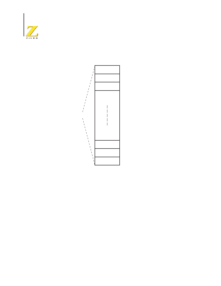
Program Memory
P R E L I M I N A R Y
PS024604-1005
Z8 Encore!
�
Motor Control Flash MCUs
Product Specification
212
Information Area
Table 115 describes the Z8FMC16100 Series Flash MCU's information area. This 512-
byte information area is accessed by setting bit 7 of the Page Select Register to 1. When
access is enabled, the information area is mapped into Program Memory and overlays the
512 bytes at addresses
FE00h
to
FFFFh
. When information area access is enabled, LDC
instructions return data from the information area. CPU instruction fetches always arrive
from Program Memory regardless of the information area access bit. Access to the infor-
mation area is Read-Only.
Figure 39. Flash Memory Arrangement
16KB Flash
Program Memory
01FFh
0200h
03FFh
05FFh
0400h
0000h
3BFFh
3C00h
3DFFh
3FFFh
3E00h
3A00h
32 Pages
512 Bytes per Page

PS024604-1005
P R E L I M I N A R Y Operation
Z8FMC16100 Series Flash MCU
Product Specification
213
Operation
The Flash Controller provides the proper signals and timing for the Byte Programming,
Page Erase, and Mass Erase operations in Flash memory. The Flash Controller contains a
protection mechanism, via the Flash Control Register (FCTL), to prevent accidental pro-
gramming or erasure. The following subsections provide details about the Lock, Unlock,
Sector Protect, Byte Programming, Page Erase, and Mass Erase operations.
Timing Using the Flash Frequency Registers
Before performing a program or erase operation on Flash memory, the user must first con-
figure the Flash Frequency High and Low Byte registers. The Flash Frequency registers
allow programming and erasure of Flash with system clock frequencies ranging from
32 KHz through 20 MHz (the valid range is limited to device operating frequencies).
The Flash Frequency High and Low Byte registers combine to form a 16-bit value,
FFREQ
, to control the timing of Flash program and erase operations. The 16-bit Flash Fre-
quency value must contain the system clock frequency in kilohertz. This value is calcu-
lated using the following equation:
Flash programming and erasure are not supported for system clock frequencies below
32 KHz, above 20 MHz, or outside of the device's operating frequency range. The Flash
Frequency High and Low Byte registers must be loaded with the correct value to ensure
proper Flash programming and erase operations.
Flash Read Protection
The user code contained within Flash memory can be protected from external access. Pro-
gramming the Flash Read Protect option bit prevents the reading of user code by the On-
Table 115. Z8FMC16100 Series Flash MCU Information Area Map
Program Memory
Address (Hex)
Function
FE00h�FE3Fh
Reserved.
FE40h�FE53h
Part Number:20-character ASCII alphanumeric
code, left-justified and filled with zeroes.
FE54h�FFFFh
Reserved.
FFREQ[15:0] =
System Clock Frequency (Hz)
1000
Caution:

Program Memory
P R E L I M I N A R Y
PS024604-1005
Z8 Encore!
�
Motor Control Flash MCUs
Product Specification
214
Chip Debugger or by using the Flash Controller Bypass mode. Refer to the
Option Bits
chapter on page 223 and the
On-Chip Debugger
chapter on page 241 for more informa-
tion.
Flash Write/Erase Protection
The Z8FMC16100 Series Flash MCU device provides several levels of protection against
accidental program and erasure of the contents of Flash memory. This protection is pro-
vided by the Flash Controller unlock mechanism, the Flash Sector Protect Register, and
the Flash Write Protect option bit.
Flash Controller Unlock Mechanism
At Reset, the Flash Controller locks to prevent accidental program or erasure of Flash
memory. To program or erase Flash memory, the Flash Controller must be unlocked. After
unlocking the Flash Controller, the Flash can be programmed or erased. Any value written
by user code to the Flash Control Register or Page Select Register out of sequence will
lock the Flash Controller.
The proper steps to unlock the Flash Controller from user code are:
1. Write
00h
to the Flash Control Register to reset the Flash Controller.
2. Write the page to be programmed or erased to the Page Select Register.
3. Write the first unlock command
73h
to the Flash Control Register.
4. Write the second unlock command
8Ch
to the Flash Control Register.
5. Rewrite the page written in Step 2 to the Page Select Register.
Flash Sector Protection
The Flash Sector Protect Register can be configured to prevent sectors from being pro-
grammed or erased. After a sector is protected, it cannot be unprotected by user code. The
Flash Sector Protect Register is cleared after reset and any previously written protection
values are lost. User code must write this register in their initialization routine if they want
to enable sector protection.
The Flash Sector Protect Register shares its Register File address with the Page Select
Register. The Flash Sector Protect Register is accessed by writing the Flash Control Regis-
ter with
5EH
. After the Flash Sector Protect Register is selected, it can be accessed at the
Page Select Register address. When user code writes the Flash Sector Protect Register,
bits can only be set to 1. Therefore, sectors can be protected, but not unprotected, via reg-
ister Write operations. The Flash Sector Protect Register is deselected by writing any
value to the Flash Control Register.
The steps to setup the Flash Sector Protect Register from user code are:
1. Write
00h
to the Flash Control Register to reset the Flash Controller.

PS024604-1005
P R E L I M I N A R Y Byte
Programming
Z8FMC16100 Series Flash MCU
Product Specification
215
2. Write
5Eh
to the Flash Control Register to select the Flash Sector Protect Register.
3. Read and/or write the Flash Sector Protect Register, which now resides at Register
File address
FF9h
.
4. Write
00h
to the Flash Control Register to return the Flash Controller to its reset state.
Flash Write Protection Option Bit
The Flash Write Protect option bit can be enabled to block all program and erase opera-
tions from user code. Refer to the
Option Bits
chapter on page 223 for more information.
Byte Programming
When the Flash Controller is unlocked, Writes to Program Memory from user code will
program a byte into the Flash if the address is located in the unlocked page. An erased
Flash byte contains all ones (
FFh
). The programming operation can only be used to
change bits from one to zero. To change a Flash bit (or multiple bits) from zero to one
requires a Page Erase or Mass Erase operation.
Byte programming can be performed using the eZ8 CPU's LDC or LDCI instructions.
Refer to the eZ8 CPU User Manual (UM0128) for a description of the LDC and LDCI
instructions.
While the Flash Controller programs Flash memory, the eZ8 CPU idles, but the system
clock and on-chip peripherals continue to operate. Interrupts that occur when a program-
ming operation is in progress are serviced after the programming operation is complete. To
exit programming mode and lock the Flash Controller, write
00h
to the Flash Control
Register.
User code cannot program Flash Memory on a page that lies in a protected sector. When
user code writes memory locations, only addresses located in the unlocked page are pro-
grammed. Memory Writes outside of the unlocked page are ignored.
Each memory location must not be programmed more than twice before an erase is re-
quired.
The proper steps to program Flash memory from user code are:
1. Write
00h
to the Flash Control Register to reset the Flash Controller.
2. Write the page of memory to be programmed to the Page Select Register.
3. Write the first unlock command
73h
to the Flash Control Register.
4. Write the second unlock command
8Ch
to the Flash Control Register.
5. rewrite the page written in Step 2 to the Page Select Register.
6. Write Program Memory using LDC or LDCI instructions to program Flash.
7. Repeat Step 6 to program additional memory locations on the same page.
Caution:

Program Memory
P R E L I M I N A R Y
PS024604-1005
Z8 Encore!
�
Motor Control Flash MCUs
Product Specification
216
8. Write
00h
to the Flash Control Register to lock the Flash Controller.
Page Erase
Flash memory can be erased one page (512 bytes) at a time. Page-erasing Flash memory
sets all bytes in that page to the value
FFh
. The Page Select Register identifies the page to
be erased. While the Flash Controller executes the Page Erase operation, the eZ8 CPU
idles, but the system clock and on-chip peripherals continue to operate. The eZ8 CPU
resumes operation after the Page Erase operation completes. Interrupts that occur when
the Page Erase operation is in progress are serviced after the Page Erase operation is com-
plete. When the Page Erase operation is complete, the Flash Controller returns to its
locked state. Only pages located in unprotected sectors can be erased.
The proper steps to perform a Page Erase operation are:
1. Write
00h
to the Flash Control Register to reset the Flash Controller.
2. Write the page to be erased to the Page Select Register.
3. Write the first unlock command,
73h
, to the Flash Control Register.
4. Write the second unlock command
8Ch
to the Flash Control Register.
5. Rewrite the page written in Step 2 to the Page Select Register.
6. Write the Page Erase command,
95h
, to the Flash Control Register.
Mass Erase
Flash memory cannot be mass-erased by user code.
Flash Controller Bypass
The Flash Controller can be bypassed and the control signals for Flash memory brought
out to the GPIO pins. Bypassing the Flash Controller allows faster programming algo-
rithms by controlling the Flash programming signals directly.
Flash Controller Bypass is recommended for gang-programming applications and large-
volume customers who do not require in-circuit programming of Flash memory.
Refer to the ZiLOG Application Note titled Third-Party Flash Programming Support for
the Z8 Encore!
�
MCU (AN0117) for more information about bypassing the Flash control-
ler. This document is available for download at
www.zilog.com
.
Flash Controller Behavior in Debug Mode
The following changes in behavior of the Flash Controller occur when the Flash Control-
ler is accessed using the On-Chip Debugger:

PS024604-1005
P R E L I M I N A R Y Flash
Control
Register
Z8FMC16100 Series Flash MCU
Product Specification
217
�
The Flash Write Protect option bit is ignored
�
The Flash Sector Protect Register is ignored for programming and erase operations
�
Programming operations are not limited to the page selected in the Page Select Register
�
Bits in the Flash Sector Protect Register can be written to one or zero
�
The second write of the Page Select Register to unlock the Flash Controller is not nec-
essary
�
The Page Select Register can be written when the Flash Controller is unlocked
�
The Mass Erase command is enabled through the Flash Control Register
�
The page erase and programming operations are disabled if the Memory Read Protect
option is enabled
Flash Control Register
The Flash Control Register, shown in Table 116, unlocks the Flash Controller for pro-
gramming and erase operations, or to select the Flash Sector Protect Register.
The Write-Only Flash Control Register shares its Register File address with the Read-
Only Flash Status Register.
Table 116. Flash Control Register (FCTL)
BITS
7
6
5
4
3
2
1
0
FIELD
FCMD
RESET
00H
R/W
W
ADDR
FF8H
Bit
Position
Value
Description
[7:0]
FCMD
73H
8CH
95H
63H
5EH
Flash Command:
First unlock command.
Second unlock command.
Page erase command.
Mass erase command.
Flash Sector Protect register select.
All other commands, or any command out of sequence, locks the Flash
Controller.

Program Memory
P R E L I M I N A R Y
PS024604-1005
Z8 Encore!
�
Motor Control Flash MCUs
Product Specification
218
Flash Status Register
The Flash Status Register, shown in Table 117, indicates the current state of the Flash Con-
troller. This register can be read at any time. The read-only Flash Status Register shares its
Register File address with the write-only Flash Control Register.
Flash Page Select Register
The Flash Page Select (FPS) Register, shown in Table 118, selects one of the 32 available
Flash memory pages to be erased or programmed. Each Flash Page contains 512 bytes of
Flash memory. During a Page Erase operation, all Flash memory locations with the 7 most
significant bits of the address assigned by the
PAGE
field are erased to
FFh
.
The Flash Page Select Register shares its Register File address with the Flash Sector Pro-
tect Register. The Flash Page Select Register cannot be accessed when the Flash Sector
Protect Register is enabled.
Table 117. Flash Status Register (FSTAT)
BITS
7
6
5
4
3
2
1
0
FIELD
Reserved
FSTAT
RESET
00B
00_0000B
R/W
R
R
ADDR
FF8H
Bit
Position
Value
Description
[7:6]
Reserved
Must be 00.
[5:0]
FSTAT
00_0000
00_0001
00_0010
00_0011
00_0100
00_1xxx
01_0xxx
10_0xxx
Flash Controller Status
Flash Controller locked.
First unlock command received.
Second unlock command received.
Flash Controller unlocked.
Flash Sector Protect register selected.
Program operation in progress.
Page erase operation in progress.
Mass erase operation in progress.
PS024604-1005
P R E L I M I N A R Y
Flash Sector Protect Register
Z8FMC16100 Series Flash MCU
Product Specification
219
Flash Sector Protect Register
The Flash Sector Protect Register, shown in Table 119, protects Flash memory sectors
from being programmed or erased from user code. The Flash Sector Protect Register
shares its Register File address with the Flash Page Select Register. The Flash Sector pro-
tect Register can be accessed only after writing the Flash Control Register with
5Eh
.
User code can only write bits in this register to 1 (bits cannot be cleared to 0 by user code).
Table 118. Flash Page Select Register (FPS)
BITS
7
6
5
4
3
2
1
0
FIELD
INFO_EN
PAGE
RESET
0
000_0000B
R/W
R/W
R/W
ADDR
FF9H
Bit
Position
Value
Description
[7]
INFO_EN
0
Information Area Enable
Information area is not selected.
1
Information Area is selected.
The Information area is mapped into the Program Memory address space at
addresses FE00H through FFFFH.
[6:0]
PAGE
Page Select
This 7-bit field selects the Flash memory page for Programming and Page Erase
operations. Program Memory Address[15:9] = PAGE[6:0].
Table 119. Flash Sector Protect Register (FPROT)
BITS
7
6
5
4
3
2
1
0
FIELD
SECT7
SECT6
SECT5
SECT4
SECT3
SECT2
SECT1
SECT0
RESET
0
0
0
0
0
0
0
0
R/W
R/W1
R/W1
R/W1
R/W1
R/W1
R/W1
R/W1
R/W1
ADDR
FF9H
R/W1 = Register is accessible for Read operations. Register can be written to 1 only (through user code).
Program Memory
P R E L I M I N A R Y
PS024604-1005
Z8 Encore!
�
Motor Control Flash MCUs
Product Specification
220
Flash Frequency High and Low Byte Registers
The Flash Frequency High and Low Byte registers, shown in Tables 120 and 121, com-
bine to form a 16-bit value, FFREQ, to control timing for Flash program and erase opera-
tions. The 16-bit Flash Frequency registers must be written with the system clock
frequency in kilohertz for Program and Erase operations. Calculate the Flash Frequency
value using the following equation:
Flash programming and erasure is not supported for system clock frequencies below
32 KHz, above 20 MHz, or outside of the valid operating frequency range for the device.
The Flash Frequency High and Low Byte registers must be loaded with the correct value
to ensure proper program and erase times.
Bit
Position
Value
Description
[7:0]]
SECTn
0
Sector Protect
Sector n can be programmed or erased from user code.
1
Sector n is protected and cannot be programmed or erased from user code.
FFREQ[15:0] = {FFREQH[7:0],FFREQL[7:0]} =
System Clock Frequency
1000
Table 120. Flash Frequency High Byte Register (FFREQH)
BITS
7
6
5
4
3
2
1
0
FIELD
FFREQH
RESET
00H
R/W
R/W
ADDR
FFAH
Caution:
PS024604-1005
P R E L I M I N A R Y Flash Frequency High and Low Byte Registers
Z8FMC16100 Series Flash MCU
Product Specification
221
.
FFREQH and FFREQL--Flash Frequency High and Low Bytes
These 2 bytes, {FFREQH[7:0], FFREQL[7:0]}, contain the 16-bit Flash Frequency value.
Table 121. Flash Frequency Low Byte Register (FFREQL)
BITS
7
6
5
4
3
2
1
0
FIELD
FFREQL
RESET
00H
R/W
R/W
ADDR
FFBH

Program Memory
P R E L I M I N A R Y
PS024604-1005
Z8 Encore!
�
Motor Control Flash MCUs
Product Specification
222

PS024604-1005
P R E L I M I N A R Y Option
Bit
Types
Z8FMC16100 Series Flash MCU
Product Specification
223
Option Bits
Option bits allow user configuration of certain aspects of the Z8FMC16100 Series Flash
MCU operation. The feature configuration data is stored in program memory and read
during Reset. The features available for control using the option bits are:
�
Watch-Dog Timer time-out selection of interrupt or Reset
�
Watch-Dog Timer enabled at Reset
�
Code protection by preventing external read access of program memory
�
The ability to prevent accidental programming and erasure of program memory
�
Voltage Brown-Out can be disabled during STOP mode to reduce power consumption
�
External oscillator mode selection
�
Selectable PWM OFF state, output polarity, fault state, and Reset state
�
Disable PWM output pairs, enabling them as inputs
�
RESET/Fault0 pin function selection
�
Low power clock divide mode selection
Option Bit Types
Two types of option bits, user option bits and trim option bits, allow configuration of cer-
tain aspects of Z8FMC16100 Series Flash MCU operation. Each is described in this sec-
tion.
User Option Bits
The user option bits are contained in the first two bytes of program memory. Because
these locations contain application-specific device configuration, it is possible for the user
to alter these bytes by programming Flash memory.
The information contained in these bytes is lost when page 0 of program memory is
erased.
Trim Option Bits
The trim option bits are contained in the information page of Flash memory. These bits are
factory-programmed values required to optimize the operation of on-board analog cir-
cuitry, and cannot be altered by the user. Program memory can be erased without endan-
gering these values.
Note:
Option Bits
P R E L I M I N A R Y
PS024604-1005
Z8 Encore!
�
Motor Control Flash MCUs
Product Specification
224
It is possible to alter the working values of these bits by accessing the Trim Bit Address
and Data registers, but these working values are lost after a Reset.
There are 32 trim addresses. To read or write these values, the user code must first write a
value between
00h
and
1Fh
into the Trim Bit Address Register. Writing the Trim Bit Data
Register changes the working value of the target trim data. Reading the Trim Bit Data
Register returns the working value of the target trim data.
User Option Bit Configuration By Reset
Each time the user option bits are programmed or erased, the device must be Reset for the
change to take place.
Option Bit Address Space
The first two bytes of program memory at addresses
0000h
, shown in Table 122, and
0001h
, shown in Table 123, are reserved for the user option bits.
Program Memory Address 0000H
Table 122. User Option Bits at Program Memory Address 0000H
BITS
7
6
5
4
3
2
1
0
FIELD WDT_RES WDT_AO
OSC_SEL[1:0]
VBO_AO
RP
Reserved
FWP
RESET
U
U
U
U
U
U
U
R/W
R/W
R/W
R/W
R/W
R/W
R/W
R/W
ADDR
Program Memory 0000H
Note: U = Unchanged by Reset. R/W = Read/Write.
Bit
Position
Value
(H)
Description
[7]
WDT_RES
0
Watch-Dog Timer Reset
Watch-Dog Timer time-out generates an interrupt request. Interrupts must be
globally enabled for the eZ8 CPU to acknowledge the interrupt request.
1
Watch-Dog Timer time-out causes a Reset.
[6]
WDT_AO
0
Watch-Dog Timer Always On
Watch-Dog Timer is automatically enabled.
1
Watch-Dog Timer is enabled upon execution of the WDT instruction.
Caution:

PS024604-1005
P R E L I M I N A R Y
Program Memory Address 0001H
Z8FMC16100 Series Flash MCU
Product Specification
225
Program Memory Address 0001H
These bits define the behavior of the Pulse-Width Modulator. The high and low default
off-state (the output polarity) is also defined here. The off-state is used by the PWM output
control and PWM Fault logic. PWM output pairs can be disabled and used as high-imped-
ance input pins. The RESET/Fault0 pin function is also selectable.
[5:4]
OSC_SEL
00
01
10
11
External Oscillator Mode Selection:
Reserved.
Minimum power for use with very low frequency crystals (32KHz to 1.0MHz).
Medium power for use with medium frequency crystals or ceramic resonators
(0.5MHz to 10.0MHz).
Maximum power for use with high frequency crystals (8.0MHz to 20.0MHz).
[3]
VBO_AO
0
Voltage Brown Out Always On
Voltage Brown-Out Protection is disabled in STOP mode to reduce total power
consumption.
1
Voltage Brown-Out Protection is always enabled.
[2]
RP
0
Read Protect
External access to User program code is disabled.
1
User program code is accessible.
[1]
Reserved
Must be 1.
T
his Option Bit is reserved for future use and must always be 1.
[0]
FWP
0
Flash Write Protect
Programming, Page Erase, and Mass Erase using User Code is disabled.
1
Programming, Page Erase, and Mass Erase are enabled for all of Flash Program
Memory.
Table 123. Options Bits at Program Memory Address 0001H
BITS
7
6
5
4
3
2
1
0
FIELD
FLTSEL
LPDEN
Reserved PWM2EN PWM1EN PWM0EN
PWMHI
PWMLO
RESET
U
U
U
U
U
U
U
U
R/W
R/W
R/W
R/W
R/W
R/W
R/W
R/W
R/W
ADDR
Program Memory 0001H
Note: U = Unchanged by Reset. R/W = Read/Write.
Bit
Position
Value
(H)
Description

Option Bits
P R E L I M I N A R Y
PS024604-1005
Z8 Encore!
�
Motor Control Flash MCUs
Product Specification
226
Bit
Position
Value
(H)
Description
[7]
FLTSEL
0
RESET/Fault0 Select
RESET/Fault0 pin is configured as Fault0 input.
1
RESET/Fault0 pin is configured as RESET input.
[6]
LPDEN
0
Low Power Divide Mode Enable. See
Oscillator Control
chapter on page 231.
Low Power Divide mode is enabled
1
Low Power Divide mode is disabled
[5]
Reserved
Must be 1.
T
his Option Bit is reserved for future use and must always be 1.
[4]
PWM2EN
0
PWM Output Pair PWM2 Enable
PWM2 outputs are enabled and controlled by PWM logic.
1
PWM2 outputs are always high-impedance.
[3]
PWM1EN
0
PWM Output Pair PWM1 Enable
PWM1 outputs are enabled and controlled by PWM logic.
1
PWM1 outputs are always high-impedance.
[2]
PWM0EN
0
PWM Output Pair PWM0 Enable
PWM0 outputs are enabled and controlled by PWM logic.
1
PWM0 outputs are always high-impedance.
[1]
PWMHI
0
PWM High Side (PWM outputs 0H,1H, 2H) Default Off-State
PWM High-side inactive state is low, active state is High.
1
PWM High-side inactive state is high, active state is Low.
[0]
PWMLO
0
PWM Low Side (PWM outputs 0L,1L, 2L) Default Off-State
PWM Low-side inactive state is low, active state is high.
1
PWM Low-side inactive state is high, active state is low.

PS024604-1005
P R E L I M I N A R Y
Trim Bit Address Register
Z8FMC16100 Series Flash MCU
Product Specification
227
Trim Bit Address Register
The Trim Bit Address Register, shown in Table 124, contains the target address for access
to the trim option bits.
Trim Bit Data Register
Trim Bit Data Register, shown in Table 125, contains the read or write data for access to
addresses in the Trim Bit Address Register.
Table 124. Trim Bit Address Register (TRMADR)
BITS
7
6
5
4
3
2
1
0
FIELD
TRMADR
RESET
00H
R/W
R/W
ADDR
FF6H
Bit Position Value (H) Description
[7:0}
TRMADR
00 - 1FH Trim Bit Address Register
Table 125. Trim Bit Data Register (TRMDR)
BITS
7
6
5
4
3
2
1
0
FIELD
TRMDR
RESET
00H
R/W
R/W
ADDR
FF7H
Bit Position Value (H) Description
[7:0}
TRMDR
00 - FFH Trim Bit Data Register

Option Bits
P R E L I M I N A R Y
PS024604-1005
Z8 Encore!
�
Motor Control Flash MCUs
Product Specification
228
Trim Bit Address 0001H
This register is loaded from the Flash Information Area following reset or STOP mode
recovery. Writing to this register allows user frequency adjustment of the IPO. Writing to
this register does not effect the Flash memory contents.
Trim Bit Address 0002H
This register is loaded from the Flash Information Area following reset or STOP mode
recovery. Writing to this register allows user frequency adjustment of the IPO. Writing to
this register does not effect the Flash memory contents.
Table 126. IPO Trim Option Bits at 0001H (IPO_TRIM)
BITS
7
6
5
4
3
2
1
0
FIELD
TEMP_TRIM
IPO_TRIM[9:8]
RESET
U
R/W
R/W
ADDR
Information Page Memory 0021H
U = Unchanged by Reset. R/W = Read/Write.
Bit Position Value (H) Description
TEMP_TRIM
[5:0]
00 - 3FH Internal precision Oscillator trim bits for Temperature compensation.
IPO_TRIM
[9:8]
00 - 11H
Internal Precision Oscillator Trim Byte
Used with IPO Trim1 options bits as bits [9:8]. Trimming for Internal Precision
Oscillator frequency adjustment.
Table 127. IPO Trim1 Option Bits at 0002H (IPO_TRIM1)
BITS
7
6
5
4
3
2
1
0
FIELD
IPO_TRIM[7:0]
RESET
U
R/W
R/W
ADDR
Information Page Memory 0022H
U = Unchanged by Reset. R/W = Read/Write.

PS024604-1005
P R E L I M I N A R Y
Trim Bit Address 0003H
Z8FMC16100 Series Flash MCU
Product Specification
229
Trim Bit Address 0003H
Vref_TRIM--Trim values for the Vref circuit used by the Analog to Digital Converter
Contains factory trimmed values for Vref (ADC Reference Voltage) These values are used
to set the Vref voltage to meet specified tolerance. The format is TBD.
Bit Position Value (H) Description
IPO_TRIM
[7:0]
00 - FFH Internal Precision Oscillator Trim Byte
Trimming byte for Internal Precision Oscillator frequency adjustment. Use with
IPO trim bits [9:8} in previous register
Table 128. Trim Option Bits at 0004H (ADCCAL)
BITS
7
6
5
4
3
2
1
0
FIELD
Reserved
Vref_TRIM
RESET
U
R/W
R/W
ADDR
Information Page Memory 0023H
Note: U = Unchanged by Reset. R/W = Read/Write.

Option Bits
P R E L I M I N A R Y
PS024604-1005
Z8 Encore!
�
Motor Control Flash MCUs
Product Specification
230

PS024604-1005
P R E L I M I N A R Y Operation
Z8FMC16100 Series Flash MCU
Product Specification
231
Oscillator Control
The Z8FMC16100 Series Flash MCU uses three possible clocking schemes, each user-
selectable:
�
Trimmable Internal Precision Oscillator
�
On-chip oscillator using off-chip crystal/resonator or external clock driver
�
On-chip low precision Watch-Dog Timer oscillator
In addition, Z8FMC16100 Series Flash MCUs contain clock failure detection and recov-
ery circuitry, allowing continued operation despite any potential failure of the primary
oscillator.
The on-chip system clock frequency can be reduced via a clock divider allowing reduced
dynamic power dissipation. Flash memory can be powered down during portions of the
clock period when running slower than 10 MHz.
Operation
This section explains the logic used to select the system clock, divide down the system
clock, and handle oscillator failures. A description of the specific operation of each oscil-
lator is outlined elsewhere in this document. Refer to
Watch-Dog Timer
chapter on page
63, the
On-Chip Oscillator
chapter on page 237, and the
Internal Precision Oscillator
chapter on page 239.
System Clock Selection
The oscillator control block selects from the available clocks. Table 129 details each clock
source and its usage.

Oscillator Control
P R E L I M I N A R Y
PS024604-1005
Z8 Encore!
�
Motor Control Flash MCUs
Product Specification
232
Unintentional accesses to the Oscillator Control Register (OSCCTL) can stop the chip by
switching to a nonfunctioning oscillator. Accidental alteration of the OSCCTL register is
prevented by a locking/unlocking scheme. To write the register, unlock it by making two
writes to the OSCCTL register with the values
E7H
followed by
18H
. A third write to the
OSCCTL register then changes the value of the register and returns the register to a locked
state. Any other sequence of oscillator control register writes has no effect. The values
written to unlock the register must be ordered correctly, but need not be consecutive. It is
possible to access other registers within the locking/unlocking operation.
Clock Selection Following System Reset
The Internal Precision Oscillator is selected following a System Reset. Startup code after
the System Reset may change the system clock source by unlocking and configuring the
OSCCTL register. If the
LPDEN
bit in Program Memory Address 0001H is zero, Flash
Low Power mode is enabled during reset. When Flash Low Power mode is enabled during
reset, the
FLPEN
bit in the Oscillator Control Register (OSCCTL) will be set and the
DIV
field of the OSCDIV register will be set to
08h
.
Clock Failure Detection and Recovery for Primary Oscillator
The Z8FMC16100 Series Flash MCU generates a System Exception when a failure of the
primary oscillator occurs if the
POFEN
bit is set in the OSCCTL Register. To maintain sys-
tem function in this situation, the clock failure recovery circuitry automatically forces the
Table 129. Oscillator Configuration and Selection
Clock Source
Characteristics
Required Setup
Internal Precision
Oscillator
� 5.5296 MHz
� High precision possible when trimmed
� No external components required
� This is the reset default.
External Crystal/
Resonator/
External Clock
Drive
� 0 to 20MHz
� Very high accuracy (dependent on
crystal/resonator or external source)
� Requires external components
� Configure Option Bits for correct
external oscillator mode
� Unlock and write Oscillator Control
Register (OSCCTL) to enable external
oscillator
� Wait for required stabilization time
� Unlock and write Oscillator Control
Register (OSCCTL) to select external
oscillator
Internal Watchdog
Timer Oscillator
� 10KHz nominal
� Low accuracy
� No external components required
� Low power consumption
� Unlock and write Oscillator Control
Register (OSCCTL) to enable and select
Internal WDT oscillator

PS024604-1005
P R E L I M I N A R Y Clock Failure Detection and Recovery for WDT
Z8FMC16100 Series Flash MCU
Product Specification
233
Watch-Dog Timer oscillator to drive the system clock. Although this oscillator runs at a
much lower frequency than the original system clock, the CPU continues to operate,
allowing execution of a clock failure vector and software routines that either remedy the
oscillator failure or issue a failure alert. This automatic switch-over is not available if the
Watch-Dog Timer is the primary oscillator.
The primary oscillator failure detection circuitry asserts if the system clock frequency
drops below 1KHz �+/-50%. For operating frequencies below 2KHz, do not enable the
clock failure circuitry (
POFEN
must be deasserted in the OSCCTL register).
Clock Failure Detection and Recovery for WDT Oscillator
In the event of a Watch-Dog Timer oscillator failure, a System Exception will be issued if
the
WDFEN
bit of the OSCCTL register is set. This event does not trigger an attendant clock
switch-over, but alerts the CPU of the failure. After a Watch-Dog Timer failure, it is no
longer possible to detect a primary oscillator failure.
The Watch-Dog Timer oscillator failure detection circuit counts system clocks while look-
ing for a Watch-Dog Timer clock. The logic counts 8000 system clock cycles before deter-
mining that a failure occurred. The system clock rate determines the speed at which the
Watch-Dog Timer failure can be detected. A very slow system clock results in very slow
detection times. If the Watch-Dog Timer is the primary oscillator or if the Watch-Dog
Timer oscillator is disabled, deassert the
WDFEN
bit of the OSCCTL register.
Oscillator Control Register
The Oscillator Control Register (OSCCTL) enables/disables the various oscillator circuits,
enables/disables the failure detection/recovery circuitry, actively powers down the flash,
and selects the primary oscillator, which becomes the system clock.
The Oscillator Control Register must be unlocked before writing. Writing the two-step
sequence
E7H
followed by
18H
to the Oscillator Control Register address unlocks it. The
register locks after completion of a register write to the OSCCTL.
Table 130. Oscillator Control Register (OSCCTL)
BITS
7
6
5
4
3
2
1
0
FIELD
INTEN
XTLEN
WDTEN
POFEN
WDFEN
FLPEN
SCKSEL
RESET
1
0
1
0
0
0*
00
R/W
R/W
R/W
R/W
R/W
R/W
R/W
R/W
ADDR
F86H
* The reset value is 1 if the option bit LPDEN is 0.

Oscillator Control
P R E L I M I N A R Y
PS024604-1005
Z8 Encore!
�
Motor Control Flash MCUs
Product Specification
234
Oscillator Divide Register
The Oscillator Divide Register (OSCDIV) provides the value that divides the system
clock. The Oscillator Divide Register must be unlocked before writing. Writing the two-
step sequence
E7h,
followed by
18h
, to the Oscillator Control Register address unlocks
the register. The register locks after completion of a register Write to the OSCDIV.
Bit
Position
Value
(H)
Description
[7]
INTEN
0
Internal Precision Oscillator Enable
Internal precision oscillator is disabled.
1
Internal precision oscillator is enabled.
[6]
XTLEN
0
Crystal Oscillator Enable
Crystal oscillator is disabled.
1
Crystal oscillator is enabled.
[5]
WDTEN
0
Watch-Dog Timer Oscillator Enable
Watch-Dog Timer oscillator is disabled
1
Watch-Dog Timer oscillator is enabled
[4]
POFEN
0
Primary Oscillator Failure Detection Enable
Failure detection and recovery of primary oscillator is disabled. This bit is cleared
automatically if a primary oscillator failure is detected.
1
Failure detection and recovery of primary oscillator is enabled
[3]
WDFEN
0
Watch-Dog Timer Oscillator Failure Detection Enable
Failure detection of Watch-Dog Timer oscillator is disabled.This bit is cleared
automatically if a Watch-Dog Timer oscillator failure is detected.
1
Failure detection of Watch-Dog Timer oscillator is enabled
[2]
FLPEN
0
Flash Low Power Mode Enable
Flash Low Power Mode is disabled.
1
Flash Low Power Mode is enabled. The Flash will be powered down during idle
periods of the clock and powered up during Flash reads. This bit should only be
set if the frequency of the primary oscillator source is 8MHz or lower. The reset
value of this bit is controlled by the LPDEN option bit during reset.
[1:0]
SCKSEL
00
01
10
11
System Clock Oscillator Select
Internal precision oscillator functions as system clock at 5.6 MHz
Crystal oscillator or external clock driver functions as system clock
Reserved
Watch-Dog Timer oscillator functions as system clock

PS024604-1005
P R E L I M I N A R Y Oscillator
Divide
Register
Z8FMC16100 Series Flash MCU
Product Specification
235
Table 131. Oscillator Divide Register (OSCDIV)
BITS
7
6
5
4
3
2
1
0
FIELD
DIV
RESET
00H*
R/W
R/W
ADDR
F87H
* The reset value is 08H if the option bit LPDEN is 0.
Bit
Position
Value
(H)
Description
[7:0]
DIV
00H to
FFH
Oscillator Divide
00H - divider is disabled, all other entries are the divide value for scaling the
system clock.

Oscillator Control
P R E L I M I N A R Y
PS024604-1005
Z8 Encore!
�
Motor Control Flash MCUs
Product Specification
236
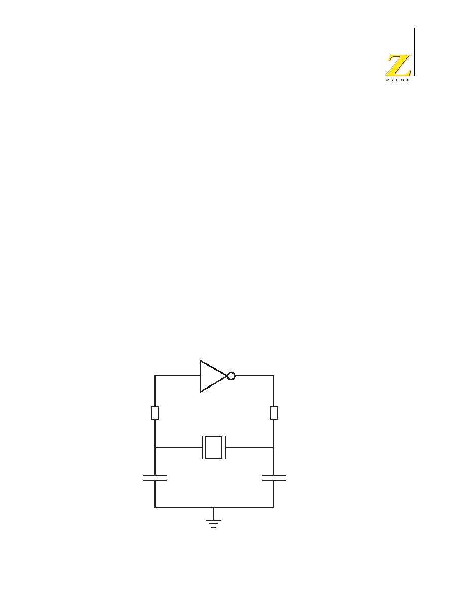
PS024604-1005
P R E L I M I N A R Y Crystal
Oscillator
Operation
Z8FMC16100 Series Flash MCU
Product Specification
237
On-Chip Oscillator
The products in the Z8FMC16100 Series Flash MCU features an on-chip oscillator for use
with external crystals with frequencies ranging from 32 KHz to 20 MHz. In addition, the
oscillator can support ceramic resonators with oscillation frequencies up to 20 MHz. This
oscillator generates the primary system clock for the internal eZ8 CPU and the majority of
the on-chip peripherals. Alternatively, the X
IN
input pin can also accept a CMOS-level
clock input signal (32 KHz�20 MHz). If an external clock generator is used, the X
OUT
pin
must remain unconnected.
When configured for use with crystal oscillators or external clock drivers, the frequency of
the signal on the X
IN
input pin determines the frequency of the system clock (that is, no
internal clock divider).
Crystal Oscillator Operation
Figure 40 illustrates a recommended configuration for connection with an external funda-
mental-mode, parallel-resonant crystal operating at 20 MHz. Recommended 20 MHz crys-
tal specifications are provided in Table 132. The printed circuit board layout must add no
more than 4 pF of stray capacitance to either the X
IN
or X
OUT
pins. If oscillation does not
occur, reduce the values of capacitors C1 and C2 to decrease loading.
Figure 40. Recommended 20MHz Crystal Oscillator Configuration
X
C = 22 pF
IN
X
OUT
2
C = 22 pF
2
20 MHz Crystal
(Fundamental Mode)
On-Chip Oscillator

On-Chip Oscillator
P R E L I M I N A R Y
PS024604-1005
Z8 Encore!
�
Motor Control Flash MCUs
Product Specification
238
Table 132. Recommended Crystal Oscillator Specifications (20MHz Operation)
Parameter
Value
Units
Comments
Frequency
20
MHz
Resonance
Parallel
Mode
Fundamental
Series Resistance (R
S
)
25
Ohm
Maximum
Load Capacitance (C
L
)
20
pF
Maximum
Shunt Capacitance (C
0
)
7
pF
Maximum
Drive Level
1
mW
Minimum

PS024604-1005
P R E L I M I N A R Y Operation
Z8FMC16100 Series Flash MCU
Product Specification
239
Internal Precision Oscillator
The Internal Precision Oscillator (IPO) is designed for use without external components.
The IPO comes factory trimmed a �4% frequency accuracy over the operating tempera-
ture and supply voltage range of the device. IPO features include:
�
On-chip RC oscillator that does not require external components
�
Trimmed to �4% accuracy
�
Target output frequency of 5.5296 MHz
�
Trimming possible through Flash option bits with user override
�
Can eliminate crystals or ceramic resonators in applications where high timing accura-
cy is not required.
Operation
The internal oscillator is an RC relaxation oscillator that has had its sensitivity to power
supply variation minimized. By using ratio tracking thresholds, the effect of power supply
voltage is cancelled out. The dominant source of oscillator error is the absolute variance of
chip-level fabricated components, such as capacitors. Two 8-bit trimming registers, incor-
porated into the design, allow compensation of absolute variation of oscillator frequency.
Once calibrated, the oscillator frequency is relatively stable and does not require subse-
quent calibration.
By default, the oscillator is configured through the Flash Option bits. However, the user
code can override these trim values as described in
Trim Option Bits
section on page 223.

Internal Precision Oscillator
P R E L I M I N A R Y
PS024604-1005
Z8 Encore!
�
Motor Control Flash MCUs
Product Specification
240

PS024604-1005
P R E L I M I N A R Y Architecture
Z8FMC16100 Series Flash MCU
Product Specification
241
On-Chip Debugger
The Z8FMC16100 Series Flash MCU device includes an integrated On-Chip Debugger
(OCD) that provides advanced debugging features, including:
�
Reading and writing of the Register File
�
Reading and writing of program and data memory
�
Setting of break points
�
Execution of eZ8 CPU instructions
Architecture
The On-Chip Debugger consists of four primary functional blocks: Transmitter, Receiver,
Autobaud Generator, and Debug Controller. Figure 41 illustrates the architecture of the
On-Chip Debugger.
OCD Interface
The On-Chip Debugger (OCD) uses the DBG pin for communication with an external
host. This one-pin interface is a bidirectional open-drain interface that transmits and
Figure 41. On-Chip Debugger Block Diagram
Autobaud
Detector/Generator
System
Clock
DBG Pin
Transmitter
Debug Controller
eZ8 CPU
Control
Receiver

On-Chip Debugger
P R E L I M I N A R Y
PS024604-1005
Z8 Encore!
�
Motor Control Flash MCUs
Product Specification
242
receives data. Data transmission is half-duplex, in that transmit and receive cannot occur
simultaneously. The serial data on the DBG pin is sent using the standard asynchronous
data format defined in RS-232. This pin interfaces the Z8FMC16100 Series Flash MCU
device to the serial port of a host PC using minimal external hardware. Two different
methods for connecting the DBG pin to an RS-232 interface are depicted in Figures 42
and 43 .
For operation of the Z8FMC16100 Series Flash MCU, all power pins (V
DD
and AV
DD
)
must be supplied with power, and all ground pins (V
SS
and AV
SS
) must be properly
grounded. The DBG pin should always be connected to V
DD
through an external pull-
up resistor.
Figure 42. Interfacing the On-Chip Debugger's DBG Pin with an RS-232 Interface (1)
Figure 43. Interfacing the On-Chip Debugger's DBG Pin with an RS-232 Interface (2)
Caution:
V
DD
Diode
RS-232
Transceiver
DBG pin
10K
RS232 TX
RS232 RX
V
DD
Open-Drain
Buffer
RS-232
Transceiver
DBG pin
10K
RS232 TX
RS232 RX

PS024604-1005
P R E L I M I N A R Y Debug
Mode
Z8FMC16100 Series Flash MCU
Product Specification
243
Debug Mode
The operating characteristics of the Z8FMC16100 Series Flash MCU device in DEBUG
mode are:
�
The eZ8 CPU fetch unit stops, idling the eZ8 CPU, unless directed by the OCD to ex-
ecute specific instructions
�
The system clock operates unless in STOP mode
�
All enabled on-chip peripherals operate unless in STOP mode or otherwise defined by
the on-chip peripheral to disable in DEBUG mode
�
Automatically exits HALT mode
�
Constantly refreshes the Watch-Dog Timer, if enabled
Entering Debug Mode
The device enters DEBUG mode following any of the following operations:
�
Writing the DBGMODE bit in the OCD Control Register to 1 using the OCD interface
�
eZ8 CPU execution of a BRK (break point) instruction (when enabled)
�
Match of PC to OCDCNTR register (when enabled)
�
OCDCNTR register decrements to
0000h
(when enabled)
�
The DBG pin is Low when the device exits Reset
Exiting Debug Mode
The device exits DEBUG mode following any of the following operations:
�
Clearing the DBGMODE bit in the OCD Control Register to 0
�
Power-on reset
�
Voltage Brown Out reset
�
Asserting the RESET pin Low to initiate a Reset
�
Driving the DBG pin Low while the device is in STOP mode initiates a System Reset
OCD Data Format
The On-Chip Debugger (OCD) interface uses the asynchronous data format defined for
RS-232. Each character is transmitted as 1 start bit, 8 data bits (least-significant bit first),
and 1 stop bit. See Figure 44.

On-Chip Debugger
P R E L I M I N A R Y
PS024604-1005
Z8 Encore!
�
Motor Control Flash MCUs
Product Specification
244
OCD Auto-Baud Detector/Generator
To run over a range of baud rates (bits per second) with various system clock frequencies,
the On-Chip Debugger has an Auto-Baud Detector/Generator. After a reset, the OCD is
idle until it receives data. The OCD requires that the first character sent from the host is
the character
80h
. The character
80h
contains eight continuous bits Low (one Start bit
plus 7 data bits). The Auto-Baud Detector measures this period and sets the OCD Baud
Rate Generator accordingly.
The Auto-Baud Detector/Generator is clocked by the system clock. The minimum baud
rate is the system clock frequency divided by 512. The maximum recommended baud rate
is the system clock frequency divided by 8. Table 133 lists minimum and recommended
maximum baud rates for sample crystal frequencies.
If the OCD receives a Serial Break (ten or more continuous bits Low) the Auto-Baud
Detector/Generator resets. The Auto-Baud Detector/Generator can then be reconfigured
by sending
80h
. If the Auto-Baud Detector overflows while measuring the Auto-Baud
character, the Auto-Baud Detector will remain reset.
OCD Serial Errors
The On-Chip Debugger can detect any of the following error conditions on the DBG pin:
�
Serial Break (a minimum of ten continuous bits Low)
�
Framing Error (received STOP bit is Low)
Figure 44. OCD Data Format
Table 133. OCD Baud-Rate Limits
System Clock
Frequency
Maximum Asynchronous
Baud Rate (bits/s)
Minimum
Baud Rate (bits/s)
20.0 MHz
2.5 M
39.1 K
1.0 MHz
125 K
1960
32.768 KHz
4096
64
ST
ST = Start Bit
SP = Stop Bit
D0--D7 = Data Bits
D0
D1
D2
D3
D4
D5
D6
D7
SP

PS024604-1005
P R E L I M I N A R Y Automatic
Reset
Z8FMC16100 Series Flash MCU
Product Specification
245
�
Transmit Collision (OCD and host simultaneous transmission detected by the OCD)
When the OCD detects one of these errors, it aborts any command currently in progress,
transmits a Serial Break 4096 system clock cycles long back to the host, and resets the
Auto-Baud Detector/Generator. A Framing Error or Transmit Collision can be caused by
the host sending a Serial Break to the OCD. Because of the open-drain nature of the inter-
face, returning a Serial Break break back to the host only extends the length of the Serial
Break if the host releases the Serial Break early.
The host transmits a Serial Break on the DBG pin when first connecting to the
Z8FMC16100 Series Flash MCU device or when recovering from an error. A Serial Break
from the host resets the Auto-Baud Generator/Detector but does not reset the OCD Con-
trol Register. A Serial Break leaves the device in DEBUG mode if that is the current mode.
The OCD is held in Reset until the end of the Serial Break when the DBG pin returns
High. Because of the open-drain nature of the DBG pin, the host can send a Serial Break to
the OCD even if the OCD is transmitting a character.
Automatic Reset
The Z8FMC16100 Series Flash MCU devices have the capability to switch clock sources
during operation. If the Auto-Baud is set and the clock source is switched, the Auto-Baud
value becomes invalid. A new Auto-Baud value must be configured with the new clock
frequency.
The oscillator control logic has clock switch detection. If a clock switch is detected and
the Auto-Baud is set, the device will automatically send a Serial Break for 4096 clocks.
This will reset the Auto-Baud and indicate to the host that a new Auto-Baud character
should be sent.
Break Points
Execution break points are generated using the BRK instruction (Op Code
00h
). When the
eZ8 CPU decodes a BRK instruction, it signals the On-Chip Debugger. If break points are
enabled, the OCD idles the eZ8 CPU and enters DEBUG mode. If break points are not
enabled, the OCD ignores the BRK signal and the BRK instruction operates as a NOP
instruction.
If break points are enabled, the OCD can be configured to automatically enter DEBUG
mode, or to loop on the break instruction. If the OCD is configured to loop on the BRK
instruction, then the CPU remains able to service DMA and interrupt requests.
The loop on BRK instruction can service interrupts in the background. For interrupts to be
serviced in the background, there cannot be any break points in the interrupt service rou-
tine. Otherwise, the CPU stops on the break point in the interrupt routine. For interrupts to
be serviced in the background, interrupts must also be enabled. Debugging software does
not automatically enable interrupts when using this feature. Interrupts are typically dis-

On-Chip Debugger
P R E L I M I N A R Y
PS024604-1005
Z8 Encore!
�
Motor Control Flash MCUs
Product Specification
246
abled during critical sections of code where interrupts do not occur (such as adjusting the
stack pointer or modifying shared data).
Host software can poll the IDLE bit of the OCDSTAT register to determine if the OCD is
looping on a BRK instruction. When software wants to stop the CPU on the BRK instruc-
tion on which it is looping, software must not set the DBGMODE bit of the OCDCTL reg-
ister. The CPU may have vectored to an interrupt service routine. Instead, software clears
the BRKLP bit. This allows the CPU to finish the interrupt service routine it may be in and
return to the BRK instruction. When the CPU returns to the BRK instruction on which it
was previously looping, it automatically sets the DBGMODE bit and enters DEBUG
mode.
The majority of the OCD commands remain disabled when the eZ8 CPU is looping on a
BRK instruction. The eZ8 CPU must be in DEBUG mode before these commands can be
issued.
Break Points in Flash Memory
The BRK instruction is Op Code
00h
, which corresponds to the fully programmed state of
a byte in Flash memory. To implement a break point, write
00h
to the appropriate address,
overwriting the current instruction. To remove a break point, erase the corresponding page
of Flash memory and reprogram with the original data.
OCDCNTR Register
The On-Chip Debugger contains a multipurpose 16-bit Counter Register. It can be used
for the following:
�
Count system clock cycles between break points
�
Generate a BRK when it counts down to 0
�
Generate a BRK when its value matches the Program Counter
When configured as a counter, the OCDCNTR register starts counting when the On-Chip
Debugger leaves DEBUG mode and stops counting when it enters DEBUG mode again or
when it reaches the maximum count of
FFFFh
. The OCDCNTR register automatically
resets itself to
0000h
when the OCD exits DEBUG mode if it is configured to count clock
cycles between break points.
If the OCDCNTR Register is configured to generate a BRK when it counts down to zero,
it will not be reset when the CPU starts running. The counter will start counting down
toward zero once the On-Chip debugger leaves DEBUG mode. If the On-Chip Debugger
enters DEBUG mode before the OCDCNTR register counts down to zero, the OCDCNTR
will stop counting.
If the OCDCNTR register is configured to generate a BRK when the program counter
matches the OCDCNTR register, the OCDCNTR register will not be reset when the CPU

PS024604-1005
P R E L I M I N A R Y On-Chip
Debugger
Commands
Z8FMC16100 Series Flash MCU
Product Specification
247
resumes executing and it will not be decremented when the CPU is running. A BRK will
be generated when the program counter matches the value in the OCDCNTR register
before executing the instruction at the location of the program counter.
The OCDCNTR register is used by many of the OCD commands. It counts the number
of bytes for the register and memory read/write commands. It retains the residual value
when generating the CRC. If the OCDCNTR is used to generate a BRK, its value must
be written as a final step before leaving DEBUG mode.
Because this register is overwritten by various OCD commands, it must only be used to
generate temporary break points, such as stepping over CALL instructions or running to a
specific instruction and stopping.
When the OCDCNTR register is read, it returns the inverse of the data in this register. The
OCDCNTR register is only decremented when counting. The mode where it counts the
number of clock cycles in between execution is achieved by counting down from its max-
imum count. When the OCDCNTR register is read, the counter appears to have counted
up because its value is inverted. The value in this register is always inverted when it is
read. If this register is used as a hardware break point, the value read from this register will
be the inverse of the data actually in the register.
On-Chip Debugger Commands
The host communicates to the On-Chip Debugger by sending OCD commands using the
DBG interface. During normal operation, only a subset of the OCD commands are avail-
able. In Debug mode, all OCD commands become available unless the user code is pro-
tected by programming the Read Protect option bit (
RP
). The Read Protect option bit
prevents the code in memory from being read out of the Z8FMC16100 Series Flash MCU
device. When this option is enabled, several of the OCD commands are disabled. Table
134 contains a summary of the On-Chip Debugger commands. Each OCD command is
described in further detail in the bulleted list following Table 134. Table 134 indicates
those commands that operate when the device is not in DEBUG mode (normal operation)
and those commands that are disabled by programming the Read Protect option bit.
Table 134. On-Chip Debugger Commands
Debug Command
Command
Byte
Enabled When Not
In Debug Mode?
Disabled by Read Protect
Option Bit
Read Revision
00h
Yes
--
Write OCD Counter Register
01h
--
--
Read OCD Status Register
02h
Yes
--
Read OCD Counter Register
03h
--
--
Caution:

On-Chip Debugger
P R E L I M I N A R Y
PS024604-1005
Z8 Encore!
�
Motor Control Flash MCUs
Product Specification
248
In the following bulleted list of OCD Commands, data and commands sent from the host
to the On-Chip Debugger are identified by 'DBG
Command/Data'. Data sent from the
On-Chip Debugger back to the host is identified by 'DBG
Data'
Read Revision.
The Read Revision command returns the revision identifier. DBG
00h
DBG
REVID[15:8]
(Major revision number)
DBG
REVID[7:0]
(Minor revision number)
Write OCD Control Register
04h
Yes
--
Read OCD Control Register
05h
Yes
--
Write Program Counter
06h
--
Disabled
Read Program Counter
07h
--
Disabled
Write Register
08h
--
Writes to on-chip peripheral
registers are enabled. Writes to
the on-chip RAM are disabled.
Read Register
09h
--
Reads from on-chip peripheral
registers are enabled. Reads from
the on-chip RAM are disabled.
Write Program Memory
0Ah
--
Disabled
Read Program Memory
0Bh
--
Disabled
Write Data Memory
0Ch
--
Disabled
Read Data Memory
0Dh
--
Disabled
Read Program Memory CRC
0Eh
--
--
Reserved
0Fh
--
--
Step Instruction
10h
--
Disabled
Stuff Instruction
11H
--
Disabled
Execute Instruction
12H
--
Disabled
Read Baud Reload Register
1BH
--
--
Note: Unlisted command byte values are reserved.
Table 134. On-Chip Debugger Commands (Continued)
Debug Command
Command
Byte
Enabled When Not
In Debug Mode?
Disabled by Read Protect
Option Bit

PS024604-1005
P R E L I M I N A R Y On-Chip
Debugger
Commands
Z8FMC16100 Series Flash MCU
Product Specification
249
Write OCD Counter Register.
The Write OCD Counter Register command writes the
data that follows to the OCDCNTR register. If the device is not in DEBUG mode, the data
is discarded.
DBG
01h
DBG
OCDCNTR[15:8]
DBG
OCDCNTR[7:0]
Read OCD Status Register.
The Read OCD Status Register command reads the OCD-
STAT register.
DBG
02h
DBG
OCDSTAT[7:0]
Read OCD Counter Register.
The OCD Counter Register can be used to count system
clock cycles in between break points, generate a BRK when it counts down to 0, or gener-
ate a BRK when its value matches the Program Counter. Because this register is really a
down counter, the returned value is inverted when this register is read so the returned
result appears to be an up counter. If the device is not in DEBUG mode, this command
returns
FFFFh
.
DBG
03h
DBG
~OCDCNTR[15:8]
DBG
~OCDCNTR[7:0]
Write OCD Control Register.
The Write OCD Control Register command writes the data
that follows to the OCDCTL register.
DBG
04h
DBG
OCDCTL[7:0]
Read OCD Control Register.
The Read OCD Control Register command reads the value
of the OCDCTL register.
DBG
05h
DBG
OCDCTL[7:0]
Write Program Counter.
The Write Program Counter command writes the data that fol-
lows to the eZ8 CPU's Program Counter (PC). If the device is not in DEBUG mode or if
the Read Protect option bit is enabled, the Program Counter (PC) values are discarded.
DBG
06h
DBG
ProgramCounter[15:8]
DBG
ProgramCounter[7:0]

On-Chip Debugger
P R E L I M I N A R Y
PS024604-1005
Z8 Encore!
�
Motor Control Flash MCUs
Product Specification
250
Read Program Counter.
The Read Program Counter command reads the value in the eZ8
CPU's Program Counter (PC). If the device is not in DEBUG mode or if the Read Protect
option bit is enabled, this command returns
FFFFh
.
DBG
07h
DBG
ProgramCounter[15:8]
DBG
ProgramCounter[7:0]
Write Register.
The Write Register command writes data to the Register File. Data can be
written 1-256 bytes at a time (256 bytes can be written by setting size to zero). If the
device is not in DEBUG mode, the address and data values are discarded. If the Read Pro-
tect option bit is enabled, then only writes to the on-chip peripheral registers are allowed
and all other register write data values are discarded.
DBG
08h
DBG
{4'h0,Register Address[11:8]}
DBG
Register Address[7:0]
DBG
Size[7:0]
DBG
1-256 data bytes
Read Register.
The Read Register command reads data from the Register File. Data can
be read 1-256 bytes at a time (256 bytes can be read by setting size to zero). If the device
is not in DEBUG mode or if the Read Protect option bit is enabled and on-chip RAM is
being read from, this command returns
FFh
for all the data values.
DBG
09h
DBG
{4'h0,Register Address[11:8]
DBG
Register Address[7:0]
DBG
Size[7:0]
DBG
1-256 data bytes
Write Program Memory.
The Write Program Memory command writes data to Program
Memory. This command is equivalent to the LDC and LDCI instructions. Data can be
written 1�65536 bytes at a time (65536 bytes can be written by setting size to 0). The on-
chip Flash controller must be written to and unlocked for the programming operation to
occur. If the Flash controller is not unlocked, the data is discarded. If the device is not in
DEBUG mode or if the Read Protect option bit is enabled, the data is discarded.
DBG
0Ah
DBG
Program Memory Address[15:8]
DBG
Program Memory Address[7:0]
DBG
Size[15:8]
DBG
Size[7:0]
DBG
1-65536 data bytes

PS024604-1005
P R E L I M I N A R Y On-Chip
Debugger
Commands
Z8FMC16100 Series Flash MCU
Product Specification
251
Read Program Memory.
The Read Program Memory command reads data from Program
Memory. This command is equivalent to the LDC and LDCI instructions. Data can be read
1�65536 bytes at a time (65536 bytes can be read by setting size to 0). If the device is not
in DEBUG mode or if the Read Protect option bit is enabled, this command returns
FFh
for the data.
DBG
0Bh
DBG
Program Memory Address[15:8]
DBG
Program Memory Address[7:0]
DBG
Size[15:8]
DBG
Size[7:0]
DBG
1-65536 data bytes
Write Data Memory.
The Write Data Memory command writes data to Data Memory.
This command is equivalent to the LDE and LDEI instructions. Data can be written 1�
65536 bytes at a time (65536 bytes can be written by setting size to 0). If the device is not
in DEBUG mode or if the Read Protect option bit is enabled, the data is discarded.
DBG
0Ch
DBG
Data Memory Address[15:8]
DBG
Data Memory Address[7:0]
DBG
Size[15:8]
DBG
Size[7:0]
DBG
1-65536 data bytes
Read Data Memory.
The Read Data Memory command reads from Data Memory. This
command is equivalent to the LDE and LDEI instructions. Data can be read 1�65536
bytes at a time (65536 bytes can be read by setting size to 0). If the device is not in
DEBUG mode, this command returns
FFh
for the data.
DBG
0Dh
DBG
Data Memory Address[15:8]
DBG
Data Memory Address[7:0]
DBG
Size[15:8]
DBG
Size[7:0]
DBG
1-65536 data bytes
Read Program Memory CRC.
The Read Program Memory CRC command computes and
returns the CRC (cyclic redundancy check) of Program Memory using the 16-bit CRC-
CCITT polynomial (x
16
+ x
12
+ x
5
+ 1). The CRC is preset to all 1s. The least-significant
bit of the data is shifted through the polynomial first. The CRC is inverted when it is trans-
mitted. If the device is not in DEBUG mode, this command returns
FFFFh
for the CRC
value. Unlike most other OCD Read commands, there is a delay from issuing of the com-
mand until the OCD returns the data. The OCD reads the Program Memory, calculates the

On-Chip Debugger
P R E L I M I N A R Y
PS024604-1005
Z8 Encore!
�
Motor Control Flash MCUs
Product Specification
252
CRC value, and returns the result. The delay is a function of the Program Memory size and
is approximately equal to the system clock period multiplied by the number of bytes in the
Program Memory.
DBG
0Eh
DBG
CRC[15:8]
DBG
CRC[7:0]
Step Instruction.
The Step Instruction command steps one assembly instruction at the
current Program Counter (PC) location. If the device is not in DEBUG mode or the Read
Protect option bit is enabled, the OCD ignores this command.
DBG
10h
Stuff Instruction.
The Stuff Instruction command steps one assembly instruction and
allows specification of the first byte of the instruction. The remaining 0�4 bytes of the
instruction are read from Program Memory. This command is useful for stepping over
instructions where the first byte of the instruction has been overwritten by a break point. If
the device is not in DEBUG mode or the Read Protect option bit is enabled, the OCD
ignores this command.
DBG
11h
DBG
opcode[7:0]
Execute Instruction.
The Execute Instruction command allows sending an entire instruc-
tion to be executed to the eZ8 CPU. This command can also step over break points. The
number of bytes to send for the instruction depends on the Op Code. If the device is not in
DEBUG mode or the Read Protect option bit is enabled, the OCD ignores this command
DBG
12h
DBG
1-5 byte opcode
Read Baud Reload Register.
The Read Baud Reload Register command returns the cur-
rent value in the Baud Reload register.
DBG
1Bh
DBG
BAUD[15:8]
DBG
BAUD[7:0]
OCD Control Register
The OCD Control Register, shown in Table 135, controls the state of the On-Chip Debug-
ger. This register enters or exits DEBUG mode and enables the BRK instruction. It can
also reset the Z8FMC16100 Series Flash MCU.

PS024604-1005
P R E L I M I N A R Y OCD
Control
Register
Z8FMC16100 Series Flash MCU
Product Specification
253
A reset and stop function can be achieved by writing
81H
to this register. A reset and go
function is achieved by writing
41H
to this register. If the device is in DEBUG mode, a run
function is implemented by writing
40h
to this register.
A more detailed description of each bit follows the table.
DBGMODE--Debug Mode
Setting this bit to 1 causes the device to enter Debug mode. When in DEBUG mode, the
eZ8 CPU stops fetching new instructions. Clearing this bit causes the eZ8 CPU to resume
execution. This bit is automatically set when a BRK instruction is decoded and Break-
points are enabled.
0 = The device is running (operating in NORMAL mode).
1 = The device is in DEBUG mode.
BRKEN--Breakpoint Enable
This bit controls the behavior of the BRK instruction (opcode
00H
). By default, Break-
points are disabled and the BRK instruction behaves like a NOP. If this bit is set to 1 and a
BRK instruction is decoded, the OCD takes action dependent upon the BRKLOOP bit.
0 = BRK instruction is disabled.
1 = BRK instruction is enabled.
DBGACK--Debug Acknowledge
This bit enables the debug acknowledge feature. If this bit is set to 1, then the OCD sends
a Debug Acknowledge character (
FFH
) to the host when a Breakpoint occurs. This bit
automatically clears itself when an acknowledge character is sent.
0 = Debug Acknowledge is disabled.
1 = Debug Acknowledge is enabled.
BRKLOOP--Breakpoint Loop
This bit determines what action the OCD takes when a BRK instruction is decoded and
breakpoints are enabled (BRKEN is 1). If this bit is 0, the DBGMODE bit is automatically
set to 1 and the OCD enters DEBUG mode. If BRKLOOP is set to 1, the eZ8 CPU loops
on the BRK instruction.
0 = BRK instruction sets DBGMODE to 1.
1 = eZ8 CPU loops on BRK instruction.
Table 135. OCD Control Register (OCDCTL)
BITS
7
6
5
4
3
2
1
0
FIELD
DBGMODE
BRKEN DBGACK
BRKLOOP
BRKPC
BRKZRO
Reserved
RST
RESET
0
0
0
0
0
0
0
0
R/W
R/W
R/W
R/W
R
R/W
R/W
R/W
R/W

On-Chip Debugger
P R E L I M I N A R Y
PS024604-1005
Z8 Encore!
�
Motor Control Flash MCUs
Product Specification
254
BRKPC--Break when PC == OCDCNTR
If this bit is set to 1, then the OCDCNTR register is used as a hardware breakpoint. When
the program counter matches the value in the OCDCNTR register, DBGMODE is auto-
matically set to 1. If this bit is set, the OCDCNTR register does not count when the CPU is
running.
0 = OCDCNTR is setup as counter
1 = OCDCNTR generates hardware break when PC == OCDCNTR
BRKZRO--Break when OCDCNTR ==
0000H
If this bit is set, then the OCD automatically sets the DBGMODE bit when the OCD-
CNTR register counts down to
0000H
. If this bit is set, the OCDCNTR register is not reset
when the part leaves DEBUG Mode.
0 = OCD does not generate BRK when OCDCNTR decrements to
0000H
1 = OCD sets DBGMODE to 1 when OCDCNTR decrements to
0000H
Reserved--Must be 0.
RST--Reset
Setting this bit to 1 resets the device. The controller goes through a normal Power-On
Reset sequence with the exception that the On-Chip Debugger is not reset. This bit is auto-
matically cleared to 0 when the reset finishes.
0 = No effect.
1 = Reset the device.
OCD Status Register
The OCD Status Register, shown in Table 136, reports status information about the current
state of the debugger and the system. A more detailed description of each bit follows the
table.
IDLE--CPU idle
This bit is set if the part is in Debug mode (DBGMODE is 1) or if a BRK instruction has
occurred since the last time OCDCTL was written. This can be used to determine if the
CPU is running or if it is idle.
0 = The eZ8 CPU is running.
1 = The eZ8 CPU is either stopped or looping on a BRK instruction.
Table 136. OCD Status Register (OCDSTAT)
BITS
7
6
5
4
3
2
1
0
FIELD
IDLE
HALT
RPEN
Reserved
RESET
0
0
0
0
R/W
R
R
R
R

PS024604-1005
P R E L I M I N A R Y
Baud Reload Register
Z8FMC16100 Series Flash MCU
Product Specification
255
HALT--HALT Mode
0 = The device is not in HALT mode.
1 = The device is in HALT mode.
RPEN--Read Protect Option Bit Enabled
0 = The Read Protect Option Bit is disabled (Flash option bit is 1).
1 = The Read Protect Option Bit is enabled (Flash option bit is 0), disabling many OCD
commands.
Reserved--Must be 0.
Baud Reload Register
The Baud Reload Register, shown in Table 137, contains the measured Autobaud value.
RELOAD--Baud Reload Value
This value is the measured Auto-Baud value. Its value can be calculated using the follow-
ing formula.
Table 137. Baud Reload Register
BITS
15
14
13
12
11
10
9
8
7
6
5
4
3
2
1
0
FIELD
Reserved
RELOAD
RESET
0H
000H
R/W
R
R
RELOAD =
SYSCLK
BAUDRATE
x 8

On-Chip Debugger
P R E L I M I N A R Y
PS024604-1005
Z8 Encore!
�
Motor Control Flash MCUs
Product Specification
256

PS024604-1005
P R E L I M I N A R Y Precharacterization
Product
Z8FMC16100 Series Flash MCU
Product Specification
257
Electrical Characteristics
The electrical characteristics of the Z8FMC16100 Series are described in the following
sections.
Precharacterization Product
The product represented by this document is newly introduced and ZiLOG has not com-
pleted the full characterization of the product. The document states what ZiLOG knows
about this product at this time, but additional features or nonconformance with some
aspects of the document might be found, either by ZiLOG or its customers in the course of
further application and characterization work. In addition, ZiLOG cautions that delivery
might be uncertain at times, because of start-up yield issues.
Absolute Maximum Ratings
The ratings listed in Table 138 are stress ratings only. Operation of the device at any con-
dition outside those indicated in the operational sections of these specifications is not
implied. Exposure to absolute maximum rating conditions for extended periods may affect
device reliability. For improved reliability, unused inputs must be tied to one of the supply
voltages (V
DD
or V
SS
).
Stresses greater than those listed in Table 138 may cause permanent damage to the de-
vice.
Table 138. Absolute Maximum Ratings*
Parameter
Minimum Maximum
Units
Notes
Ambient temperature under bias
�40 +105
�C
Storage temperature
�65
+150
�C
Voltage on any pin with respect to V
SS
�0.3
+5.5
V
1
Voltage on V
DD
pin with respect to V
SS
�0.3
+3.6
V
Maximum current on input and/or inactive output pin
�5
+5
�A
Maximum output current from digital active output pin
�25
+25
mA
Maximum output current from digital active output pin
�5
+5
mA
*Note: This voltage applies to all pins except V
DD
and PC0.
Caution:

Electrical Characteristics
P R E L I M I N A R Y
PS024604-1005
Z8 Encore!
�
Motor Control Flash MCUs
Product Specification
258
DC Characteristics
Table 139 lists the DC characteristics of the Z8FMC16100 Series Flash MCU products.
All voltages are referenced to V
SS
, the primary system ground.
32-pin LQFP Package Maximum Ratings at �40�C to 70�C
Total power dissipation
811
mW
Maximum current into V
DD
or out of V
SS
225
mA
32-pin LQFP Package Maximum Ratings at 70�C to 105�C
Total power dissipation
295
mW
Maximum current into V
DD
or out of V
SS
82
mA
32-pin QFN Package Maximum Ratings at �40�C to 70�C
Total power dissipation
1580
mW
Maximum current into V
DD
or out of V
SS
439
mA
32-pin QFN Package Maximum Ratings at 70�C to 105�C
Total power dissipation
575
mW
Maximum current into V
DD
or out of V
SS
160
mA
Table 139. DC Characteristics
Symbol Parameter
T
A
= �40�C to 105�C
Units Conditions
Minimum Typical
2
Maximum
V
DD
Supply Voltage
2.7
--
3.6
V
V
IL1
Low Level Input Voltage
�0.3
--
0.3*V
DD
V
For all input pins except
RESET, DBG, and X
IN
.
V
IL2
Low Level Input Voltage
�0.3
--
0.2*V
DD
V
For RESET, DBG, and
X
IN
.
Notes:
1. This condition excludes all pins that have on-chip pull-ups, when driven Low.
2. These values are provided for design guidance only and are not tested in production.
Table 138. Absolute Maximum Ratings* (Continued)
Parameter
Minimum Maximum
Units
Notes
*Note: This voltage applies to all pins except V
DD
and PC0.

PS024604-1005
P R E L I M I N A R Y DC
Characteristics
Z8FMC16100 Series Flash MCU
Product Specification
259
V
IH1
High Level Input Voltage
0.7 x V
DD
--
5.5
V
Port pins when their
programmable pull-ups
are disabled. Except
PC0.
V
IH2
High Level Input Voltage
0.7 x V
DD
--
V
DD
+0.3
V
Port pins when their
programmable pull-ups
are enabled and PC0.
V
IH3
High Level Input Voltage
0.8 x V
DD
--
V
DD
+0.3
V
RESET, DBG, and X
IN
pins.
V
OL1
Low Level Output Voltage
--
--
0.4
V
I
OL
= 2mA; V
DD
= 3.0V
High Output Drive
disabled.
V
OH1
High Level Output Voltage
2.4
--
--
V
I
OH
= �2 mA; V
DD
= 3.0V
High Output Drive
disabled.
V
OL2
Low Level Output Voltage
High Drive
--
--
0.6
V
I
OL
= 20 mA; V
DD
= 3.3V
High Output Drive
enabled; T
A
= �40�C to
+70�C
V
OH2
High Level Output Voltage
High Drive
2.4
--
--
V
I
OH
= �20 mA; V
DD
=
3.3V; High Output Drive
enabled; T
A
= �40�C to
+70�C
V
OL3
Low Level Output Voltage
High Drive
--
--
0.6
V
I
OL
= 15mA; V
DD
= 3.3V
High Output Drive
enabled; T
A
= +70�C to
+105�C.
V
OH3
High Level Output Voltage
High Drive
2.4
--
--
V
I
OH
= 15mA; V
DD
= 3.3V
High Output Drive
enabled; T
A
= +70�C to
+105�C.
V
RAM
RAM Data Retention
0.7
--
--
V
I
IL
Input Leakage Current
�5
--
+5
�A
V
DD
= 3.3V;
V
IN
= V
DD
or V
SS
1
.
Table 139. DC Characteristics (Continued)
Symbol Parameter
T
A
= �40�C to 105�C
Units Conditions
Minimum Typical
2
Maximum
Notes:
1. This condition excludes all pins that have on-chip pull-ups, when driven Low.
2. These values are provided for design guidance only and are not tested in production.

Electrical Characteristics
P R E L I M I N A R Y
PS024604-1005
Z8 Encore!
�
Motor Control Flash MCUs
Product Specification
260
Figure 45 illustrates the typical active mode current consumption while operating at 25�C,
3.3 V, versus the system clock frequency. All GPIO pins are configured as outputs and
driven High.
Figures 45 through 50 are not yet available. At this time, the Z8FMC16100 Series Flash
MCU is not fully characterized.
I
TL
Tri-State Leakage Current
�5
--
+5
�A
V
DD
= 3.3V.
I
PU1
Weak Pull-up Current
9
20
50
�A
V
DD
= 2.7�3.6V.
T
A
= 0�C to +70�C.
I
PU2
Weak Pull-up Current
7
20
75
�A
V
DD
= 2.7�3.6V.
T
A
= �40�C to +105�C.
Idd
stop1
Chip leakage current in
STOP mode
2
uA
STOP mode with VBO
disabled, WDT enabled.
Idd
stop2
Chip leakage current in
STOP mode
<1
uA
STOP mode with VBO
and WDT disabled.
Table 139. DC Characteristics (Continued)
Symbol Parameter
T
A
= �40�C to 105�C
Units Conditions
Minimum Typical
2
Maximum
Notes:
1. This condition excludes all pins that have on-chip pull-ups, when driven Low.
2. These values are provided for design guidance only and are not tested in production.
Note:

PS024604-1005
P R E L I M I N A R Y DC
Characteristics
Z8FMC16100 Series Flash MCU
Product Specification
261
Figure 45. Typical Active Mode I
DD
Versus System Clock Frequency
Figure 46 illustrates the maximum active mode current consumption across the full oper-
ating temperature range of the device and versus the system clock frequency. All GPIO
pins are configured as outputs and driven High.
Figure 46. Maximum Active Mode I
DD
Versus System Clock Frequency
TBD
TBD

Electrical Characteristics
P R E L I M I N A R Y
PS024604-1005
Z8 Encore!
�
Motor Control Flash MCUs
Product Specification
262
Figure 47 illustrates the typical current consumption in HALT mode while operating at
25�C versus the system clock frequency. All GPIO pins are configured as outputs and
driven High.
Figure 47. Typical Halt Mode I
DD
Versus System Clock Frequency
Figure 48 illustrates the maximum HALT mode current consumption across the full oper-
ating temperature range of the device and versus the system clock frequency. All GPIO
pins are configured as outputs and driven High.
Figure 48. Maximum Halt Mode I
CC
Versus System Clock Frequency
TBD
TBD

PS024604-1005
P R E L I M I N A R Y DC
Characteristics
Z8FMC16100 Series Flash MCU
Product Specification
263
Figure 49 illustrates the maximum current consumption in STOP mode with the VBO and
Watch-Dog Timer enabled versus the power supply voltage. All GPIO pins are configured
as outputs and driven High.
Figure 49. Maximum Stop Mode I
DD
with VBO enabled versus Supply Voltage
Figure 50 illustrates the maximum current consumption in STOP mode with the VBO dis-
abled and Watch-Dog Timer enabled versus the power supply voltage. All GPIO pins are
configured as outputs and driven High. Disabling the Watch-Dog Timer and its internal
RC oscillator in STOP mode will provide some additional reduction in STOP mode cur-
rent consumption. This small current reduction would be indistinguishable on the scale of
Figure 50.
TBD

Electrical Characteristics
P R E L I M I N A R Y
PS024604-1005
Z8 Encore!
�
Motor Control Flash MCUs
Product Specification
264
Figure 50. Maximum Stop Mode I
DD
with VBO Disabled vs. Supply Voltage
AC Characteristics
The section provides information on the AC characteristics and timing. All AC timing
information assumes a standard load of 50 pF on all outputs. Data in the typical column is
from characterization at 3.3 V and 25
�
C. These values are provided for design guidance
only and are not tested in production.
Table 140. AC Characteristics
Symbol
Parameter
V
DD
= 2.7�3.6V
T
A
= �40�C to 105�C
Units Conditions
Minimum Maximum
F
SYSCLK
System clock frequency
--
20.0
MHz
F
XTAL
Crystal oscillator frequency
0.032768
20.0
MHz System clock frequencies
below the crystal oscillator
minimum require an external
clock driver.
T
XIN
System clock period
50
--
ns
T
CLK
= 1 � F
SYSCLK
.
T
XINH
System clock high time
20
30
ns
T
CLK
= 50 ns.
T
XINL
System clock low time
20
30
ns
T
CLK
= 50 ns.
TBD

PS024604-1005
P R E L I M I N A R Y
On-Chip Peripheral AC and DC Electrical
Z8FMC16100 Series Flash MCU
Product Specification
265
On-Chip Peripheral AC and DC Electrical Characteristics
Table 141 provides electrical characteristics and timing information for the POR and VBO
circuits.
Table 141. POR and VBO Electrical Characteristics and Timing
Symbol
Parameter
T
A
= �40�C to 105�C
Units Conditions
Minimum
Typical
1
Maximum
V
POR
Power-on reset
voltage threshold
2.20
2.45
2.70
V
V
DD
= V
POR
.
V
VBO
Voltage Brown-Out
reset voltage threshold
2.15
2.40
2.65
V
V
DD
= V
VBO
.
V
POR
�V
VBO
50
75
mV
Starting V
DD
voltage to
ensure valid Power-On
Reset.
--
V
SS
--
V
T
ANA
Power-On Reset
analog delay
--
50
--
ms
V
DD
> V
POR
; T
POR
Digital Reset delay
follows T
ANA
.
T
POR
Power-On Reset digital
delay
--
5.0
--
ms
50 WDT Oscillator
cycles (10 KHz) + 16
System Clock cycles
(20 MHz).
T
VBO
Voltage Brown-Out
pulse rejection period
--
10
--
ms
V
DD
< V
VBO
to generate
a Reset.
T
RAMP
Time for V
DD
to
transition from V
SS
to
V
POR
to ensure valid
Reset
0.10
--
100
ms
I
CC
Supply current
500
�A
V
DD
= 3.3 V.
Notes:
1. Data in the typical column is from characterization at 3.3V and 25
0
C. These values are provided for design guid-
ance only and are not tested in production.

Electrical Characteristics
P R E L I M I N A R Y
PS024604-1005
Z8 Encore!
�
Motor Control Flash MCUs
Product Specification
266
Table 142 provides electrical characteristics and timing information for the External RC
Oscillator.
Table 143 provides electrical characteristics and timing information for the Internal Preci-
sion Oscillator.
Table 142. External RC Oscillator Electrical Characteristics and Timing
Symbol
Parameter
T
A
= �40�C to 105�C
Units Conditions
Minimum
Typical
1
Maximum
V
DD
Operating voltage
range
2.70
1
--
--
V
R
EXT
External resistance
from X
IN
to V
DD
40
45
200
K�
C
EXT
External capacitance
from X
IN
to V
SS
0
20
1000
pF
F
OSC
External RC oscillation
frequency
--
--
4
MHz
Note:
1. When using the external RC oscillator mode, the oscillator may stop oscillating if the power supply drops below
2.7V, but before the power supply drops to the voltage brown-out threshold. The oscillator will resume oscillation
as soon as the supply voltage exceeds 2.7V..
Table 143. Internal Precision Oscillator Electrical Characteristics and Timing
Symbol
Parameter
T
A
= �40�C to 105�C
Units Conditions
Minimum
Typical
Maximum
F
Of
Output frequency
1
5.308
5.5296
5.75
MHz
I
CC
Supply current
1.6
mA
V
DD
= 3.3 V.
Note:
1. The frequency is factory programmed.

PS024604-1005
P R E L I M I N A R Y
On-Chip Peripheral AC and DC Electrical
Z8FMC16100 Series Flash MCU
Product Specification
267
Table 144 provides electrical characteristics and timing information for the Watch-Dog
Timer.
Table 145 provides electrical characteristics and timing information for the Reset and
Stop-Mode Recovery functions.
Table 146 provides electrical characteristics and timing information for the Analog-to-
Digital Converter and illustrates the input frequency response of the ADC.
Table 144. Watch-Dog Timer Electrical Characteristics and Timing
Symbol Parameter
V
DD
= 2.7�3.6V
T
A
= �40�C to 105�C
Units Conditions
Minimum
Typical Maximum
F
OSC
Output frequency
5
10
15
KHz V
DD
= 3.3 V.
I
CC
Supply current
2
�A
V
DD
= 3.3 V.
Table 145. Reset and Stop-Mode Recovery Pin Timing
Symbol Parameter
T
A
= �40�C to 105�C
Units Conditions
Minimum
Typical Maximum
T
RESET
RESET pin assertion to
initiate a System Reset.
4
--
--
T
CLK
Not in STOP mode.
T
CLK
= System Clock
period.
T
SMR
Stop-Mode Recovery pin
pulse rejection period
10
20
40
ns
RESET, DBG, and GPIO
pins configured as SMR
sources.
Table 146. Analog-to-Digital Converter Electrical Characteristics and Timing
Symbol Parameter
T
A
= �40�C to 105�C
Units Conditions
Minimum
Typical Maximum
Resolution
10
--
bits
External V
REF
= 2.0 V.
Throughput conversion
13
CLKs ADC clock cycles.
ADCCLK frequency
20
MHz
DNL
Differential nonlinearity
for 8-bit use
�0.99
1.25
LSB 20 MHz sys clock with
ADC clock divided by 4
INL
Integral nonlinearity
for 8-bit use
�1.25
1.25
LSB 20 MHz sys clock with
ADC clock divided by 4

Electrical Characteristics
P R E L I M I N A R Y
PS024604-1005
Z8 Encore!
�
Motor Control Flash MCUs
Product Specification
268
Table 147 provides electrical characteristics and timing information for the on-chip Com-
parator.
DNL
Differential nonlinearity
for 10-bit
2
LSB 20 MHz sys clock with
ADC clock divided by 4
INL
Integral nonlinearity
for 10-bit
2
LSB 20 MHz sys clock with
ADC clock divided by 4
Offset error
�30
30
mV
Gain error
�25
25
LSB
V
REF
On-chip voltage reference
1.9
2
2.1
V
Analog input voltage range
0
V
REF
V
Analog input current
500
nA
Reference input current
2.0
mA
Worst case code
Vref
External Vref voltage
2.5 V
V
Analog input capacitance
15
pF
AV
DD
Operation supply voltage
2.7
3.6
V
Operating current, AV
DD
9.0
mA
At 20MHz ADC clock
Power-down current
< 1
�A
Table 147. Comparator Electrical Characteristics
Symbol Parameter
= 2.7�3.6V
T
A
= �40�C to 105�C
Units Conditions
Minimum
Typical Maximum
V
COFF
Input offset
--
5
15
mV
V
DD
= 3.3 V;
V
IN
= V
DD
� 2.
T
CPROP
Propagation delay
--
200
ns
Vcomm mode =1V
Vdiff=100mV
I
B
Input bias current
1
�A
CMVR
Common-mode voltage
range
�0.3
V
DD
� 1
V
I
CC
Supply current
40
�A
V
DD
= 3.6V.
Table 146. Analog-to-Digital Converter Electrical Characteristics and Timing (Continued)
Symbol Parameter
T
A
= �40�C to 105�C
Units Conditions
Minimum
Typical Maximum

PS024604-1005
P R E L I M I N A R Y
On-Chip Peripheral AC and DC Electrical
Z8FMC16100 Series Flash MCU
Product Specification
269
Table 148 provides electrical characteristics and timing information for the on-chip Oper-
ational Amplifier.
T
wup
Wake up time from off
state
5
�s
CINP = 0.9V
CINN= 1.0V
Table 148. Operational Amplifier Electrical Characteristics
Symbol Parameter
= 2.7�3.6V
T
A
= �40�C to 105�C
Units Conditions
Minimum
Typical Maximum
V
OS
Input offset
5
15
mV
V
DD
=3.3 V;
V
CM
= V
DD
� 2.
TC
VOS
Input offset Average Drift
1
�V/C
I
B
Input bias current
TBD
uA
I
OS
Input offset current
TBD
uA
CMVR
Common-Mode Voltage
Range
�0.3
V
DD
� 1
V
V
OL
Output low
0.1
V
I
SINK
= 100 �A.
V
OH
Output high
V
DD
� 1
V
I
SOURCE
= 100 �A.
CMRR
Common-Mode Rejection
Ratio
70
dB
0 < V
CM
< 1.4V;
T
A
= 25�C.
PSRR
Power Supply Rejection
Ratio
80
dB
V
DD
= 2.7 V � 3.6 V;
T
A
= 25�C.
A
VOL
Voltage Gain
80
dB
SR+
Slew Rate while rising
12
V/us R
LOAD
= 33 K;
C
LOAD
= 50 pF;
A
VCL
= 1,
V
IN
= 0.7 V to 1.7 V.
Table 147. Comparator Electrical Characteristics (Continued)
Symbol Parameter
(Continued) = 2.7�3.6V
T
A
= �40�C to 105�C
Units Conditions
Minimum
Typical Maximum

Electrical Characteristics
P R E L I M I N A R Y
PS024604-1005
Z8 Encore!
�
Motor Control Flash MCUs
Product Specification
270
SR�
Slew Rate while falling
16
V/us R
LOAD
= 33 K;
C
LOAD
= 50 pF;
A
VCL
= 1,
V
IN
= 1.7 V to 0.7 V.
GBW
Gain-Bandwidth Product
5
MHz
FM
Phase Margin
50
degree
I
S
Supply Current
1
mA
V
DD
= 3.6V;
V
OUT
= V
DD
� 2.
T
WUP
Wake up time from off
state
20
us
Table 148. Operational Amplifier Electrical Characteristics (Continued)
Symbol Parameter
(Continued) = 2.7�3.6V
T
A
= �40�C to 105�C
Units Conditions
Minimum
Typical Maximum
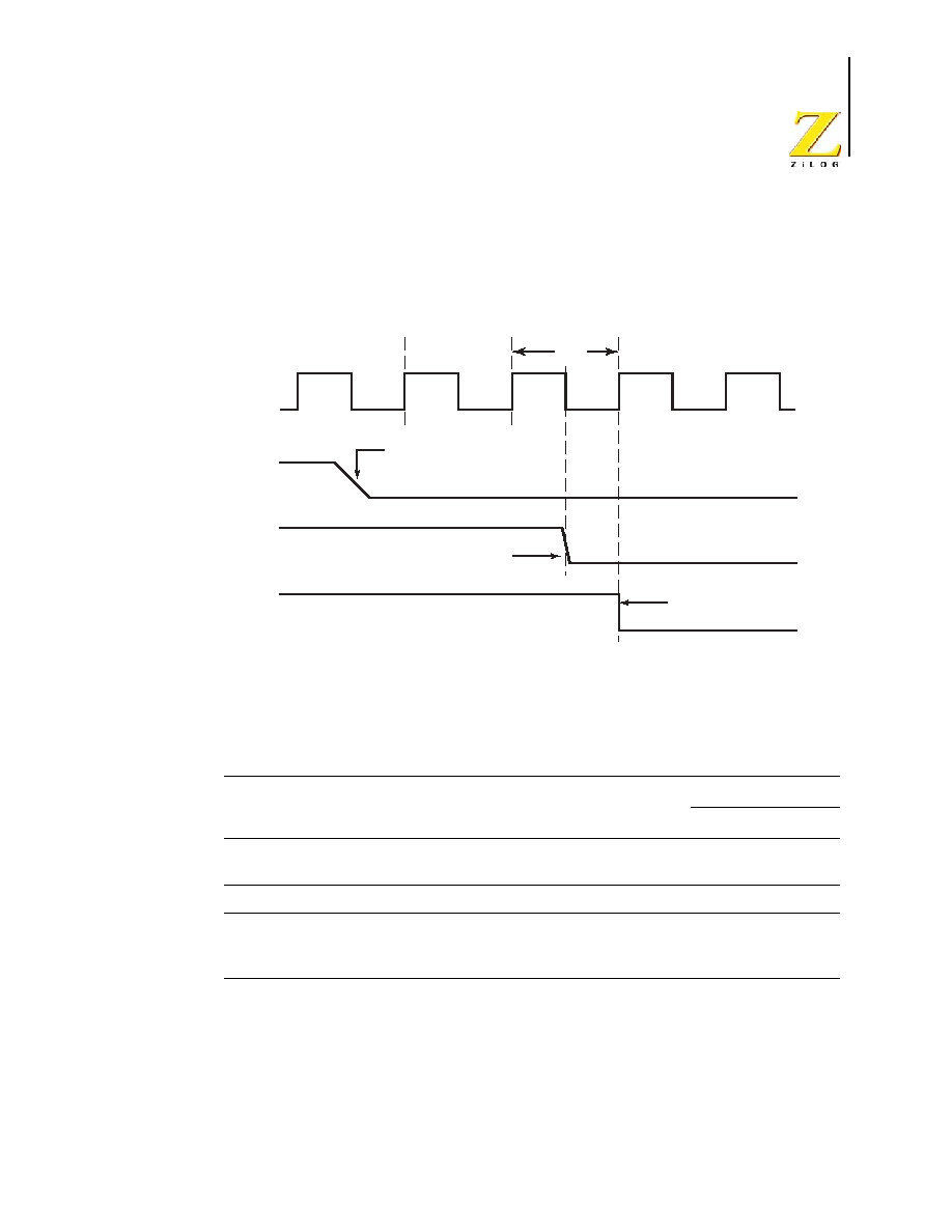
PS024604-1005
P R E L I M I N A R Y
General Purpose I/O Port Input Data Sample
Z8FMC16100 Series Flash MCU
Product Specification
271
General Purpose I/O Port Input Data Sample Timing
Figure 51 illustrates the timing of the GPIO Port input sampling. Table 149 lists the GPIO
port input timing.
Table 149 and Table 150 provide timing information for the GPIO Port inputs and outputs.
Figure 51. Port Input Sample Timing
Table 149. GPIO Port Input Timing
Parameter
Abbreviation
Delay (ns)
Min
Max
T
S_PORT
Port input transition to X
IN
fall setup time
(Not pictured)
5
--
T
H_PORT
X
IN
fall to port input transition hold time (not pictured).
5
--
T
SMR
GPIO port pin pulse width to ensure Stop-Mode
Recovery (for GPIO port pins enabled as SMR
sources) .
1 �s
T
CLK
System
Clock
GPIO Pin
Input Value
GPIO Input
Data Latch
GPIO Data
Read on Data Bus
Port Value
Changes to 0
0 Latched
into Port Input
Data Register
GPIO Data Register
Value 0 Read
by eZ8 CPU

Electrical Characteristics
P R E L I M I N A R Y
PS024604-1005
Z8 Encore!
�
Motor Control Flash MCUs
Product Specification
272
General Purpose I/O Port Output Timing
Figure 52 and Table 150 provide timing information for the GPIO port pins.
Figure 52. GPIO Port Output Timing
Table 150. GPIO Port Output Timing
Parameter
Abbreviation
Delay (ns)
Minimum
Maximum
T
1
X
IN
Rise to Port Output Valid Delay
--
15
T
2
X
IN
Rise to Port Output Hold Time
2
--
T
CLK
X
IN
Port Output
T1
T2

PS024604-1005
P R E L I M I N A R Y On-Chip
Debugger
Timing
Z8FMC16100 Series Flash MCU
Product Specification
273
On-Chip Debugger Timing
Figure 53 and Table 151 provide timing information for the DBG pin. The DBG pin tim-
ing specifications assume a 4 �s maximum rise and fall time.
Figure 53. On-Chip Debugger Timing
Table 151. On-Chip Debugger Timing
Parameter
Abbreviation
Delay (ns)
Minimum
Maximum
T
1
X
IN
Rise to DBG Valid Delay
--
15
T
2
X
IN
Rise to DBG Output Hold Time
2
--
T
3
DBG to X
IN
Rise Input Setup Time
10
--
T
4
DBG to X
IN
Rise Input Hold Time
5
--
DBG Frequency
System
Clock � 4
T
CLK
X
IN
DBG Output
Output Data
T1
T2
DBG Input
Input Data
T4
T3

Electrical Characteristics
P R E L I M I N A R Y
PS024604-1005
Z8 Encore!
�
Motor Control Flash MCUs
Product Specification
274
UART Timing
Figure 54 and Table 152 provide timing information for UART pins for the case where the
Clear To Send input pin (CTS) is used for flow control. In this example, it is assumed that
the Driver Enable polarity has been configured to be Active Low and is represented here
by DE. The CTS to DE assertion delay (T1) assumes the UART Transmit Data Register
has been loaded with data prior to CTS assertion.
Figure 54. UART Timing with CTS
Table 152. UART Timing with CTS
Parameter
Abbreviation
Delay (ns)
Minimum
Maximum
T
1
CTS fall to DE assertion delay
2 x X
IN
period 2 x X
IN
period
+ 1 bit period
T
2
DE assertion to TxD falling edge (start)
delay
1 bit period
1 bit period +
1 x X
IN
period
T
3
End of stop bit(s) to DE deassertion delay 1 x X
IN
period 2 x X
IN
period
T1
T2
T3
End of
Stop Bit(s)
CTS
(Input)
DE
(Output)
TxD
(Output)
Bit 0
Bit 1
Bit 7
Stop
Parity
Start
� � �
� � �
� � �
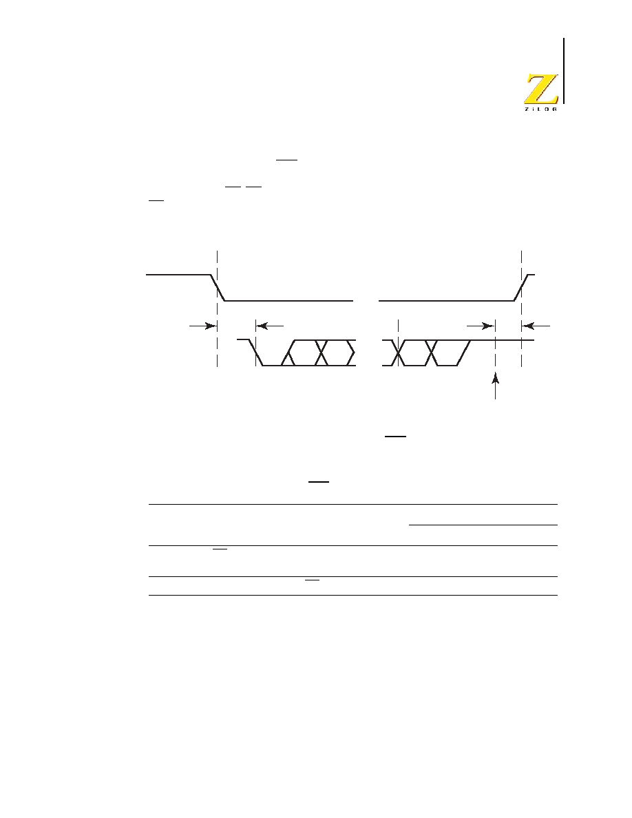
PS024604-1005
P R E L I M I N A R Y UART
Timing
Z8FMC16100 Series Flash MCU
Product Specification
275
Figure 55 and Table 153 provide timing information for UART pins for the case where the
Clear To Send input signal (CTS) is not used for flow control. In this example, it is
assumed that the Driver Enable polarity has been configured to be Active Low and is rep-
resented here by DE. DE asserts after the UART Transmit Data Register has been written.
DE remains asserted for multiple characters as long as the Transmit Data Register is writ-
ten with the next character before the current character has completed.
Figure 55. UART Timing without CTS
Table 153. UART Timing without CTS
Parameter
Abbreviation
Delay (ns)
Minimum
Maximum
T
1
DE assertion to TxD falling edge (start)
delay
1 bit period
1 bit period +
1 x X
IN
period
T
2
End of stop bit(s) to DE deassertion delay 1 x X
IN
period 2 x X
IN
period
T1
T2
End of
Stop Bit(s)
DE
(Output)
TxD
(Output)
Bit 0
Bit 1
Bit 7
Stop
Parity
Start
� � �
� � �

Electrical Characteristics
P R E L I M I N A R Y
PS024604-1005
Z8 Encore!
�
Motor Control Flash MCUs
Product Specification
276

PS024604-1005
P R E L I M I N A R Y
eZ8 CPU Instruction Set
Z8FMC16100 Series Flash MCU
Product Specification
277
eZ8 CPU Instruction Set
This chapter describes how to use the eZ8 CPU.
Assembly Language Programming Introduction
The eZ8 CPU assembly language provides a means for writing an application program
without concern for actual memory addresses or machine instruction formats. A program
written in assembly language is called a source program. Assembly language allows the
use of symbolic addresses to identify memory locations. It also allows mnemonic codes
(Op Codes and operands) to represent the instructions themselves. The Op Codes identify
the instruction while the operands represent memory locations, registers, or immediate
data values.
Each assembly language program consists of a series of symbolic commands called state-
ments. Each statement can contain labels, operations, operands and comments.
Labels can be assigned to a particular instruction step in a source program. The label iden-
tifies that step in the program as an entry point for use by other instructions.
The assembly language also includes assembler directives that supplement the machine
instruction. The assembler directives, or pseudo-ops, are not translated into a machine
instruction. Rather, the pseudo-ops are interpreted as directives that control or assist the
assembly process.
The source program is processed (assembled) by the assembler to obtain a machine lan-
guage program called the object code. The object code is executed by the eZ8 CPU. An
example segment of an assembly language program is detailed in the code below.
Assembly Language Source Program Example
JP START
; Everything after the semicolon is a comment.
START:
; A label called START. The first instruction (JP
START) in this
; example causes program execution to jump to the
point within the
; program where the START label occurs.
LD R4, R7
; A Load (LD) instruction with two operands. The
first operand,
; Working Register R4, is the destination. The
second operand,

PS024604-1005
P R E L I M I N A R Y
eZ8 CPU Instruction Set
Z8 Encore!
�
Motor Control Flash MCUs
Product Specification
278
Assembly Language Syntax
For proper instruction execution, eZ8 CPU assembly language syntax requires that the
operands be written as `destination, source'. After assembly, the object code usually has
the operands in the order 'source, destination', but ordering is Op Code-dependent. The
following instruction examples illustrate the format of some basic assembly instructions
and the resulting object code produced by the assembler. This binary format must be fol-
lowed by users that prefer manual program coding or intend to implement their own
assembler.
Example 1.
If the contents of registers
43h
and
08h
are added and the result is stored in
43h
, the assembly syntax and resulting object code is:
Example 2.
In general, when an instruction format requires an 8-bit register address, that
address can specify any register location in the range 0�255 or, using Escaped Mode
Addressing in working registers R0�R15. If the contents of Register
43h
and Working
Register R8 are added and the result is stored in
43h
, the assembly syntax and resulting
object code is:
; Working Register R7, is the source. The contents
of R7 is
; written into R4.
LD 234H, #%01
; Another Load (LD) instruction with two operands.
; The first operand, Extended Mode Register Address
234H,
; identifies the destination. The second operand,
Immediate Data
; value 01h, is the source. The value 01h is
written into the
; Register at address 234h.
Assembly Language Code
ADD
43H,
08h
(ADD dst, src)
Object Code
04
08
43
(OPC src, dst)
Assembly Language Code
ADD
43H,
R8
(ADD dst, src)
Object Code
04
E8
43
(OPC src, dst)

PS024604-1005
P R E L I M I N A R Y
eZ8 CPU Instruction Set
Z8FMC16100 Series Flash MCU
Product Specification
279
The size of the register file varies depending upon device type. The register file is 512
bytes for the Z8FMC16100 Series Flash MCU.
eZ8 CPU Instruction Notation
In the eZ8 CPU Instruction Summary and Description sections, the operands, condition
codes, status flags, and address modes are represented by a notational shorthand that is
described in Table 154.
.
Table 154. Notational Shorthand
Notation Description
Operand Range
b
Bit
b
b represents a value from 0 to 7 (000b to 111b).
cc
Condition Code
--
See Condition Codes overview in the eZ8 CPU
User Manual (UM0128).
DA
Direct Address
Addrs
Addrs represents a number in the range of 0000h
to FFFFh.
ER
Extended Addressing Register Reg
Reg. represents a number in the range of 000h to
FFFh.
IM
Immediate Data
#Data
Data is a number between 00h to FFh.
Ir
Indirect Working Register
@Rn
n = 0 �15.
IR
Indirect Register
@Reg
Reg. represents a number in the range of 00h to
FFh.
Irr
Indirect Working Register Pair
@RRp
p = 0, 2, 4, 6, 8, 10, 12, or 14.
IRR
Indirect Register Pair
@Reg
Reg. represents an even number in the range 00h
to FEh.
p
Polarity
p
Polarity is a single bit binary value of either 0b or
1b.
r
Working Register
Rn
n = 0�15.
R
Register
Reg
Reg. represents a number in the range of 00h to
FFh.
RA
Relative Address
X
X represents an index in the range of +127 to
�128, which is an offset relative to the address of
the next instruction.
rr
Working Register Pair
RRp
p = 0, 2, 4, 6, 8, 10, 12, or 14.
RR
Register Pair
Reg
Reg. represents an even number in the range of
00h to FEh.
Note:

PS024604-1005
P R E L I M I N A R Y
eZ8 CPU Instruction Set
Z8 Encore!
�
Motor Control Flash MCUs
Product Specification
280
Table 155 contains additional symbols that are used throughout the Instruction Summary
and Instruction Set Description sections.
Assignment of a value is indicated by an arrow. For example,
dst
dst + src
indicates the source data is added to the destination data and the result is stored in the des-
tination location.
Vector
Vector Address
Vector
Vector represents a number in the range of 00h to
FFh.
X
Indexed
#Index
The register or register pair to be indexed is offset
by the signed Index value (#Index) in a +127 to �
128 range.
Table 155. Additional Symbols
Symbol
Definition
dst
Destination Operand
src
Source Operand
@
Indirect Address Prefix
SP
Stack Pointer
PC
Program Counter
FLAGS
Flags Register
RP
Register Pointer
#
Immediate Operand Prefix
B
Binary Number Suffix
%
Hexadecimal Number
Prefix
H
Hexadecimal Number
Suffix
Table 154. Notational Shorthand (Continued)
Notation Description
Operand Range

PS024604-1005
P R E L I M I N A R Y
eZ8 CPU Instruction Set
Z8FMC16100 Series Flash MCU
Product Specification
281
Condition Codes
The C, Z, S, and V flags control the operation of the conditional jump (JP cc and JR cc)
instructions. Sixteen frequently-useful functions of the flag settings are encoded in a 4-bit
field called the condition code (cc), which forms Bits 7:4 of the conditional jump instruc-
tions. Table 156 summarizes the condition codes. Some binary condition codes can be cre-
ated using more than one assembly code mnemonic. The result of the flag test operation
decides whether the conditional jump is executed.
Table 156. Condition Codes
Binary
Hex
Assembly
Mnemonic
Definition
Flag Test Operation
0000
0
F
Always False
--
0001
1
LT
Less Than
(S XOR V) = 1
0010
2
LE
Less Than or Equal
(Z or (S XOR V)) = 1
0011
3
ULE
Unsigned Less Than or Equal (C OR Z) = 1
0100
4
OV
Overflow
V = 1
0101
5
Ml
Minus
S = 1
0110
6
Z
Zero
Z = 1
0110
6
EQ
Equal
Z = 1
0111
7
C
Carry
C = 1
0111
7
ULT
Unsigned Less Than
C = 1
1000
8
T (or blank)
Always True
--
1001
9
GE
Greater Than or Equal
(S XOR V) = 0
1010
A
GT
Greater Than
(Z OR (S XOR V)) = 0
1011
B
UGT
Unsigned Greater Than
(C = 0 AND Z = 0) = 1
1100
C
NOV
No Overflow
V = 0
1101
D
PL
Plus
S = 0
1110
E
NZ
Non-Zero
Z = 0
1110
E
NE
Not Equal
Z = 0
1111
F
NC
No Carry
C = 0
1111
F
UGE
Unsigned Greater Than or
Equal
C = 0

PS024604-1005
P R E L I M I N A R Y
eZ8 CPU Instruction Set
Z8 Encore!
�
Motor Control Flash MCUs
Product Specification
282
eZ8 CPU Instruction Classes
eZ8 CPU
instructions can be divided functionally into the following groups:
�
Arithmetic
�
Bit Manipulation
�
Block Transfer
�
CPU Control
�
Load
�
Logical
�
Program Control
�
Rotate and Shift
Tables 157 through 164 contain the instructions belonging to each group and the number
of operands required for each instruction. Some instructions appear in more than one table
as these instruction can be considered as a subset of more than one category. Within these
tables, the source operand is identified as src, the destination operand is dst and a condi-
tion code is cc.
Table 157. Arithmetic Instructions
Mnemonic
Operands
Instruction
ADC
dst, src
Add with Carry
ADCX
dst, src
Add with Carry using extended addressing
ADD
dst, src
Add
ADDX
dst, src
Add using extended addressing
CP
dst, src
Compare
CPC
dst, src
Compare with Carry
CPCX
dst, src
Compare with Carry using extended addressing
CPX
dst, src
Compare using extended addressing
DA
dst
Decimal Adjust
DEC
dst
Decrement
DECW
dst
Decrement Word
INC
dst
Increment
INCW
dst
Increment Word

PS024604-1005
P R E L I M I N A R Y
eZ8 CPU Instruction Set
Z8FMC16100 Series Flash MCU
Product Specification
283
MULT
dst
Multiply
SBC
dst, src
Subtract with Carry
SBCX
dst, src
Subtract with Carry using extended addressing
SUB
dst, src
Subtract
SUBX
dst, src
Subtract using extended addressing
Table 158. Bit Manipulation Instructions
Mnemonic
Operands
Instruction
BCLR
bit, dst
Bit Clear
BIT
p, bit, dst
Bit Set or Clear
BSET
bit, dst
Bit Set
BSWAP
dst
Bit Swap
CCF
--
Complement Carry Flag
RCF
--
Reset Carry Flag
SCF
--
Set Carry Flag
TCM
dst, src
Test Complement Under Mask
TCMX
dst, src
Test Complement Under Mask using extended
addressing
TM
dst, src
Test Under Mask
TMX
dst, src
Test Under Mask using extended addressing
Table 159. Block Transfer Instructions
Mnemonic
Operands
Instruction
LDCI
dst, src
Load Constant to/from program memory and
autoincrement addresses
LDEI
dst, src
Load External Data to/from data memory and
autoincrement addresses
Table 157. Arithmetic Instructions (Continued)
Mnemonic
Operands
Instruction

PS024604-1005
P R E L I M I N A R Y
eZ8 CPU Instruction Set
Z8 Encore!
�
Motor Control Flash MCUs
Product Specification
284
Table 160. CPU Control Instructions
Mnemonic
Operands
Instruction
CCF
--
Complement Carry Flag
DI
--
Disable Interrupts
EI
--
Enable Interrupts
HALT
--
HALT Mode
NOP
--
No Operation
RCF
--
Reset Carry Flag
SCF
--
Set Carry Flag
SRP
src
Set Register Pointer
STOP
--
STOP mode
WDT
--
Watch-Dog Timer Refresh
Table 161. Load Instructions
Mnemonic
Operands
Instruction
CLR
dst
Clear
LD
dst, src
Load
LDC
dst, src
Load Constant to/from program memory
LDCI
dst, src
Load Constant to/from program memory and
autoincrement addresses
LDE
dst, src
Load External Data to/from data memory
LDEI
dst, src
Load External Data to/from data memory and
autoincrement addresses
LDWX
dst, src
Load Word using extended addressing
LDX
dst, src
Load using extended addressing
LEA
dst, X(src)
Load Effective Address
POP
dst
Pop
POPX
dst
Pop using extended addressing
PUSH
src
Push
PUSHX
src
Push using extended addressing

PS024604-1005
P R E L I M I N A R Y
eZ8 CPU Instruction Set
Z8FMC16100 Series Flash MCU
Product Specification
285
Table 162. Logical Instructions
Mnemonic
Operands
Instruction
AND
dst, src
Logical AND
ANDX
dst, src
Logical AND using extended addressing
COM
dst
Complement
OR
dst, src
Logical OR
ORX
dst, src
Logical OR using extended addressing
XOR
dst, src
Logical Exclusive OR
XORX
dst, src
Logical Exclusive OR using extended addressing
Table 163. Program Control Instructions
Mnemonic
Operands
Instruction
ATM
--
Atomic
BRK
--
On-Chip Debugger Break
BTJ
p, bit, src, DA
Bit Test and Jump
BTJNZ
bit, src, DA
Bit Test and Jump if Non-Zero
BTJZ
bit, src, DA
Bit Test and Jump if Zero
CALL
dst
Call Procedure
DJNZ
dst, src, RA
Decrement and Jump Non-Zero
IRET
--
Interrupt Return
JP
dst
Jump
JP cc
dst
Jump Conditional
JR
DA
Jump Relative
JR cc
DA
Jump Relative Conditional
RET
--
Return
TRAP
vector
Software Trap
Table 164. Rotate and Shift Instructions
Mnemonic
Operands
Instruction
BSWAP
dst
Bit Swap
RL
dst
Rotate Left

PS024604-1005
P R E L I M I N A R Y
eZ8 CPU Instruction Set
Z8 Encore!
�
Motor Control Flash MCUs
Product Specification
286
eZ8 CPU Instruction Summary
Table 165 summarizes the eZ8 CPU instructions. The table identifies the addressing
modes employed by the instruction, the effect upon the Flags Register, the number of CPU
clock cycles required for the instruction fetch, and the number of CPU clock cycles
required for the instruction execution.
.
RLC
dst
Rotate Left through Carry
RR
dst
Rotate Right
RRC
dst
Rotate Right through Carry
SRA
dst
Shift Right Arithmetic
SRL
dst
Shift Right Logical
SWAP
dst
Swap Nibbles
Table 165. eZ8 CPU Instruction Summary
Assembly
Mnemonic
Symbolic Operation
Address
Mode
Op
Code(s)
(Hex)
Flags
Fetch
Cycles
Instr.
Cycles
dst src
C Z S V D H
ADC dst, src
dst
dst + src + C
r
r
12
*
*
*
*
0
*
2
3
r
Ir
13
2
4
R
R
14
3
3
R
IR
15
3
4
R
IM
16
3
3
IR
IM
17
3
4
ADCX dst, src
dst
dst + src + C
ER ER
18
*
*
*
*
0
*
4
3
ER
IM
19
4
3
Note: Flags Notation:
* = Value is a function of the result of the operation.
� = unaffected.
X = undefined.
0 = reset to 0.
1 = set to 1.
Table 164. Rotate and Shift Instructions (Continued)
Mnemonic
Operands
Instruction

PS024604-1005
P R E L I M I N A R Y
eZ8 CPU Instruction Set
Z8FMC16100 Series Flash MCU
Product Specification
287
ADD dst, src
dst
dst + src
r
r
02
*
*
*
*
0
*
2
3
r
Ir
03
2
4
R
R
04
3
3
R
IR
05
3
4
R
IM
06
3
3
IR
IM
07
3
4
ADDX dst, src
dst
dst + src
ER ER
08
*
*
*
*
0
*
4
3
ER
IM
09
4
3
AND dst, src
dst
dst + src
r
r
52
-- *
*
0 -- --
2
3
r
Ir
53
2
4
R
R
54
3
3
R
IR
55
3
4
R
IM
56
3
3
IR
IM
57
3
4
ANDX dst, src
dst
dst AND src
ER ER
58
-- *
*
0 -- --
4
3
ER
IM
59
4
3
ATM
Atomic execution
2F
-- -- -- -- -- --
1
1
BCLR bit, dst
dst[bit]
0
r
E2
-- *
*
0 -- --
2
2
BIT p, bit, dst
dst[bit]
p
r
E2
-- *
*
0 -- --
2
2
BRK
Debugger Break
00
-- -- -- -- -- --
1
1
BSET bit, dst
dst[bit]
1
r
E2
-- *
*
0 -- --
2
2
BSWAP dst
dst[7:0]
dst[0:7]
R
D5
X
*
*
0
-
-
2
2
BTJ p, bit, src,
dst
if src[bit] = p
PC
PC + X
r
F6
-- -- -- -- -- --
3
3
Ir
F7
3
4
Table 165. eZ8 CPU Instruction Summary (Continued)
Assembly
Mnemonic
Symbolic Operation
Address
Mode
Op
Code(s)
(Hex)
Flags
Fetch
Cycles
Instr.
Cycles
dst src
C Z S V D H
Note: Flags Notation:
* = Value is a function of the result of the operation.
� = unaffected.
X = undefined.
0 = reset to 0.
1 = set to 1.

PS024604-1005
P R E L I M I N A R Y
eZ8 CPU Instruction Set
Z8 Encore!
�
Motor Control Flash MCUs
Product Specification
288
BTJNZ bit, src,
dst
if src[bit] = 1
PC
PC + X
r
F6
-- -- -- -- -- --
3
3
Ir
F7
3
4
BTJZ bit, src,
dst
if src[bit] = 0
PC
PC + X
r
F6
-- -- -- -- -- --
3
3
Ir
F7
3
4
CALL dst
SP
SP � 2
@SP
PC
PC
dst
IRR
D4
-- -- -- -- -- --
2
6
DA
D6
3
3
CCF
C
~C
EF
* -- -- -- -- --
1
2
CLR dst
dst
00h
R
B0
-- -- -- -- -- --
2
2
IR
B1
2
3
COM dst
dst
~dst
R
60
-- *
*
0 -- --
2
2
IR
61
2
3
CP dst, src
dst � src
r
r
A2
*
*
*
* -- --
2
3
r
Ir
A3
2
4
R
R
A4
3
3
R
IR
A5
3
4
R
IM
A6
3
3
IR
IM
A7
3
4
CPC dst, src
dst � src � C
r
r
1F A2
*
*
*
* -- --
3
3
r
Ir
1F A3
3
4
R
R
1F A4
4
3
R
IR
1F A5
4
4
R
IM
1F A6
4
3
IR
IM
1F A7
4
4
Table 165. eZ8 CPU Instruction Summary (Continued)
Assembly
Mnemonic
Symbolic Operation
Address
Mode
Op
Code(s)
(Hex)
Flags
Fetch
Cycles
Instr.
Cycles
dst src
C Z S V D H
Note: Flags Notation:
* = Value is a function of the result of the operation.
� = unaffected.
X = undefined.
0 = reset to 0.
1 = set to 1.

PS024604-1005
P R E L I M I N A R Y
eZ8 CPU Instruction Set
Z8FMC16100 Series Flash MCU
Product Specification
289
CPCX dst, src
dst � src � C
ER ER
1F A8
*
*
*
* -- --
5
3
ER
IM
1F A9
5
3
CPX dst, src
dst � src
ER ER
A8
*
*
*
* -- --
4
3
ER
IM
A9
4
3
DA dst
dst
DA(dst)
R
40
*
*
*
X -- --
2
2
IR
41
2
3
DEC dst
dst
dst � 1
R
30
-- *
*
*
v --
2
2
IR
31
2
3
DECW dst
dst
dst � 1
RR
80
-- *
*
* -- --
2
5
IRR
81
2
6
DI
IRQE
0
8F
-- -- -- -- -- --
1
2
DJNZ dst, RA
dst
dst � 1
if dst
0
PC
PC + X
r
0A�FA
-- -- -- -- -- --
2
3
EI
IRQE
1
9F
-- -- -- -- -- --
1
2
HALT
HALT Mode
7F
-- -- -- -- -- --
1
2
INC dst
dst
dst + 1
R
20
-- *
*
* -- --
2
2
IR
21
2
3
r
0E�FE
1
2
INCW dst
dst
dst + 1
RR
A0
-- *
*
* -- --
2
5
IRR
A1
2
6
IRET
FLAGS
@SP
SP
SP + 1
PC
@SP
SP
SP + 2
IRQE
1
BF
*
*
*
*
*
*
1
5
Table 165. eZ8 CPU Instruction Summary (Continued)
Assembly
Mnemonic
Symbolic Operation
Address
Mode
Op
Code(s)
(Hex)
Flags
Fetch
Cycles
Instr.
Cycles
dst src
C Z S V D H
Note: Flags Notation:
* = Value is a function of the result of the operation.
� = unaffected.
X = undefined.
0 = reset to 0.
1 = set to 1.

PS024604-1005
P R E L I M I N A R Y
eZ8 CPU Instruction Set
Z8 Encore!
�
Motor Control Flash MCUs
Product Specification
290
JP dst
PC
dst
DA
8D
-- -- -- -- -- --
3
2
IRR
C4
2
3
JP cc, dst
if cc is true
PC
dst
DA
0D�FD
-- -- -- -- -- --
3
2
JR dst
PC
PC + X
DA
8B
-- -- -- -- -- --
2
2
JR cc, dst
if cc is true
PC
PC + X
DA
0B�FB
-- -- -- -- -- --
2
2
LD dst, rc
dst
src
r
IM
0C�FC
-- -- -- -- -- --
2
2
r
X(r)
C7
3
3
X(r)
r
D7
3
4
r
Ir
E3
2
3
R
R
E4
3
2
R
IR
E5
3
4
R
IM
E6
3
2
IR
IM
E7
3
3
Ir
r
F3
2
3
IR
R
F5
3
3
LDC dst, src
dst
src
r
Irr
C2
-- -- -- -- -- --
2
5
Ir
Irr
C5
2
9
Irr
r
D2
2
5
LDCI dst, src
dst
src
r
r + 1
rr
rr + 1
Ir
Irr
C3
-- -- -- -- -- --
2
9
Irr
Ir
D3
2
9
LDE dst, src
dst
src
r
Irr
82
-- -- -- -- -- --
2
5
Irr
r
92
2
5
Table 165. eZ8 CPU Instruction Summary (Continued)
Assembly
Mnemonic
Symbolic Operation
Address
Mode
Op
Code(s)
(Hex)
Flags
Fetch
Cycles
Instr.
Cycles
dst src
C Z S V D H
Note: Flags Notation:
* = Value is a function of the result of the operation.
� = unaffected.
X = undefined.
0 = reset to 0.
1 = set to 1.

PS024604-1005
P R E L I M I N A R Y
eZ8 CPU Instruction Set
Z8FMC16100 Series Flash MCU
Product Specification
291
LDEI dst, src
dst
src
r
r + 1
rr
rr + 1
Ir
Irr
83
-- -- -- -- -- --
2
9
Irr
Ir
93
2
9
LDWX dst, src
dst
src
ER ER
1F E8
-- -- -- -- -- --
5
4
LDX dst, src
dst
src
r
ER
84
-- -- -- -- -- --
3
2
Ir
ER
85
3
3
R
IRR
86
3
4
IR IRR
87
3
5
r
X(rr)
88
3
4
X(rr)
r
89
3
4
ER
r
94
3
2
ER
Ir
95
3
3
IRR
R
96
3
4
IRR IR
97
3
5
ER ER
E8
4
2
ER
IM
E9
4
2
LEA dst, X(src) dst
src + X
r
X(r)
98
-- -- -- -- -- --
3
3
rr X(rr)
99
3
5
MULT dst
dst[15:0]
dst[15:8] * dst[7:0]
RR
F4
-- -- -- -- -- --
2
8
NOP
No operation
0F
-- -- -- -- -- --
1
2
Table 165. eZ8 CPU Instruction Summary (Continued)
Assembly
Mnemonic
Symbolic Operation
Address
Mode
Op
Code(s)
(Hex)
Flags
Fetch
Cycles
Instr.
Cycles
dst src
C Z S V D H
Note: Flags Notation:
* = Value is a function of the result of the operation.
� = unaffected.
X = undefined.
0 = reset to 0.
1 = set to 1.
PS024604-1005
P R E L I M I N A R Y
eZ8 CPU Instruction Set
Z8 Encore!
�
Motor Control Flash MCUs
Product Specification
292
OR dst, src
dst
dst OR src
r
r
42
-- *
*
0 -- --
2
3
r
Ir
43
2
4
R
R
44
3
3
R
IR
45
3
4
R
IM
46
3
3
IR
IM
47
3
4
ORX dst, src
dst
dst OR src
ER ER
48
-- *
*
0 -- --
4
3
ER
IM
49
4
3
POP dst
dst
@SP
SP
SP + 1
R
50
-- -- -- -- -- --
2
2
IR
51
2
3
POPX dst
dst
@SP
SP
SP + 1
ER
D8
-- -- -- -- -- --
3
2
PUSH src
SP
SP � 1
@SP
src
R
70
-- -- -- -- -- --
2
2
IR
71
2
3
IM
1F 70
3
2
PUSHX src
SP
SP � 1
@SP
src
ER
C8
-- -- -- -- -- --
3
2
RCF
C
0
CF
0 -- -- -- -- --
1
2
RET
PC
@SP
SP
SP + 2
AF
-- -- -- -- -- --
1
4
RL dst
R
90
*
*
*
* -- --
2
2
IR
91
2
3
RLC dst
R
10
*
*
*
* -- --
2
2
IR
11
2
3
Table 165. eZ8 CPU Instruction Summary (Continued)
Assembly
Mnemonic
Symbolic Operation
Address
Mode
Op
Code(s)
(Hex)
Flags
Fetch
Cycles
Instr.
Cycles
dst src
C Z S V D H
Note: Flags Notation:
* = Value is a function of the result of the operation.
� = unaffected.
X = undefined.
0 = reset to 0.
1 = set to 1.
D7 D6 D5 D4 D3 D2 D1 D0
dst
C
D7 D6 D5 D4 D3 D2 D1 D0
dst
C
PS024604-1005
P R E L I M I N A R Y
eZ8 CPU Instruction Set
Z8FMC16100 Series Flash MCU
Product Specification
293
RR dst
R
E0
*
*
*
* -- --
2
2
IR
E1
2
3
RRC dst
R
C0
*
*
*
* -- --
2
2
IR
C1
2
3
SBC dst, src
dst
dst � src � C
r
r
32
*
*
*
*
1
*
2
3
r
Ir
33
2
4
R
R
34
3
3
R
IR
35
3
4
R
IM
36
3
3
IR
IM
37
3
4
SBCX dst, src
dst
dst � src � C
ER ER
38
*
*
*
*
1
*
4
3
ER
IM
39
4
3
SCF
C
1
DF
1 -- -- -- -- --
1
2
SRA dst
R
D0
*
*
*
0 -- --
2
2
IR
D1
2
3
SRL dst
R
1F C0
*
*
0
* -- --
3
2
IR
1F C1
3
3
SRP src
RP
src
IM
01
-- -- -- -- -- --
2
2
STOP
STOP mode
6F
-- -- -- -- -- --
1
2
Table 165. eZ8 CPU Instruction Summary (Continued)
Assembly
Mnemonic
Symbolic Operation
Address
Mode
Op
Code(s)
(Hex)
Flags
Fetch
Cycles
Instr.
Cycles
dst src
C Z S V D H
Note: Flags Notation:
* = Value is a function of the result of the operation.
� = unaffected.
X = undefined.
0 = reset to 0.
1 = set to 1.
D7 D6 D5 D4 D3 D2 D1 D0
dst
C
D7 D6 D5 D4 D3 D2 D1 D0
dst
C
D7 D6 D5 D4 D3 D2 D1 D0
dst
C
D7 D6 D5 D4 D3 D2 D1 D0
dst
C
0

PS024604-1005
P R E L I M I N A R Y
eZ8 CPU Instruction Set
Z8 Encore!
�
Motor Control Flash MCUs
Product Specification
294
SUB dst, src
dst
dst � src
r
r
22
*
*
*
*
1
*
2
3
r
Ir
23
2
4
R
R
24
3
3
R
IR
25
3
4
R
IM
26
3
3
IR
IM
27
3
4
SUBX dst, src
dst
dst � src
ER ER
28
*
*
*
*
1
*
4
3
ER
IM
29
4
3
SWAP dst
dst[7:4]
dst[3:0]
R
F0
X
*
*
X -- --
2
2
IR
F1
2
3
TCM dst, src
(NOT dst) AND src
r
r
62
-- *
*
0 -- --
2
3
r
Ir
63
2
4
R
R
64
3
3
R
IR
65
3
4
R
IM
66
3
3
IR
IM
67
3
4
TCMX dst, src
(NOT dst) AND src
ER ER
68
-- *
*
0 -- --
4
3
ER
IM
69
4
3
TM dst, src
dst AND src
r
r
72
-- *
*
0 -- --
2
3
r
Ir
73
2
4
R
R
74
3
3
R
IR
75
3
4
R
IM
76
3
3
IR
IM
77
3
4
Table 165. eZ8 CPU Instruction Summary (Continued)
Assembly
Mnemonic
Symbolic Operation
Address
Mode
Op
Code(s)
(Hex)
Flags
Fetch
Cycles
Instr.
Cycles
dst src
C Z S V D H
Note: Flags Notation:
* = Value is a function of the result of the operation.
� = unaffected.
X = undefined.
0 = reset to 0.
1 = set to 1.

PS024604-1005
P R E L I M I N A R Y
eZ8 CPU Instruction Set
Z8FMC16100 Series Flash MCU
Product Specification
295
Flags Register
The Flags Register contains the status information regarding the most recent arithmetic,
logical, bit manipulation or rotate and shift operation. The Flags Register contains six bits
of status information that are set or cleared by CPU operations. Four of the bits (C, V, Z,
and S) can be tested for use with conditional jump instructions. Two flags (H and D) can-
not be tested and are used for Binary-Coded Decimal (BCD) arithmetic.
The two remaining bits, User Flags (F1 and F2), are available as general-purpose status
bits. User Flags are unaffected by arithmetic operations and must be set or cleared by
instructions. The User Flags cannot be used with conditional Jumps. They are undefined at
TMX dst, src
dst AND src
ER ER
78
-- *
*
0 -- --
4
3
ER
IM
79
4
3
TRAP Vector
SP
SP � 2
@SP
PC
SP
SP � 1
@SP
FLAGS
PC
@Vector
Vect
or
F2
-- -- -- -- -- --
2
6
WDT
5F
-- -- -- -- -- --
1
2
XOR dst, src
dst
dst XOR src
r
r
B2
-- *
*
0 -- --
2
3
r
Ir
B3
2
4
R
R
B4
3
3
R
IR
B5
3
4
R
IM
B6
3
3
IR
IM
B7
3
4
XORX dst, src
dst
dst XOR src
ER ER
B8
-- *
*
0 -- --
4
3
ER
IM
B9
4
3
Table 165. eZ8 CPU Instruction Summary (Continued)
Assembly
Mnemonic
Symbolic Operation
Address
Mode
Op
Code(s)
(Hex)
Flags
Fetch
Cycles
Instr.
Cycles
dst src
C Z S V D H
Note: Flags Notation:
* = Value is a function of the result of the operation.
� = unaffected.
X = undefined.
0 = reset to 0.
1 = set to 1.
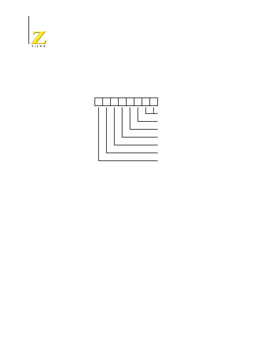
PS024604-1005
P R E L I M I N A R Y
eZ8 CPU Instruction Set
Z8 Encore!
�
Motor Control Flash MCUs
Product Specification
296
initial power-up and are unaffected by Reset. Figure 56 illustrates the flags and their bit
positions in the Flags Register.
Interrupts, the software trap (TRAP) instruction, and illegal instruction traps all write the
value of the Flags Register to the stack. Executing an Interrupt Return (IRET) instruction
restores the value saved on the stack into the Flags Register.
U = Undefined
Figure 56. Flags Register
C
Z
S
V D H F2 F1
Flags Register
Bit
0
Bit
7
Half Carry Flag
Decimal Adjust Flag
Overflow Flag
Sign Flag
Zero Flag
Carry Flag
User Flags
PS024604-1005
P R E L I M I N A R Y Op
Code
Maps
Z8FMC16100 Series Flash MCU
Product Specification
297
Op Code Maps
Figure 57 and Table 166 provide descriptions of the Op Code map data and the abbrevia-
tions. Figures 58 and 59 provide information about each of the eZ8 CPU instructions.
Figure 57. Op Code Map Cell Description
Table 166. Op Code Map Abbreviations
Abbreviation
Description
Abbreviation
Description
b
Bit position
IRR
Indirect Register Pair
cc
Condition code
p
Polarity (0 or 1)
X
8-bit signed index or
displacement
r
4-bit Working Register
DA
Destination address
R
8-bit register
ER
Extended Addressing register
r1, R1, Ir1, Irr1, IR1,
rr1, RR1, IRR1, ER1
Destination address
IM
Immediate data value
r2, R2, Ir2, Irr2, IR2,
rr2, RR2, IRR2, ER2
Source address
Ir
Indirect Working Register
RA
Relative
IR
Indirect register
rr
Working Register Pair
Irr
Indirect Working Register Pair RR
Register Pair
Fetch Cycles
Instruction Cycles
First Operand
After Assembly
Op Code
Upper Nibble
Op Code
Lower Nibble
4
3.3
CP
A
R2,R1
Second Operand
After Assembly
PS024604-1005
P R E L I M I N A R Y Op
Code
Maps
Z8 Encore!
�
Motor Control Flash MCUs
Product Specification
298
Figure 58. First Op Code Map
CP
3.3
R2,R1
CP
3.4
IR2,R1
CP
2.3
r1,r2
CP
2.4
r1,Ir2
CPX
4.3
ER2,ER1
CPX
4.3
IM,ER1
CP
3.3
R1,IM
CP
3.4
IR1,IM
RRC
2.2
R1
RRC
2.3
IR1
0
1
2
3
4
5
6
7
8
9
A
B
C
D
E
F
0
1
2
3
4
5
6
7
8
9
A
B
C
D
E
F
Lower Nibble (Hex)
Up
per
Ni
bbl
e (
H
ex
)
BRK
1.1
SRP
2.2
IM
ADD
2.3
r1,r2
ADD
2.4
r1,Ir2
ADD
3.3
R2,R1
ADD
3.4
IR2,R1
ADD
3.3
R1,IM
ADD
3.4
IR1,IM
ADDX
4.3
ER2,ER1
ADDX
4.3
IM,ER1
DJNZ
2.3
r1,X
JR
2.2
cc,X
LD
2.2
r1,IM
JP
3.2
cc,DA
INC
1.2
r1
NOP
1.2
RLC
2.2
R1
RLC
2.3
IR1
ADC
2.3
r1,r2
ADC
2.4
r1,Ir2
ADC
3.3
R2,R1
ADC
3.4
IR2,R1
ADC
3.3
R1,IM
ADC
3.4
IR1,IM
ADCX
4.3
ER2,ER1
ADCX
4.3
IM,ER1
INC
2.2
R1
INC
2.3
IR1
SUB
2.3
r1,r2
SUB
2.4
r1,Ir2
SUB
3.3
R2,R1
SUB
3.4
IR2,R1
SUB
3.3
R1,IM
SUB
3.4
IR1,IM
SUBX
4.3
ER2,ER1
SUBX
4.3
IM,ER1
DEC
2.2
R1
DEC
2.3
IR1
SBC
2.3
r1,r2
SBC
2.4
r1,Ir2
SBC
3.3
R2,R1
SBC
3.4
IR2,R1
SBC
3.3
R1,IM
SBC
3.4
IR1,IM
SBCX
4.3
ER2,ER1
SBCX
4.3
IM,ER1
DA
2.2
R1
DA
2.3
IR1
OR
2.3
r1,r2
OR
2.4
r1,Ir2
OR
3.3
R2,R1
OR
3.4
IR2,R1
OR
3.3
R1,IM
OR
3.4
IR1,IM
ORX
4.3
ER2,ER1
ORX
4.3
IM,ER1
POP
2.2
R1
POP
2.3
IR1
AND
2.3
r1,r2
AND
2.4
r1,Ir2
AND
3.3
R2,R1
AND
3.4
IR2,R1
AND
3.3
R1,IM
AND
3.4
IR1,IM
ANDX
4.3
ER2,ER1
ANDX
4.3
IM,ER1
COM
2.2
R1
COM
2.3
IR1
TCM
2.3
r1,r2
TCM
2.4
r1,Ir2
TCM
3.3
R2,R1
TCM
3.4
IR2,R1
TCM
3.3
R1,IM
TCM
3.4
IR1,IM
TCMX
4.3
ER2,ER1
TCMX
4.3
IM,ER1
PUSH
2.2
R2
PUSH
2.3
IR2
TM
2.3
r1,r2
TM
2.4
r1,Ir2
TM
3.3
R2,R1
TM
3.4
IR2,R1
TM
3.3
R1,IM
TM
3.4
IR1,IM
TMX
4.3
ER2,ER1
TMX
4.3
IM,ER1
DECW
2.5
RR1
DECW
2.6
IRR1
LDE
2.5
r1,Irr2
LDEI
2.8
Ir1,Irr2
LDX
3.2
r1,ER2
LDX
3.3
Ir1,ER2
LDX
3.4
IRR2,R1
LDX
3.5
IRR2,IR1
LDX
3
3.4
r1,rr2,X
LDX
3
3.4
rr1,r2,X
RL
2.2
R1
RL
2.3
IR1
LDE
2.5
r2,Irr1
LDEI
2.8
Ir2,Irr1
LDX
3.2
r2,ER1
LDX
3.3
Ir2,ER1
LDX
3.4
R2,IRR1
LDX
3.5
IR2,IRR1
LEA
3.3
r1,r2,X
LEA
3
3.5
rr1,rr2,X
INCW
2.5
RR1
INCW
2.6
IRR1
CLR
2.2
R1
CLR
2.3
IR1
XOR
2.3
r1,r2
XOR
2.4
r1,Ir2
XOR
3.3
R2,R1
XOR
3.4
IR2,R1
XOR
3.3
R1,IM
XOR
3.4
IR1,IM
XORX
4.3
ER2,ER1
XORX
4.3
IM,ER1
LDC
2.5
r1,Irr2
LDCI
2.8
Ir1,Irr2
LDC
2.5
r2,Irr1
LDCI
2.8
Ir2,Irr1
JP
2
2.3
IRR1
LDC
2.8
Ir1,Irr2
LD
3.4
r1,r2,X
PUSHX
3
3.3
ER2
SRA
2.2
R1
SRA
2.3
IR1
POPX
3
3.3
ER1
LD
3.4
r2,r1,X
CALL
2
2.6
IRR1
BSWAP
2.2
R1
CALL
3.3
DA
LD
3.2
R2,R1
LD
3.3
IR2,R1
BIT
2.2
p,b,r1
LD
2.3
r1,Ir2
LDX
4.2
ER2,ER1
LDX
4.2
IM,ER1
LD
3.3
R1,IM
LD
3.4
IR1,IM
RR
2.2
R1
RR
2.3
IR1
MULT
2.9
RR1
LD
3.3
R2,IR1
TRAP
2.6
Vector
LD
2.3
Ir1,r2
BTJ
3.3
p,b,r1,X
BTJ
3.4
p,b,Ir1,X
SWAP
2.2
R1
SWAP
2.3
IR1
RCF
1.2
WDT
1.2
STOP
1.2
HALT
1.2
DI
1.2
EI
1.2
RET
1.4
IRET
1.5
SCF
1.2
CCF
1.2
Op Code
See 2nd
Map
ATM
1.1

PS024604-1005
P R E L I M I N A R Y Op
Code
Maps
Z8FMC16100 Series Flash MCU
Product Specification
299
Figure 59. Second Op Code Map After 1Fh
CPC
4.3
R2,R1
CPC
4.4
IR2,R1
CPC
3.3
r1,r2
CPC
3.4
r1,Ir2
CPCX
5.3
ER2,ER1
CPCX
5.3
IM,ER1
CPC
4.3
R1,IM
CPC
4.4
IR1,IM
SRL
3.2
R1
SRL
3.3
IR1
0
1
2
3
4
5
6
7
8
9
A
B
C
D
E
F
0
1
2
3
4
5
6
7
8
9
A
B
C
D
E
F
Lower Nibble (Hex)
Up
per
Nib
b
l
e
(
H
ex
)
PUSH
3.2
IM
LDWX
4.2
ER2,ER1

PS024604-1005
P R E L I M I N A R Y Op
Code
Maps
Z8 Encore!
�
Motor Control Flash MCUs
Product Specification
300

PS024604-1005
P R E L I M I N A R Y Packaging
Z8FMC16100 Series Flash MCU
Product Specification
301
Packaging
Figure 60 illustrates the 32-pin quad flat no lead (QFN) package available for the
Z8FMC16100 Series Flash MCU.
Figure 60. 32-Pin Quad Flat No Lead Package
Figure 61 illustrates the 32-pin low quad flat package (LQFP) available for the
Z8FMC16100 Series Flash MCU.
Figure 61. 32-Pin Low Quad Flat Package

PS024604-1005
P R E L I M I N A R Y Ordering
Information
Z8 Encore!
�
Motor Control Flash MCUs
Product Specification
302
Ordering Information
Table 167 identifies the basic features available for each device within the Z8FMC16100
Series Flash MCU product line. Table 168 provides ordering information for these prod-
ucts by part number. See the
Part Number Description
section on page 304 for a descrip-
tion of a part number's unique identifying attributes.
Each of the parts listed in Table 168 is shown in a lead-free package. The use of lead-free
packaging adheres to a socially responsible environmental standard. To order the standard
plastic (lead-soldered) package, please contact
ZiLOG Customer Service
.
Table 167. Z8FMC16100 Series Part Selection Guide
Product Feature
Z8FMC16100 Z8FMC08100 Z8FMC04100
Flash (KB)
16
8
4
SRAM (B)
512
512
512
General-Purpose I/O
17
17
17
Motor Control PWM Channels
6
6
6
ADC Inputs
8
8
8
Operational Amplifier
Yes
Yes
Yes
Comparator
Yes
Yes
Yes
16-bit Standard Timers w/ Capture, Compare, PWM
Yes
Yes
Yes
UART with support for LIN, and IrDA
Yes
Yes
Yes
I
2
C or SPI Controller
Yes
Yes
Yes
Watch-Dog Timer
Yes
Yes
Yes
5.5296 MHz Internal Precision Oscillator
Yes
Yes
Yes
Z8FMC16100
Yes
Yes
Yes

PS024604-1005
P R E L I M I N A R Y Ordering
Information
Z8FMC16100 Series Flash MCU
Product Specification
303
Navigate your browser to ZiLOG's website to order the Z8FMC16100 Series Flash MCU.
Or, contact your local
ZiLOG Sales Office
. ZiLOG provides additional assistance on its
Customer Service
page, and is also here to help with
Technical Support
issues. For
ZILOG's valuable
development tools and downloadable software
, visit the
ZiLOG web-
site
.
Table 168. Ordering Information for the Z8FMC16100 Series Products*
Part Number
Flash KB
(Bytes)
SRAM
Bytes GPIO
Max.
Speed
(MHz)
I
2
C/SPI
Trimmed
IPO
Package
Temp (�C)
Z8FMC16100 with 16 KB Flash and 512 B SRAM
Z8FMC16100QKSG
16
(16,384)
512
17
20
I
2
C/SPI
Y
QFN-32
0
to +70
Z8FMC16100QKEG
�40
to +105
Z8FMC16100AKSG
16
(16,384)
512
17
20
I
2
C/SPI
Y
LQFP-32
0
to +70
Z8FMC16100AKEG
�40
to +105
Z8FMC08100 with 8 KB Flash and 512 B SRAM
Z8FMC08100QKSG
8 (8,192)
512
17
20
I
2
C/SPI
Y
QFN-32
0
to +70
Z8FMC08100QKEG
�40
to +105
Z8FMC08100AKSG
8 (8,192)
512
17
20
I
2
C/SPI
Y
LQFP-32
0
to +70
Z8FMC08100AKEG
�40
to +105
Z8FMC04100 with 4 KB Flash and 512 B SRAM
Z8FMC04100QKSG
4 (4,096)
512
17
20
I
2
C/SPI
Y
QFN-32
0
to +70
Z8FMC04100QKEG
�40
to +105
Z8FMC04100AKSG
4 (4,096)
512
17
20
I
2
C/SPI
Y
LQFP-32
0
to +70
Z8FMC04100AKEG
�40
to +105
Z8FMC16100 Series Development Kit
Z8FMC160100KIT
Z8FMC16100
Series Development Kit
Z8FMC161000ZEM
Z8 Encore! Z8FMC16100 Series In-Circuit Emulator Development Tool
ZUSBOPTSC01ZAC USB Opto-isolated Smart Cable Accessory Kit
*Note: Factory-programmed versions of the devices in this table are available upon request from ZiLOG.

PS024604-1005
P R E L I M I N A R Y Ordering
Information
Z8 Encore!
�
Motor Control Flash MCUs
Product Specification
304
Part Number Description
ZiLOG part numbers consist of a number of components, as indicated in the following
examples:
Example
Part number Z8FMC16100QKSG is a 16-bit Flash Motor Controller with 16 KB Program
Memory in a QFN package with 32 pins, operating over a 0�C to +70�C temperature range
and built using lead-free solder.
Precharacterization Product
The product represented by this document is newly introduced and ZiLOG has not com-
pleted the full characterization of the product. The document states what ZiLOG knows
about this product at this time, but additional features or nonconformance with some
aspects of the document might be found, either by ZiLOG or its customers in the course of
further application and characterization work. In addition, ZiLOG cautions that delivery
might be uncertain at times due to start-up yield issues.
Z8
ZiLOG 8-bit microcontroller product
FMC
Flash Motor Controller
16
Memory size
100
Product family
Q
Package type
K
Pin count
S
Temperature
G
Environmental flow*
Note: *An environmental flow of G represents the lead-
free packaging option.
Packages
A = LQFP
Q = QFN
Pin Count
K = 32 pins
Temperature
E = �40�C to +105�C
S = 0�C to +70�C
Environmental Flow
C = Plastic Standard
G = Lead-Free

PS024604-1005
P R E L I M I N A R Y Document
Information
Z8FMC16100 Series Flash MCU
Product Specification
305
Document Information
Document Number Description
The Document Control Number that appears in the footer on each page of this document
contains unique identifying attributes, as indicated in the following table:
PS
Product Specification
0246
Unique Document Number
02
Revision Number
0605
Month and Year Published

PS024604-1005
P R E L I M I N A R Y Document
Information
Z8 Encore!
�
Motor Control Flash MCUs
Product Specification
306
Change Log
Rev
Date
Sections
01
April
2005
Original issue
02
August
2005
Revised GPIO count and packages. Updated Figure 60 on page 301.
Added 8K (FMC08100) and 4K (FMC04100) parts to the
Z8FMC16100 Series Flash MCU
Features
section on page 1,
Block Diagram
section on page 2,
Program Memory
section on
page 14,
Program Memory
chapter on page 211, and
Ordering Information
section on page
302 for CR 6264.
Added USB Opto-isolated Smart Cable Accessory Kit to
Ordering Information
section on page
302.
Removed Sample and Hold from
Block Diagram
section on page 2 and
Ordering Information
section on page 302. Updated Figure 36 on page 200. Replaced "Current-Sense Sample and
Hold Control Register" section with
Current Sense ADC Trigger Control Register
section on
page 87.
Removed "Operational Amplifier" chapter for CR 6261.
Updated
Z8FMC16100 Series Flash MCU Features
section on page 1 for CR 6262.
Updated
General-Purpose I/O
chapter on page 35.
Updated
Watch-Dog Timer
chapter on page 63.
Updated
Pulse-Width Modulator
chapter on page 67.
Updated
General-Purpose Timer
chapter on page 91.
Updated
I2C Master/Slave Controller
chapter on page 163.
Updated
Internal Precision Oscillator
chapter on page 239.
Updated
Electrical Characteristics
chapter on page 257.
Updated all register tables throughout manual.
Added
Appendix A--Register Tables
on page 307.
Added the number of interrupts to
Z8FMC16100 Series Flash MCU Features
on page 1 and
the
Interrupt Controller
chapter on page 51 for CR 6305.
Updated Table 108 on page 206, Table 109 on page 207, and Table 130 on page 233 for CR
6382.
03
Septem-
ber 2005
Updated Figure 1 on page 2.
04
October
2005
Updated the
Register File Address Map
chapter on page 17. Updated Table 43 on page 76,
Table 54 on page 85, and Table 168 on page 303. Updated the
Electrical Characteristics
chapter on page 257.

PS024604-1005
P R E L I M I N A R Y
Appendix A--Register Tables
Z8FMC16100 Series Flash MCU
Product Specification
307
Appendix A--Register Tables
General Purpose RAM
Hex Addresses: 000�1FF
See
Register File
section on page 13.
Hex Addresses: 200�EFF
Reserved
Timer 0
Hex Address: F00
Hex Address: F01
Timer 0 High Byte Register (T0H)
BITS
7
6
5
4
3
2
1
0
FIELD
TH
RESET
00H
R/W
R/W
ADDR
F00H
Timer 0 Low Byte Register (T0L)
BITS
7
6
5
4
3
2
1
0
FIELD
TL
RESET
01H
R/W
R/W
ADDR
F01H
PS024604-1005
P R E L I M I N A R Y
Appendix A--Register Tables
Z8 Encore!
�
Motor Control Flash MCUs
Product Specification
308
Hex Address: F02
Hex Address: F03
Hex Address: F04
Timer 0 Reload High Byte Register (T0RH)
BITS
7
6
5
4
3
2
1
0
FIELD
TRH
RESET
FFH
R/W
R/W
ADDR
F02H
Timer 0 Reload Low Byte Register (T0RL)
BITS
7
6
5
4
3
2
1
0
FIELD
TRL
RESET
FF
R/W
R/W
ADDR
F03H
Timer 0 PWM High Byte Register (T0PWMH)
BITS
7
6
5
4
3
2
1
0
FIELD
PWMH
RESET
00H
R/W
R/W
ADDR
F04H

PS024604-1005
P R E L I M I N A R Y
Appendix A--Register Tables
Z8FMC16100 Series Flash MCU
Product Specification
309
Hex Address: F05
Hex Address: F06
Timer 0 PWM Low Byte Register (T0PWML)
BITS
7
6
5
4
3
2
1
0
FIELD
PWML
RESET
00H
R/W
R/W
ADDR
F05H
Timer 0 Control 0 Register (T0CTL0)
BITS
7
6
5
4
3
2
1
0
FIELD
TMODE[3]
TICONFIG
TINSEL
PWMD
INCAP
RESET
0
00
0
000
0
R/W
R/W
R/W
R/W
R/W
R
ADDR
F06H
Bit
Position
Value
(H)
Description
[7]
TMODE[3]
Timer Mode High Bit
This bit along with the TMODE[2:0] field in the T0CTL1 register determines the
operating mode of the timer. This is the most significant bit of the Timer mode
selection value. See the T0CTL1 register description for additional details.

PS024604-1005
P R E L I M I N A R Y
Appendix A--Register Tables
Z8 Encore!
�
Motor Control Flash MCUs
Product Specification
310
[6�5]
TICONFIG
Timer Interrupt Configuration--This field configures timer interrupt definitions.
These bits affect all modes. The effect per mode is explained below:
ONE SHOT, CONTINUOUS, COUNTER, PWM, COMPARE, DUAL PWM,
TRIGGERED ONE-SHOT, COMPARATOR COUNTER:
0x Timer interrupt occurs on reload.
10 Timer interrupts are disabled.
11 Timer Interrupt occurs on reload.
GATED:
0x Timer interrupt occurs on reload or inactive gate edge.
10 Timer interrupt occurs on inactive gate edge.
11 Timer interrupt occurs on reload.
CAPTURE, CAPTURE/COMPARE, CAPTURE RESTART:
0x Timer interrupt occurs on reload and capture.
10 Timer interrupt occurs on capture only.
11 Timer interrupt occurs on reload only
[4]
TINSEL
0
1
Timer Input Select
Timer input is the Timer input pin.
Timer input is the comparator output.
[3�1]
PWMD
000
001
010
011
100
101
110
111
PWM Delay Value
This field is a programmable delay to control the number of additional system
clock cycles following a PWM or Reload compare before the Timer Output or the
Timer Output Complement is switched to the active state. This field ensures a
time gap between the deassertion of one PWM output to the assertion of its
complement.
No delay
2 cycles delay
4 cycles delay
8 cycles delay
16 cycles delay
32 cycles delay
64 cycles delay
128 cycles delay
[0]
INCAP
0
Input Capture Event
Previous timer interrupt is not a result of a Timer Input Capture Event
1
Previous timer interrupt is a result of a Timer Input Capture Event.
Bit
Position
Value
(H)
Description

PS024604-1005
P R E L I M I N A R Y
Appendix A--Register Tables
Z8FMC16100 Series Flash MCU
Product Specification
311
Hex Address: F07
Timer 0 Control 1 Register (T0CTL1)
BITS
7
6
5
4
3
2
1
0
FIELD
TEN
TPOL
PRES
TMODE
RESET
0
0
000
000
R/W
R/W
R/W
R/W
R/W
ADDR
F07H
Bit
Position
Value
(H)
Description
[7]
TEN
0
Timer Enable
Timer is disabled.
1
Timer enabled.

PS024604-1005
P R E L I M I N A R Y
Appendix A--Register Tables
Z8 Encore!
�
Motor Control Flash MCUs
Product Specification
312
[6]
TPOL
Timer Input/Output Polarity
This bit is a function of the current operating mode of the timer. It determines the
polarity of the input and/or output signal. When the timer is disabled, the Timer
Output signal is set to the value of this bit.
ONE-SHOT mode�If the timer is enabled the Timer Output signal pulses
(changes state) for one system clock cycle after timer Reload.
CONTINUOUS mode�If the timer is enabled the Timer Output signal is
complemented after timer Reload.
COUNTER mode�If the timer is enabled the Timer Output signal is
complemented after timer reload.
0 = Count occurs on the rising edge of the Timer Input signal.
1 = Count occurs on the falling edge of the Timer Input signal.
PWM SINGLE OUTPUT mode�When enabled, the Timer Output is forced to
TPOL after PWM count match and forced back to TPOL after Reload.
CAPTURE mode�If the timer is enabled the Timer Output signal is
complemented after timer Reload.
0 = Count is captured on the rising edge of the Timer Input signal.
1 = Count is captured on the falling edge of the Timer Input signal.
COMPARE mode�The Timer Output signal is complemented after timer
Reload.
GATED mode�The Timer Output signal is complemented after timer Reload.
0 = Timer counts when the Timer Input signal is High and interrupts are
generated on the falling edge of the Timer Input.
1 = Timer counts when the Timer Input signal is Low and interrupts are
generated on the rising edge of the Timer Input.
CAPTURE/COMPARE mode�If the timer is enabled, the Timer Output signal is
complemented after timer Reload
0 = Counting starts on the first rising edge of the Timer Input signal. The current
count is captured on subsequent rising edges of the Timer Input signal.
1 = Counting starts on the first falling edge of the Timer Input signal. The
current count is captured on subsequent falling edges of the Timer Input signal.
Bit
Position
Value
(H)
Description

PS024604-1005
P R E L I M I N A R Y
Appendix A--Register Tables
Z8FMC16100 Series Flash MCU
Product Specification
313
PWM DUAL OUTPUT mode�If enabled, the Timer Output is set=TPOL after
PWM match and set=TPOL after Reload. If enabled the Timer Output
Complement takes on the opposite value of the Timer Output. The PWMD field
in the T0CTL1 register determines an optional added delay on the assertion
(Low to High) transition of both Timer Output and the Timer Output
Complement for deadband generation.
CAPTURE RESTART mode�If the timer is enabled the Timer Output signal is
complemented after timer Reload.
0 = Count is captured on the rising edge of the Timer Input signal.
1 = Count is captured on the falling edge of the Timer Input signal.
COMPARATOR COUNTER mode�If the timer is enabled the Timer Output
signal is complemented after timer Reload.
0 = Count is captured on the rising edge of the Timer Input signal.
1 = Count is captured on the falling edge of the Timer Input signal.
TRIGGERED ONE-SHOT mode�If the timer is enabled the Timer Output signal
is complemented after timer Reload.
0 = The timer triggers on a Low to High transition on the input.
1 = The timer triggers on a High to Low transition on the input.
[5�3]
PRES
000
001
010
011
100
101
110
111
The timer input clock is divided by 2
PRES
, where PRES can be set from 0 to 7.
The prescaler is reset each time the Timer is disabled. This insures proper clock
division each time the Timer is restarted.
Divide by 1
Divide by 2
Divide by 4
Divide by 8
Divide by 16
Divide by 32
Divide by 64
Divide by 128
Bit
Position
Value
(H)
Description

PS024604-1005
P R E L I M I N A R Y
Appendix A--Register Tables
Z8 Encore!
�
Motor Control Flash MCUs
Product Specification
314
Hex Address: F08
[2�0]
TMODE[2:0]
0000
0001
0010
0011
0100
0101
0110
0111
1000
1001
1010
1011
This field along with the TMODE[3] bit in T0CTL0 register determines the
operating mode of the timer. TMODE[3:0] selects from the following modes:
ONE-SHOT mode
CONTINUOUS mode
COUNTER mode
PWM SINGLE OUTPUT mode
CAPTURE mode
COMPARE mode
GATED mode
CAPTURE/COMPARE mode
PWM DUAL OUTPUT mode
CAPTURE RESTART mode
COMPARATOR COUNTER mode
TRIGGERED ONE-SHOT mode
ADC Timer Capture High Byte Register (ADCTCAP_H)
BITS
7
6
5
4
3
2
1
0
FIELD
ADCTCAPH
RESET
X
R/W
R
ADDR
F08H
Bit
Position
Value
(H)
Description
[7:0]
00H�FFH ADC Timer Capture Count High Byte
The timer count is held in the data registers until the next ADC conversion is
started.
Bit
Position
Value
(H)
Description
PS024604-1005
P R E L I M I N A R Y
Appendix A--Register Tables
Z8FMC16100 Series Flash MCU
Product Specification
315
Hex Address: F09
Hex Address: F0A�F1F
Reserved
Pulse-Width Modulator
Hex Address: F20
ADC Timer Capture Low Byte Register (ADCTCAP_L)
BITS
7
6
5
4
3
2
1
0
FIELD
ADCTCAPL
RESET
X
R/W
R
ADDR
F09H
Bit
Position
Value
(H)
Description
[7:0]
00H�FFH ADC Timer Capture Count Low Byte
The timer count is held in the data registers until the next ADC conversion is
started.
PWM Control 0 Register (PWMCTL0)
BITS
7
6
5
4
3
2
1
0
FIELD
PWMOFF
OUTCTL
ALIGN
Reserved ADCTRIG Reserved
READY
PWMEN
RESET
0
0
0
0
0
0
0
0
R/W
R/W
R/W
R/W
R/W
R/W
R/W
R/W
R/W
ADDR
F20H

PS024604-1005
P R E L I M I N A R Y
Appendix A--Register Tables
Z8 Encore!
�
Motor Control Flash MCUs
Product Specification
316
Bit
Position
Value
(H)
Description
[7]
PWMOFF
0
Place PWM outputs in off-state
Disable modulator control of PWM pins. Outputs are in predefined off-state. This
is not dependent on the reload event.
1
Re-enable modulator control of PWM pins at next PWM reload event.
[6]
OUTCTL
0
PWM Output Control
PWM outputs are controlled by the Pulse-Width Modulator.
1
PWM outputs selectively disabled (set to off-state) according to values in the
OUTx bits of the PWMOUT register.
[5]
ALIGN
0
PWM Edge Alignment
PWM outputs are edge aligned.
1
PWM outputs are center aligned.
[4]
Reserved
Reserved
[3]
ADCTRIG
0
ADC Trigger Enable
No ADC trigger pulses.
1
ADC trigger enabled.
[2]
Reserved
0
Reserved
[1]
READY
0
Values Ready for Next Reload Event
PWM values (pre-scale, period, and duty cycle) are not ready. Do not use
values in holding registers at next PWM reload event
1
PWM values (pre-scale, period, and duty cycle) are ready. Transfer all values
from temporary holding registers to working registers at next PWM reload event.
[0]
PWMEN
0
PWM Enable
Pulse-width modulator is disabled and enabled PWM output pins are forced to
default off-state. PWM master counter is stopped. Certain control registers may
only written in this state.
1
Pulse-width modulator is enabled and PWM output pins are enabled as outputs.

PS024604-1005
P R E L I M I N A R Y
Appendix A--Register Tables
Z8FMC16100 Series Flash MCU
Product Specification
317
Hex Address: F21
PWM Control 1 Register (PWMCTL1)
BITS
7
6
5
4
3
2
1
0
FIELD
RLFREQ[1:0]
INDEN
Pol45
Pol23
Pol10
PRES[1:0]
RESET
00
0
0
0
0
00
R/W
R/W
R/W
R/W
R/W
R/W
R/W
ADDR
F21H
Bit
Position
Value
(H)
Description
[7:6]
RLFREQ[1:0]
00
01
10
11
Reload Event Frequency
This bit field is buffered. Changes to the reload event frequency takes effect at
the end of the current PWM period. Reads always return the bit values from the
temporary holding register.
PWM reload event occurs at the end of every PWM period.
PWM reload event occurs once every 2 PWM periods.
PWM reload event occurs once every 4 PWM periods.
PWM reload event occurs once every 8 PWM periods.
[5]
INDEN
0
Independent PWM Mode Enable
This bit may only be altered when PWEN (PWMCTL0) cleared.
PWM outputs operate as 3 complementary pairs.
1
PWM outputs operate as 6 independent channels.
[4]
Pol2
1
Invert Output polarity for channel pair PWM2.
0
Non-inverted polarity for channel pair PWM2.
[3]
Pol1
1
Invert Output polarity for channel pair PWM1.
0
Non-inverted polarity for channel pair PWM1.
[2]
Pol0
1
Invert Output polarity for channel pair PWM0.
0
Non-inverted polarity for channel pair PWM0.
[1:0]
PRES
00
01
10
11
PWM Prescaler
The prescaler divides down the PWM input clock (either the system clock or the
PWMIN external input). This field is buffered. Changes to this field take effect at
the next PWM reload event. Reads always return the values from the
temporary holding register.
Divide by 1
Divide by 2
Divide by 4
Divide by 8
PS024604-1005
P R E L I M I N A R Y
Appendix A--Register Tables
Z8 Encore!
�
Motor Control Flash MCUs
Product Specification
318
Hex Address: F22
Hex Address: F23
PWM Dead-Band Register (PWMDB)
BITS
7
6
5
4
3
2
1
0
FIELD
PWMDB[7:0]
RESET
01H
R/W
R/W
ADDR
F22H
Bit
Position
Value
(H)
Description
[7:0]
PWMDB
PWM Dead band
Sets the PWM dead band period for which both PWM outputs of a
complementary PWM output pair are deasserted.
Note: This register can only be written when PWEN is cleared.
PWM Minimum Pulse Width Filter (PWMMPF)
BITS
7
6
5
4
3
2
1
0
FIELD
PWMMPF[7:0]
RESET
00H
R/W
R/W
ADDR
F23H
Bit
Position
Value
(H)
Description
[7:0]
PWMMPF
PWM Minimum Pulse Filter
Sets the minimum allowed output pulse width in PWM clock cycles.
Note: This register can only be written when PWEN is cleared.

PS024604-1005
P R E L I M I N A R Y
Appendix A--Register Tables
Z8FMC16100 Series Flash MCU
Product Specification
319
Hex Address: F24
PWM Fault Mask Register (PWMFM)
BITS
7
6
5
4
3
2
1
0
FIELD
Reserved
DBGMSK
Reserved
F1MASK
C0MASK
FMASK
RESET
00
0
000
0
0
0
R/W
R
R/W
R
R/W
R/W
R/W
ADDR
F24H
Bit
Position
Value
(H)
Description
[7:6]
Reserved
Must be 0.
[5]
DBGMSK
0
Debug Entry Fault Mask
Entering CPU DEBUG Mode generates a PWM fault.
1
Entering CPU DEBUG mode does not generate a PWM fault.
[4:3]
Reserved
Must be 0.
[2]
F1MASK
0
Fault 1 Fault Mask
Fault 1 generates a PWM fault.
1
Fault 1 does not generate a PWM fault.
[1]
C0MASK
0
Comparator Fault Mask
Comparator generates a PWM fault.
1
Comparator does not generate a PWM fault.
[0]
F0MASK
0
Fault Pin Mask
Fault0 pin generates a PWM fault.
1
Fault0 pin does not generate a PWM fault.
Note: This register can only be written when PWEN is cleared.

PS024604-1005
P R E L I M I N A R Y
Appendix A--Register Tables
Z8 Encore!
�
Motor Control Flash MCUs
Product Specification
320
Hex Address: F25
PWM Fault Status Register (PWMFSTAT)
BITS
7
6
5
4
3
2
1
0
FIELD
RLDFlag Reserved
DBGFLAG
Reserved
F1FLAG
C0FLAG
FFLAG
RESET
U
0
U
00
U
U
U
R/W
R/W1C
R
R/W1C
R
R/W1C
R/W1C
R/W1C
ADDR
F25H
Bit
Position
Value
(H)
Description
[7]
RLDFlag
Reload Flag
This bit is set and latched when a PWM timer reload occurs. Writing a 1 to this bit
clears the flag.
[6]
Reserved
0
Reserved
Always reads 0.
[5]
DBGFLAG
Debug Flag
This bit is set and latched when DEBUG mode is entered. Writing a 1 to this bit
clears the flag.
[4:3]
Reserved
0
Reserved
Always reads 0.
[2]
F1FLAG
Fault1
Flag
This bit is set and latched when Fault1 is asserted. Writing a 1 to this bit clears
the flag.
[1]
C0FLAG
Comparator 0 Flag
This bit is set and latched when Comparator is asserted. Writing a 1 to this bit
clears the flag.
[0]
FFLAG
Fault
Flag
This bit is set and latched when the FAULT0 input is asserted. Writing a 1 to this
bit clears the flag.
Note: For this register, W1C means you must write one to clear the flag.
PS024604-1005
P R E L I M I N A R Y
Appendix A--Register Tables
Z8FMC16100 Series Flash MCU
Product Specification
321
Hex Address: F26
Hex Address: F27
.
PWM Input Sample Register (PWMIN)
BITS
7
6
5
4
3
2
1
0
FIELD
Reserved
FAULT
IN2L
IN2H
IN1L
IN1H
IN0L
IN0H
RESET
0
0
0
0
0
0
0
0
R/W
R
R/W
R/W
R/W
R/W
R/W
R/W
R/W
ADDR
F26H
Bit
Position
Value
(H)
Description
[7]
Reserved
Must be 0.
[6]
FAULT
0
Sample Fault0 pin
A Low level signal was read on the FAULT pin.
1
A High level signal was read on the FAULT pin.
[5:0]
IN2L/IN2H/
IN1L/IN1H/
IN0L/IN0H
0
Sample PWM pins
A Low level signal was read on the pins.
1
A High level signal was read on the pins.
PWM Output Control Register (PWMOUT)
BITS
7
6
5
4
3
2
1
0
FIELD
Reserved Reserved
OUT2L
OUT2H
OUT1L
OUT1H
OUT0L
OUT0H
RESET
0
0
0
0
0
0
0
0
R/W
R
R
R/W
R/W
R/W
R/W
R/W
R/W
ADDR
F27H
PS024604-1005
P R E L I M I N A R Y
Appendix A--Register Tables
Z8 Encore!
�
Motor Control Flash MCUs
Product Specification
322
Hex Address: F28
Bit
Position
Value
(H)
Description
[7,6]
Reserved
Must be 0.
[5, 3, 1]
OUT2L/
OUT1L/
OUT0L
0
PWM 2L/1L/0L Output Configuration
PWM 2L/1L/0L output signal is enabled and controlled by PWM.
1
PWM
2L/1L/0L
output signal is in low-side off-state.
[4, 2, 0]
OUT2H/
OUT1H/
OUT0H
0
PWM 2H/1H/0H Output Configuration
PWM 2H/1H/0H output signal is enabled and controlled by PWM.
1
PWM 2H/1H/0H output signal is in high-side off-state.
PWM Fault Control Register (PWMFCTL)
BITS
7
6
5
4
3
2
1
0
FIELD
Reserved DBGRST Fault1INT Fault1RST CMPINT
CMPRST Fault0INT Fault0RST
RESET
0
0
0
0
0
0
R/W
R/W
R/W
R/W
R/W
R/W
R/W
R/W
R/W
ADDR
F28H
Bit
Position
Value
(H)
Description
[7]
Reserved
0
Reserved.
[6]
DBGRST
0
DebugRestart
Automatic recovery. PWM resumes control of outputs when all fault sources have
deasserted and a new PWM period begins.
1
S
oftware controlled recovery. PWM resumes control of outputs only after all fault
sources have deasserted and all fault flags are cleared and a PWM reload occurs
[5]
Fault1INT
0
Fault 1 Interrupt
Interrupt on comparator assertion disabled.
1
Interrupt on comparator assertion enabled.

PS024604-1005
P R E L I M I N A R Y
Appendix A--Register Tables
Z8FMC16100 Series Flash MCU
Product Specification
323
Hex Address: F29
.
[4]
Fault1RST
0
Fault 1 Restart
Automatic recovery. PWM resumes control of outputs when all fault sources have
deasserted.
1
S
oftware controlled recovery. PWM resumes control of outputs only after all fault
sources have deasserted and all fault flags are cleared and a PWM reload occurs
[3
CMP0INT
0
Comparator 0 Interrupt
Interrupt on comparator 0 assertion disabled.
1
Interrupt on comparator 0 assertion enabled.
[2]
CMP0RST
0
Comparator 0 Restart
Automatic recovery. PWM resumes control of outputs when all fault sources have
deasserted.
1
S
oftware controlled recovery. PWM resumes control of outputs only after all fault
sources have deasserted and all fault flags are cleared and a PWM reload occurs
[1]
Fault0INT
0
Fault 0 Interrupt
Interrupt on Fault0 pin assertion disabled.
1
Interrupt on Fault0 pin assertion enabled.
[0]
Fault0RST
0
Fault 0 Restart
Automatic recovery. PWM resumes control of outputs when all fault sources have
deasserted.
1
S
oftware controlled recovery. PWM resumes control of outputs only after all fault
sources have deasserted and all fault flags are cleared and a PWM reload occurs
Note: This register can only be written when PWEN is cleared.
Table 169. Current-Sense Trigger Control Register (PWMSHC)
BITS
7
6
5
4
3
2
1
0
FIELD
CSTPOL
HEN
NHEN
LEN
NLEN
CSTPWM2 CSTPWM1 CSTPWM0
RESET
0
0
0
0
0
0
0
0
R/W
R/W
R/W
R/W
R/W
R/W
R/W
R/W
R/W
ADDR
F29H
Bit
Position
Value
(H)
Description

PS024604-1005
P R E L I M I N A R Y
Appendix A--Register Tables
Z8 Encore!
�
Motor Control Flash MCUs
Product Specification
324
Hex Address: F2A�B
Reserved
Bit
Position
Value
(H)
Description
[7]
CSTPOL
0
Sample Hold Polarity
Hold when terms are active
1
Hold when terms are not active
[6]
HEN
0
High Side Active enable
Ignore Product of PWM0H, PWM1H, PWM2H in Sample/Hold equation
1
Hold when PWM0H, PWM1H, PWM2H are all active
[5]
NHEN
0
High Side inactive enable
Ignore Product of
PWM0H
,
PWM1H
,
PWM2H
in Sample/Hold equation
1
Hold when are all active
[4]
LEN
0
Low Side Active enable
Ignore Product of PWM0L, PWM1L, PWM2L in Sample/Hold equation
1
Hold when PWM0L, PWM1L, PWM2L are all active
[3]
NLEN
0
Low Side Inactive enable
Ignore Product of
PWM0L, PWM1L, PWM2L
in Sample/Hold equation
1
Hold when
PWM0L, PWM1L, PWM2L
are all active
[2]
CSTPWM2
0
PWM Channel2 Sample/Hold Enable
Channel 2 terms are not used in Sample/Hold Equation
1
Channel 2 terms are used in Sample/Hold Equation
[1]
CSTPWM1
0
PWM Channel1 Sample/Hold Enable
Channel 1 terms are not used in Sample/Hold Equation
1
Channel 1 terms are used in Sample/Hold Equation
[0]
CSTPWM0
0
PWM Channel0 Sample/Hold Enable
Channel 0 terms are not used in Sample/Hold Equation
1
Channel 0 terms are used in Sample/Hold Equation
PS024604-1005
P R E L I M I N A R Y
Appendix A--Register Tables
Z8FMC16100 Series Flash MCU
Product Specification
325
Hex Address: F2C
Hex Address: F2D
Hex Address: F2E
PWM High Byte Register (PWMH)
BITS
7
6
5
4
3
2
1
0
FIELD
Reserved
PWMH
RESET
0H
0H
R/W
R/W
R/W
ADDR
F2CH
PWM Low Byte Register (PWML)
BITS
7
6
5
4
3
2
1
0
FIELD
PWML
RESET
01H
R/W
R/W
ADDR
F2DH
PWM Reload High Byte Register (PWMRH)
BITS
7
6
5
4
3
2
1
0
FIELD
Reserved
PWMRH
RESET
0H
FH
R/W
R/W
R/W
ADDR
F2EH

PS024604-1005
P R E L I M I N A R Y
Appendix A--Register Tables
Z8 Encore!
�
Motor Control Flash MCUs
Product Specification
326
Hex Address: F2F
Hex Address: F30
Hex Address: F31
PWM Reload Low Byte Register (PWMRL)
BITS
7
6
5
4
3
2
1
0
FIELD
PWMRL
RESET
FF
R/W
R/W
ADDR
F2FH
PWM 0-2 H/L Duty Cycle High Byte Register (PWMHxDH,PWMLxDH)
BITS
7
6
5
4
3
2
1
0
FIELD
SIGN
Reserved
DUTYH
RESET
0
00
0_0000
R/W
R/W
R/W
R/W
ADDR
F30H, F32H, F34H, F36H, F38H, F3AH
PWM 0-2 H/L Duty Cycle Low Byte Register (PWMHxDL,PWMLxDL)
BITS
7
6
5
4
3
2
1
0
FIELD
DUTYL
RESET
00H
R/W
R/W
ADDR
F31H, F33H, F35H, F37H, F39H, F3BH

PS024604-1005
P R E L I M I N A R Y
Appendix A--Register Tables
Z8FMC16100 Series Flash MCU
Product Specification
327
Hex Address: F32
Hex Address: F33
Bit
Position
Value
(H)
Description
[7]
SIGN
0
Duty Cycle Sign
Duty Cycle is a positive two's complement number.
1
Duty Cycle is a negative two's complement number. Output is forced to the off-
state.
[6:0], [7:0]
DUTYH and
DUTYL
PWM Duty Cycle High and Low Bytes
These two bytes, {DUTYH[7:0], DUTYL[7:0]}, form a 14-bit signed value (Bits 5
and 6 of the High Byte are always 0). The value is compared to the current 12-bit
PWM count.
PWM 0-2 H/L Duty Cycle High Byte Register (PWMHxDH,PWMLxDH)
BITS
7
6
5
4
3
2
1
0
FIELD
SIGN
Reserved
DUTYH
RESET
0
00
0_0000
R/W
R/W
R/W
R/W
ADDR
F30H, F32H, F34H, F36H, F38H, F3AH
PWM 0-2 H/L Duty Cycle Low Byte Register (PWMHxDL,PWMLxDL)
BITS
7
6
5
4
3
2
1
0
FIELD
DUTYL
RESET
00H
R/W
R/W
ADDR
F31H, F33H, F35H, F37H, F39H, F3BH

PS024604-1005
P R E L I M I N A R Y
Appendix A--Register Tables
Z8 Encore!
�
Motor Control Flash MCUs
Product Specification
328
Hex Address: F34
Hex Address: F35
Bit
Position
Value
(H)
Description
[7]
SIGN
0
Duty Cycle Sign
Duty Cycle is a positive two's complement number.
1
Duty Cycle is a negative two's complement number. Output is forced to the off-
state.
[6:0], [7:0]
DUTYH and
DUTYL
PWM Duty Cycle High and Low Bytes
These two bytes, {DUTYH[7:0], DUTYL[7:0]}, form a 14-bit signed value (Bits 5
and 6 of the High Byte are always 0). The value is compared to the current 12-bit
PWM count.
PWM 0-2 H/L Duty Cycle High Byte Register (PWMHxDH,PWMLxDH)
BITS
7
6
5
4
3
2
1
0
FIELD
SIGN
Reserved
DUTYH
RESET
0
00
0_0000
R/W
R/W
R/W
R/W
ADDR
F30H, F32H, F34H, F36H, F38H, F3AH
PWM 0-2 H/L Duty Cycle Low Byte Register (PWMHxDL,PWMLxDL)
BITS
7
6
5
4
3
2
1
0
FIELD
DUTYL
RESET
00H
R/W
R/W
ADDR
F31H, F33H, F35H, F37H, F39H, F3BH
PS024604-1005
P R E L I M I N A R Y
Appendix A--Register Tables
Z8FMC16100 Series Flash MCU
Product Specification
329
Hex Address: F36
Hex Address: F37
Bit
Position
Value
(H)
Description
[7]
SIGN
0
Duty Cycle Sign
Duty Cycle is a positive two's complement number.
1
Duty Cycle is a negative two's complement number. Output is forced to the off-
state.
[6:0], [7:0]
DUTYH and
DUTYL
PWM Duty Cycle High and Low Bytes
These two bytes, {DUTYH[7:0], DUTYL[7:0]}, form a 14-bit signed value (Bits 5
and 6 of the High Byte are always 0). The value is compared to the current 12-bit
PWM count.
PWM 0-2 H/L Duty Cycle High Byte Register (PWMHxDH,PWMLxDH)
BITS
7
6
5
4
3
2
1
0
FIELD
SIGN
Reserved
DUTYH
RESET
0
00
0_0000
R/W
R/W
R/W
R/W
ADDR
F30H, F32H, F34H, F36H, F38H, F3AH
PWM 0-2 H/L Duty Cycle Low Byte Register (PWMHxDL,PWMLxDL)
BITS
7
6
5
4
3
2
1
0
FIELD
DUTYL
RESET
00H
R/W
R/W
ADDR
F31H, F33H, F35H, F37H, F39H, F3BH

PS024604-1005
P R E L I M I N A R Y
Appendix A--Register Tables
Z8 Encore!
�
Motor Control Flash MCUs
Product Specification
330
Hex Address: F38
Hex Address: F39
Bit
Position
Value
(H)
Description
[7]
SIGN
0
Duty Cycle Sign
Duty Cycle is a positive two's complement number.
1
Duty Cycle is a negative two's complement number. Output is forced to the off-
state.
[6:0], [7:0]
DUTYH and
DUTYL
PWM Duty Cycle High and Low Bytes
These two bytes, {DUTYH[7:0], DUTYL[7:0]}, form a 14-bit signed value (Bits 5
and 6 of the High Byte are always 0). The value is compared to the current 12-bit
PWM count.
PWM 0-2 H/L Duty Cycle High Byte Register (PWMHxDH,PWMLxDH)
BITS
7
6
5
4
3
2
1
0
FIELD
SIGN
Reserved
DUTYH
RESET
0
00
0_0000
R/W
R/W
R/W
R/W
ADDR
F30H, F32H, F34H, F36H, F38H, F3AH
PWM 0-2 H/L Duty Cycle Low Byte Register (PWMHxDL,PWMLxDL)
BITS
7
6
5
4
3
2
1
0
FIELD
DUTYL
RESET
00H
R/W
R/W
ADDR
F31H, F33H, F35H, F37H, F39H, F3BH

PS024604-1005
P R E L I M I N A R Y
Appendix A--Register Tables
Z8FMC16100 Series Flash MCU
Product Specification
331
Hex Address: F3A
Hex Address: F3B
Bit
Position
Value
(H)
Description
[7]
SIGN
0
Duty Cycle Sign
Duty Cycle is a positive two's complement number.
1
Duty Cycle is a negative two's complement number. Output is forced to the off-
state.
[6:0], [7:0]
DUTYH and
DUTYL
PWM Duty Cycle High and Low Bytes
These two bytes, {DUTYH[7:0], DUTYL[7:0]}, form a 14-bit signed value (Bits 5
and 6 of the High Byte are always 0). The value is compared to the current 12-bit
PWM count.
PWM 0-2 H/L Duty Cycle High Byte Register (PWMHxDH,PWMLxDH)
BITS
7
6
5
4
3
2
1
0
FIELD
SIGN
Reserved
DUTYH
RESET
0
00
0_0000
R/W
R/W
R/W
R/W
ADDR
F30H, F32H, F34H, F36H, F38H, F3AH
PWM 0-2 H/L Duty Cycle Low Byte Register (PWMHxDL,PWMLxDL)
BITS
7
6
5
4
3
2
1
0
FIELD
DUTYL
RESET
00H
R/W
R/W
ADDR
F31H, F33H, F35H, F37H, F39H, F3BH

PS024604-1005
P R E L I M I N A R Y
Appendix A--Register Tables
Z8 Encore!
�
Motor Control Flash MCUs
Product Specification
332
Hex Addresses: F3C�F3F
Reserved
LIN-UART
Hex Address: F40
Bit
Position
Value
(H)
Description
[7]
SIGN
0
Duty Cycle Sign
Duty Cycle is a positive two's complement number.
1
Duty Cycle is a negative two's complement number. Output is forced to the off-
state.
[6:0], [7:0]
DUTYH and
DUTYL
PWM Duty Cycle High and Low Bytes
These two bytes, {DUTYH[7:0], DUTYL[7:0]}, form a 14-bit signed value (Bits 5
and 6 of the High Byte are always 0). The value is compared to the current 12-bit
PWM count.
LIN-UART Transmit Data Register (U0TXD)
BITS
7
6
5
4
3
2
1
0
FIELD
TXD
RESET
X
R/W
W
ADDR
F40H

PS024604-1005
P R E L I M I N A R Y
Appendix A--Register Tables
Z8FMC16100 Series Flash MCU
Product Specification
333
Hex Address: F41
Hex Address: F42
LIN-UART Receive Data Register (U0RXD)
BITS
7
6
5
4
3
2
1
0
FIELD
RXD
RESET
X
R/W
R
ADDR
F40H
LIN-UART Status 0 Register - standard UART mode (U0STAT0)
BITS
7
6
5
4
3
2
1
0
FIELD
RDA
PE
OE
FE
BRKD
TDRE
TXE
CTS
RESET
0
0
0
0
0
1
1
X
R/W
R
R
R
R
R
R
R
R
ADDR
F41H
LIN-UART Control 0 Register (U0CTL0)
BITS
7
6
5
4
3
2
1
0
FIELD
TEN
REN
CTSE
PEN
PSEL
SBRK
STOP
LBEN
RESET
0
0
0
0
0
0
0
0
R/W
R/W
R/W
R/W
R/W
R/W
R/W
R/W
R/W
ADDR
F42H
PS024604-1005
P R E L I M I N A R Y
Appendix A--Register Tables
Z8 Encore!
�
Motor Control Flash MCUs
Product Specification
334
Hex Address: F43
Hex Address: F44
Hex Address: F45
MultiProcessor Control Register (U0CTL1 with MSEL = 000b)
BITS
7
6
5
4
3
2
1
0
FIELD
MPMD[1]
MPEN
MPMD[0]
MPBT
DEPOL
BRGCTL
RDAIRQ
IREN
RESET
0
0
0
0
0
0
0
0
R/W
R/W
R/W
R/W
R/W
R/W
R/W
R/W
R/W
ADDR
F43H with MSEL = 000b
LIN-UART Mode Select and Status Register (U0MDSTAT)
BITS
7
6
5
4
3
2
1
0
FIELD
MSEL
Mode Status
RESET
0
0
0
0
0
0
0
0
R/W
R/W
R/W
R/W
R
R
R
R
R
ADDR
F44H
LIN-UART Address Compare Register (U0ADDR)
BITS
7
6
5
4
3
2
1
0
FIELD
COMP_ADDR
RESET
00H
R/W
R/W
ADDR
F45H

PS024604-1005
P R E L I M I N A R Y
Appendix A--Register Tables
Z8FMC16100 Series Flash MCU
Product Specification
335
Hex Address: F46
Hex Address: F47
Hex Addresses: F48�F5F
Reserved
LIN-UART Address Compare Register (U0ADDR)
BITS
7
6
5
4
3
2
1
0
FIELD
COMP_ADDR
RESET
00H
R/W
R/W
ADDR
F45H
LIN-UART Baud Rate Low Byte Register (U0BRL)
BITS
7
6
5
4
3
2
1
0
FIELD
BRL
RESET
FFH
R/W
R/W
ADDR
F47H
PS024604-1005
P R E L I M I N A R Y
Appendix A--Register Tables
Z8 Encore!
�
Motor Control Flash MCUs
Product Specification
336
I
2
C
Hex Address: F50
Hex Address: F51
Hex Address: F52
I
2
C Data Register (I2CDATA)
BITS
7
6
5
4
3
2
1
0
FIELD
DATA
RESET
0
R/W
R/W
ADDR
F50H
I
2
C Interrupt Status Register (I2CISTAT)
BITS
7
6
5
4
3
2
1
0
FIELD
TDRE
RDRF
SAM
GCA
RD
ARBLST
SPRS
NCKI
RESET
1
0
0
0
0
0
0
0
R/W
R
R
R
R
R
R
R
R
ADDR
F51H
I
2
C Control Register (I2CCTL)
BITS
7
6
5
4
3
2
1
0
FIELD
IEN
START
STOP
BIRQ
TXI
NAK
FLUSH
FILTEN
RESET
0
0
0
0
0
0
0
0
R/W
R/W
R/W1
R/W1
R/W
R/W
R/W1
R/W
R/W
ADDR
F52H
PS024604-1005
P R E L I M I N A R Y
Appendix A--Register Tables
Z8FMC16100 Series Flash MCU
Product Specification
337
Hex Address: F53
Hex Address: F54
Hex Address: F55
I
2
C Baud Rate High Byte Register (I2CBRH)
BITS
7
6
5
4
3
2
1
0
FIELD
BRH
RESET
FFH
R/W
R/W
ADDR
F53H
I
2
C Baud Rate Low Byte Register (I2CBRL)
BITS
7
6
5
4
3
2
1
0
FIELD
BRL
RESET
FFH
R/W
R/W
ADDR
F54H
I
2
C State Register (I2CSTATE) - Description when DIAG = 0
BITS
7
6
5
4
3
2
1
0
FIELD
ACKV
ACK
AS
DS
10B
RSTR
SCLOUT
BUSY
RESET
0
0
0
0
0
0
X
X
R/W
R
R
R
R
R
R
R
R
ADDR
F55H
I
2
C State Register (I2CSTATE) - Description when DIAG = 1
BITS
7
6
5
4
3
2
1
0
FIELD
I2CSTATE_H
I2CSTATE_L
RESET
0
0
0
0
0
0
0
0
R/W
R
R
R
R
R
R
R
R
ADDR
F55H
PS024604-1005
P R E L I M I N A R Y
Appendix A--Register Tables
Z8 Encore!
�
Motor Control Flash MCUs
Product Specification
338
Hex Address: F56
Hex Address: F57
Hex Addresses: F58�F5F
Reserved
SPI
Hex Address: F60
I
2
C Mode Register (I2CMODE)
BITS
7
6
5
4
3
2
1
0
FIELD
Reserved
MODE[1:0]
IRM
GCE
SLA[9:8]
DIAG
RESET
0
0
0
0
0
0
R/W
R
R/W
R/W
R/W
R/W
R/W
ADDR
F56H
I
2
C Slave Address Register (I2CSLVAD)
BITS
7
6
5
4
3
2
1
0
FIELD
SLA[7:0]
RESET
00H
R/W
R/W
ADDR
F57H
SPI Data Register (SPIDATA)
BITS
7
6
5
4
3
2
1
0
FIELD
DATA
RESET
X
R/W
R/W
ADDR
F60H
PS024604-1005
P R E L I M I N A R Y
Appendix A--Register Tables
Z8FMC16100 Series Flash MCU
Product Specification
339
Hex Address: F61
Hex Address: F62
SPI Control Register (SPICTL)
BITS
7
6
5
4
3
2
1
0
FIELD
IRQE
STR
BIRQ
PHASE
CLKPOL
WOR
MMEN
SPIEN
RESET
00H
R/W
R/W
ADDR
F61H
SPI Status Register (SPISTAT)
BITS
7
6
5
4
3
2
1
0
FIELD
IRQ
OVR
COL
ABT
Reserved
TXST
SLAS
RESET
0
0
0
0
0
0
0
1
R/W
R/W*
R
ADDR
F62H
R/W* = Read access. Write a 1 to clear the bit to 0.
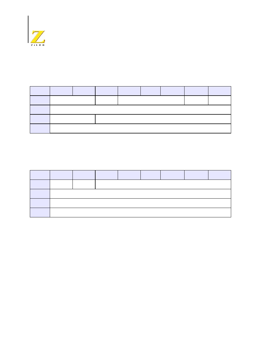
PS024604-1005
P R E L I M I N A R Y
Appendix A--Register Tables
Z8 Encore!
�
Motor Control Flash MCUs
Product Specification
340
Hex Address: F63
Hex Address: F64
Hex Address: F65
Reserved
SPI Mode Register (SPIMODE)
BITS
7
6
5
4
3
2
1
0
FIELD
Reserved
DIAG
NUMBITS[2:0]
SSIO
SSV
RESET
00H
R/W
R
R/W
ADDR
F63H
SPI Diagnostic State Register (SPIDST)
BITS
7
6
5
4
3
2
1
0
FIELD
SCKEN
TCKEN
SPISTATE
RESET
00H
R/W
R
ADDR
F64H

PS024604-1005
P R E L I M I N A R Y
Appendix A--Register Tables
Z8FMC16100 Series Flash MCU
Product Specification
341
Hex Address: F66
Hex Address: F67
Hex Addresses: F68�F6F
Reserved
SPI Baud Rate High Byte Register (SPIBRH)
BITS
7
6
5
4
3
2
1
0
FIELD
BRH
RESET
FFH
R/W
R/W
ADDR
F66H
SPI Baud Rate Low Byte Register (SPIBRL)
BITS
7
6
5
4
3
2
1
0
FIELD
BRL
RESET
FFH
R/W
R/W
ADDR
F67H

PS024604-1005
P R E L I M I N A R Y
Appendix A--Register Tables
Z8 Encore!
�
Motor Control Flash MCUs
Product Specification
342
Analog-to-Digital Converter (ADC)
Hex Address: F70
ADC Control Register 0 (ADCCT0)
BITS
7
6
5
4
3
2
1
0
FIELD
START
Reserved
REFEN
ADCEN
Reserved
ANAIN[2:0]
RESET
0
0
0
0
0
0
0
0
R/W
R/W1
R/W
R/W
R/W
R/W
R/W
R/W
R/W
ADDR
F70H
Bit
Position
Value
(H)
Description
[7]
START
0
ADC Start / Busy
Writing to 0 has no effect.
Reading a 0 indicates the ADC is available to begin a conversion.
1
Writing to 1 starts a conversion.
Reading a 1 indicates a conversion is currently in progress.
[6]
0
Reserved--Must Be 0.
[5]
REFEN
0
Reference Enable
Internal reference voltage is disabled allowing an external reference voltage to be
used by the ADC.
1
Internal reference voltage for the ADC is enabled. The internal reference voltage
can be measured on the VREF pin.
[4]
ADCEN
0
ADC Enable
ADC is disabled for low power operation.
1
ADC is enabled for normal use.
[3]
Reserved
0
Reserved--Must Be 0.
PS024604-1005
P R E L I M I N A R Y
Appendix A--Register Tables
Z8FMC16100 Series Flash MCU
Product Specification
343
Hex Address: F71
[2:0]
ANAIN
000
Analog Input Select
ANA0 input is selected for analog to digital conversion.
001
ANA1 input is selected for analog to digital conversion.
010
ANA2 input is selected for analog to digital conversion.
011
ANA3 input is selected for analog to digital conversion.
100
ANA4 input is selected for analog to digital conversion.
101
ANA5 input is selected for analog to digital conversion.
110
ANA6 input is selected for analog to digital conversion.
111
ANA7 input is selected for analog to digital conversion.
ADC Raw Data High Byte Register (ADCRD_H)
BITS
7
6
5
4
3
2
1
0
FIELD
ADCRDH
RESET
X
R/W
R
ADDR
F71H
Bit
Position
Value
(H)
Description
[7:0]
00H�FFH ADC Raw Data High Byte
The data in this register is the raw data coming from the SAR Block. It will change
as the conversion is in progress. This register is used for testing only.

PS024604-1005
P R E L I M I N A R Y
Appendix A--Register Tables
Z8 Encore!
�
Motor Control Flash MCUs
Product Specification
344
Hex Address: F72
Hex Address: F73
ADC Raw Data High Byte Register (ADCRD_H)
BITS
7
6
5
4
3
2
1
0
FIELD
ADCRDH
RESET
X
R/W
R
ADDR
F71H
Bit
Position
Value
(H)
Description
[7:0]
00H�FFH ADC Raw Data High Byte
The data in this register is the raw data coming from the SAR Block. It will change
as the conversion is in progress. This register is used for testing only.
ADC Data Low Bits Register (ADCD_L)
BITS
7
6
5
4
3
2
1
0
FIELD
ADCDL
Reserved
RESET
X
X
R/W
R
R
ADDR
F73H
Bit
Position
Value
(H)
Description
[7:6]
00�11b
ADC Low Bits
These bits are the 2 least significant bits of the 10-bit ADC output. These bits are
undefined after a Reset. The low bits are latched into this register whenever the
ADC Data High Byte register is read.
[5:0]
Reserved
0
Reserved--Must Be 0.

PS024604-1005
P R E L I M I N A R Y
Appendix A--Register Tables
Z8FMC16100 Series Flash MCU
Product Specification
345
Hex Address: F74
Hex Address: F75
Sample and Settling Time (ADCSST)
BITS
7
6
5
4
3
2
1
0
FIELD
Reserved
SST
RESET
0
1
1
1
1
R/W
R
R/W
ADDR
F74H
Bit
Position
Value
(H)
Description
[7:4]
0H
Reserved - Must be 0.
[3:0]
SST
0H - FH
Sample settling time in number of system clock periods to meet 0.5uS minimum.
Sample Hold Time (ADCST)
BITS
7
6
5
4
3
2
1
0
FIELD
Reserved
ST
RESET
0
1
1
1
1
1
1
R/W
R/W
R/W
ADDR
F75H
Bit
Position
Value
(H)
Description
[7:5]
0H
Reserved - Must be 0.
[4:0]
SHT
0H - FH
Sample Hold time in number of system clock periods to meet 1uS minimum.

PS024604-1005
P R E L I M I N A R Y
Appendix A--Register Tables
Z8 Encore!
�
Motor Control Flash MCUs
Product Specification
346
Hex Address: F76
Hex Addresses: F77�F85
Reserved
ADC Clock Prescale Register (ADCCP)
BITS
7
6
5
4
3
2
1
0
FIELD
Reserved
DIV16
DIV8
DIV4
DIV2
RESET
0
0
0
0
0
R/W
R/W
ADDR
F76H
Bit
Position
Value
(H)
Description
[0]
DIV2
0
DIV2
Clock is not divided
1
System Clock is divided by 2 for ADC Clock
[1]
DIV4
0
DIV4
Clock is not divided
1
System Clock is divided by 4 for ADC Clock
[2]
DIV8
0
DIV8
Clock is not divided
1
System Clock is divided by 8 for ADC Clock
[3]
DIV16
0
DIV16
Clock is not divided
1
System Clock is divided by 16 for ADC Clock
[7:4]
0H
Reserved - must be 0.

PS024604-1005
P R E L I M I N A R Y
Appendix A--Register Tables
Z8FMC16100 Series Flash MCU
Product Specification
347
Oscillator Control
Hex Address: F86
Oscillator Control Register (OSCCTL)
BITS
7
6
5
4
3
2
1
0
FIELD
INTEN
XTLEN
WDTEN
POFEN
WDFEN
FLPEN
SCKSEL
RESET
1
0
1
0
0
0*
00
R/W
R/W
R/W
R/W
R/W
R/W
R/W
R/W
ADDR
F86H
* The reset value is 1 if the option bit LPDEN is 0.
Bit
Position
Value
(H)
Description
[7]
INTEN
0
Internal Precision Oscillator Enable
Internal precision oscillator is disabled.
1
Internal precision oscillator is enabled.
[6]
XTLEN
0
Crystal Oscillator Enable
Crystal oscillator is disabled.
1
Crystal oscillator is enabled.
[5]
WDTEN
0
Watch-Dog Timer Oscillator Enable
Watch-Dog Timer oscillator is disabled
1
Watch-Dog Timer oscillator is enabled
[4]
POFEN
0
Primary Oscillator Failure Detection Enable
Failure detection and recovery of primary oscillator is disabled. This bit is cleared
automatically if a primary oscillator failure is detected.
1
Failure detection and recovery of primary oscillator is enabled
[3]
WDFEN
0
Watch-Dog Timer Oscillator Failure Detection Enable
Failure detection of Watch-Dog Timer oscillator is disabled.This bit is cleared
automatically if a Watch-Dog Timer oscillator failure is detected.
1
Failure detection of Watch-Dog Timer oscillator is enabled

PS024604-1005
P R E L I M I N A R Y
Appendix A--Register Tables
Z8 Encore!
�
Motor Control Flash MCUs
Product Specification
348
Hex Address: F87
Trim Control
Hex Addresses: F88�F8F
Reserved
[2]
FLPEN
0
Flash Low Power Mode Enable
Flash Low Power Mode is disabled.
1
Flash Low Power Mode is enabled. The Flash will be powered down during idle
periods of the clock and powered up during Flash reads. This bit should only be
set if the frequency of the primary oscillator source is 8MHz or lower. The reset
value of this bit is controlled by the LPDEN option bit during reset.
[1:0]
SCKSEL
00
01
10
11
System Clock Oscillator Select
Internal precision oscillator functions as system clock at 5.6MHz
Reserved
Crystal oscillator or external clock driver functions as system clock
Watch-Dog Timer oscillator functions as system clock
Oscillator Divide Register (OSCDIV)
BITS
7
6
5
4
3
2
1
0
FIELD
DIV
RESET
00H*
R/W
R/W
ADDR
F87H
* The reset value is 08H if the option bit LPDEN is 0.
Bit
Position
Value
(H)
Description
[7:0]
DIV
00H to
FFH
Oscillator Divide
00H - divider is disabled, all other entries are the divide value for scaling the
system clock.
Bit
Position
Value
(H)
Description

PS024604-1005
P R E L I M I N A R Y
Appendix A--Register Tables
Z8FMC16100 Series Flash MCU
Product Specification
349
Comparator and Op Amp
Hex Address: F90
Comparator and Op Amp Control Register (CMPOPC)
BITS
7
6
5
4
3
2
1
0
FIELD
OPEN
Reserved
CPSEL
CMPIRQ
CMPIV
CMPOUT
CMPEN
RESET
0
00
0
0
0
X
0
R/W
R/W
R/W
R/W
R/W
R/W
R
R/W
ADDR
F90H
Bit
Position
Value
(H)
Description
[7]
OPEN
0
Operational Amplifier Disable
Operational amplifier is disabled.
1
Operational amplifier is enabled.
[6:5]
Reserved
Must be 0.
[3]
CPSEL
0
Comparator Input Select
Comparator input is PA1
1
Comparator input is PB4
[3]
CMPIRQ
0
Comparator Interrupt Edge Select
Interrupt Request on Comparator Rising Edge
1
Interrupt Request on Comparator Falling Edge
[2]
CMPIV
0
PWM Fault Comparator Polarity
PWM Fault is active when cp+ > cp-
1
PWM Fault is active when cp- > cp+
[1]
CMPOUT
0
Comparator Output Value
Comparator output is logical 0.
1
Comparator output is logical 1.
[0]
CMPEN
0
Comparator Enable
Comparator is disabled.
1
Comparator is enabled.

PS024604-1005
P R E L I M I N A R Y
Appendix A--Register Tables
Z8 Encore!
�
Motor Control Flash MCUs
Product Specification
350
Hex Addresses: F91�FBF
Reserved
Interrupt Controller
Hex Address: FC0
Interrupt Request 0 Register (IRQ0)
BITS
7
6
5
4
3
2
1
0
FIELD
PWMI
FLTI
ADCI
CMPI
T0I
U0RXI
U0TXI
SPII
RESET
0
0
0
0
0
0
0
0
R/W
R/W
R/W
R/W
R/W
R/W
R/W
R/W
R/W
ADDR
FC0H
Bit
Position
Value
(H)
Description
[7]
PWMI
0
PWM Timer Interrupt Request
No interrupt request is pending for the Pulse-Width Modulator.
1
An interrupt request from the Pulse-Width Modulator is awaiting service.
[6]
FLTI
0
Fault Interrupt Request. The fault interrupt is generated in the PWM module and
originates from the Fault0 pin, Fault1 pin or the Comparator output. An interrupt
enable for each of these sources exists in the PWM module.
No Fault interrupt request is pending.
1
A Fault interrupt request is awaiting service.
[5]
ADCI
0
ADC Interrupt Request
No interrupt request is pending for the Analog to Digital Converter.
1
An interrupt request from the Analog to Digital Converter is awaiting service.
[4]
CMPI
0
Comparator Interrupt Request
No interrupt request is pending for the Comparators.
1
An interrupt request from the Comparators is awaiting service.
[3]
T0I
0
Timer 0 Interrupt Request
No interrupt request is pending for Timer 0.
1
An interrupt request from Timer 0 is awaiting service.
PS024604-1005
P R E L I M I N A R Y
Appendix A--Register Tables
Z8FMC16100 Series Flash MCU
Product Specification
351
Hex Address: FC1
Hex Address: FC2
[2]
U0RXI
0
UART 0 Receiver Interrupt Request
No interrupt request is pending for the UART 0 receiver.
1
An interrupt request from the UART 0 receiver is awaiting service.
[1]
U0TXI
0
UART 0 Transmitter Interrupt Request
No interrupt request is pending for the UART 0 transmitter.
1
An interrupt request from the UART 0 transmitter is awaiting service.
[0]
SPII
0
SPI Interrupt Request
No interrupt request is pending for the SPI.
1
An interrupt request from the SPI is awaiting service.
IRQ0 Enable High Bit Register (IRQ0ENH)
BITS
7
6
5
4
3
2
1
0
FIELD
PWMENH
FLTENH
ADCENH CMPENH
T0ENH
U0RENH
U0TENH
SPIENH
RESET
0
0
0
0
0
0
0
0
R/W
R/W
R/W
R/W
R/W
R/W
R/W
R/W
R/W
ADDR
FC1H
IRQ0 Enable Low Bit Register (IRQ0ENL)
BITS
7
6
5
4
3
2
1
0
FIELD
PWMENL
FLTENL
ADCENL
CMPENL
T0ENL
U0RENL
U0TENL
SPIENL
RESET
0
0
0
0
0
0
0
0
R/W
R/W
R/W
R/W
R/W
R/W
R/W
R/W
R/W
ADDR
FC2H
Bit
Position
Value
(H)
Description

PS024604-1005
P R E L I M I N A R Y
Appendix A--Register Tables
Z8 Encore!
�
Motor Control Flash MCUs
Product Specification
352
Hex Address: FC3
Interrupt Request 1 Register (IRQ1)
BITS
7
6
5
4
3
2
1
0
FIELD
I2CI
Reserved
PC0I
PBI
PA73I
PA62I
PA51I
PA40I
RESET
0
0
0
0
0
0
0
0
R/W
R/W
R
R/W
R/W
R/W
R/W
R/W
R/W
ADDR
FC3H
Bit
Position
Value
(H)
Description
[7]
I2CI
0
I2C Interrupt Request
No interrupt request is pending for I2C.
1
An interrupt request from I2C is awaiting service.
[5]
PC0I
0
PC0 Interrupt Request -- Logic in the Port C GPIO module selects either the
rising or falling edge.
No interrupt request is pending for PC0.
1
An interrupt request from PC0 is awaiting service.
[4]
PBI
0
PB3 � PB0 Interrupt Request
No interrupt request is pending for any PB3 � PB0.
1
An interrupt request from PB3 � PB0 is awaiting service.
[3]
PA73I
0
PA7 or PA3 Interrupt Request -- Logic in the Port A GPIO module selects either
PA7 or PA3 and either rising or falling edge.
No interrupt request is pending for PA7 or PA3
1
An interrupt request from PA7 or PA3 is awaiting service.
[2]
PA62I
0
PA6 or PA2 Interrupt Request -- Logic in the Port A GPIO module selects either
PA6 or PA2 and either rising or falling edge.
No interrupt request is pending for PA6 or PA2
1
An interrupt request from PA6 or PA2 is awaiting service.
[1]
PA51I
0
PA5 or PA1 Interrupt Request -- Logic in the Port A GPIO module selects either
PA5 or PA1 and either rising or falling edge.
No interrupt request is pending for PA5 or PA1
1
An interrupt request from PA5 or PA1 is awaiting service.
[0]
PA40I
0
PA4 or PA0 Interrupt Request -- Logic in the Port A GPIO module selects either
PA4 or PA0 and either rising or falling edge.
No interrupt request is pending for PA4 or PA0
1
An interrupt request from PA4 or PA0 is awaiting service.
PS024604-1005
P R E L I M I N A R Y
Appendix A--Register Tables
Z8FMC16100 Series Flash MCU
Product Specification
353
Hex Address: FC4
Hex Address: FC5
IRQ1 Enable High Bit Register (IRQ1ENH)
BITS
7
6
5
4
3
2
1
0
FIELD
I2CENH
Reserved
PC0ENH
PBENH
PA73ENH PA62ENH PA51ENH PA40ENH
RESET
0
0
0
0
0
0
0
0
R/W
R/W
R
R/W
R/W
R/W
R/W
R/W
R/W
ADDR
FC4H
Bit
Position
Name
Description
[7]
I2CENH
I2C Interrupt Request Enable High Bit
[5]
PC0ENH Port C0Interrupt Request Enable High Bit
[4]
PBENH
Port B[3:0] Interrupt Request Enable High Bit
[3]
PA73ENH Port A73 Interrupt Request Enable High Bit
[2]
PA62ENH Port A62 Interrupt Request Enable High Bit
[1]
PA51ENH Port A51 Interrupt Request Enable High Bit
[0]
PA40ENH Port A40 Interrupt Request Enable High Bit
IRQ1 Enable Low Bit Register (IRQ1ENL)
BITS
7
6
5
4
3
2
1
0
FIELD
I2CENL
Reserved
PC0ENL
PBENL
PA73ENL PA62ENL PA51ENL PA40ENL
RESET
0
0
0
0
0
0
0
0
R/W
R/W
R
R/W
R/W
R/W
R/W
R/W
R/W
ADDR
FC5H
PS024604-1005
P R E L I M I N A R Y
Appendix A--Register Tables
Z8 Encore!
�
Motor Control Flash MCUs
Product Specification
354
Hex Addresses: FC9�FCE
Reserved
Hex Address: FCF
Bit
Position
Name
Description
[7]
I2CENL
I2C Interrupt Request Enable Low Bit
[5]
PC0ENL Port C0Interrupt Request Enable Low Bit
[4]
PBENL
Port B[3:0] Interrupt Request Enable Low Bit
[3]
PA73ENL Port A73 Interrupt Request Enable Low Bit
[2]
PA62ENL Port A62 Interrupt Request Enable Low Bit
[1]
PA51ENL Port A51 Interrupt Request Enable Low Bit
[0]
PA40ENL Port A40 Interrupt Request Enable Low Bit
Interrupt Control Register (IRQCTL)
BITS
7
6
5
4
3
2
1
0
FIELD
IRQE
Reserved
RESET
0
0
0
0
0
0
0
0
R/W
R/W
R
R
R
R
R
R
R
ADDR
FCFH

PS024604-1005
P R E L I M I N A R Y
Appendix A--Register Tables
Z8FMC16100 Series Flash MCU
Product Specification
355
GPIO Port A
Hex Address: FD0
Hex Address: FD1
Hex Address: FD2
Port A�C GPIO Address Registers (PxADDR)
BITS
7
6
5
4
3
2
1
0
FIELD
PADDR[7:0]
RESET
00H
R/W
R/W
ADDR
FD0H, FD4H, FD8H
Port A�C Control Registers (PxCTL)
BITS
7
6
5
4
3
2
1
0
FIELD
PCTL
RESET
00H
R/W
R/W
ADDR
FD1H, FD5H, FD9H
Port A-C Input Data Registers (PxIN)
BITS
7
6
5
4
3
2
1
0
FIELD
PIN7
PIN6
PIN5
PIN4
PIN3
PIN2
PIN1
PIN0
RESET
X
X
X
X
X
X
X
X
R/W
R
R
R
R
R
R
R
R
ADDR
FD2H, FD6H, FDAH
Bit
Position
Value
(H)
Description
[7:0]
PIN
0
Port Input Data x
Input data is a logical 0 (Low).
1
Input data is a logical 1 (High).

PS024604-1005
P R E L I M I N A R Y
Appendix A--Register Tables
Z8 Encore!
�
Motor Control Flash MCUs
Product Specification
356
Hex Address: FD3
GPIO Port B
Hex Address: FD4
Port A-C Output Data Register (PxOUT)
BITS
7
6
5
4
3
2
1
0
FIELD
POUT7
POUT6
POUT5
POUT4
POUT3
POUT2
POUT1
POUT0
RESET
0
0
0
0
0
0
0
0
R/W
R/W
R/W
R/W
R/W
R/W
R/W
R/W
R/W
ADDR
FD3H, FD7H, FDBH
Bit
Position
Value
(H)
Description
[7:0]
POUT
0
Port Output Data x
Drive is a logical 0 (Low).
1
Drive is a logical 1 (High). High value is not driven if the drain has been disabled
by setting the corresponding Port Output Control register bit to 1.
Port A�C GPIO Address Registers (PxADDR)
BITS
7
6
5
4
3
2
1
0
FIELD
PADDR[7:0]
RESET
00H
R/W
R/W
ADDR
FD0H, FD4H, FD8H

PS024604-1005
P R E L I M I N A R Y
Appendix A--Register Tables
Z8FMC16100 Series Flash MCU
Product Specification
357
Hex Address: FD5
Hex Address: FD6
Hex Address: FD7
Port A�C Control Registers (PxCTL)
BITS
7
6
5
4
3
2
1
0
FIELD
PCTL
RESET
00H
R/W
R/W
ADDR
FD1H, FD5H, FD9H
Port A-C Input Data Registers (PxIN)
BITS
7
6
5
4
3
2
1
0
FIELD
PIN7
PIN6
PIN5
PIN4
PIN3
PIN2
PIN1
PIN0
RESET
X
X
X
X
X
X
X
X
R/W
R
R
R
R
R
R
R
R
ADDR
FD2H, FD6H, FDAH
Bit
Position
Value
(H)
Description
[7:0]
PIN
0
Port Input Data x
Input data is a logical 0 (Low).
1
Input data is a logical 1 (High).
Port A-C Output Data Register (PxOUT)
BITS
7
6
5
4
3
2
1
0
FIELD
POUT7
POUT6
POUT5
POUT4
POUT3
POUT2
POUT1
POUT0
RESET
0
0
0
0
0
0
0
0
R/W
R/W
R/W
R/W
R/W
R/W
R/W
R/W
R/W
ADDR
FD3H, FD7H, FDBH
PS024604-1005
P R E L I M I N A R Y
Appendix A--Register Tables
Z8 Encore!
�
Motor Control Flash MCUs
Product Specification
358
GPIO Port C
Hex Address: FD8
Hex Address: FD9
Bit
Position
Value
(H)
Description
[7:0]
POUT
0
Port Output Data x
Drive is a logical 0 (Low).
1
Drive is a logical 1 (High). High value is not driven if the drain has been disabled
by setting the corresponding Port Output Control register bit to 1.
Port A�C GPIO Address Registers (PxADDR)
BITS
7
6
5
4
3
2
1
0
FIELD
PADDR[7:0]
RESET
00H
R/W
R/W
ADDR
FD0H, FD4H, FD8H
Port A�C Control Registers (PxCTL)
BITS
7
6
5
4
3
2
1
0
FIELD
PCTL
RESET
00H
R/W
R/W
ADDR
FD1H, FD5H, FD9H
PS024604-1005
P R E L I M I N A R Y
Appendix A--Register Tables
Z8FMC16100 Series Flash MCU
Product Specification
359
Hex Address: FDA
Hex Address: FDB
Port A-C Input Data Registers (PxIN)
BITS
7
6
5
4
3
2
1
0
FIELD
PIN7
PIN6
PIN5
PIN4
PIN3
PIN2
PIN1
PIN0
RESET
X
X
X
X
X
X
X
X
R/W
R
R
R
R
R
R
R
R
ADDR
FD2H, FD6H, FDAH
Bit
Position
Value
(H)
Description
[7:0]
PIN
0
Port Input Data x
Input data is a logical 0 (Low).
1
Input data is a logical 1 (High).
Port A-C Output Data Register (PxOUT)
BITS
7
6
5
4
3
2
1
0
FIELD
POUT7
POUT6
POUT5
POUT4
POUT3
POUT2
POUT1
POUT0
RESET
0
0
0
0
0
0
0
0
R/W
R/W
R/W
R/W
R/W
R/W
R/W
R/W
R/W
ADDR
FD3H, FD7H, FDBH
Bit
Position
Value
(H)
Description
[7:0]
POUT
0
Port Output Data x
Drive is a logical 0 (Low).
1
Drive is a logical 1 (High). High value is not driven if the drain has been disabled
by setting the corresponding Port Output Control register bit to 1.
PS024604-1005
P R E L I M I N A R Y
Appendix A--Register Tables
Z8 Encore!
�
Motor Control Flash MCUs
Product Specification
360
Reset and Watch-Dog Timer (WDT)
Hex Address: FF0
Hex Address: FF1
Reserved
Hex Address: FF2
Reset Status and Control Register (RSTSCR)
BITS
7
6
5
4
3
2
1
0
FIELD
POR
STOP
WDT
EXT
FLT
Reserved
FLTSEL
RESET
See Table 10.
0
R/W
R
R
R
R
R
R
R/W
ADDR
FF0H
Watch-Dog Timer Reload High Byte Register (WDTH)
BITS
7
6
5
4
3
2
1
0
FIELD
WDTH
RESET
04H
R/W
R/W*
ADDR
FF2H
R/W* - Read returns the current WDT count value. Write sets the desired Reload Value.
PS024604-1005
P R E L I M I N A R Y
Appendix A--Register Tables
Z8FMC16100 Series Flash MCU
Product Specification
361
Hex Address: FF3
Hex Addresses: FF4�FF5
Reserved
Hex Address: FF6
Watch-Dog Timer Reload Low Byte Register (WDTL)
BITS
7
6
5
4
3
2
1
0
FIELD
WDTL
RESET
00H
R/W
R/W*
ADDR
FF3H
R/W* - Read returns the current WDT count value. Write sets the desired Reload Value.
Trim Bit Address Register (TRMADR)
BITS
7
6
5
4
3
2
1
0
FIELD
TRMADR
RESET
00H
R/W
R/W
ADDR
FF6H
Bit Position Value (H) Description
[7:0}
TRMADR
00 - 1FH Trim Bit Address Register
PS024604-1005
P R E L I M I N A R Y
Appendix A--Register Tables
Z8 Encore!
�
Motor Control Flash MCUs
Product Specification
362
Hex Address: FF7
Flash Memory Controller
Hex Address: FF8
Trim Bit Data Register (TRMDR)
BITS
7
6
5
4
3
2
1
0
FIELD
TRMDR
RESET
00H
R/W
R/W
ADDR
FF7H
Bit Position Value (H) Description
[7:0}
TRMDR
00 - FFH Trim Bit Data Register
Flash Control Register (FCTL)
BITS
7
6
5
4
3
2
1
0
FIELD
FCMD
RESET
00H
R/W
W
ADDR
FF8H
Bit
Position
Value
Description
[7:0]
FCMD
73H
8CH
95H
63H
5EH
Flash Command:
First unlock command.
Second unlock command.
Page erase command.
Mass erase command.
Flash Sector Protect register select.
All other commands, or any command out of sequence, locks the Flash
Controller.

PS024604-1005
P R E L I M I N A R Y
Appendix A--Register Tables
Z8FMC16100 Series Flash MCU
Product Specification
363
Hex Address: FF9
Flash Status Register (FSTAT)
BITS
7
6
5
4
3
2
1
0
FIELD
Reserved
FSTAT
RESET
00B
00_0000B
R/W
R
R
ADDR
FF8H
Bit
Position
Value
Description
[7:6]
Reserved
Must be 00.
[5:0]
FSTAT
00_0000
00_0001
00_0010
00_0011
00_0100
00_1xxx
01_0xxx
10_0xxx
Flash Controller Status
Flash Controller locked.
First unlock command received.
Second unlock command received.
Flash Controller unlocked.
Flash Sector Protect register selected.
Program operation in progress.
Page erase operation in progress.
Mass erase operation in progress.
Flash Status Register (FSTAT)
BITS
7
6
5
4
3
2
1
0
FIELD
Reserved
FSTAT
RESET
00B
00_0000B
R/W
R
R
ADDR
FF8H
PS024604-1005
P R E L I M I N A R Y
Appendix A--Register Tables
Z8 Encore!
�
Motor Control Flash MCUs
Product Specification
364
Bit
Position
Value
Description
[7:6]
Reserved
Must be 00.
[5:0]
FSTAT
00_0000
00_0001
00_0010
00_0011
00_0100
00_1xxx
01_0xxx
10_0xxx
Flash Controller Status
Flash Controller locked.
First unlock command received.
Second unlock command received.
Flash Controller unlocked.
Flash Sector Protect register selected.
Program operation in progress.
Page erase operation in progress.
Mass erase operation in progress.
Flash Sector Protect Register (FPROT)
BITS
7
6
5
4
3
2
1
0
FIELD
SECT7
SECT6
SECT5
SECT4
SECT3
SECT2
SECT1
SECT0
RESET
0
0
0
0
0
0
0
0
R/W
R/W1
R/W1
R/W1
R/W1
R/W1
R/W1
R/W1
R/W1
ADDR
FF9H
R/W1 = Register is accessible for Read operations. Register can be written to 1 only (through user code).
Bit
Position
Value
Description
[7:0]]
SECTn
0
Sector Protect
Sector n can be programmed or erased from user code.
1
Sector n is protected and cannot be programmed or erased from user code.

PS024604-1005
P R E L I M I N A R Y
Appendix A--Register Tables
Z8FMC16100 Series Flash MCU
Product Specification
365
Hex Address: FFA
Hex Address: FFB
.
eZ8 CPU
Refer to the eZ8 CPU User Manual (UM0128).
Op Code Maps
The following two figures provide information about each of the eZ8 CPU instructions.
Flash Frequency High Byte Register (FFREQH)
BITS
7
6
5
4
3
2
1
0
FIELD
FFREQH
RESET
00H
R/W
R/W
ADDR
FFAH
Flash Frequency Low Byte Register (FFREQL)
BITS
7
6
5
4
3
2
1
0
FIELD
FFREQL
RESET
00H
R/W
R/W
ADDR
FFBH

PS024604-1005
P R E L I M I N A R Y
Appendix A--Register Tables
Z8 Encore!
�
Motor Control Flash MCUs
Product Specification
366
First Op Code Map
CP
3.3
R2,R1
CP
3.4
IR2,R1
CP
2.3
r1,r2
CP
2.4
r1,Ir2
CPX
4.3
ER2,ER1
CPX
4.3
IM,ER1
CP
3.3
R1,IM
CP
3.4
IR1,IM
RRC
2.2
R1
RRC
2.3
IR1
0
1
2
3
4
5
6
7
8
9
A
B
C
D
E
F
0
1
2
3
4
5
6
7
8
9
A
B
C
D
E
F
Lower Nibble (Hex)
Up
per
Ni
bbl
e (
H
ex
)
BRK
1.1
SRP
2.2
IM
ADD
2.3
r1,r2
ADD
2.4
r1,Ir2
ADD
3.3
R2,R1
ADD
3.4
IR2,R1
ADD
3.3
R1,IM
ADD
3.4
IR1,IM
ADDX
4.3
ER2,ER1
ADDX
4.3
IM,ER1
DJNZ
2.3
r1,X
JR
2.2
cc,X
LD
2.2
r1,IM
JP
3.2
cc,DA
INC
1.2
r1
NOP
1.2
RLC
2.2
R1
RLC
2.3
IR1
ADC
2.3
r1,r2
ADC
2.4
r1,Ir2
ADC
3.3
R2,R1
ADC
3.4
IR2,R1
ADC
3.3
R1,IM
ADC
3.4
IR1,IM
ADCX
4.3
ER2,ER1
ADCX
4.3
IM,ER1
INC
2.2
R1
INC
2.3
IR1
SUB
2.3
r1,r2
SUB
2.4
r1,Ir2
SUB
3.3
R2,R1
SUB
3.4
IR2,R1
SUB
3.3
R1,IM
SUB
3.4
IR1,IM
SUBX
4.3
ER2,ER1
SUBX
4.3
IM,ER1
DEC
2.2
R1
DEC
2.3
IR1
SBC
2.3
r1,r2
SBC
2.4
r1,Ir2
SBC
3.3
R2,R1
SBC
3.4
IR2,R1
SBC
3.3
R1,IM
SBC
3.4
IR1,IM
SBCX
4.3
ER2,ER1
SBCX
4.3
IM,ER1
DA
2.2
R1
DA
2.3
IR1
OR
2.3
r1,r2
OR
2.4
r1,Ir2
OR
3.3
R2,R1
OR
3.4
IR2,R1
OR
3.3
R1,IM
OR
3.4
IR1,IM
ORX
4.3
ER2,ER1
ORX
4.3
IM,ER1
POP
2.2
R1
POP
2.3
IR1
AND
2.3
r1,r2
AND
2.4
r1,Ir2
AND
3.3
R2,R1
AND
3.4
IR2,R1
AND
3.3
R1,IM
AND
3.4
IR1,IM
ANDX
4.3
ER2,ER1
ANDX
4.3
IM,ER1
COM
2.2
R1
COM
2.3
IR1
TCM
2.3
r1,r2
TCM
2.4
r1,Ir2
TCM
3.3
R2,R1
TCM
3.4
IR2,R1
TCM
3.3
R1,IM
TCM
3.4
IR1,IM
TCMX
4.3
ER2,ER1
TCMX
4.3
IM,ER1
PUSH
2.2
R2
PUSH
2.3
IR2
TM
2.3
r1,r2
TM
2.4
r1,Ir2
TM
3.3
R2,R1
TM
3.4
IR2,R1
TM
3.3
R1,IM
TM
3.4
IR1,IM
TMX
4.3
ER2,ER1
TMX
4.3
IM,ER1
DECW
2.5
RR1
DECW
2.6
IRR1
LDE
2.5
r1,Irr2
LDEI
2.8
Ir1,Irr2
LDX
3.2
r1,ER2
LDX
3.3
Ir1,ER2
LDX
3.4
IRR2,R1
LDX
3.5
IRR2,IR1
LDX
3
3.4
r1,rr2,X
LDX
3
3.4
rr1,r2,X
RL
2.2
R1
RL
2.3
IR1
LDE
2.5
r2,Irr1
LDEI
2.8
Ir2,Irr1
LDX
3.2
r2,ER1
LDX
3.3
Ir2,ER1
LDX
3.4
R2,IRR1
LDX
3.5
IR2,IRR1
LEA
3.3
r1,r2,X
LEA
3
3.5
rr1,rr2,X
INCW
2.5
RR1
INCW
2.6
IRR1
CLR
2.2
R1
CLR
2.3
IR1
XOR
2.3
r1,r2
XOR
2.4
r1,Ir2
XOR
3.3
R2,R1
XOR
3.4
IR2,R1
XOR
3.3
R1,IM
XOR
3.4
IR1,IM
XORX
4.3
ER2,ER1
XORX
4.3
IM,ER1
LDC
2.5
r1,Irr2
LDCI
2.8
Ir1,Irr2
LDC
2.5
r2,Irr1
LDCI
2.8
Ir2,Irr1
JP
2
2.3
IRR1
LDC
2.8
Ir1,Irr2
LD
3.4
r1,r2,X
PUSHX
3
3.3
ER2
SRA
2.2
R1
SRA
2.3
IR1
POPX
3
3.3
ER1
LD
3.4
r2,r1,X
CALL
2
2.6
IRR1
BSWAP
2.2
R1
CALL
3.3
DA
LD
3.2
R2,R1
LD
3.3
IR2,R1
BIT
2.2
p,b,r1
LD
2.3
r1,Ir2
LDX
4.2
ER2,ER1
LDX
4.2
IM,ER1
LD
3.3
R1,IM
LD
3.4
IR1,IM
RR
2.2
R1
RR
2.3
IR1
MULT
2.9
RR1
LD
3.3
R2,IR1
TRAP
2.6
Vector
LD
2.3
Ir1,r2
BTJ
3.3
p,b,r1,X
BTJ
3.4
p,b,Ir1,X
SWAP
2.2
R1
SWAP
2.3
IR1
RCF
1.2
WDT
1.2
STOP
1.2
HALT
1.2
DI
1.2
EI
1.2
RET
1.4
IRET
1.5
SCF
1.2
CCF
1.2
Op Code
See 2nd
Map
ATM
1.1

PS024604-1005
P R E L I M I N A R Y
Appendix A--Register Tables
Z8FMC16100 Series Flash MCU
Product Specification
367
Second Op Code Map After 1Fh
CPC
4.3
R2,R1
CPC
4.4
IR2,R1
CPC
3.3
r1,r2
CPC
3.4
r1,Ir2
CPCX
5.3
ER2,ER1
CPCX
5.3
IM,ER1
CPC
4.3
R1,IM
CPC
4.4
IR1,IM
SRL
3.2
R1
SRL
3.3
IR1
0
1
2
3
4
5
6
7
8
9
A
B
C
D
E
F
0
1
2
3
4
5
6
7
8
9
A
B
C
D
E
F
Lower Nibble (Hex)
Up
per
Nib
b
l
e
(
H
ex
)
PUSH
3.2
IM
LDWX
4.2
ER2,ER1

PS024604-1005
P R E L I M I N A R Y
Appendix A--Register Tables
Z8 Encore!
�
Motor Control Flash MCUs
Product Specification
368

Z8FMC16100 Series Flash MCU
Product Specification
PS024604-1005
P R E L I M I N A R Y
Index
369
Index
Symbols
# 280
% 280
@ 280
Numerics
10-bit ADC 4
32-pin QFN and LQFP packages 8
A
absolute maximum ratings 257
AC characteristics 264
ADC 282
block diagram 200
electrical characteristics and timing 267
overview 199
ADC Channel Register 1 (ADCCTL) 203, 342
ADC Data High Byte Register (ADCDH) 204,
205, 208, 209, 314, 315, 343, 344
ADC Data Low Bit Register (ADCDL) 205, 206,
207, 344, 345, 346
ADC Timer Capture Register 208
ADCX 282
ADD 282
add - extended addressing 282
add with carry 282
add with carry--extended addressing 282
additional symbols 280
address space 13
ADDX 282
analog block/PWM signal synchronization 202
analog signals 10
analog-to-digital converter
overview 199
AND 285
ANDX 285
architecture
voltage measurements 199
arithmetic instructions 282
assembly language programming 277
assembly language syntax 278
ATM 285
atomic 285
B
B 280
b 279
baud rate generator, UART 127
BCLR 283
binary number suffix 280
BIT 283
bit 279
clear 283
manipulation instructions 283
set 283
set or clear 283
swap 283
test and jump 285
test and jump if non-zero 285
test and jump if zero 285
bit jump and test if non-zero 285
bit swap 285
block diagram 2
block transfer instructions 283
BRK 285
BSET 283
BSWAP 283, 285
BTJ 285
BTJNZ 285
BTJZ 285
C
calibration and compensation, motor control mea-
surements 203
CALL procedure 285
cc 279

Z8FMC16100 Series Flash MCU
Product Specification
PS024604-1005
P R E L I M I N A R Y
Index
370
CCF 284
Change Log 306
characteristics
pin 11
characteristics, electrical 257
clear 284
clock phase (SPI) 152
CLR 284
COM 285
comparator
definition 195
noninverting/inverting input 195
operation 195
compare - extended addressing 282
compare with carry 282
compare with carry - extended addressing 282
complement 285
complement carry flag 283, 284
condition code 279
control register definition, UART 130
control register, I2C 186
CP 282
CPC 282
CPCX 282
CPU and peripheral overview 3
CPU control instructions 284
CPX 282
current measurement
architecture 199
operation 200
Customer Feedback Form 379
D
DA 279, 282
data register, I2C 184
DC characteristics 258
debugger, on-chip 241
DEC 282
decimal adjust 282
decrement 282
decrement and jump non-zero 285
decrement word 282
DECW 282
destination operand 280
device, port availability 35
DI 284
direct address 279
disable interrupts 284
DJNZ 285
DMA
controller 4
Document Information 305
Document Number Description 305
dst 280
E
EI 284
electrical characteristics 257
ADC 267
GPIO input data sample timing 271
watch-dog timer 267
electrical noise 199
enable interrupt 284
ER 279
extended addressing register 279
external pin reset 27
external RC oscillator 266
eZ8 CPU features 3
eZ8 CPU instruction classes 282
eZ8 CPU instruction notation 279
eZ8 CPU instruction set 277
eZ8 CPU instruction summary 286
F
FCTL register 217, 227, 361, 362
first opcode map 298, 366
FLAGS 280
flags register 280
flash
controller 4
option bit address space 224
option bit configuration - reset 224
program memory address 0000H 224
program memory address 0001H 225

Z8FMC16100 Series Flash MCU
Product Specification
PS024604-1005
P R E L I M I N A R Y
Index
371
flash memory
arrangement 212
byte programming 215
code protection 213
configurations 211
controller bypass 216
flash control register 217, 227, 361, 362
flash status register 218
frequency high and low byte registers 220
mass erase 216
operation 213
operation timing 213
page erase 216
page select register 218
FPS register 218
FSTAT register 218
G
general-purpose I/O 35
GPIO 4, 35
alternate functions 36
architecture 35
control register definitions 39
input data sample timing 271
interrupts 39
port A-C pull-up enable sub-registers 45
port A-H address registers 40
port A-H alternate function sub-registers 42,
47
port A-H control registers 41
port A-H data direction sub-registers 41
port A-H high drive enable sub-registers 44
port A-H input data registers 48
port A-H output control sub-registers 43
port A-H output data registers 49
port A-H STOP mode recovery sub-registers
44
port availability by device 35
port input timing 271
port output timing 272
H
H 280
HALT 284
halt mode 31, 284
hexadecimal number prefix/suffix 280
I
I2C 4
10-bit address read transaction 175
10-bit address transaction 172
10-bit addressed slave data transfer format
172, 180
7-bit address transaction 169, 177
7-bit address, reading a transaction 174
7-bit addressed slave data transfer format 171,
179
7-bit receive data transfer format 175, 181,
182
baud high and low byte registers 187, 188,
193
C status register 185, 189, 336, 337
controller 163
interrupts 167
operation 166
SDA and SCL signals 166
stop and start conditions 169
I2CBRH register 188, 190, 192, 193, 337, 338
I2CBRL register 188, 337
I2CCTL register 186, 336
I2CDATA register 184, 336
I2CSTAT register 185, 189, 336, 337
IM 279
immediate data 279
immediate operand prefix 280
INC 282
increment 282
increment word 282
INCW 282
indexed 280
indirect address prefix 280
indirect register 279
indirect register pair 279
indirect working register 279

Z8FMC16100 Series Flash MCU
Product Specification
PS024604-1005
P R E L I M I N A R Y
Index
372
indirect working register pair 279
infrared encoder/decoder (IrDA) 145
instruction set, ez8 CPU 277
instructions
ADC 282
ADCX 282
ADD 282
ADDX 282
AND 285
ANDX 285
arithmetic 282
ATM 285
BCLR 283
BIT 283
bit manipulation 283
block transfer 283
BRK 285
BSET 283
BSWAP 283, 285
BTJ 285
BTJNZ 285
BTJZ 285
CALL 285
CCF 283, 284
CLR 284
COM 285
CP 282
CPC 282
CPCX 282
CPU control 284
CPX 282
DA 282
DEC 282
DECW 282
DI 284
DJNZ 285
EI 284
HALT 284
INC 282
INCW 282
IRET 285
JP 285
LD 284
LDC 284
LDCI 283, 284
LDE 284
LDEI 283
LDWX 284
LDX 284
LEA 284
load 284
logical 285
MULT 283
NOP 284
OR 285
ORX 285
POP 284
POPX 284
program control 285
PUSH 284
PUSHX 284
RCF 283, 284
RET 285
RL 285
RLC 286
rotate and shift 285
RR 286
RRC 286
SBC 283
SCF 283, 284
SRA 286
SRL 286
SRP 284
STOP 284
SUB 283
SUBX 283
SWAP 286
TCM 283
TCMX 283
TM 283
TMX 283
TRAP 285
watch-dog timer refresh 284
XOR 285
XORX 285
instructions, eZ8 classes of 282
interrupt control register 61
interrupt controller 4, 51

Z8FMC16100 Series Flash MCU
Product Specification
PS024604-1005
P R E L I M I N A R Y
Index
373
architecture 51
interrupt assertion types 54
interrupt vectors and priority 54
register definitions 55
software interrupt assertion 55
interrupt edge select register 46
Interrupt Port Select Register 47
interrupt request 0 register 55
interrupt request 1 register 57
interrupt return 285
interrupt vector listing 51
interrupts
SPI 156
UART 124
introduction 1
IR 279
Ir 279
IrDA
architecture 128, 145
block diagram 128, 145
control register definitions 148
operation 128, 145
receiving data 147
transmitting data 146
IRET 285
IRQ0 enable high and low bit registers 58
IRQ1 enable high and low bit registers 59
IRR 279
Irr 279
J
JP 285
jump, conditional, relative, and relative conditional
285
L
LD 284
LDC 284
LDCI 283, 284
LDE 284
LDEI 283, 284
LDWX 284
LDX 284
LEA 284
load 284
load constant 283
load constant to/from program memory 284
load constant with auto-increment addresses 284
load effective address 284
load external data 284
load external data to/from data memory and auto-
increment addresses 283
load external to/from data memory and auto-incre-
ment addresses 284
load instructions 284
load using extended addressing 284
load word using extended addressing 284
logical AND 285
logical AND/extended addressing 285
logical exclusive OR 285
logical exclusive OR/extended addressing 285
logical instructions 285
logical OR 285
logical OR/extended addressing 285
low power modes 31
M
master interrupt enable 53
master-in, slave-out and-in 151
memory
program 14
MISO 151
MOSI 151
motor control measurements
calibration and compensation 203
interrupts 202
overview 199
MULT 283
multiply 283
multiprocessor mode, UART 118
N
noise, electrical 199
NOP (no operation) 284

Z8FMC16100 Series Flash MCU
Product Specification
PS024604-1005
P R E L I M I N A R Y
Index
374
notation
b 279
cc 279
DA 279
ER 279
IM 279
IR 279
Ir 279
IRR 279
Irr 279
p 279
R 279
r 279
RA 279
RR 279
rr 279
vector 280
X 280
notational shorthand 279
O
OCD
architecture 241
auto-baud detector/generator 244
baud rate limits 244
block diagram 241
breakpoints 245
commands 247
data format 243
DBG pin to RS-232 Interface 242
debug mode 243
debugger break 285
interface 241
serial errors 244
status register 254
timing 273
OCD commands
execute instruction (12H) 252
read data memory (0DH) 251
read OCD control register (05H) 249
read OCD revision (00H) 248
read OCD status register (02H) 249
read program counter (07H) 250
read program memory (0BH) 251
read program memory CRC (0EH) 251
read register (09H) 250
read runtime counter (03H) 249
step instruction (10H) 252
stuff instruction (11H) 252
write data memory (0CH) 251
write OCD control register (04H) 249
write program counter (06H) 249
write program memory (0AH) 250
write register (08H) 250
on-chip debugger 4
on-chip debugger (OCD) 241
on-chip debugger signals 10
opcode map
abbreviations 297
cell description 297
first 298, 366
second after 1FH 299, 367
operation 202
current measurement 200
voltage measurement timing diagram 201, 202
operational amplifier
operation 196
overview 195
Operational Description 67, 91, 111, 231, 239
OR 285
ordering information 302
ORX 285
oscillator signals 10
P
p 279
package
32-pin QFN and LQFP 8
part number description 304
PC 280
peripheral AC and DC electrical characteristics 265
PHASE=0 timing (SPI) 153
PHASE=1 timing (SPI) 154
pin characteristics 11
polarity 279
POP 284

Z8FMC16100 Series Flash MCU
Product Specification
PS024604-1005
P R E L I M I N A R Y
Index
375
pop using extended addressing 284
POPX 284
port availability, device 35
port input timing (GPIO) 271
port output timing, GPIO 272
power supply signals 11
power-on reset (POR) 25
precharacterization product 304
program control instructions 285
program counter 280
program memory 14
PUSH 284
push using extended addressing 284
PUSHX 284
PxADDR register 40, 355, 356, 358
PxCTL register 41, 355, 357, 358
R
R 279
r 279
RA
register address 279
RCF 283, 284
receive
7-bit data transfer format (I2C) 175, 181, 182
IrDA data 147
receiving UART data-interrupt-driven method 116
receiving UART data-polled method 115
register 160, 279, 340
baud low and high byte (I2C) 187, 188, 193
baud rate high and low byte (SPI) 162
control (SPI) 158
control, I2C 186
data, SPI 157
flash control (FCTL) 217, 227, 361, 362
flash high and low byte (FFREQH and FRE-
EQL) 220
flash page select (FPS) 218
flash status (FSTAT) 218
GPIO port A-H address (PxADDR) 40, 355,
356, 358
GPIO port A-H alternate function sub-registers
43, 48
GPIO port A-H control address (PxCTL) 41,
355, 357, 358
GPIO port A-H data direction sub-registers 42
I2C baud rate high (I2CBRH) 188, 190, 192,
193, 337, 338
I2C control (I2CCTL) 186, 336
I2C data (I2CDATA) 184, 336
I2C status 185, 189, 336, 337
I2C status (I2CSTAT) 185, 189, 336, 337
I2Cbaud rate low (I2CBRL) 188, 337
mode, SPI 160
OCD status 254
SPI baud rate high byte (SPIBRH) 162, 341
SPI baud rate low byte (SPIBRL) 162, 341
SPI control (SPICTL) 158, 339
SPI data (SPIDATA) 157, 338
SPI status (SPISTAT) 159, 339
status, SPI 159
UARTx baud rate high byte (UxBRH) 140
UARTx baud rate low byte (UxBRL) 141, 335
UARTx Control 0 (UxCTL0) 135, 140, 333,
334, 335
UARTx control 1 (UxCTL1) 136, 138, 139,
334
UARTx receive data (UxRXD) 130, 333
UARTx status 0 (UxSTAT0) 131, 132, 333
UARTx status 1 (UxSTAT1) 133, 334
UARTx transmit data (UxTXD) 130, 332
watch-dog timer control (WDTCTL) 233,
235, 347, 348
watch-dog timer reload high byte (WDTH) 66,
360
watch-dog timer reload low byte (WDTL) 66,
361
Register File
address map 17
register file 13
register pair 279
register pointer 280
registers
ADC channel 1 203, 342
ADC data high byte 204, 205, 208, 209, 314,
315, 343, 344

Z8FMC16100 Series Flash MCU
Product Specification
PS024604-1005
P R E L I M I N A R Y
Index
376
ADC data low bit 205, 206, 207, 344, 345,
346
reset
and STOP mode characteristics 23
and STOP mode recovery 23
carry flag 283
controller 4
RET 285
return 285
RL 285
RLC 286
rotate and shift instructions 285
rotate left 285
rotate left through carry 286
rotate right 286
rotate right through carry 286
RP 280
RR 279, 286
rr 279
RRC 286
S
SBC 283
SCF 283, 284
SCK 151
SDA and SCL (IrDA) signals 166
second opcode map after 1FH 299, 367
serial clock 152
serial peripheral interface (SPI) 149
set carry flag 283, 284
set register pointer 284
shift right arithmetic 286
shift right logical 286
signal descriptions 9
SIO 4
slave data transfer formats (I2C) 172, 180
slave select 152
software trap 285
source operand 280
SP 280
SPI
architecture 149
baud rate generator 156
baud rate high and low byte register 162
clock phase 152
configured as slave 150
control register 158
data register 157
error detection 155
interrupts 156
mode fault error 155
mode register 160
multi-master operation 154
operation 151
overrun error 155
signals 151
single master, multiple slave system 150
single master, single slave system 149
status register 159
timing, PHASE = 0 153
timing, PHASE=1 154
SPI mode (SPIMODE) 160, 340
SPIBRH register 162, 341
SPIBRL register 162, 341
SPICTL register 158, 339
SPIDATA register 157, 338
SPIMODE register 160, 340
SPISTAT register 159, 339
SRA 286
src 280
SRL 286
SRP 284
SS, SPI signal 151
stack pointer 280
STOP 284
STOP mode 31, 284
STOP mode recovery
sources 28
using a GPIO port pin transition 28
using watch-dog timer time-out 28
SUB 283
subtract 283
subtract - extended addressing 283
subtract with carry 283
subtract with carry - extended addressing 283
SUBX 283
SWAP 286

Z8FMC16100 Series Flash MCU
Product Specification
PS024604-1005
P R E L I M I N A R Y
Index
377
swap nibbles 286
symbols, additional 280
system and core resets 24
T
TCM 283
TCMX 283
test complement under mask 283
test complement under mask - extended addressing
283
test under mask 283
test under mask - extended addressing 283
timer signals 9
timers 4, 91
architecture 67, 91
block diagram 68, 92
capture mode 99
compare mode 101
continuous mode 95
counter mode 96
gated mode 101
operating mode 93
PWM mode 97
reading the timer count values 102
reload high and low byte registers 76, 104
timers 0-3
control registers 106, 107
high and low byte registers 75, 77, 102, 105
timing diagram, voltage measurement 201, 202
TM 283
TMX 283
transmit
IrDA data 146
transmitting UART data-interrupt-driven method
114
transmitting UART data-polled method 113
TRAP 285
U
UART 4
architecture 111
asynchronous data format without/with parity
113
baud rate generator 127
baud rates table 142, 143
control register definitions 130
controller signals 9
data format 112
interrupts 124
multiprocessor mode 118
receiving data using interrupt-driven method
116
receiving data using the polled method 115
transmitting data using the interrupt-driven
method 114
transmitting data using the polled method 113
x baud rate high and low registers 140
x control 0 and control 1 registers 134, 136
x status 0 and status 1 registers 131, 133
UxBRH register 140
UxBRL register 141, 335
UxCTL0 register 135, 140, 333, 334, 335
UxCTL1 register 136, 138, 139, 334
UxRXD register 130, 333
UxSTAT0 register 131, 132, 333
UxSTAT1 register 133, 334
UxTXD register 130, 332
V
vector 280
voltage brown-out reset (VBR) 25
voltage measurement timing diagram 201, 202
W
watch-dog timer
approximate time-out delay 64
approximate time-out delays 63, 231, 239
control register 233, 234
electrical characteristics and timing 267
interrupt in normal operation 64
interrupt in STOP mode 64
operation 63, 231, 239
refresh 64, 284
reload unlock sequence 65

Z8FMC16100 Series Flash MCU
Product Specification
PS024604-1005
P R E L I M I N A R Y
Index
378
reload upper, high and low registers 65
reset 26
reset in normal operation 65
reset in STOP mode 65
time-out response 64
WDTCTL register 233, 235, 347, 348
WDTH register 66, 360
WDTL register 66, 361
working register 279
working register pair 279
X
X 280
XOR 285
XORX 285
Z
Z8 Encore!
block diagram 2
introduction 1

PS024604-1005
P R E L I M I N A R Y Customer
Feedback
Form
Z8FMC16100 Series Flash MCU
Product Specification
379
Customer Feedback Form
The Z8FMC16100 Series MCU Product Specification
If you experience any problems while operating this product, or if you note any inaccuracies while reading
this Product Specification, please copy and complete this form, then mail or fax it to ZiLOG (see Return
Information, below). We also welcome your suggestions!
Customer Information
Product Information
Return Information
ZiLOG
System Test/Customer Support
532 Race Street
San Jose, CA 95126
Phone: (408) 558-8500
Fax: (408) 558-8536
Problem Description or Suggestion
Provide a complete description of the problem or your suggestion. If you are reporting a specific problem,
include all steps leading up to the occurrence of the problem. Attach additional pages as necessary.
_____________________________________________________________________________________________
_____________________________________________________________________________________________
_____________________________________________________________________________________________
_____________________________________________________________________________________________
_____________________________________________________________________________________________
Name
Country
Company
Phone
Address
Fax
City/State/Zip
Email
Serial # or Board Fab #/Rev. #
Software Version
Document Number
Host Computer Description/Type
