
DS008700-Z8X0799
*This document is considered preliminary until the completion of full characterization.
P
RELIMINARY
P
RODUCT
S
PECIFICATION
*
Z8PE002
F
EATURE
-E
NHANCED
Z8P
LUS
0.5K
ROM O
NE
-T
IME
P
ROGRAMMABLE
(OTP) M
ICROCONTROLLER
FEATURES
Microcontroller Core Features
∑
All Instructions Execute in one 1-µs Instruction Cycle
with a 10-MHz Crystal
∑
512 bytes x 8 On-Chip OTP EPROM Memory
∑
64 x 8 General-Purpose Registers (SRAM)
∑
Six Vectored Interrupts with Fixed Priority
∑
Operating Speed: DC--10 MHz
∑
Six Addressing Modes:
R
,
IR
,
X
,
D
,
RA
, and
IM
Peripheral Features
∑
14 Total Input/Output Pins
∑
One 8-Bit I/O Port (Port A)
≠
I/O Bit Programmable
≠
Each Bit Programmable as Push-Pull or Open-Drain
∑
One 6-Bit I/O Port (Port B)
≠
I/O Bit Programmable
≠
Includes Special Functionality: Stop-Mode Re-
covery Input, Comparator Inputs, Selectable Edge
Interrupts, and Timer Output
∑
One Analog Comparator
∑
16-Bit Programmable Watch-Dog Timer (
WDT
)
∑
Software Programmable Timers Configurable as:
≠
Two 8-Bit Standard Timers and One 16-Bit Stan-
dard Timer
≠
One 16-Bit Standard Timer and One 16-Bit Pulse
Width Modulator (
PWM
) Timer
Additional Features
∑
On-Chip Oscillator that accepts External Crystal
(
XTAL
), Ceramic Resonator, Inductor Capacitor (
LC
),
or External Clocks
∑
External Resistor Capacitor (
RC
), an Oscillator Option
∑
Voltage Brown-Out/Power-On Reset (
V
BO
/
POR
)
∑
Programmable Options:
≠
EPROM Protect
≠
RC
Oscillator
∑
Power Reduction Modes:
≠
HALT
Mode with Peripheral Units Active
≠
STOP
Mode for Minimum Power Dissipation
CMOS/Technology Features
∑
Low-Power Consumption
∑
3.0V to 5.5V Operating Range @ 0
∞
C to +70
∞
C
4.5V to 5.5V Operating Range @ ≠40
∞
C to +105
∞
C
∑
18-Pin DIP, SOIC, and 20-Pin SSOP Packages
GENERAL DESCRIPTION
The Z8PE002 is the newest member of the Z8Plus Micro-
processor (MPU) family. Similar to the Z8E000 and
Z8E001, the Z8PE002 offers easy software development,
debug, prototyping, and an attractive One-Time Program-
mable (OTP) solution.
For applications demanding powerful I/O capabilities, the
Z8PE002's dedicated input and output lines are grouped
into two ports, and are configurable under software control.
Part
Number
ROM
(Bytes)
RAM*
(Bytes)
Speed
(MHz)
Z8PE002
512
64
10
Note:
*General-Purpose.
Z8PE002
Z8Plus OTP Microcontroller
ZiLOG
2
P R E L I M I N A R Y
DS008700-Z8X0799
GENERAL DESCRIPTION
(Continued)
Both the 8-bit and 16-bit on-chip timers, with several user-
selectable modes, administer real-time tasks such as count-
ing/timing and I/O data communications.
Note:
All signals with an overline are active Low. For exam-
ple, B/
W
, in which WORD is active Low;
and B
/W, in
which BYTE is active Low.
Power connections follow conventional descriptions
below:
Connection
Circuit
Device
Power
V
CC
V
DD
Ground
GND
V
SS
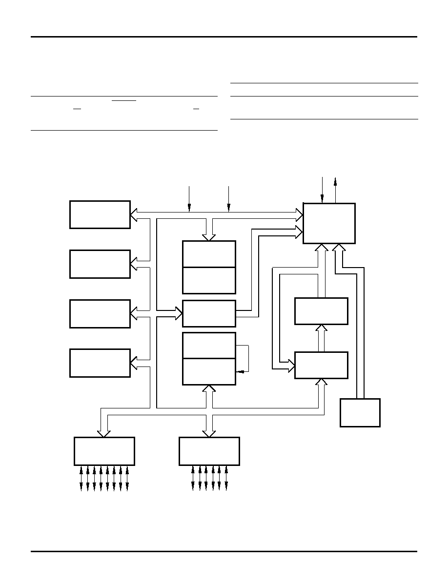
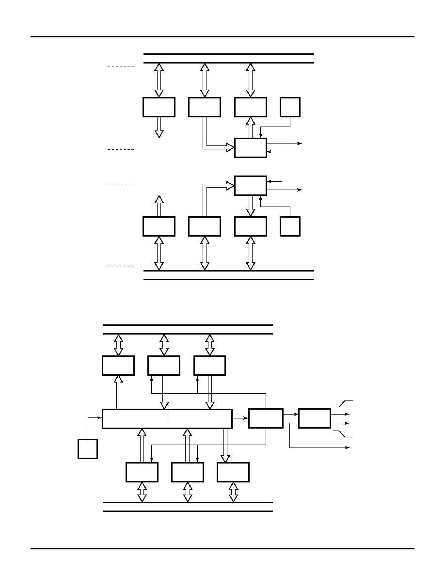
Figure 1. Functional Block Diagram
Two 8-Bit Timers
or One 16-Bit
PWM Timer
One 16-Bit
Standard Timer
Interrupt
Control
One Analog
Comparator
Port A
I/O
ALU
FLAGS
WDT
Register
Pointer
RAM
Register File
Machine
Timing
OTP Program
Memory
Program
Counter
GND
XTAL
Port B
POR &
I/O
V
CC
BO
V
Z8PE002
ZiLOG
Z8Plus OTP Microcontroller
DS008700-Z8X0799
P R E L I M I N A R Y
3
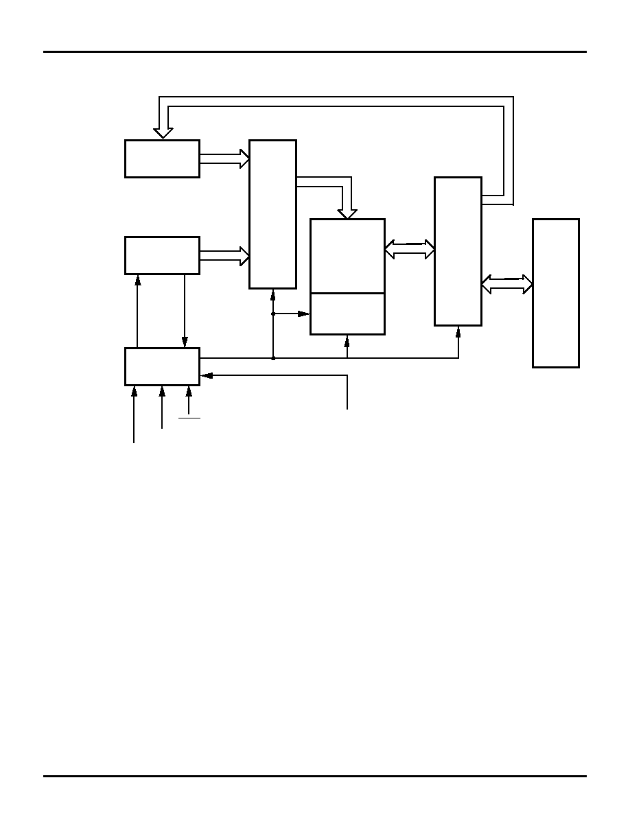
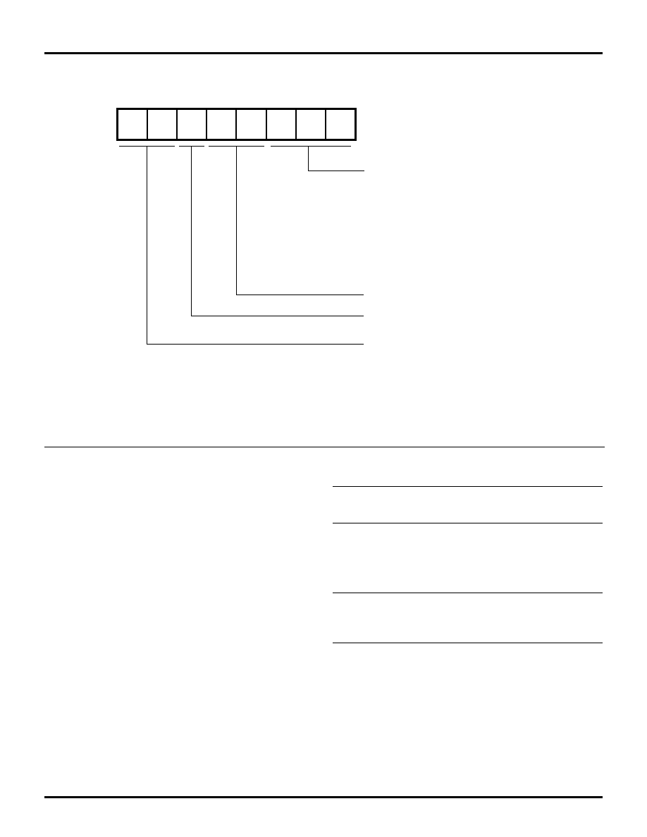
Figure 2. EPROM Programming Mode Block Diagram
Address
MUX
EPROM
Option
Bits
AD 9≠0
AD 9≠0
AD 9≠0
D7≠0
D7≠0
Z8Plus Core
Address
Counter
PGM + Test
Mode Logic
XTAL
ADCLK
PGM
Data
MUX
Port
A
ADCLR/V
PP
Z8PE002
Z8Plus OTP Microcontroller
ZiLOG
4
P R E L I M I N A R Y
DS008700-Z8X0799
PIN DESCRIPTION
Figure 3. 18-Pin DIP/SOIC Pin Identification
Table 1. Standard Programming Mode
Pin #
Symbol
Function
Direction
1≠5
PB1≠PB5
Port B, Pins 1,2,3,4,5
Input/Output
6≠9
PA7≠PA4
Port A, Pins 7,6,5,4
Input/Output
10≠13
PA3≠PA0
Port A, Pins 3,2,1,0
Input/Output
14
V
CC
Power Supply
15
V
SS
Ground
16
XTAL2
Crystal Oscillator Clock
Output
17
XTAL1
Crystal Oscillator Clock
Input
18
PB0
Port B, Pin 0
Input/Output
PB1
PB2
PB3
PB4
PB5
PA7
PA6
PA5
PA4
PB0
XTAL1
XTAL2
V
SS
V
CC
PA0
PA1
PA2
PA3
18
18-Pin
DIP/SOIC
1
9
10

Z8PE002
ZiLOG
Z8Plus OTP Microcontroller
DS008700-Z8X0799
P R E L I M I N A R Y
5
Figure 4. 18-Pin DIP/SOIC Pin Identification
Table 2. EPROM Programming Mode
Pin #
Symbol
Function
Direction
1
PGM
Program Mode
Input
2≠4
GND
Ground
5
ADCLR/V
PP
Clear Clock/Program Voltage
Input
6≠9
D7≠D4
Data 7,6,5,4
Input/Output
10≠13
D3≠D0
Data 3,2,1,0
Input/Output
14
V
DD
Power Supply
15
GND
Ground
16
NC
No Connection
17
XTAL1
1-MHz Clock
Input
18
ADCLK
Address Clock
Input
PGM
GND
GND
GND
ADCLR/V
PP
D7
D6
D5
D4
ADCLK
XTAL1
NC
GND
V
DD
D0
D1
D2
D3
18
18-Pin
DIP/SOIC
1
9
10
Z8PE002
Z8Plus OTP Microcontroller
ZiLOG
6
P R E L I M I N A R Y
DS008700-Z8X0799
PIN DESCRIPTION
(Continued)
Figure 5. 20-Pin SSOP Pin Identification
Table 3. Standard Programming Mode
Pin #
Symbol
Function
Direction
1≠5
PB1≠PB5
Port B, Pins 1,2,3,4,5
Input/Output
6
NC
No Connection
7≠10
PA7≠PA4
Port A, Pins 7,6,5,4
Input/Output
11≠14
PA3≠PA0
Port A, Pins 3,2,1,0
Input/Output
15
NC
No Connection
16
V
CC
Power Supply
17
V
SS
Ground
18
XTAL2
Crystal Oscillator Clock
Output
19
XTAL1
Crystal Oscillator Clock
Input
20
PB0
Port B, Pin 0
Input/Output
PB1
PB2
PB3
PB4
PB5
NC
PA7
PA6
PA5
PA4
PB0
XTAL1
XTAL2
V
SS
V
CC
NC
PA0
PA1
PA2
PA3
20
20-Pin
SSOP
1
10
11

Z8PE002
ZiLOG
Z8Plus OTP Microcontroller
DS008700-Z8X0799
P R E L I M I N A R Y
7
Figure 6. 20-Pin SSOP Pin Identification/EPROM Programming Mode
Table 4. EPROM Programming Mode
Pin #
Symbol
Function
Direction
1
PGM
Program Mode
Input
2≠4
GND
Ground
5
ADCLR/V
PP
Clear Clock/Program Voltage
Input
6
NC
No Connection
7≠10
D7≠D4
Data 7,6,5,4
Input/Output
11≠14
D3≠D0
Data 3,2,1,0
Input/Output
15
NC
No Connection
16
V
DD
Power Supply
17
GND
Ground
18
NC
No Connection
19
XTAL1
1-MHz Clock
Input
20
ADCLK
Address Clock
Input
PGM
GND
GND
GND
ADCLR/V
PP
NC
D7
D6
D5
D4
ADCLK
XTAL1
NC
GND
V
DD
NC
D0
D1
D2
D3
20
20-Pin
SSOP
1
10
11

Z8PE002
Z8Plus OTP Microcontroller
ZiLOG
8
P R E L I M I N A R Y
DS008700-Z8X0799
ABSOLUTE MAXIMUM RATINGS
Stresses greater than those listed under Absolute Maximum
Ratings can cause permanent damage to the device. This rat-
ing is a stress rating only. Functional operation of the device
at any condition above those indicated in the operational
sections of these specifications is not implied. Exposure to
absolute maximum rating conditions for an extended period
can affect device reliability. Total power dissipation should
not exceed 880 mW for the package. Power dissipation is
calculated as follows:
Parameter
Min
Max
Units
Note
Ambient Temperature under Bias
≠40
+105
C
Storage Temperature
≠65
+150
C
Voltage on any Pin with Respect to V
SS
≠0.6
+7
V
1
Voltage on V
DD
Pin with Respect to V
SS
≠0.3
+7
V
Voltage on PB5 Pin with Respect to V
SS
≠0.6
V
DD
+1
V
2
Total Power Dissipation
880
mW
Maximum Allowable Current out of V
SS
40
mA
3
Maximum Allowable Current into V
DD
40
mA
3
Maximum Allowable Current into an Input Pin
≠600
+600
µA
4
Maximum Allowable Current into an Open-Drain Pin
≠600
+600
µA
5
Maximum Allowable Output Current Sunk by Any I/O Pin
25
mA
Maximum Allowable Output Current Sourced by Any I/O Pin
25
mA
Maximum Allowable Output Current Sunk by Port A
40
mA
3
Maximum Allowable Output Current Sourced by Port A
40
mA
3
Maximum Allowable Output Current Sunk by Port B
40
mA
3
Maximum Allowable Output Current Sourced by Port B
40
mA
3
Notes:
1. Applies to all pins except the PB5 pin and where otherwise noted.
2. There is no input protection diode from pin to V
DD
.
3. Peak Current. Do not exceed 25mA average current in either direction.
4. Excludes XTAL pins.
5. Device pin is not at an output Low state.
Total Power Dissipation = V
DD
x [I
DD
≠ (sum of I
OH
)]
+ sum of [(V
DD
≠ V
OH
) x I
OH
]
+ sum of (V
OL
x I
OL
)
Z8PE002
ZiLOG
Z8Plus OTP Microcontroller
DS008700-Z8X0799
P R E L I M I N A R Y
9
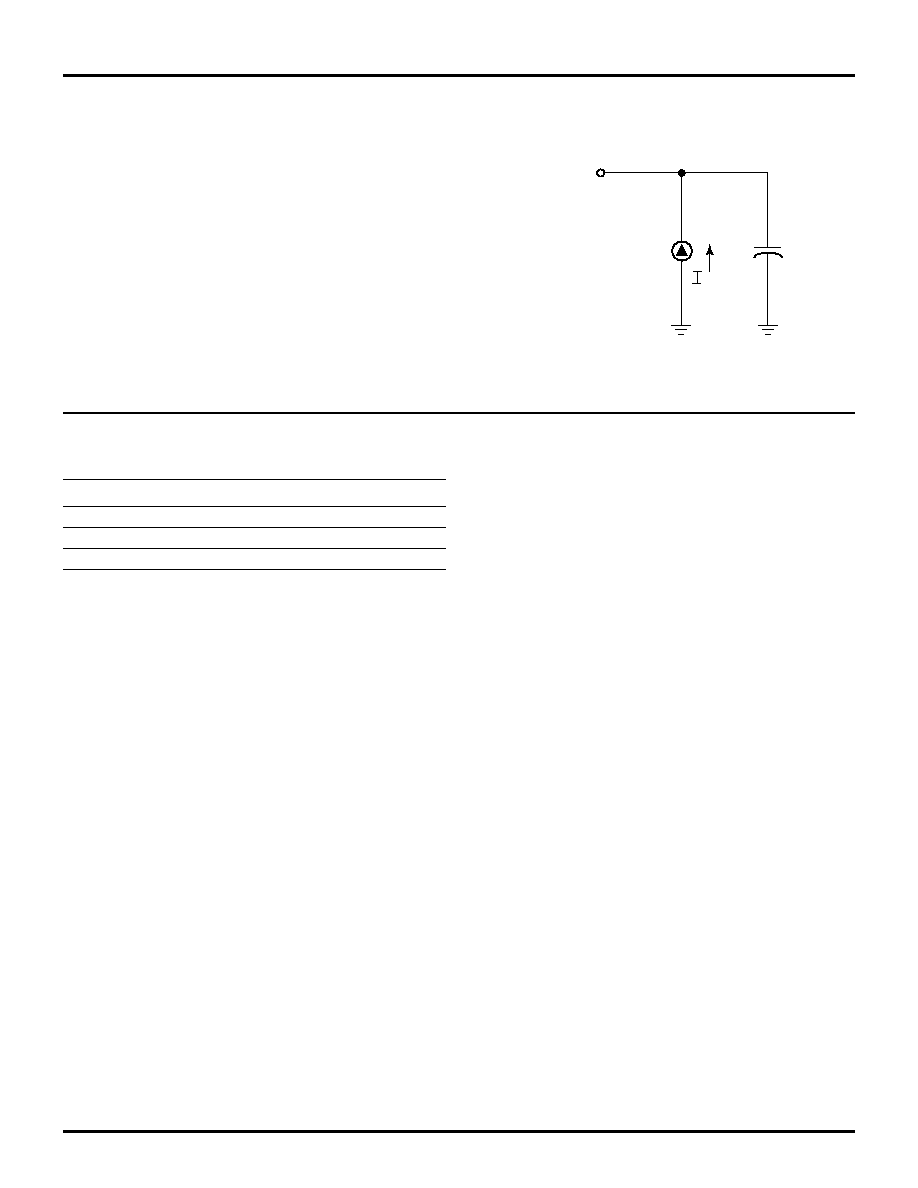
STANDARD TEST CONDITIONS
The characteristics listed below apply for standard test con-
ditions as noted. All voltages are referenced to Ground. Pos-
itive current flows into the referenced pin (Figure 7).
CAPACITANCE
T
A
= 25∫C, V
CC
= GND = 0V, f = 1.0 MHz, unmeasured pins returned to GND.
Figure 7. Test Load Diagram
From Output
Under Test
150 pF
Parameter
Min
Max
Input capacitance
0
12 pF
Output capacitance
0
12 pF
I/O capacitance
0
12 pF

Z8PE002
Z8Plus OTP Microcontroller
ZiLOG
10
P R E L I M I N A R Y
DS008700-Z8X0799
DC ELECTRICAL CHARACTERISTICS
Table 5. DC Electrical Characteristics
T
A
= 0∫C to +70∫C
Standard Temperatures
Typical
2
@ 25∞C
Sym
Parameter
V
CC
1
Min
Max
Units Conditions
Notes
V
CH
Clock Input High
Voltage
3.0V
0.7V
CC
V
CC
+0.3
1.3
V
Driven by External Clock
Generator
5.5V
0.7V
CC
V
CC
+0.3
2.5
V
Driven by External Clock
Generator
V
CL
Clock Input Low
Voltage
3.0V
V
SS
≠0.3
0.2V
CC
0.7
V
Driven by External Clock
Generator
5.5V
V
SS
≠0.3
0.2V
CC
1.5
V
Driven by External Clock
Generator
V
IH
Input High Voltage
3.0V
0.7V
CC
V
CC
+0.3
1.3 V
5.5V
0.7V
CC
V
CC
+0.3
2.5
V
V
IL
Input Low Voltage
3.0V
V
SS
≠0.3
0.2V
CC
0.7
V
5.5V
V
SS
≠0.3
0.2V
CC
1.5
V
V
OH
Output High Voltage
3.0V
V
CC
≠0.4
3.1
V
I
OH
= ≠2.0 mA
5.5V
V
CC
≠0.4
4.8
V
I
OH
= ≠2.0 mA
V
OL1
Output Low Voltage
3.0V
0.6
0.2
V
I
OL
= +4.0 mA
5.5V
0.4
0.1
V
I
OL
= +4.0 mA
V
OL2
Output Low Voltage
3.0V
1.2
0.5
V
I
OL
= +6 mA
5.5V
1.2
0.5
V
I
OL
= +12 mA
V
OFFSET
Comparator Input
Offset Voltage
3.0V
25.0
10.0
mV
5.5V
25.0
10.0
mV
I
IL
Input Leakage
3.0V
≠1.0
2.0
0.064
µA
V
IN
= 0V, V
CC
5.5V
≠1.0
2.0
0.064
µA
V
IN
= 0V, V
CC
I
OL
Output Leakage
3.0V
≠1.0
2.0
0.114
µA
V
IN
= 0V, V
CC
5.5V
≠1.0
2.0
0.114
µA
V
IN
= 0V, V
CC
V
ICR
Comparator Input
Common Mode
Voltage Range
3.0V
V
SS
≠0.3
V
CC
≠1.0
V
3
5.5V
V
SS
≠0.3
V
CC
≠1.0
V
3
R
PB5
PB5 Pull-up Resistor
3.0V
100
200
kOhm
4
5.5V
100
200
V
LV
V
CC
Low-Voltage
Protection
2.45
2.85
2.60
V
Notes:
1. The V
CC
voltage specification of 3.0V guarantees 3.0V; the V
CC
voltage specification of 5.5V guarantees 5.0V ±0.5V.
2. Typical values are measured at V
CC
= 3.3V and V
CC
= 5.0V; V
SS
= 0V = GND.
3. For the analog comparator input when the analog comparator is enabled.
4. No protection diode is provided from the pin to V
CC
. External protection is recommended.
5. All outputs are unloaded and all inputs are at the V
CC
or V
SS
level.
6. CL1 = CL2 = 22 pF.
7. Same as note 5, except inputs are at V
CC
.

Z8PE002
ZiLOG
Z8Plus OTP Microcontroller
DS008700-Z8X0799
P R E L I M I N A R Y
11
I
CC
Supply Current
3.0V
2.5
2.0
mA
@ 10 MHz
5,6
5.5V
6.0
3.5
mA
@ 10 MHz
5,6
I
CC1
Standby Current
3.0V
2.0
1.0
mA
HALT mode V
IN
= 0V,
V
CC
@ 10 MHz
5,6
5.5V
4.0
2.5
mA
HALT mode V
IN
= 0V,
V
CC
@ 10 MHz
5,6
I
CC2
Standby Current
500
150
nA
STOP mode V
IN
= 0V,
V
CC
7
Table 5. DC Electrical Characteristics (Continued)
T
A
= 0∫C to +70∫C
Standard Temperatures
Typical
2
@ 25∞C
Sym
Parameter
V
CC
1
Min
Max
Units Conditions
Notes
Notes:
1. The V
CC
voltage specification of 3.0V guarantees 3.0V; the V
CC
voltage specification of 5.5V guarantees 5.0V ±0.5V.
2. Typical values are measured at V
CC
= 3.3V and V
CC
= 5.0V; V
SS
= 0V = GND.
3. For the analog comparator input when the analog comparator is enabled.
4. No protection diode is provided from the pin to V
CC
. External protection is recommended.
5. All outputs are unloaded and all inputs are at the V
CC
or V
SS
level.
6. CL1 = CL2 = 22 pF.
7. Same as note 5, except inputs are at V
CC
.

Z8PE002
Z8Plus OTP Microcontroller
ZiLOG
12
P R E L I M I N A R Y
DS008700-Z8X0799
DC ELECTRICAL CHARACTERISTICS (Continued)
Table 6. DC Electrical Characteristics
T
A
= ≠40∫C to +105∫C
Extended Temperatures
Typical
2
@ 25∞C
Sym
Parameter
V
CC
1
Min
Max
Units Conditions
Notes
V
CH
Clock Input High
Voltage
4.5V
0.7 V
CC
V
CC
+0.3
2.5
V
Driven by External
Clock Generator
5.5V
0.7 V
CC
V
CC
+0.3
2.5
V
Driven by External
Clock Generator
V
CL
Clock Input Low
Voltage
4.5V
V
SS
≠0.3
0.2 V
CC
1.5
V
Driven by External
Clock Generator
5.5V
V
SS
≠0.3
0.2 V
CC
1.5
V
Driven by External
Clock Generator
V
IH
Input High Voltage
4.5V
0.7 V
CC
V
CC
+0.3
2.5
V
5.5V
0.7 V
CC
V
CC
+0.3
2.5
V
V
IL
Input Low Voltage
4.5V
V
SS
≠0.3
0.2 V
CC
1.5
V
5.5V
V
SS
≠0.3
0.2 V
CC
1.5
V
V
OH
Output High
Voltage
4.5V
V
CC
≠0.4
4.8
V
I
OH
= ≠2.0 mA
5.5V
V
CC
≠0.4
4.8
V
I
OH
= ≠2.0 mA
V
OL1
Output Low
Voltage
4.5V
0.4
0.1
V
I
OL
= +4.0 mA
5.5V
0.4
0.1
V
I
OL
= +4.0 mA
V
OL2
Output Low
Voltage
4.5V
1.2
0.5
V
I
OL
= +12 mA
5.5V
1.2
0.5
V
I
OL
= +12 mA
V
OFFSET
Comparator Input
Offset Voltage
4.5V
25.0
10.0
mV
5.5V
25.0
10.0
mV
I
IL
Input Leakage
4.5V
≠1.0
2.0
<1.0
µA
V
IN
= 0V, V
CC
5.5V
≠1.0
2.0
<1.0
µA
V
IN
= 0V, V
CC
I
OL
Output Leakage
4.5V
≠1.0
2.0
<1.0
µA
V
IN
= 0V, V
CC
5.5V
≠1.0
2.0
<1.0
µA
V
IN
= 0V, V
CC
V
ICR
Comparator Input
Common Mode
Voltage Range
4.5V
0 V
CC
≠1.5V
V
3
5.5V
0
V
CC
≠1.5V
V
3
R
PB5
PB5 Pull-up
Resistor
4.5V
100
200
kOhm
4
5.5V
100
200
V
LV
V
CC
Low-Voltage
Protection
2.45
2.85
2.60
V
I
CC
Supply Current
4.5V
7.0
4.0
mA
@ 10 MHz
5,6
5.5V
7.0
4.0
mA
@ 10 MHz
5,6
Notes:
1. The V
CC
voltage specification of 4.5V and 5.5V guarantees 5.0V ±0.5V.
2. Typical values are measured at V
CC
= 5.0V; V
SS
= 0V = GND.
3. For analog comparator input when analog comparator is enabled.
4. No protection diode is provided from the pin to V
CC
. External protection is recommended.
5. All outputs are unloaded and all inputs are at V
CC
or V
SS
level.
6. CL1 = CL2 = 22 pF.
7. Same as note 5, except inputs are at V
CC
.

Z8PE002
ZiLOG
Z8Plus OTP Microcontroller
DS008700-Z8X0799
P R E L I M I N A R Y
13
I
CC1
Standby Current
4.5V
2.0
1.0
mA
HALT mode V
IN
= 0V,
V
CC
@ 10 MHz
5,6
5.5V
2.0
1.0
mA
HALT mode V
IN
= 0V,
V
CC
@ 10 MHz
5,6
I
CC2
Standby Current
4.5V
700
250
nA
STOP mode V
IN
= 0V,V
CC
7
5.5V
700
250
nA
STOP mode V
IN
= 0V,V
CC
7
Table 6. DC Electrical Characteristics (Continued)
T
A
= ≠40∫C to +105∫C
Extended Temperatures
Typical
2
@ 25∞C
Sym
Parameter
V
CC
1
Min
Max
Units Conditions
Notes
Notes:
1. The V
CC
voltage specification of 4.5V and 5.5V guarantees 5.0V ±0.5V.
2. Typical values are measured at V
CC
= 5.0V; V
SS
= 0V = GND.
3. For analog comparator input when analog comparator is enabled.
4. No protection diode is provided from the pin to V
CC
. External protection is recommended.
5. All outputs are unloaded and all inputs are at V
CC
or V
SS
level.
6. CL1 = CL2 = 22 pF.
7. Same as note 5, except inputs are at V
CC
.
Z8PE002
Z8Plus OTP Microcontroller
ZiLOG
14
P R E L I M I N A R Y
DS008700-Z8X0799
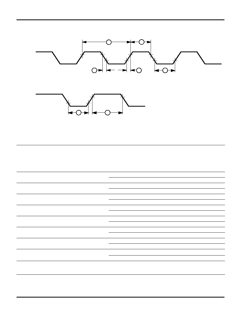
AC ELECTRICAL CHARACTERISTICS
Figure 8. AC Electrical Timing Diagram
Table 7. Additional Timing
T
A
= 0∫C to +70∫C
T
A
= ≠40∫C to +105∫C
@ 10 MHz
No
Symbol
Parameter
V
CC
1
Min
Max
Units
Notes
1
T
P
C
Input Clock Period
3.0V
100
DC
ns
2
5.5V
100
DC
ns
2
2
T
R
C,T
F
C
Clock Input Rise and Fall Times
3.0V
15
ns
2
5.5V
15
ns
2
3
T
W
C
Input Clock Width
3.0V
50
ns
2
5.5V
50
ns
2
4
T
W
IL
Int. Request Input Low Time
3.0V
70
ns
2
5.5V
70
ns
2
5
T
W
IH
Int. Request Input High Time
3.0V
5TpC
2
5.5V
5TpC
2
6
T
WSM
STOP mode Recovery Width
Spec.
3.0V
25
ns
5.5V
25
ns
7
T
OST
Oscillator Start-Up Time
3.0V
5TpC
5.5V
5TpC
8
T
POR
Power-On Reset Time
3.0V
128 T
P
C + T
OST
5.5V
Notes:
1. The V
DD
voltage specification of 3.0V guarantees 3.0V. The V
DD
voltage specification of 5.5V guarantees 5.0V
±
0.5V.
2. Timing Reference uses 0.7 V
CC
for a logical 1 and 0.2 V
CC
for a logical 0.
1
3
4
2
2
3
5
Clock
IRQ
N

Z8PE002
ZiLOG
Z8Plus OTP Microcontroller
DS008700-Z8X0799
P R E L I M I N A R Y
15
Z8PLUS CORE
The device is based on the ZiLOG Z8Plus Core Architec-
ture. This core is capable of addressing up to 32 KB of pro-
gram memory and 4 KB of RAM. Register RAM is accessed
as either 8- or 16-bit registers using a combination of 4-,
8-, and 12-bit addressing modes. The architecture supports
up to 15 vectored interrupts from external and internal
sources. The processor decodes 44 CISC instructions using
6 addressing modes. See the
Z8Plus User's Manual
for more
information.
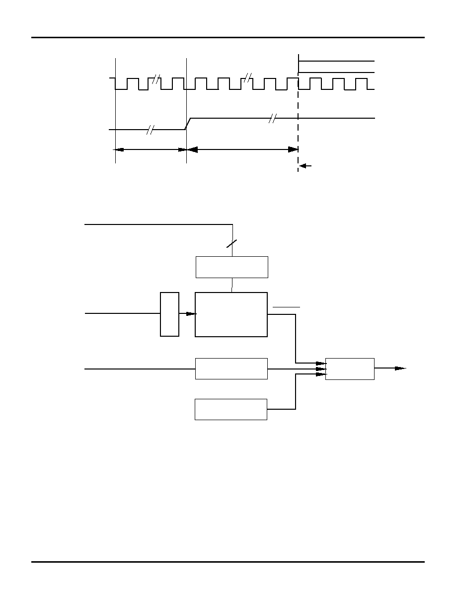
RESET
This section describes the Z8Plus reset conditions, reset
timing, and register initialization procedures. Reset is gen-
erated by the Voltage Brown-Out/Power-On Reset
(
VBO/POR
), Watch-Dog Timer (
WDT
), and Stop-Mode
Recovery (
SMR
).
A system reset overrides all other operating conditions and
puts the Z8Plus device into a known state. To initialize the
chip's internal logic, the
POR
device counts 64 internal
clock cycles after the oscillator stabilizes. The control reg-
isters and ports are not reset to their default conditions after
wakeup from a
STOP
mode or
WDT
time-out.
During
RESET
, the value of the program counter is
0020H
.
The I/O ports and control registers are configured to their
default reset state. Resetting the device does not affect the
contents of the general-purpose registers.
The
RESET
circuit initializes the control and peripheral reg-
isters, as shown in Table 8. Specific reset values are indi-
cated by a
1
or a
0
, while bits whose states are unchanged
or unknown from Power-Up are indicated by the letter
U
.
Program execution starts 10 External Crystal (
XTAL
) clock
cycles after the
POR
delay. The initial instruction fetch is
from location
0020H
. Figure 9 indicates reset timing.
After a reset, the first routine executed must be one that ini-
tializes the
TCTLHI
control register to the required system
configuration This activity is followed by initialization of
the remaining control registers.
Table 8. Control and Peripheral Registers*
Register (HEX)
Register Name
Bits
Comments
7
6
5
4
3
2
1
0
FF
Stack Pointer
0
0
U
U
U
U
U
U Stack pointer is not affected by RESET.
FE
Reserved
FD
Register Pointer
U
U
U
U
0
0
0
0
Register pointer is not affected by
RESET.
FC
Flags
U
U
U
U
U
U
*
*
Only WDT & SMR flags are affected by
RESET.
FB
Interrupt Mask
0
0
0
0
0
0
0
0
All interrupts masked by RESET.
FA
Interrupt
Request
0
0
0
0
0
0
0
0
All interrupt requests cleared by
RESET.
F9≠F0
Reserved
EF≠E0
Virtual Copy
Virtual copy of the current working
register set.
DF≠D8
Reserved
D7
Port B Special
Function
0
0
0
0
0
0
0
0
Deactivates all port special functions
after RESET.
D6
Port B
Directional
Control
0
0
0
0
0
0
0
0
Defines all bits as inputs in PortB after
RESET.
D5
Port B Output
U
U
U
U
U
U
U
U Output register not affected by RESET.
Note:
*The SMR and WDT flags are set to indicate the source of the RESET.

Z8PE002
Z8Plus OTP Microcontroller
ZiLOG
16
P R E L I M I N A R Y
DS008700-Z8X0799
RESET (Continued)
D4
Port B Input
U
U
U
U
U
U
U
U Current sample of the input pin
following RESET.
D3
Port A Special
Function
0
0
0
0
0
0
0
0
Deactivates all port special functions
after RESET.
D2
Port A
Directional
Control
0
0
0
0
0
0
0
0
Defines all bits as inputs in PortA after
RESET.
D1
Port A Output
U
U
U
U
U
U
U
U Output register not affected by RESET
D0
Port A Input
U
U
U
U
U
U
U
U Current sample of the input pin
following RESET.
CF
Reserved
CE
Reserved
CD
T1VAL
U
U
U
U
U
U
U
U
CC
T0VAL
U
U
U
U
U
U
U
U
CB
T3VAL
U
U
U
U
U
U
U
U
CA
T2VAL
U
U
U
U
U
U
U
U
C9
T3AR
U
U
U
U
U
U
U
U
C8
T2AR
U
U
U
U
U
U
U
U
C7
T1ARHI
U
U
U
U
U
U
U
U
C6
T0ARHI
U
U
U
U
U
U
U
U
C5
T1ARLO
U
U
U
U
U
U
U
U
C4
T0ARLO
U
U
U
U
U
U
U
U
C3
WDTHI
1
1
1
1
1
1
1
1
C2
WDTLO
1
1
1
1
1
1
1
1
C1
TCTLHI
1
1
1
1
1
0
0
0
WDT enabled in HALT mode, WDT
time-out at maximum value, STOP
mode disabled.
C0
TCTLLO
0
0
0
0
0
0
0
0
All standard timers are disabled.
Table 8. Control and Peripheral Registers* (Continued)
Register (HEX)
Register Name
Bits
Comments
7
6
5
4
3
2
1
0
Note:
*The SMR and WDT flags are set to indicate the source of the RESET.
Table 9. Flag Register Bit D1, D0
D1
D0
Reset Source
0
0
V
BO
/POR
0
1
SMR Recovery
1
0
WDT Reset
1
1
Reserved
Z8PE002
ZiLOG
Z8Plus OTP Microcontroller
DS008700-Z8X0799
P R E L I M I N A R Y
17
Figure 9. Reset Timing
Figure 10. Reset Circuitry with POR, WDT, V
BO
, and SMR
First Machine Cycle
Clock
Internal
First Instruction Fetch
128 XTAL Clock Cycles
10 XTAL CLOCK CYCLES
Reset
XTAL
˜64
TCTLHI
D6,D5,D4
3
64 SCLK
SMR
(PB0)
WDTRST
16-Bit Timer
WDT Tap Select
Watch-Dog Timer
SMR Logic
V
BO
/POR
POR Delay

Z8PE002
Z8Plus OTP Microcontroller
ZiLOG
18
P R E L I M I N A R Y
DS008700-Z8X0799
INTERRUPT SOURCES
Table 10 presents the interrupt types, sources, and vectors
available in the Z8Plus. Other processors from the Z8Plus
family may define the interrupts differently.
External Interrupt Sources
External sources can be generated by a transition on the cor-
responding port pin. The interrupt may detect a rising edge,
a falling edge, or both.
Notes: The interrupt sources and trigger conditions are device
dependent. See the device product specification to de-
termine available sources (internal and external), trig-
gering edge options, and exact programming details.
Although interrupts are edge triggered, minimum inter-
rupt request Low and High times must be observed for
proper operation. See the device product specification
for exact timing requirements on external interrupt re-
quests (
T
W
IL
,
T
W
IH
).
Internal Interrupt Sources
Internal interrupt sources and trigger conditions are device
dependent. On-chip peripherals may set interrupt under var-
ious conditions. Some peripherals always set their corre-
sponding
IREQ
bit while others must be specifically con-
figured to do so.
See the device product specification to determine available
sources, triggering edge options, and exact programming
details. For more details on the interrupt sources, refer to
the chapters describing the timers, comparators, I/O ports,
and other peripherals.
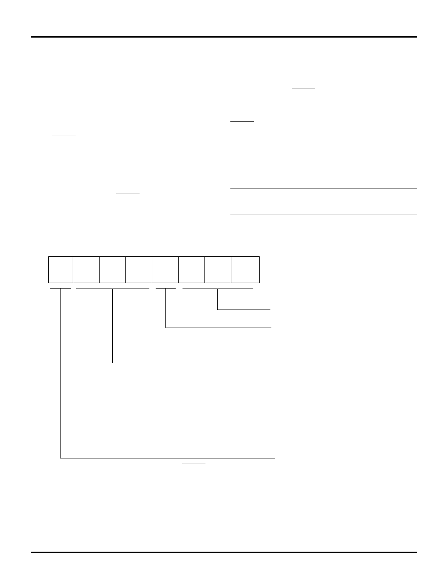
Interrupt Mask Register (IMASK) Initialization
The
IMASK
register individually or globally enables or dis-
ables the interrupts (Table 11). When bits
0
through
5
are
set to
1
, the corresponding interrupt requests are enabled.
Bit
7
is the master enable bit and must be set before any of
the individual interrupt requests can be recognized. Reset-
ting bit
7
disables all the interrupt requests. Bit
7
is set and
reset by the
EI
and
DI
instructions. It is automatically set to
0
during an interrupt service routine and set to
1
following
the execution of an Interrupt Return (
IRET
) instruction. The
IMASK
registers are
reset
to
00h
, disabling all interrupts.
Notes: It is not good programming practice to directly assign a
value to the master enable bit. A value change should
always be accomplished by issuing the
EI
and
DI
in-
structions.
Care should be taken not to set or clear
IMASK
bits
while the master enable is set.
Table 10. Interrupt Types, Sources, and Vectors
Name
Sources
Vector Location
Comments
Fixed Priority
IREQ
0
Timer0 Time-out
2,3
Internal
1 (Highest)
IREQ
1
PB4 High-to-Low
Transition
4,5
External (PB4), Edge
Triggered
2
IREQ
2
Timer1 Time-out
6,7
Internal
3
IREQ
3
PB2 High-to-Low
Transition
8,9
External (PB2), Edge
Triggered
4
IREQ
4
PB4 Low-to-High
Transition
A,B
External (PB4), Edge
Triggered
5
IREQ
5
Timer2 Time-out
C,D
Internal
6 (Lowest)
IREQ
6
≠IREQ
15
Reserved
Reserved for future
expansion

Z8PE002
ZiLOG
Z8Plus OTP Microcontroller
DS008700-Z8X0799
P R E L I M I N A R Y
19
Interrupt Request (IREQ) Register Initialization
IREQ
(Table 12) is a register that stores the interrupt re-
quests for both vectored and polled interrupts. When an in-
terrupt is issued, the corresponding bit position in the reg-
ister is set to
1
. Bits
0
to
5
are assigned to interrupt requests
IREQ0
to
IREQ5
, respectively.
Whenever
RESET
is executed, the
IREQ
resistor is set to
00h
.
Table 11. Interrupt Mask Register--IMASK (FBh)
Bit
7
6
5
4
3
2
1
0
R/W
R/W R/W R/W R/W
R/W R/W R/W R/W
Reset
0
0
0
0
0
0
0
0
R = Read W = Write X = Indeterminate U = Undefined/
Undetermined
Bit
Position
R/W
Value
Description
7
0
1
Disables Interrupts
Enables Interrupts
6
0
Reserved, must be 0
5
0
1
Disables IRQ5
Enables IRQ5
4
0
1
Disables IRQ4
Enables IRQ4
3
0
1
Disables IRQ3
Enables IRQ3
2
0
1
Disables IRQ2
Enables IRQ2
1
0
1
Disables IRQ1
Enables IRQ1
0
0
1
Disables IRQ0
Enables IRQ0
Table 12. Interrupt Request Register≠IREQ (FAh)
Bit
7
6
5
4
3
2
1
0
R/W
R/W R/W R/W R/W
R/W R/W R/W R/W
Reset
0
0
0
0
0
0
0
0
R = Read W = Write X = Indeterminate U = Undefined/
Undetermined
Bit
Position
R/W
Value
Description
7
R/W
0
Reserved, must be 0
6
R/W
0
Reserved, must be 0
5
R/W
0
1
IRQ5 reset
IRQ5 set
4
R/W
0
1
IRQ4 reset
IRQ4 set
3
R/W
0
1
IRQ3 reset
IRQ3 set
2
R/W
0
1
IRQ2 reset
IRQ2 set
1
R/W
0
1
IRQ1 reset
IRQ1 set
0
R/W
0
1
IRQ0 reset
IRQ0 set

Z8PE002
Z8Plus OTP Microcontroller
ZiLOG
20
P R E L I M I N A R Y
DS008700-Z8X0799
IREQ SOFTWARE INTERRUPT GENERATION
IREQ
can be used to generate software interrupts by spec-
ifying
IREQ
as the destination of any instruction referencing
the Z8Plus Standard Register File. These software inter-
rupts (
SWI
) are controlled in the same manner as hardware
generated requests. In other words, the
IMASK
controls the
enabling of each
SWI
.
To generate a
SWI
, the request bit in
IREQ
is set by the fol-
lowing statement:
OR IREQ,#NUMBER
The immediate data variable,
NUMBER
, has a
1
in the bit
position corresponding to the required level of
SWI
. For ex-
ample, an
SWI
must be issued when an
IREQ5
occurs. Bit
5
of
NUMBER
must have a value of
1
.
OR IREQ, #00100000B
If the interrupt system is globally enabled,
IREQ5
is en-
abled, and there are no higher priority requests pending,
control is transferred to the service routine pointed to by the
IREQ5
vector.
Note: Software may modify the
IREQ
register at any time. Care
should be taken when using any instruction that modifies
the
IREQ
register while interrupt sources are active. The
software writeback always takes precedence over the
hardware. If a software writeback takes place on the
same cycle as an interrupt source tries to set an
IREQ
bit,
the new interrupt is lost.
Nesting of Vectored Interrupts
Nesting vectored interrupts allows higher priority requests
to interrupt a lower priority request. To initiate vectored in-
terrupt nesting, perform the following steps during the in-
terrupt service routine:
∑
PUSH
the old
IMASK
on the stack
∑
Load
IMASK
with a new mask to disable lower prior-
ity interrupts
∑
Execute an
EI
instruction
∑
Proceed with interrupt processing
∑
Execute a
DI
instruction after processing is complete
∑
Restore the
IMASK
to its original value by
POP
ing the
previous mask from the stack
∑
Execute
IRET
Depending on the application, some simplification of the
above procedure may be possible.
RESET Conditions
The
IMASK
and
IREQ
registers initialize to
00h
on
RESET
.
PROGRAMMABLE OPTIONS
EPROM Protect.
When selecting the
DISABLE EPROM
PROTECT/ENABLE TESTMODE
option, the user can read
the software code in the program memory. ZiLOG's inter-
nal factory test mode, or any of the standard test mode meth-
ods, are useful for reading or verifying the code in the mi-
crocontroller when using an EPROM programmer. If the
user should select the
ENABLE EPROM PROTECT/DIS-
ABLE TESTMODE
option, it is not possible to read the code
using a tester, programmer, or any other standard method.
As a result, ZiLOG is unable to test the EPROM memory
at any time after customer delivery.
This option bit only affects the user's ability to read the code
and has no effect on the operation of the part in an appli-
cation. ZiLOG tests the EPROM memory before customer
delivery whether or not the
ENABLE EPROM PRO-
TECT/DISABLE TESTMODE
option is selected; ZiLOG
provides a standard warranty for the part.
System Clock Source.
When selecting the
RC OSCILLA-
TOR ENABLE
option, the oscillator circuit on the micro-
controller is configured to work with an external RC circuit.
When selecting the Crystal/Other Clock Source option, the
oscillator circuit is configured to work with an external
crystal, ceramic resonator, or LC oscillator.
Z8PE002
ZiLOG
Z8Plus OTP Microcontroller
DS008700-Z8X0799
P R E L I M I N A R Y
21
WATCH-DOG TIMER
The Watch-Dog Timer (
WDT
) is a retriggerable one-shot
16-bit timer that resets the device
if it reaches its terminal
count. The
WDT
is driven by the
XTAL2
clock pin. To pro-
vide the longer time-out periods required in applications,
the watch-dog timer is only updated every 64th clock cycle.
When operating in the
RUN
or
HALT
modes, a
WDT
time-
out reset is functionally equivalent to an interrupt vectoring
the PC to
0020H
, and setting the
WDT
flag to
1
. Coming
out of
RESET
, the
WDT
is fully enabled with its time-out
value set at minimum, unless otherwise programmed during
the first instruction. Subsequent executions of the
WDT
in-
struction reinitialize the watch-dog timer registers (
C2h
and
C3h
) to their initial values as defined by bits
D6
,
D5
, and
D4
of the
TCTLHI
register. The
WDT
cannot be disabled ex-
cept on the first cycle after
RESET
and when the device en-
ters
STOP
mode.
The
WDT
instruction should be executed often enough to
provide some margin of time to allow the
WDT
registers to
approach
0
. Because the
WDT
time-out periods are rela-
tively long, a
WDT
RESET
occurs in the unlikely event that
the
WDT
times out on exactly the same cycle that the
WDT
instruction is executed.
RESET
clears both the
WDT
and
SMR
flags. A
WDT
time-
out sets the
WDT
flag, and the
STOP
instruction sets the
SMR
flag. This function enables software to determine
whether a
WDT
time-out or a return from
STOP
mode oc-
curred. Reading the
WDT
and
SMR
flags does not reset the
flag to
0
; therefore, the user must clear the flag via software.
Note: Failure to clear the
SMR
flag can result in unexpected
behavior.
Figure 11. TCTLHI Register for Control of WDT
D7
D6
D5
D4
D3
D2
D1
D0
0C1
TCTLHI
Reserved (must be 0)
0 = STOP mode enabled
1 = STOP mode disabled*
D6 D5 D4 WDT TIMEOUT VALUE
---- ---- ---- --------------------------------
0 0 0 Disabled
0 0 1 65,536 TpC*
0 1 0 131,072 TpC
0 1 1 262,144 TpC
1 0 0 524,288 TpC
1 0 1 1,048,576 TpC
1 1 0 2,097,152 TpC
1 1 1 8,388,608 TpC
(XTAL clocks to time-out)
1 = WDT enabled in HALT mode*
0 = WDT disabled in HALT mode
*Designates the default value after RESET.

Z8PE002
Z8Plus OTP Microcontroller
ZiLOG
22
P R E L I M I N A R Y
DS008700-Z8X0799
Note:
The
WDT
can only be disabled via software if the first in-
struction out of the
RESET
performs this function. Logic
within the device detects that it is in the process of exe-
cuting the first instruction after the processor leaves
RE-
SET
. During the execution of this instruction, the upper
five bits of the
TCTLHI
register can be written. After this
first instruction, hardware does not allow the upper five
bits of this register to be written.
The
TCTLHI
bits for control of the
WDT
are described be-
low:
WDT Time Select (D6, D5, D4).
Bits 6, 5, and 4 determine
the time-out period. Table 13 indicates the range of time-
out values that can be obtained. The default values of
D6
,
D5
, and
D4
are
001
, which sets the
WDT
to its minimum
time-out period when coming out of
RESET
.
WDT During HALT (D7).
This bit determines whether or
not the
WDT
is active during
HALT
mode. A
1
indicates ac-
tive during
HALT
mode. A
0
prevents the
WDT
from reset-
ting the part while halted. Coming out of
RESET
, the
WDT
is enabled during
HALT
mode.
STOP MODE (D3).
Coming out of
RESET
, the device
STOP
mode is disabled. If an application requires use of
STOP
mode, bit D3 must be cleared immediately at leaving
RESET
. If bit D3 is set, the
STOP
instruction executes as a
NOP
. If bit D3 is cleared, the
STOP
instruction enters
STOP
mode.
Bits 2, 1 and 0.
These bits are reserved and must be
0
.
POWER-DOWN MODES
In addition to the standard RUN mode, the Z8Plus MCU
supports two Power-Down modes to minimize device cur-
rent consumption. The two modes supported are
HALT
and
STOP
.
HALT MODE OPERATION
The
HALT
mode suspends instruction execution and turns
off the internal CPU clock. The on-chip oscillator circuit
remains active so the internal clock continues to run and is
applied to the timers and interrupt logic.
To enter
HALT
mode, the device only requires a
HALT
in-
struction. It is not necessary to execute a
NOP
instruction
immediately before the
HALT
instruction.
HALT
mode can be exited by servicing an external or inter-
nal interrupt. The first instruction executed is the interrupt
service routine. At completion of the interrupt service rou-
tine, the user program continues from the instruction after
the
HALT
instruction.
The
HALT
mode can also be exited via a
RESET
activation
or a Watch-Dog Timer (
WDT
) time-out. In these cases, pro-
gram execution restarts at
0020H
, the reset restart address.
Table 13. WDT Time-Out
D6
D5
D4
Crystal Clocks*
to Timeout
Time-Out Using
a 10-MHz Crystal
0
0
0
Disabled Disabled
0
0
1
65,536 TpC
6.55 ms
0
1
0
131,072 TpC
13.11 ms
0
1
1
262,144 TpC
26.21 ms
1
0
0
524,288 TpC
52.43 ms
1
0
1
1,048,576 TpC
104.86 ms
1
1
0
2,097,152 TpC
209.72 ms
1
1
1
8,388,608 TpC
838.86 ms
Note:
*TpC is an XTAL clock cycle. The default at reset is 001.
7F
HALT
; enter HALT mode

Z8PE002
ZiLOG
Z8Plus OTP Microcontroller
DS008700-Z8X0799
P R E L I M I N A R Y
23
STOP MODE OPERATION
The
STOP
mode provides the lowest possible device stand-
by current. This instruction turns off the on-chip oscillator
and internal system clock.
To enter the
STOP
mode, the Z8Plus only requires a
STOP
instruction. It is not necessary to execute a
NOP
instruction
immediately before the
STOP
instruction.
The
STOP
mode is exited by any one of the following resets:
POR
or a Stop-Mode Recovery source. At reset generation,
the processor always restarts the application program at ad-
dress
0020H
, and the
STOP
mode flag is set. Reading the
STOP
mode flag does not clear it. The user must clear the
STOP
mode flag with software.
Note: Failure to clear the
STOP
mode flag can result in unde-
fined behavior.
The Z8Plus provides a dedicated Stop-Mode Recovery
(
SMR
) circuit. In this case, a low-level applied to input pin
PB0
(I/O Port B, bit 0) triggers an
SMR
. To use this mode,
pin
PB0
must be configured as an input and the special func-
tion selected before the
STOP
mode is entered. The Low
level on
PB0
must be held for a minimum pulse width
T
WSM
. Program execution starts at address
20h
, after the
POR
delay.
Notes: 1. The
PB0
input, when used for Stop-Mode Recovery,
does not initialize the control registers.
The
STOP
mode current (
I
CC2
) is minimized when:
∑
V
CC
is at the low end of the device's operating range
∑
Output current sourcing is minimized
∑
All inputs (digital and analog) are at the Low or High
rail voltages
2. For detailed information about flag settings, see the
Z8Plus User's Manual
.
6F
STOP
;enter STOP mode
Z8PE002
Z8Plus OTP Microcontroller
ZiLOG
24
P R E L I M I N A R Y
DS008700-Z8X0799
CLOCK
The Z8Plus MCU derives its timing from on-board clock
circuitry connected to pins
XTAL1
and
XTAL2
. The clock
circuitry consists of an oscillator, a glitch filter, and a di-
vide-by-two shaping circuit. Figure 12 illustrates the clock
circuitry. The oscillator's input is
XTAL1
and its output is
XTAL2
. The clock can be driven by a crystal, a ceramic res-
onator, LC clock, or an external clock source.
By selecting the
RC OSCILLATOR
option in the graphical
user interface (GUI), the circuit may instead be driven by
an external Resistor and Capacitor (
RC
) oscillator. Figure
13 illustrates this configuration. This design is limited to no
more than 4 MHz to restrict EMI noise.
Note: The reduced drive strength of this configuration also al-
lows the clock circuit to use a micropower-type crystal
(also known as a tuning fork) without reduction resis-
tors.
Figure 12. Clock Circuit
˜2
XTAL2
XTAL1
Glitch
Filter
˜4
˜8
WDT
Clock
Timer
Clock (TCLK)
Machine
Clock (SCLK)
(5 cycles
per in-
struction)
Figure 13. Z8Plus in RC Oscillator Mode
Glitch
Filter
SS
XTAL2
XTAL1
Note:
4 MHz max.
˜
2
R
C
V Pin
Z8PE002
ZiLOG
Z8Plus OTP Microcontroller
DS008700-Z8X0799
P R E L I M I N A R Y
25
OSCILLATOR OPERATION
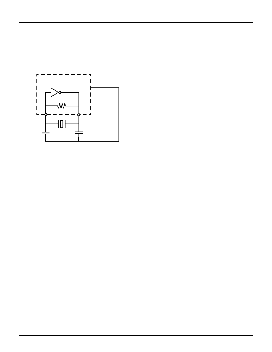
The Z8Plus MCU uses a Pierce oscillator with an internal
feedback resistor (Figure 14). The advantages of this circuit
are low-cost, large output signal, low-power level in the
crystal, stability with respect to
V
CC
and temperature, and
low impedances (not disturbed by stray effects).
One drawback to the Pierce oscillator is the requirement for
high gain in the amplifier to compensate for feedback path
losses. The oscillator amplifies its own noise at start-up until
it settles at the frequency that satisfies the gain/phase re-
quirements.
A x B = 1
; where
A = VO/VI
is the gain of the
amplifier, and
B = VI/VO
is the gain of the feedback element.
The total phase shift around the loop is forced to
0
(360 de-
grees).
V
IN
must be in phase with itself; therefore, the am-
plifier/inverter provides a 180-degree phase shift, and the
feedback element is forced to provide the other 180-degree
phase shift.
R1
is a resistive component placed from output to input of
the amplifier. The purpose of this feedback is to bias the am-
plifier in its linear region and provide the start-up transition.
Capacitor
C2
, combined with the amplifier output resis-
tance, provides a small phase shift. It also provides some
attenuation of overtones.
Capacitor
C
1
, combined with the crystal resistance, pro-
vides an additional phase shift.
Start-up time may be affected if
C
1
and
C
2
are increased dra-
matically in size. As
C
1
and
C
2
increase, the start-up time
increases until the oscillator reaches a point where it ceases
to operate.
For fast and reliable oscillator start-up over the manufac-
turing process range, the load capacitors should be sized as
low as possible without resulting in overtone operation.
Layout
Traces connecting crystal, caps, and the Z8Plus oscillator
pins should be as short and wide as possible to reduce par-
asitic inductance and resistance. The components (caps, the
crystal, and resistors) should be placed as close as possible
to the oscillator pins of the Z8Plus.
The traces from the oscillator pins of the integrated circuit
(IC) and the ground side of the lead caps should be guarded
from all other traces (clock,
V
CC
, address/data lines, and
system ground) to reduce cross talk and noise injection.
Guarding is usually accomplished by keeping other traces
and system ground trace planes away from the oscillator cir-
cuit, and by placing a Z8Plus device
V
SS
ground ring around
the traces/components. The ground side of the oscillator
lead caps should be connected to a single trace to the Z8Plus
device
V
SS
(GND)
pin. It should not be shared with any other
system-ground trace or components except at the Z8Plus
device
V
SS
pin. The objective is to prevent differential sys-
tem ground noise injection into the oscillator (Figure 15).
Indications of an Unreliable Design
There are two major indicators that are used in working de-
signs to determine their reliability over full lot and temper-
ature variations. They are:
Start-Up Time.
If start-up time is excessive, or varies
widely from unit to unit, there is probably a gain problem.
To fix the problem, the
C
1
and
C
2
capacitors require reduc-
tion. The amplifier gain is either not adequate at frequency,
or the crystal
R
's are too large.
Output Level.
The signal at the amplifier output should
swing from ground to
V
CC
to indicate adequate gain in the
amplifier. As the oscillator starts up, the signal amplitude
grows until clipping occurs. At that point, the loop gain is
effectively reduced to unity, and constant oscillation is
achieved. A signal of less than 2.5 volts peak-to-peak is an
indication that low gain can be a problem. Either
C
1
or
C
2
should be made smaller, or a low-resistance crystal should
be used.
Figure 14. Pierce Oscillator with
Internal Feedback Circuit
XTAL2
Z8Plus
V
SS
XTAL1
C
1
C
2
R
I
V
1
A
V
0
Z8PE002
Z8Plus OTP Microcontroller
ZiLOG
26
P R E L I M I N A R Y
DS008700-Z8X0799
OSCILLATOR OPERATION (Continued)
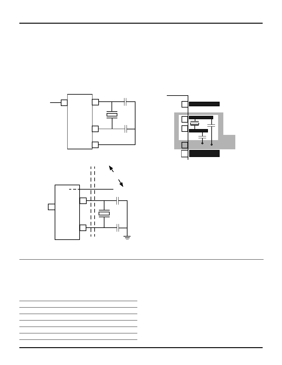
Circuit Board Design Rules
The following circuit board design rules are suggested:
∑
To prevent induced noise, the crystal and load capaci-
tors should be physically located as close to the
Z8Plus as possible.
∑
Signal lines should not run parallel to the clock oscil-
lator inputs. In particular, the crystal input circuitry
and the internal system clock output should be separat-
ed as much as possible.
∑
V
CC
power lines should be separated from the clock
oscillator input circuitry.
∑
Resistivity between
XTAL1
or
XTAL2
(and the other
pins) should be greater than 10 meg-Ohms.
Crystals and Resonators
Crystals and ceramic resonators (Figure 16) should exhibit
the following characteristics to ensure proper oscillation:
Depending on the operation frequency, the oscillator may
require additional capacitors,
C
1
and
C
2
, as illustrated in
Figure 16 and Figure 17. The capacitance values are de-
pendent on the manufacturer's crystal specifications.
Figure 15. Circuit Board Design Rules
XTAL2
V
SS
XTAL1
Board Design Example
V
SS
Z8Plus
Z8Plus
Z8Plus
C
1
C
2
Clock Generator Circuit
Signals A B
Signal C
(Parallel traces
must be avoided)
(Top View)
17
16
15
17
16
XTAL1
XTAL2
X1
X2
PB0
V
CC
Crystal Cut
AT (crystal only)
Mode
Parallel, fundamental mode
Crystal Capacitance
<7pF
Load Capacitance
10pF < CL < 220 pF,
15 typical
Resistance
100 Ohms maximum

Z8PE002
ZiLOG
Z8Plus OTP Microcontroller
DS008700-Z8X0799
P R E L I M I N A R Y
27
In most cases, the
R
D
is 0 Ohms and
R
F
is infinite. These
specifications are determined and specified by the crys-
tal/ceramic resonator manufacturer. The
R
D
can be in-
creased to decrease the amount of drive from the oscillator
output to the crystal. It can also be used as an adjustment
to avoid clipping of the oscillator signal to reduce noise. The
R
F
can be used to improve the start-up of the crystal/ceramic
resonator. The Z8Plus oscillator already locates an internal
shunt resistor in parallel to the crystal/ceramic resonator.
Figure 16, Figure 17, and Figure 18 recommend that the
load capacitor ground trace connect directly to the
V
SS
(GND)
pin of the Z8Plus. This requirement assures that no
system noise is injected into the Z8Plus clock. This trace
should not be shared with any other components except at
the
V
SS
pin of the Z8Plus.
Note: A parallel-resonant crystal or resonator manufacturer
specifies a load capacitor value that is a series combination
of
C
1
and
C
2
, including all parasitics (PCB and holder).
Figure 16. Crystal/Ceramic Resonator Oscillator
Figure 17. LC Clock
XTAL2
Z8Plus
V
SS
XTAL1
C
1
C
2
R
F
R
D
XTAL2
Z8Plus
V
SS
XTAL1
C
1
C
2
L
Figure 18. External Clock
XTAL2
Z8Plus
V
SS
XTAL1
N/C
Z8PE002
Z8Plus OTP Microcontroller
ZiLOG
28
P R E L I M I N A R Y
DS008700-Z8X0799
LC OSCILLATOR
The Z8Plus oscillator can use an inductor capacitor oscil-
lator (
LC
) network to generate an
XTAL
clock (Figure 17).
The frequency stays stable over
V
CC
and temperature. The
oscillation frequency is determined by the equation:
where
L
is the total inductance including parasitics, and
C
T
is the total series capacitance including parasitics.
Simple series capacitance is calculated using the equation
at the top of the next column.
A sample calculation of capacitance
C
1
and
C
2
for 5.83-
MHz frequency and inductance value of 27 µH is displayed
as follows:
Thus,
C
1
= 55.2 pF and
C
2
= 55.2 pF.
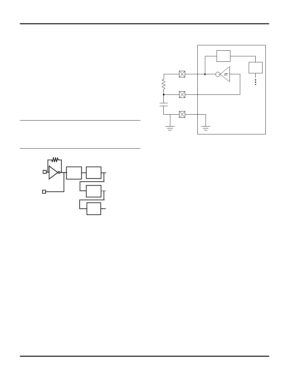
TIMERS
Two 8-bit timers, timer 0 (
T0)
and timer 1 (
T1
) are available
to function as a pair of independent 8-bit standard timers.
They may also be cascaded to function as a 16-bit Pulse-
Width Modulator (PWM) timer. Two additional 8-bit tim-
ers (
T2
and
T3
) are provided, but they can only operate as
one 16-bit standard timer.
Frequency =
1
2
(
LC
T
)
1/2
1/ C
T
= 1/C
1
+ 1/C
2
If C
1
= C
2
1/C
T
= 2/C
1
C
1
= 2C
T
5.83 (10^6) =
1
2
[27 (10
-6
) C
T
]
1/2
C
T
= 27.6 pF
Figure 19. 16-Bit Standard Timer
Enable TCTLL0 (D5)
IRQ5 (T23)
16-bit Down Counter
Internal Data Bus
T2VAL
T3VAL
OSC/8
T3AR
T2AR
Z8PE002
ZiLOG
Z8Plus OTP Microcontroller
DS008700-Z8X0799
P R E L I M I N A R Y
29
Figure 20. 8-Bit Standard Timers
Figure 21. 16-Bit Standard PWM Timer
Enable TCTLL0 (D2≠D0)
IRQ2 (T1)
Internal Data Bus
OSC/8
T1ARHI
T1ARLO
T1VAL
8-bit
Down
Counter
(Not used
in this mode)
8-bit Standard T
imer
Enable TCTLL0 (D2≠D0)
IRQ2 (T0)
Internal Data Bus
OSC/8
T0ARHI
T0ARLO
T0VAL
8-bit
Down
Counter
(Not used
in this mode)
8-bit Standard T
imer
16-Bit Down Counter
Internal Data Bus
High Side
PWM
Low Side
T1ARHI
T1ARLO
IRQ0
IRQ2
T1VAL
T1
T0
Internal Data Bus
T0ARHI
OSC/8
T0ARLO
T0VAL
Edge Detect
Logic
T
OUT
Z8PE002
Z8Plus OTP Microcontroller
ZiLOG
30
P R E L I M I N A R Y
DS008700-Z8X0799
TIMERS (Continued)
A pair of
READ/WRITE
registers is utilized for each 8-bit
timer. One register is defined to contain the auto-initializa-
tion value for the timer. The second register contains the
current value for the timer. When a timer is enabled, the tim-
er decrements the value in its count register and continues
decrementing until it reaches
0
. An interrupt is generated,
and the contents of the auto-initialization register are op-
tionally copied into the count value register. If auto-initial-
ization is not enabled, the timer stops counting when the val-
ue reaches
0
. Control logic clears the appropriate control
register bit to disable the timer. This operation is referred
to as a single-shot. If auto-initialization is enabled, the timer
counts from the initialization value. Software must not at-
tempt to use timer registers for any other function.
User software is allowed to write to any
WRITE
register at
any time; however, care should be taken if timer registers
are updated while the timer is enabled. If software changes
the count value while the timer is in operation, the timer con-
tinues counting from the updated value.
Note: Unpredictable behavior can occur if the value updates at
the same time that the timer reaches
0
.
Similarly, if user software changes the initialization value
register while the timer is active, the next time that the timer
reaches
0
, the timer initializes to the changed value.
Note: Unpredictable behavior can occur if the initialization
value register is changed while the timer is in the process
of being initialized.
The initialization value is determined by the exact timing
of the
WRITE
operation. In all cases, the Z8Plus assigns a
higher priority to the software
WRITE
than to a decrementer
write-back. However, when hardware clears a control reg-
ister bit for a timer that is configured for single-shot oper-
ation, the clearing of the control bit overrides a software
WRITE
. A
READ
of either register can be conducted at any
time, with no effect on the functionality of the timer.
Figure 22. TCTLLO Register
D7
D6
D5
D4
D3
D2
D1
D0
0C0
TCTLLO
TIMER STATUS
D2
D1
D0
T0
T1
T01
----
----
---- -------------
-------------
---------------
0
0
0
Disabled
Disabled
0
0
1
Enabled
Disabled
0
1
0
Disabled
Enabled
0
1
1
Enabled
Enabled
1
0
0
Enabled*
1
0
1
Enabled*
Disabled
1
1
0
Disabled
Enabled*
1
1
1
Enabled*
Enabled*
N
OTE
:
(*) indicates auto-reload is active.
Reserved (must be 0)
1 = T23 16-Bit Timer Enabled with Auto-Reload Active
0 = T2 and T3 Timers Disabled
Reserved (must be 0)
Note:
Timer T01 is a 16-bit PWM Timer formed by cascading 8-bit timers
T1 (MSB) and T0 (LSB). T23 is a standard 16-bit timer formed
by cascading 8-bit timers T3 (MSB) and T2 (LSB).

Z8PE002
ZiLOG
Z8Plus OTP Microcontroller
DS008700-Z8X0799
P R E L I M I N A R Y
31
If a timer pair is defined to operate as a single 16-bit entity,
the entire 16-bit value must reach
0
before an interrupt is
generated. In this case, a single interrupt is generated, and
the interrupt corresponds to the even 8-bit timer.
Example:
Timers
T2
and
T3
are cascaded to form a single 16-
bit timer. The interrupt for the combined timer is
defined to be generated by timer
T2
rather than
T3
.
When a timer pair is specified to act as a single 16-
bit timer, the even timer registers in the pair (timer
T0
or
T2
) is defined to hold the timer's least
significant byte. In contrast, the odd timer in the pair
holds the timer's most significant byte.
In parallel with the posting of the interrupt request, the in-
terrupting timer's count value is initialized by copying the
contents of the auto-initialization value register to the count
value register.
Note:
Any time that a timer pair is defined to act as a single 16-
bit timer, the auto-reload function is performed automat-
ically.
All 16-bit timers continue counting while their interrupt re-
quests are active and operate independently of each other.
If interrupts are disabled for a long period of time, it is pos-
sible for the timer to decrement to
0
again before its initial
interrupt is responded to. This condition is termed a degen-
erate case, and hardware is not required to detect it.
When the timer control register is written, all timers that are
enabled by the
WRITE
begin counting from the value in the
count register. In this case, an auto-initialization is not per-
formed. All timers can receive an internal clock source input
only. Each enabled timer is updated every 8th
XTAL
clock
cycle.
If
T0
and
T1
are defined to work independently, then each
works as an 8-bit timer with a single auto-initialization reg-
ister (
T0ARLO
for
T0
, and
T1ARLO
for
T1
). Each timer as-
serts its predefined interrupt when it times out, optionally
performing the auto-initialization function. If
T0
and
T1
are
cascaded to form a single 16-bit timer, then the single 16-
bit timer is capable of performing as a Pulse-Width Mod-
ulator (PWM). This timer is referred to as
T01
to distinguish
it as having special functionality that is not available when
T0
and
T1
act independently.
When
T01
is enabled, it can use a pair of 16-bit auto-ini-
tialization registers. In this mode, one 16-bit auto-initial-
ization value is composed of the concatenation of
T1ARLO
and
T0ARLO
. The second auto-initialization value is com-
posed of the concatenation of
T1ARHI
and
T0ARHI
. When
T01
times out, it alternately initializes its count value using
the Low auto-init pair, followed by the High auto-init pair.
This functionality corresponds to a PWM. That is, the
T1
interrupt defines the end of the High section of the wave-
form, and the
T0
interrupt marks the end of the Low portion
of the PWM waveform.
The PWM begins counting with whatever data is held in the
count registers. After this value expires, the first reload de-
pends on the state of the
PB1
pin if
T
OUT
mode is selected.
Otherwise, the Low value is applied first.
After the auto-initialization is completed, decrementing oc-
curs for the number of counts defined by the
PWM_LO
reg-
isters. When decrementing again reaches
0
, the
T0
interrupt
is asserted; and auto-init using the
PWM_HI
registers oc-
curs. Decrementing occurs for the number of counts defined
by the
PWM_HI
registers until reaching
0
. From there, the
T1
interrupt
IRQ2
is asserted, and the cycle begins again.
The internal timers can be used to trigger external events
by toggling the
PB1
output when generating an interrupt.
This functionality can only be achieved in conjunction with
the port unit defining the appropriate pin as an output signal
with the timer output special function enabled. In this mode,
the port output is toggled when the timer count reaches
0
,
and continues toggling each time that the timer times out.
T
OUT
Mode
The PortB special function register
PTBSFR
(
0D7H
; Figure
23) is used in conjunction with the Port B directional control
register
PTBDIR
(
0D6
; Figure 24) to configure
PB1
for
T
OUT
operation for
T0
. In order for
T
OUT
to function,
PB1
must
be defined as an output line by setting
PTBDIR
bit 1 to
1
.
Configured in this way,
PB1
is capable of being a clock
output for
T0
, toggling the
PB1
output pin on each
T0
time-
out.
At end-of-count, the interrupt request line (
IRQ0
), clocks a
toggle flip-flop. The output of this flip-flop drives the
T
OUT
line,
PB1
. In all cases, when
T0
reaches its end-of-count,
T
OUT
toggles to its opposite state (Figure 25). If, for exam-
ple,
T0
is in Continuous Counting Mode,
T
OUT
exhibits a
50-percent duty cycle output. If the timer pair is selected
(
T01
) as a PWM, the duty cycle depends on the High and
Low reload values. At the end of each High time,
PB1
tog-
gles Low. At the end of each Low time,
PB1
toggles HI.
Z8PE002
Z8Plus OTP Microcontroller
ZiLOG
32
P R E L I M I N A R Y
DS008700-Z8X0799
TIMERS (Continued)
Figure 23. PortB Special Function Register
Figure 24. Port B Directional Control Register
Figure 25. Timer T0 Output Through T
OUT
D7
D6
D5
D4
D3
D2
D1
D0
0D7
PTBSFR
1 = Enable Bit 0 as SMR input
0 = No special functionality
1 = Enable Bit 1 as
T0
output
0 = No special functionality
1 = Enable Bit 2 as IRQ2 input
0 = No special functionality
D4 D3 Comparator Interrupts
--- --- -------------- -------------------
0 0 Disabled
Disabled
0 1 Enabled
Disabled
1 0 Disabled
Enabled
1 1 Enabled
Enabled
BIT 3: Comparator reference input
BIT 4: Comparator signal input/IRQ0/IRQ2
Reserved (must be 0)
D7
D6
D5
D4
D3
D2
D1
D0
0D6
PTBDIR
Reserved (must be 0)
1 = Bit n set as output
0 = Bit n set as input
T
OUT
PB1
IRQ0
(T0 End-of-Count)
˜
2
Z8PE002
ZiLOG
Z8Plus OTP Microcontroller
DS008700-Z8X0799
P R E L I M I N A R Y
33
RESET CONDITIONS
After a
RESET
, the timers are disabled. See Table 8 for timer
control, value, and auto-initialization register status after
RESET
.
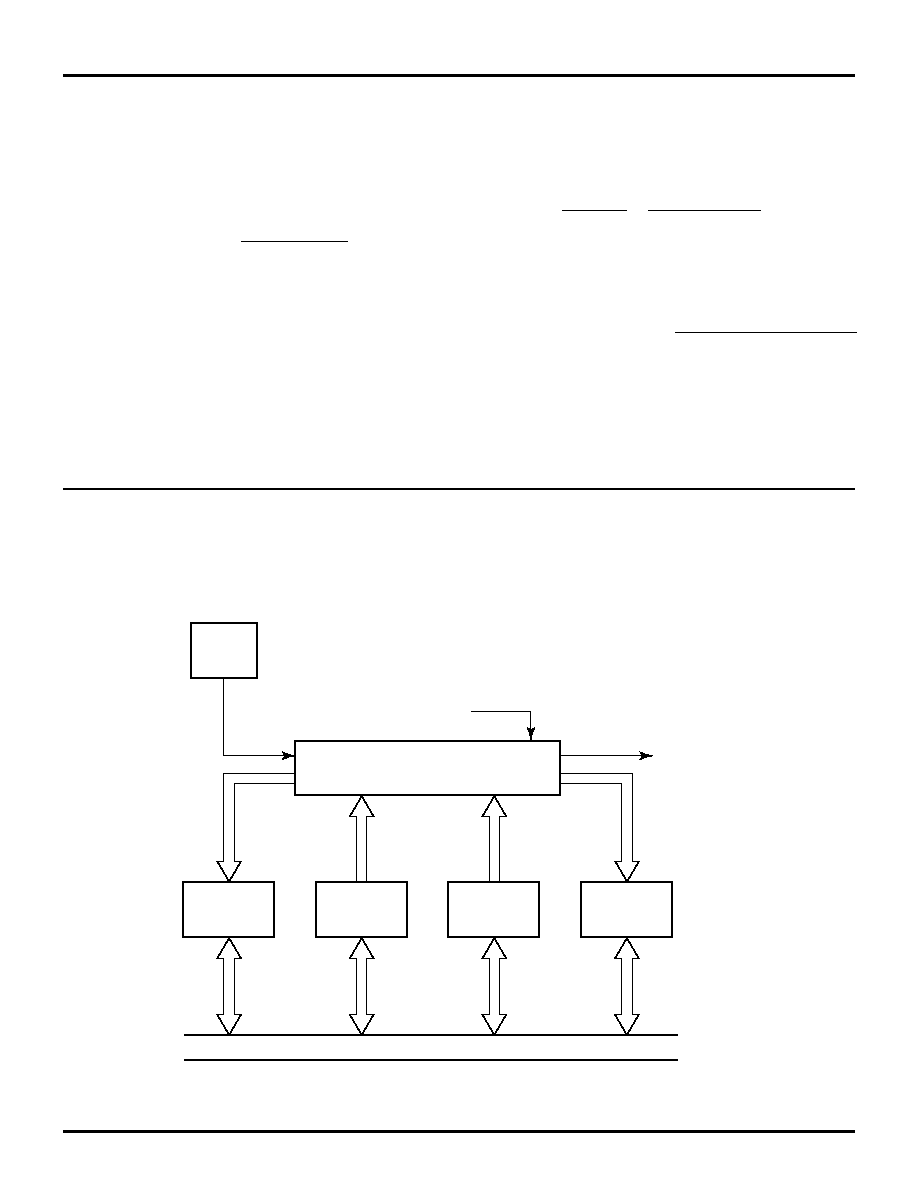
I/O PORTS
The Z8Plus
dedicates 14 lines to input and output. These lines
are grouped into two ports known as Port A and Port B. Port
A is an 8-bit port, bit programmable as either inputs or outputs.
Port B can be programmed to provide either standard in-
put/output, or the following special functions:
T0
output,
comparator input,
SMR
input, and external interrupt inputs.
All pins except
PB5
include push-pull CMOS outputs. In
addition, the outputs of Port A on a bit-wise basis can be
configured for open-drain operation.The ports operate on
a bit-wise basis. As such, the register values for/at a given
bit position only affect the bit in question.
Each port is defined by a set of four control registers (Figure 26).
Directional Control and Special Function
Registers
Each port on the Z8Plus features a dedicated directional con-
trol register that determines (on a bit-wise basis) if a given
port bit operates as input or output.
Each port on the Z8Plus features a special function register
(
SFR
) that, in conjunction with the directional control reg-
ister, implements (on a bit-by-bit basis) any special func-
tionality that can be defined for each particular port bit.
Input and Output Value Registers
Each port features an Output Value Register and an input
value register. For port bits configured as an input by means
of the directional control register, the input value register
Figure 26. Port A Configuration with Open-Drain Capability and Schmitt-Trigger
PIN
PA0≠PA7
PTAIN Bit n
N = 0...7
PTAOUT Bit n
N = 0...7
PTASFR Bit n
N = 0...7
PTADIR Bit n
N = 0...7
Table 14. I/O Ports Registers
Register
Address
Identifier
Port B Special Function
0D7H
PTBSFR
Port B Directional Control
0D6H
PTBDIR
Port B Output Value
0D5H
PTBOUT
Port B Input Value
0D4H
PTBIN
Port A Special Function
0D3H
PTASFR
Port A Directional Control
0D2H
PTADIR
Port A Output Value
0D1H
PTAOUT
Port A Input Value
0D0H
PTAIN

Z8PE002
Z8Plus OTP Microcontroller
ZiLOG
34
P R E L I M I N A R Y
DS008700-Z8X0799
for that bit position contains the current synchronized input
value.
For port bits configured as an output by means of the di-
rectional control register, the value held in the correspond-
ing bit of the Output Value Register is driven directly onto
the output pin. The opposite register bit for a given pin (the
output register bit for an input pin and the input register bit
for an output pin) holds their previous value. These bits are
not changed and do not exhibit any effect on the hardware.
READ/WRITE OPERATIONS
The control for each port is done on a bit-by-bit basis. All
bits are capable of operating as inputs or outputs, depending
on the setting of the port's directional control register. If
configured as an input, each bit is provided a Schmitt-trig-
ger. The output of the Schmitt-trigger is latched twice to
perform a synchronization function, and the output of the
synchronizer is fed to the port input register, which can be
read by software.
A
WRITE
to a port input register carries the effect of up-
dating the contents of the input register, but subsequent
READs
do not necessarily return the same value that was
written. If the bit in question is defined as an input, the input
register for that bit position contains the current synchro-
nized input value.
WRITEs
to that bit position are overwrit-
ten on the next clock cycle with the newly sampled input
data. However, if the particular bit is programmed as an out-
put, the input register for that bit retains the software-up-
dated value. The port bits that are programmed as outputs
do not sample the value being driven out.
Any bit in either port can be defined as an output by setting
the appropriate bit in the directional control register. In this
instance, the value held in the appropriate bit of the port out-
put register is driven directly onto the output pin.
Note:
The preceding result does not necessarily reflect the actual
output value. If an external error is holding an output pin ei-
ther High or Low against the output driver, the software
READ
returns the
requested
value, not the actual state
caused by the contention. When a bit is defined as an output,
the Schmitt-trigger on the input is disabled to save power.
Updates to the output register take effect based on the timing
of the internal instruction pipeline; however, this timing is
referenced to the rising edge of the clock. The output reg-
ister can be read at any time, and returns the current output
value that is held. No restrictions are placed on the timing
of
READs
and/or
WRITEs
to any of the port registers with
respect to the others.
Note: Care should be taken when updating the directional con-
trol and special function registers.
When updating a directional control register, the special
function register (
SFR
) should first be disabled. If this pre-
caution is not taken, unpredicted events could occur as a re-
sult of the change in the port I/O status. This precaution is
especially important when defining changes in Port B, as
the unpredicted event referred to above could be one or
more interrupts. Clearing of the
SFR
register should be the
first step in configuring the port, while setting the
SFR
reg-
ister should be the final step in the port configuration pro-
cess. To ensure unpredictable results, the
SFR
register
should not be written until the pins are being driven appro-
priately, and all initialization is completed.
PORT A
Port A is a general-purpose port. Figure 27 features a block
diagram of Port A. Each of its lines can be independently
programmed as input or output via the Port A directional
control register (
PTADIR
at
0D2H
) as seen in Figure 26. A
bit set to a
1
in
PTADIR
configures the corresponding bit in
Port A as an output, while a bit cleared to
0
configures the
corresponding bit in Port A as an input.
The input buffers are Schmitt-triggered. Bits programmed
as outputs can be individually programmed as either push-
pull or open-drain by setting the corresponding bit in the
special function register (
PTASFR
, Figure 26).
Figure 27. Port A Directional Control Register
D7 D6 D5 D4 D3 D2 D1 D0
0 = Input
1 = Output
PTADIR Register
Register 0D2H
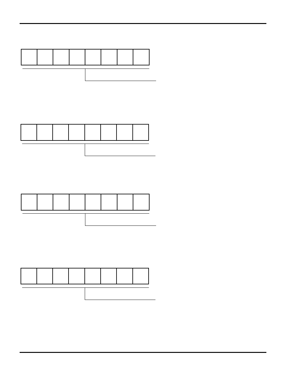
Z8PE002
ZiLOG
Z8Plus OTP Microcontroller
DS008700-Z8X0799
P R E L I M I N A R Y
35
PORT A REGISTER DIAGRAMS
Figure 28. Port A Input Value Register
Figure 29. Port A Output Value Register
Figure 30. Port A Directional Control Register
Figure 31. Port A Special Function Register
D7
D6
D5
D4
D3
D2
D1
D0
Register 0D0H
PTAIN
Port A Bit n current input value
(only updated for pins in input mode)
D7
D6
D5
D4
D3
D2
D1
D0
Register 0D1H
PTAOUT
Port A Bit n currentoutput value
D7
D6
D5
D4
D3
D2
D1
D0
Register 0D2H
PTADIR
1 = Bit n set as an output
0 = Bit n set as an input
D7
D6
D5
D4
D3
D2
D1
D0
Register 0D3H
PTASFR
1 = Bit n in open-drain mode
0 = Bit n in push-pull mode

Z8PE002
Z8Plus OTP Microcontroller
ZiLOG
36
P R E L I M I N A R Y
DS008700-Z8X0799
PORT B
Port B Description
Port B is a 6-bit (bidirectional), CMOS-compatible I/O port.
These six I/O lines can be configured under software control
to be an input or output. Each bit is configured
independently from the other bits. That is, one bit may be
set to
INPUT
while another bit is set to
OUTPUT
.
In addition to standard input/output capability, five pins of
Port B provide special functionality as indicated in Table 15.
Special functionality is invoked via the Port B special func-
tion register. Port B, bit 5, is an open-drain-only pin when
in output mode. There is no high-side driver on the output
stage, nor is there any high-side protection device, because
PB5
acts as the
V
PP
pin for EPROM programming mode.
The user should always place an external protection diode
on this pin. See Figure 32.
Table 15. Port B Special Functions
Port
Pin
Input Special
Function
Output Special
Function
PB0
Stop Mode Recovery
Input
None
PB1
None
T0 Output
PB2
IRQ3
None
PB3
Comparator
Reference Input
None
PB4
Comparator Signal
Input/IRQ1/IRQ4
None
Figure 32. Port B Special Function Register
D7
D6
D5
D4
D3
D2
D1
D0
Register 0D7H
PTBSFR
1 = Enable PB0 as SMR Input
0 = No Special Functionality
1 = Enable PB1 as T0 Output
0 = No Special Functionality
1 = Enable PB2 as IRQ3 Input
0 = No Special Functionality
Reserved (must be 0)
1 = Analog Comparator on PB3 and PB4
0 = Digital Inputs on PB3 and PB4
1 = PB4 Interrupts Enabled
0 = PB4 Interrupts Disabled

Z8PE002
ZiLOG
Z8Plus OTP Microcontroller
DS008700-Z8X0799
P R E L I M I N A R Y
37
PORT B--PIN 0 CONFIGURATION
Figure 33. Port B Pin 0 Diagram
Figure 34. Port B Pin 5 Diagram
PIN
PB0
PTBOUT Bit 0
PTBSFR Bit 0
PTBDIR Bit 0
PTBDIR Bit 0
PTBIN Bit 0
SMR
SMR Flag
RESET
PB5
PTBOUT Bit 5
PTBDIR Bit 5
PTBDIR Bit 5
PTBIN Bit 5
PIN
approx 200 kOhms
V
See Note
Note: There is no high-side protection device. The user should always place an external protection diode as shown.
CC

Z8PE002
Z8Plus OTP Microcontroller
ZiLOG
38
P R E L I M I N A R Y
DS008700-Z8X0799
PORT B--PIN 1 CONFIGURATION
Figure 35. Port B Pin 1 Diagram
PIN
PB1
T0 Output
PTBOUT Bit 1
PTBSFR Bit 1
PTBDIR Bit 1
PTBDIR Bit 1
PTBIN Bit 1
M
U
X
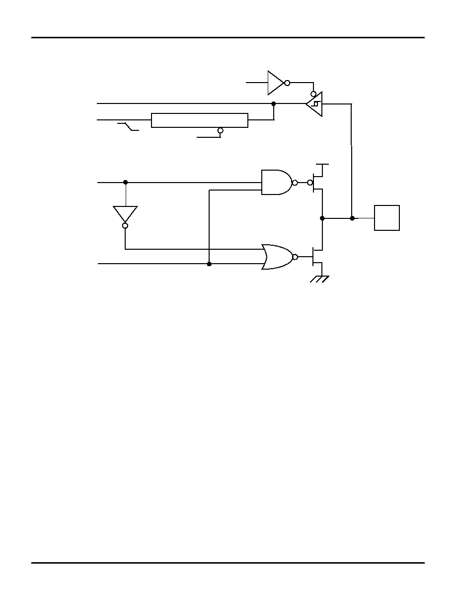
Z8PE002
ZiLOG
Z8Plus OTP Microcontroller
DS008700-Z8X0799
P R E L I M I N A R Y
39
PORT B--PIN 2 CONFIGURATION
Figure 36. Port B Pin 2 Diagram
PIN
PB2
PTBOUT Bit 2
PTBSFR Bit 2
PTBDIR Bit 2
PTBDIR Bit 2
PTBIN Bit 2
Edge Detect Logic
IRQ3

Z8PE002
Z8Plus OTP Microcontroller
ZiLOG
40
P R E L I M I N A R Y
DS008700-Z8X0799
PORT B--PINS 3 AND 4 CONFIGURATION
Figure 37. Port B Pins 3 and 4 Diagram
PIN
PB3
PTBOUT Bit 3
PTBSFR Bit 3
PTBDIR Bit 3
PTBDIR Bit 4
PTBIN Bit 4
Edge Detect Logic
IRQ1
IRQ4
+
AN IN
REF
PTBDIR Bit 3
PTBIN Bit 3
PIN
PB4
PTBOUT Bit 4
PTBDIR Bit 4
PTBSFR Bit 4
M
U
X
-
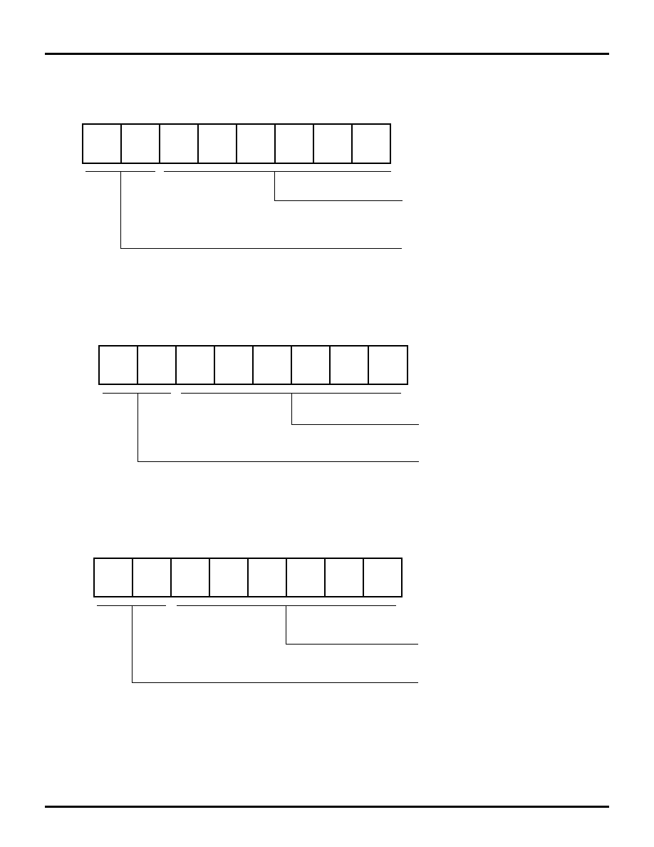
Z8PE002
ZiLOG
Z8Plus OTP Microcontroller
DS008700-Z8X0799
P R E L I M I N A R Y
41
PORT B CONTROL REGISTERS
Figure 38. Port B Input Value Register
Figure 39. Port B Output Value Register
Figure 40. Port B Directional Control Register
D7
D6
D5
D4
D3
D2
D1
D0
Register 0D4H
PTBIN
Port B Bit n current input value
Reserved (must be 0)
(only updated for pins in input mode)
D7
D6
D5
D4
D3
D2
D1
D0
Register 0D5H
PTBOUT
Port B Bit n current output value
Reserved (must be 0)
D7
D6
D5
D4
D3
D2
D1
D0
Register 0D6H
PTBDIR
Reserved (must be 0)
1 = Bit n set as output
0 = Bit n set as input

Z8PE002
Z8Plus OTP Microcontroller
ZiLOG
42
P R E L I M I N A R Y
DS008700-Z8X0799
PORT B CONTROL REGISTERS (Continued)
Figure 41. Port B Special Function Register
D7
D6
D5
D4
D3
D2
D1
D0
Register 0D7H
PTBSFR
1 = Enable PB0 as SMR Input
0 = No Special Functionality
1 = Enable PB1 as T0 Output
0 = No Special Functionality
1 = Enable PB2 as IRQ3 Input
0 = No Special Functionality
Reserved (must be 0)
1 = Analog Comparator on PB3 and PB4
0 = Digital Inputs on PB3 and PB4
1 = PB4 Interrupts Enabled
0 = PB4 Interrupts Disabled

Z8PE002
ZiLOG
Z8Plus OTP Microcontroller
DS008700-Z8X0799
P R E L I M I N A R Y
43
I/O PORT RESET CONDITIONS
Full Reset
Port A and Port B output value registers are not affected by
RESET
.
On
RESET
, the Port A and Port B directional control reg-
isters are cleared to all zeros, which defines all pins in both
ports as inputs.
On
RESET
, the directional control registers redefine all pins
as inputs, and the Port A and Port B input value registers
overwrites the previously held data with the current sample
of the input pins.
On
RESET
, the Port A and Port B special function registers
are cleared to
00h
, which deactivates all port special func-
tions.
Note: The
SMR
and
WDT
time-out events are
not
full device
resets. The port control registers are not affected by ei-
ther of these events.
ANALOG COMPARATOR
The device includes one on-chip analog comparator. Pin
PB4
features a comparator front end. The comparator ref-
erence voltage is on pin
PB3
.
Comparator Description
The on-chip comparator can process an analog signal on
PB4
with reference to the voltage on
PB3
. The analog func-
tion is enabled by programming the Port B special function
register bits 3 and 4.
When the analog comparator function is enabled, bit 4 of
the input register is defined as holding the synchronized out-
put of the comparator, while bit 3 retains a synchronized
sample of the reference input.
If the interrupts for
PB4
are enabled when the comparator
special function is selected, the output of the comparator
generates interrupts.
COMPARATOR OPERATION
The comparator output reflects the relationship between the
analog input to the reference input. If the voltage on the an-
alog input is higher than the voltage on the reference input,
then the comparator output is at a High state. If the voltage
on the analog input is lower than the voltage on the reference
input, then the analog output is at a Low state.
Comparator Definitions
V
ICR
The usable voltage range for the positive input and
reference input is called the Comparator Input Common
Mode Voltage Range (
V
ICR
).
Note: The comparator is not guaranteed to work if the input is
outside of the
V
ICR
range.
V
OFFSET
The absolute value of the voltage between the positive input
and the reference input required to make the comparator
output voltage switch is the Comparator Input Offset Volt-
age (
V
OFFSET
).
I
IO
For the CMOS voltage comparator input, the input offset current
(
I
IO
) is the leakage current of the CMOS input gate.
HALT Mode
The analog comparator is functional during
HALT
mode. If
the interrupts are enabled, an interrupt generated by the
comparator causes a return from
HALT
mode.
STOP Mode
The analog comparator is disabled during
STOP
mode. The
comparator is powered down to prevent it from drawing any
current.
Low Voltage Protection.
An on-board Voltage Compar-
ator checks that the
V
CC
is at the required level to ensure
correct operation of the device. A reset is globally driven
if
V
CC
is below the specified voltage (Low Voltage Protec-
tion).
The device functions normally at or above 3.0V under all
conditions, and is guaranteed to function normally at supply
voltages above the Low Voltage Protection trip point. Be-
low 3.0V, the device functions normally until the Low Volt-
Z8PE002
Z8Plus OTP Microcontroller
ZiLOG
44
P R E L I M I N A R Y
DS008700-Z8X0799
COMPARATOR OPERATION (Continued)
age Protection trip point (
V
LV
) is reached. The actual Low-
Voltage Protection trip point is a function of process pa-
rameters.
Low-Voltage Protection is active in
RUN
and
HALT
modes
only, but is disabled in
STOP
mode (Figure 42).
Figure 42. Voltage vs. Temperature
V
CC
Volts)
2.80
2.40
2.20
2.00
1.80
1.60
≠60
≠40
≠20
0
20
40
60
80
100
120
140
3.00
2.60
Temperature (∫C)
Typical V
in RUN and
HALT modes
LV

Z8PE002
ZiLOG
Z8Plus OTP Microcontroller
DS008700-Z8X0799
P R E L I M I N A R Y
45
INPUT PROTECTION
All I/O pins feature diode input protection. There is a diode
from the I/O pad to
V
CC
and
V
SS
(Figure 43).
However, the
PB5
pin features only the input protection di-
ode, from the pad to
V
SS
(Figure 44).
The high-side input protection diode was removed on this
pin to allow the application of high voltage during the OTP
programming mode.
For better noise immunity in applications that are exposed
to system EMI, a clamping diode to
V
SS
from this pin should
be used to prevent entering the OTP programming mode or
to prevent high voltage from damaging this pin.
Figure 43. I/O Pin Diode Input Protection
PIN
V
CC
V
SS
Figure 44. PB5 Pin Input Protection
PIN
V
SS
PB5
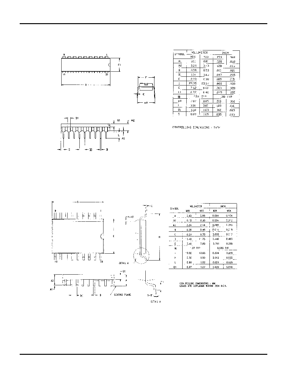
Z8PE002
Z8Plus OTP Microcontroller
ZiLOG
46
P R E L I M I N A R Y
DS008700-Z8X0799
PACKAGE INFORMATION
Figure 45. 18-Pin DIP Package Diagram
Figure 46. 18-Pin SOIC Package Diagram
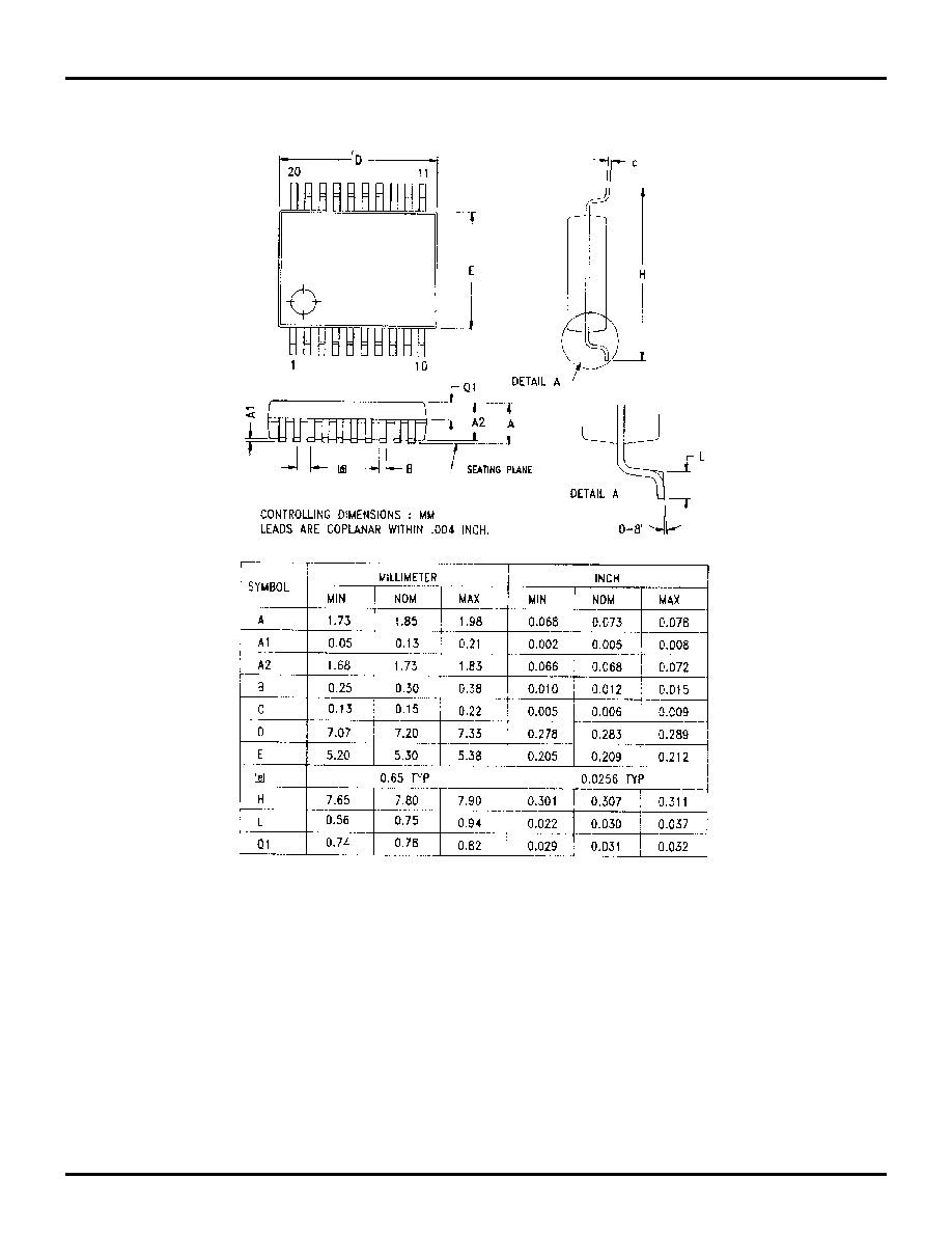
Z8PE002
ZiLOG
Z8Plus OTP Microcontroller
DS008700-Z8X0799
P R E L I M I N A R Y
47
Figure 47. 20-Pin SSOP Package Diagram

Z8PE002
Z8Plus OTP Microcontroller
ZiLOG
48
P R E L I M I N A R Y
DS008700-Z8X0799
ORDERING INFORMATION
For fast results, contact your local ZiLOG sales office for
assistance in ordering the part(s) required.
Example:
The Z8PE002PZ010SC is a 10-MHz DIP, 0∫C to 70∫C, with Plastic Standard Flow.
Pre-Characterization Product
The product represented by this document is newly introduced
and ZiLOG has not completed the full characterization of the
product. The document states what ZiLOG knows about this
product at this time, but additional features or non-conformance
with some aspects of the document may be found, either by
ZiLOG or its customers in the course of further application and
characterization work. In addition, ZiLOG cautions that delivery
may be uncertain at times, due to start-up yield issues.
©1999 by ZiLOG, Inc. All rights reserved. Information in this
publication concerning the devices, applications, or technology
described is intended to suggest possible uses and may be
superseded. ZiLOG, INC. DOES NOT ASSUME LIABILITY
FOR OR PROVIDE A REPRESENTATION OF ACCURACY
OF THE INFORMATION, DEVICES, OR TECHNOLOGY
DESCRIBED IN THIS DOCUMENT. ZiLOG ALSO DOES
NOT ASSUME LIABILITY FOR INTELLECTUAL
PROPERTY INFRINGEMENT RELATED IN ANY
MANNER TO USE OF INFORMATION, DEVICES, OR
TECHNOLOGY DESCRIBED HEREIN OR OTHERWISE.
Except with the express written approval of ZiLOG, use of
information, devices, or technology as critical components of
life support systems is not authorized. No licenses are conveyed,
implicitly or otherwise, by this document under any intellectual
property rights.
ZiLOG, Inc.
910 East Hamilton Avenue, Suite 110
Campbell, CA 95008
Telephone (408) 558-8500
FAX 408 558-8300
Internet:
http://www.zilog.com
Standard Temperature
18-Pin DIP
Z8PE002PZ010SC
18-Pin SOIC
Z8PE002SZ010SC
20-Pin SSOP
Z8PE002HZ010SC
Extended Temperature
18-Pin DIP
Z8PE002PZ010EC
18-Pin SOIC
Z8PE002SZ010EC
20-Pin SSOP
Z8PE002CZ010EC
Codes
Preferred Package
PZ = Plastic DIP
Longer Lead Time
SZ = SOIC
HZ = SSOP
Speed
010 = 10 MHz
Standard Temperature
S = 0∞C to +70∞C
Extended Temperature
E = ≠40∞C to +105∞C
Environmental Flow
C = Plastic Standard
Z
ZiLOG Prefix
8PE
Z8Plus Product
002
Product Number
PZ
Package Designation Code
010
Speed
SC
Temperature and Environmental Flow