DS971800401
P R E L I M I N A R Y
1-1
1
P
RELIMINARY
P
RODUCT
S
PECIFICATION
Z80180/Z8S180/
1
Z8L180 SL1919
E
NHANCED
Z180 M
ICROPROCESSOR
FEATURES
s
Code Compatible with Zilog Z80
�
CPU
s
Extended Instructions
s
Two Chain-Linked DMA Channels
s
Low Power-Down Modes
s
On-Chip Interrupt Controllers
s
Three On-Chip Wait-State Generators
s
On-Chip Oscillator/Generator
s
Expanded MMU Addressing (up to 1 MB)
s
Clocked Serial I/O Port
s
Two 16-Bit Counter/Timers
s
Two Enhanced UARTs (up to 512 Kbps)
s
Clock Speeds: 6, 8, 10, 20, 33 MHz
s
Operating Range: 5V (3.3V@ 20 MHz)
s
Operating Temperature Range: 0
�
C to +70
�
C
s
-40
�
C to +85
�
C Extended Temperature Range
s
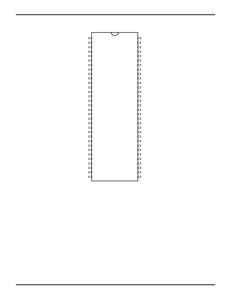
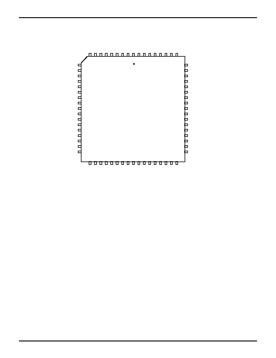
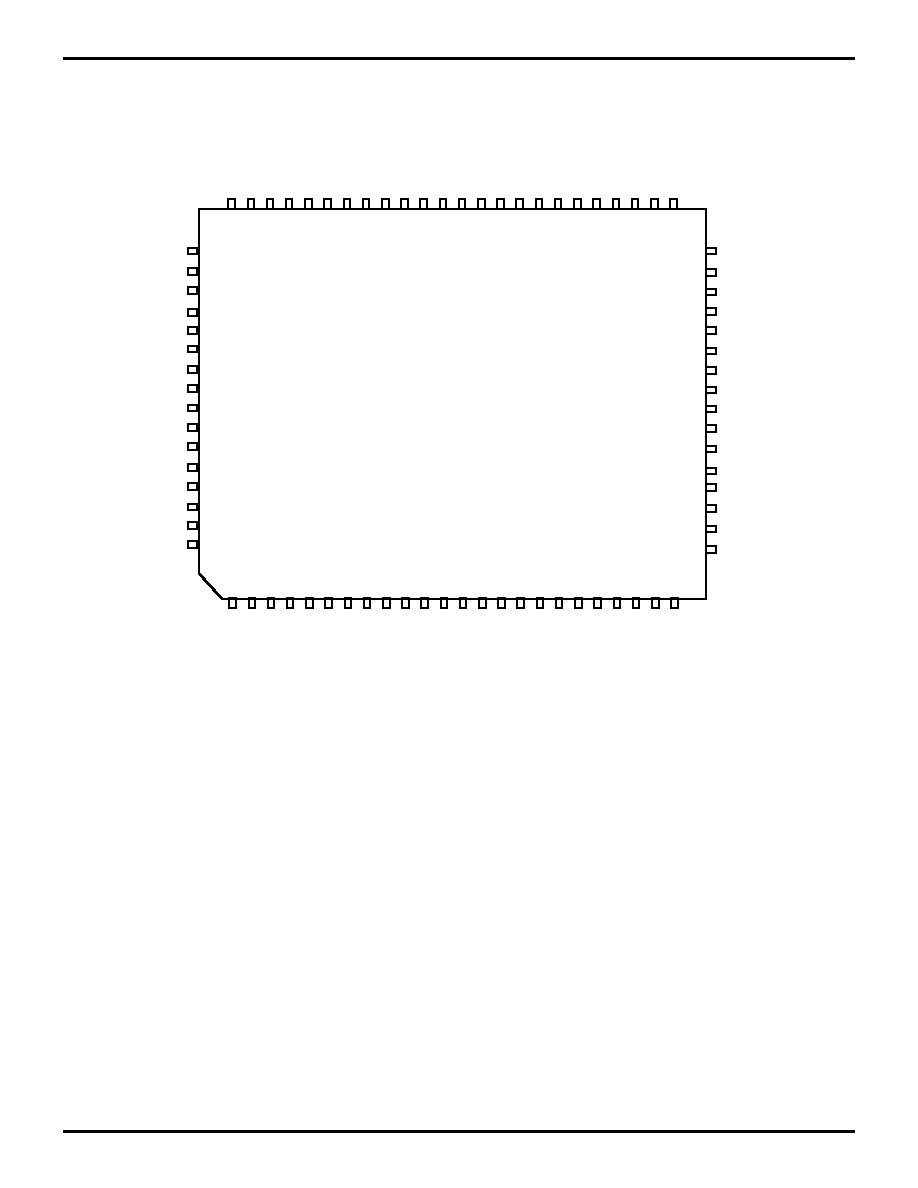
Three Packaging Styles
�
68-Pin PLCC
�
64-Pin DIP
�
80-Pin QFP
GENERAL DESCRIPTION
The enhanced Z80180/Z8S180/Z8L180
TM
significantly im-
proves on the previous Z80180 models while still providing
full backward compatibility with existing Zilog Z80 devices.
The Z80180/Z8S180/Z8L180 now offers faster execution
speeds, power saving modes, and EMI noise reduction.
This enhanced Z180 design also incorporates additional
feature enhancements to the ASCIs, DMAs, and I
cc
STANDBY Mode power consumption. With the addition of
"ESCC-like" Baud Rate Generators (BRGs), the two ASCIs
now have the flexibility and capability to transfer data asyn-
chronously at rates of up to 512 Kbps. In addition, the ASCI
receiver has added a 4-byte First In First Out (FIFO) which
can be used to buffer incoming data to reduce the inci-
dence of overrun errors. The DMAs have been modified to
allow for a "chain-linking" of the two DMA channels when
set to take their DMA requests from the same peripherals
device. This feature allows for non-stop DMA operation be-
tween the two DMA channels, reducing the amount of CPU
intervention (Figure 1).
Not only does the Z80180/Z8S180/Z8L180 consume less
power during normal operations than the previous model,
it has also been designed with three modes intended to fur-
ther reduce the power consumption. Zilog reduced I
cc
pow-
er consumption during STANDBY Mode to a minimum of
10
�
A by stopping the external oscillators and internal
clock. The SLEEP mode reduces power by placing the
CPU into a "stopped" state, thereby consuming less cur-
rent while the on-chip I/O device is still operating. The
SYSTEM STOP mode places both the CPU and the on-
chip peripherals into a "stopped" mode, thereby reducing
power consumption even further.
A new clock doubler feature has been implemented in the
Z80180/Z8S180/Z8L180 device that allows the program-
mer to double the internal clock from that of the external
clock. This provides a systems cost savings by allowing
the use of lower cost, lower frequency crystals instead of
the higher cost, and higher speed oscillators.
The Enhanced Z180 is housed in 80-pin QFP, 68-pin
PLCC, and 64-pin DIP packages.
Z80180/Z8S180/Z8L180
Enhanced Z180 Microprocessor
Zilog
1-2
P R E L I M I N A R Y
DS971800401
Notes:
All Signals with a preceding front slash, "/" are ac-
tive Low, for example, B//W (WORD is active Low); /B/W
(BYTE is active Low, only). Alternatively, an overslash
may be used to signify active Low, for example WR
Power connections follow conventional descriptions be-
low:
Connection
Circuit
Device
Power
V
CC
V
DD
Ground
GND
V
SS
Figure 1. Z80180/Z8S180/Z8L180 Functional Block Diagram
16-bit
Programmable
Reload Timers
(2)
Clocked
Serial I/O
Port
MMU
Bus State Control
CPU
Interrupt
/RESET
/RD
/WR
/M1
/MREQ
IORQ
/HAL
T
/W
AIT
/BUSREQ
/BUSACK
/RFSH
ST
E
/NMI
INT0
INT1
INT2
TXS
RXS/CTS1
CKS
A18/TOUT
DMAC
S
(2)
Asynchronous
SCI
(Channel 0)
Asynchronous
SCI
(Channel 1)
/DREQ1
TEND1
TXA0
CKA0, /DREQ0
RXA0
/RTS0
/CTS0
/DCD0
TXA1
CKA1, /TEND0
RXA1
Timing
Generator
XT
AL
EXT
AL
�
Data
Buffer
Address
Buffer
VCC
VSS
A19-A0
D7-D0
Data Bus (8-Bit)
Address Bus (16-Bit)