 | –≠–ª–µ–∫—Ç—Ä–æ–Ω–Ω—ã–π –∫–æ–º–ø–æ–Ω–µ–Ω—Ç: Z90251 | –°–∫–∞—á–∞—Ç—å:  PDF PDF  ZIP ZIP |

ZiLOG W
ORLDWIDE
H
EADQUARTERS
• 910 E. H
A
milton Avenue • Campbell, CA 95008
Telephone: 408.558.8500 • Fax: 408.558.8300 • www.ZiLOG.com
Z90255 ROM and Z90251 OTP
32 KB Television Controller
with OSD
Product Specification
PS001301-0800

This publication is subject to replacement by a later edition. To determine
whether a later edition exists, or to request copies of publications, contact
ZiLOG Worldwide Headquarters
910 E. Hamilton Avenue
Campbell, CA 95008
Telephone: 408.558.8500
Fax: 408.558.8300
www.ZiLOG.com
Windows is a registered trademark of Microsoft Corporation.
Document Disclaimer
© 2000 by ZiLOG, Inc. All rights reserved. Information in this publication concerning the devices, applications, or
technology described is intended to suggest possible uses and may be superseded. ZiLOG, INC. DOES NOT
ASSUME LIABILITY FOR OR PROVIDE A REPRESENTATION OF ACCURACY OF THE INFORMATION, DEVICES,
OR TECHNOLOGY DESCRIBED IN THIS DOCUMENT. ZiLOG ALSO DOES NOT ASSUME LIABILITY FOR
INTELLECTUAL PROPERTY INFRINGEMENT RELATED IN ANY MANNER TO USE OF INFORMATION, DEVICES,
OR TECHNOLOGY DESCRIBED HEREIN OR OTHERWISE. Except with the express written approval ZiLOG, use of
information, devices, or technology as critical components of life support systems is not authorized. No licenses or
other rights are conveyed, implicitly or otherwise, by this document under any intellectual property rights.

Z90255 ROM and Z90251 OTP
32 KB Television Controller with OSD
PS001301-0800
iii
Table of Contents
1
Overview 1
1.1
Pin Assignment and Descriptions .................................................... 5
1.2
Single-Purpose Pin Descriptions ..................................................... 7
1.3
Multiplexed Pin Descriptions............................................................ 8
2
Memory Description ........................................................................ 10
2.1
Standard Register File ................................................................... 10
2.2
Expanded Register File ................................................................. 11
2.3
Program Memory ........................................................................... 11
3
Watch-Dog Timer (WDT) ................................................................ 15
4
Stop Mode and Halt Mode Operation .............................................. 16
4.1
Power-Down Halt-Mode Operation ................................................ 16
4.2
Stop Mode Operation ..................................................................... 17
4.3
STOP Mode Recovery Register .................................................... 18
5
On-Screen Display .......................................................................... 22
5.1
OSD Position ................................................................................. 22
5.2
Second Color Feature.................................................................... 25
5.3
Mesh and Halftone Effect .............................................................. 28
5.4
OSD Fade ...................................................................................... 33
5.5
Inter-Row Spacing ......................................................................... 36
5.6
Character Generation .................................................................... 37
5.7
Character Size and Smoothing Effect ............................................ 39
5.8
Fringing Effect................................................................................ 40
5.9
Display Attribute Control ................................................................ 40
5.10
HV Interrupt Processing ................................................................. 49
6
Z90255 I2C Master Interface .......................................................... 53
7
Input/Output Ports ........................................................................... 57
7.1
Port 4 Pin-Out Selection Register.................................................. 59
7.2
Port 5 Pin-Out Selection Register .................................................. 62
7.3
Port 6 Data Register ...................................................................... 63
8
Infrared Interface ............................................................................. 65

Z90255 ROM and Z90251 OTP
32 KB Television Controller with OSD
PS001301-0800
iv
9
Pulse Width Modulators .................................................................. 68
9.1
PWM Mode Register ...................................................................... 68
9.2
PWM1 through PWM11 ................................................................. 70
9.3
Digital/Analog Conversion with PWM ............................................ 79
10
Analog-to-Digital Converter ............................................................. 80
11
Electrical Characteristics ................................................................. 83
11.1
Absolute Maximum Ratings ............................................................ 83
11.2
DC Characteristics ......................................................................... 84
11.3
AC Characteristics ......................................................................... 85
11.4
Timing Diagram ............................................................................. 86
12
Packaging ....................................................................................... 87
Ordering Information ....................................................................... 88
ROM Code Submission ................................................................... 88
Customer Feedback Form .............................................................. 89

Z90255 ROM and Z90251 OTP
32 KB Television Controller with OSD
PS001301-0800
v
List of Figures
1
Z90255-Based TV System Application ........................................................ 2
2
Z90255 Block Diagram ................................................................................ 3
3
Z90255 and Z90251 Pin Assignments......................................................... 5
4
Code Development Environment ............................................................... 10
5
Register File Map....................................................................................... 12
6
Program Memory Map ............................................................................... 14
7
Stop Mode Recovery Source/Level Select ................................................ 21
8
Positive and Negative Sync Signals .......................................................... 23
9
Second Color Display ................................................................................ 28
10
Mesh On .................................................................................................... 29
11
Video Fade (Example) ............................................................................... 34
12
Character Pixel map in CGROM................................................................ 37
13
Example of a Multiple Character Icon ........................................................ 38
14
Smoothing Effect on 2X Character Size .................................................... 39
15
VRAM Data Path for 512 Character Set .................................................... 42
16
H
SYNC
and V
SYNC
Specification ............................................................... 52
17
Bidirectional Port Pin Pad Multiplexed with I2C Port ................................. 53
18
Pulse Width Modulator Timing Diagram, 6 Bit ........................................... 71
19
Pulse Width Modulator Timing Diagram, 14-Bit ......................................... 72
20
Analog Signals Generated from PWM Signals .......................................... 79
21
ADC Block Diagram ................................................................................... 82
22
Timing Requirements of External Inputs.................................................... 86
23
42-Lead Shrink Dual-in-line Package (SDIP) ............................................ 87

Z90255 ROM and Z90251 OTP
32 KB Television Controller with OSD
PS001301-0800
vi

Z90255 ROM and Z90251 OTP
32 KB Television Controller with OSD
PS001301-0800
v
List of Tables
1
Z90255 Production Device Pin Assignment ............................................... 6
2
Single-Purpose Pin Descriptions ................................................................ 7
3
Multiplexed Pin Descriptions....................................................................... 8
4
Register File Map...................................................................................... 13
5
Watch-Dog Timer Mode Register 0Fh: Bank F ......................................... 15
6
Stop Mode Recovery (SMR) Register 0Bh: Bank F (SMR) ...................... 19
7
Stop Mode Recovery Source .................................................................... 20
8
OSD Control Register 00h:Bank A (OSD_CNTL)..................................... 22
9
Vertical Position Register 01h:Bank A (VERT_POS) ............................... 24
10
Horizontal Position Register 02h:Bank A (HOR_POS) ............................. 25
11
Second Color Control Register 07h:Bank A (SNDCLR_CNTRL) ............. 26
12
Second Color Register 08h:Bank A (SNDCLR)........................................ 26
13
Mesh Column Start Register 04h: Bank F (MC_St) .................................. 29
14
Mesh Column End Register 05h: Bank F (MC_End) ................................ 30
15
Mesh Row Enable Register 06h: Bank F (MR_En) .................................. 30
16
Mesh Control Register 07h: Bank F (MC_Reg) ........................................ 31
17
BGR Mesh Colors ..................................................................................... 33
18
Fade Position Register 1 05h: Bank A (FADE_POS1) ............................. 35
19
Fade Position Register 2 06h: Bank A (FADE_POS2) ............................. 35
20
Row Space Register 04h: BankA (ROW_SPACE) ................................... 36
21
RGB Colors ............................................................................................... 40
22
Display Attribute Register 03h: Bank A (DISP_ATTR) ............................. 41
23
VRAM Structure and Memory Map ........................................................... 43
24
Color Palette Selection Bits ...................................................................... 45
25
Color Index Register 09h: Bank C (CLR_IDX).......................................... 45
26
Color Palette 0 Register 09h: Bank A (CLR_P0) ...................................... 46
27
Color Palette 1 Register 0Ah: Bank A (CLR_P1) ...................................... 46
28
Color Palette 2 Register 0Bh: Bank A (CLR_P2) ...................................... 47
29
Color Palette 3 Register 0Ch: Bank A (CLR_P3) ..................................... 47
30
Color Palette 4 Register 0Dh: Bank A (CLR_P4) ..................................... 47
31
Color Palette 5 Register 0Eh: Bank A (CLR_P5) ...................................... 48
32
Color Palette 6 Register 0Fh: Bank A (CLR_P6) ...................................... 48
33
Row Attribute Register (ROW_ATTR) ...................................................... 49
34
HV Interrupt Status Register 07h: Bank C (INT_ST) ................................ 50
35
Master I2C Control Register 0Ch: Bank C (I2C_CNTL) ........................... 54
36
Master I2C Command Register 0Bh: Bank C (I2C_CMD) ........................ 55

Z90255 ROM and Z90251 OTP
32 KB Television Controller with OSD
PS001301-0800
vi
37
Master I2C Data Register 0Ah: Bank C (I2C_DATA) ............................... 55
38
Master I
2
C Bus Interface Commands ....................................................... 56
39
Port configuration Register 00h: Bank F (PCON) ..................................... 57
40
Port 2 Mode Register F6h: P2M ............................................................... 58
41
Port 2 Data Register 02h: P2 .................................................................... 58
42
Port 4 Pin-Out Selection Register 08h: Bank C (PIN_SLT) ...................... 59
43
Port 4 Data Register 05h: Bank C (PRT4_DTA)....................................... 60
44
Port 4 Direction Control Register 06h: Bank C (PRT4_DRT) ................... 61
45
PWM Mode Register 0Dh: Bank B (P_MODE) ......................................... 62
46
Port 5 Data Register 0Ch: Bank B (PRT5_DTA) ...................................... 62
47
Port 5 Direction Control Register 0Eh: Bank B (PRT5_DRT) ................... 63
48
Port 6 Data Register 03h: Bank F (PRT6_DTA) ........................................ 63
49
Port 6 Direction Control Register 02h: Bank F (PRT6_DRT) .................... 64
50
Timer Control Register 0 01h: Bank C (TCR0) ......................................... 65
51
Timer Control Register 1 02h: Bank C (TCR1) ......................................... 66
52
IR Capture Register 0 03h: Bank C (IR_CP0) .......................................... 67
53
IR Capture Register 1 04h: Bank C (IR_CP1) .......................................... 68
54
PWM Mode Register 0Dh: Bank B (P_MODE)......................................... 68
55
Port 4 Pin-Out Selection Register 08h: Bank C (PIN_SLT) ...................... 69
56
PWM 1 Data Register 02h: Bank B (PWM1) ............................................ 73
57
PWM 2 Data Register 03h: Bank B (PWM2) ............................................ 73
58
PWM 3 Data Register 04h: Bank B (PWM3) ............................................ 73
59
PWM 4 Data Register 05h:Bank B (PWM4) ............................................. 74
60
PWM 5 Data Register 06h: Bank B (PWM5) ............................................ 74
61
PWM 6 (6-bit)Data Register 07h: Bank B (PWM6)................................... 75
62
PWM 7 Data Register 08h: Bank B (PWM7) ............................................ 75
63
PWM 8 Data Register 09h: Bank B (PWM8) ............................................ 75
64
PWM 9 Data Register 0Ah: Bank B (PWM9) ............................................ 76
65
PWM 10 Data Register 0Bh: Bank B (PWM10)........................................ 76
66
PWM 6 (14-bit) High Data Register 08h: Bank F (PWM6H) ..................... 77
67
PWM 6 (14-bit) Low Data Register 09h: Bank F (PWM6L) ...................... 77
68
PWM 11 High Data Register 00h: Bank B (PWM11H) ............................. 77
69
PWM 11 Low Data Register 01h: Bank B (PWM11L) ............................... 78
70
3-Bit ADC Data Register 00h: Bank C (3ADC_DTA)................................ 81
71
4-Bit ADC Data Register 01h: Bank F (4ADC_DTA) ................................ 81
72
Operational Limits ..................................................................................... 83
73
DC Characteristics.................................................................................... 84
74
AC Characteristics .................................................................................... 85
75
Package Dimensions ................................................................................ 87

Z90255 ROM and Z90251 OTP
32 KB Television Controller with OSD
PS001301-0800
1
Z90255 ROM and Z90251 OTP 32 KB
TV Controller with On-Screen Display
1
Overview
The Z90255 and Z90251 are the ROM and OTP versions of a Television
Controller with On-Screen Display (OSD) that contains 32 KB of program
memory.
∑
The
Z90251
is the one-time programmable (OTP) controller used to develop
code or prototypes for specific television applications or initial limited
production. Program ROM and Character Generation ROM (CGROM) in
the Z90251 are both programmable.
∑
The
Z90255
incorporates the ROM code developed by the customer with
the Z90251. Customer code is masked into both program ROM and
CGROM.
An application-specific controller designed to provide complete audio and video
control of television receivers and video recorders, the Z90255 provides
advanced OSD features. Figure 1 illustrates a typical TV system application using
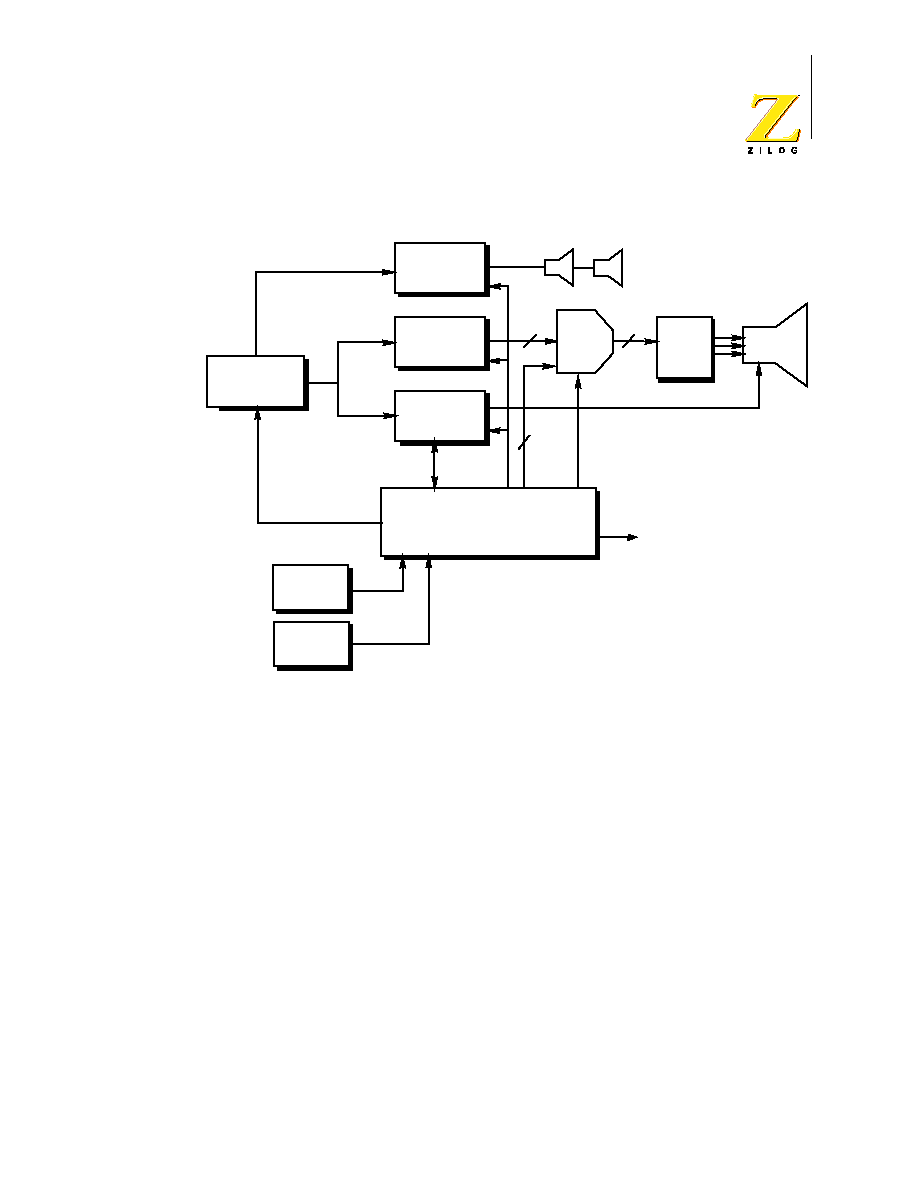
the Z90255. Figure 2 is a block diagram of the Z90255 architecture.
Z90255 ROM and Z90251 OTP
32 KB Television Controller with OSD
PS001301-0800
2
Figure 1
Z90255-Based TV System Application
Audio
Color
Decoder
Deflection
Unit
FM Audio
Tuning
Control
R.G.B.
Composite
Video
Control
R.G.B.
VBLANK
Z90255 Television
OSD Controller
R.G.B.
HSYNC, VSYNC
I
2
C Bus
CRT
RGB
Output
Stages
SYNC
Front Panel
I/R
Detector
MUX
Keypad
IF Demodulator
Television
Tuner
Z90255 ROM and Z90251 OTP
32 KB Television Controller with OSD
PS001301-0800
3
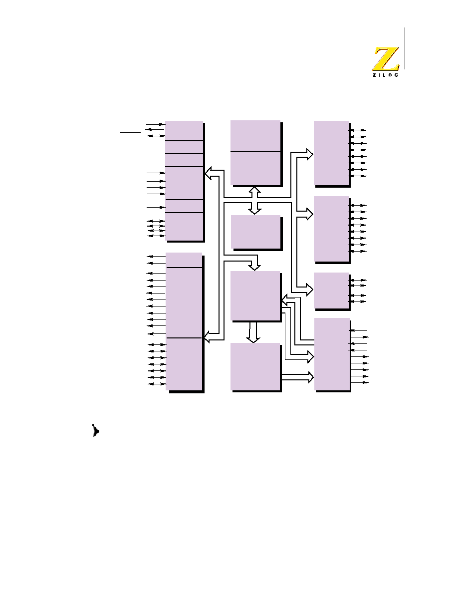
Figure 2
Z90255 Block Diagram
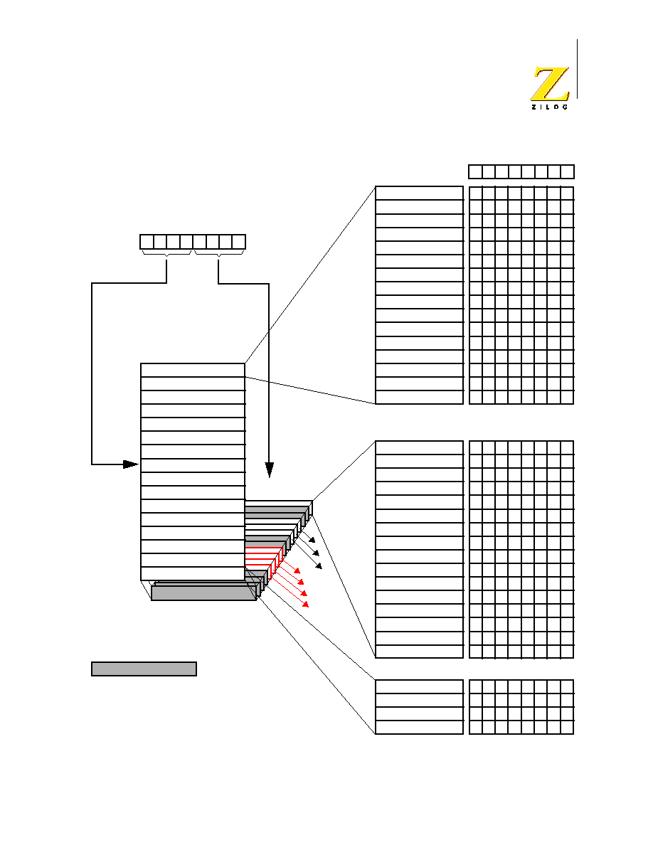
PWM 6 can be either a 6-bit or 14-bit output.
The Z90255 takes full advantage of Zilog’s Z8 expanded register file space to
offer greater flexibility in creating a user-friendly On-Screen Display (OSD).
Three basic addressing spaces are available: Program memory, Video RAM
(VRAM) and the Register file. The register file is composed of 300 bytes of
general-purpose registers, 16 control and status registers, one I/O port register
and three reserved registers.
RESET
Oscillator
WDT
Counter
Timer
Counter
Timer
4-Bit
ADC
IR
Counter
Port 6
300 Byte
Register File
Port 2
18 KB by 7-Bit
Character
PWM 11 & 6
PWM 1
to
PWM 10
(14-bit)
(6-bit)
XTAL1
XTAL2
RESET
ADC0
ADC1
ADC2
ADC3
IRIN
P60
P61
P62
P63
P21
P22
P23
P24
P25
P26
P27
P20
PWM11
PWM1
PWM2
PWM3
PWM4
PWM5
PWM6
PWM8
PWM9
PWM10
SCLK0
SDATA0
I
2
C
P50
P51
P52
P53
P54
P55
P56
Port 5
Interface
SCLK1
SDATA1
ROM or OTP
PWM7
240 x 12-Bit
Character RAM
& 10 x 8-Bit
32 KB
Program ROM
Microprocessor
Core
or
32 KB
Program OTP
Internal
On-Screen
Display
OSDX1
OSDX2
H
SYNC
V
SYNC
R
G
B
V
BLANK
HLFTN
Port 4
P40
P41
P42
P43
P44
P45
P46
P47
PWM6
Note:

Z90255 ROM and Z90251 OTP
32 KB Television Controller with OSD
PS001301-0800
4
The OSD module supports 10 rows by 24 columns of characters. Each character
color can be specified. There are eight foreground colors and eight background
colors. When the foreground and background colors are the same, the
background is transparent.
If Row, Second color and Character set are defined, an analog bar line can be
displayed for volume control, signal levels, and tuning.
The OSD can display four character sizes:
∑
1X (14 x 18 pixels)
∑
2X (28 x 36 pixels)
∑
Double width (28 x 18 pixels)
∑
Double height (14 x36 pixels)
Inter-row spacing can be programmed within 0 to 15 Horizontal scan lines. Using
multiple characters with zero inter-row spacing allows the creation of large psuedo
icons.
A 14-bit Pulse Width Modulator (PWM) port provides necessary voltage resolution
for a voltage synthesizer tuning system. Ten 6-bit PWM ports are used to control
audio (base, treble, balance and volume) and video (contrast, brightness, color,
tint and sharpness) signal levels.
There are 27 I/O pins grouped into four ports. These I/O pins can be configured
through software to provide timing, status signals, serial and parallel input and
output.
For real-time events, such as counting, timing and data communication, two on-
chip counter/timers are implemented. The Z90255 is packaged in a 42-pin SDIP
and provides an ideal, reliable solution for high-volume consumer television
applications.
Z90255 ROM and Z90251 OTP
32 KB Television Controller with OSD
PS001301-0800
5
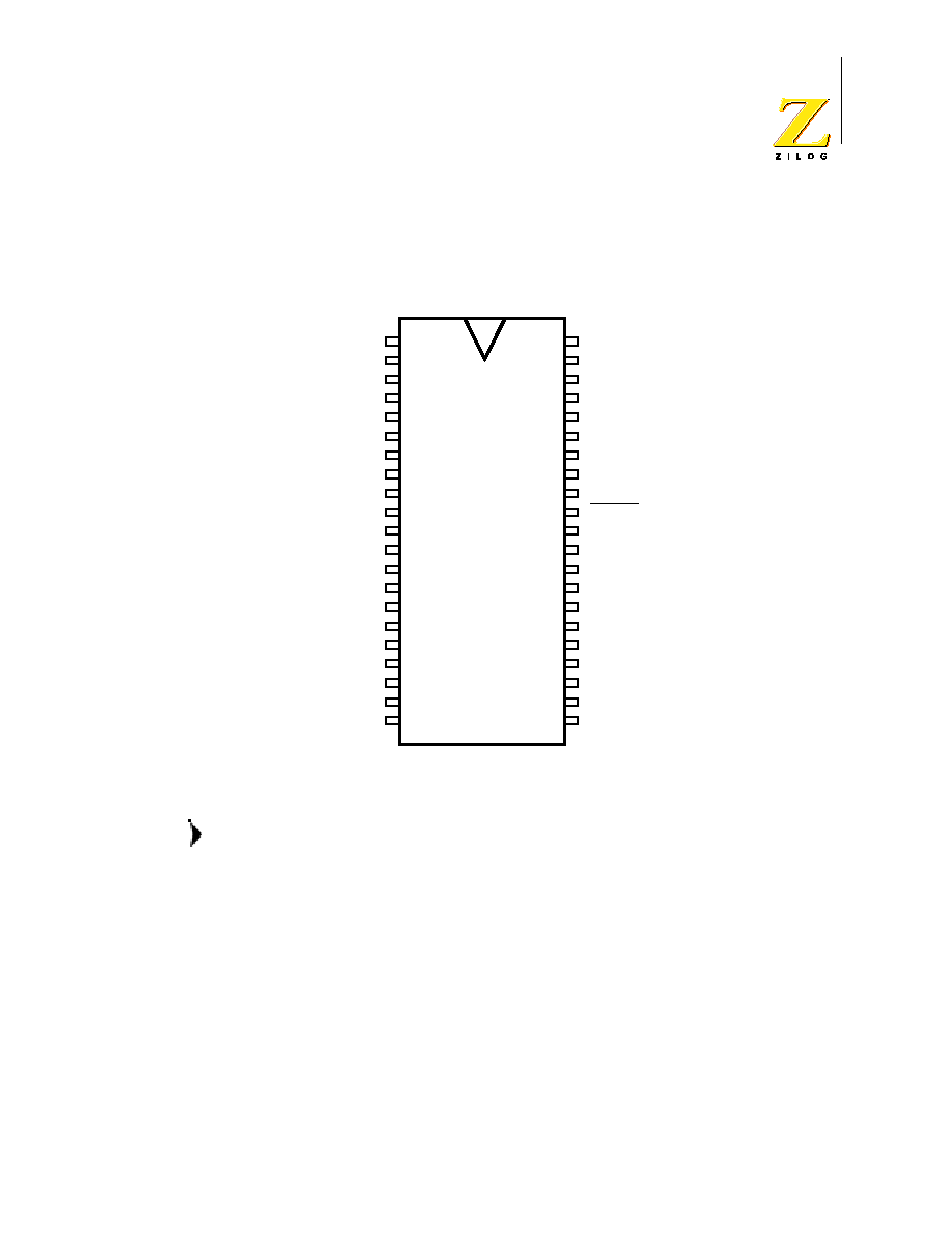
1.1
Pin Assignment and Descriptions
Figure 3 shows the pin numbers for production and OTP device format.
Figure 3
Z90255 and Z90251 Pin Assignments
1
The pins on the Z90255 and Z90251 are assigned to
perform the functions identified in Tables 1, 2 and 3.
2
PWM 6 can be either 6-bit or 14-bit PWM outputs.
3
All signals with an overbar are active Low.
1
2
3
4
5
6
7
8
9
10
11
12
13
14
15
42
41
40
39
38
37
36
35
34
33
32
31
30
29
28
16
17
18
19
20
21
27
26
25
24
23
22
PORT56/PWM11
PORT55/PWM6
PORT54/PWM5
PORT53/PWM4
PORT52/PWM3
PORT51/PWM2
PORT40
PORT61/ADC2
PORT62/ADC0
AGND
PORT42
PORT43
PORT63
PORT44/PWM7
PORT45/PWM8
PORT46/PWM9
PORT20/HLFTN
PORT27/SDATA1
PORT26/SCLK1
PORT25/SDATA0
PORT24/SCLK0
PORT23
PORT
22
IRIN
PORT21
V
CC
RESET
XTAL2
XTAL1
GND
OSDX2
OSDX1
VSYNC
HSYNC
VBLANK
R
G
B
PORT50/PWM10
PORT60/ADC3
PORT41/ADC1
PORT47/PWM10
Z90251
or
Z90255
(Top View)
Notes:

Z90255 ROM and Z90251 OTP
32 KB Television Controller with OSD
PS001301-0800
6
Table 1
Z90255 Production Device Pin Assignment
Name
Pin Function
Package 42-Pin SDIP
Direction POR
V
CC
+5 Volts
34
Power
Power
GND, AGND
0 Volts
30, 13
Power
Power
IRIN
Infrared Remote Capture Input
36
I
I
PWM11
14-bit Pulse Width Modulator Output
1
O
N/A
PWM10-PWM1
1
6-Bit Pulse Width Modulator Output
20, 19, 18, 17, 2, 3, 4, 5, 6, 7 O
N/A
P5 (6-0)
Bit Programmable I/O Ports
1, 2, 3, 4, 5, 6, 7
I/O
I
P2 (7-0)
Bit-Programmable I/O Ports
42, 41, 40, 39, 38, 37, 35, 21 I/O
I
HLFTN
Halftone Output
21
O
N/A
SDATA0, SDATA1
I
2
C Data, Bidirectional (Send/Receive)
Serial Data Lines
40, 42
2
I/O
N/A
SCLK0, SCLK1
I
2
C Clock
39, 41
2
I/O
N/A
P6 (3-0)
Bit-Programmable I/O Ports
16, 12, 10, 9
I/O
I
P4 (7-0)
Bit-Programmable I/O Ports
20, 19, 18, 17, 15, 14, 11, 8
I/O
I
XTAL1
Crystal Oscillator Input
31
I
I
XTAL2
Crystal Oscillator Output
32
O
O
OSDX1
Dot-Clock Oscillator Input
28
I
I
OSDX2
Dot-Clock Oscillator Output
29
O
O
H
SYNC
Horizontal Synchronization
26
I
I
V
SYNC
Vertical Synchronization
27
I
I
VBLANK
Video Blanking
25
O
O
R,G,B
Video Red, Green, Blue
24, 23, 22
O
O
ADC3-ADC0
4-Bit Analog-to-Digital Converter Input
9, 10, 11, 12
AI
I
RESET
System Reset
33
I/O
I
Note: 1 PWM 6 can be either 6-bit or 14-bit PWM outputs.
2 When Pins
39
-
42
are configured for I
2
C, pins
39
and
40
comprise one channel, and pins
41
and
42
comprise another channel

Z90255 ROM and Z90251 OTP
32 KB Television Controller with OSD
PS001301-0800
7
1.2
Single-Purpose Pin Descriptions
Table 2 lists the single-purpose pin acronyms, pin names, and descriptions.
Table 2
Single-Purpose Pin Descriptions
Acronym
Pin Name(s)
Description
AGND
Analog Ground
Analog Ground
B
Blue
CMOS output of the blue video signal B. Video blue can
be programmed for either polarity.
G
Green
CMOS output of the green video signal G. Video green
can be programmed for either polarity.
GND
Ground
Ground
H
SYNC
Horizontal Sync
Input pin for external horizontal synchronization signal
IRIN
IR Capture Input
Infrared Remote capture input
OSDX1, OSDX2 On-Screen Display Dot
Clock Oscillators
These oscillator input and output pins for on-screen
display circuits are connected to an inductor and two
capacitors to generate the character dot clock. The dot
clock frequency determines the character pixel width and
phase synchronized to HSYNC
P21, P22, P23
Port 2 bits 1 - 3
Bidirectional digital port, configured to read digital data or
to send output to an attached device.
P40, P42, P43
Port 4 bit 0, bits 2 and 3
Bidirectional digital port, configured to read digital data or
to send output to an attached device.
P63
Port 6 bit 3
P63 input can be read directly at 03H. A negative edge
event is latched to IRQ3. An IRQ3-vectored interrupt
occurs if appropriately enabled. A typical application
places the device in Stop mode when P63 goes Low
(IRQ3 interrupt routine). When P63 subsequently goes
High, a Stop-Mode Recovery is initiated.
R
Red
CMOS output of the red video signal R. Video red can be
programmed for either polarity.
RESET
System Reset
System reset

Z90255 ROM and Z90251 OTP
32 KB Television Controller with OSD
PS001301-0800
8
1.3
Multiplexed Pin Descriptions
Table 3 lists the Multiplexed Pin acronyms, pin names, and descriptions.
V
BLANK
Video Blank
CMOS output, programmable polarity. This pin is used as
a super-impose control port to display characters from
video RAM. The signal controls Y-signal output of CRTs
and turns off the incoming video display while the
characters in video RAM are super-imposed on the
screen. The output ports of color data directly drive three
electron guns on the CRT; at the same time VBLANK
output turns off the Y signal.
V
CC
Power Supply
Power supply
V
SYNC
Vertical Sync
Input pin for external vertical synchronization signal.
XTAL1, XTAL2
Time-Based
Input
Output
These pins connect to the internal parallel-resonant clock
crystal oscillator circuit with two capacitors to GND.
XTAL1 can be used as an external clock input.
Table 3
Multiplexed Pin Descriptions
Acronym
Pin Name(s)
Description
P20/HLFTN
Port 2 bit 0 or Halftone Output Port 2 bit 0 can be programmed as an input or output
line.
P24/SCLK0
Port 2 bit 4 or
I
2
C Clock
Port 2 bit 4 or
I
2
C Clock
P25/SDATA0
Port 2 bit 5 or
I
2
C Data
Port 2 bit 5 or
I
2
C Data
P26/SCLK1
P27/SDATA1
Port 2 bit 6 or
I
2
C Clock
Port 2 bit 7 or
I
2
C Data
Port 2 bit 6 or
I
2
C Clock
Port 2 bit 7 or
I
2
C Data
P62/ADC0
Port 6 bit 2 or
Analog-to-Digital Converter
Channel 0
P62 can be read directly. A negative edge event is
latched into IRQ2 to initiate an IRQ2-vectored interrupt if
appropriately enabled.
P60/ADC3
Port 6 bit 0 or
Analog-to-Digital Converter
Channel 3
Port 6 bit 0 can be programmed as an input or output
line.
Table 2
Single-Purpose Pin Descriptions (Continued)
Acronym
Pin Name(s)
Description

Z90255 ROM and Z90251 OTP
32 KB Television Controller with OSD
PS001301-0800
9
P61/ADC2
Port 6 bit 1 or
Analog-to-Digital Converter
Channel 2
Port 6 bit 1 can be programmed as an input or output
line.
P41/ADC1
Port 4 bit 1 or
Analog-to-Digital Converter
Channel 1
Port 4 bit1 can be programmed as an input or output
line.
P44/PWM7
P45/PWM8
P46/PWM9
P47/PWM10
Port 4 bit 4 or Pulse Width
Modulator 7
Port 4 bit 5 or Pulse Width
Modulator 8
Port 4 bit 6 or Pulse Width
Modulator 9
Port 4 bit 7 or Pulse Width
Modulator 10
These port pins can be programmed as input or output
ports. Each PWM channel has 6-bit resolution.
PWM11/P56
PWM6/P55
Pulse Width Modulator 11 or
Port 5 bit 6
Pulse Width Modulator 6 or
Port 5 bit 5
The PWM signal-generator channel has 14-bit
resolution. Port 5 bit 6 and port 5 bit 5 can be
programmed as inputs or outputs.
PWM6/P55
PWM5/P54
PWM4/P53
PWM3/P52
Pulse Width Modulator 6 or
Port 5 bit 5
Pulse Width Modulator 5 or
Port 5 bit 4
Pulse Width Modulator 4 or
Port 5 bit 3
Pulse Width Modulator 3 or
Port 5 bit 2
These port pins can be programmed as input or output
ports. Each PWM signal-generator channel has 6-bit
resolution.
PWM2/P51
Pulse Width Modulator 2 or
Port 5 bit 1
The PWM signal-generator channel has 6-bit resolution.
Port 5 bit 1 and Port 5 bit 0 can be programmed as an
input or output port.
PWM1/P50
Pulse Width Modulator 1 or
Port 5 bit 0
The PWM signal-generator channel has 6-bit resolution.
Port 5 bit 0 can be programmed as an input or output
port.
Note: PWM6 can be either 6-bit or 14-bit output.
Table 3
Multiplexed Pin Descriptions (Continued)
Acronym
Pin Name(s)
Description
Z90255 ROM and Z90251 OTP
32 KB Television Controller with OSD
PS001301-0800
10
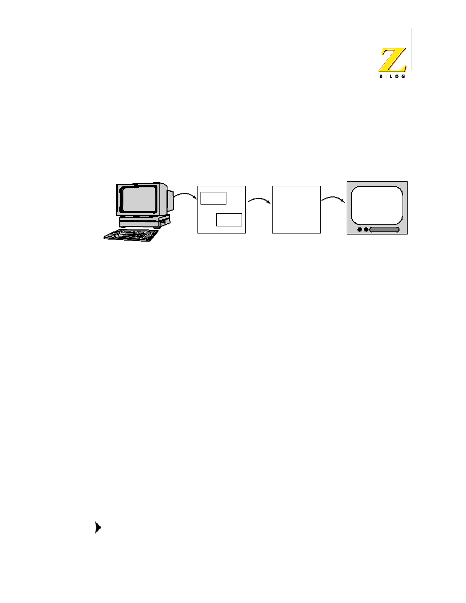
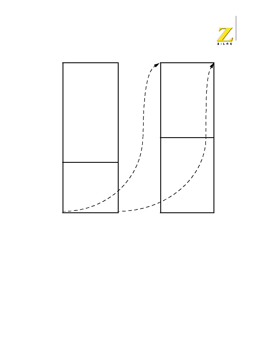
The Z90251 requires Zilog’s Z90259ZEM Emulator with its proprietary Zilog
Developmental Studio (ZDS) software for programming. To view how code
is working, the emulator uses a ZOSD board which connects directly to a
television screen. Refer to Figure 4.
Figure 4
Code Development Environment
2
Memory Description
A total of 300 bytes of general purpose register memory is implemented in the
Z90255. These registers are composed of 236 registers from the standard
register file and 64 registers from the expanded register file.
2.1
Standard Register File
The Z90255 Standard Register File consists of two I/O port registers (02h and
03h), 236 general purpose registers (04h-EFh) and 15 (F1h-FFh) control and
status registers. Registers 00h, 01h, and F0h are reserved. Figure 5 is the
register file map. Instructions can access registers directly or indirectly with an 8-
bit address field. This also allows short 4-bit addressing using the Register
Pointer. In the 4-bit mode, the register file is divided into sixteen working register
groups. The upper nibble of the Register Pointer (FDh) addresses the starting
location of the active working-register group.
Registers E0h-EFh are only accessed through a working-
register and indirect addressing mode.
Develop
code on PC
Z90259
Z90251
Z90259 In-Circuit
Emulator (ICEbox)
ZOSD Board
Converts to
Video Display
Download Code to
Z90259 ICE chip
Program the
Z90251 OTP
Review Code
on TV Display
Note:

Z90255 ROM and Z90251 OTP
32 KB Television Controller with OSD
PS001301-0800
11
2.2
Expanded Register File
The register file has been expanded to provide additional system control registers,
additional general purpose registers, and expanded mapping of peripheral
devices and I/O ports in the register address area.
The lower nibble of the Register Pointer (FDh) addresses the Expanded Register
File (ERF) Bank. The 0h value in the lower nibble identifies the Standard Register
File to be addressed. Any other value from 1h to Fh selects an ERF Bank. When
an ERF Bank is selected, register addresses from 00h to 0Fh access the sixteen
ERF Bank registers, which in effect replace the first sixteen locations of the
Z90255 Standard Register File. Only ERF Bank 4, ERF Bank 5, ERF Bank 6, ERF
Bank 7, ERF Bank A, ERF Bank B, ERF Bank C and ERF Bank F are
implemented in the Z90255 controller (Table 4).
2.3
Program Memory
The Z90255 has 32KB of program memory. Refer to Figure 6. The first 12 bytes of
the program memory are reserved for the interrupt vectors. These locations
contain six 16-bit vectors that correspond to interrupt and program control routine
addresses which are passed to the specified vector address. The IRQ0 vector is
permanently assigned to the IR interrupt request. The IRQ1 vector is permanently
assigned to the V
SYNC
and H
SYNC
interrupt request. Program memory starts at
address 000Ch after being reset.
Z90255 ROM and Z90251 OTP
32 KB Television Controller with OSD
PS001301-0800
12
Figure 5
Register File Map
%00
%0F
%7F
%F0
%FF
%FF SPL
0
0
0
0
0
0
0
0
x
x
x
x
x
x
x
x
0
0
0
0
0
0
0
0
x
x
x
x
x
x
x
x
x
x
x
x
x
x
x
x
0
x
x
x
x
x
x
x
1
1
1
1
1
1
1
1
0
0
0
0
0
0
0
1
1
1
1
1
1
1
1
1
x
x
x
x
x
x
x
0
x
x
x
x
x
x
x
x
x
x
x
x
x
x
0
0
x
x
x
x
x
x
x
x
0
0
0
0
0
0
0
0
x
x
x
x
x
x
x
x
%FE SPH
%FD RP
%FC FLAGS
%FB IMR
%FA IRQ
%F9 IPR
%F8 P01M
%F7 P2CNTL
%F6 P2M
%F5 PRE0
%F4 T0
%F3 PRE1
%F2 T1
%F1 TMR
%F0 Reserved
D7 D6 D5 D4 D3 D2 D1
D0
x
x
x
x
x
1
x
x
0
0
1
0
0
0
0
0
1
1
1
1
1
1
1
0
%(F)0F WDTMR
%(F)0E Reserved
%(F)0D Reserved
%(F)0C Reserved
%(F)0B SMR
%(F)0A Reserved
%(F)09 PWM6H
%(F)08 PWM6L
%(F)07 MC_Reg
%(F)06 MR_En
%(F)05 MC_End
%(F)04 MC_St
%(F)03 PRT6_DTA
%(F)02 PRT6_DRT
%(F)01 4ADC_DTA
%(F)00 PCON
%(0)03 Reserved
%(0)02 P2
%(0)01 Reserved
%(0)00 Reserved
D7 D6 D5 D4 D3 D2 D1 D0
Expanded Register
Bank Pointer
Working Register
Group Pointer
Z8 Register File
Reset Condition
Register
Expanded Register Bank (F)
Register
Reset Condition
Register
Reset Condition
Reserved Expanded
Register
x
x
x
x
x
x
x
x
x
x
x
0
0
0
0
0
x
x
x
0
0
0
0
0
0
0
0
0
0
0
0
0
0
0
0
0
0
0
0
0
(7)
(B)
(C)
Register Pointer
0
0
0
0
x
x
x
x
1
1
1
1
1
1
1
1
1
1
1
1
1
1
1
1
(4)
(5)
(6)
(A)
0
0
0
0
0
0
0
0
x
x
0
0
0
0
0
0
x = undefined
Z90255 ROM and Z90251 OTP
32 KB Television Controller with OSD
PS001301-0800
13
Table 4
Register File Map
BANK 4
BANK 5
BANK 6
BANK 7
Address Description
Address Description
Address
Description Address Description
00h-0Fh Gen. Pur. Reg.
00h-0Fh Gen. Pur. Reg.
00h-0Fh
Gen. Pur. Reg. 00h-0Fh Gen. Pur. Reg.
BANK A
BANK B
Address Description
Address Description
00h
OSD Control Register(OSD_CNTL)
00h
PWM11-High Data Register(PWM11H)
01h
Vertical Position Register(VERT_POS)
01h
PWM11-Low Data Register(PWM11L)
02h
Horizontal Position Register(HOR_POS)
02h
PWM1 Data Register(PWM1)
03h
Display Attribute Register(DISP_ATTR)
03h
PWM2 Data Register(PWM2)
04h
Row Space Register (ROW_SPACE)
04h
PWM3 Data Register(PWM3)
05h
Fade Position1 Register(FADE_POS1)
05h
PWM4 Data Register(PWM4)
06h
Fade Position2 Regisiter(FADE_POS2)
06h
PWM5 Data Register(PWM5)
07h
Second Color Control
Register(SNDCLR_CNTRL)
07h
PWM6(6-bit) Data Register(PWM6_6)
08h
Second Color Position
Register(SNDCLR_POS)
08h
PWM7 Data Register(PWM7)
09h
Color Palette0 Register(CLR_P0)
09h
PWM8 Data Register(PWM8)
0Ah
Color Palette1 Register(CLR_P1)
0Ah
PWM9 Data Register(PWM9)
0Bh
Color Palette2 Register(CLR_P2)
0Bh
PWM10 Data Register(PWM10)
0Ch
Color Palette3 Register(CLR_P3)
0Ch
Port 5 Data Register(PRT5_DTA)
0Dh
Color Palette4 Register(CLR_P4)
0Dh
PWM Mode Register(P_MODE)
0Eh
Color Palette5 Register(CLR_P5)
0Eh
Port 5 Direction Register(PRT5_DRT)
0Fh
Color Palette6 Register(CLR_P6)
0Fh
BANK C
BANK F
Address Description
Address Description
00h
3-bit ADC Data Register(3ADC_DTA)
00h
Port Configuration Register(PCON)
01h
Timer Control Register0(TCR0)
01h
4-bit ADC Data Register (4ADC_DTA)
02h
Timer Control Register1(TCR1)
02h
Port6 Direction Register(PRT6_DRT)
03h
IR Capture Register0(IR_CP0)
03h
Port6 Data Register (PRT6_DTA)
04h
IR Capture Register1(IR_CP1)
04h
Mesh Column Start Register(MC_ST)
05h
Port4 Data Register(PRT4_DTA)
05h
Mesh Column End Register(MC_END)
06h
Port4 Direction Register(PRT4_DRT)
06h
Mesh Row Enable Register(MR_EN)
07h
Interrupt Status Register(INT_ST)
07h
Mesh Control Register(MC_REG)
08h
Port4 Pin_out Selection Register(PIN_SLT)
08h
PWM6 High Data Register(PWM6H_14)
09h
Color Index Register(CLR_IDX)
09h
PWM6 Low Data Register (PWM6L_14)
0Ah
I2C Data Register(I
2
C_DATA)
0Ah
0Bh
I2C Command Register(I
2
C_CMD)
0Bh
Stop Mode Register(SMR)
0Ch
I2C Control Register(I
2
C_CNTL)
0Ch
0Dh
0Dh
0Eh
0Eh
0Fh
0Fh
WDT Mode Register(WDTMR)
Z90255 ROM and Z90251 OTP
32 KB Television Controller with OSD
PS001301-0800
14
Figure 6
Program Memory Map
IR IRQ0(High Byte)
0000h
Reserved
8000h
IR IRQ0(Low Byte)
0001h
HVSYNC IRQ1(High Byte)
0002h
HVSYNC IRQ1(Low Byte)
0003h
P62 IRQ2(High Byte)
0004h
P62 IRQ2(Low Byte)
0005h
P63 IRQ3(High Byte)
0006h
P63 IRQ3(Low Byte)
0007h
T0 IRQ4(High Byte)
0008h
FBFFh
T0 IRQ4(Low Byte)
0009h
Video
Refresh
RAM
FC00h
T1 IRQ5(High Byte)
000Ah
T1 IRQ5(Low Byte)
000Bh
Reset Start Address
On Chip Program Space
(32KB)
000Ch
7FFFh
FFFFh

Z90255 ROM and Z90251 OTP
32 KB Television Controller with OSD
PS001301-0800
15
3
Watch-Dog Timer (WDT)
The Watch-Dog Timer (WDT) is driven by an internal RC oscillator. Therefore
accuracy is dependent on the tolerance of the RC components. Table 5 describes
the Watch-Dog Timer Mode register bits.
WDT During Halt Mode (T2)
Bit 2 determines if the WDT is active during Halt Mode. A
1
value indicates active
during Halt. The default is 1. A WDT timeout during Halt Mode resets control
registers and ports to their default reset conditions.
Bit 3 determines if the WDT is active during Stop mode. A
1
value indicates
active during Stop mode. A WDT timeout during Stop mode resets control
registers and ports to their default reset conditions.
Bits 4, 5, 6 and 7 are reserved and must be cleared to
0
.
The WDTMR register is accessible only during the first 60 processor cycles from
the execution of the first instruction after Power-On Reset, Watch-Dog Reset, or a
Table 5
Watch-Dog Timer Mode Register 0Fh: Bank F
Bit
7
6
5
4
3
2
1
0
R/W
W
W
W
W
W
W
W
W
Reset
0
0
0
0
0
1
0
1
Note: R = Read W = Write X = Indeterminate
Bit/
Field
Bit
Position
R/W
Value Description
reserved
7-4
W
0
Must be 0
WDT During Stop
3
W
0
1
Off
On POR
WDT During Halt
2
W
0
1
Off
On POR
WDT TAP
1, 0
W
00
01
10
11
6 msec
12 msec POR
24 msec
96 msec

Z90255 ROM and Z90251 OTP
32 KB Television Controller with OSD
PS001301-0800
16
Stop-Mode Recovery. After this point, the register cannot be modified by any
means, intentional or otherwise.
The WDT is permanently enabled after Reset. To ensure that the WDT is set
properly, use the following instructions as the first two instructions:
DI
WDT
The Watch-Dog timer must then be constantly refreshed within the required
timeout by executing the WDT Instruction.
Executing the WDT instruction affects the Z (zero), S (sign),
and V (overflow) flags.
A system reset overrides all other operating conditions and puts the micro-
controller into a known state. To initialize the chip’s internal logic, the Reset input
must be held Low for at least 5 XTAL clock cycles. The control registers and ports
are reset to default conditions after a POR, a reset from the Reset pin, or a WDT
timeout while in Run Mode and Halt Mode. The control registers and ports are not
reset to their default conditions after Stop Mode Recovery and WDT timeout while
in Stop Mode.
The program counter is loaded with 000Ch. I/O ports and control registers are
configured to their default reset states.
Resetting the microcontroller does not Affect the contents of the general-purpose
registers.
The Watch-Dog Timer (WDT) is a retriggerable, one-shot timer that resets the
microcontroller if it reaches its terminal count. When operating in the Run, Halt or
Stop Modes, a WDT reset is functionally equivalent to a hardware POR reset.
4
Stop Mode and Halt Mode Operation
4.1
Power-Down Halt-Mode Operation
The Halt Mode suspends instruction execution and turns off the internal CPU
clock. The on-chip oscillator circuit remains active so the internal clock continues
to run and is applied to the counter/timer(s) and interrupt logic.
To enter the Halt Mode, the instruction pipeline must be flushed first to avoid
suspending execution in mid-instruction. To do this, the application program must
Note:

Z90255 ROM and Z90251 OTP
32 KB Television Controller with OSD
PS001301-0800
17
execute a NOP instruction (opcode = FFh) immediately before the Halt instruction
(opcode 7Fh), that is,
The Halt Mode is exited by interrupts, generated either externally or internally.
When the interrupt service routine is completed, the user program continues from
the instruction after Halt.
The Halt Mode can also be exited via a POR/Reset activation or a Watch-Dog
Timer (WDT) timeout. In this case, program execution restarts at the reset-restart
address 000Ch.
To reduce power consumption further in the Halt Mode, the Z90255 and Z90251
allow dynamic internal clock scaling. Clock scaling can be accomplished on the fly
by reprogramming bit 0 and/or bit 1 of the Stop-Mode Recovery register (SMR).
Internal clock scaling directly effects Counter/Timer operation:
adjustment of the prescaler and downcounter values might be
required.
4.2
Stop Mode Operation
The Stop Mode provides the lowest possible device standby current. This
instruction turns off the on-chip oscillator and internal system clock.
To enter the Stop Mode, the instruction pipeline must be flushed first to avoid
suspending execution in mid-instruction. To do this, the application program must
execute a NOP instruction (opcode=FFh) immediately before the Stop instruction
(opcode=6Fh), that is,
The Stop Mode is exited by any one of the following resets: Power-On Reset
activation, WDT timeout, or a Stop-Mode Recovery source. When reset is
generated, the processor always restarts the application program at address
000Ch.
POR/Reset activation is present on the Z90255 and Z90251 and is implemented
as a reset pin and/or an on-chip power on reset circuit.
When the WDT is configured to run during Stop mode, the WDT timeout
generates a Reset ending Stop Mode.
FF
NOP
;clear the instruction pipeline
7F
Halt
;enter Halt Mode
FF
NOP
;clear the instruction pipeline
6F
Stop
;enter Stop Mode
Note:

Z90255 ROM and Z90251 OTP
32 KB Television Controller with OSD
PS001301-0800
18
Stop-Mode Recovery (SMR) by the WDT increases the Stop
Mode standby current (ICC2). This is because the internal RC
oscillator is running to support this recovery mode.
The Z90255 and Z90251 have Stop-Mode Recovery (SMR) circuitry. Two SMR
methods are implemented, a single-fixed input pin or a flexible, programmable set
of inputs. The Z8-base product specification should be reviewed to determine the
SMR options available.
In simple cases, a Low level applied to input pin P27 triggers an SMR. To use this
mode, pin P27 (I/O Port 2, bit 7) must be configured as an input before entering
Stop Mode. The Low level on P27 must meet a minimum pulse width TWSM.
Some microcontrollers provide multiple SMR input sources. The SMR source is
selected via the SMR Register.
Using specialized SMR modes (P27 input or SMR register
based) or the WDT timeout (only when in the Stop Mode)
provides a unique reset operation. Some control registers are
initialized differently for a SMR/WDT triggered POR than a
standard reset operation.
The Stop Mode current (ICC2) is minimized when
- V
CC
is at the low end of the device operating range
- WDT is Off in Stop Mode
- Output current sourcing is minimized
- All inputs (digital and analog) are at the low or high rail voltages
4.3
STOP Mode Recovery Register
The STOP Mode Recovery Register register selects the clock divide value and
determines the mode of Stop Mode Recovery. All bits are Write-Only, except bit 7
which is Read-Only. Bit 7 is a flag bit that is hardware set in a Stop Mode
Recovery condition, and reset by a power-on cycle. Bit 6 controls whether a Low
level or a High level is required from the recovery source. Bit 5 controls the reset
delay after recovery. Bits 2, 3, and 4, of the SMR register, specify the source of the
Stop-Mode Recovery signal. Bits 0 and 1 control internal clock divider circuitry.
The SMR is located in bank F of the expanded register file at address 0Bh.
Table 6 contains Stop Mode Recovery (SMR) Register bit descriptions.
Note:
Note:
Note:

Z90255 ROM and Z90251 OTP
32 KB Television Controller with OSD
PS001301-0800
19
Table 6
Stop Mode Recovery (SMR) Register 0Bh: Bank F (SMR)
Bit
7
6
5
4
3
2
1
0
R/W
R
W
W
W
W
W
W
W
Reset
0
0
1
0
0
0
0
0
Note: R = Read W = Write X = Indeterminate
Bit/
Field
Bit
Position
R/W
Value Description
Stop flag
7
R
0
1
POR
Stop Recovery
Stop Recovery level
6
W
0
1
Low POR
High
Stop Delay
5
W
0
1
Off
On POR
Stop Mode Recover
Source
4-2
W
000
001
010
011
100
101
110
111
POR and /or External Reset
P63
P62
Must NOT be used
Must NOT be used
P27
P2 NOR 0-3
P2 NOR 0-7
External Clock Divide by 2
1
W
0
1
SCLK/TCLK = XTAL/2 POR
SCLK/TCLK = XTAL
SCLK/TCLK Divide by 16
0
W
0
1
Off POR
On
SCLK/TCLK Divide-by-16
Select (bit O)
This bit controls a divide-by-16 prescaler of
SCLK/TCLK. The purpose of this control is to
reduce device power consumption selectively
during normal processor execution (SCLK
control) and/or Halt Mode (where TCLK
sources counter/timers and interrupt logic).

Z90255 ROM and Z90251 OTP
32 KB Television Controller with OSD
PS001301-0800
20
Figure 7 illustrates Stop Mode Recovers Source/Level Select.
External Clock Divide-by-Two
(bit 1)
This bit can eliminate the oscillator divide-by-
two circuitry. When this bit is 0, the System
Clock (SCLK) and Timer Clock (TCLK) are
equal to the external clock frequency divided by
two. The SCLK/TCLK is equal to the external
clock frequency when this bit is set (D1=1).
Using this bit together with D7 of PCON helps
lower EMI (D7 (PCON) =0, D1 (SMR) =1). The
default setting is zero.
Stop-Mode Recovery Source
(bits 2, 3, and 4)
These three bits specify the wake-up source of
the Stop-Mode recovery.
Table 7
Stop Mode Recovery Source
Bits
Operation
4
3
2
Description of Action
0
0
0
POR and/or external reset recovery
0
0
1
P63 transition
0
1
0
P62 transition (not in Analog Mode)
1
0
1
P27 transition
1
1
0
Logical NOR of P20 through P23
1
1
1
Logical NOR of P20 through P27
Stop Mode Recovery Delay
Select (bit 5)
This bit, if High, enables the T
POR
Reset delay
after Stop Mode Recovery. The default
configuration of this bit is
1
. If the fast wake up
is selected, the Stop Mode Recovery source is
kept active for at least 5 TpC.
Z90255 ROM and Z90251 OTP
32 KB Television Controller with OSD
PS001301-0800
21
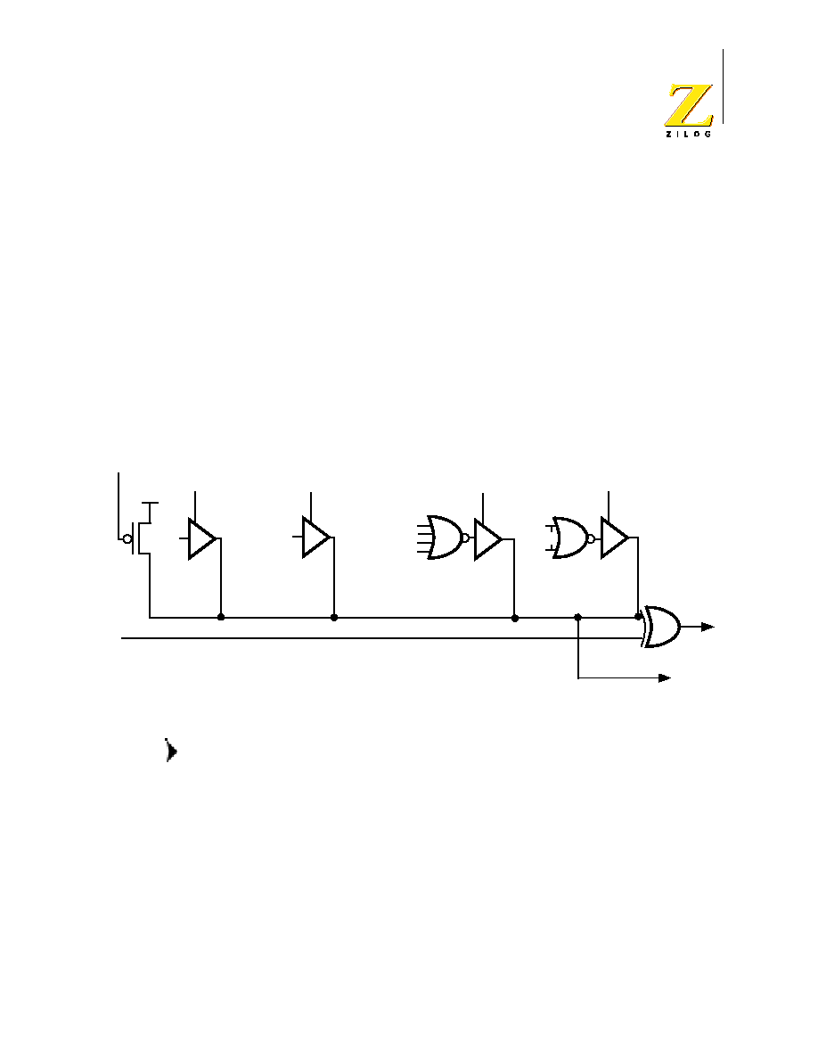
Figure 7
Stop Mode Recovery Source/Level Select
If P62 is used as an SMR source, the digital mode of operation
must be selected before entering Stop Mode.
Stop Mode Recovery Level
Select (bit 6)
A
1
in this bit position indicates that a High level
on any one of the recovery sources wakes the
microcontroller from Stop Mode. A 0 indicates
Low-level recovery. The default is
0
on POR.
Cold or Warm Start (bit 7)
This bit is set by the device when Stop Mode is
entered. A
0
in this bit (cold) indicates that the
device reset by POR/WDT Reset. A
1
in this bit
(warm) indicates that the device awakens by a
SMR source.
SMR D4 D3 D2
0 0 0
SMR
D4 D3 D2
0 0 1
0 1 0
SMR D4 D3 D2
1 0 1
SMR D4 D3 D2
1 1 0
SMR D4 D3 D2
1 1 1
VDD
P20
P23
P20
P27
P63
P27
P62
Stop-Mode Recovery Edge
Select (SMR)
To IRQ1
To POR
Reset
Note:

Z90255 ROM and Z90251 OTP
32 KB Television Controller with OSD
PS001301-0800
22
5
On-Screen Display
The On-Screen Display (
OSD
) module generates and displays a 10 row by 24
columns of 512 characters at 14 x 18-dots resolution. The color of each character
can be specified independently.
The televison OSD controller uses
H
SYNC
and V
SYNC
signals to synchronize its
internal circuitry to the video signal, then outputs RGB and Video Blank (
VBLANK
)
signals. The
VBLANK
signal is used to multiplex the OSD signal and video signal
onto the screen. The result is that the On-Screen Display is superimposed over
the TV picture.
The display results from the successful timing of several components:
∑
OSD Positioning
∑
Second Color Feature
∑
Mesh and Halftone Effect
∑
OSD Fade
∑
Inter-Row Spacing
∑
Character Generation
5.1
OSD Position
OSD Positioning is controlled by programming the following registers:
∑
OSD Control Register (Table 8)
∑
Vertical Position Register (Table 9)
∑
Horizontal Position Register (Table 10)
OSD Control Register
Table 8
OSD Control Register 00h:Bank A (OSD_CNTL)
Bit
7
6
5
4
3
2
1
0
R/W
R/W
R/W
R/W
R/W
R/W
R/W
R/W
R/W
Reset
0
x
x
x
x
x
x
x
Note: R = Read W = Write X = Indeterminate

Z90255 ROM and Z90251 OTP
32 KB Television Controller with OSD
PS001301-0800
23
Bit
4
, Sync Polarity, provides the polarity of the
H
SYNC
and
V
SYNC
signals.
H
SYNC
and
V
SYNC
must have the same polarity (see Figure 8). This feature is designed to
provide flexibility for TV chassis designers.
Figure 8
Positive and Negative Sync Signals
Bit
3
, Character Size, sets the size of the characters that are displayed. Character
sizes 1X, 2X, double width and double height are supported. The default value is
1X
.
To change the size of the characters in a row, alter the value of the bit during the
previous horizontal interrupt. The character size of the first row is programmed
during vertical interrupt (
V
SYNC
) processing. Character size is a row attribute.
Bits
2
,
1
, and
0
, Vertical Retrace Blanking, set a time period when the
OSD
is
disabled while the electron gun returns from the bottom to the top of the screen,
and all
VBLANK
and RGB output are disabled. The blanking period is determined
by counting horizontal pulses according to the following formula:
Blanking Period=(4 x (Vertical Retrace Blanking)+2) x THL
THL:
one horizontal period
The retrace blanking bits,
OSD_CNTL (2,1,0)
must be set to deactivate the
electron guns during the retrace period.
Bit/
Field
Bit
Position R/W
Value Description
OSD Blank
7
R/W
0
1
Enable OSD - POR default
Disable OSD
VRAM Mode
6, 5
R/W
00
01
10
11
Select 10-row buffer mode
Reserved
Select 2-row buffer mode
Reserved
Sync Polarity
4
R/W
0
1
Positive
Negative
Character Size
3
R/W
0
1
1X
2X
Vertical Retrace Blanking
2, 1, 0
R/W
Retrace Blanking
Positive SYNC
Negative SYNC

Z90255 ROM and Z90251 OTP
32 KB Television Controller with OSD
PS001301-0800
24
Vertical Position Register
The Vertical Position Register (Table 6) sets the vertical placement of the
OSD
on
the screen. The unit of measure for placement is the number of scan lines from
the top of the TV field.
The value required for this register can be computed using the following equation:
VERT_POS = (V
POS
- 6) / 4
VERT_POS
represents the contents of bits 5,4,3,2,1,0 of the Vertical Position
Register (
VERT_POS
). The default value is
0
. When the value is
0
, the OSD is at
the top-most OSD position on the screen, with an offset of
06h
scan lines above
the OSD area.
VERT_POS
is the number of scan lines from the V
SYNC
to the OSD start position.
V
POS
must be a positive integer with a minimum value of Ah incrementing by 4.
Table 9
Vertical Position Register 01h:Bank A (VERT_POS)
Bit
7
6
5
4
3
2
1
0
R/W
R/W
R/W
R/W
R/W
R/W
R/W
R/W
R/W
Reset
0
0
0
0
0
0
0
0
Note: R = Read W = Write X = Indeterminate
Bit/
Field
Bit
Position
R/W
Value Description
reserved
7
R
W
0
1
Return 0
No effect
Character double
height
6
R/W
0
1
Normal when bit 3 of OSD_CNTL is
0
.
2X when bit 3 of OSD_CNTL is
1
.
Double height when bit 3 of OSD_CNTL
is
0.
Double width when bit 3 of OSD_CNTL
is
1
.
Vertical Position
5,4,3,2,1,0
R/W
Vertical position control

Z90255 ROM and Z90251 OTP
32 KB Television Controller with OSD
PS001301-0800
25
Horizontal Position Register
The Horizontal Position Register sets the horizontal start position of the
OSD
(Table 7). The unit of measure for placement is the number of pixels from the left
of the display screen.
When working with Progressive mode, fringing does not work
with 2X mode or double height mode, nor does Mesh work the
same way as in Interlace mode.
The value required for this register can be computed using the following equation:
HOR_POS = (H
POS
- 1) / 4
HOR_POS
represents the contents of bits
5,4,3,2,1,0
of the Horizontal
Position Register (
HOR_POS
). The default value is
3h
. When the value is
3h
, the
OSD is at the left-most OSD position on the screen.
H
POS
is the number of pixels from the left of the screen to the OSD start position.
H
POS
must be a positive integer with a minimum value of
5
incrementing by
4
.
5.2
Second Color Feature
Second Color feature is the logical division of each column into two parts along
each row for changing foreground color. The number of each half-column is called
the Second Color Position.
Table 10 Horizontal Position Register 02h:Bank A (HOR_POS)
Bit
7
6
5
4
3
2
1
0
R/W
R/W
R/W
R/W
R/W
R/W
R/W
R/W
R/W
Reset
0
1
0
0
0
0
1
1
Note: R = Read W = Write X = Indeterminate
Register Field
Bit Position R/W
Data
Description
Progressive mode
7-------
R/W
0
1
Normal
Support progressive sync inputs
Reserved
-6------
R
W
Return 1
No effect
Horizontal position
5,4,3,2,1,0
R/W
Horizontal position control

Z90255 ROM and Z90251 OTP
32 KB Television Controller with OSD
PS001301-0800
26
The Second Color feature can be used to implement an analog bar for volume
control, tuning, etc. The change step for color is half the character size. Refer to
Tables 8 and 9.
Second Color Control Register
The Second Color Position is the place where the foreground color changes to the
color defined in the Second Color Control Register.
Second Color Register
Table 11 Second Color Control Register 07h:Bank A (SNDCLR_CNTRL)
Bit
7
6
5
4
3
2
1
0
R/W
R/W
R/W
R/W
R/W
R/W
R/W
R/W
R/W
Reset
0
0
0
0
0
0
0
0
Note: R = Read W = Write X = Indeterminate
Bit/
Field
Bit
Position R/W
Value Description
Second Color Enable
7
R/W
0
1
Disables the second color feature
Enables the second color feature
Second Color
6, 5, 4
R/W
R, G, B respectively. Defines the
second color after the second color
position defined in SNDCLR register.
Row Address
3, 2, 1, 0
R/W
Defines one of the 10 rows (from 0, the
first row, to 9, the 10th row).
Table 12 Second Color Register 08h:Bank A (SNDCLR)
Bit
7
6
5
4
3
2
1
0
R/W
R/W
R/W
R/W
R/W
R/W
R/W
R/W
R/W
Reset
x
0
0
0
0
0
0
0
Note: R = Read W = Write X = Indeterminate

Z90255 ROM and Z90251 OTP
32 KB Television Controller with OSD
PS001301-0800
27
Column increment is 0.5. Offset is
03h
. System software
requires that the offset be added to the increment for the
second color in the bar display. The bar position must be
defined before the second color is enabled.
Bit
6, HV
SYNC
Interrupt Option, defines the procedure for processing when a
second interrupt is issued before the first interrupt has completed processing. If
bit 6 is set to 0, bit 6 is not pending the other interrupt (H
SYNC
or V
SYNC
) while
one is in service. If bit 6 is set to
1
, bit 6 is pending the other interrupt (H
SYNC
or
V
SYNC
) while one is in service.
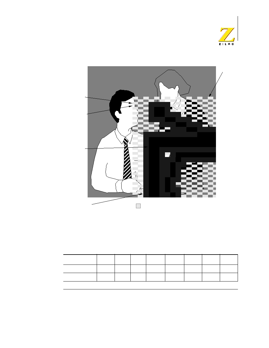
Figures 9 is an example of second color display in the eighth row of the OSD.
Each of the small grid squares represents one pixel. Each column has two areas
for second color display. In this example, the second color is at Position 6. The
second color position for the first column has a value of 3 because the OSD is
offset from the left of the TV screen at a distance equal to 03h. Each column is
the size of one display character. Each Second color column is a half character
column. The screen position offset is added to Second color position. Because
the offset is
03h
, the Second color postions begin with 3 = (3+0), 4 = (3+1), 5 =
(4+1), and so forth.
Bit/
Field
Bit
Position
R/W
Value
Description
Reserved
7
R
W
0
1
Return
1
No effect
HV
SYNC
Interrupt Option
6
R/W
0
1
Interrupt Pending Disabled
Interrupt Pending Enabled
Second Color Position
5,4,3,2,1,0
R/W
Specifies start position of the
color change to the second
color.
Note:
Z90255 ROM and Z90251 OTP
32 KB Television Controller with OSD
PS001301-0800
28
Figure 9
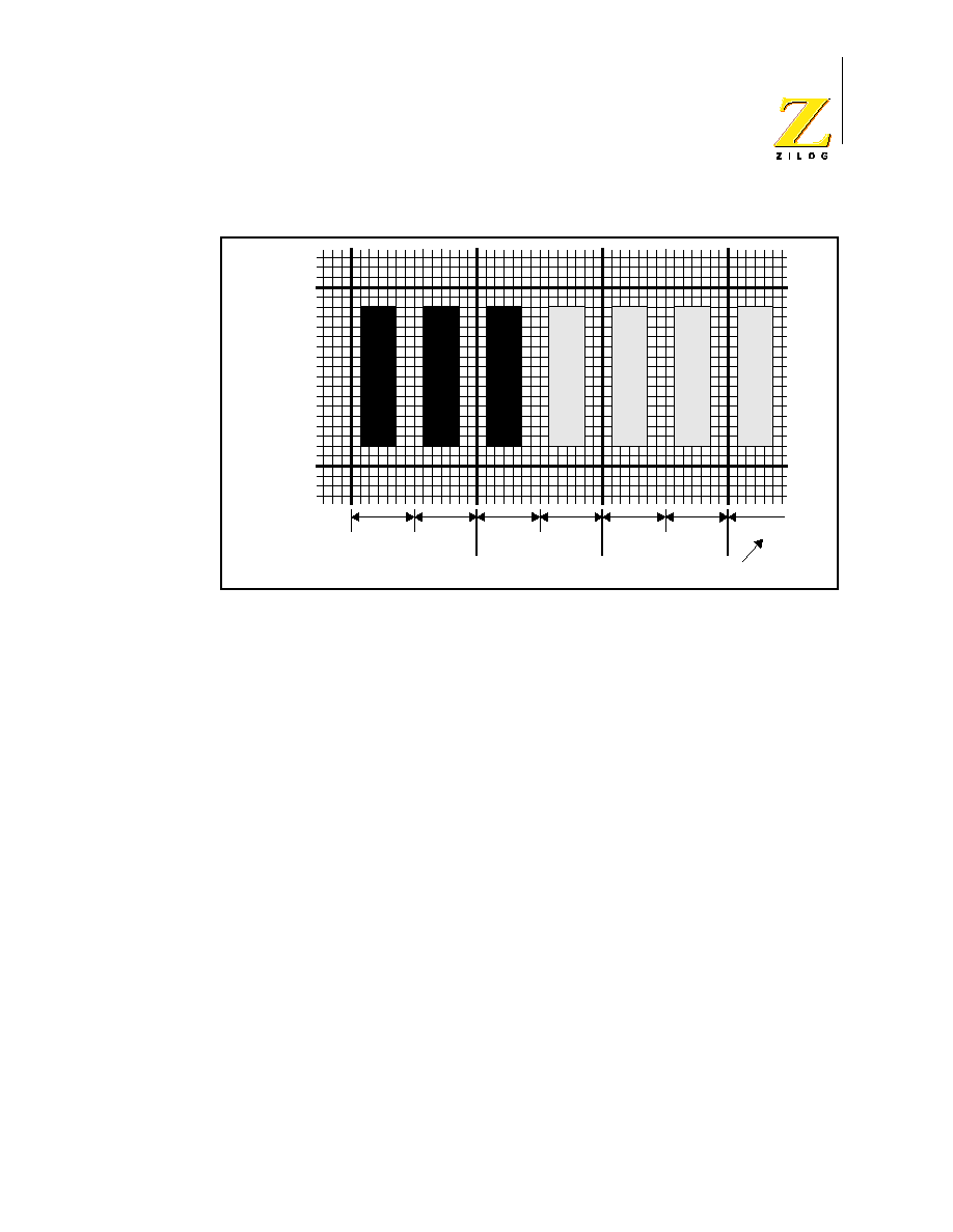
Second Color Display
5.3
Mesh and Halftone Effect
Mesh is a grid-like area that contains an alternating pixel display of OSD and
transparent zones. See Figure 10. The transparent zones allow the TV signal
display to appear in part while the mesh display is active.
Halftone effect is a transparent area that appears slightly darker than the regular
picture carried by the TV signal.
Mesh and halftone effects both serve as backgrounds for menus, action bars, and
other On-Screen Displays. The mesh feature is only for interlaced-mode video
systems.
Mesh can be controlled in two ways: through hardware or through software for
alternating pixel display in different fields.
7th Row
8 th Row
9th Row
1st Column
2nd Column
3rd Column
(3)
(4 )
(5)
(6)
(7)
(8)
(9)
Bar Column Position
Z90255 ROM and Z90251 OTP
32 KB Television Controller with OSD
PS001301-0800
29
Figure 10 Mesh On
General descriptions of the registers used to control the mesh are contained in
Tables 13 through 16.
Table 13 Mesh Column Start Register 04h: Bank F (MC_St)
Bit
7
6
5
4
3
2
1
0
R/W
R/W
R/W
R/W
R/W
R/W
R/W
R/W
R/W
Reset
x
x
x
0
0
0
0
0
Note: R = Read W = Write X = Indeterminate
Picture Screen
Field 1
Field 2
Mesh On (Mesh Color)
OSD
Fringing
Mesh

Z90255 ROM and Z90251 OTP
32 KB Television Controller with OSD
PS001301-0800
30
MC_St
and
MC_End
define the width and horizontal position of the mesh window.
Bit/
Field
Bit
Position
R/W
Value
Description
Reserved
7, 6, 5
R
W
Return
1
No effect
Mesh Window Start
4, 3, 2, 1, 0
R/W
Defines the start character
number in the mesh window.
Table 14 Mesh Column End Register 05h: Bank F (MC_End)
Bit
7
6
5
4
3
2
1
0
R/W
R/W
R/W
R/W
R/W
R/W
R/W
R/W
R/W
Reset
x
x
x
0
0
0
0
0
Note: R = Read W = Write X = Indeterminate
Bit/
Field
Bit
Position
R/W
Value
Description
Reserved
7, 6, 5
R
W
Return
1
No effect
Mesh Window End
4, 3, 2, 1, 0 R/W
Defines the character number after
the mesh window display.
Table 15 Mesh Row Enable Register 06h: Bank F (MR_En)
Bit
7
6
5
4
3
2
1
0
R/W
R/W
R/W
R/W
R/W
R/W
R/W
R/W
R/W
Reset
0
0
0
0
0
0
0
0
Note: R = Read W = Write X = Indeterminate

Z90255 ROM and Z90251 OTP
32 KB Television Controller with OSD
PS001301-0800
31
Bits
7
,
6
,
5
, and
4
,
VBLANK
Delay, set the amount of time that the
VBLANK
signal
is properly aligned with the
OSD
RGB output with delay from external circuitries.
Bit
3
, Character Foreground for Halftone Effect, defines whether displaying a
foreground color for character display is included. If bit
3
is set to
0
, halftone is
disabled for pixels with foreground color. If bit
3
is set to
1
, halftone is active for
pixels with both foreground and background colors.
Bit
0
, Mesh Window Row, sets the mesh effect to
On
or
Off
for the next row of the
OSD
.
Bit/
Field
Bit
Position R/W
Value
Description
V
BLANK
Delay
7, 6, 5, 4
R/W
0000
0001
0010
0011
0100
0101
0110
0111
1000
1001
1010
1011
1100
1101
1110
1111
No Delay
Delay by 0.5 Dot-Clock Period
Delay by 1.0 Dot-Clock Period
Delay by 1.5 Dot-Clock Period
Delay by 2.0 Dot-Clock Period
Delay by 2.5 Dot-Clock Period
Delay by 3.0 Dot-Clock Period
Delay by 3.5 Dot-Clock Period
Delay by 4.0 Dot-Clock Period
Delay by 4.5 Dot-Clock Period
Delay by 5.0 Dot-Clock Period
Delay by 5.5 Dot-Clock Period
Delay by 6.0 Dot-Clock Period
Delay by 6.5 Dot-Clock Period
Delay by 7.0 Dot-Clock Period
Delay by 7.5 Dot-Clock Period
Foreground Character for
Halftone Effect
3
R/W
0
1
Not included
Included
Reserved
2, 1
R/W
Must be 0
Mesh Window Row
0
R/W
0
1
No mesh OSD for Next Row
Mesh OSD for Next Row
Table 16 Mesh Control Register 07h: Bank F (MC_Reg)
Bit
7
6
5
4
3
2
1
0
R/W
R/W
R/W
R/W
R/W
R/W
R/W
R/W
R/W
Reset
0
0
0
0
0
0
0
0
Note: R = Read W = Write X = Indeterminate

Z90255 ROM and Z90251 OTP
32 KB Television Controller with OSD
PS001301-0800
32
When working with Progressive mode, mesh does not work the
same way as in Interlace mode.
Bit
7
, Halftone Output Delay on
P20
, is the amount of time that output of the
halftone signal is delayed to compensate for the amount of delay of
OSD
RGB
from external circuitries.
Bits
6
,
5
, and
4
, Mesh Color, define the color of the mesh window. The colors are
specified in Blue, Green, Red order, as shown in Table 17.
Bit/
Field
Bit
Position R/W
Value
Description
Halftone Effect Output
Delay on P20
7
R/W
xx/x
00/0
00/1
01/0
01/1
10/0
10/1
11/0
11/1
Bits 5, 4 in ROW_SPACE/ bit 7
No Delay
Delay by 0.5 Dot-Clock Period
Delay by 1.0 Dot-Clock Period
Delay by 1.5 Dot-Clock Period
Delay by 2.0 Dot-Clock Period
Delay by 2.5 Dot-Clock Period
Delay by 3.0 Dot-Clock Period
Delay by 3.5 Dot-Clock Period
Mesh Color
6, 5, 4
R/W
Defines the mesh color.
B,G,R respectively.
P20 for
Halftoning
3
R/W
0
1
Normal Mesh effect
Use P20 Output for Halftoning
Software Field Number/
Polarity of Halftone
Effect Output
2
R/W
0
1
Even Field/Positive Halftone Effect
Output
Odd Field/Negative Halftone Effect
Output
Software Mesh
1
R/W
0
1
Hardware Defines Field Number
Software Defined Field Number
Mesh Enable
0
R/W
0
1
Mesh is Disabled
Mesh is Enabled

Z90255 ROM and Z90251 OTP
32 KB Television Controller with OSD
PS001301-0800
33
Bit
3
,
P20
for Halftone, selects mesh or halftone effect. If bit
3
is set to
1, P20
outputs halftone. If reset to
0,P20
is a normal I/O pin.
Bit
2
, Software Field Number/Polarity of Halftone Output, has several possible
values. The value of this bit remains the same for the entire mesh window; it does
not change from row to row.
If bit
3
is set to
1
(halftone), bit
2
defines the polarity of halftone output. If bit
3
is
reset to
0
and bit
1
is set to
1
, then bit
2
defines the field number (even or odd).
Bit
1
, Software Mesh, defines whether hardware or software sets the current field
number. When the value equals
0
, hardware defines field number. When the
value equals
1
, software defines the field number.
Bit
0
, Mesh Enable, disables or enables using mesh. This field is used in
conjunction with
MR_EN (0)
. The value of Mesh Enable is changed only when
Mesh Window Row equals
0
(the current
OSD
row is not part of a mesh window). If
the value is changed when the current row is part of the mesh window, partial or
missing characters are likely to be displayed.
5.4
OSD Fade
Fading is the gradual disappearance of the
OSD
. Fading occurs vertically, up or
down. Figure 11 shows the fade-down effect.
Fade control registers can only be updated during
V
SYNC
, not during row interrupt.
Otherwise, unexpected results can occur.
Table 17 BGR Mesh Colors
B
G
R
Color
0
0
0
Black
0
0
1
Red
0
1
0
Green
0
1
1
Yellow
1
0
0
Blue
1
0
1
Magenta
1
1
0
Cyan
1
1
1
White
Z90255 ROM and Z90251 OTP
32 KB Television Controller with OSD
PS001301-0800
34
Figure 11
Video Fade (Example)
This feature is controlled through the
FADE_POS1
(Table 18),
FADE_POS2
(Table
19), and
ROW_SPACE
registers (Table 20).
Z90255 ROM and Z90251 OTP
32 KB Television Controller with OSD
PS001301-0800
35
Bits
3, 2, 1,
and
0
define the boundary row for the fade area. The portion of
the
OSD
above or below the row number fades up or down, as set in Fade
Direction,
ROW_SPACE(6)
.
The fade starts at the scan line set in
FADE_POS2 (4,3,2,1,0
) within the row
number set in
FADE_POS1 (3,2,1,0).
Table 18 Fade Position Register 1 05h: Bank A (FADE_POS1)
Bit
7
6
5
4
3
2
1
0
R/W
R/W
R/W
R/W
R/W
R/W
R/W
R/W
R/W
Reset
1
1
1
1
0
0
0
0
Note: R = Read W = Write X = Indeterminate
Bit/
Field
Bit
Position
R/W
Value Description
Reserved
7, 6, 5, 4
R
W
Return
1
No effect
Row Number of the Screen
3, 2, 1, 0
R/W
OSD Row number for fading
Table 19 Fade Position Register 2 06h: Bank A (FADE_POS2)
Bit
7
6
5
4
3
2
1
0
R/W
R/W
R/W
R/W
R/W
R/W
R/W
R/W
R/W
Reset
1
1
1
0
0
0
0
0
Note: R = Read W = Write X = Indeterminate
Bit/
Field
Bit
Position
R/W
Value
Description
Reserved
7, 6, 5
R
W
Return
1
No effect
Scan Line Number
4, 3, 2, 1, 0
R/W
Scan Line Number of a row

Z90255 ROM and Z90251 OTP
32 KB Television Controller with OSD
PS001301-0800
36
5.5
Inter-Row Spacing
Inter-Row Spacing can be from
0
to
15
horizontal scan line (HL). A setting of
0
HL
is called Continuous Row Display. A horizontal interrupt is generated at the
start of each row. Software must program the spacing between the current row
and the next row during the current horizontal interrrupt.
The time required to process a row must not exceed the display time of the row.
Refer to Table 20.
Bit
7
, Fade ON/OFF, disables or enables the fade effect.
Bit
6
, Fade Direction, controls the direction of the fade effect. When Fade
Direction is set to
0
, the bottom of the TV screen is faded out. Fading occurs
beginning with the row number set in
FADE_POS1 (3,2,1,0)
and the scan line
number set in
FADE_POS2 (4,3,2,1,0)
. When the Fade Direction is set to
1
,
the top of the screen is faded out.
Bits
5
and
4
, Halftone Effect Delay on
P20
, work with
MC_REG (7)
.
Bits
3,
2,
1,
and
0
, Inter-Row Space, specify the number of
HL
to add between
displayed rows.
Table 20 Row Space Register 04h: BankA (ROW_SPACE)
Bit
7
6
5
4
3
2
1
0
R/W
R/W
R/W
R/W
R/W
R/W
R/W
R/W
R/W
Reset
0
0
0
0
0
0
0
0
Note: R = Read W = Write X = Indeterminate
Bit/
Field
Bit
Position R/W
Value
Description
Fade On/Off
7
R/W
0
1
Fade feature disabled
Fade feature enabled
Fade Direction
6
R/W
0
1
Fade area below the defined fade
position
Fade area above the defined
fade position
Halftone Effect Output
Delay On P20
5, 4
R/W
Works with bit 7 in MC_Reg
Inter-Row Space
3, 2, 1, 0
R/W
Inter row spacing
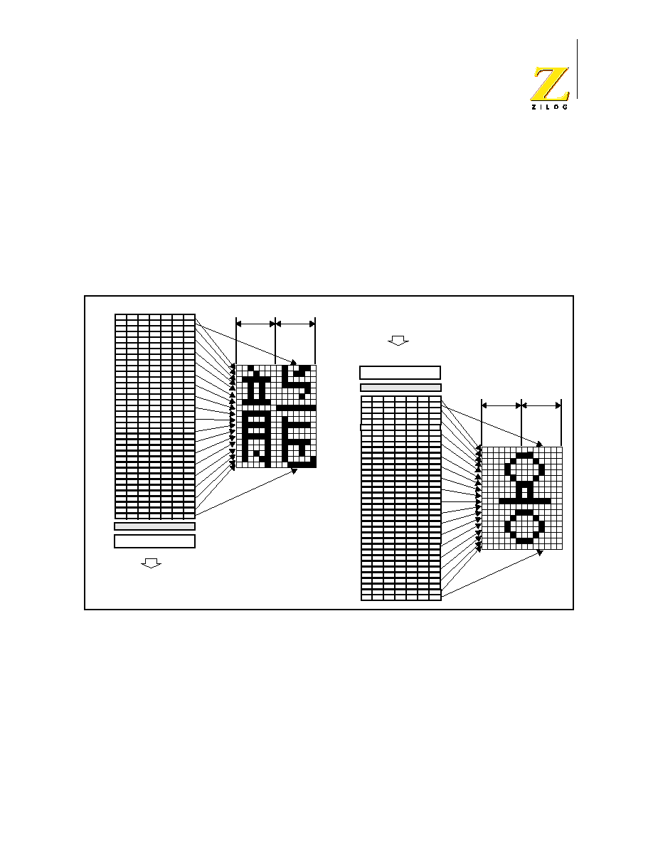
Z90255 ROM and Z90251 OTP
32 KB Television Controller with OSD
PS001301-0800
37
5.6
Character Generation
Character generation provides the content of the
OSD
. The Z90255 supports 14-
pixel (horizontal) by 18-pixel (vertical) character display with 512 character sets.
Character Cell Resolution
Characters are mapped pixel-by-pixel in Character Generation Read-Only
Memory (
CGROM
).
Figure 12 Character Pixel map in CGROM
Figure 12 is an example of a 512 character set where the character pixel map
represents the first and last characters. It is 14 pixels horizontal and 18 pixels
vertical. Each row in the map is 7 bits long, half the width of the character scan
line.
Even numbered rows in the map correspond to pixels on the left half of the
character scan line; odd rows in the map correspond to pixels on the right half of
the character scan line.
0
0
1
0
0
0
0
0
1
0
0
1
1
0
0
0
0
1
0
0
0
0
1
0
1
1
0
0
0
1
1
1
1
1
0
0
1
0
0
0
0
0
0
0
1
0
1
0
0
0
1
1
1
1
1
0
0
0
1
0
1
0
0
0
0
0
0
0
1
0
0
0
1
0
1
0
0
0
0
0
0
1
0
0
0
1
1
1
1
1
0
0
0
0
0
0
0
0
0
0
0
0
0
0
0
1
1
1
1
1
1
1
0
1
1
1
1
1
0
0
0
0
0
0
0
0
0
1
0
0
0
1
0
0
1
0
0
0
0
0
0
1
1
1
1
1
0
0
1
1
1
1
1
0
0
1
0
0
0
1
0
0
1
0
0
0
0
0
0
1
1
1
1
1
0
0
1
0
0
0
0
0
0
1
0
0
0
1
0
0
1
1
1
1
1
0
0
1
0
0
0
1
0
0
1
0
0
1
0
0
0
1
0
1
0
1
0
0
1
0
0
1
0
0
0
1
0
0
1
1
0
0
1
0
0
0
0
1
0
0
0
0
0
1
0
0
0
1
1
1
1
1
0000
0001
0002
0003
0004
0005
0006
0007
0008
0009
000a
000b
000c
000d
000e
000f
0010
0011
0012
0013
0014
0015
0016
0017
0018
0019
001a
001b
001c
001d
001e
001f
0020
0021
0022
0023
0040
0063
Hex Add
Left Half
Right Half
0024
0039
0
0
0
0
0
0
0
0
0
0
0
0
0
0
0
0
0
0
0
0
1
1
1
0
0
0
0
0
0
0
0
0
0
1
0
0
0
1
0
0
0
0
0
0
0
0
1
0
0
0
0
0
1
0
0
0
0
0
0
0
1
0
0
0
0
0
1
0
0
0
0
0
0
0
0
1
0
0
0
1
0
0
0
0
0
0
0
0
0
0
1
1
1
0
0
0
0
0
0
0
0
0
0
0
1
0
1
0
0
0
0
0
0
0
0
0
0
0
1
0
1
0
0
0
0
0
0
0
0
1
1
1
1
1
1
1
1
1
0
0
0
0
0
0
0
0
0
0
0
0
0
0
0
0
0
0
0
0
0
0
1
1
1
0
0
0
0
0
0
0
0
0
0
1
0
0
0
1
0
0
0
0
0
0
0
0
1
0
0
0
0
0
1
0
0
0
0
0
0
0
1
0
0
0
0
0
1
0
0
0
0
0
0
0
0
1
0
0
0
1
0
0
0
0
0
0
0
0
0
0
1
1
1
0
0
0
0
0
0
0
0
0
0
0
0
0
0
0
0
0
0
0
7fc0
7fc1
7fc2
7fc3
7fc4
7fc5
7fc6
7fc7
7fc8
7fc9
7fca
7fcb
7fcc
7fcd
7fce
7fcf
7fd0
7fd1
7fd2
7fd3
7fd4
7fd5
7fd6
7fd7
7fd8
7fd9
7fda
7fdb
7fdc
7fdd
7fde
7fdf
7fe0
7fe1
7fe2
7fe3
Left Half
Right Half
7fc0
7fa4
7fbf
7fa3
address GAP
address GAP
Character Pattern
Character Pattern
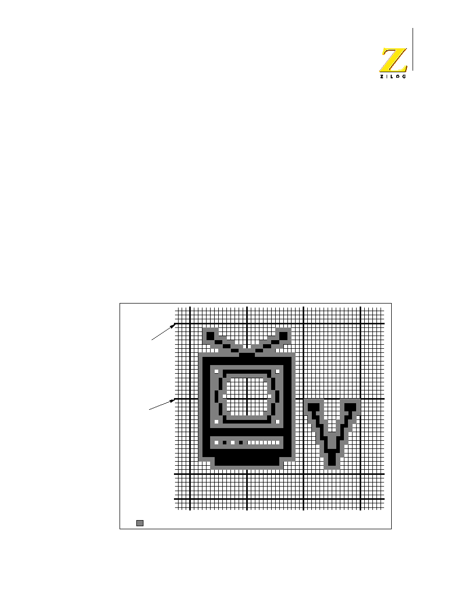
Z90255 ROM and Z90251 OTP
32 KB Television Controller with OSD
PS001301-0800
38
The Hex Add column is a hexadecimal number that serves as an address for the
group of pixels from the starting point of the scan line. Addressing begins at
0000h
and ends at
0023h
for the first character. There is an address gap
between characters. The starting address for the second character is
0040h
.
Each bit in the map sets the foreground/background designation of the
corresponding pixel:
0
background pixel
1
foreground pixel
The patterns formed by the bits comprise the characters that are displayed when
the scan line is output to the screen.
Each of these character pixel maps is one character; 512 characters can be
mapped.
Several characters can be combined to form a large icon. Figures 13 is an
example of a large icon. Each block marked by the darker grid lines is 14 x 18
pixels, one character.
Figure 13 Example of a Multiple Character Icon
Row 5
Row 6
6HL
Spacing
Row 7
Fringing Effect
No Spacing
No spacing
Row 4
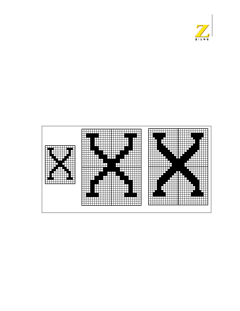
Z90255 ROM and Z90251 OTP
32 KB Television Controller with OSD
PS001301-0800
39
5.7
Character Size and Smoothing Effect
The Z90255 supports four character sizes: 1X, 2X, double width, and double
height. The 2X size duplicates each pixel horizontally and vertically to reach
double size. Figure 14 shows a character at 1X, 2X without smoothing, and 2X
with smoothing.
Smoothing means enhancing a character to improve its appearance. This effect
can be applied to 2X and double width characters, and is enabled and disabled in
DISP_ATTR: 03h: Bank A (4).
Check the effect of smoothing on 2X and double width characters before finalizing
OSD
programming.
Figure 14 Smoothing Effect on 2X Character Size
2X
After Smoothing
1X

Z90255 ROM and Z90251 OTP
32 KB Television Controller with OSD
PS001301-0800
40
5.8
Fringing Effect
Fringing means surrounding a character with a different color than the foreground
and background colors. Refer back to Figure 8. Fringing adds visual appeal to the
character presentation.
The fringing effect is enabled or disabled in
DISP_ATTR: 03h: Bank A (5)
.
The fringing color is set in
INT_ST: 07h: Bank C (7)
to either
0
, the
character background color, or to
1
, a RGB color specified in
INT_ST: 07h:
Bank C (6,5,4).
The eight RGB colors available for fringing and background
are defined in Table 21.
The fringing feature is NOT available in Progressive Mode.
5.9
Display Attribute Control
Display Attribute Control determines screen display characteristics for the entire
screen, not just the
OSD
area. The background that covers the entire screen is
called the Master Background. Its color setting can be used to generate a blue
screen when the TV signal is not present. Table 22 shows the Display Attribute
Register.
Table 21 RGB Colors
R
G
B
Color
0
0
0
Black
0
0
1
Blue
0
1
0
Green
0
1
1
Cyan
1
0
0
Red
1
0
1
Magenta
1
1
0
Yellow
1
1
1
White

Z90255 ROM and Z90251 OTP
32 KB Television Controller with OSD
PS001301-0800
41
Bit
7
, Display Enable, disables or enables using foreground and background
color, and therefore character display. When this bit is set to
0
, effective space
characters are sourced from the video RAM. Background On/Off and row
background color are programmed independently. When bit
7
is set to
1
, the
actual video RAM characters are displayed.
Bit
6
, Master Background Enable, disables or enables using a background color
for the entire screen instead of the broadcast signal. If this bit is set to
1
, the
incoming video signal blanks and the screen background displays color according
to the background color bits. The color is specified in bits
2,
1,
0
. If bit
6
is set to
0
, the incoming video signal is displayed.
Table 22 Display Attribute Register 03h: Bank A (DISP_ATTR)
Bit
7
6
5
4
3
2
1
0
R/W
R/W
R/W
R/W
R/W
R/W
R/W
R/W
R/W
Reset
0
0
0
0
0
0
0
0
Note: R = Read W = Write X = Indeterminate
Bit/
Field
Bit
Position R/W
Value
Description
Character Display
7
R/W
0
1
Disable Character Display
Enable Character Display
Master
Background Enable
6
R/W
0
1
No Master Background
Incoming video is swapped with
the background color
Fringe Effect Enable
5
R/W
0
1
Fringe Effect is Disabled
Fringe Effect is Enabled
Smoothing Effect
Enable
4
R/W
0
1
Smoothing enabled
Smoothing disabled
RGB Polarity
3
R/W
0
1
Positive
Negative
Red Master
Background
2
R/W
See Table 21
Green Master
Background
1
R/W
See Table 21
Blue Master
Background
0
R/W
See Table 21
Z90255 ROM and Z90251 OTP
32 KB Television Controller with OSD
PS001301-0800
42
Bit 5, Fringe Enable, sets the fringe effect ON or OFF.
Bit 4, Smoothing Effect Enable, sets smoothing ON or OFF, and is available for
2X and double width characters.
Bit
3
, RGB Polarity, sets color polarity of
OSD
color output signals to positive or
negative.
Bits
2,
1,
and
0
form the color for the master background. The eight possible
colors are the same ones listed in Table 21.
Video Refresh RAM Access
The Z90255 supports 12-bit character data. Nine bits,
P8
and
P7
through
P0
,
contain character code. Three additional bits,
C2
through
C0
, contain color palette
information. See Figures 15.
Color Palette Selection bits serve as a 3-bit Color Index to the color palette look-
up table. When software writes Character Byte data (
7-0
) into VRAM, it also
takes the data in the color index register and writes the corresponding Color
Palette Selection Bits (
10-8
) and the most significant bit of character data (
P8
).
When updating 3-bit color index data, the most significant bit of the character data
must also be updated. Table 20 contains VRAM structure and memory mapping.
Figure 15 VRAM Data Path for 512 Character Set
D0
D1
D2
D3
D4
D5
D6
D7
Color Index Register
Character Information
512 Character
Set
VRAM D[11:0]
(4+8=12-bit word)
10
9
8
7
6
5
4
3
2
1
0
11
C2 C1
C0
P8
P7
P6
P5
P4 P3
P2 P1
P0
CLR_IDX: 09h Bank C
P[8:0] = character code
C[2:0] = character color
Character
color
Character code

Z90255 ROM and Z90251 OTP
32 KB Television Controller with OSD
PS001301-0800
43
Table 23 VRAM Structure and Memory Map
Character Code Data Bit[11] ,
Character Color C[2:0]
Character Code Data Bit[7:0]
Row 0 Attribute(ROW0_ATTR)
FC00h
Row0/Column 0 D[11:8]
FE01h
Row 0/Column 0 D[7:0]
FC01h
Row0/Column 1 through 22 D[11:8]
FE02h
Row 0/Column 1 through 22 D[7:0]
FC02h
FE17h
FC17h
Row 0/Column 23 D[11:8]
FE18h
Row 0/Column 23 D[7:0]
FC18h
Row 1 Attribute(ROW1_ATTR)
FC20h
Row1/Column 0 D[11:8]
FE21h
Row 1/Column 0 D[7:0]
FC21h
Row1/Column 1 through 22 D[11:8]
FE22h
Row 1/Column 1 through 22 D[7:0]
FC22h
FE37h
FC37h
Row 1/Column 23 D[11:8]
FE38h
Row 1/Column 23 D[7:0]
FC38h
Row 2 Video RAM buffer
FC40h
Row 2 D[11:8]
FE41h
FC41h
FE58h
FC58h
Row 3 Video RAM buffer
FC60h
Row 3 D[11:8]
FE61h
FC61h
FE78h
FC78h
Row 4 Video RAM buffer
FC80h
Row 4 D[11:8]
FE81h
FC81h
FE98h
FC98h
Row 5 Video RAM buffer
FCA0h
Row 5 D[11:8]
FEA1h
FCA1h
FEB8h
FCB8h

Z90255 ROM and Z90251 OTP
32 KB Television Controller with OSD
PS001301-0800
44
Hardware processes the entire 12 bits of data at the same time it processes the
OSD.
The Color Palette Selection Bits (
10-8
) are decoded as described in Table 24.
Row 6 Video RAM buffer
FCC0h
Row 6 D[11:8]
FEC1h
FCC1h
FED8h
FCD8h
Row 7 Video RAM buffer
FCE0h
Row 7 D[11:8]
FEE1h
FCE1h
FEF8h
FCF8h
Row 8 Video RAM buffer
FD00h
Row 8 D[11:8]
FF01h
FD01h
FF18h
FD18h
Row 9 Video RAM buffer
FD20h
Row 9 D[11:8]
FF21h
FD21h
FF38h
FD38h
Table 23 VRAM Structure and Memory Map (Continued)
Character Code Data Bit[11] ,
Character Color C[2:0]
Character Code Data Bit[7:0]

Z90255 ROM and Z90251 OTP
32 KB Television Controller with OSD
PS001301-0800
45
There are eight different foreground/background palettes, including the
000h
case
that reads the color(s) from the
ROW_ATTR
register mapped into video RAM.
Color Table and Color Index Register
Table 25 lists the bits in the Color Index Register.
When the Color Index has a value other than
000h
, the value indicates the
number of the color palette that contains the RGB foreground and background
colors to be displayed. In the Color Palette register descriptions below, the
following notation is used:
Table 24 Color Palette Selection Bits
Color Index, Bit [10:8]
Function
000
Selects background/foreground color in row attribute
001
Selects color palette 0 in the color look-up table
010
Selects color palette 1 in the color look-up table
011
Selects color palette 2 in the color look-up table
100
Selects color palette 3 in the color look-up table
101
Selects color palette 4 in the color look-up table
110
Selects color palette 5 in the color look-up table
111
Selects color palette 6 in the color look-up table
Table 25 Color Index Register 09h: Bank C (CLR_IDX)
Bit
7
6
5
4
3
2
1
0
R/W
R/W
R/W
R/W
R/W
R/W
R/W
R/W
R/W
Reset
1
1
1
1
0
0
0
0
Note: R = Read W = Write X = Indeterminate
Bit/
Field
Bit
Position R/W
Value Description
Reserved
7, 6, 5, 4
R
W
Return 1
No Effect
Color Index
Data
3, 2, 1, 0
R/W
Bit 3 defines MSb of the character pointer data bit
and bit [2:0] for character color data bits

Z90255 ROM and Z90251 OTP
32 KB Television Controller with OSD
PS001301-0800
46
The registers for color palettes 0 through 6 are listed in Table 26 through Table 32.
R
nf
R - Red,
n - Palette Number,
f - Foreground
R
nb
R - Red,
n - Palette Number,
b - Background
G
nf
G - Green,
n - Palette Number,
f - Foreground
G
nb
G - Green,
n - Palette Number,
b - Background
B
nf
B - Blue,
n - Palette Number,
f - Foreground
B
nb
B - Blue,
n - Palette Number,
b - Background
Table 26 Color Palette 0 Register 09h: Bank A (CLR_P0)
Bit
7
6
5
4
3
2
1
0
R/W
R/W
R/W
R/W
R/W
R/W
R/W
R/W
R/W
Reset
1
1
0
0
0
0
0
0
Note: R = Read W = Write X = Indeterminate
Bit/
Field
Bit
Position
R/W
Value Description
Reserved
7, 6
R
W
Return 1
No Effect
Color Palette 0
5,4,3,2,1,0 R/W
Programming R
0f
, G
0f
, B
0f
, R
0b
, G
0b
, B
0b
Table 27 Color Palette 1 Register 0Ah: Bank A (CLR_P1)
Bit
7
6
5
4
3
2
1
0
R/W
R/W
R/W
R/W
R/W
R/W
R/W
R/W
R/W
Reset
1
1
0
0
0
0
0
0
Note: R = Read W = Write X = Indeterminate
Bit/
Field
Bit
Position
R/W
Value Description
Reserved
7, 6
R
W
Return 1
No Effect
Color Palette 1
5,4,3,2,1,0
R/W
Programming R
1f
, G
1f
, B
1f
, R
1b
, G
1b
, B
1b

Z90255 ROM and Z90251 OTP
32 KB Television Controller with OSD
PS001301-0800
47
Table 28 Color Palette 2 Register 0Bh: Bank A (CLR_P2)
Bit
7
6
5
4
3
2
1
0
R/W
R/W
R/W
R/W
R/W
R/W
R/W
R/W
R/W
Reset
1
1
0
0
0
0
0
0
Note: R = Read W = Write X = Indeterminate
Bit/
Field
Bit
Position
R/W
Value Description
Reserved
7, 6
R
W
Return 1
No Effect
Color Palette 2
5,4,3,2,1,0
R/W
Programming R
2f
, G
2f
, B
2f
, R
2b
, G
2b
, B
2b
Table 29 Color Palette 3 Register 0Ch: Bank A (CLR_P3)
Bit
7
6
5
4
3
2
1
0
R/W
R/W
R/W
R/W
R/W
R/W
R/W
R/W
R/W
Reset
1
1
0
0
0
0
0
0
Note: R = Read W = Write X = Indeterminate
Bit/
Field
Bit
Position
R/W
Value Description
Reserved
7, 6
R
W
Return 1
No Effect
Color Palette 3
5,4,3,2,1,0
R/W
Programming R
3f
, G
3f
, B
3f
, R
3b
, G
3b
, B
3b
Table 30 Color Palette 4 Register 0Dh: Bank A (CLR_P4)
Bit
7
6
5
4
3
2
1
0
R/W
R/W
R/W
R/W
R/W
R/W
R/W
R/W
R/W
Reset
1
1
0
0
0
0
0
0
Note: R = Read W = Write X = Indeterminate

Z90255 ROM and Z90251 OTP
32 KB Television Controller with OSD
PS001301-0800
48
Bit/
Field
Bit
Position
R/W
Value Description
Reserved
7, 6
R
W
Return 1
No Effect
Color Palette 4
5,4,3,2,1,0
R/W
Programming R
4f
, G
4f
, B
4f
, R
4b
, G
4b
, B
4b
Table 31 Color Palette 5 Register 0Eh: Bank A (CLR_P5)
Bit
7
6
5
4
3
2
1
0
R/W
R/W
R/W
R/W
R/W
R/W
R/W
R/W
R/W
Reset
1
1
0
0
0
0
0
0
Note: R = Read W = Write X = Indeterminate
Bit/
Field
Bit
Position
R/W Value Description
Reserved
7, 6
R
W
Return 1
No Effect
Color Palette 5 5,4,3,2,1,0
R/W
Programming R
5f
, G
5f
, B
5f
, R
5b
, G
5b
, B
5b
Table 32 Color Palette 6 Register 0Fh: Bank A (CLR_P6)
Bit
7
6
5
4
3
2
1
0
R/W
R/W
R/W
R/W
R/W
R/W
R/W
R/W
R/W
Reset
1
1
0
0
0
0
0
0
Note: R = Read W = Write X = Indeterminate
Bit/
Field
Bit
Position
R/W
Value Description
Reserved
7, 6
R
W
Return 1
No Effect
Color Palette 6 5,4,3,2,1,0
R/W
Programming R
6f
, G
6f
, B
6f
, R
6b
, G
6b
, B
6b

Z90255 ROM and Z90251 OTP
32 KB Television Controller with OSD
PS001301-0800
49
Row Attribute Register
The Row Attribute Register (Table 33) is mapped to
VRAM
, as shown in Table 20.
This register controls row background and foreground display. If the Color Index is
set to
000h
, the display color is read from the Row Attribute Register.
5.10 HV Interrupt Processing
An interrupt is issued at the beginning of a row and at the leading edge of the
V
SYNC
signal. The leading edge of the first
H
SYNC
of a row constitutes the
beginning of a row. The Z90255 software tracks this cycle as two recurring events,
the Horizontal (
H
SYNC
) Interrupt and the Vertical (
V
SYNC
) Interrupt.
A
V
SYNC
interrupt marks the time for displaying a new field of a TV frame.
Displaying subsequent rows coincides with the issuance of the
H
SYNC
interrupt.
The interrupts mark the time when displaying a row or start of a field is to occur.
Each text row is comprised of 18 scan lines. Each scan line takes 63.5 µs to be
displayed. So, 1143 µs is the amount of time available to change programming for
the next row. Double-size and double-height characters span 36 scan lines,
Table 33 Row Attribute Register (ROW_ATTR)
Bit
7
6
5
4
3
2
1
0
R/W
R/W
R/W
R/W
R/W
R/W
R/W
R/W
R/W
Reset
x
x
x
x
x
x
x
x
Note: R = Read W = Write X = Indeterminate
Bit/
Field
Bit
Position R/W
Value Description
Row Foreground
Enable
7
R/W
0
1
Row Foreground Color displayed
Row Foreground color disabled
Row Foreground
Color
6, 5, 4
R/W
Defines the Character Color R, G, B,
respectively
Row Background
Enable
3
R/W
0
1
Row Background Color disabled
Row Background color displayed
Row Background
Color
2, 1, 0
R/W
Defines the Row Background Color R,
G, B, respectively

Z90255 ROM and Z90251 OTP
32 KB Television Controller with OSD
PS001301-0800
50
allowing 2286 µs to program the next row. Additional programming time is
available with inter-row spacing.
VRAM
is updated during that time.
If the program has too much to display, black lines appear at the top of the screen.
The HV Interrupt Status Register (Table 34) keeps track of the type of interrupt
issued, horizontal or vertical.
Bit
7
, Fringe Color Selection, sets the fringe color to the background color or to a
Red, Green, and Blue color specified in bits
6,5,4.
Bit
3
, Palette Mode, sets color to Normal or VRAM Mode. When the value is
0
(Normal Mode), the color attribute of a row is controlled by values in the
ROW_ATTR
register which is mapped in
VRAM
, but the Color Palette Selection Bits
Table 34 HV Interrupt Status Register 07h: Bank C (INT_ST)
Bit
7
6
5
4
3
2
1
0
R/W
R/W
R/W
R/W
R/W
R/W
R/W
R/W
R/W
Reset
0
0
0
0
0
0
0
0
Note: R = Read W = Write X = Indeterminate
Bit/
Field
Bit
Position R/W Value Description
Fringe Color Selection
7
R/W
0
1
Select Character Background Color
Select Fringe Color RGB*
Fringe Color
6, 5, 4
R/W
Defines Fringe Color RGB
Palette Mode
3
R/W
0
1
Normal Mode
Color Palette Mode
Horizontal Interrupt
Enable
2
R/W
0
1
No Horizontal Interrupt
Enable Horizontal Interrupt
Vertical Interrupt
1
R
W
0
1
0
1
No Vertical Interrupt
Vertical Interrupt
No Effect
Reset Vertical Interrupt Flag
Horizontal Interrupt
0
R
W
0
1
0
1
No Horizontal Interrupt
Horizontal Interrupt
No Effect
Reset Horizontal Interrupt Flag
Note: The fringing feature is not available in Progressive Mode.

Z90255 ROM and Z90251 OTP
32 KB Television Controller with OSD
PS001301-0800
51
are ignored. When the Palette Mode value is
1
, the Color Palette Selection Bits
are used, unless they are set to
0
s. In that case, the values in the
ROW_ATTR
register are used.
Bit
2
, Horizontal Interrupt Enable, disables or enables the horizontal (
H
SYNC
)
interrupt.
Bit
1
, Vertical Interrupt, has different meanings depending on its Read and Write
status. In Read State, a value of
0
indicates that a vertical interrupt was not
issued; a value of
1
indicates that a vertical interrupt was issued. In Write State, a
value of
0
has no effect; a value of
1
resets the vertical interrupt flag.
Bit
0
, Horizontal Interrupt, has different meanings depending on its status. In
Read State, a value of
0
indicates that a horizontal interrupt was not issued; a
value of
1
indicates that a horizontal interrupt was issued. In Write State, a value
of
0
has no effect; a value of
1
resets the horizontal interrupt flag.
When an interrupt is issued while another interrupt is processing, the last-issued
interrupt is pended. The interrupt-flag bit which is in service (the interrupt issued
first) must be cleared or serviced before the pended interrupt can be processed
(see
SNDCLR(6)
).
Z90255 ROM and Z90251 OTP
32 KB Television Controller with OSD
PS001301-0800
52
H
SYNC
and V
SYNC
Requirements
H
SYNC
and V
SYNC
must meet all TV broadcasting specifications. The minimum
width of V
SYNC
must conform to the specification in Figure 16.
Figure 16 H
SYNC
and V
SYNC
Specification
The rising edge of V
SYNC
must not coincide with the rising edge of H
SYNC
to be
sure that the controller recognizes both rising edges.
V
T
H
CYCLE
1/2 H
CYCLE
Field 1
Field 2
V
T
must be larger than 1.5 x (H
CYCLE
+H
T
).
The same timing specification must applied in negative polarity.
H
T
Z90255 ROM and Z90251 OTP
32 KB Television Controller with OSD
PS001301-0800
53
6
Z90255 I2C Master Interface
The Z90255 has a hardware module which supports the I
2
C Master interface. Bus
arbitration and Masters’ arbitration logic is NOT implemented; in other words, the
Z90255 is designed for a Single Master application.
The I
2
C interface can be configured to run at four different transfer speeds defined
by bits (
1,0
) in the I
2
C Control Register (
I
2
C_CNTL: 0Ch, Bank:C
).
To circumvent possible problems on both DATA and SCLK lines, digital filters with
time constant equal to
3T
sclk
are implemented on all inputs of the I
2
C bus
interface. The Z90255 has two separate I
2
C busses which share the same I
2
C
state machine.
The I
2
C module is enabled by setting bit (2) in the I2C_CNTL register to 1(see
Figure 17). This bit blocks out I
2
C logic if it is set to 0. To prevent switching the I
2
C
bus during activation, bits (7,6) of the Port 2 Data Register for I
2
C selection 1 (bits
(5,4) of Port 2 Data Register for I
2
C selection 0) should be set to 1 before the I
2
C
module is enabled.
1
When the I
2
C module is enabled, pins used as I
2
C must be
configured as output in the Port
2
Mode Register (
P2M:
F6h
). If
P27/P26
or
P25/P24
are used as I
2
C pins, then
these pins are automatically set to open-drain mode.
2
Port 2 must be configured in standard drive mode (
PCON:
00h: Bank F
) when the I
2
C interface is active.
Figure 17 Bidirectional Port Pin Pad Multiplexed with I2C Port
Notes:
V
CC
PAD
P2CNTL (0)
P2M
I
2
C DATA (Output)
P2 (Output)
I
2
C Enable
P2 (Input)
I
2
C Selection
I
2
C DATA (Input)
1
0 S
1 = Input
0 = Output
For I
2
C

Z90255 ROM and Z90251 OTP
32 KB Television Controller with OSD
PS001301-0800
54
If bits
4
and
5
both equal
1
, then the I
2
C Selection
0
prevails.
Controlling the I
2
C Interface
Software controls the I
2
C module by writing appropriate commands into the I
2
C
Command Register (
I
2
C_CMD:0Bh:0Ch
). See Table 36.
Table 35 Master I
2
C Control Register 0Ch: Bank C (I
2
C_CNTL)
Bit
7
6
5
4
3
2
1
0
R/W
R/W
R/W
R/W
R/W
R/W
R/W
R/W
R/W
Reset
x
x
0
0
x
x
x
x
Note: R = Read W = Write X = Indeterminate
Bit/
Field
Bit
Position
R/W
Value Description
Clock Selection
7
R/W
0
1
1X SCLK for I
2
C and ADC
0.5X SCLK for I
2
C and ADC
Reserved
6
R
W
Return
1
No Effect
I
2
C Selection 1
5
R/W
0
1
P26 selection - POR
P27 selection - POR
SCLK1 selection on P26
SDATA1 selection on P27
I
2
C Selection 0
4
R/W
0
1
P24 selection - POR
P25 selection - POR
SCLK 0 selection on P24
SDATA0 selection on P25
Reserved
3
R/W
Must be 0
I
2
C Enable
2
R/W
0
1
Disable I
2
C Interface
Enable I
2
C Interface
I
2
C Speed (for 6-MHz XTAL) 1, 0
R/W
00
01
10
11
10 KHz
50 KHz
100 KHz
330 KHz

Z90255 ROM and Z90251 OTP
32 KB Television Controller with OSD
PS001301-0800
55
Software puts data to be transmitted into I
2
C Data Register (Table 37) and reads
received data from it. Bit
7
in this register is used as an acknowledge bit when
receiving data from a Slave. Bit
0
of
I
2
C_DATA
register contains an
acknowledgment bit generated by the Slave. Refer to Table 38.
Table 36 Master I
2
C Command Register 0Bh: Bank C (I
2
C_CMD)
Bit
7
6
5
4
3
2
1
0
R/W
R/W
R/W
R/W
R/W
R/W
R/W
R/W
R/W
Reset
x
x
x
x
x
x
x
0
Note: R = Read W = Write X = Indeterminate
Bit/
Field
Bit
Position
R/W
Value Description
Reserved
7
R
W
Return 1
No Effect
I
2
C Command
6, 5, 4
R
W
Return 1
See Table 35
Reserved
3, 2
R
W
Return 1
No Effect
Reset
1
R
W
0
1
Return 1
No Effect
Reset I
2
C interface
Busy
0
R
W
0
1
Idle
Busy
No Effect
Table 37 Master I
2
C Data Register 0Ah: Bank C (I
2
C_DATA)
Bit
7
6
5
4
3
2
1
0
R/W
R/W
R/W
R/W
R/W
R/W
R/W
R/W
R/W
Reset
0
0
0
0
0
0
0
0
Note: R = Read W = Write X = Indeterminate
Bit/
Field
Bit
Position
R/W Value
Description
Data
7,6,5,4,3,2,1,0
R
W
Received data
Data to be sent

Z90255 ROM and Z90251 OTP
32 KB Television Controller with OSD
PS001301-0800
56
Table 38 Master I
2
C Bus Interface Commands
Command
Description
000
Send a Start bit followed by the address byte specified in the I
2
C data
register, then fetch the acknowledgment bit in I
2
C_DATA (0). Used to
initialize communication. Nine SCLK cycles are generated.
001
Send the byte of data specified in the I
2
C data register, then fetch an
acknowledgment bit stored in bit 0. Used in a Write frame. Nine SCLK
cycles are generated.
010
Send bit
7
of I
2
C_DATA register as an acknowledgment bit (ACK:
(0XXXXXXX), NAK: (1XXXXXXX)), then receive a data byte. Used in a
Read frame when the next data byte is expected. Nine SCLK cycles are
generated. Received data is read in the I
2
C data register.
011
Send bit
7
of I
2
C_DATA register as an acknowledgment bit (ACK:
(0XXXXXXX), NAK: (1XXXXXXX). Used in a Read frame. One SCLK
cycle is generated.
10X
Null operation. Must be used with a Reset bit.
110
Received one data byte. Used in a Read frame to receive the first data
byte after an address byte is transmitted. Eight SCLK cycles are
generated.
111
Send Stop bit. One SCLK cycle is generated.

Z90255 ROM and Z90251 OTP
32 KB Television Controller with OSD
PS001301-0800
57
7
Input/Output Ports
There are 20 input/output (I/O) ports. In addition, seven pulse-width modulators
(
PWM
),
PWM1
through
PWM6,
and
PWM11
, can be configured as regular output
ports. The maximum number of I/O ports available is 27. Please refer to the port
bank and number carefully for exact addressing and access. See Table 39
through Table 49.
Ports
2, 4,
and
6
can be set for
Standard
or
Low EMI
. The
Low EMI
option
can also be selected for the microcontroller oscillator or
OSD
oscillator. Standard
(
1
) is the High setting. Following Power-On Reset, Bits
1, 2, 5, 6, 7
each
has a value of
1
.
Table 39 Port configuration Register 00h: Bank F (PCON)
Bit
7
6
5
4
3
2
1
0
R/W
R/W
R/W
R/W
R/W
R/W
R/W
R/W
R/W
Reset
1
1
1
1
1
1
1
0
Note: R = Read W = Write X = Indeterminate
Bit/
Field
Bit
Position
R/W
Value
Description
Low EMI Z8
Oscillator
7
R/W
0
1
Low EMI Noise
Standard-POR
Low EMI Port 6
6
R/W
0
1
Low EMI Noise
Standard-POR
Low EMI Port 2
5
R/W
0
1
Low EMI Noise
Standard-POR
Reserved
4, 3
R
W
Return 1
Write 1s
Low EMI Port 4 and
PWMs
2
R/W
0
1
Low EMI Noise
Standard-POR
Low EMI OSD
Oscillator
1
R/W
0
1
Low EMI Noise
Standard-POR
Reserved
0
R/W
Return Unknown
No Effect

Z90255 ROM and Z90251 OTP
32 KB Television Controller with OSD
PS001301-0800
58
When
P27/P26
or
P25/P24
are used as I
2
C pins, then these pins are
automatically set to open-drain mode.
Table 40 Port 2 Mode Register F6h: P2M
Bit
7
6
5
4
3
2
1
0
R/W
W
W
W
W
W
W
W
W
Reset
1
1
1
1
1
1
1
1
Note: R = Read W = Write X = Indeterminate
Bit/
Field
Bit
Position
R/W
Value Description
P27 I/O Definition
7
W
0
1
Defines P27 as Output
Defines P27 as Input
P26 I/O Definition
6
W
0
1
Defines P26 as Output
Defines P26 as Input
P25 I/O Definition
5
W
0
1
Defines P25 as Output
Defines P25 as Input
P24 I/O Definition
4
W
0
1
Defines P24 as Output
Defines P24 as Input
P23 I/O Definition
3
W
0
1
Defines P23 as Output
Defines P23 as Input
P22 I/O Definition
2
W
0
1
Defines P22 as Output
Defines P22 as Input
P21 I/O Definition
1
W
0
1
Defines P21 as Output
Defines P21 as Input
P20 I/O Definition
0
W
0
1
Defines P20 as Output
Defines P20 as Input
Table 41 Port 2 Data Register 02h: P2
Bit
7
6
5
4
3
2
1
0
R/W
R/W
R/W
R/W
R/W
R/W
R/W
R/W
R/W
Reset
x
x
x
x
x
x
x
x
Note: R = Read W = Write X = Indeterminate

Z90255 ROM and Z90251 OTP
32 KB Television Controller with OSD
PS001301-0800
59
7.1
Port 4 Pin-Out Selection Register
Bits
5,4,3
, and
2
control the configuration of multiplexed pins
20
,
19
,
18
, and
17
. If a bit is set to
0
, the pin functions as a
PWM
output port. If a bit is set to
1
, the
pin functions as a programmable regular input/output port. See Table 42. This
value is the default following a Power-On Reset.
Bit/
Field
Bit
Position
R/W
Value
Description
P27
7
R
W
Data input on P27
Data Output on P27
P26
6
R
W
Data input on P26
Data Output on P26
P25
5
R
W
Data input on P25
Data Output on P25
P24
4
R
W
Data input on P24
Data Output on P24
P23
3
R
W
Data input on P23
Data Output on P23
P22
2
R
W
Data input on P22
Data Output on P22
P21
1
R
W
Data input on P21
Data Output on P21
P20
0
R
W
Data input on P20
Data Output on P20
Table 42 Port 4 Pin-Out Selection Register 08h: Bank C (PIN_SLT)
Bit
7
6
5
4
3
2
1
0
R/W
R/W
R/W
R/W
R/W
R/W
R/W
R/W
R/W
Reset
x
x
1
1
1
1
x
x
Note: R = Read W = Write X = Indeterminate

Z90255 ROM and Z90251 OTP
32 KB Television Controller with OSD
PS001301-0800
60
Bit/
Field
Bit
Position
R/W
Value
Description
Reserved
7, 6
R
W
Return 1
No Effect
P47/PWM10
5
R/W
0
1
Selects PWM10
Selects P47 - POR
P46/PWM9
4
R/W
0
1
Selects PWM9
Selects P46 - POR
P45/PWM8
3
R/W
0
1
Selects PWM8
Selects P45 - POR
P44/PWM7
2
R/W
0
1
Selects PWM7
Selects P44 - POR
Reserved
1, 0
R
W
Return 1
No Effect
Table 43 Port 4 Data Register 05h: Bank C (PRT4_DTA)
Bit
7
6
5
4
3
2
1
0
R/W
R/W
R/W
R/W
R/W
R/W
R/W
R/W
R/W
Reset
x
x
x
x
x
x
x
x
Note: R = Read W = Write X = Indeterminate
Bit/
Field
Bit
Position
R/W
Value
Description
P47
7
R
W
Data input on P47
Data Output on P47
P46
6
R
W
Data input on P46
Data Output on P46
P45
5
R
W
Data input on P45
Data Output on P45
P44
4
R
W
Data input on P44
Data Output on P44
P43
3
R
W
Data input on P43
Data Output on P43

Z90255 ROM and Z90251 OTP
32 KB Television Controller with OSD
PS001301-0800
61
P42
2
R
W
Data input on P42
Data Output on P42
P41
1
R
W
Data input on P41
Data Output on P41
P40
0
R
W
Data input on P40
Data Output on P40
Table 44 Port 4 Direction Control Register 06h: Bank C (PRT4_DRT)
Bit
7
6
5
4
3
2
1
0
R/W
R/W
R/W
R/W
R/W
R/W
R/W
R/W
R/W
Reset
1
1
1
1
1
1
1
1
Note: R = Read W = Write X = Indeterminate
Bit/
Field
Bit
Position
R/W
Value
Description
P47 I/O Definition
7
R/W
0
1
Defines P47 as Output
Defines P47 as Input-POR
P46 I/O Definition
6
R/W
0
1
Defines P46 as Output
Defines P46 as Input-POR
P45 I/O Definition
5
R/W
0
1
Defines P45 as Output
Defines P45 as Input-POR
P44 I/O Definition
4
R/W
0
1
Defines P44 as Output
Defines P44 as Input-POR
P43 I/O Definition
3
R/W
0
1
Defines P43 as Output
Defines P43 as Input-POR
P42 I/O Definition
2
R/W
0
1
Defines P42 as Output
Defines P42 as Input-POR
P41 I/O Definition
1
R/W
0
1
Defines P41 as Output
Defines P41 as Input-POR
P40 I/O Definition
0
R/W
0
1
Defines P40 as Output
Defines P40 as Input-POR
Bit/
Field
Bit
Position
R/W
Value
Description

Z90255 ROM and Z90251 OTP
32 KB Television Controller with OSD
PS001301-0800
62
7.2
Port 5 Pin-Out Selection Register
Table 45 PWM Mode Register 0Dh: Bank B (P_MODE)
Bit
7
6
5
4
3
2
1
0
R/W
R/W
R/W
R/W
R/W
R/W
R/W
R/W
R/W
Reset
0
1
1
1
1
1
1
1
Note: R = Read W = Write X = Indeterminate
Table 46 Port 5 Data Register 0Ch: Bank B (PRT5_DTA)
Bit
7
6
5
4
3
2
1
0
R/W
R/W
R/W
R/W
R/W
R/W
R/W
R/W
R/W
Reset
x
x
x
x
x
x
x
x
Note: R = Read W = Write X = Indeterminate
Bit/
Field
Bit
Position
R/W
Value
Description
Reserved
7
R
W
Return 1
No Effect
P56
6
R
W
Data input on P56
Data Output on P56
P55
5
R
W
Data input on P55
Data Output on P55
P54
4
R
W
Data input on P54
Data Output on P54
P53
3
R
W
Data input on P53
Data Output on P53
P52
2
R
W
Data input on P52
Data Output on P52
P51
1
R
W
Data input on P51
Data Output on P51
P50
0
R
W
Data input on P50
Data Output on P50

Z90255 ROM and Z90251 OTP
32 KB Television Controller with OSD
PS001301-0800
63
7.3
Port 6 Data Register
Table 47 Port 5 Direction Control Register 0Eh: Bank B (PRT5_DRT)
Bit
7
6
5
4
3
2
1
0
R/W
R/W
R/W
R/W
R/W
R/W
R/W
R/W
R/W
Reset
x
1
1
1
1
1
1
1
Note: R = Read W = Write X = Indeterminate
Bit/
Field
Bit
Position
R/W
Value
Description
Reserved
7
R
W
Return 1
No Effect
P56 I/O Definition
6
R/W
0
1
Defines P56 as Output
Defines P56 as Input-POR
P55 I/O Definition
5
R/W
0
1
Defines P55 as Output
Defines P55 as Input-POR
P54 I/O Definition
4
R/W
0
1
Defines P54 as Output
Defines P54 as Input-POR
P53 I/O Definition
3
R/W
0
1
Defines P53 as Output
Defines P53 as Input-POR
P52 I/O Definition
2
R/W
0
1
Defines P52 as Output
Defines P52 as Input-POR
P51 I/O Definition
1
R/W
0
1
Defines P51 as Output
Defines P51 as Input-POR
P50 I/O Definition
0
R/W
0
1
Defines P50 as Output
Defines P50 as Input-POR
Table 48 Port 6 Data Register 03h: Bank F (PRT6_DTA)
Bit
7
6
5
4
3
2
1
0
R/W
R/W
R/W
R/W
R/W
R/W
R/W
R/W
R/W
Reset
1
1
1
1
1
1
1
1
Note: R = Read W = Write X = Indeterminate

Z90255 ROM and Z90251 OTP
32 KB Television Controller with OSD
PS001301-0800
64
Bit/
Field
Bit
Position
R/W
Value
Description
Reserved
7, 6, 5, 4
R
W
Return Unknown
No Effect
P63
3
R
W
Data input on P63
Data Output on P63
P62
2
R
W
Data input on P62
Data Output on P62
P61
1
R
W
Data input on P61
Data Output on P61
P60
0
R
W
Data input on P60
Data Output on P60
Table 49 Port 6 Direction Control Register 02h: Bank F (PRT6_DRT)
Bit
7
6
5
4
3
2
1
0
R/W
R/W
R/W
R/W
R/W
R/W
R/W
R/W
R/W
Reset
1
1
1
1
1
1
1
1
Note: R = Read W = Write X = Indeterminate
Bit/
Field
Bit
Position
R/W
Value Description
P63
7
R/W
0
1
Open-Drain Output
Push-Pull Output - POR
P62
6
R/W
0
1
Open-Drain Output
Push-Pull Output - POR
P61
5
R/W
0
1
Open-Drain Output
Push-Pull Output - POR
P60
4
R/W
0
1
Open-Drain Output
Push-Pull Output - POR
P63 I/O
definition
3
R/W
0
1
Data Output
Data Input - POR

Z90255 ROM and Z90251 OTP
32 KB Television Controller with OSD
PS001301-0800
65
8
Infrared Interface
The Z90255 supports the Infrared (
IR
) Remote Control interface with a minimum
of software overhead.
Two bytes of data are received through the Infrared (
IR
) Interface. The lower
byte, bits
7-0
, is stored in IR Capture Register
0
. The upper byte, bits
15-8
, is
stored in IR Capture Register
1
.
When an
IR
interrupt occurs, the
IR
capture registers contain the amount of time
passed from the previous
IR
interrupt if bit
0
in the TCR0 is set to
0
. If bit
0
is set
to
1
, the
IR
capture registers contain the amount of time passed from the last
overflow of the
IR
capture counter. The
IR
interrupt flags are reset by the
IR
interrupt service routine software. Refer to Table 50 through Table 53.
Timer Control Register 0
Rising edge (falling edge) interrupt is preserved even when a falling edge (rising
edge) interrupt occurs. But it is overridden by a second rising edge (falling edge) if
the second one occurs before the first rising edge (falling edge) is serviced.
Preservation of the interrupt means that it generates the hardware interrupt after
the first interrupt is serviced when two different (rising edge/falling edge) interrupts
are already
ON
.
P62 I/O
definition
2
R/W
0
1
Data Output
Data Input - POR
P61 I/O
definition
1
R/W
0
1
Data Output
Data Input - POR
P60 I/O
definition
0
R/W
0
1
Data Output
Data Input - POR
Table 50 Timer Control Register 0 01h: Bank C (TCR0)
Bit
7
6
5
4
3
2
1
0
R/W
R/W
R/W
R/W
R/W
R/W
R/W
R/W
R/W
Reset
x
x
x
x
x
x
x
x
Note: R = Read W = Write X = Indeterminate
Bit/
Field
Bit
Position
R/W
Value Description

Z90255 ROM and Z90251 OTP
32 KB Television Controller with OSD
PS001301-0800
66
During the interrupt service routine, software must read the contents of Timer
Control Register
0
. Then it checks which bit is set to
1
, indicating the type of edge
which generated the interrupt.
Bit/
Field
Bit
Position
R/W
Value Description
Reserved
7, 6, 5, 4, 3
R
W
Return 0
No Effect
CAPint_r
2
R
W
0
1
0
1
No Rising Edge is Captured
Rising Edge is Captured
No Effect
Reset Flag
CAPint_f
1
R
W
0
1
0
1
No Falling Edge is Captured
Falling Edge is Captured
No Effect
Reset Flag
Tout_CAP
0
R
W
0
1
0
1
No Time-out of the Capture Timer
Time-out of the Capture Timer
No Effect
Reset Flag
Table 51 Timer Control Register 1 02h: Bank C (TCR1)
Bit
7
6
5
4
3
2
1
0
R/W
R/W
R/W
R/W
R/W
R/W
R/W
R/W
R/W
Reset
x
1
0
0
0
0
0
0
Note: R = Read W = Write X = Indeterminate
Bit/
Field
Bit
Position
R/W
Value
Description
Reserved
7
R
W
Return 0
No Effect
CAP Halt
6
R/W
0
1
Capture Timer Running
Capture Timer Halted
CAP Edge
5, 4
R/W
00
01
10
11
No capture
Capture on Rising Edge Only
Capture on Falling Edge Only
Capture on Both Edges

Z90255 ROM and Z90251 OTP
32 KB Television Controller with OSD
PS001301-0800
67
Bit
6
resets the IR Capture Timer. To stop the timer, set this bit to
1
. To start the
timer, set the bit to
0
.
Bits
5
and
4
set the IR Capture Edge. The rising edge, the falling edge, or both
edges of an input signal can be used as the source of IR interrupts. If both edges
are set as interrupt sources, Timer Control Register 0 (
TCR0: 01h: Bank C
)
must be read and checked by the Interrupt Service Routine (
ISR
) in order to
identify which edge was captured.
Bits
3
and
2
contain a time constant used in a digital filter to process the IR
Capture module in order to prevent errors.
Bits
1
and
0
set the IR Capture Counter to one of four different speeds.
The
IR
capture counter is driven by the clock generated by dividing the system
clock in the Z90255.
CAP Glitch
3, 2
R/W
00
01
10
11
Glitch Filter Disabled
<2SCLK Filtered Out
<8SCLK Filtered Out
<16SCLK Filtered Out
CAP Speed
1, 0
R/W
00
01
10
11
SCLK/32
SCLK/4
SCLK/8
SCLK/16
Table 52 IR Capture Register 0 03h: Bank C (IR_CP0)
Bit
7
6
5
4
3
2
1
0
R/W
R
R
R
R
R
R
R
R
Reset
0
0
0
0
0
0
0
0
Note: R = Read W = Write X = Indeterminate
Bit/
Field
Bit
Position
R/W
Value Description
IR Capture Register 0
7,6,5,4,3,2,1,0
R
Reading Low Byte of IR
Capture Data
Bit/
Field
Bit
Position
R/W
Value
Description
Z90255 ROM and Z90251 OTP
32 KB Television Controller with OSD
PS001301-0800
68
9
Pulse Width Modulators
The Z90255 has 11 Pulse Width Modulator channels.
PWM1
through
PWM10
have
6-bit resolution and are typically used for audio and video level control.
PWM11
has
14-bit resolution and is typically used for voltage synthesis tuning. PWM11 uses
two registers to accommodate its 14-bit resolution. PWM6 can be configured as
either 14-bit or 6-bit.
9.1
PWM Mode Register
PWM Mode Register (Table 54) controls the setting of multiplexed pins
1
-
7
. These
pins can be configured to function as PWM output ports or regular output ports. If
a bit is reset to
0
, the pin outputs the PWM signal. If a bit is set to
1
, the pin is a
regular output port.
Table 53 IR Capture Register 1 04h: Bank C (IR_CP1)
Bit
7
6
5
4
3
2
1
0
R/W
R
R
R
R
R
R
R
R
Reset
0
0
0
0
0
0
0
0
Note: R = Read W = Write X = Indeterminate
Bit/
Field
Bit
Position
R/W
Value Description
IR Capture Register 1
7,6,5,4,3,2,1,0
R
Reading High Byte of IR
Capture Data
Table 54 PWM Mode Register 0Dh: Bank B (P_MODE)
Bit
7
6
5
4
3
2
1
0
R/W
R/W
R/W
R/W
R/W
R/W
R/W
R/W
R/W
Reset
0
1
1
1
1
1
1
1
Note: R = Read W = Write X = Indeterminate

Z90255 ROM and Z90251 OTP
32 KB Television Controller with OSD
PS001301-0800
69
Port 4 Pin-Out Selection Register
Bits
5
,
4
,
3
, and
2
of the Port 4 Pin-Out Selection Register (Table 55) control the
configuration of multiplexed pins
20
,
19
,
18
, and
17
. If a bit is reset to
0
, the pin
functions as a
PWM
output port. This value is the default following a Power-On
Reset. If a bit is set to
1
, the pin functions as a programmable regular input/output
port.
Bit/
Field
Bit
Position
R/W
Value Description
6-bit/14-bit PWM6
7
R/W
0
1
Select 6-bit (POR)
Select 14-bit
PWM 11 / P56
6
R/W
0
1
Select PWM 11
Select P56 - POR
PWM 6* / P55
5
R/W
0
1
Select PWM 6
Select P55 - POR
PWM 5 / P54
4
R/W
0
1
Select PWM 5
Select P54 - POR
PWM 4 / P53
3
R/W
0
1
Select PWM 4
Select P53 - POR
PWM 3 / P52
2
R/W
0
1
Select PWM 3
Select P52 - POR
PWM 2 / P51
1
R/W
0
1
Select PWM 2
Select P51 - POR
PWM 1 / P50
0
R/W
0
1
Select PWM 1
Select P50 - POR
Note: PWM6 can be either 6- or 14-bit depending on the bit status in bit7.
Table 55 Port 4 Pin-Out Selection Register 08h: Bank C (PIN_SLT)
Bit
7
6
5
4
3
2
1
0
R/W
R/W
R/W
R/W
R/W
R/W
R/W
R/W
R/W
Reset
x
x
1
1
1
1
x
x
Note: R = Read W = Write X = Indeterminate

Z90255 ROM and Z90251 OTP
32 KB Television Controller with OSD
PS001301-0800
70
9.2
PWM1 through PWM11
Two data registers
(PWM11H
and
PWM11L)
hold the 14-bit
PWM11
ratio. If PWM6
is configured to 14-bit, two data registers (PWM6H and PWM6L) hold the 14-bit
PWM6 ratio. The upper 7 bits control the width of the distributed pulse. The lower
7 bits distribute the minimum resolution pulse in the various time slots. Using this
technique, the pseudo-repetition of frequency is raised up to 128 times faster than
ordinary pulse width modulation.
There are 128 time slots which start from time slot
7Fh
to
0h
because a 14-bit
binary down counter is used. When the glitch exceeds 127 pulses, the upper 7
bits take precedence and fill 128 pulses of the same width in different locations.
Generating the pulse-train output requires the following equation: Time slot (
Fts
)
and one cycle of frequency (
F14
).
Fdp (Distribution pulse frequency)=XTAL/128 (Hz)
Fts (Time slot frequency) = XTAL/128 (Hz)
F14 (a cycle/frequency) = XTAL /16384 (Hz)
When the 6-bit data is
00h
, the
PWM
output is
Low
. The maximum value is
3Fh
and emits High DC-level output.
A selected
PWM
cycle/frequency is shown in the following equation:
F6 (a cycle/frequency) = XTAL/16/64 (Hz)
Bit/
Field
Bit
Position
R/W Value Description
Reserved
7, 6
R
W
Return 1
No effect
P47/
PWM 10
5
R/W
0
1
Select PWM 10
Select P47 - POR
P46/
PWM9
4
R/W
0
1
Select PWM 9
Select P46 - POR
P45/
PWM 8
3
R/W
0
1
Select PWM 8
Select P45 - POR
P44/
PWM 7
2
R/W
0
1
Select PWM 7
Select P44 - POR
Reserved
1, 0
R
W
Return 1
No effect

Z90255 ROM and Z90251 OTP
32 KB Television Controller with OSD
PS001301-0800
71
Figure 18 and Figure 19 illustrate various timing pulses and resultant frequencies
for the 6-bit and 14-bit PWMs.
Figure 18 Pulse Width Modulator Timing Diagram, 6 Bit
(A) PWM2 = 00H
(E) PWM2 = 3FH
(B) PWM2 = 01H
(C) PWM2 = 03H
(D) PWM2 = 20H
XTAL/2
F6 = XTAL/16/64
Z90255 ROM and Z90251 OTP
32 KB Television Controller with OSD
PS001301-0800
72
Figure 19 Pulse Width Modulator Timing Diagram, 14-Bit
The following tables contain data register information for registers
PWM1
-
PWM11
.
XTAL/128
Time
Slot = 40H
(A) PWM11-0001H
(F) PWM11-007FH
Time Slot = 0 (No Pulse)
Time Slot = 60H
Time Slot = 20H
(B) PWM11-0002H
Time Slot = 60H
Time Slot = 40H
Time Slot = 20H
(C) PWM11-0003H
Tme Slot = 70H Time Slot = 50H
Time Slot = 30H
Time Slot = 10H
(D) PWM11-0004H
70H
50H
40H
30H
10H
(E) PWM11-0005H
(G) One of
Distribution
(H) PWM11 = 0080H
(I) PWM11 = 0180H
(J) PWM11 = 2000H
(K) PWM11 = 3F80H
Distribution Pulses Added These Places
XTAL
XTAL/128
(L) PWM11 = 0081H
Pulse
Time Slot = 41H
Time Slot = 40H
Time Slot = 3FH
Time Slot = 3EH

Z90255 ROM and Z90251 OTP
32 KB Television Controller with OSD
PS001301-0800
73
Table 56 PWM 1 Data Register 02h: Bank B (PWM1)
Bit
7
6
5
4
3
2
1
0
R/W
R/W
R/W
R/W
R/W
R/W
R/W
R/W
R/W
Reset
x
x
0
0
0
0
0
0
Note: R = Read W = Write X = Indeterminate
Bit/
Field
Bit
Position
R/W
Value
Description
Reserved
7, 6
R
W
Return to 0
No effect
PWM 1 Value
5,4,3,2,1,0
R/W
Table 57 PWM 2 Data Register 03h: Bank B (PWM2)
Bit
7
6
5
4
3
2
1
0
R/W
R/W
R/W
R/W
R/W
R/W
R/W
R/W
R/W
Reset
x
x
0
0
0
0
0
0
Note: R = Read W = Write X = Indeterminate
Bit/
Field
Bit
Position
R/W
Value
Description
Reserved
7, 6
R
W
Return to 0
No effect
PWM 2 Value
5,4,3,2,1,0
R/W
Table 58 PWM 3 Data Register 04h: Bank B (PWM3)
Bit
7
6
5
4
3
2
1
0
R/W
R/W
R/W
R/W
R/W
R/W
R/W
R/W
R/W
Reset
x
x
0
0
0
0
0
0
Note: R = Read W = Write X = Indeterminate

Z90255 ROM and Z90251 OTP
32 KB Television Controller with OSD
PS001301-0800
74
Bit/
Field
Bit
Position
R/W
Value
Description
Reserved
7, 6
R
W
Return to 0
No effect
PWM 3 Value
5,4,3,2,1,0
R/W
Table 59 PWM 4 Data Register 05h:Bank B (PWM4)
Bit
7
6
5
4
3
2
1
0
R/W
R/W
R/W
R/W
R/W
R/W
R/W
R/W
R/W
Reset
x
x
0
0
0
0
0
0
Note: R = Read W = Write X = Indeterminate
Bit/
Field
Bit
Position
R/W
Value
Description
Reserved
7, 6
R
W
Return to 0
No effect
PWM 4 Value
5,4,3,2,1,0
R/W
Table 60 PWM 5 Data Register 06h: Bank B (PWM5)
Bit
7
6
5
4
3
2
1
0
R/W
R/W
R/W
R/W
R/W
R/W
R/W
R/W
R/W
Reset
x
x
0
0
0
0
0
0
Note: R = Read W = Write X = Indeterminate
Bit/
Field
Bit
Position
R/W
Value
Description
Reserved
7, 6
R
W
Return to 0
No effect
PWM 5 Value
5,4,3,2,1,0
R/W

Z90255 ROM and Z90251 OTP
32 KB Television Controller with OSD
PS001301-0800
75
Table 61 PWM 6 (6-bit)Data Register 07h: Bank B (PWM6)
Bit
7
6
5
4
3
2
1
0
R/W
R/W
R/W
R/W
R/W
R/W
R/W
R/W
R/W
Reset
x
x
0
0
0
0
0
0
1
R = Read W = Write X = Indeterminate
Bit/
Field
Bit
Position
R/W
Value
Description
Reserved
7, 6
R
W
Return to 0
No effect
PWM 6 Value
5,4,3,2,1,0
R/W
Table 62 PWM 7 Data Register 08h: Bank B (PWM7)
Bit
7
6
5
4
3
2
1
0
R/W
R/W
R/W
R/W
R/W
R/W
R/W
R/W
R/W
Reset
x
x
0
0
0
0
0
0
Note: R = Read W = Write X = Indeterminate
Bit/
Field
Bit
Position
R/W
Value
Description
Reserved
7, 6
R
W
Return to 0
No effect
PWM 7 Value
5,4,3,2,1,0
R/W
Table 63 PWM 8 Data Register 09h: Bank B (PWM8)
Bit
7
6
5
4
3
2
1
0
R/W
R/W
R/W
R/W
R/W
R/W
R/W
R/W
R/W
Reset
x
x
0
0
0
0
0
0
Note: R = Read W = Write X = Indeterminate

Z90255 ROM and Z90251 OTP
32 KB Television Controller with OSD
PS001301-0800
76
Bit/
Field
Bit
Position
R/W
Value
Description
Reserved
7, 6
R
W
Return to 0
No effect
PWM 8 Value
5,4,3,2,1,0
R/W
Table 64 PWM 9 Data Register 0Ah: Bank B (PWM9)
Bit
7
6
5
4
3
2
1
0
R/W
R/W
R/W
R/W
R/W
R/W
R/W
R/W
R/W
Reset
x
x
0
0
0
0
0
0
Note: R = Read W = Write X = Indeterminate
Bit/
Field
Bit
Position
R/W
Value
Description
Reserved
7, 6
R
W
Return to 0
No effect
PWM 9 Value
5,4,3,2,1,0
R/W
Table 65 PWM 10 Data Register 0Bh: Bank B (PWM10)
Bit
7
6
5
4
3
2
1
0
R/W
R/W
R/W
R/W
R/W
R/W
R/W
R/W
R/W
Reset
x
x
0
0
0
0
0
0
Note: R = Read W = Write X = Indeterminate
Bit/
Field
Bit
Position
R/W
Value
Description
Reserved
7, 6
R
W
Return to 0
No effect
PWM 10 Value
5,4,3,2,1,0
R/W

Z90255 ROM and Z90251 OTP
32 KB Television Controller with OSD
PS001301-0800
77
Table 66 PWM 6 (14-bit) High Data Register 08h: Bank F (PWM6H)
Bit
7
6
5
4
3
2
1
0
R/W
R/W
R/W
R/W
R/W
R/W
R/W
R/W
R/W
Reset
x
x
0
0
0
0
0
0
Note: R = Read W = Write X = Indeterminate
Bit/
Field
Bit
Position
R/W
Value
Description
Reserved
7, 6
R
W
Return 0
No effect
PWM 6 Bits 13 - 8
5,4,3,2,1,0
R/W
Table 67 PWM 6 (14-bit) Low Data Register 09h: Bank F (PWM6L)
Bit
7
6
5
4
3
2
1
0
R/W
R/W
R/W
R/W
R/W
R/W
R/W
R/W
R/W
Reset
0
0
0
0
0
0
0
0
Note: R = Read W = Write X = Indeterminate
Bit/
Field
Bit
Position
R/W
Value
Description
PWM 6 Bits 7 - 0
7, 6, 5,4,3,2,1,0 R/W
Table 68 PWM 11 High Data Register 00h: Bank B (PWM11H)
Bit
7
6
5
4
3
2
1
0
R/W
R/W
R/W
R/W
R/W
R/W
R/W
R/W
R/W
Reset
x
x
0
0
0
0
0
0
Note: R = Read W = Write X = Indeterminate

Z90255 ROM and Z90251 OTP
32 KB Television Controller with OSD
PS001301-0800
78
Bit/
Field
Bit
Position
R/W
Value
Description
Reserved
7, 6
R
W
Return 0
No effect
PWM 11 Bits 13 - 8
5,4,3,2,1,0
R/W
Table 69 PWM 11 Low Data Register 01h: Bank B (PWM11L)
Bit
7
6
5
4
3
2
1
0
R/W
R/W
R/W
R/W
R/W
R/W
R/W
R/W
R/W
Reset
0
0
0
0
0
0
0
0
Note: R = Read W = Write X = Indeterminate
Bit/
Field
Bit
Position
R/W
Value
Description
PWM 11 Bits 7 - 0
7, 6, 5,4,3,2,1,0
R/W

Z90255 ROM and Z90251 OTP
32 KB Television Controller with OSD
PS001301-0800
79
9.3
Digital/Analog Conversion with PWM
The televison OSD controller can generate square waves which have fixed
periods but variable duty cycles. If this type of signal passes through an RC
integrator, the output is a DC voltage proportional to the pulse width of the square
wave. Refer to Figure 20, Cases A and B show fixed voltage samples while Case
C shows a varying voltage example.
Figure 20 Analog Signals Generated from PWM Signals
PWM Signal
PWM Signal
PWM Signal
Voltage
V
CC
DC Signal
Time
DC Signal
Time
V
CC
Voltage
Voltage
V
CC
DC Signal
Time
PWM Signal
DC Signal
Case A
Case B
Case C

Z90255 ROM and Z90251 OTP
32 KB Television Controller with OSD
PS001301-0800
80
10
Analog-to-Digital Converter
The Z90255 is equipped with a 4-bit flash analog-to-digital converter (
ADC
) that
can be used as either three or four bit configurations. There are four multiplexed
analog-input channels. There are two register addresses, one for 3-bit (Table 70)
ADC (3ADC_DTA: 00h: Bank C)
, and one for 4-bit (Table 71)
ADC (4ADC_DTA: 01h: Bank F)
. Because no default is set, system software
must configure the control register for the preferred ADC.
Converted 3-bit data is available as bits 0, 1, and 2 of the 3-bit ADC data register.
Converted 4-bit data is available as bits 0, 1, 2, and 3 of the 4-bit ADC data
register.
Figure 21 illustrates four input pins
(P60/ADC3, P61/ADC2, P41/ADC1,
and
P62/ADC0)
which function as analog-input channels and as digital I/O ports. To
support the analog function, the digital ports must be configured as analog
through software. Analog/digital selection is controlled by bits 4 and 3 of the 3-bit
ADC Data Register, and by bits 5 and 4 of 4-bit ADC Data Register.
∑
If ADC Input Selection equals
00, ADC0
is selected; this value is the default
following POR.
∑
If ADC Input Selection equals
01, ADC1
is selected.
∑
If ADC Input Selection equals
10, ADC2
is selected.
∑
If ADC Input Selection equals
11, ADC3
is selected.
Sampling occurs at one-eighth of an ADC-clock tick. One ADC-clock tick equals
one-half, one-third, or one-quarter of a system-clock
(SCLK)
tick, as set by
3ADC_DTA(6,5)
for 3-bit or
4ADC_DTA (7,6)
for 4-bit. If ADC speed bits are
set to
00,
the ADC is not operative; this is the default value following
POR
. If these
bits equal
01
, ADC speed is based on one-half of a system-clock tick,
SCLK/2
. If
these bits equal
10
, ADC speed is based on one-third of a system-clock tick,
SCLK/3
. If these bits equal
11
, ADC speed is based on one-quarter of a system-
clock tick,
SCLK/4
.

Z90255 ROM and Z90251 OTP
32 KB Television Controller with OSD
PS001301-0800
81
P41
must be set to input mode to select
ADC1
.
Table 70 3-Bit ADC Data Register 00h: Bank C (3ADC_DTA)
Bit
7
6
5
4
3
2
1
0
R/W
R/W
R/W
R/W
R/W
R/W
R/W
R/W
R/W
Reset
x
0
0
0
0
x
x
x
Note: R = Read W = Write X = Indeterminate
Bit/Field
Bit Position
R/W
Value Description
Reserved
7
R
W
Return 1
No effect
ADC Speed
6, 5
R/W
00
01
10
11
No ADC - POR
SCLK/2
SCLK/3
SCLK/4
ADC Input Selection
4, 3
R/W
00
01
10
11
Select ADC0 - POR
Select ADC 1
Select ADC 2
Select ADC 3
ADC Data
2, 1, 0
R/W
Digitized data from
selected ADC input
Table 71 4-Bit ADC Data Register 01h: Bank F (4ADC_DTA)
Bit
7
6
5
4
3
2
1
0
R/W
R/W
R/W
R/W
R/W
R/W
R/W
R/W
R/W
Reset
0
0
0
0
x
x
x
x
Note: R = Read W = Write X = Indeterminate
Bit/Field
Bit Position
R/W
Value Description
ADC Speed
7, 6
R/W
00
01
10
11
No ADC - POR
SCLK/2
SCLK/3
SCLK/4
ADC Input Selection
5, 4
R/W
00
01
10
11
Select ADC0 - POR
Select ADC 1
Select ADC 2
Select ADC 3
ADC Data
3, 2, 1, 0
R/W
Digitized data from
selected ADC input

Z90255 ROM and Z90251 OTP
32 KB Television Controller with OSD
PS001301-0800
82
ADC Block Diagram
Figure 21 ADC Block Diagram
ADC
Data
Register
Decoder
ADC
Control
Comparators
V
CC
Analog
Multiplexer
ADC0
ADC1
ADC2
ADC3
GND

Z90255 ROM and Z90251 OTP
32 KB Television Controller with OSD
PS001301-0800
83
11
Electrical Characteristics
11.1 Absolute Maximum Ratings
Stress exceeding the levels listed in the Operational Limits can cause permanent
damage to the device. These limits represent stress limits only, not optimal
operating levels. Exposure to maximum rating conditions for extended periods
can affect device reliability.
A typical value is 25
o
C. Minimum and maximum values are 0
o
C and 70
o
C
respectively.
Table 72 Operational Limits
Symbol
Parameters
Min
Max
Units
Notes
V
CC
Power Supply Voltage
-0.3
+7
V
V
I
Input Voltage
-0.3
V
CC
+0.3
V
V
O
Output Voltage
-0.3
V
CC
+0.3
V
I
OH
Output Current - High
-10
mA
One pin
I
OH
Output Current - High
-100
mA
Total, all pins
I
OL
Output Current - Low
20
mA
One pin
I
OL
Output Current - Low
200
mA
Total, all pins
T
A
Operating Temperature
0
70
o
C
T
STG
Storage Temperature
-55
150
o
C

Z90255 ROM and Z90251 OTP
32 KB Television Controller with OSD
PS001301-0800
84
11.2 DC Characteristics
Table 73 DC Characteristics
Symbol
Parameter
Min
Typical
Max
Units Conditions
V
CC
Power Supply Voltage
4.5
5.00
5.5
V
V
IH
Input Voltage High
0.7V
CC
V
CC
V
V
IL
Input Voltage Low
- 0.3
0.2V
CC
V
V
IHC
Input XTAL/Oscillator In High
0.7V
CC
V
CC
V
V
ILC
Input XTAL/Oscillator In Low
-0.3
0.2V
CC
V
V
OH_ST
1
Output Voltage High
V
CC
-0.4
4.75
V
I
OH
= -2.00mA
V
OL_ST
1
Output Voltage Low
0.16
0.4
V
I
OL
= 2.00mA
V
oh_le
1
Output Voltage High
V
CC
- 0.4
V
I
OL
= -0.98mA
V
oh_le
1
Output Voltage Low
0.4
V
I
OL
= 0.66mA
V
oh_le
2
Output Voltage High
V
CC
- 0.4
V
I
OL
= -0.18mA
V
oh_le
2
Output Voltage Low
0.4
V
I
OL
= 0.18mA
V
HY
Schmitt Hysteresis
0.1V
CC
0.8
V
I
IR
Reset Input Current
- 170
- 250
uA
V
RL
=0V
I
IL
Input Leakage
-3.0
0.01
3.0
uA
0V, V
CC
I
OL
Tri-State Leakage
-3.0
0.02
3.0
uA
0V, V
CC
I
CC
Supply Current
25
40
mA
All inputs at rail;
outputs floating
I
CC1
Halt Mode Current
3.2
6
mA
All inputs at rail;
outputs floating
I
CC2
Stop Mode Current
25
50
uA
All inputs at rail;
outputs floating
Note: 1 ST = standard drive, le = low EMI drive
2 For XTAL2 and OSDX2

Z90255 ROM and Z90251 OTP
32 KB Television Controller with OSD
PS001301-0800
85
11.3 AC Characteristics
The numbers in Table 74 correspond to the numbered signal segments in
Figure 22.
Table 74 AC Characteristics
No. Symbol
Parameter
Min
Max
Unit
1
TpC
Input Clock Period
166
1000
ns
2
T
R
C, T
F
C
Clock Input Rise And Fall Time
25
ns
3
T
W
C
Input Clock Width
35
ns
4
T
W
Hsync
IN
L
Hsync Input Low Width
70
ns
5
T
W
Hsync
IN
H
Hsync Input High Width
3TpC
6
TpHsync
IN
Hsync Input Period
8TpC
7
T
R
Hsync
IN
, T
F
Hsync
IN
Hsync Input Rise Fall Time
100
ns
8
T
W
IL
Interrupt Request Input Low
70
ns
9
T
W
IH
Interrupt Request Input High
3TpC
10
T
D
POR
Power-On Reset Delay
25
100
ms
11
T
D
LVIRES
Low Voltage Detect To Internal
Reset Condition
200
ns
12
T
W
RES
Reset Minimum Width
5TpC
13
T
D
H
S
Ol
H
sync
Start To OSDX2 Stop
2TpV
3TpV
14
T
D
H
S
OH
H
sync
Start To OSDX2 Start
1TpV

Z90255 ROM and Z90251 OTP
32 KB Television Controller with OSD
PS001301-0800
86
11.4 Timing Diagram
Figure 22 Timing Requirements of External Inputs
1
2
2
3
3
XTAL1
4
5
6
7
8
9
10
11
12
13
14
Hsync
IN
IRQn
V
CC
Internal/Reset
External/Reset
H
SYNC
OSDX2
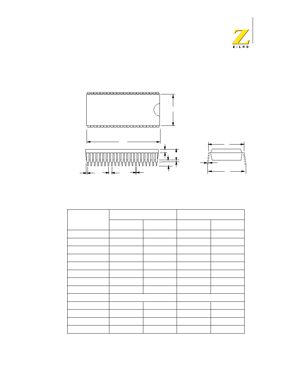
Z90255 ROM and Z90251 OTP
32 KB Television Controller with OSD
PS001301-0800
87
12
Packaging
Figure 23 42-Lead Shrink Dual-in-line Package (SDIP)
Table 75 Package Dimensions
Symbol
Millimeter
Inch
Min
Max
Min
Max
A1
0.51
.020
A2
4.32
.170
B
0.38
0.56
.015
.022
B1
0.76
1.27
.030
.050
C
0.20
0.30
.008
.012
D
36.70
36.96
1.445
1.455
E
15.24
15.88
.600
.625
E1
13.72
14.22
.540
.560
F
1.78 TYP
.070 TYP
eA
15.49
16.76
.610
.660
L
3.05
3.43
.120
.135
Q1
1.65
1.91
.065
.075
S
0.51
0.76
.020
.030
D
E1
1
21
22
42
E
eA
C
B
S
Q1
L
A2
A1
F

Z90255 ROM and Z90251 OTP
32 KB Television Controller with OSD
PS001301-0800
88
Ordering Information
ROM Code Submission
ROM Code Submission Instructions
ROM Code can be submitted on ZiLOG’s web site at http://www.zilog.com.
Top Mark Information
Mark Permanency: 3X soak into Alpha 2110 at 63
∞
to 70
∞
C, for 30 seconds
duration each soak. Mechanical brush after each soak.
Part
PSI
Description
Z90251
Z9025106PSC
OTP TV Controller
Z90255
Z9025506PSC Rxxxx*
Masked ROM TV Controller
Z9025900ZEM
Z9025900ZEM
Emulator/Programmer
Z9020900TSC
Z9020900TSC
Protopak
Note: * xxxx is a unique ROM number assigned to each customer code

Z90255 ROM and Z90251 OTP
32 KB Television Controller with OSD
PS001301-0800
89
Customer Feedback Form
Z90255 Product Specification
I
f there are any problems while operating this product, or any inaccuracies in the
specification, please copy and complete this form, then mail or fax it to ZiLOG.
Suggestions welcome!
Customer Information
Product Information
Return Information
ZiLOG
System Test/Customer Support
910 E. Hamilton Avenue, Suite 110, MS 4–3
Campbell, CA 95008
Fax: (408) 558-8536 Email: tools@zilog.com
Problem Description or Suggestion
Provide a complete description of the problem or suggestion. For specific problems,
include all steps leading up to the occurrence of the problem. Attach additional pages as
necessary.
Name
Country
Company
Phone
Address
Fax
City/State/Zip
E-Mail
Serial # or Board Fab #/Rev. #
Software Version
Document Number
Host Computer Description/Type