 | –≠–ª–µ–∫—Ç—Ä–æ–Ω–Ω—ã–π –∫–æ–º–ø–æ–Ω–µ–Ω—Ç: Z90341 | –°–∫–∞—á–∞—Ç—å:  PDF PDF  ZIP ZIP |

1
Z90341
P R E L I M I N A R Y
CP97TEL2500
Zilog
Z90341
DIGITAL TELEVISION CONTROLLER
FEATURES
s
Part
OTP
RAM
Speed
Number
ROM
(Word)
(MHz)
Z90341
64K x 16
1K x 16
12
s
52-Pin Shrink DIP Package
s
4.5- to 5.5-Volt Operating Range
s
Z89C00 RISC Processor Core
s
0
∞
C to +70
∞
C Temperature Range
s
Direct Closed Caption Decoding
s
TV Tuner Serial Interface
s
Customized Character Set
s
Character Control Mode
s
Directly Controlled Receiver Functions
s
V-Chip Decode
The Z90341 is a member of Zilog's family of Digital
Television Controllers designed to provide complete audio
and video control of television receivers, video recorders,
and advanced on-screen display facilities.
The Z90341 features a powerful Z89C00 RISC processor
core that controls on-board peripheral functions and
registers using the standard processor instruction set.
In closed caption mode, text can be decoded directly from
the composite video signal and displayed on the screen
with assistance from the processor's digital signal
processing capabilities. The character representation in
this mode allows for a simple attribute control through the
insertion of control characters.
The character control mode provides access to the full set
of attribute controls. The modification of attributes is allowed
on a character-by-character basis. The insertion of control
characters permits direction of other character attributes.
Display attributes, including underlining, italics, blinking,
eight foreground/background colors, character position
offset delay, and background transparency, are made
possible through a fully customized 512 character set.
GENERAL DESCRIPTION
Serial interfacing with the television tuner is provided
through the tuner serial port. Digital channel tuning
adjustments may be accessed through the industry-
standard I
2
C port.
Additional hardware provides the capability to display two
to three times normal size characters. The smoothing logic
contained in the on-screen display circuit improves the
appearance of larger fonts. Special circuitry can be
activated to improve the visibility of text by adding a right-
sided shadow effect to the characters.
Receiver functions such as color and volume can be
directly controlled by six 8-bit pulse width modulated
ports.
Notes:
All Signals with a preceding front slash, "/", are active Low, e.g.:
B//W (WORD is active Low); /B/W (BYTE is active Low, only).
Power connections follow conventional descriptions below:
Connection
Circuit
Device
Power
V
CC
V
DD
Ground
GND
V
SS
P
RELIMINARY
C
USTOMER
P
ROCUREMENT
S
PECIFICATION
2
Z90341
P R E L I M I N A R Y
CP97TEL2500
Zilog
GENERAL DESCRIPTION
(Continued)
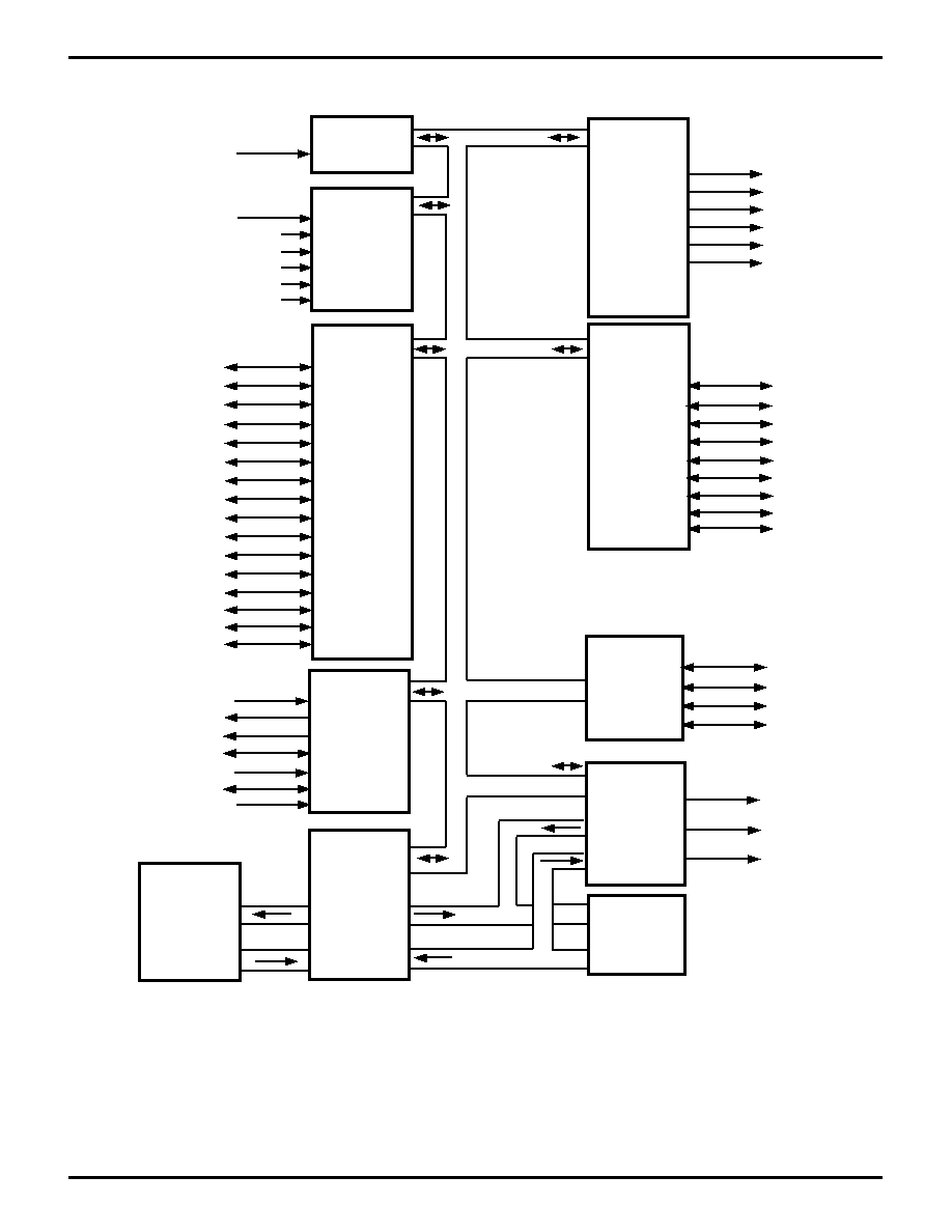
Functional Block Diagram
Capture
IRIN
ADC
ADC0
ADC1
ADC2
ADC3
ADC4
ADC5
Port 0
Port 00
Port 01
Port 02
Port 03
Port 04
Port 05
Port 06
Port 07
Port 08
Port 09
Control
XTAL1
XTAL2
LPF
HSYNC
VSYNC
/Reset
CPU
RAM
1K x 16
OSD
V1(R)
V2(G)
V3(B)
PWM
PWM1
PWM2
PWM3
PWM4
PWM5
PWM6
Port1
Port 10
Port 11
Port 12
Port 13
Port 14
Port 15
Port 16
Port 17
Port 00
Register Addr/Data
Address
Data
ROM Data
ROM Addr
CVI
Port 05
Port 04
Port 17
Port 18
I2C
SCL/MSCL2
SCD/MSCD2
MSCL1
MSCD1
Port 01/11
Port 02/12
HSYNC2
PWM6
Port 0A
Port 0B
Port 0C
Port 0D
Port 0E
Port 0F
OTP
ROM
64K X 16
3
Z90341
P R E L I M I N A R Y
CP97TEL2500
Zilog
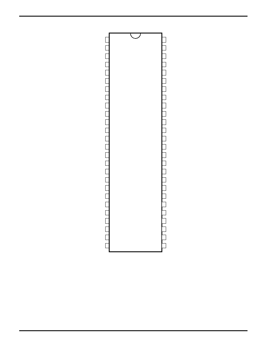
PIN DESCRIPTION
52-Pin Shrink DIP Configuration
1
2
9
3
4
5
6
7
8
52
51
50
49
48
47
46
45
44
43
42
41
40
39
14
10
11
12
13
15
16
17
18
19
20
38
37
36
35
34
33
Z90341
Port 16/SCLK
IRIN
Port 0C
Port 0B
Port 0A
Port 09
Port 0D
Port 07/CSync
Port 06/Counter
Port 03
Port 02/I2CSSC
Port 01/I2CSSD
CVI/ADC0
LPF
AGNDF
ADC5
Port 04/ADC4
Port 05/ADC3
Port 00/ADC2
Port 17/ADC1
Port15/B1
Port14/B0
Port13/G1
Port18/G0
Port08/R1
Port10/R0
PWM6/Hsync2
PWM5
PWM4
PWM3
PWM2
PWM1
AGNDX
VCC
GND
XTAL2
XTAL1
/Reset
I2MSC1
I2MSD1
AGND
AVCC
Port0F/Stransp
V3/B
V2/B
V1/B
21
22
23
24
25
26
32
31
30
29
28
27
Port 0E
Port11/I2CMSC2
Port12/I2CMSD2
VSync
HSync
Blank

4
Z90341
P R E L I M I N A R Y
CP97TEL2500
Zilog
PIN DESCRIPTION
Z89313
Pin
Z90341 Configuration
Name
Function
52-Pin
Direction
Reset
V
CC
, AV
CC
a
+5 V
39,22
PWR
≠
GND, AGND,
0 V
38,21,15,40
PWR
≠
AGNDF, AGNDX
b
IRIN
Infrared Remote Capture Input
2
I
I
ADC[5:1]
4-Bit Analog-to-Digital Converter
16,17,18,19,20
AI
I
Input
PWM[6:1]
8-Bit Pulse Width Modulator
46,45,44,43,42,41
O
O
Output
Port0[F:0]
Bit Programmable Input/Output Ports
23,32,7,3,4,5,6,48,8,9,18,
B
I
17,10,12,11,19
Port1[8:0]
Bit Programmable Input/Output Ports
49,20,1,52,51,50,30,
B
I
31,47
SCL
I
2
C Clock I/O
11,31,34
BOD
SCD
I
2
C Data I/O
12,30,33
BOD
XTAL1
Crystal Oscillator Input
36
AI
I
XTAL2
Crystal Oscillator Output
37
AO
O
LPF
Loop Filter
14
AB
O
HSYNC
H_Sync
28,46
B
I
VSYNC
V_Sync
29
B
I
/RESET
Device Reset
35
I
I
V[3:1]
OSD Video Output
24,25,26
O
O
(Typically Drive B, G, and R Outputs)
Blank
OSD Blank Output
27
O
O
Semi transparent
OSD Semi transparent Output
23
O
SCLK
Internal Processor SCLK
≠
O
Notes:
Please refer to pin-out diagram for shared pin numbers.
a) AV
CC
is for the reference voltage of the ADC input.
b) AGND is for the reference ground of the ADC input.
AGNDF is for LPF ground, and AGNDX is for XTAL circuit ground.
5
Z90341
P R E L I M I N A R Y
CP97TEL2500
Zilog
V1, V2, V3 ANALOG OUTPUT
Specifications V
CC
= 5.25 V
V
CC
= 5.25 V
Condition
Limit
Output Voltage
Bit = 11
2.10 V
±
0.3 V
Bit = 10
1.75 V
±
0.3 V
Bit = 01
1.28 V
±
0.30 V
Bit = 00
0.0 + 0.3V
Setting Time
70% of DC Level,
< 50 ns
10pf Load
V1, V2, V3 ANALOG OUTPUT
Specifications V
CC
= 4.75 V
V
CC
= 4.75 V
Condition
Limit
Output Voltage
Bit = 11
1.90 V
±
0.30 V
Bit = 10
1.60 V
±
0.30 V
Bit = 01
1.20 V
±
0.30 V
Bit = 00
0 V + 0.3 V
Setting Time
70% of DC Level,
< 50 ns
10pf Load
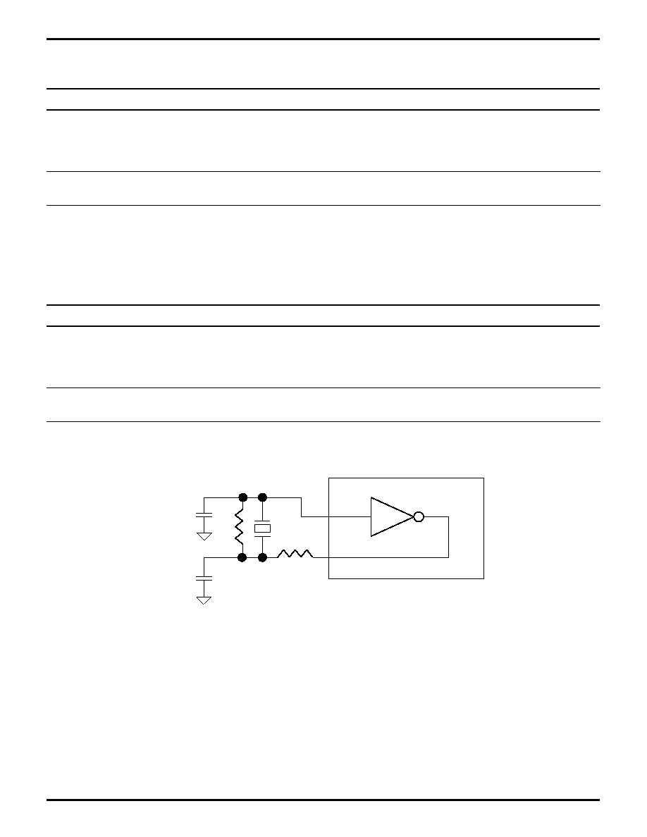
32K Oscillator Recommended Circuit
Z9034X
XTAL1
XTAL2
27k
560pF
68pF
10 Mohm
32.768k

6
Z90341
P R E L I M I N A R Y
CP97TEL2500
Zilog
ABSOLUTE MAXIMUM RATINGS
Symbol
Parameter
Min
Max
Units
Conditions
V
CC
Power Supply Voltage
0
7
V
V
ID
Input Voltage
≠0.3
V
CC
+0.3
V
Digital Inputs
V
IA
Input Voltage
≠0.3
V
CC
+0.3
V
Analog Inputs (A/D0...A/D4)
V
O
Output Voltage
≠0.3
V
CC
+0.3
V
All Push-Pull Digital Output
I
OH
Output Current High
≠10/≠1
a
mA
One Pin
I
OH
Output Current High
≠100
mA
All Pins
I
OL
Output Current Low
20/1
b
mA
One Pin
I
OL
Output Current Low
200
mA
All Pins
T
A
Operating Temperature
0
70
∞
C
T
S
Storage Temperature
≠65
150
∞
C
DC CHARACTERISTICS
T
A
= 0
∞
C to + 70
∞
C; V
CC
= 4.5 V to + 5.5 V; F
OSC
= 32.768 KHz
Symbol
Parameter
Min
Max
Typical
Units
Conditions
V
IL
Input Voltage Low
0
0.2 V
CC
0.4
V
V
IH
Input Voltage High
0.6 V
CC
V
CC
3.6
V
V
OL
Output Voltage Low
0.4
0.16
V
@ I
OL
= 1 mA
V
OH
Output Voltage High
V
CC
≠0.9
4.75
V
@ I
OL
= 0.75 mA
V
XL
Input Voltage XTAL1 Low
0.3 V
CC
1.0
V
External Clock
V
XH
Input Voltage XTAL1 High
V
CC
≠2.0
3.5
V
Generator Driven
V
HY
Schmitt Hysteresis
3.0
0.75
0.5
V
On XTAL1 Input Pin
I
IR
Reset Input Current
150
90
µ
A
V
RL
= 0 V
I
IL
Input Leakage
≠3.0
3.0
0.01
µ
A
@ 0 V and V
CC
I
CC
Supply Current
100
60
mA
I
CC1
Supply Current
300
100
µ
A
Sleep Mode @ 32 KHz
I
CC2
Supply Current
40
5
µ
A
Stop Mode
Notes:
a) 1 mA max. when output pad impedance is 600
.
b) 1 mA max. when output pad impedance is 600
.

7
Z90341
P R E L I M I N A R Y
CP97TEL2500
Zilog
AC CHARACTERISTICS
T
A
= 0
∞
C to + 70
∞
C; V
CC
= 4.5 V to 5.5 V; F
OSC
= 32.768 KHz
Symbol
Parameter
Min
Max
Typical
Units
Note
T
P
C
Input Clock Period
16
100
32
µ
s
T
R
C,T
F
C
Clock Input Rise and Fall
12
µ
s
T
D
POR
Power On Reset Delay
0.8
1.2
s
Depends on Crystal
AC CHARACTERISTICS*
T
A
= 0
∞
C to + 70
∞
C; V
CC
= 4.5 V to 5.5 V; F
OSC
= 32.768 KHz
Symbol
Parameter
Min
Max
Typical
Units
T
W
RES
Power-On Reset Min. Width
5TPC
µ
s
T
D
H
S
H_Sync Incoming Signal Width
5.5
12.5
11
µ
S
T
D
V
S
V_Sync Incoming Signal Width
0.15
1.5
1.0
ms
T
D
E
S
Time Delay Between Leading Edge
≠12
+12
0
µ
s
of V_Sync and H_Sync in Even Field
T
D
O
S
Time Delay Between Leading Edge
20
44
32
µ
s
of H_Sync in Odd Field
T
W
HV
S
H_Sync/V_Sync Edge Width
2.0
0.5
µ
s
Notes:
All timing of the I
2
C bus interface are defined by related specifications of
the I
2
C bus interface.
Zilog's products are not authorized for use as critical compo-
nents in life support devices or systems unless a specific written
agreement pertaining to such intended use is executed between
the customer and Zilog prior to use. Life support devices or
systems are those which are intended for surgical implantation
into the body, or which sustains life whose failure to perform,
when properly used in accordance with instructions for use
provided in the labeling, can be reasonably expected to result in
significant injury to the user.
Zilog, Inc. 210 East Hacienda Ave.
Campbell, CA 95008-6600
Telephone (408) 370-8000
Telex 910-338-7621
FAX 408 370-8056
Internet: http://www.zilog.com
© 1997 by Zilog, Inc. All rights reserved. No part of this document
may be copied or reproduced in any form or by any means
without the prior written consent of Zilog, Inc. The information in
this document is subject to change without notice. Devices sold
by Zilog, Inc. are covered by warranty and patent indemnification
provisions appearing in Zilog, Inc. Terms and Conditions of Sale
only. Zilog, Inc. makes no warranty, express, statutory, implied or
by description, regarding the information set forth herein or
regarding the freedom of the described devices from intellectual
property infringement. Zilog, Inc. makes no warranty of mer-
chantability or fitness for any purpose. Zilog, Inc. shall not be
responsible for any errors that may appear in this document.
Zilog, Inc. makes no commitment to update or keep current the
information contained in this document.