
ZiLOG Worldwide Headquarters ∑ 532 Race Street ∑ San Jose, CA 95126-3432
Telephone: 408.558.8500 ∑ Fax: 408.558.8300 ∑
www.ZiLOG.com
Preliminary Product Specification
PS023702-1004
Z8 GP
TM
Microcontrollers
ZGP323L
OTP MCU Family

Disclaimer
P r e l i m i n a r y
PS023702-1004
This publication is subject to replacement by a later edition. To determine whether a later edition
exists, or to request copies of publications, contact:
ZiLOG Worldwide Headquarters
532 Race Street
San Jose, CA 95126-3432
Telephone: 408.558.8500
Fax: 408.558.8300
www.
zilog
.com
ZiLOG is a registered trademark of ZiLOG Inc. in the United States and in other countries. All other products and/or
service names mentioned herein may be trademarks of the companies with which they are associated.
Document Disclaimer
©2004 by ZiLOG, Inc. All rights reserved. Information in this publication concerning the devices, applications, or
technology described is intended to suggest possible uses and may be superseded. ZiLOG, INC. DOES NOT
ASSUME LIABILITY FOR OR PROVIDE A REPRESENTATION OF ACCURACY OF THE INFORMATION, DEVICES,
OR TECHNOLOGY DESCRIBED IN THIS DOCUMENT. ZiLOG ALSO DOES NOT ASSUME LIABILITY FOR
INTELLECTUAL PROPERTY INFRINGEMENT RELATED IN ANY MANNER TO USE OF INFORMATION, DEVICES,
OR TECHNOLOGY DESCRIBED HEREIN OR OTHERWISE. Devices sold by ZiLOG, Inc. are covered by warranty
and limitation of liability provisions appearing in the ZiLOG, Inc. Terms and Conditions of Sale. ZiLOG, Inc. makes no
warranty of merchantability or fitness for any purpose. Except with the express written approval of ZiLOG, use of
information, devices, or technology as critical components of life support systems is not authorized. No licenses are
conveyed, implicitly or otherwise, by this document under any intellectual property rights.

Z8 GP
TM
OTP MCU Family
Product Specification
PS023702-1004
P r e l i m i n a r y
Table of Contents
iii
Table of Contents
Development Features . . . . . . . . . . . . . . . . . . . . . . . . . . . . . . . . . . . . . . . . . . . . 1
General Description . . . . . . . . . . . . . . . . . . . . . . . . . . . . . . . . . . . . . . . . . . . . . . . 2
Pin Description . . . . . . . . . . . . . . . . . . . . . . . . . . . . . . . . . . . . . . . . . . . . . . . . . . 4
Absolute Maximum Ratings . . . . . . . . . . . . . . . . . . . . . . . . . . . . . . . . . . . . . . . . 10
Standard Test Conditions . . . . . . . . . . . . . . . . . . . . . . . . . . . . . . . . . . . . . . . . . 10
DC Characteristics . . . . . . . . . . . . . . . . . . . . . . . . . . . . . . . . . . . . . . . . . . . . . . 11
AC Characteristics . . . . . . . . . . . . . . . . . . . . . . . . . . . . . . . . . . . . . . . . . . . . . . . 14
Pin Functions . . . . . . . . . . . . . . . . . . . . . . . . . . . . . . . . . . . . . . . . . . . . . . . . . . . 16
XTAL1 Crystal 1 (Time-Based Input) . . . . . . . . . . . . . . . . . . . . . . . . . . . . . 16
XTAL2 Crystal 2 (Time-Based Output) . . . . . . . . . . . . . . . . . . . . . . . . . . . . 16
Port 0 (P07≠P00) . . . . . . . . . . . . . . . . . . . . . . . . . . . . . . . . . . . . . . . . . . . . . 16
Port 1 (P17≠P10) . . . . . . . . . . . . . . . . . . . . . . . . . . . . . . . . . . . . . . . . . . . . . 17
Port 2 (P27≠P20) . . . . . . . . . . . . . . . . . . . . . . . . . . . . . . . . . . . . . . . . . . . . . 18
Port 3 (P37≠P30) . . . . . . . . . . . . . . . . . . . . . . . . . . . . . . . . . . . . . . . . . . . . . 19
RESET (Input, Active Low) . . . . . . . . . . . . . . . . . . . . . . . . . . . . . . . . . . . . . 23
Functional Description . . . . . . . . . . . . . . . . . . . . . . . . . . . . . . . . . . . . . . . . . . . . 23
Program Memory . . . . . . . . . . . . . . . . . . . . . . . . . . . . . . . . . . . . . . . . . . . . . 23
RAM . . . . . . . . . . . . . . . . . . . . . . . . . . . . . . . . . . . . . . . . . . . . . . . . . . . . . . 23
Expanded Register File . . . . . . . . . . . . . . . . . . . . . . . . . . . . . . . . . . . . . . . . 24
Register File . . . . . . . . . . . . . . . . . . . . . . . . . . . . . . . . . . . . . . . . . . . . . . . . 28
Stack . . . . . . . . . . . . . . . . . . . . . . . . . . . . . . . . . . . . . . . . . . . . . . . . . . . . . . 29
Timers . . . . . . . . . . . . . . . . . . . . . . . . . . . . . . . . . . . . . . . . . . . . . . . . . . . . . 30
Counter/Timer Functional Blocks . . . . . . . . . . . . . . . . . . . . . . . . . . . . . . . . 38
Expanded Register File Control Registers (0D) . . . . . . . . . . . . . . . . . . . . . . . . 64
Expanded Register File Control Registers (0F) . . . . . . . . . . . . . . . . . . . . . . . . . 69
Standard Control Registers . . . . . . . . . . . . . . . . . . . . . . . . . . . . . . . . . . . . . . . . 73
Package Information . . . . . . . . . . . . . . . . . . . . . . . . . . . . . . . . . . . . . . . . . . . . . 80
Ordering Information . . . . . . . . . . . . . . . . . . . . . . . . . . . . . . . . . . . . . . . . . . . . . 89
Precharacterization Product . . . . . . . . . . . . . . . . . . . . . . . . . . . . . . . . . . . . . . . 95

Z8 GP
TM
OTP MCU Family
Product Specification
PS023702-1004
P r e l i m i n a r y
iv
List of Figures
Figure 1. Functional Block Diagram . . . . . . . . . . . . . . . . . . . . . . . . . . . . . . . . . 3
Figure 2. Counter/Timers Diagram . . . . . . . . . . . . . . . . . . . . . . . . . . . . . . . . . . 4
Figure 3. 20-Pin PDIP/SOIC/SSOP/CDIP* Pin Configuration . . . . . . . . . . . . . . 5
Figure 4. 28-Pin PDIP/SOIC/SSOP/CDIP* Pin Configuration . . . . . . . . . . . . . . 6
Figure 5. 40-Pin PDIP/CDIP* Pin Configuration . . . . . . . . . . . . . . . . . . . . . . . . 7
Figure 6. 48-Pin SSOP Pin Configuration . . . . . . . . . . . . . . . . . . . . . . . . . . . . . 8
Figure 7. Test Load Diagram . . . . . . . . . . . . . . . . . . . . . . . . . . . . . . . . . . . . . 10
Figure 8. AC Timing Diagram . . . . . . . . . . . . . . . . . . . . . . . . . . . . . . . . . . . . . 14
Figure 9. Port 0 Configuration . . . . . . . . . . . . . . . . . . . . . . . . . . . . . . . . . . . . . 17
Figure 10. Port 1 Configuration . . . . . . . . . . . . . . . . . . . . . . . . . . . . . . . . . . . . . 18
Figure 11. Port 2 Configuration . . . . . . . . . . . . . . . . . . . . . . . . . . . . . . . . . . . . . 19
Figure 12. Port 3 Configuration . . . . . . . . . . . . . . . . . . . . . . . . . . . . . . . . . . . . . 20
Figure 13. Port 3 Counter/Timer Output Configuration . . . . . . . . . . . . . . . . . . . 22
Figure 14. Program Memory Map (32K OTP) . . . . . . . . . . . . . . . . . . . . . . . . . . 24
Figure 15. Expanded Register File Architecture . . . . . . . . . . . . . . . . . . . . . . . . 26
Figure 16. Register Pointer . . . . . . . . . . . . . . . . . . . . . . . . . . . . . . . . . . . . . . . . 27
Figure 17. Register Pointer--Detail . . . . . . . . . . . . . . . . . . . . . . . . . . . . . . . . . 29
Figure 18. Glitch Filter Circuitry . . . . . . . . . . . . . . . . . . . . . . . . . . . . . . . . . . . . 38
Figure 19. Transmit Mode Flowchart . . . . . . . . . . . . . . . . . . . . . . . . . . . . . . . . 39
Figure 20. 8-Bit Counter/Timer Circuits . . . . . . . . . . . . . . . . . . . . . . . . . . . . . . 40
Figure 21. T8_OUT in Single-Pass Mode . . . . . . . . . . . . . . . . . . . . . . . . . . . . . 41
Figure 22. T8_OUT in Modulo-N Mode . . . . . . . . . . . . . . . . . . . . . . . . . . . . . . 41
Figure 23. Demodulation Mode Count Capture Flowchart . . . . . . . . . . . . . . . . 42
Figure 24. Demodulation Mode Flowchart . . . . . . . . . . . . . . . . . . . . . . . . . . . . 43
Figure 25. 16-Bit Counter/Timer Circuits . . . . . . . . . . . . . . . . . . . . . . . . . . . . . 44
Figure 26. T16_OUT in Single-Pass Mode . . . . . . . . . . . . . . . . . . . . . . . . . . . . 45
Figure 27. T16_OUT in Modulo-N Mode . . . . . . . . . . . . . . . . . . . . . . . . . . . . . 45
Figure 28. Ping-Pong Mode Diagram . . . . . . . . . . . . . . . . . . . . . . . . . . . . . . . . 47
Figure 29. Output Circuit . . . . . . . . . . . . . . . . . . . . . . . . . . . . . . . . . . . . . . . . . . 47
Figure 30. Interrupt Block Diagram . . . . . . . . . . . . . . . . . . . . . . . . . . . . . . . . . . 49
Figure 31. Oscillator Configuration . . . . . . . . . . . . . . . . . . . . . . . . . . . . . . . . . . 51
Figure 32. Port Configuration Register (PCON) (Write Only) . . . . . . . . . . . . . . 53
Figure 33. STOP Mode Recovery Register . . . . . . . . . . . . . . . . . . . . . . . . . . . 55
Figure 34. SCLK Circuit . . . . . . . . . . . . . . . . . . . . . . . . . . . . . . . . . . . . . . . . . . 56

Z8 GP
TM
OTP MCU Family
Product Specification
PS023702-1004
P r e l i m i n a r y
v
Figure 35. Stop Mode Recovery Source . . . . . . . . . . . . . . . . . . . . . . . . . . . . . . 57
Figure 36. Stop Mode Recovery Register 2 ((0F)DH:D2≠D4, D6 Write Only) . 59
Figure 37. Watch-Dog Timer Mode Register (Write Only) . . . . . . . . . . . . . . . . 60
Figure 38. Resets and WDT . . . . . . . . . . . . . . . . . . . . . . . . . . . . . . . . . . . . . . . 61
Figure 39. TC8 Control Register ((0D)O0H: Read/Write Except Where Noted) 64
Figure 40. T8 and T16 Common Control Functions ((0D)01H: Read/Write) . . . 65
Figure 41. T16 Control Register ((0D) 2H: Read/Write Except Where Noted) . 67
Figure 42. T8/T16 Control Register (0D)03H: Read/Write
(Except Where Noted) . . . . . . . . . . . . . . . . . . . . . . . . . . . . . . . . . . . 68
Figure 43. Voltage Detection Register . . . . . . . . . . . . . . . . . . . . . . . . . . . . . . . 69
Figure 44. Port Configuration Register (PCON)(0F)00H: Write Only) . . . . . . . 70
Figure 45. Stop Mode Recovery Register ((0F)0BH: D6≠D0=Write Only,
D7=Read Only) . . . . . . . . . . . . . . . . . . . . . . . . . . . . . . . . . . . . . . . . 71
Figure 46. Stop Mode Recovery Register 2 ((0F)0DH:D2≠D4, D6 Write Only) 72
Figure 47. Watch-Dog Timer Register ((0F) 0FH: Write Only) . . . . . . . . . . . . . 73
Figure 48. Port 2 Mode Register (F6H: Write Only) . . . . . . . . . . . . . . . . . . . . . 73
Figure 49. Port 3 Mode Register (F7H: Write Only) . . . . . . . . . . . . . . . . . . . . . 74
Figure 50. Port 0 and 1 Mode Register (F8H: Write Only) . . . . . . . . . . . . . . . . 75
Figure 51. Interrupt Priority Register (F9H: Write Only) . . . . . . . . . . . . . . . . . . 76
Figure 52. Interrupt Request Register (FAH: Read/Write) . . . . . . . . . . . . . . . . 77
Figure 53. Interrupt Mask Register (FBH: Read/Write) . . . . . . . . . . . . . . . . . . . 77
Figure 54. Flag Register (FCH: Read/Write) . . . . . . . . . . . . . . . . . . . . . . . . . . . 78
Figure 55. Register Pointer (FDH: Read/Write) . . . . . . . . . . . . . . . . . . . . . . . . 78
Figure 56. Stack Pointer High (FEH: Read/Write) . . . . . . . . . . . . . . . . . . . . . . 79
Figure 57. Stack Pointer Low (FFH: Read/Write) . . . . . . . . . . . . . . . . . . . . . . . 79
Figure 58. 20-Pin CDIP Package . . . . . . . . . . . . . . . . . . . . . . . . . . . . . . . . . . . 80
Figure 59. 20-Pin PDIP Package Diagram . . . . . . . . . . . . . . . . . . . . . . . . . . . . 81
Figure 60. 20-Pin SOIC Package Diagram . . . . . . . . . . . . . . . . . . . . . . . . . . . . 81
Figure 61. 20-Pin SSOP Package Diagram . . . . . . . . . . . . . . . . . . . . . . . . . . . 82
Figure 62. 28-Pin CDIP Package . . . . . . . . . . . . . . . . . . . . . . . . . . . . . . . . . . . 83
Figure 63. 28-Pin SOIC Package Diagram . . . . . . . . . . . . . . . . . . . . . . . . . . . . 84
Figure 64. 28-Pin PDIP Package Diagram . . . . . . . . . . . . . . . . . . . . . . . . . . . . 85
Figure 65. 28-Pin SSOP Package Diagram . . . . . . . . . . . . . . . . . . . . . . . . . . . 86
Figure 66. 40-Pin CDIP Package . . . . . . . . . . . . . . . . . . . . . . . . . . . . . . . . . . . 87
Figure 67. 40-Pin PDIP Package Diagram . . . . . . . . . . . . . . . . . . . . . . . . . . . . 87
Figure 68. 48-Pin SSOP Package Design . . . . . . . . . . . . . . . . . . . . . . . . . . . . 88

Z8 GP
TM
OTP MCU Family
Product Specification
PS023702-1004
P r e l i m i n a r y
vi
List of Tables
Table 1.
Features . . . . . . . . . . . . . . . . . . . . . . . . . . . . . . . . . . . . . . . . . . . . . . 1
Table 2.
Power Connections . . . . . . . . . . . . . . . . . . . . . . . . . . . . . . . . . . . . . . 3
Table 3.
20-Pin PDIP/SOIC/SSOP/CDIP* Pin Identification. . . . . . . . . . . . . . . 5
Table 4.
28-Pin PDIP/SOIC/SSOP/CDIP* Pin Identification. . . . . . . . . . . . . . . 6
Table 5.
40- and 48-Pin Configuration . . . . . . . . . . . . . . . . . . . . . . . . . . . . . . . 8
Table 6.
Absolute Maximum Ratings . . . . . . . . . . . . . . . . . . . . . . . . . . . . . . . 10
Table 7.
Capacitance . . . . . . . . . . . . . . . . . . . . . . . . . . . . . . . . . . . . . . . . . . . 11
Table 8.
DC Characteristics . . . . . . . . . . . . . . . . . . . . . . . . . . . . . . . . . . . . . . 11
Table 9.
EPROM/OTP Characteristics . . . . . . . . . . . . . . . . . . . . . . . . . . . . . 13
Table 10. AC Characteristics . . . . . . . . . . . . . . . . . . . . . . . . . . . . . . . . . . . . . . 15
Table 11. Port 3 Pin Function Summary . . . . . . . . . . . . . . . . . . . . . . . . . . . . . 21
Table 12. CTR0(D)00H Counter/Timer8 Control Register . . . . . . . . . . . . . . . . 31
Table 13. CTR1(0D)01H T8 and T16 Common Functions . . . . . . . . . . . . . . . . 33
Table 14. CTR2(D)02H: Counter/Timer16 Control Register. . . . . . . . . . . . . . . 36
Table 15. CTR3 (D)03H: T8/T16 Control Register . . . . . . . . . . . . . . . . . . . . . 37
Table 16. Interrupt Types, Sources, and Vectors . . . . . . . . . . . . . . . . . . . . . . . 50
Table 17. IRQ Register . . . . . . . . . . . . . . . . . . . . . . . . . . . . . . . . . . . . . . . . . . 50
Table 18. SMR2(F)0DH:Stop Mode Recovery Register 2* . . . . . . . . . . . . . . . 56
Table 19. Stop Mode Recovery Source . . . . . . . . . . . . . . . . . . . . . . . . . . . . . . 58
Table 20. Watch-Dog Timer Time Select . . . . . . . . . . . . . . . . . . . . . . . . . . . . . 61
Table 21. EPROM Selectable Options . . . . . . . . . . . . . . . . . . . . . . . . . . . . . . 62

Z8 GP
TM
OTP MCU Family
Product Specification
PS023702-1004
P r e l i m i n a r y Development
Features
1
Development Features
Table 1 lists the features of ZiLOG
Æ
's Z8 GP
TM
OTP MCU Family family mem-
bers.
∑
Low power consumption≠6mW (typical)
∑
T = Temperature
S = Standard 0∞ to +70∞C
E = Extended -40∞ to +105∞C
A = Automotive -40∞ to +125∞C
∑
Three standby modes:
≠ STOP--2
µ
A (typical)
≠ HALT--0.8mA (typical)
≠ Low voltage reset
∑
Special architecture to automate both generation and reception of complex pulses
or signals:
≠ One programmable 8-bit counter/timer with two capture registers and two
load registers
≠ One programmable 16-bit counter/timer with one 16-bit capture register
pair and one 16-bit load register pair
≠ Programmable input glitch filter for pulse reception
∑
Six priority interrupts
≠ Three external
≠ Two assigned to counter/timers
≠ One low-voltage detection interrupt
∑
Low voltage detection and high voltage detection flags
∑
Programmable Watch-Dog Timer/Power-On Reset (WDT/POR) circuits
∑
Two independent comparators with programmable interrupt polarity
∑
Programmable EPROM options
≠ Port 0: 0≠3 pull-up transistors
≠ Port 0: 4≠7 pull-up transistors
Table 1. Features
Device
OTP (KB) RAM (Bytes)
I/O Lines Voltage Range
ZGP323L OTP MCU
Family
4, 8, 16, 32
237
32, 24 or 16
2.0V≠3.6V

Z8 GP
TM
OTP MCU Family
Product Specification
PS023702-1004
P r e l i m i n a r y General
Description
2
≠ Port 1: 0≠3 pull-up transistors
≠ Port 1: 4≠7 pull-up transistors
≠ Port 2: 0≠7 pull-up transistors
≠ EPROM Protection
≠ WDT enabled at POR
The mask option pull-up transistor has a typical equivalent
resistance of 200 K
±
50% at V
CC
=3 V and 450 K
±
50% at
V
CC
=2 V.
General Description
The Z8 GP
TM
OTP MCU Family is an OTP-based member of the MCU family of
infrared microcontrollers. With 237B of general-purpose RAM and up to 32KB of
OTP, ZiLOG
Æ
's CMOS microcontrollers offer fast-executing, efficient use of mem-
ory, sophisticated interrupts, input/output bit manipulation capabilities, automated
pulse generation/reception, and internal key-scan pull-up transistors.
The Z8 GP
TM
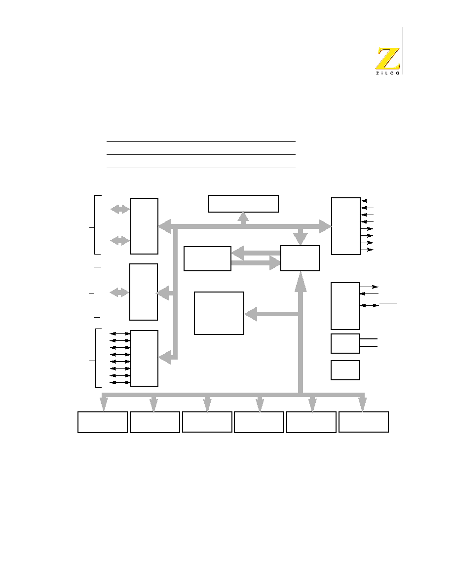
OTP MCU Family architecture (Figure 1) is based on ZiLOG's 8-bit
microcontroller core with an Expanded Register File allowing access to register-
mapped peripherals, input/output (I/O) circuits, and powerful counter/timer cir-
cuitry. The Z8
Æ
offers a flexible I/O scheme, an efficient register and address
space structure, and a number of ancillary features that are useful in many con-
sumer, automotive, computer peripheral, and battery-operated hand-held applica-
tions.
There are three basic address spaces available to support a wide range of config-
urations: Program Memory, Register File and Expanded Register File. The regis-
ter file is composed of 256 Bytes (B) of RAM. It includes 4 I/O port registers, 16
control and status registers, and 236 general-purpose registers. The Expanded
Register File consists of two additional register groups (F and D).
To unburden the program from coping with such real-time problems as generating
complex waveforms or receiving and demodulating complex waveform/pulses, the
Z8 GP OTP MCU offers a new intelligent counter/timer architecture with 8-bit and
16-bit counter/timers (see Figure 2). Also included are a large number of user-
selectable modes and two on-board comparators to process analog signals with
separate reference voltages.
All signals with an overline, " ", are active Low. For example,
B/W, in which WORD is active Low, and B/W, in which BYTE is
active Low.
Power connections use the conventional descriptions listed in Table 2.
Note:
Note:
Z8 GP
TM
OTP MCU Family
Product Specification
PS023702-1004
P r e l i m i n a r y General
Description
3
Figure 1. Functional Block Diagram
Table 2. Power Connections
Connection
Circuit
Device
Power
V
CC
V
DD
Ground
GND
V
SS
Z8Æ Core
Port 2
Port 0
P21
P22
P23
P24
P25
P26
P27
P20
I/O Bit
Programmable
P04
P05
P06
P07
P00
P01
P02
P03
I/O Nibble
Programmable
Register File
256 x 8-Bit
Register Bus
Internal
Address Bus
Internal
Data Bus
Expanded
Register
File
Expanded
Register Bus
Z8
Æ
Core
Counter/Timer 8
8-Bit
Counter/Timer 16
16-Bit
V
DD
V
SS
XTAL
RESET
Pref1/P30
P31
P32
P33
P34
P35
P36
P37
Port 3
Machine
Timing &
Instruction
Control
Power
4
4
OTP
Up to 32K x 8
Port 1
P14
P15
P16
P17
P10
P11
P12
P13
I/O Byte
Programmable
8
Watch-Dog
Timer
Low Voltage
Detection
High Voltage
Detection
2-Comparators
Note: Refer to the specific package for available pins.
Power-On
Reset

Z8 GP
TM
OTP MCU Family
Product Specification
PS023702-1004
P r e l i m i n a r y Pin
Description
4
Figure 2. Counter/Timers Diagram
Pin Description
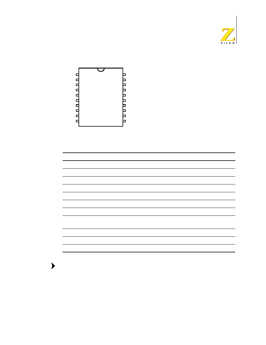
The pin configuration for the 20-pin PDIP/SOIC/SSOP is illustrated in Figure 3
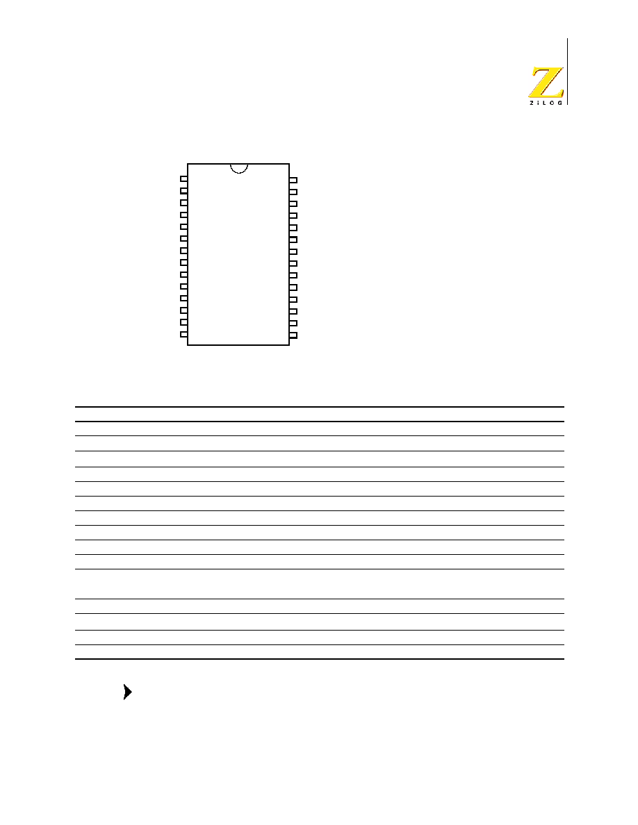
and described in Table 3. The pin configuration for the 28-pin PDIP/SOIC/SSOP
are depicted in Figure 4 and described in Table 4. The pin configurations for the
40-pin PDIP and 48-pin SSOP versions are illustrated in Figure 5, Figure 6, and
described in Table 5.
For customer engineering code development, a UV eraseable windowed cerdip
packaging is offered in 20-pin, 28-pin, and 40-pin configurations. ZiLOG does not
recommend nor guarantee these packages for use in production.
HI16
LO16
16-Bit
T16
TC16H
TC16L
HI8
LO8
And/Or
Logic
Clock
Divider
Glitch
Filter
Edge
Detect
Circuit
8-Bit
T8
TC8H
TC8L
8
8
16
8
Input
SCLK
1 2 4 8
Timer 16
Timer 8/16
Timer 8
8
8
8
8
8
Z8 GP
TM
OTP MCU Family
Product Specification
PS023702-1004
P r e l i m i n a r y Pin
Description
5
Figure 3. 20-Pin PDIP/SOIC/SSOP/CDIP* Pin Configuration
*Windowed Cerdip. These units are intended to be used for
engineering code development only. ZiLOG does not
recommend/guarantee this package for production use.
Table 3. 20-Pin PDIP/SOIC/SSOP/CDIP* Pin Identification
Pin #
Symbol
Function
Direction
1≠3
P25≠P27
Port 2, Bits 5,6,7
Input/Output
4
P07
Port 0, Bit 7
Input/Output
5
V
DD
Power Supply
6
XTAL2
Crystal Oscillator Clock
Output
7
XTAL1
Crystal Oscillator Clock
Input
8≠10
P31≠P33
Port 3, Bits 1,2,3
Input
11,12
P34. P36
Port 3, Bits 4,6
Output
13
P00/Pref1/P30 Port 0, Bit 0/Analog reference input
Port 3 Bit 0
Input/Output for P00
Input for Pref1/P30
14
P01
Port 0, Bit 1
Input/Output
15
V
SS
Ground
16≠20
P20≠P24
Port 2, Bits 0,1,2,3,4
Input/Output
P25
P26
P27
P07
V
DD
XTAL2
XTAL1
P31
P32
P33
P24
P23
P22
P21
P20
V
SS
P01
P00/Pref1/P30
P36
P34
1
2
3
4
5
6
7
8
9
10
20
19
18
17
16
15
14
13
12
11
20-Pin
PDIP
SOIC
SSOP
CDIP*
Note:
Z8 GP
TM
OTP MCU Family
Product Specification
PS023702-1004
P r e l i m i n a r y Pin
Description
6
Figure 4. 28-Pin PDIP/SOIC/SSOP/CDIP* Pin Configuration
*Windowed Cerdip. These units are intended to be used for
engineering code development only. ZiLOG does not
recommend/guarantee this package for production use.
Table 4. 28-Pin PDIP/SOIC/SSOP/CDIP* Pin Identification
Pin Symbol
Direction
Description
1-3
P25-P27
Input/Output
Port 2, Bits 5,6,7
4-7
P04-P07
Input/Output
Port 0, Bits 4,5,6,7
8
V
DD
Power supply
9
XTAL2
Output
Crystal, oscillator clock
10
XTAL1
Input
Crystal, oscillator clock
11-13
P31-P33
Input
Port 3, Bits 1,2,3
14
P34
Output
Port 3, Bit 4
15
P35
Output
Port 3, Bit 5
16
P37
Output
Port 3, Bit 7
17
P36
Output
Port 3, Bit 6
18
Pref1/P30
Port 3 Bit 0
Input
Analog ref input; connect to V
CC
if not used
Input for Pref1/P30
19-21
P00-P02
Input/Output
Port 0, Bits 0,1,2
22
V
SS
Ground
23
P03
Input/Output
Port 0, Bit 3
24-28
P20-P24
Input/Output
Port 2, Bits 0-4
P24
P23
P22
P21
P20
P03
V
SS
P02
P01
P00
Pref1/P30
P36
P37
P35
P25
P26
P27
P04
P05
P06
P07
V
DD
XTAL2
XTAL1
P31
P32
P33
P34
1
28-Pin
PDIP
SOIC
SSOP
2
3
4
5
6
7
8
9
10
11
12
13
14
28
27
26
25
24
23
22
21
20
19
18
17
16
15
CDIP*
Note:

Z8 GP
TM
OTP MCU Family
Product Specification
PS023702-1004
P r e l i m i n a r y Pin
Description
7
Figure 5. 40-Pin PDIP/CDIP* Pin Configuration
*Windowed Cerdip. These units are intended to be used for
engineering code development only. ZiLOG does not
recommend/guarantee this package for production use.
NC
P25
P26
P27
P04
P05
P06
P14
P15
P07
VDD
P16
P17
XTAL2
XTAL1
P31
P32
P33
P34
NC
NC
P24
P23
P22
P21
P20
P03
P13
P12
VSS
P02
P11
P10
P01
P00
Pref1/P30
P36
P37
P35
RESET
1
2
3
4
5
6
7
8
9
10
11
12
13
14
15
16
17
18
19
20
40
39
38
37
36
35
34
33
32
31
30
39
28
27
26
25
24
23
22
21
40-Pin
PDIP
CDIP*
Note:
Z8 GP
TM
OTP MCU Family
Product Specification
PS023702-1004
P r e l i m i n a r y Pin
Description
8
Figure 6. 48-Pin SSOP Pin Configuration
Table 5. 40- and 48-Pin Configuration
40-Pin PDIP/CDIP* # 48-Pin SSOP #
Symbol
26
31
P00
27
32
P01
30
35
P02
34
41
P03
5
5
P04
6
7
P05
7
8
P06
10
11
P07
28
33
P10
29
34
P11
32
39
P12
NC
P25
P26
P27
P04
N/C
P05
P06
P14
P15
P07
VDD
VDD
N/C
P16
P17
XTAL2
XTAL1
P31
P32
P33
P34
NC
VSS
NC
NC
P24
P23
P22
P21
P20
P03
P13
P12
VSS
VSS
N/C
P02
P11
P10
P01
P00
N/C
PREF1/P30
P36
P37
P35
RESET
48-Pin
SSOP
1
2
3
4
5
6
7
8
9
10
11
12
13
14
15
16
17
18
19
20
21
22
23
24
48
47
46
45
44
43
42
41
40
39
38
37
36
35
34
33
32
31
30
29
28
27
26
25

Z8 GP
TM
OTP MCU Family
Product Specification
PS023702-1004
P r e l i m i n a r y Pin
Description
9
33
40
P13
8
9
P14
9
10
P15
12
15
P16
13
16
P17
35
42
P20
36
43
P21
37
44
P22
38
45
P23
39
46
P24
2
2
P25
3
3
P26
4
4
P27
16
19
P31
17
20
P32
18
21
P33
19
22
P34
22
26
P35
24
28
P36
23
27
P37
20
23
NC
40
47
NC
1
1
NC
21
25
RESET
15
18
XTAL1
14
17
XTAL2
11
12, 13
V
DD
31
24, 37, 38
V
SS
25
29
Pref1/P30
48
NC
Table 5. 40- and 48-Pin Configuration (Continued)
40-Pin PDIP/CDIP* # 48-Pin SSOP #
Symbol

Z8 GP
TM
OTP MCU Family
Product Specification
PS023702-1004
P r e l i m i n a r y Absolute
Maximum
Ratings
10
Absolute Maximum Ratings
Stresses greater than those listed in Table 7 might cause permanent damage to
the device. This rating is a stress rating only. Functional operation of the device at
any condition above those indicated in the operational sections of these specifica-
tions is not implied. Exposure to absolute maximum rating conditions for an
extended period might affect device reliability.
Standard Test Conditions
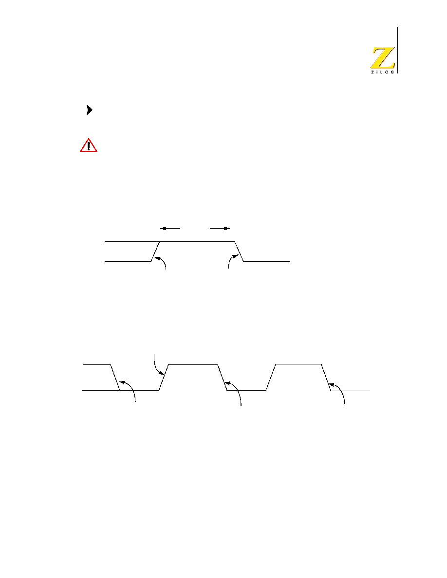
The characteristics listed in this product specification apply for standard test con-
ditions as noted. All voltages are referenced to GND. Positive current flows into
the referenced pin (see Figure 7).
Figure 7. Test Load Diagram
Table 6. Absolute Maximum Ratings
Parameter
Minimum Maximum Units
Notes
Ambient temperature under bias
0
+70
C
Storage temperature
≠65
+150
C
Voltage on any pin with respect to V
SS
≠0.3
+5.5
V
1
Voltage on V
DD
pin with respect to V
SS
≠0.3
+3.6
V
Maximum current on input and/or inactive output pin
≠5
+5
µA
Maximum output current from active output pin
≠25
+25
mA
Maximum current into V
DD
or out of V
SS
75
mA
Notes:
This voltage applies to all pins except the following: V
DD
, P32, P33 and RESET.
From Output
Under Test
150pF

Z8 GP
TM
OTP MCU Family
Product Specification
PS023702-1004
P r e l i m i n a r y DC
Characteristics
11
Capacitance
Table 7 lists the capacitances.
DC Characteristics
Table 7. Capacitance
Parameter
Maximum
Input capacitance
12pF
Output capacitance
12pF
I/O capacitance
12pF
Note: T
A
= 25∞ C, V
CC
= GND = 0 V, f = 1.0 MHz, unmeasured pins returned to GND
Table 8. DC Characteristics
T
A
= 0∞C to +70∞C
Units Conditions
Notes
Symbol Parameter
V
CC
Min
Typ Max
V
CC
Supply Voltage
2.0
3.6
V
See Note 5
5
V
CH
Clock Input High
Voltage
2.0-3.6
0.8
V
CC
+0.3 V
Driven by External
Clock Generator
V
CL
Clock Input Low
Voltage
2.0-3.6
VSS≠0.3
0.5
V
Driven by External
Clock Generator
V
IH
Input High Voltage
2.0-3.6
0.7 V
CC
V
CC
+0.3 V
V
IL
Input Low Voltage
2.0-3.6
V
SS
≠0.3
0.2 V
CC
V
V
OH1
Output High Voltage
2.0-3.6
V
CC
≠0.4
V
I
OH
= ≠0.5mA
V
OH2
Output High Voltage
(P36, P37, P00, P01)
2.0-3.6
V
CC
≠0.8
V
I
OH
= ≠7mA
V
OL1
Output Low Voltage
2.0-3.6
0.4
V
I
OL
= 1.0mA
I
OL
= 4.0mA
V
OL2
Output Low Voltage
(P00, P01, P36, P37)
2.0-3.6
0.8
V
I
OL
= 10mA
V
OFFSET
Comparator Input
Offset Voltage
2.0-3.6
25
mV
V
REF
Comparator
Reference
Voltage
2.0-3.6
0
V
DD
-1.75
V
IIL
Input Leakage
2.0-3.6
≠1
1
µ
A
VIN = 0V, VCC
Pull-ups disabled
IOL
Output Leakage
2.0-3.6
≠1
1
µ
A
VIN = 0V, VCC
ICC
Supply Current
2.0
3.6
10
15
mA
mA
at 8.0 MHz
at 8.0 MHz
1, 2
1, 2

Z8 GP
TM
OTP MCU Family
Product Specification
PS023702-1004
P r e l i m i n a r y DC
Characteristics
12
I
CC1
Standby Current
(HALT Mode)
2.0
3.6
2.0
3.6
3
5
2
4
mA
V
IN
= 0V, VCC at 8.0MHz
Same as above
Clock Divide-by-16 at 8.0MHz
Same as above
1, 2
1, 2
1, 2
1, 2
I
CC2
Standby Current (Stop
Mode)
2.0
3.6
2.0
3.6
8
10
500
800
µ
A
µ
A
µ
A
µ
A
VIN = 0 V, VCC WDT is not Running
Same as above
V
IN
= 0 V, V
CC
WDT is Running
Same as above
3
3
3
3
I
LV
Standby Current
(Low Voltage)
10
µ
A
Measured at 1.3V
4
V
BO
V
CC
Low Voltage
Protection
2.0
V
8MHz maximum
Ext. CLK Freq.
V
LVD
Vcc Low Voltage
Detection
2.4
V
V
HVD
Vcc High Voltage
Detection
2.7
V
Notes:
1. All outputs unloaded, inputs at rail.
2. CL1 = CL2 = 100 pF.
3. Oscillator stopped.
4. Oscillator stops when V
CC
falls below V
BO
limit.
5. It is strongly recommended to add a filter capacitor (minimum 0.1
µ
F), physically close to the V
DD
and V
SS
pins if oper-
ating voltage fluctuations are anticipated, such as those resulting from driving an Infrared LED.
Table 8. DC Characteristics (Continued)
T
A
= 0∞C to +70∞C
Units Conditions
Notes
Symbol Parameter
V
CC
Min
Typ Max

Z8 GP
TM
OTP MCU Family
Product Specification
PS023702-1004
P r e l i m i n a r y DC
Characteristics
13
Table 9. EPROM/OTP Characteristics
Symbol Parameter
Min.
Typ.
Max. Unit
Notes
Erase Time
15
Minutes
1,3
Data Retention @ use years
10
Years
2
Program/Erase Endurance
25
Cycles
1
Notes:
1. For windowed cerdip package only.
2. Standard: 0∞C to 70∞C; Extended: -40∞C to +105∞C; Automotive: -40∞C to +125∞C.
Determined using the Arrhenius model, which is an industry standard for estimating data
retention of floating gate technologies:
AF = exp[(Ea/k)*(1/Tuse - 1/TStress)]
Where:
Ea is the intrinsic activation energy (eV; typ. 0.8)
k is Boltzman's constant (8.67 x 10⁻⁵ eV/∞K)
∞K = -273.16∞C
Tuse = Use Temperature in ∞K
TStress = Stress Temperature in ∞K
3. At a stable UV Lamp output of 20mW/CM
2
Z8 GP
TM
OTP MCU Family
Product Specification
PS023702-1004
P r e l i m i n a r y AC
Characteristics
14
AC Characteristics
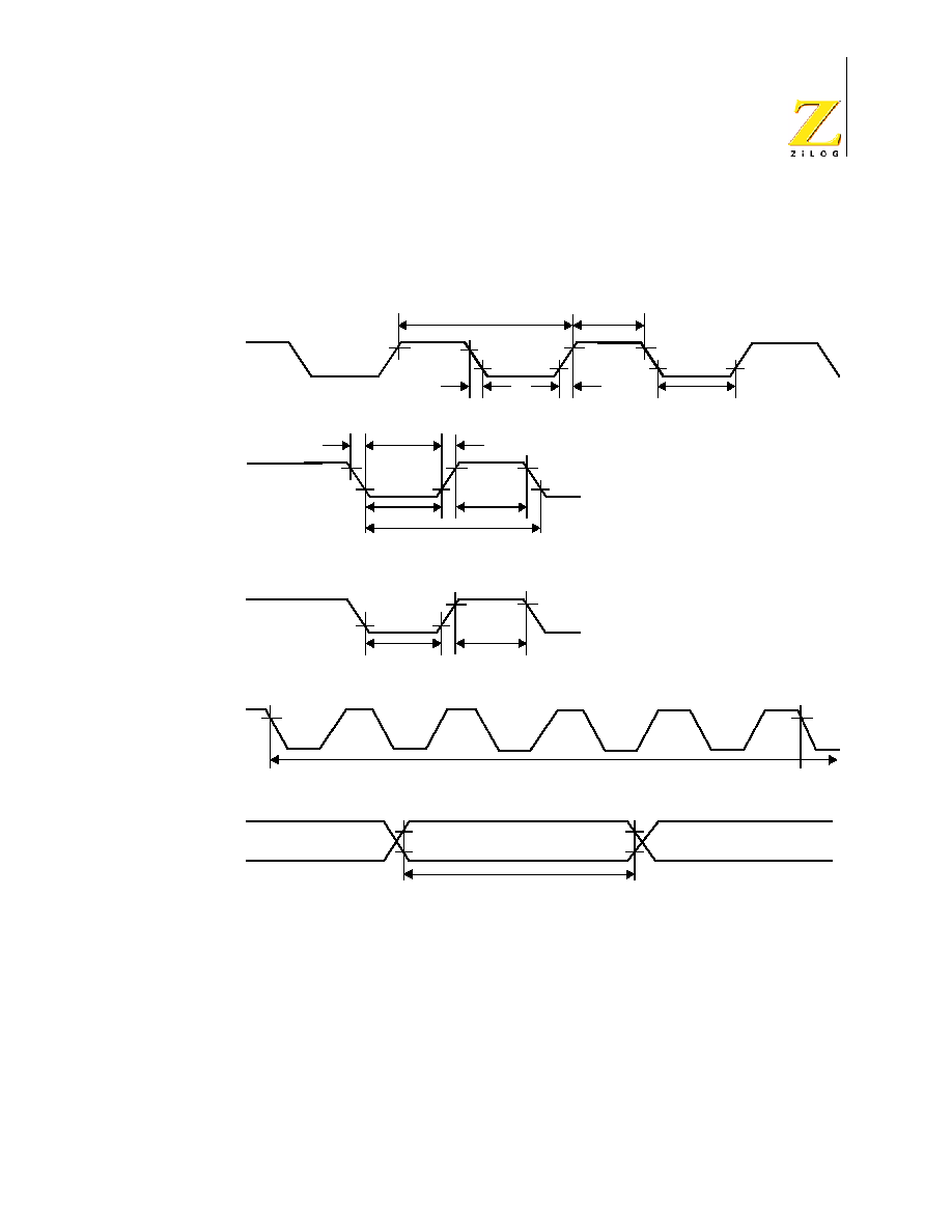
Figure 8 and Table 10 describe the Alternating Current (AC) characteristics.
Figure 8. AC Timing Diagram
Clock
Stop
Mode
Recovery
Source
Clock
Setup
1
2
2
3
3
T
IN
7
4
5
6
7
IRQ
N
8
9
11
10

Z8 GP
TM
OTP MCU Family
Product Specification
PS023702-1004
P r e l i m i n a r y AC
Characteristics
15
Table 10. AC Characteristics
T
A
=0∞C to +70∞C
8.0MHz
Watch-Dog
Timer
Mode
Register
(D1, D0)
No Symbol
Parameter
V
CC
Minimum
Maximum
Units Notes
1
TpC
Input Clock Period
2.0≠3.6
121
DC
ns
1
2
TrC,TfC
Clock Input Rise and
Fall Times
2.0≠3.6
25
ns
1
3
TwC
Input Clock Width
2.0≠3.6
37
ns
1
4
TwTinL
Timer Input
Low Width
2.0
3.6
100
70
ns
1
5
TwTinH
Timer Input High
Width
2.0≠3.6
3TpC
1
6
TpTin
Timer Input Period
2.0≠3.6
8TpC
1
7
TrTin,TfTin Timer Input Rise and
Fall Timers
2.0≠3.6
100
ns
1
8
TwIL
Interrupt Request
Low Time
2.0
3.6
100
70
ns
1, 2
9
TwIH
Interrupt Request
Input High Time
2.0≠3.6
5TpC
1, 2
10 Twsm
Stop-Mode
Recovery Width
Spec
2.0≠3.6
12
10TpC
ns
3
4
11 Tost
Oscillator
Start-Up Time
2.0≠3.6
5TpC
4
12 Twdt
Watch-Dog Timer
Delay Time
2.0≠3.6
2.0≠3.6
2.0≠3.6
2.0≠3.6
5
10
20
80
ms
ms
ms
ms
0, 0
0, 1
1, 0
1, 1
13 T
POR
Power-On Reset
2.0≠3.6
2.5
10
ms
Notes:
1. Timing Reference uses 0.9 V
CC
for a logic 1 and 0.1 V
CC
for a logic 0.
2. Interrupt request through Port 3 (P33≠P31).
3. SMR ≠ D5 = 1.
4. SMR ≠ D5 = 0.

Z8 GP
TM
OTP MCU Family
Product Specification
PS023702-1004
P r e l i m i n a r y Pin
Functions
16
Pin Functions
XTAL1 Crystal 1 (Time-Based Input)
This pin connects a parallel-resonant crystal or ceramic resonator to the on-chip
oscillator input. Additionally, an optional external single-phase clock can be coded
to the on-chip oscillator input.
XTAL2 Crystal 2 (Time-Based Output)
This pin connects a parallel-resonant crystal or ceramic resonant to the on-chip
oscillator output.
Port 0 (P07≠P00)
Port 0 is an 8-bit, bidirectional, CMOS-compatible port. These eight I/O lines are
configured under software control as a nibble I/O port. The output drivers are
push-pull or open-drain controlled by bit D2 in the PCON register.
If one or both nibbles are needed for I/O operation, they must be configured by
writing to the Port 0 mode register. After a hardware reset, Port 0 is configured as
an input port.
An optional pull-up transistor is available as a mask option on all Port 0 bits with
nibble select.
Internal pull-ups are disabled on any given pin or group of port
pins when programmed into output mode.
The Port 0 direction is reset to be input following an SMR.
Notes:
Z8 GP
TM
OTP MCU Family
Product Specification
PS023702-1004
P r e l i m i n a r y Pin
Functions
17
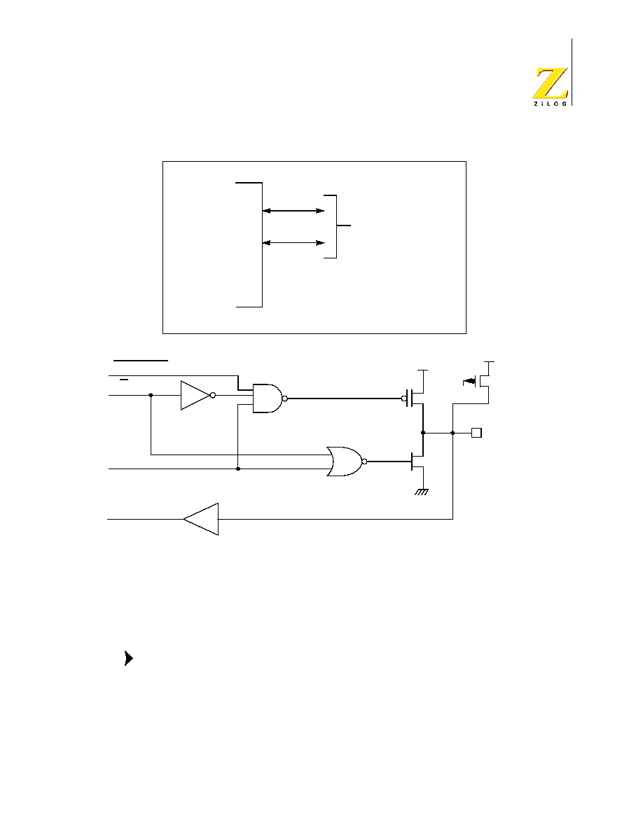
Figure 9. Port 0 Configuration
Port 1 (P17≠P10)
Port 1 (see Figure 10) Port 1 can be configured for standard port input or output
mode. After POR, Port 1 is configured as an input port. The output drivers are
either push-pull or open-drain and are controlled by bit D1 in the PCON register.
The Port 1 direction is reset to be input following an SMR.
OTP Programming
Option
4
4
Z8 GP
OTP
Port 0 (I/O)
Pad
In
Out
I/O
Open-Drain
Resistive
Transistor
Pull-up
V
CC
Note:
Z8 GP
TM
OTP MCU Family
Product Specification
PS023702-1004
P r e l i m i n a r y Pin
Functions
18
Figure 10. Port 1 Configuration
Port 2 (P27≠P20)
Port 2 is an 8-bit, bidirectional, CMOS-compatible I/O port (see Figure 11). These
eight I/O lines can be independently configured under software control as inputs
or outputs. Port 2 is always available for I/O operation. A mask option is available
to connect eight pull-up transistors on this port. Bits programmed as outputs are
globally programmed as either push-pull or open-drain. The POR resets with the
eight bits of Port 2 configured as inputs.
Port 2 also has an 8-bit input OR and AND gate, which can be used to wake up
the part. P20 can be programmed to access the edge-detection circuitry in
demodulation mode.
OTP Programming
Option
8
Z8 GP
OTP
Port 1 (I/O)
Pad
In
Out
OEN
Open-Drain
Resistive
Transistor
Pull-up
V
CC
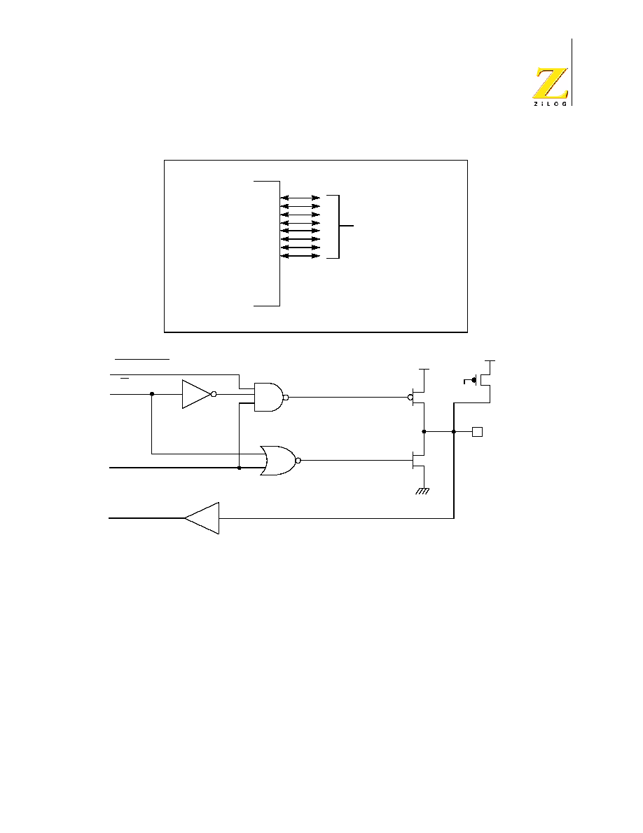
Z8 GP
TM
OTP MCU Family
Product Specification
PS023702-1004
P r e l i m i n a r y Pin
Functions
19
Figure 11. Port 2 Configuration
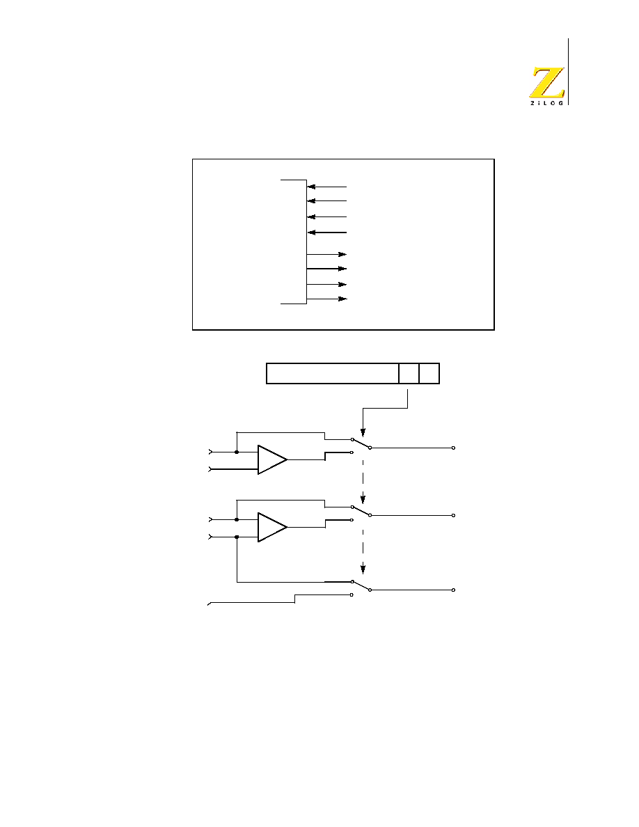
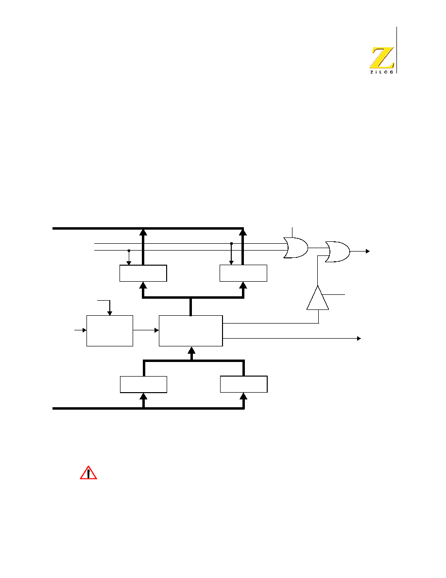
Port 3 (P37≠P30)
Port 3 is a 8-bit, CMOS-compatible fixed I/O port (see Figure 12). Port 3 consists
of four fixed input (P33≠P30) and four fixed output (P37≠P34), which can be con-
figured under software control for interrupt and as output from the counter/timers.
P30, P31, P32, and P33 are standard CMOS inputs; P34, P35, P36, and P37 are
push-pull outputs.
OTP Programming
Option
Z8 GP
OTP
Port 2 (I/O)
Pad
In
Out
I/O
Open-Drain
Resistive
Transistor
Pull-up
V
CC
Z8 GP
TM
OTP MCU Family
Product Specification
PS023702-1004
P r e l i m i n a r y Pin
Functions
20
Figure 12. Port 3 Configuration
Two on-board comparators process analog signals on P31 and P32, with refer-
ence to the voltage on Pref1 and P33. The analog function is enabled by program-
ming the Port 3 Mode Register (bit 1). P31 and P32 are programmable as rising,
falling, or both edge triggered interrupts (IRQ register bits 6 and 7). Pref1 and P33
are the comparator reference voltage inputs. Access to the Counter Timer edge-
detection circuit is through P31 or P20 (see "T8 and T16 Common Functions--
-
Z8 GP!
OTP
Port 3 (I/O)
P32 (AN2)
P31 (AN1)
Pref1
From Stop Mode Recovery Source of SMR
P33 (REF2)
IRQ2, P31 Data Latch
Pref1/P30
P31
P32
P33
P34
P35
P36
P37
D1
1 = Analog
0 = Digital
R247 = P3M
+
-
+
IRQ0, P32 Data Latch
IRQ1, P33 Data Latch
Comp
1
Comp2
Dig.
An.

Z8 GP
TM
OTP MCU Family
Product Specification
PS023702-1004
P r e l i m i n a r y Pin
Functions
21
CTR1(0D)01H" on page 33). Other edge detect and IRQ modes are described in
Table 11.
Comparators are powered down by entering Stop Mode. For
P31≠P33 to be used in a Stop Mode Recovery (SMR) source,
these inputs must be placed into digital mode.
2
Port 3 also provides output for each of the counter/timers and the AND/OR Logic
(see Figure 13). Control is performed by programming bits D5≠D4 of CTR1, bit 0
of CTR0, and bit 0 of CTR2.
Table 11. Port 3 Pin Function Summary
Pin
I/O
Counter/Timers
Comparator
Interrupt
Pref1/P30 IN
RF1
P31
IN
IN
AN1
IRQ2
P32
IN
AN2
IRQ0
P33
IN
RF2
IRQ1
P34
OUT
T8
AO1
P35
OUT
T16
P36
OUT
T8/16
P37
OUT
AO2
P20
I/O
IN
Note:

Z8 GP
TM
OTP MCU Family
Product Specification
PS023702-1004
P r e l i m i n a r y Pin
Functions
22
Figure 13. Port 3 Counter/Timer Output Configuration
Pad
P34
Comp1
V
DD
MUX
PCON, D0
MU
X
CTR0, D0
P31
P30 (Pref1)
P34
data
T8_Out
+
Pad
P35
V
DD
MUX
CTR2, D0
Out 35
T16_Out
Pad
P36
V
DD
MUX
CTR1, D6
Out 36
T8/T16_Out
Pad
P37
V
DD
MUX
PCON, D0
P37
data
-
P31
P3M D1
Comp2
P32
P33
+
-
P32
P3M D1

Z8 GP
TM
OTP MCU Family
Product Specification
PS023702-1004
P r e l i m i n a r y Functional
Description
23
Comparator Inputs
In analog mode, P31 and P32 have a comparator front end. The comparator refer-
ence is supplied to P33 and Pref1. In this mode, the P33 internal data latch and its
corresponding IRQ1 are diverted to the SMR sources (excluding P31, P32, and
P33) as indicated in Figure 12 on page 20. In digital mode, P33 is used as D3 of
the Port 3 input register, which then generates IRQ1.
Comparators are powered down by entering Stop Mode. For
P31≠P33 to be used in a Stop Mode Recovery source, these
inputs must be placed into digital mode.
Comparator Outputs
These channels can be programmed to be output on P34 and P37 through the
PCON register.
RESET (Input, Active Low)
Reset initializes the MCU and is accomplished either through Power-On, Watch-
Dog Timer, Stop Mode Recovery, Low-Voltage detection, or external reset. During
Power-On Reset and Watch-Dog Timer Reset, the internally generated reset
drives the reset pin Low for the POR time. Any devices driving the external reset
line must be open-drain to avoid damage from a possible conflict during reset con-
ditions. Pull-up is provided internally.
When the Z8 GP
TM
asserts (Low) the RESET pin, the internal pull-up is disabled.
The Z8 GP
TM
does not assert the RESET pin when under VBO.
The external Reset does not initiate an exit from STOP mode.
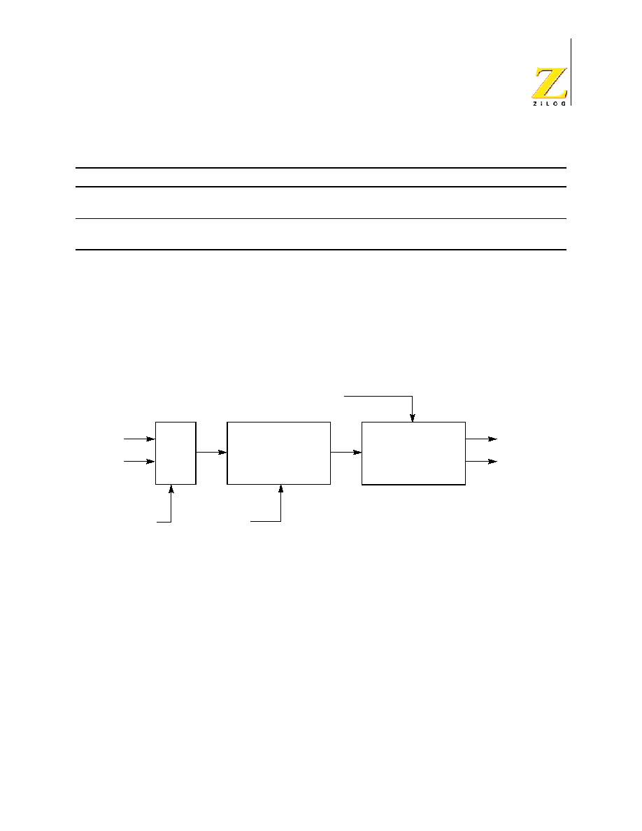
Functional Description
This device incorporates special functions to enhance the Z8
Æ
' functionality in
consumer and battery-operated applications.
Program Memory
This device addresses up to 32KB of OTP memory. The first 12 Bytes are
reserved for interrupt vectors. These locations contain the six 16-bit vectors that
correspond to the six available interrupts.
RAM
This device features 256B of RAM. See Figure 14.
Note:
Note:

Z8 GP
TM
OTP MCU Family
Product Specification
PS023702-1004
P r e l i m i n a r y Functional
Description
24
Figure 14. Program Memory Map (32K OTP)
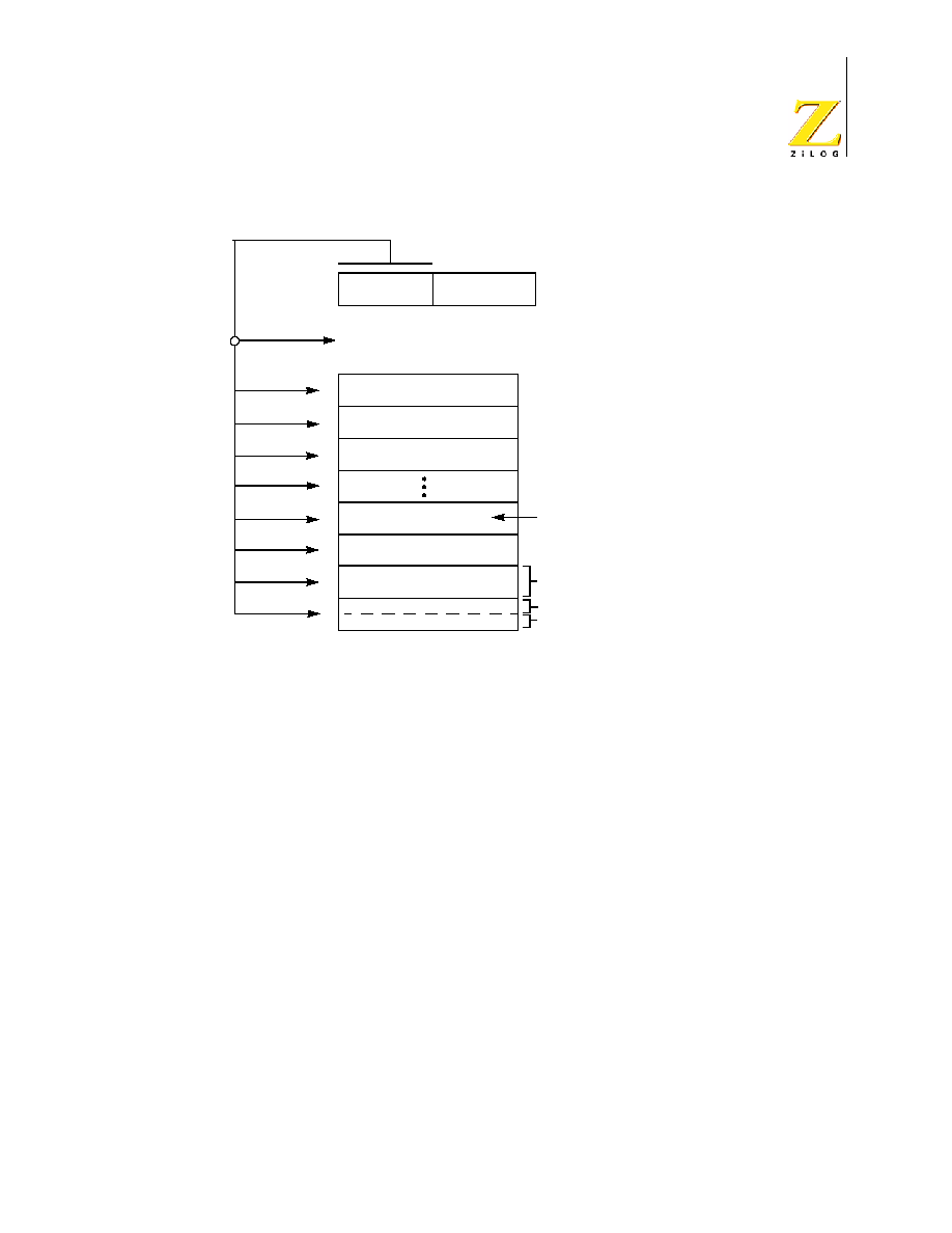
Expanded Register File
The register file has been expanded to allow for additional system control regis-
ters and for mapping of additional peripheral devices into the register address
area. The Z8
Æ
register address space (R0 through R15) has been implemented
as 16 banks, with 16 registers per bank. These register groups are known as the
On-Chip
ROM
Reset Start Address
IRQ5
IRQ5
IRQ4
IRQ4
IRQ3
IRQ3
IRQ2
IRQ2
IRQ1
IRQ1
IRQ0
IRQ0
12
11
10
9
8
7
6
5
4
3
2
1
0
32768
Location of
first Byte of
instruction
executed
after RESET
Interrupt Vector
(Lower Byte)
Interrupt Vector
(Upper Byte)
Not Accessible

Z8 GP
TM
OTP MCU Family
Product Specification
PS023702-1004
P r e l i m i n a r y Functional
Description
25
ERF (Expanded Register File). Bits 7≠4 of register RP select the working register
group. Bits 3≠0 of register RP select the expanded register file bank.
An expanded register bank is also referred to as an expanded
register group (see Figure 15).
Note:

Z8 GP
TM
OTP MCU Family
Product Specification
PS023702-1004
P r e l i m i n a r y Functional
Description
26
Figure 15. Expanded Register File Architecture
U U U U U U U 0
0 0 0 0 0 0 0 0
0 0 0 0 0 0 0 0
0 0 0 0 0 0 0 0
00
0F
7F
F0
FF
FF SPL
0 0 0 0 0 0 0 0
U U U U U U U U
0 0 0 0 0 0 0 0
U U U U U U U U
U U U U U U U U
U U U U U U U U
1 1 1 1 1 1 1 1
0 0 0 0 0 0 0 0
1 1 0 0 1 1 1 1
U U U U U U U U
U U U U U U U U
U U U U U U U U
U U U U U U U U
U U U U U U U U
FE SPH
FD RP
FC FLAGS
FB IMR
FA IRQ
F9 IPR
F8 P01M
F7 P3M
F6 P2M
F5 Reserved
F4 Reserved
F3 Reserved
F2 Reserved
F1 Reserved
F0 Reserved
D7 D6 D5 D4 D3 D2 D1 D0
U U 0 0 1 1 0 1
U 0 1 0 0 0 U 0
1 1 1 1 1 1 1 0
(F) 0F WDTMR
(F) 0E Reserved
(F) 0D SMR2
(F) 0C Reserved
(F) 0B SMR
(F) 0A Reserved
(F) 09 Reserved
(F) 08 Reserved
(F) 07 Reserved
(F) 06 Reserved
(F) 05 Reserved
(F) 04 Reserved
(F) 03 Reserved
(F) 02 Reserved
(F) 01 Reserved
(F) 00 PCON
7 6 5 4 3 2 1 0
Expanded Register
Bank Pointer
Working Register
U U U U U U U U
U U U U U U U U
0 0 0 0 0 0 0 0
(D) 0C LVD
(D) 0B HI8
(D) 0A LO8
(D) 09 HI16
(D) 08 LO16
(D) 07 TC16H
(D) 06 TC16L
(D) 05 TC8H
(D) 04 TC8L
(D) 03 CTR3
(D) 02 CTR2
(D) 01 CTR1
(D) 00 CTR0
Group Pointer
Register File (Bank 0)**
0 0 0 1 1 1 1 1
*
*
0 0 0 0 0 0 0 0
0 0 0 0 0 0 0 0
0 0 0 0 0 0 0 0
0 0 0 0 0 0 0 0
0 0 0 0 0 0 0 0
0 0 0 0 0 0 0 0
0 0 0 0 0 0 0 0
0 0 0 0 0 0 0 0
U = Unknown
* Is not reset with a Stop-Mode Recovery
** All addresses are in hexadecimal
Is not reset with a Stop-Mode Recovery, except Bit 0
Bit 5 Is not reset with a Stop-Mode Recovery
Bits 5,4,3,2 not reset with a Stop-Mode Recovery
Bits 5 and 4 not reset with a Stop-Mode Recovery
Bits 5,4,3,2,1 not reset with a Stop-Mode Recovery
Expanded Reg. Bank 0/Group (0)
*
(0) 03 P3
(0) 02 P2
(0) 01 P1
(0) 00 P0
0
U
U
U
U
*
*
*
*
*
*
*
*
*
*
*
Expanded Reg. Bank F/Group 0**
Expanded Reg. Bank 0/Group 15**
Register Pointer
Z8
Æ
Standard Control Registers
Expanded Reg. Bank D/Group 0
Reset
Condition
Z8 GP
TM
OTP MCU Family
Product Specification
PS023702-1004
P r e l i m i n a r y Functional
Description
27
The upper nibble of the register pointer (see Figure 16) selects which working reg-
ister group, of 16 bytes in the register file, is accessed out of the possible 256. The
lower nibble selects the expanded register file bank and, in the case of the Z8 GP
family, banks 0, F, and D are implemented. A
0H
in the lower nibble allows the nor-
mal register file (bank 0) to be addressed. Any other value from
1H
to
FH
exchanges the lower 16 registers to an expanded register bank.
Figure 16. Register Pointer
Example: Z8 GP: (See Figure 15 on page 26)
R253 RP = 00h
R0 = Port 0
R1 = Port 1
R2 = Port 2
R3 = Port 3
But if:
R253 RP = 0Dh
R0 = CTRL0
R1 = CTRL1
R2 = CTRL2
R3 = Reserved
R253 RP
D7
D6
D5
D4
D3
D2
D1
D0
Expanded Register
File Pointer
Working Register
Pointer
Default Setting After Reset = 0000 0000

Z8 GP
TM
OTP MCU Family
Product Specification
PS023702-1004
P r e l i m i n a r y Functional
Description
28
The counter/timers are mapped into ERF group D. Access is easily performed
using the following:
LD
RP, #0Dh
; Select ERF D
for access to bank D
; (working
register group 0)
LD
R0,#xx
; load CTRL0
LD
1, #xx
; load CTRL1
LD
R1, 2
; CTRL2
CTRL1
LD
RP, #0Dh
; Select ERF D
for access to bank D
; (working
register group 0)
LD
RP, #7Dh
; Select
expanded register bank D and working
; register
group 7 of bank 0 for access.
LD
71h, 2
; CTRL2
register 71h
LD
R1, 2
; CTRL2
register 71h
Register File
The register file (bank 0) consists of 4 I/O port registers, 237 general-purpose reg-
isters, 16 control and status registers (R0≠R3, R4≠R239, and R240≠R255,
respectively), and two expanded registers groups in Banks D (see Table 12) and
F. Instructions can access registers directly or indirectly through an 8-bit address
field, thereby allowing a short, 4-bit register address to use the Register Pointer
(Figure 17). In the 4-bit mode, the register file is divided into 16 working register
groups, each occupying 16 continuous locations. The Register Pointer addresses
the starting location of the active working register group.
Working register group E0≠EF can only be accessed through
working registers and indirect addressing modes.
Note:
Z8 GP
TM
OTP MCU Family
Product Specification
PS023702-1004
P r e l i m i n a r y Functional
Description
29
Figure 17. Register Pointer--Detail
Stack
The internal register file is used for the stack. An 8-bit Stack Pointer SPL (R255) is
used for the internal stack that resides in the general-purpose registers (R4≠
R239). SPH (R254) can be used as a general-purpose register.
R
7
R
6
R
5
R
4
R
3
R
2
R
1
R
The upper nibble of the register file address
provided by the register pointer specifies the
active working-register group.
Specified Working
Register Group
Register Group 1
Register Group 0
I/O Ports
R253
The lower nibble of the
register file address provided
by the instruction points to
the specified register.
* RP = 00: Selects Register Bank 0, Working Register Group 0
R15 to R0
R15 to R4 *
R3 to R0 *
FF
F0
EF
E0
DF
D0
40
3F
30
2F
20
1F
10
0F
00
Register Group 2

Z8 GP
TM
OTP MCU Family
Product Specification
PS023702-1004
P r e l i m i n a r y Functional
Description
30
Timers
T8_Capture_HI--HI8(D)0BH
This register holds the captured data from the output of the 8-bit Counter/Timer0.
Typically, this register holds the number of counts when the input signal is 1.
T8_Capture_LO--L08(D)0AH
This register holds the captured data from the output of the 8-bit Counter/Timer0.
Typically, this register holds the number of counts when the input signal is 0.
T16_Capture_HI--HI16(D)09H
This register holds the captured data from the output of the 16-bit Counter/
Timer16. This register holds the MS-Byte of the data.
T16_Capture_LO--L016(D)08H
This register holds the captured data from the output of the 16-bit Counter/
Timer16. This register holds the LS-Byte of the data.
Counter/Timer2 MS-Byte Hold Register--TC16H(D)07H
Field
Bit Position
Description
T8_Capture_HI
[7:0]
R/W
Captured Data - No Effect
Field
Bit Position
Description
T8_Capture_L0
[7:0]
R/W Captured Data - No Effect
Field
Bit Position
Description
T16_Capture_HI [7:0]
R/W Captured Data - No Effect
Field
Bit Position
Description
T16_Capture_LO [7:0]
R/W Captured Data - No Effect
Field
Bit Position
Description
T16_Data_HI
[7:0]
R/W Data

Z8 GP
TM
OTP MCU Family
Product Specification
PS023702-1004
P r e l i m i n a r y Functional
Description
31
Counter/Timer2 LS-Byte Hold Register--TC16L(D)06H
Counter/Timer8 High Hold Register--TC8H(D)05H
Counter/Timer8 Low Hold Register--TC8L(D)04H
CTR0 Counter/Timer8 Control Register--CTR0(D)00H
Table 12 lists and briefly describes the fields for this register.
Field
Bit Position
Description
T16_Data_LO
[7:0]
R/W Data
Field
Bit Position
Description
T8_Level_HI
[7:0]
R/W Data
Field
Bit Position
Description
T8_Level_LO
[7:0]
R/W Data
Table 12. CTR0(D)00H Counter/Timer8 Control Register
Field
Bit Position
Value
Description
T8_Enable
7-------
R/W
0*
1
0
1
Counter Disabled
Counter Enabled
Stop Counter
Enable Counter
Single/Modulo-N
-6-------
R/W
0
1
Modulo-N
Single Pass
Time_Out
--5------
R/W
0
1
0
1
No Counter Time-Out
Counter Time-Out Occurred
No Effect
Reset Flag to 0
T8 _Clock
---43---
R/W
0 0
0 1
1 0
1 1
SCLK
SCLK/2
SCLK/4
SCLK/8
Capture_INT_Mask
-----2--
R/W
0
1
Disable Data Capture Interrupt
Enable Data Capture Interrupt

Z8 GP
TM
OTP MCU Family
Product Specification
PS023702-1004
P r e l i m i n a r y Functional
Description
32
T8 Enable
This field enables T8 when set (written) to 1.
Single/Modulo-N
When set to 0 (Modulo-N), the counter reloads the initial value when the terminal
count is reached. When set to 1 (single-pass), the counter stops when the termi-
nal count is reached.
Timeout
This bit is set when T8 times out (terminal count reached). To reset this bit, write a
1 to its location.
Writing a 1 is the only way to reset the Terminal Count
status condition. Reset this bit before using/enabling the
counter/timers.
The first clock of T8 might not have complete clock width
and can occur any time when enabled.
Take care when using the OR or AND commands to manipulate
CTR0, bit 5 and CTR1, bits 0 and 1 (Demodulation Mode).
These instructions use a Read-Modify-Write sequence in which
the current status from the CTR0 and CTR1 registers is ORed
or ANDed with the designated value and then written back into
the registers.
T8 Clock
This bit defines the frequency of the input signal to T8.
Counter_INT_Mask
------1-
R/W
0
1
Disable Time-Out Interrupt
Enable Time-Out Interrupt
P34_Out
-------0
R/W
0*
1
P34 as Port Output
T8 Output on P34
Note:
*
Indicates the value upon Power-On Reset.
Table 12. CTR0(D)00H Counter/Timer8 Control Register (Continued)
Field
Bit Position
Value
Description
Caution:
Note:

Z8 GP
TM
OTP MCU Family
Product Specification
PS023702-1004
P r e l i m i n a r y Functional
Description
33
Capture_INT_Mask
Set this bit to allow an interrupt when data is captured into either LO8 or HI8 upon
a positive or negative edge detection in demodulation mode.
Counter_INT_Mask
Set this bit to allow an interrupt when T8 has a timeout.
P34_Out
This bit defines whether P34 is used as a normal output pin or the T8 output.
T8 and T16 Common Functions--CTR1(0D)01H
This register controls the functions in common with the T8 and T16.
Table 13 lists and briefly describes the fields for this register.
Table 13. CTR1(0D)01H T8 and T16 Common Functions
Field
Bit Position
Value
Description
Mode
7-------
R/W
0*
Transmit Mode
Demodulation Mode
P36_Out/
Demodulator_Input
-6------
R/W
0*
1
0
1
Transmit Mode
Port Output
T8/T16 Output
Demodulation Mode
P31
P20
T8/T16_Logic/
Edge _Detect
--54----
R/W
00**
01
10
11
00**
01
10
11
Transmit Mode
AND
OR
NOR
NAND
Demodulation Mode
Falling Edge
Rising Edge
Both Edges
Reserved

Z8 GP
TM
OTP MCU Family
Product Specification
PS023702-1004
P r e l i m i n a r y Functional
Description
34
Mode
If the result is 0, the counter/timers are in TRANSMIT mode; otherwise, they are in
DEMODULATION mode.
P36_Out/Demodulator_Input
In TRANSMIT Mode, this bit defines whether P36 is used as a normal output pin
or the combined output of T8 and T16.
In DEMODULATION Mode, this bit defines whether the input signal to the
Counter/Timers is from P20 or P31.
If the input signal is from Port 31, a capture event may also generate an IRQ2
interrupt. To prevent generating an IRQ2, either disable the IRQ2 interrupt by
clearing its IMR bit D2 or use P20 as the input.
Transmit_Submode/
Glitch_Filter
----32--
R/W
00*
01
10
11
00*
01
10
11
Transmit Mode
Normal Operation
Ping-Pong Mode
T16_Out = 0
T16_Out = 1
Demodulation Mode
No Filter
4 SCLK Cycle
8 SCLK Cycle
Reserved
Initial_T8_Out/
Rising Edge
------1-
R/W
R
W
0*
1
0*
1
0
1
Transmit Mode
T8_OUT is 0 Initially
T8_OUT is 1 Initially
Demodulation Mode
No Rising Edge
Rising Edge Detected
No Effect
Reset Flag to 0
Initial_T16_Out/
Falling_Edge
-------0
R/W
R
W
0*
1
0*
1
0
1
Transmit Mode
T16_OUT is 0 Initially
T16_OUT is 1 Initially
Demodulation Mode
No Falling Edge
Falling Edge Detected
No Effect
Reset Flag to 0
Note:
*Default at Power-On Reset.
**Default at Power-On Reset.Not reset with Stop Mode recovery.
Table 13. CTR1(0D)01H T8 and T16 Common Functions (Continued)
Field
Bit Position
Value
Description

Z8 GP
TM
OTP MCU Family
Product Specification
PS023702-1004
P r e l i m i n a r y Functional
Description
35
T8/T16_Logic/Edge _Detect
In TRANSMIT Mode, this field defines how the outputs of T8 and T16 are com-
bined (AND, OR, NOR, NAND).
In DEMODULATION Mode, this field defines which edge should be detected by
the edge detector.
Transmit_Submode/Glitch Filter
In Transmit Mode, this field defines whether T8 and T16 are in the PING-PONG
mode or in independent normal operation mode. Setting this field to "NORMAL
OPERATION Mode" terminates the "PING-PONG Mode" operation. When set to
10, T16 is immediately forced to a 0; a setting of 11 forces T16 to output a 1.
In DEMODULATION Mode, this field defines the width of the glitch that must be fil-
tered out.
Initial_T8_Out/Rising_Edge
In TRANSMIT Mode, if 0, the output of T8 is set to 0 when it starts to count. If 1,
the output of T8 is set to 1 when it starts to count. When the counter is not enabled
and this bit is set to 1 or 0, T8_OUT is set to the opposite state of this bit. This
ensures that when the clock is enabled, a transition occurs to the initial state set
by CTR1, D1.
In DEMODULATION Mode, this bit is set to 1 when a rising edge is detected in the
input signal. In order to reset the mode, a 1 should be written to this location.
Initial_T16 Out/Falling _Edge
In TRANSMIT Mode, if it is 0, the output of T16 is set to 0 when it starts to count. If
it is 1, the output of T16 is set to 1 when it starts to count. This bit is effective only
in Normal or PING-PONG Mode (CTR1, D3; D2). When the counter is not enabled
and this bit is set, T16_OUT is set to the opposite state of this bit. This ensures
that when the clock is enabled, a transition occurs to the initial state set by CTR1,
D0.
In DEMODULATION Mode, this bit is set to 1 when a falling edge is detected in
the input signal. In order to reset it, a 1 should be written to this location.
Modifying CTR1 (D1 or D0) while the counters are enabled
causes unpredictable output from T8/16_OUT.
CTR2 Counter/Timer 16 Control Register--CTR2(D)02H
Table 14 lists and briefly describes the fields for this register.
Note:

Z8 GP
TM
OTP MCU Family
Product Specification
PS023702-1004
P r e l i m i n a r y Functional
Description
36
T16_Enable
This field enables T16 when set to 1.
Single/Modulo-N
In TRANSMIT Mode, when set to 0, the counter reloads the initial value when it
reaches the terminal count. When set to 1, the counter stops when the terminal
count is reached.
Table 14. CTR2(D)02H: Counter/Timer16 Control Register
Field
Bit Position
Value
Description
T16_Enable
7-------
R
W
0*
1
0
1
Counter Disabled
Counter Enabled
Stop Counter
Enable Counter
Single/Modulo-N
-6------
R/W
0*
1
0
1
Transmit Mode
Modulo-N
Single Pass
Demodulation Mode
T16 Recognizes Edge
T16 Does Not Recognize
Edge
Time_Out
--5-----
R
W
0*
1
0
1
No Counter Timeout
Counter Timeout
Occurred
No Effect
Reset Flag to 0
T16 _Clock
---43---
R/W
00**
01
10
11
SCLK
SCLK/2
SCLK/4
SCLK/8
Capture_INT_Mask
-----2--
R/W
0**
1
Disable Data Capture Int.
Enable Data Capture Int.
Counter_INT_Mask
------1-
R/W
0
1
Disable Timeout Int.
Enable Timeout Int.
P35_Out
-------0
R/W
0*
1
P35 as Port Output
T16 Output on P35
Note:
*Indicates the value upon Power-On Reset.
**Indicates the value upon Power-On Reset.Not reset with Stop Mode recovery.

Z8 GP
TM
OTP MCU Family
Product Specification
PS023702-1004
P r e l i m i n a r y Functional
Description
37
In Demodulation Mode, when set to 0, T16 captures and reloads on detection of
all the edges. When set to 1, T16 captures and detects on the first edge but
ignores the subsequent edges. For details, see the description of T16 Demodula-
tion Mode on page 45.
Time_Out
This bit is set when T16 times out (terminal count reached). To reset the bit, write
a 1 to this location.
T16_Clock
This bit defines the frequency of the input signal to Counter/Timer16.
Capture_INT_Mask
This bit is set to allow an interrupt when data is captured into LO16 and HI16.
Counter_INT_Mask
Set this bit to allow an interrupt when T16 times out.
P35_Out
This bit defines whether P35 is used as a normal output pin or T16 output.
CTR3 T8/T16 Control Register--CTR3(D)03H
Table 15 lists and briefly describes the fields for this register. This register allows
the T
8
and T
16
counters to be synchronized.
Table 15. CTR3 (D)03H: T8/T16 Control Register
Field
Bit Position
Value
Description
T
16
Enable
7-------
R
R
W
W
0*
1
0
1
Counter Disabled
Counter Enabled
Stop Counter
Enable Counter
T
8
Enable
-6------
R
R
W
W
0*
1
0
1
Counter Disabled
Counter Enabled
Stop Counter
Enable Counter
Sync Mode
--5-----
R/W
0**
1
Disable Sync Mode
Enable Sync Mode
Z8 GP
TM
OTP MCU Family
Product Specification
PS023702-1004
P r e l i m i n a r y Functional
Description
38
Counter/Timer Functional Blocks
Input Circuit
The edge detector monitors the input signal on P31 or P20. Based on CTR1 D5≠
D4, a pulse is generated at the Pos Edge or Neg Edge line when an edge is
detected. Glitches in the input signal that have a width less than specified (CTR1
D3, D2) are filtered out (see Figure 18).
Figure 18. Glitch Filter Circuitry
T8 Transmit Mode
Before T8 is enabled, the output of T8 depends on CTR1, D1. If it is 0, T8_OUT is
1; if it is 1, T8_OUT is 0. See Figure 19.
Reserved
---43210
R
W
1
x
Always reads
11111
No Effect
Note:
*Indicates the value upon Power-On Reset.
**Indicates the value upon Power-On Reset. Not reset with Stop Mode recovery.
Table 15. CTR3 (D)03H: T8/T16 Control Register (Continued)
Field
Bit Position
Value
Description
MUX
Glitch
Filter
Edge
Detector
P31
P20
Pos
Edge
Neg
Edge
CTR1
D5,D4
CTR1
D6
CTR1
D3, D2

Z8 GP
TM
OTP MCU Family
Product Specification
PS023702-1004
P r e l i m i n a r y Functional
Description
39
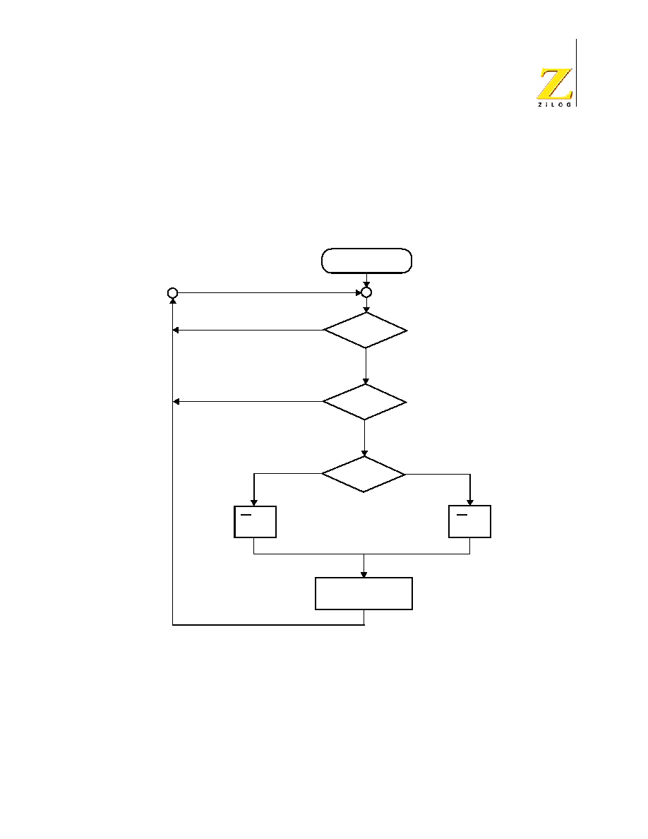
Figure 19. Transmit Mode Flowchart
Set Timeout Status Bit
(CTR0 D5) and Generate
Timeout_Int if Enabled
Set Timeout Status Bit
(CTR0 D5) and Generate
Timeout_Int if Enabled
T8 (8-Bit)
Transmit Mode
No
T8_Enable Bit Set
CTR0, D7
Yes
CTR1, D1
Value
Reset T8_Enable Bit
0
1
Load TC8L
Reset T8_OUT
Load TC8H
Set T8_OUT
Enable T8
No
T8_Timeout
Yes
Single Pass
Single
Modulo-N
T8_OUT Value
0
Enable T8
No
T8_Timeout
Yes
Pass?
Load TC8H
Set T8_OUT
Load TC8L
Reset T8_OUT
1
Z8 GP
TM
OTP MCU Family
Product Specification
PS023702-1004
P r e l i m i n a r y Functional
Description
40
When T8 is enabled, the output T8_OUT switches to the initial value (CTR1, D1).
If the initial value (CTR1, D1) is 0, TC8L is loaded; otherwise, TC8H is loaded into
the counter. In SINGLE-PASS Mode (CTR0, D6), T8 counts down to 0 and stops,
T8_OUT toggles, the timeout status bit (CTR0, D5) is set, and a timeout interrupt
can be generated if it is enabled (CTR0, D1). In Modulo-N Mode, upon reaching
terminal count, T8_OUT is toggled, but no interrupt is generated. From that point,
T8 loads a new count (if the T8_OUT level now is 0), TC8L is loaded; if it is 1,
TC8H is loaded. T8 counts down to 0, toggles T8_OUT, and sets the timeout sta-
tus bit (CTR0, D5), thereby generating an interrupt if enabled (CTR0, D1). One
cycle is thus completed. T8 then loads from TC8H or TC8L according to the
T8_OUT level and repeats the cycle. See Figure 20.
Figure 20. 8-Bit Counter/Timer Circuits
You can modify the values in TC8H or TC8L at any time. The new values take
effect when they are loaded.
To ensure known operation do not write these registers at
the time the values are to be loaded into the counter/timer.
An initial count of 1 is not allowed (a non-function occurs).
An
initial count of 0 causes TC8 to count from 0 to
FFH
to
FEH
.
CTR0 D1
Negative Edge
Positive Edge
Z8
Æ
Data Bus
IRQ4
CTR0 D2
SCLK
Z8
Æ
Data Bus
CTR0 D4, D3
Clock
T8_OUT
LO8
TC8H
TC8L
Clock
Select
8-Bit
Counter T8
HI8
Caution:
Z8 GP
TM
OTP MCU Family
Product Specification
PS023702-1004
P r e l i m i n a r y Functional
Description
41
The letter
h
denotes hexadecimal values.
Transition from 0 to
FFh
is not a timeout condition.
Using the same instructions for stopping the counter/timers
and setting the status bits is not recommended.
Two successive commands are necessary. First, the counter/timers must be
stopped. Second, the status bits must be reset. These commands are required
because it takes one counter/timer clock interval for the initiated event to actually
occur. See Figure 21 and Figure 22.
Figure 21. T8_OUT in Single-Pass Mode
Figure 22. T8_OUT in Modulo-N Mode
T8 Demodulation Mode
The user must program TC8L and TC8H to
FFH
. After T8 is enabled, when the first
edge (rising, falling, or both depending on CTR1, D5; D4) is detected, it starts to
count down. When a subsequent edge (rising, falling, or both depending on
CTR1, D5; D4) is detected during counting, the current value of T8 is comple-
mented and put into one of the capture registers. If it is a positive edge, data is put
Note:
Caution:
TC8H
Counts
Counter Enable Command;
T8_OUT Switches to Its
Initial Value (CTR1 D1)
T8_OUT Toggles;
Timeout Interrupt
Counter Enable Command;
T8_OUT Switches to Its
Initial Value (CTR1 D1)
Timeout
Interrupt
Timeout
Interrupt
T8_OUT
T8_OUT Toggles
TC8L
TC8H
TC8H
TC8L
TC8L
. . .
Z8 GP
TM
OTP MCU Family
Product Specification
PS023702-1004
P r e l i m i n a r y Functional
Description
42
into LO8; if it is a negative edge, data is put into HI8. From that point, one of the
edge detect status bits (CTR1, D1; D0) is set, and an interrupt can be generated if
enabled (CTR0, D2). Meanwhile, T8 is loaded with
FFh
and starts counting again.
If T8 reaches 0, the timeout status bit (CTR0, D5) is set, and an interrupt can be
generated if enabled (CTR0, D1). T8 then continues counting from
FFH
(see
Figure 23 and Figure 24).
Figure 23. Demodulation Mode Count Capture Flowchart
T8 (8-Bit)
Count Capture
T8 Enable
(Set by User)
No
Yes
Edge Present
What Kind
of Edge
T8 HI8
No
Yes
Negative
FFh
T8
Positive
T8 LO8
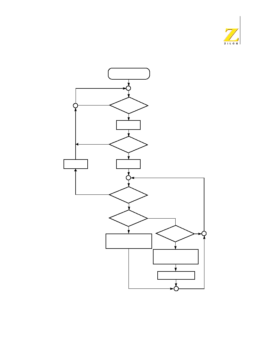
Z8 GP
TM
OTP MCU Family
Product Specification
PS023702-1004
P r e l i m i n a r y Functional
Description
43
Figure 24. Demodulation Mode Flowchart
T8 (8-Bit)
Demodulation Mode
T8 Enable
CTR0, D7
No
Yes
FFH
TC8
First
Edge Present
Enable TC8
T8_Enable
Bit Set
Edge Present
T8 Timeout
Set Edge Present Status
Bit and Trigger Data
Capture Int. If Enabled
Set Timeout Status
Bit and Trigger
Timeout Int. If Enabled
Continue Counting
Disable TC8
No
Yes
No
Yes
Yes
Yes
No
No

Z8 GP
TM
OTP MCU Family
Product Specification
PS023702-1004
P r e l i m i n a r y Functional
Description
44
T16 Transmit Mode
In NORMAL or PING-PONG mode, the output of T16 when not enabled, is depen-
dent on CTR1, D0. If it is a 0, T16_OUT is a 1; if it is a 1, T16_OUT is 0. You can
force the output of T16 to either a 0 or 1 whether it is enabled or not by program-
ming CTR1 D3; D2 to a 10 or 11.
When T16 is enabled, TC16H * 256 + TC16L is loaded, and T16_OUT is switched
to its initial value (CTR1, D0). When T16 counts down to 0, T16_OUT is toggled
(in NORMAL or PING-PONG mode), an interrupt (CTR2, D1) is generated (if
enabled), and a status bit (CTR2, D5) is set. See Figure 25.
Figure 25. 16-Bit Counter/Timer Circuits
Global interrupts override this function as described in
"Interrupts" on page 48.
If T16 is in SINGLE-PASS mode, it is stopped at this point (see Figure 26). If it is
in Modulo-N Mode, it is loaded with TC16H * 256 + TC16L, and the counting con-
tinues (see Figure 27).
You can modify the values in TC16H and TC16L at any time. The new values take
effect when they are loaded.
CTR2 D1
Negative Edge
Positive Edge
Z8
Æ
Data Bus
IRQ3
CTR2 D2
SCLK
Z8
Æ
Data Bus
CTR2 D4, D3
Clock
T16_OUT
LO16
TC16H
TC16L
Clock
Select
16-Bit
Counter T16
HI16
Note:

Z8 GP
TM
OTP MCU Family
Product Specification
PS023702-1004
P r e l i m i n a r y Functional
Description
45
Do not load these registers at the time the values are to be
loaded into the counter/timer to ensure known operation.
An initial count of 1 is not allowed. An initial count of 0
causes T16 to count from 0 to
FFFFH
to
FFFEH
. Transition
from 0 to
FFFFH
is not a timeout condition.
Figure 26. T16_OUT in Single-Pass Mode
Figure 27. T16_OUT in Modulo-N Mode
T16 DEMODULATION Mode
The user must program TC16L and TC16H to
FFH
. After T16 is enabled, and the
first edge (rising, falling, or both depending on CTR1 D5; D4) is detected, T16
captures HI16 and LO16, reloads, and begins counting.
If D6 of CTR2 Is 0
When a subsequent edge (rising, falling, or both depending on CTR1, D5; D4) is
detected during counting, the current count in T16 is complemented and put into
HI16 and LO16. When data is captured, one of the edge detect status bits (CTR1,
D1; D0) is set, and an interrupt is generated if enabled (CTR2, D2). T16 is loaded
with
FFFFH
and starts again.
This T16 mode is generally used to measure space time, the length of time
between bursts of carrier signal (marks).
Caution:
TC16H*256+TC16L Counts
"Counter Enable" Command
T16_OUT Switches to Its
Initial Value (CTR1 D0)
T16_OUT Toggles,
Timeout Interrupt
TC16H*256+TC16L
TC16H*256+TC16L
TC16H*256+TC16L
T16_OUT Toggles,
Timeout Interrupt
T16_OUT Toggles,
Timeout Interrupt
"Counter Enable" Command,
T16_OUT Switches to Its
Initial Value (CTR1 D0)
TC16_OUT
. . .

Z8 GP
TM
OTP MCU Family
Product Specification
PS023702-1004
P r e l i m i n a r y Functional
Description
46
If D6 of CTR2 Is 1
T16 ignores the subsequent edges in the input signal and continues counting
down. A timeout of T8 causes T16 to capture its current value and generate an
interrupt if enabled (CTR2, D2). In this case, T16 does not reload and continues
counting. If the D6 bit of CTR2 is toggled (by writing a 0 then a 1 to it), T16 cap-
tures and reloads on the next edge (rising, falling, or both depending on CTR1,
D5; D4), continuing to ignore subsequent edges.
This T16 mode generally measures mark time, the length of an active carrier sig-
nal burst.
If T16 reaches 0, T16 continues counting from
FFFFh
. Meanwhile, a status bit
(CTR2 D5) is set, and an interrupt timeout can be generated if enabled (CTR2
D1).
Ping-Pong Mode
This operation mode is only valid in TRANSMIT Mode. T8 and T16 must be pro-
grammed in Single-Pass mode (CTR0, D6; CTR2, D6), and Ping-Pong mode
must be programmed in CTR1, D3; D2. The user can begin the operation by
enabling either T8 or T16 (CTR0, D7 or CTR2, D7). For example, if T8 is enabled,
T8_OUT is set to this initial value (CTR1, D1). According to T8_OUT's level,
TC8H or TC8L is loaded into T8. After the terminal count is reached, T8 is dis-
abled, and T16 is enabled. T16_OUT then switches to its initial value (CTR1, D0),
data from TC16H and TC16L is loaded, and T16 starts to count. After T16 reaches
the terminal count, it stops, T8 is enabled again, repeating the entire cycle. Inter-
rupts can be allowed when T8 or T16 reaches terminal control (CTR0, D1; CTR2,
D1). To stop the ping-pong operation, write 00 to bits D3 and D2 of CTR1. See
Figure 28.
Enabling ping-pong operation while the counter/timers are
running might cause intermittent counter/timer function. Disable
the counter/timers and reset the status flags before instituting
this operation.
Note:
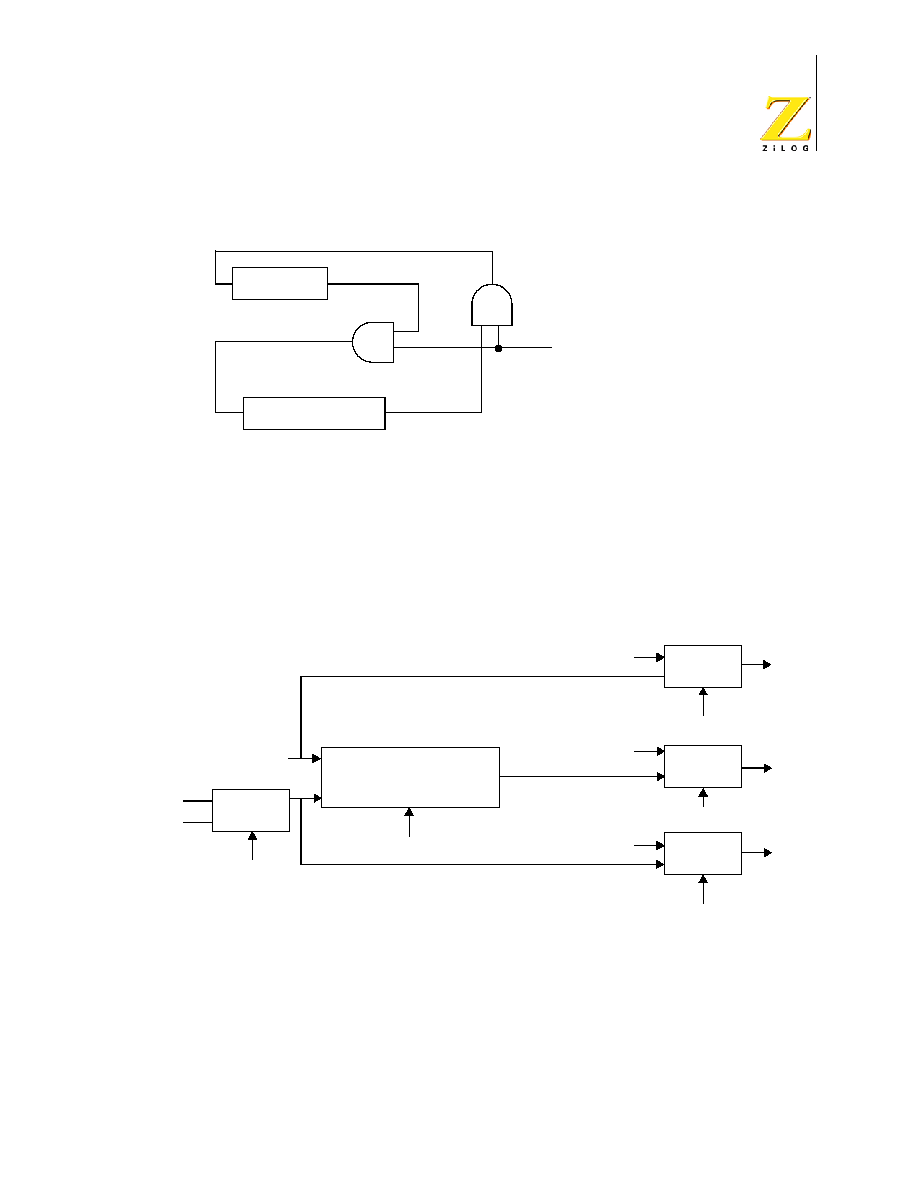
Z8 GP
TM
OTP MCU Family
Product Specification
PS023702-1004
P r e l i m i n a r y Functional
Description
47
Figure 28. Ping-Pong Mode Diagram
Initiating PING-PONG Mode
First, make sure both counter/timers are not running. Set T8 into Single-Pass
mode (CTR0, D6), set T16 into SINGLE-PASS mode (CTR2, D6), and set the
Ping-Pong mode (CTR1, D2; D3). These instructions can be in random order.
Finally, start PING-PONG mode by enabling either T8 (CTR0, D7) or T16 (CTR2,
D7). See Figure 29.
Figure 29. Output Circuit
The initial value of T8 or T16 must not be
1
. Stopping the timer and restarting the
timer reloads the initial value to avoid an unknown previous value.
Enable
TC8
Enable
Timeout
TC16
Ping-Pong
CTR1 D3,D2
Timeout
T16_OUT
MUX
CTR1 D3
T8_OUT
P34
AND/OR/NOR/NAND
Logic
MUX
MUX
MUX
P35
P36
P34_Internal
CTR1 D5, D4
P36_Internal
P35_Internal
CTR1, D2
CTR0 D0
CTR1 D6
CTR2 D0

Z8 GP
TM
OTP MCU Family
Product Specification
PS023702-1004
P r e l i m i n a r y Functional
Description
48
During PING-PONG Mode
The enable bits of T8 and T16 (CTR0, D7; CTR2, D7) are set and cleared alter-
nately by hardware. The timeout bits (CTR0, D5; CTR2, D5) are set every time the
counter/timers reach the terminal count.
Timer Output
The output logic for the timers is illustrated in Figure 29. P34 is used to output T8-
OUT when D0 of CTR0 is set. P35 is used to output the value of TI6-OUT when
D0 of CTR2 is set. When D6 of CTR1 is set, P36 outputs the logic combination of
T8-OUT and T16-OUT determined by D5 and D4 of CTR1.
Interrupts
The Z8 GP
TM
OTP MCU Family features six different interrupts (Table 16). The
interrupts are maskable and prioritized (Figure 30). The six sources are divided as
follows: three sources are claimed by Port 3 lines P33≠P31, two by the counter/
timers (Table 16) and one for low voltage detection. The Interrupt Mask Register
(globally or individually) enables or disables the six interrupt requests.
The source for IRQ is determined by bit 1 of the Port 3 mode register (P3M).
When in digital mode, Pin P33 is the source. When in analog mode the output of
the Stop mode recovery source logic is used as the source for the interrupt. See
Figure 35, Stop Mode Recovery Source, on page 57.
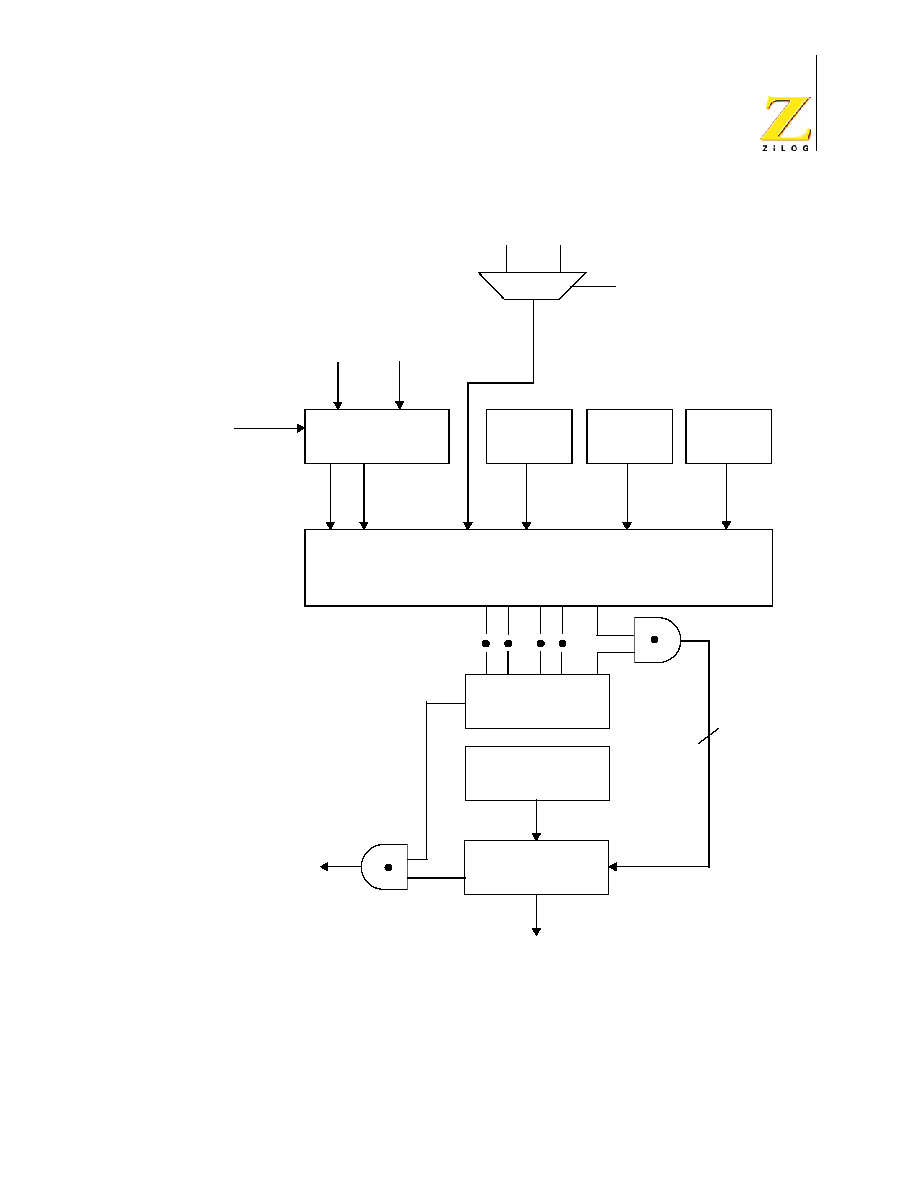
Z8 GP
TM
OTP MCU Family
Product Specification
PS023702-1004
P r e l i m i n a r y Functional
Description
49
Figure 30. Interrupt Block Diagram
Low-Voltage
Detection
Timer 8
Timer 16
Interrupt Edge
Select
IMR
IPR
Priority
Logic
IRQ
5
IRQ2
IRQ0
IRQ1
IRQ3
IRQ4
IRQ5
P31
P32
IRQ Register
D6, D7
Global
Interrupt
Enable
Interrupt
Request
Vector Select
D1 of P3M Register
P33
0
1
Stop Mode Recovery Source

Z8 GP
TM
OTP MCU Family
Product Specification
PS023702-1004
P r e l i m i n a r y Functional
Description
50
When more than one interrupt is pending, priorities are resolved by a programma-
ble priority encoder controlled by the Interrupt Priority Register. An interrupt
machine cycle activates when an interrupt request is granted. As a result, all sub-
sequent interrupts are disabled, and the Program Counter and Status Flags are
saved. The cycle then branches to the program memory vector location reserved
for that interrupt. All Z8 GP
TM
OTP MCU Family interrupts are vectored through
locations in the program memory. This memory location and the next byte contain
the 16-bit address of the interrupt service routine for that particular interrupt
request. To accommodate polled interrupt systems, interrupt inputs are masked,
and the Interrupt Request register is polled to determine which of the interrupt
requests require service.
An interrupt resulting from AN1 is mapped into IRQ2, and an interrupt from AN2 is
mapped into IRQ0. Interrupts IRQ2 and IRQ0 can be rising, falling, or both edge
triggered. These interrupts are programmable by the user. The software can poll
to identify the state of the pin.
Programming bits for the Interrupt Edge Select are located in the IRQ Register
(R250), bits D7 and D6. The configuration is indicated in Table 17.
Table 16. Interrupt Types, Sources, and Vectors
Name
Source
Vector Location
Comments
IRQ0
P32
0,1
External (P32), Rising, Falling Edge Triggered
IRQ1
P33
2,3
External (P33), Falling Edge Triggered
IRQ2
P31, T
IN
4,5
External (P31), Rising, Falling Edge Triggered
IRQ3
T16
6,7
Internal
IRQ4
T8
8,9
Internal
IRQ5
LVD
10,11
Internal
Table 17. IRQ Register
IRQ
Interrupt Edge
D7
D6
IRQ2 (P31)
IRQ0 (P32)
0
0
F
F
0
1
F
R
1
0
R
F
1
1
R/F
R/F
Note: F = Falling Edge; R = Rising Edge
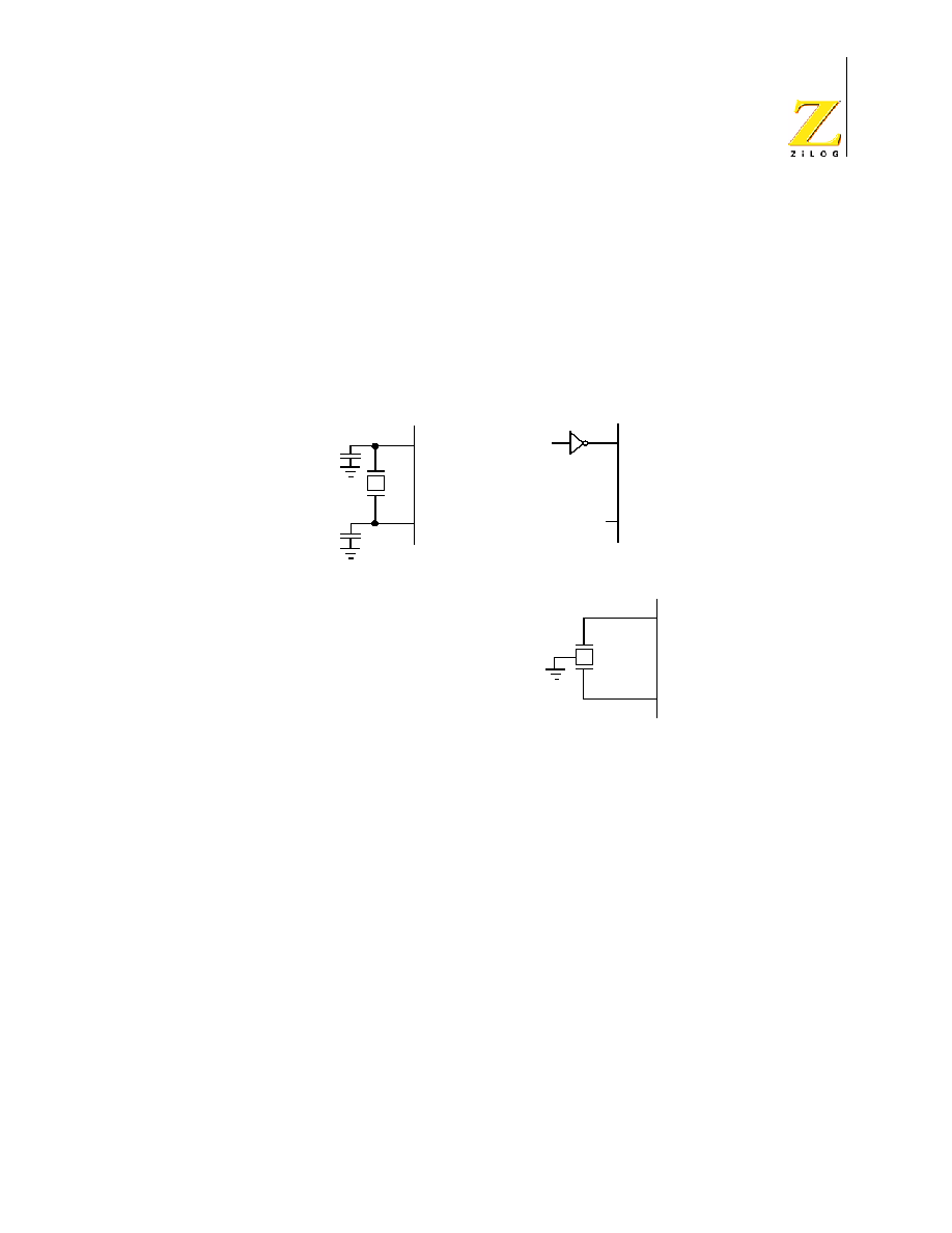
Z8 GP
TM
OTP MCU Family
Product Specification
PS023702-1004
P r e l i m i n a r y Functional
Description
51
Clock
The device's on-chip oscillator has a high-gain, parallel-resonant amplifier, for
connection to a crystal, ceramic resonator, or any suitable external clock source
(XTAL1 = Input, XTAL2 = Output). The crystal must be AT cut, 1 MHz to 8 MHz
maximum, with a series resistance (RS) less than or equal to 100
. The on-chip
oscillator can be driven with a suitable external clock source.
The crystal must be connected across XTAL1 and XTAL2 using the recommended
capacitors (capacitance greater than or equal to 22 pF) from each pin to ground.
Figure 31. Oscillator Configuration
C1
C2
XTAL1
XTAL2
XTAL1
XTAL2
Crystal
C1, C2 = 33pF TYP *
f = 8 MHz
* Preliminary value including pin parasitics
External Clock
XTAL1
XTAL2
Ceramic Resonator f = 8MHz

Z8 GP
TM
OTP MCU Family
Product Specification
PS023702-1004
P r e l i m i n a r y Functional
Description
52
Power-On Reset
A timer circuit clocked by a dedicated on-board RC-oscillator is used for the
Power-On Reset (POR) timer function. The POR time allows V
DD
and the oscilla-
tor circuit to stabilize before instruction execution begins.
The POR timer circuit is a one-shot timer triggered by one of three conditions:
∑
Power Fail to Power OK status, including Waking up from V
BO
Standby
∑
Stop-Mode Recovery (if D5 of SMR = 1)
∑
WDT Timeout
The POR timer is 2.5 ms minimum. Bit 5 of the Stop-Mode Register determines
whether the POR timer is bypassed after Stop-Mode Recovery (typical for external
clock).
HALT Mode
This instruction turns off the internal CPU clock, but not the XTAL oscillation. The
counter/timers and external interrupts IRQ0, IRQ1, IRQ2, IRQ3, IRQ4, and IRQ5
remain active. The devices are recovered by interrupts, either externally or inter-
nally generated. An interrupt request must be executed (enabled) to exit HALT
Mode. After the interrupt service routine, the program continues from the instruc-
tion after HALT Mode.
STOP Mode
This instruction turns off the internal clock and external crystal oscillation, reduc-
ing the standby current to 10
µ
A or less. STOP Mode is terminated only by a
reset, such as WDT timeout, POR, SMR or external reset. This condition causes
the processor to restart the application program at address
000CH
. To enter STOP
(or HALT) mode, first flush the instruction pipeline to avoid suspending execution
in mid-instruction. Execute a NOP (Opcode =
FFH
) immediately before the appro-
priate sleep instruction, as follows:

Z8 GP
TM
OTP MCU Family
Product Specification
PS023702-1004
P r e l i m i n a r y Functional
Description
53
FF
NOP
; clear the pipeline
6F
Stop
; enter Stop Mode
or
FF
NOP
; clear the pipeline
7F
HALT
; enter HALT Mode
Port Configuration Register
The Port Configuration (PCON) register (Figure 32) configures the comparator
output on Port 3. It is located in the expanded register 2 at Bank F, location 00.
PCON(FH)00H
Figure 32. Port Configuration Register (PCON) (Write Only)
Comparator Output Port 3 (D0)
Bit 0 controls the comparator used in Port 3. A 1 in this location brings the compar-
ator outputs to P34 and P37, and a 0 releases the Port to its standard I/O configu-
ration.
Port 1 Output Mode (D1)
Bit 1 controls the output mode of port 1. A 1 in this location sets the output to
push-pull, and a 0 sets the output to open-drain.
D7
D6
D5
D4
D3
D2
D1
D0
Comparator Output Port 3
0 P34, P37 Standard Output*
1 P34, P37 Comparator Output
Port 1
0: Open-Drain
1: Push-Pull*
Port 0
0: Open-Drain
1: Push-Pull*
Reserved (Must be 1)
* Default setting after reset

Z8 GP
TM
OTP MCU Family
Product Specification
PS023702-1004
P r e l i m i n a r y Functional
Description
54
Port 0 Output Mode (D2)
Bit 2 controls the output mode of port 0. A 1 in this location sets the output to
push-pull, and a 0 sets the output to open-drain.
Stop-Mode Recovery Register (SMR)
This register selects the clock divide value and determines the mode of Stop
Mode Recovery (Figure 33). All bits are write only except bit 7, which is read only.
Bit 7 is a flag bit that is hardware set on the condition of Stop recovery and reset
by a power-on cycle. Bit 6 controls whether a low level or a high level at the XOR-
gate input (Figure 35 on page 57) is required from the recovery source. Bit 5 con-
trols the reset delay after recovery. Bits D2, D3, and D4 of the SMR register spec-
ify the source of the Stop Mode Recovery signal. Bits D0 determines if SCLK/
TCLK are divided by 16 or not. The SMR is located in Bank F of the Expanded
Register Group at address
0BH
.

Z8 GP
TM
OTP MCU Family
Product Specification
PS023702-1004
P r e l i m i n a r y Functional
Description
55
SMR(0F)0BH
Figure 33. STOP Mode Recovery Register
SCLK/TCLK Divide-by-16 Select (D0)
D0 of the SMR controls a divide-by-16 prescaler of SCLK/TCLK (Figure 34). This
control selectively reduces device power consumption during normal processor
execution (SCLK control) and/or Halt Mode (where TCLK sources interrupt logic).
After Stop Mode Recovery, this bit is set to a 0.
D7
D6
D5
D4
D3
D2
D1
D0
SCLK/TCLK Divide-by-16
0 OFF * *
1 ON
Reserved (Must be 0)
Stop-Mode Recovery Source
000 POR Only *
001 Reserved
010 P31
011 P32
100 P33
101 P27
110 P2 NOR 0-3
111 P2 NOR 0-7
Stop Delay
0 OFF
1 ON * * * *
Stop Recovery Level * * *
0 Low *
1 High
Stop Flag
0 POR *
1 Stop Recovery * *
* Default after Power On Reset or Watch-Dog Reset
* * Set after STOP Mode Recovery
* * * At the XOR gate input
* * * * Default setting after reset. Must be 1 if using a crystal or resonator clock source.

Z8 GP
TM
OTP MCU Family
Product Specification
PS023702-1004
P r e l i m i n a r y Functional
Description
56
Figure 34. SCLK Circuit
Stop-Mode Recovery Source (D2, D3, and D4)
These three bits of the SMR specify the wake-up source of the Stop recovery
(Figure 35 and Table 19).
Stop-Mode Recovery Register 2--SMR2(F)0DH
Table 18 lists and briefly describes the fields for this register.
Table 18. SMR2(F)0DH:Stop Mode Recovery Register 2*
Field
Bit Position
Value
Description
Reserved
7-------
0
Reserved (Must be 0)
Recovery Level
-6------
W
0
1
Low
High
Reserved
--5-----
0
Reserved (Must be 0)
Source
---432--
W
000
001
010
011
100
101
110
111
A. POR Only
B. NAND of P23≠P20
C. NAND of P27≠P20
D. NOR of P33≠P31
E. NAND of P33≠P31
F. NOR of P33≠P31, P00, P07
G. NAND of P33≠P31, P00, P07
H. NAND of P33≠P31, P22≠P20
Reserved
------10
00
Reserved (Must be 0)
Notes:
* Port pins configured as outputs are ignored as a SMR recovery source.
Indicates the value upon Power-On Reset
SCLK
TCLK
SMR, D0
2
˜
OSC
16
˜
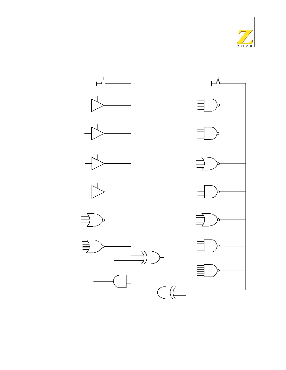
Z8 GP
TM
OTP MCU Family
Product Specification
PS023702-1004
P r e l i m i n a r y Functional
Description
57
Figure 35. Stop Mode Recovery Source
SMR2 D4 D3 D2
1
0 0
SMR2 D4 D3 D2
1 1 1
SMR D4 D3 D2
0
1 0
SMR D4 D3 D2
1 1 1
SMR D4 D3 D2
1
0 1
SMR D4 D3 D2
1
0 0
SMR D4 D3 D2
0
1 1
SMR D4 D3 D2
0 0 0
SMR D4 D3 D2
1 1 0
VCC
P31
P32
P33
P27
P20
P23
P20
P27
SMR2 D4 D3 D2
0
0 1
SMR2 D4 D3 D2
0
0 0
SMR2 D4 D3 D2
0
1 0
SMR2 D4 D3 D2
0
1 1
SMR2 D4 D3 D2
1
0 1
SMR2 D4 D3 D2
1 1 0
VCC
P20
P23
P20
P27
P31
P32
P33
P31
P32
P33
P31
P32
P33
P00
P31
P32
P33
P00
P31
P32
P33
P20
P21
SMR D6
SMR2 D6
To RESET and WDT
Circuitry (Active Low)

Z8 GP
TM
OTP MCU Family
Product Specification
PS023702-1004
P r e l i m i n a r y Functional
Description
58
Any Port 2 bit defined as an output drives the corresponding
input to the default state. For example, if the NOR of P23-P20
is selected as the recovery source and P20 is configured as an
output, the remaining SMR pins (P23-P21) form the NOR
equation. This condition allows the remaining inputs to control
the AND/OR function. Refer to SMR2 register on page 59 for
other recover sources.
Stop Mode Recovery Delay Select (D5)
This bit, if Low, disables the T
POR
delay after Stop Mode Recovery. The default
configuration of this bit is 1. If the "fast" wake up is selected, the Stop Mode
Recovery source must be kept active for at least 5 TpC.
It is recommended that this bit be set to 1 if using a crystal or
resonator clock source. The T
POR
delay allows the clock
source to stabilize before executing instructions.
Stop Mode Recovery Edge Select (D6)
A 1 in this bit position indicates that a High level on any one of the recovery
sources wakes the device from Stop Mode. A 0 indicates Low level recovery. The
default is 0 on POR.
Cold or Warm Start (D7)
This bit is read only. It is set to 1 when the device is recovered from Stop Mode.
The bit is set to 0 when the device reset is other than Stop Mode Recovery (SMR).
Table 19. Stop Mode Recovery Source
SMR:432
Operation
D4
D3
D2
Description of Action
0
0
0
POR and/or external reset recovery
0
0
1
Reserved
0
1
0
P31 transition
0
1
1
P32 transition
1
0
0
P33 transition
1
0
1
P27 transition
1
1
0
Logical NOR of P20 through P23
1
1
1
Logical NOR of P20 through P27
Note:
Note:
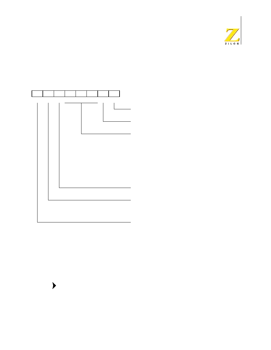
Z8 GP
TM
OTP MCU Family
Product Specification
PS023702-1004
P r e l i m i n a r y Functional
Description
59
Stop Mode Recovery Register 2 (SMR2)
This register determines the mode of Stop Mode Recovery for SMR2 (Figure 36).
SMR2(0F)DH
Figure 36. Stop Mode Recovery Register 2 ((0F)DH:D2≠D4, D6 Write Only)
If SMR2 is used in conjunction with SMR, either of the specified events causes a
Stop Mode Recovery.
Port pins configured as outputs are ignored as an SMR or
SMR2 recovery source. For example, if the NAND or P23≠P20
is selected as the recovery source and P20 is configured as an
output, the remaining SMR pins (P23≠P21) form the NAND
equation.
D7
D6
D5
D4
D3
D2
D1
D0
Reserved (Must be 0)
Reserved (Must be 0)
Stop-Mode Recovery Source 2
000 POR Only *
001 NAND P20, P21, P22, P23
010 NAND P20, P21, P22, P23, P24, P25, P26, P27
011 NOR P31, P32, P33
100 NAND P31, P32, P33
101 NOR P31, P32, P33, P00, P07
110 NAND P31, P32, P33, P00, P07
111 NAND P31, P32, P33, P20, P21, P22
Reserved (Must be 0)
Recovery Level * *
0 Low *
1 High
Reserved (Must be 0)
Note: If used in conjunction with SMR, either of the two specified events causes a Stop-Mode Recovery.
* Default setting after reset
* * At the XOR gate input
Note:

Z8 GP
TM
OTP MCU Family
Product Specification
PS023702-1004
P r e l i m i n a r y Functional
Description
60
Watch-Dog Timer Mode Register (WDTMR)
The Watch-Dog Timer (WDT) is a retriggerable one-shot timer that resets the Z8
Æ
CPU if it reaches its terminal count. The WDT must initially be enabled by execut-
ing the WDT instruction. On subsequent executions of the WDT instruction, the
WDT is refreshed. The WDT circuit is driven by an on-board RC-oscillator. The
WDT instruction affects the Zero (Z), Sign (S), and Overflow (V) flags.
The POR clock source the internal RC-oscillator. Bits 0 and 1 of the WDT register
control a tap circuit that determines the minimum timeout period. Bit 2 determines
whether the WDT is active during HALT, and Bit 3 determines WDT activity during
Stop. Bits 4 through 7 are reserved (Figure 37). This register is accessible only
during the first 60 processor cycles (120 XTAL clocks) from the execution of the
first instruction after Power-On-Reset, Watch-Dog Reset, or a Stop-Mode
Recovery (Figure 36). After this point, the register cannot be modified by any
means (intentional or otherwise). The WDTMR cannot be read. The register is
located in Bank F of the Expanded Register Group at address location
0Fh
. It is
organized as shown in Figure 37.
WDTMR(0F)0Fh
Figure 37. Watch-Dog Timer Mode Register (Write Only)
WDT Time Select (D0, D1)
This bit selects the WDT time period. It is configured as indicated in Table 20.
D7
D6
D5
D4
D3
D2
D1
D0
WDT TAP INT RC OSC
00
5 ms min.
01*
10 ms min.
10
20 ms min.
11
80 ms min.
WDT During HALT
0 OFF
1 ON *
WDT During Stop
0 OFF
1 ON *
Reserved (Must be 0)
* Default setting after reset
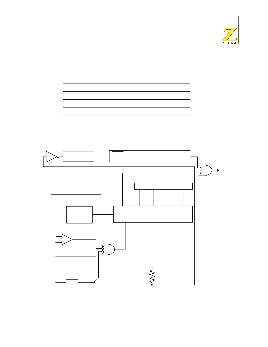
Z8 GP
TM
OTP MCU Family
Product Specification
PS023702-1004
P r e l i m i n a r y Functional
Description
61
WDTMR During Halt (D2)
This bit determines whether or not the WDT is active during HALT Mode. A 1 indi-
cates active during HALT. The default is 1. See Figure 38.
Figure 38. Resets and WDT
Table 20. Watch-Dog Timer Time Select
D1
D0
Timeout of Internal RC-Oscillator
0
0
5ms min.
0
1
10ms min.
1
0
20ms min.
1
1
80ms min.
-
* CLR1 and CLR2 enable the WDT/POR and 18 Clock Reset timers respectively upon a Low-to-High
input translation.
+
From Stop
Mode
Recovery
Source
Stop Delay
Select (SMR)
5 Clock Filter
*CLR2 18 Clock RESET
CLK Generator
RESET
WDT TAP SELECT
POR
5 ms 10 ms 20 ms 80 ms
CLK
*CLR1
WDT/POR Counter Chain
Internal
RC
Oscillator.
WDT
V
DD
Low Operating
Voltage Det.
VBO
V
DD
Internal
RESET
Active
High
12-ns Glitch Filter
XTAL

Z8 GP
TM
OTP MCU Family
Product Specification
PS023702-1004
P r e l i m i n a r y Functional
Description
62
WDTMR During STOP (D3)
This bit determines whether or not the WDT is active during STOP Mode.
Because the XTAL clock is stopped during STOP Mode, the on-board RC has to
be selected as the clock source to the WDT/POR counter. A 1 indicates active
during Stop. The default is 1.
EPROM Selectable Options
There are seven EPROM Selectable Options to choose from based on ROM code
requirements. These options are listed in Table 21.
Voltage Brown-Out/Standby
An on-chip Voltage Comparator checks that the V
DD
is at the required level for
correct operation of the device. Reset is globally driven when V
DD
falls below V
BO
.
A small drop in V
DD
causes the XTAL1 and XTAL2 circuitry to stop the crystal or
resonator clock. If the V
DD
is allowed to stay above V
RAM
, the RAM content is pre-
served. When the power level is returned to above V
BO
, the device performs a
POR and functions normally.
Table 21. EPROM Selectable Options
Port 00≠03 Pull-Ups
On/Off
Port 04≠07 Pull-Ups
On/Off
Port 10≠13 Pull-Ups
On/Off
Port 14≠17 Pull-Ups
On/Off
Port 20≠27 Pull-Ups
On/Off
EPROM Protection
On/Off
Watch-Dog Timer at Power-On Reset On/Off

Z8 GP
TM
OTP MCU Family
Product Specification
PS023702-1004
P r e l i m i n a r y Functional
Description
63
Low-Voltage Detection Register--LVD(D)0Ch
Voltage detection does not work at Stop mode. It must be
disabled during Stop mode in order to reduce current.
Do not modify register P01M while checking a low-voltage
condition. Switching noise of both ports 0 and 1 together might
trigger the LVD flag.
Voltage Detection and Flags
The Voltage Detection register (LVD, register
0CH
at the expanded register bank
0Dh
) offers an option of monitoring the V
CC
voltage. The Voltage Detection is
enabled when bit 0 of LVD register is set. Once Voltage Detection is enabled, the
the V
CC
level is monitored in real time. The flags in the LVD register valid 20uS
after Voltage Detection is enabled. The HVD flag (bit 2 of the LVD register) is set
only if V
CC
is higher than V
HVD.
The LVD flag (bit 1 of the LVD register) is set only
if V
CC
is lower than the V
LVD
. When Voltage Detection is enabled, the LVD flag
also triggers IRQ5. The IRQ bit 5 latches the low voltage condition until it is
cleared by instructions or reset. The IRQ5 interrupt is served if it is enabled in the
IMR register. Otherwise, bit 5 of IRQ register is latched as a flag only.
If it is necessary to receive an LVD interrupt upon power-up at
an operating voltage lower than the low battery detect
threshold, enable interrupts using the Enable Interrupt
instruction (EI) prior to enabling the voltage detection.
Field
Bit Position
Description
LVD
76543---
Reserved
No Effect
-----2--
R
1
0*
HVD flag set
HVD flag reset
------1-
R
1
0*
LVD flag set
LVD flag reset
-------0
R/W 1
0*
Enable VD
Disable VD
*
Default after POR
Note:
Note:
Notes:

Z8 GP
TM
OTP MCU Family
Product Specification
PS023702-1004
P r e l i m i n a r y Expanded Register File Control Registers
64
Expanded Register File Control Registers (0D)
The expanded register file control registers (0D) are depicted in Figure 39 through
Figure 43.
Figure 39. TC8 Control Register ((0D)O0H: Read/Write Except Where Noted)
CTR0(0D)00H
D7
D6
D5
D4
D3
D2
D1
D0
0 P34 as Port Output *
1 Timer8 Output
0 Disable T8 Timeout Interrupt**
1 Enable T8 Timeout Interrupt
0 Disable T8 Data Capture Interrupt**
1 Enable T8 Data Capture Interrupt
00 SCLK on T8**
01 SCLK/2 on T8
10 SCLK/4 on T8
11 SCLK/8 on T8
R 0
No T8 Counter Timeout**
R 1 T8 Counter Timeout Occurred
W 0
No Effect
W 1
Reset Flag to 0
0 Modulo-N*
1 Single Pass
R 0
T8 Disabled *
R 1 T8 Enabled
W 0
Stop T8
W 1
Enable T8
* Default setting after reset
**Default setting after reset. Not reset with Stop Mode recovery.

Z8 GP
TM
OTP MCU Family
Product Specification
PS023702-1004
P r e l i m i n a r y Expanded Register File Control Registers
65
Figure 40. T8 and T16 Common Control Functions ((0D)01H: Read/Write)
CTR1(0D)01H
D7
D6
D5
D4
D3
D2
D1
D0
Transmit Mode*
R/W 0 T16_OUT is 0 initially*
1 T16_OUT is 1 initially
Demodulation Mode
R 0 No Falling Edge Detection
R 1 Falling Edge Detection
W 0 No Effect
W 1 Reset Flag to 0
Transmit Mode*
R/W 0 T8_OUT is 0 initially*
1 T8_OUT is 1 initially
Demodulation Mode
R 0 No Rising Edge Detection
R 1 Rising Edge Detection
W 0 No Effect
W 1 Reset Flag to 0
Transmit Mode*
0 0 Normal Operation*
0 1 Ping-Pong Mode
1 0 T16_OUT = 0
1 1 T16_OUT = 1
Demodulation Mode
0 0 No Filter
0 1 4 SCLK Cycle Filter
1 0 8 SCLK Cycle Filter
1 1 Reserved
Transmit Mode/T8/T16 Logic
0 0 AND**
0 1 OR
1 0 NOR
1 1 NAND
Demodulation Mode
0 0 Falling Edge Detection
0 1 Rising Edge Detection
1 0 Both Edge Detection
1 1 Reserved
Transmit Mode
0 P36 as Port Output *
1 P36 as T8/T16_OUT
Demodulation Mode
0 P31 as Demodulator Input
1 P20 as Demodulator Input
Transmit/Demodulation Mode
0 Transmit Mode *
1 Demodulation Mode
* Default setting after reset
**Default setting after reset. Not reset with Stop Mode
recovery

Z8 GP
TM
OTP MCU Family
Product Specification
PS023702-1004
P r e l i m i n a r y Expanded Register File Control Registers
66
Take care in differentiating the Transmit Mode from
Demodulation Mode. Depending on which of these two modes
is operating, the CTR1 bit has different functions.
Changing from one mode to another cannot be performed
without disabling the counter/timers.
Notes:
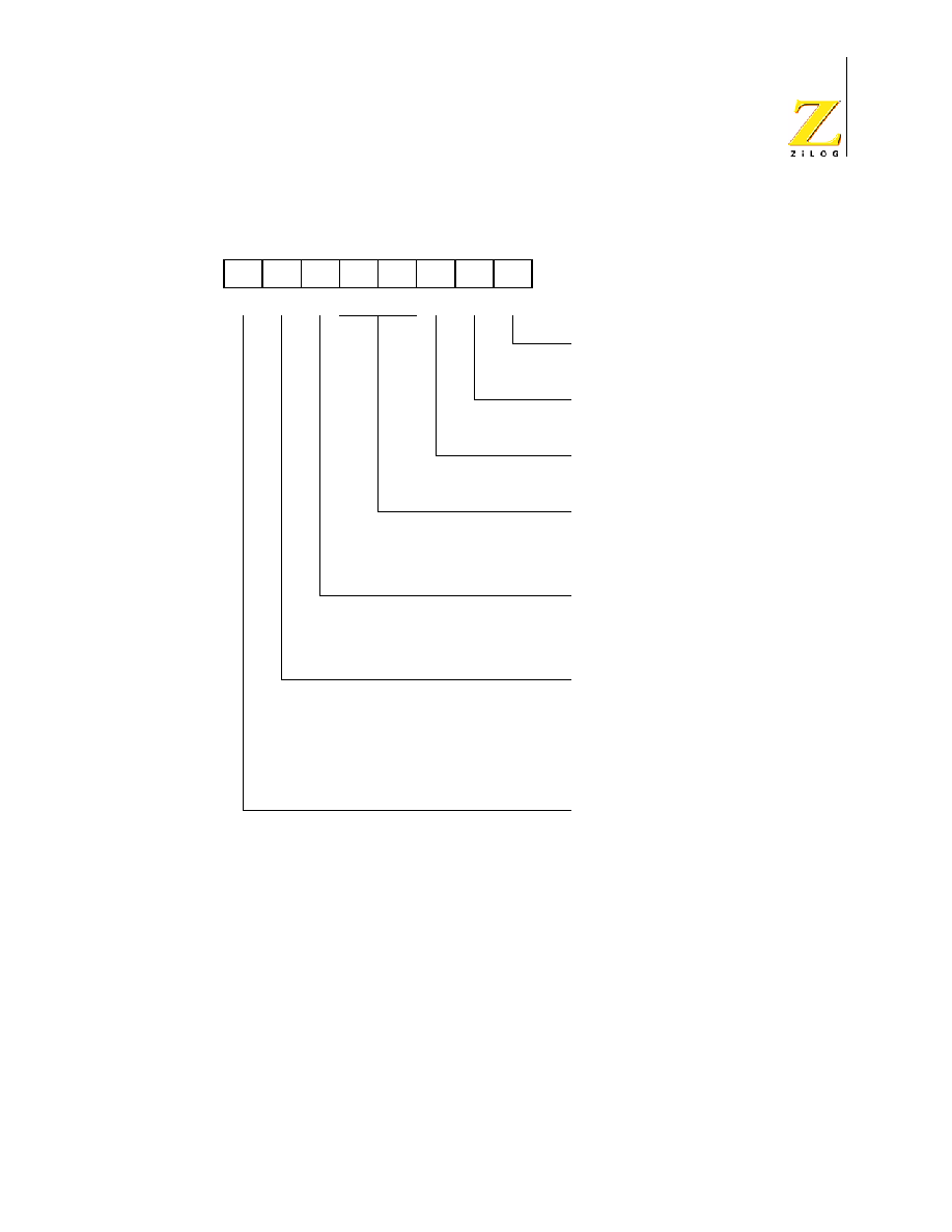
Z8 GP
TM
OTP MCU Family
Product Specification
PS023702-1004
P r e l i m i n a r y Expanded Register File Control Registers
67
CTR2(0D)02H
Figure 41. T16 Control Register ((0D) 2H: Read/Write Except Where Noted)
D7
D6
D5
D4
D3
D2
D1
D0
0 P35 is Port Output *
1 P35 is TC16 Output
0 Disable T16 Timeout Interrupt*
1 Enable T16 Timeout Interrupt
0 Disable T16 Data Capture Interrupt**
1 Enable T16 Data Capture Interrupt
0 0 SCLK on T16**
0 1 SCLK/2 on T16
1 0 SCLK/4 on T16
1 1 SCLK/8 on T16
R 0 No T16 Timeout**
R 1 T16 Timeout Occurs
W 0 No Effect
W 1 Reset Flag to 0
Transmit Mode
0 Modulo-N for T16*
1 Single Pass for T16
Demodulator Mode
0 T16 Recognizes Edge
1 T16 Does Not Recognize Edge
R 0 T16 Disabled *
R 1 T16 Enabled
W 0 Stop T16
W 1 Enable T16
* Default setting after reset
**Default setting after reset. Not reset with Stop
Mode recovery.
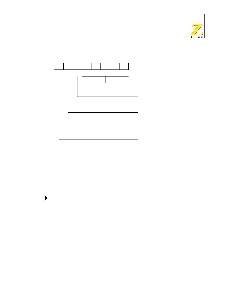
Z8 GP
TM
OTP MCU Family
Product Specification
PS023702-1004
P r e l i m i n a r y Expanded Register File Control Registers
68
CTR3(0D)03H
Figure 42. T8/T16 Control Register (0D)03H: Read/Write (Except Where Noted)
If Sync Mode is enabled, the first pulse of T8 carrier is always
synchronized with T16 (demodulated signal). It can always
provide a full carrier pulse.
D7
D6
D5
D4
D3
D2
D1
D0
Reserved
No effect when written
Always reads
11111
Sync Mode
0* Disable Sync Mode**
1 Enable Sync Mode
T
8
Enable
R 0* T
8
Disabled
R 1 T
8
Enabled
W0 Stop T
8
W1 Enable T
8
T
16
Enable
R 0* T
16
Disabled
R 1 T
16
Enabled
W 0 Stop T
16
W 1 Enable T
16
* Default setting after reset.
** Default setting after reset. Not reset with Stop
Mode recovery.
Note:
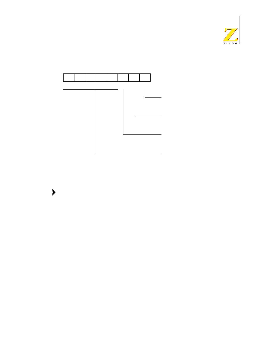
Z8 GP
TM
OTP MCU Family
Product Specification
PS023702-1004
P r e l i m i n a r y Expanded Register File Control Registers
69
LVD(0D)0CH
Figure 43. Voltage Detection Register
Do not modify register P01M while checking a low-voltage
condition. Switching noise of both ports 0 and 1 together might
trigger the LVD flag.
Expanded Register File Control Registers (0F)
The expanded register file control registers (0F) are depicted in Figures 44
through Figure 57.
D7
D6
D5
D4
D3
D2
D1
D0
Voltage Detection
0: Disable *
1: Enable
LVD Flag (Read only)
0: LVD flag reset *
1: LVD flag set
HVD Flag (Read only)
0: HVD flag reset *
1: HVD flag set
Reserved (Must be 0)
* Default
Note:
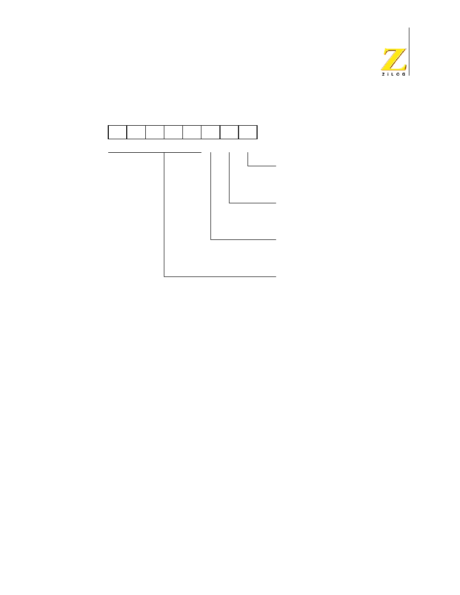
Z8 GP
TM
OTP MCU Family
Product Specification
PS023702-1004
P r e l i m i n a r y Expanded Register File Control Registers
70
PCON(0F)00H
Figure 44. Port Configuration Register (PCON)(0F)00H: Write Only)
D7
D6
D5
D4
D3
D2
D1
D0
Comparator Output Port 3
0 P34, P37 Standard Output *
1 P34, P37 Comparator Output
Port 1
0: Open-Drain
1: Push-Pull*
Port 0
0: Open-Drain
1: Push-Pull *
Reserved (Must be 1)
* Default setting after reset

Z8 GP
TM
OTP MCU Family
Product Specification
PS023702-1004
P r e l i m i n a r y Expanded Register File Control Registers
71
SMR(0F)0BH
Figure 45. Stop Mode Recovery Register ((0F)0BH: D6≠D0=Write Only, D7=Read
Only)
D7
D6
D5
D4
D3
D2
D1
D0
SCLK/TCLK Divide-by-16
0 OFF *
1 ON
Reserved (Must be 0)
Stop-Mode Recovery Source
000 POR Only *
001 Reserved
010 P31
011 P32
100 P33
101 P27
110 P2 NOR 0≠3
111 P2 NOR 0≠7
Stop Delay
0 OFF
1 ON * * * *
Stop Recovery Level * * *
0 Low *
1 High
Stop Flag
0 POR * * * * *
1 Stop Recovery * *
* Default setting after Reset
* * Set after STOP Mode Recovery
* * * At the XOR gate input
* * * * Default setting after Reset. Must be 1 if using a crystal or resonator clock source.
* * * * * Default setting after Power On Reset. Not Reset with a Stop Mode recovery.

Z8 GP
TM
OTP MCU Family
Product Specification
PS023702-1004
P r e l i m i n a r y Expanded Register File Control Registers
72
SMR2(0F)0DH
Figure 46. Stop Mode Recovery Register 2 ((0F)0DH:D2≠D4, D6 Write Only)
D7
D6
D5
D4
D3
D2
D1
D0
Reserved (Must be 0)
Reserved (Must be 0)
Stop-Mode Recovery Source 2
000 POR Only *
001 NAND P20, P21, P22, P23
010 NAND P20, P21, P22, P23, P24, P25, P26, P27
011 NOR P31, P32, P33
100 NAND P31, P32, P33
101 NOR P31, P32, P33, P00, P07
110 NAND P31, P32, P33, P00, P07
111 NAND P31, P32, P33, P20, P21, P22
Reserved (Must be 0)
Recovery Level * *
0 Low
1 High
Reserved (Must be 0)
Note: If used in conjunction with SMR, either of the two specified events causes a Stop-Mode Recovery.
* Default setting after reset
* * At the XOR gate input
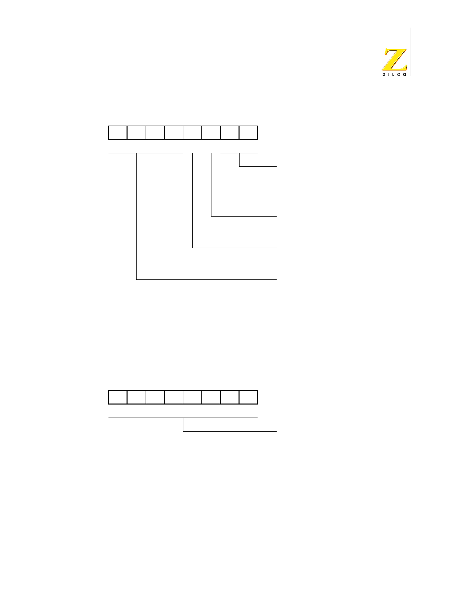
Z8 GP
TM
OTP MCU Family
Product Specification
PS023702-1004
P r e l i m i n a r y
Standard Control Registers
73
WDTMR(0F)0FH
Figure 47. Watch-Dog Timer Register ((0F) 0FH: Write Only)
Standard Control Registers
R246 P2M(F6H)
Figure 48. Port 2 Mode Register (F6H: Write Only)
D7
D6
D5
D4
D3
D2
D1
D0
WDT TAP INT RC OSC
00
5 ms min.
01*
10 ms min.
10
20 ms min.
11
80 ms min.
WDT During HALT
0 OFF
1 ON *
WDT During Stop
0 OFF
1 ON *
Reserved (Must be 0)
* Default setting after reset
D7
D6
D5
D4
D3
D2
D1
D0
P27≠P20 I/O Definition
0 Defines bit as OUTPUT
1 Defines bit as INPUT *
* Default setting after reset

Z8 GP
TM
OTP MCU Family
Product Specification
PS023702-1004
P r e l i m i n a r y
Standard Control Registers
74
R247 P3M(F7H)
Figure 49. Port 3 Mode Register (F7H: Write Only)
D7
D6
D5
D4
D3
D2
D1
D0
0: Port 2 Open Drain *
1: Port 2 Push-Pull
0= P31, P32 Digital Mode*
1= P31, P32 Analog Mode
Reserved (Must be 0)
* Default setting after reset. Not reset with Stop Mode recovery.
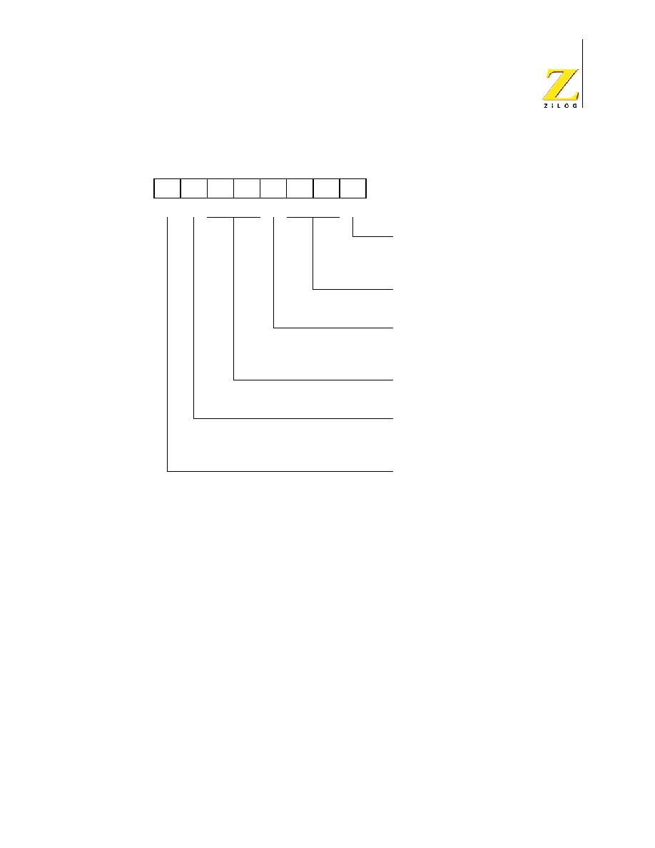
Z8 GP
TM
OTP MCU Family
Product Specification
PS023702-1004
P r e l i m i n a r y
Standard Control Registers
75
R248 P01M(F8H)
Figure 50. Port 0 and 1 Mode Register (F8H: Write Only)
D7
D6
D5
D4
D3
D2
D1
D0
P00≠P03 Mode
0: Output
1: Input *
Reserved (Must be 0)
P17≠P10 Mode
0: Byte Output
1: Byte Input*
Reserved (Must be 0)
P07≠P04 Mode
0: Output
1: Input *
Reserved (Must be 0)
* Default setting after reset; only P00, P01 and P07 are available in 20-pin
configurations.

Z8 GP
TM
OTP MCU Family
Product Specification
PS023702-1004
P r e l i m i n a r y
Standard Control Registers
76
R249 IPR(F9H)
Figure 51. Interrupt Priority Register (F9H: Write Only)
D7
D6
D5
D4
D3
D2
D1
D0
Interrupt Group Priority
000 Reserved
001 C > A > B
010 A > B >C
011 A > C > B
100 B > C > A
101 C > B > A
110 B > A > C
111 Reserved
IRQ1, IRQ4, Priority
(Group C)
0: IRQ1 > IRQ4
1: IRQ4 > IRQ1
IRQ0, IRQ2, Priority
(Group B)
0: IRQ2 > IRQ0
1: IRQ0 > IRQ2
IRQ3, IRQ5, Priority
(Group A)
0: IRQ5 > IRQ3
1: IRQ3 > IRQ5
Reserved; must be 0

Z8 GP
TM
OTP MCU Family
Product Specification
PS023702-1004
P r e l i m i n a r y
Standard Control Registers
77
R250 IRQ(FAH)
Figure 52. Interrupt Request Register (FAH: Read/Write)
R251 IMR(FBH)
Figure 53. Interrupt Mask Register (FBH: Read/Write)
D7
D6
D5
D4
D3
D2
D1
D0
IRQ0 = P32 Input
IRQ1 = P33 Input
IRQ2 = P31 Input
IRQ3 = T16
IRQ4 = T8
IRQ5 = LVD
Inter Edge
P31
P32
= 00
P31
P32
= 01
P31
P32
= 10
P31
P32
= 11
D7
D6
D5
D4
D3
D2
D1
D0
1 Enables IRQ5≠IRQ0
(D0 = IRQ0)
Reserved (Must be 0)
0 Master Interrupt Disable *
1 Master Interrupt Enable * *
* Default setting after reset
* * Only by using EI, DI instruction; DI is required before changing the IMR register

Z8 GP
TM
OTP MCU Family
Product Specification
PS023702-1004
P r e l i m i n a r y
Standard Control Registers
78
R252 Flags(FCH)
Figure 54. Flag Register (FCH: Read/Write)
R253 RP(FDH)
Figure 55. Register Pointer (FDH: Read/Write)
D7
D6
D5
D4
D3
D2
D1
D0
User Flag F1
User Flag F2
Half Carry Flag
Decimal Adjust Flag
Overflow Flag
Sign Tag
Zero Flag
Carry Flag
D7
D6
D5
D4
D3
D2
D1
D0
Expanded Register Bank Pointer
Working Register Pointer
Default setting after reset = 0000 0000
Z8 GP
TM
OTP MCU Family
Product Specification
PS023702-1004
P r e l i m i n a r y
Standard Control Registers
79
R254 SPH(FEH)
Figure 56. Stack Pointer High (FEH: Read/Write)
R255 SPL(FFH)
Figure 57. Stack Pointer Low (FFH: Read/Write)
D7
D6
D5
D4
D3
D2
D1
D0
General-Purpose Register
D7
D6
D5
D4
D3
D2
D1
D0
Stack Pointer Low
Byte (SP7≠SP0)
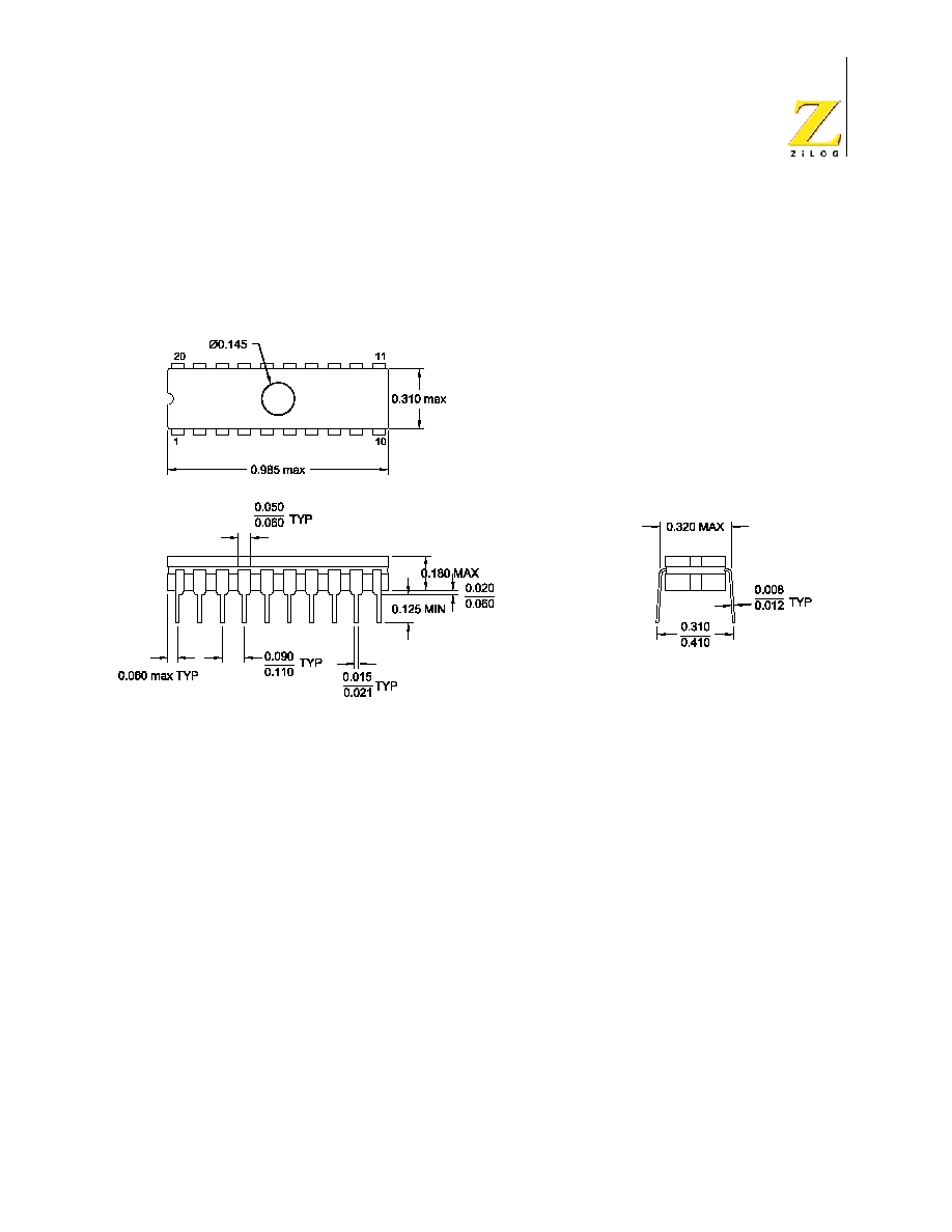
Z8 GP
TM
OTP MCU Family
Product Specification
PS023702-1004
P r e l i m i n a r y Package
Information
80
Package Information
Package information for all versions of Z8 GP
TM
OTP MCU Family are depicted in
Figures 58 through Figure 68.
Figure 58. 20-Pin CDIP Package

Z8 GP
TM
OTP MCU Family
Product Specification
PS023702-1004
P r e l i m i n a r y Package
Information
81
Figure 59. 20-Pin PDIP Package Diagram
Figure 60. 20-Pin SOIC Package Diagram

Z8 GP
TM
OTP MCU Family
Product Specification
PS023702-1004
P r e l i m i n a r y Package
Information
82
Figure 61. 20-Pin SSOP Package Diagram
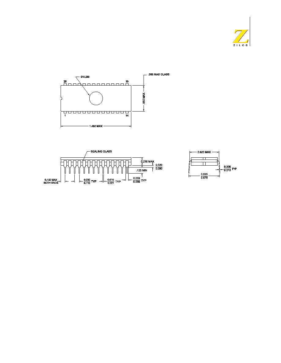
Z8 GP
TM
OTP MCU Family
Product Specification
PS023702-1004
P r e l i m i n a r y Package
Information
83
Figure 62. 28-Pin CDIP Package

Z8 GP
TM
OTP MCU Family
Product Specification
PS023702-1004
P r e l i m i n a r y Package
Information
84
Figure 63. 28-Pin SOIC Package Diagram

Z8 GP
TM
OTP MCU Family
Product Specification
PS023702-1004
P r e l i m i n a r y Package
Information
85
Figure 64. 28-Pin PDIP Package Diagram
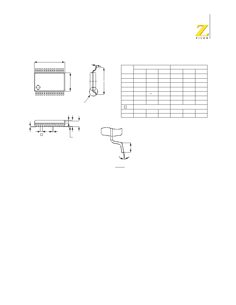
Z8 GP
TM
OTP MCU Family
Product Specification
PS023702-1004
P r e l i m i n a r y Package
Information
86
Figure 65. 28-Pin SSOP Package Diagram
SYMBOL
A
A1
B
C
A2
e
MILLIMETER
INCH
MIN
MAX
MIN
MAX
1.73
0.05
1.68
0.25
5.20
0.65 TYP
0.09
10.07
7.65
0.63
1.86
0.0256 TYP
0.13
10.20
1.73
7.80
5.30
1.99
0.21
1.78
0.75
0.068
0.002
0.066
0.010
0.205
0.004
0.397
0.301
0.025
0.073
0.005
0.068
0.209
0.006
0.402
0.307
0.030
0.078
0.008
0.070
0.015
0.212
0.008
0.407
0.311
0.037
0.38
0.20
10.33
5.38
7.90
0.95
NOM
NOM
D
E
H
L
CONTROLLING DIMENSIONS: MM
LEADS ARE COPLANAR WITHIN .004 INCHES.
H
C
DETAIL A
E
D
28
15
1
14
SEATING PLANE
A2
e
A
Q1
A1
B
L
0 - 8
DETAIL 'A'

Z8 GP
TM
OTP MCU Family
Product Specification
PS023702-1004
P r e l i m i n a r y Package
Information
87
Figure 66. 40-Pin CDIP Package
Figure 67. 40-Pin PDIP Package Diagram

Z8 GP
TM
OTP MCU Family
Product Specification
PS023702-1004
P r e l i m i n a r y Package
Information
88
Figure 68. 48-Pin SSOP Package Design
Check with ZiLOG on the actual bonding diagram and
coordinate for chip-on-board assembly.
CONTROLLING DIMENSIONS : MM
LEADS ARE COPLANAR WITHIN .004 INCH
D
E
H
A1
A2
A
e
SEATING PLANE
b
48
25
c
Detail A
Detail A
0-8∞
L
1
24
Note:

Z8 GP
TM
OTP MCU Family
Product Specification
PS023702-1004
P r e l i m i n a r y Ordering
Information
89
Ordering Information
32KB Standard Temperature: 0∞ to +70∞C
Part Number
Description
Part Number
Description
ZGP323LSH4832C 48-pin SSOP 32K OTP ZGP323LSS2832C 28-pin SOIC 32K OTP
ZGP323LSP4032C 40-pin PDIP 32K OTP
ZGP323LSH2032C 20-pin SSOP 32K OTP
ZGP323LSH2832C 28-pin SSOP 32K OTP ZGP323LSP2032C 20-pin PDIP 32K OTP
ZGP323LSP2832C 28-pin PDIP 32K OTP
ZGP323LSS2032C 20-pin SOIC 32K OTP
ZGP323LSK2032E 20-pin CDIP 32K OTP
ZGP323LSK4032E
40-pin CDIP 32K OTP
ZGP323LSK2832E
28-pin CDIP 32K OTP
32KB Extended Temperature: -40∞ to +105∞C
Part Number
Description
Part Number
Description
ZGP323LEH4832C 48-pin SSOP 32K OTP ZGP323LES2832C 28-pin SOIC 32K OTP
ZGP323LEP4032C 40-pin PDIP 32K OTP
ZGP323LEH2032C 20-pin SSOP 32K OTP
ZGP323LEH2832C 28-pin SSOP 32K OTP ZGP323LEP2032C 20-pin PDIP 32K OTP
ZGP323LEP2832C 28-pin PDIP 32K OTP
ZGP323LES2032C 20-pin SOIC 32K OTP
32KB Automotive Temperature: -40∞ to +125∞C
Part Number
Description
Part Number
Description
ZGP323LAH4832C 48-pin SSOP 32K OTP ZGP323LAS2832C 28-pin SOIC 32K OTP
ZGP323LAP4032C 40-pin PDIP 32K OTP
ZGP323LAH2032C 20-pin SSOP 32K OTP
ZGP323LAH2832C 28-pin SSOP 32K OTP ZGP323LAP2032C 20-pin PDIP 32K OTP
ZGP323LAP2832C 28-pin PDIP 32K OTP
ZGP323LAS2032C 20-pin SOIC 32K OTP
Note: Replace C with G for Lead-Free Packaging

Z8 GP
TM
OTP MCU Family
Product Specification
PS023702-1004
P r e l i m i n a r y Ordering
Information
90
16KB Standard Temperature: 0∞ to +70∞C
Part Number
Description
Part Number
Description
ZGP323LSH4816C 48-pin SSOP 16K OTP ZGP323LSS2816C 28-pin SOIC 16K OTP
ZGP323LSP4016C 40-pin PDIP 16K OTP
ZGP323LSH2016C 20-pin SSOP 16K OTP
ZGP323LSH2816C 28-pin SSOP 16K OTP ZGP323LSP2016C 20-pin PDIP 16K OTP
ZGP323LSP2816C 28-pin PDIP 16K OTP
ZGP323LSS2016C 20-pin SOIC 16K OTP
16KB Extended Temperature: -40∞ to +105∞C
Part Number
Description
Part Number
Description
ZGP323LEH4816C 48-pin SSOP 16K OTP ZGP323LES2816C 28-pin SOIC 16K OTP
ZGP323LEP4016C 40-pin PDIP 16K OTP
ZGP323LES2016C 20-pin SOIC 16K OTP
ZGP323LEH2816C 28-pin SSOP 16K OTP ZGP323LEH2016C 20-pin SSOP 16K OTP
ZGP323LEP2816C 28-pin PDIP 16K OTP
ZGP323LEP2016C 20-pin PDIP 16K OTP
16KB Automotive Temperature: -40∞ to +125∞C
Part Number
Description
Part Number
Description
ZGP323LAH4816C 48-pin SSOP 16K OTP ZGP323LAS2816C 28-pin SOIC 16K OTP
ZGP323LAP4016C 40-pin PDIP 16K OTP
ZGP323LAH2016C 20-pin SSOP 16K OTP
ZGP323LAH2816C 28-pin SSOP 16K OTP ZGP323LAP2016C 20-pin PDIP 16K OTP
ZGP323LAP2816C 28-pin PDIP 16K OTP
ZGP323LAS2016C 20-pin SOIC 16K OTP
Note: Replace C with G for Lead-Free Packaging

Z8 GP
TM
OTP MCU Family
Product Specification
PS023702-1004
P r e l i m i n a r y Ordering
Information
91
8KB Standard Temperature: 0∞ to +70∞C
Part Number
Description
Part Number
Description
ZGP323LSH4808C 48-pin SSOP 8K OTP
ZGP323LSS2808C 28-pin SOIC 8K OTP
ZGP323LSP4008C 40-pin PDIP 8K OTP
ZGP323LSH2008C 20-pin SSOP 8K OTP
ZGP323LSH2808C 28-pin SSOP 8K OTP
ZGP323LSP2008C 20-pin PDIP 8K OTP
ZGP323LSP2808C 28-pin PDIP 8K OTP
ZGP323LSS2008C 20-pin SOIC 8K OTP
8KB Extended Temperature: -40∞ to +105∞C
Part Number
Description
Part Number
Description
ZGP323LEH4808C 48-pin SSOP 8K OTP
ZGP323LES2808C 28-pin SOIC 8K OTP
ZGP323LEP4008C 40-pin PDIP 8K OTP
ZGP323LEH2008C 20-pin SSOP 8K OTP
ZGP323LEH2808C 28-pin SSOP 8K OTP
ZGP323LEP2008C 20-pin PDIP 8K OTP
ZGP323LEP2808C 28-pin PDIP 8K OTP
ZGP323LES2008C 20-pin SOIC 8K OTP
8KB Automotive Temperature: -40∞ to +125∞C
Part Number
Description
Part Number
Description
ZGP323LAH4808C 48-pin SSOP 8K OTP
ZGP323LAS2808C 28-pin SOIC 8K OTP
ZGP323LAP4008C 40-pin PDIP 8K OTP
ZGP323LAH2008C 20-pin SSOP 8K OTP
ZGP323LAH2808C 28-pin SSOP 8K OTP
ZGP323LAP2008C 20-pin PDIP 8K OTP
ZGP323LAP2808C 28-pin PDIP 8K OTP
ZGP323LAS2008C 20-pin SOIC 8K OTP
Note: Replace C with G for Lead-Free Packaging

Z8 GP
TM
OTP MCU Family
Product Specification
PS023702-1004
P r e l i m i n a r y Ordering
Information
92
4KB Standard Temperature: 0∞ to +70∞C
Part Number
Description
Part Number
Description
ZGP323LSH4804C 48-pin SSOP 4K OTP
ZGP323LSS2804C 28-pin SOIC 4K OTP
ZGP323LSP4004C 40-pin PDIP 4K OTP
ZGP323LSH2004C 20-pin SSOP 4K OTP
ZGP323LSH2804C 28-pin SSOP 4K OTP
ZGP323LSP2004C 20-pin PDIP 4K OTP
ZGP323LSP2804C 28-pin PDIP 4K OTP
ZGP323LSS2004C 20-pin SOIC 4K OTP
4KB Extended Temperature: -40∞ to +105∞C
Part Number
Description
Part Number
Description
ZGP323LEH4804C 48-pin SSOP 4K OTP
ZGP323LES2804C 28-pin SOIC 4K OTP
ZGP323LEP4004C 40-pin PDIP 4K OTP
ZGP323LEH2004C 20-pin SSOP 4K OTP
ZGP323LEH2804C 28-pin SSOP 4K OTP
ZGP323LEP2004C 20-pin PDIP 4K OTP
ZGP323LEP2804C 28-pin PDIP 4K OTP
ZGP323LES2004C 20-pin SOIC 4K OTP
4KB Automotive Temperature: -40∞ to +125∞C
Part Number
Description
Part Number
Description
ZGP323LAH4804C 48-pin SSOP 4K OTP
ZGP323LAS2804C 28-pin SOIC 4K OTP
ZGP323LAP4004C 40-pin PDIP 4K OTP
ZGP323LAH2004C 20-pin SSOP 4K OTP
ZGP323LAH2804C 28-pin SSOP 4K OTP
ZGP323LAP2004C 20-pin PDIP 4K OTP
ZGP323LAP2804C 28-pin PDIP 4K OTP
ZGP323LAS2004C 20-pin SOIC 4K OTP
Note: Replace C with G for Lead-Free Packaging
Additional Components
Part Number
Description
Part Number
Description
ZGP323ICE01ZEM Emulator/programmer
ZGP32300100ZPR Programming System

Z8 GP
TM
OTP MCU Family
Product Specification
PS023702-1004
P r e l i m i n a r y Ordering
Information
93
For fast results, contact your local ZiLOG sales office for assistance in ordering
the part desired.
Codes
ZG = ZiLOG General Purpose Family
P = OTP
323 = Family Designation
L = Voltage Range
2V to 3.6V
T = Temperature Range:
S = 0 to 70 degrees C (Standard)
E = -40 to +105 degrees C (Extended)
A = -40 to +125 degrees C (Automotive)
P = Package Type:
K = Windowed Cerdip
P = PDIP
H = SSOP
S = SOIC
## = Number of Pins
CC = Memory Size
M = Packaging Options
C = Non Lead-Free
G = Lead-Free
E = CDIP

Z8 GP
TM
OTP MCU Family
Product Specification
PS023702-1004
P r e l i m i n a r y Ordering
Information
94
Example
ZG
P
323
L
S
P
48
32 G
Lead Free
Memory Size
Number of Pins
Package Type
Temperature Range
Voltage Range
L =2.0V to 3.6V
Family Designation
OTP
ZiLOG General-Purpose Family

Z8 GP
TM
OTP MCU Family
Product Specification
PS023702-1004
P r e l i m i n a r y Precharacterization
Product
95
Precharacterization Product
The product represented by this document is newly introduced and ZiLOG has not
completed the full characterization of the product. The document states what
ZiLOG knows about this product at this time, but additional features or nonconfor-
mance with some aspects of the document might be found, either by ZiLOG or its
customers in the course of further application and characterization work. In addi-
tion, ZiLOG cautions that delivery might be uncertain at times, due to start-up yield
issues.
ZiLOG, Inc.
532 Race Street
San Jose, CA 95126-3432
Telephone: (408) 558-8500
FAX: 408 558-8300
Internet:
http://www.ZiLOG.com

Z8 GP
TM
OTP MCU Family
Product Specification
PS023702-1004
P r e l i m i n a r y Index
96
Index
Numerics
16-bit counter/timer circuits
44
20-pin DIP package diagram
81
20-pin SSOP package diagram
82
28-pin DIP package diagram
85
28-pin SOICpackage diagram
84
28-pin SSOP package diagram
86
40-pin DIP package diagram
87
48-pin SSOP package diagram
88
8-bit counter/timer circuits
40
A
absolute maximum ratings
10
AC
characteristics
14
timing diagram
14
address spaces, basic
2
architecture
2
expanded register file
26
B
basic address spaces
2
block diagram, ZLP32300 functional
3
C
capacitance
11
characteristics
AC
14
DC
11
clock
51
comparator inputs/outputs
23
configuration
port 0
17
port 1
18
port 2
19
port 3
20
port 3 counter/timer
22
counter/timer
16-bit circuits
44
8-bit circuits
40
brown-out voltage/standby
62
clock
51
demodulation mode count capture flow-
chart
42
demodulation mode flowchart
43
EPROM selectable options
62
glitch filter circuitry
38
halt instruction
52
input circuit
38
interrupt block diagram
49
interrupt types, sources and vectors
50
oscillator configuration
51
output circuit
47
ping-pong mode
46
port configuration register
53
resets and WDT
61
SCLK circuit
56
stop instruction
52
stop mode recovery register
55
stop mode recovery register 2
59
stop mode recovery source
57
T16 demodulation mode
45
T16 transmit mode
44
T16_OUT in modulo-N mode
45
T16_OUT in single-pass mode
45
T8 demodulation mode
41
T8 transmit mode
38
T8_OUT in modulo-N mode
41
T8_OUT in single-pass mode
41
transmit mode flowchart
39
voltage detection and flags
63
watch-dog timer mode register
60
watch-dog timer time select
61
CTR(D)01h T8 and T16 Common Functions
33

Z8 GP
TM
OTP MCU Family
Product Specification
PS023702-1004
P r e l i m i n a r y Index
97
D
DC characteristics
11
demodulation mode
count capture flowchart
42
flowchart
43
T16
45
T8
41
description
functional
23
general
2
pin
4
E
EPROM
selectable options
62
expanded register file
24
expanded register file architecture
26
expanded register file control registers
69
flag
78
interrupt mask register
77
interrupt priority register
76
interrupt request register
77
port 0 and 1 mode register
75
port 2 configuration register
73
port 3 mode register
74
port configuration register
73
register pointer
78
stack pointer high register
79
stack pointer low register
79
stop-mode recovery register
71
stop-mode recovery register 2
72
T16 control register
67
T8 and T16 common control functions reg-
ister
65
T8/T16 control register
68
TC8 control register
64
watch-dog timer register
73
F
features
standby modes
1
functional description
counter/timer functional blocks
38
CTR(D)01h register
33
CTR0(D)00h register
31
CTR2(D)02h register
35
CTR3(D)03h register
37
expanded register file
24
expanded register file architecture
26
HI16(D)09h register
30
HI8(D)0Bh register
30
L08(D)0Ah register
30
L0I6(D)08h register
30
program memory map
24
RAM
23
register description
63
register file
28
register pointer
27
register pointer detail
29
SMR2(F)0D1h register
38
stack
29
TC16H(D)07h register
30
TC16L(D)06h register
31
TC8H(D)05h register
31
TC8L(D)04h register
31
G
glitch filter circuitry
38
H
halt instruction, counter/timer
52
I
input circuit
38
interrupt block diagram, counter/timer
49
interrupt types, sources and vectors
50
L
low-voltage detection register
63

Z8 GP
TM
OTP MCU Family
Product Specification
PS023702-1004
P r e l i m i n a r y Index
98
M
memory, program
23
modulo-N mode
T16_OUT
45
T8_OUT
41
O
oscillator configuration
51
output circuit, counter/timer
47
P
package information
20-pin DIP package diagram
81
20-pin SSOP package diagram
82
28-pin DIP package diagram
85
28-pin SOIC package diagram
84
28-pin SSOP package diagram
86
40-pin DIP package diagram
87
48-pin SSOP package diagram
88
pin configuration
20-pin DIP/SOIC/SSOP
5
28-pin DIP/SOIC/SSOP
6
40- and 48-pin
8
40-pin DIP
7
48-pin SSOP
8
pin functions
port 0 (P07 - P00)
16
port 0 (P17 - P10)
17
port 0 configuration
17
port 1 configuration
18
port 2 (P27 - P20)
18
port 2 (P37 - P30)
19
port 2 configuration
19
port 3 configuration
20
port 3 counter/timer configuration
22
reset)
23
XTAL1 (time-based input
16
XTAL2 (time-based output)
16
ping-pong mode
46
port 0 configuration
17
port 0 pin function
16
port 1 configuration
18
port 1 pin function
17
port 2 configuration
19
port 2 pin function
18
port 3 configuration
20
port 3 pin function
19
port 3counter/timer configuration
22
port configuration register
53
power connections
3
power supply
5
precharacterization product
95
program memory
23
map
24
R
ratings, absolute maximum
10
register
59
CTR(D)01h
33
CTR0(D)00h
31
CTR2(D)02h
35
CTR3(D)03h
37
flag
78
HI16(D)09h
30
HI8(D)0Bh
30
interrupt priority
76
interrupt request
77
interruptmask
77
L016(D)08h
30
L08(D)0Ah
30
LVD(D)0Ch
63
pointer
78
port 0 and 1
75
port 2 configuration
73
port 3 mode
74
port configuration
53
,
73
SMR2(F)0Dh
38
stack pointer high
79
stack pointer low
79
stop mode recovery
55
stop mode recovery 2
59
stop-mode recovery
71
stop-mode recovery 2
72
T16 control
67

Z8 GP
TM
OTP MCU Family
Product Specification
PS023702-1004
P r e l i m i n a r y Index
99
T8 and T16 common control functions
65
T8/T16 control
68
TC16H(D)07h
30
TC16L(D)06h
31
TC8 control
64
TC8H(D)05h
31
TC8L(D)04h
31
voltage detection
69
watch-dog timer
73
register description
Counter/Timer2 LS-Byte Hold
31
Counter/Timer2 MS-Byte Hold
30
Counter/Timer8 Control
31
Counter/Timer8 High Hold
31
Counter/Timer8 Low Hold
31
CTR2 Counter/Timer 16 Control
35
CTR3 T8/T16 Control
37
Stop Mode Recovery2
38
T16_Capture_LO
30
T8 and T16 Common functions
33
T8_Capture_HI
30
T8_Capture_LO
30
register file
28
expanded
24
register pointer
27
detail
29
reset pin function
23
resets and WDT
61
S
SCLK circuit
56
single-pass mode
T16_OUT
45
T8_OUT
41
stack
29
standard test conditions
10
standby modes
1
stop instruction, counter/timer
52
stop mode recovery
2 register
59
source
57
stop mode recovery 2
59
stop mode recovery register
55
T
T16 transmit mode
44
T16_Capture_HI
30
T8 transmit mode
38
T8_Capture_HI
30
test conditions, standard
10
test load diagram
10
timing diagram, AC
14
transmit mode flowchart
39
V
VCC
5
voltage
brown-out/standby
62
detection and flags
63
voltage detection register
69
W
watch-dog timer
mode registerwatch-dog timer mode regis-
ter
60
time select
61
X
XTAL1
5
XTAL1 pin function
16
XTAL2
5
XTAL2 pin function
16