 | –≠–ª–µ–∫—Ç—Ä–æ–Ω–Ω—ã–π –∫–æ–º–ø–æ–Ω–µ–Ω—Ç: ASI-SW | –°–∫–∞—á–∞—Ç—å:  PDF PDF  ZIP ZIP |
Rev. 1.6, Copyright © 2002, ZMD AG
All rights reserved. The material contained herein may not be reproduced, adapted, merged, translated, stored, or used without the prior written consent of the copyright owner. The
Information furnished in this publication is preliminary and subject to changes without notice.
1/21
ASI-SW/ASI-SW+
Data Sheet
Low End Device AS-Interface IC
1 Features
∑
Fully operable in AS-interface networking
systems and capable of working in extended net-
works with up to 62 slaves (V2.11)
∑
Dedicated IO-port structure: two data inputs, two
data outputs, no parameter port pins
∑
Integrated EEPROM stores relevant AS-i
information and IC configuration data (e.g. ena-
bling/disabling of the PWM feature)
∑
Programmable PWM of output signals can be
used to control intensity of driven LEDs
2 Description
This integrated circuit shall be used as simplified
interface IC for key control panels, simple sensors
and small actuators based on the AS-i
specifications. The device shall be in compliance
with AS-i Specification V2.11. The IC performs
multiple interface functions.
There are two package options; the 14 pin SOIC
option (ASI-SW) and the 16 pin SOIC option (ASI-
SW+). In contrast to the ASI-SW IC the ASI-SW+
IC has two more pins; a diagnostic LED output pin
(LED pin) and a fault indicator input pin (FID pin).
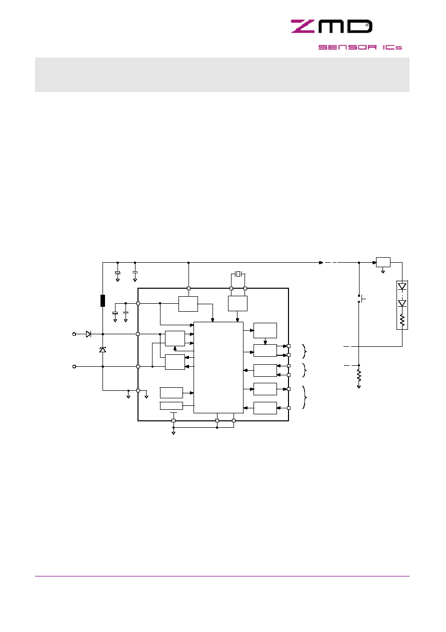
3 Block Diagram
Application
AS-i network
cable access
Oscillator
Pulse
Width
Modulation
Output
Stages
Input
Stages
EEPROM
Thermal
Protection
Receiver
Trans-
mitter
Power
Supply
DIGITAL
LOGIC
UART
State Machine
Ports
Power on
Reset
CAP
ASIP
ASIN
0V
GND
TEST1
TEST2
DI3
DI2
DO1
DO0
OSC1
OSC2
VIN
5V
10uF
24V
16MHz
ASI-SW
ASI-SW+
ASI+
ASI-
Output
Stages
Input
Stages
100nF
LED
FID
diagnostic pins,
available at 16 pin
ASI-SW+ version
only
100nF
1uF
Two inputs, e.g.
interconnced to push
button contacts
Two outputs, e.g.
interconnced to push
button LEDs
Slave electronics
supply voltage
18 mH
Voltage
Regulator
GND
LED-Lamp
Switch
Figure 3-1: Block Diagram

Rev. 1.6, Copyright © 2002, ZMD AG
All rights reserved. The material contained herein may not be reproduced, adapted, merged, translated, stored, or used without the prior written consent of the copyright owner. The
Information furnished in this publication is preliminary and subject to changes without notice.
2/21
ASI-SW/ASI-SW+
Data Sheet
Low End Device AS-Interface IC
1
FEATURES ....................................................................................................................................................1
2
DESCRIPTION ...............................................................................................................................................1
3
BLOCK DIAGRAM .........................................................................................................................................1
4
PIN DESCRIPTION ........................................................................................................................................4
5
PIN CONFIGURATION ..................................................................................................................................4
6
ELECTRICAL SPECIFICATION ....................................................................................................................5
6.1
A
BSOLUTE
M
AXIMUM
R
ATINGS
(N
ON
O
PERATING
) ......................................................................................5
6.2
R
ECOMMENDED
O
PERATING
C
ONDITIONS
...................................................................................................6
6.3
Q
UALITY
A
SSURANCE
................................................................................................................................6
6.4
DC
AND
AC C
HARACTERISTIC OF ALL
P
INS AND
F
UNCTIONS
.......................................................................6
6.4.1
Digital input and output Pins.............................................................................................................7
6.4.2
AS-i Bus Load (Pins ASIP/ASIN and Power Supply Input VIN) .......................................................8
6.4.3
Pins OSC1, OSC2............................................................................................................................8
6.5
I
NFORMATION
D
ATA FOR
D
EVELOPMENT
.....................................................................................................8
7
FUNCTIONAL DESCRIPTION.....................................................................................................................10
7.1
F
UNCTIONAL
B
LOCK
D
IAGRAM
..................................................................................................................10
7.2
P
OWER
S
UPPLY
......................................................................................................................................10
7.3
R
ECEIVER
...............................................................................................................................................10
7.4
T
RANSMITTER
.........................................................................................................................................10
7.5
D
IGITAL
L
OGIC
........................................................................................................................................11
7.6
D
ATA
I/O P
ORTS
.....................................................................................................................................12
7.6.1
Data Exchange Model....................................................................................................................12
7.6.2
PWM Function................................................................................................................................12
7.7
FID I
NPUT AND
LED O
UTPUT
P
ORTS
.......................................................................................................14
8
TYPICAL APPLICATION CIRCUIT OF ASI-SW .........................................................................................15
9
PACKAGE OUTLINE AND DEVICE MARKING..........................................................................................16
10
APPLICATION SUPPORT .......................................................................................................................18
10.1
AS-I
NTERNATIONAL
A
SSOCIATION
........................................................................................................18
10.2
ZMD ...................................................................................................................................................18
10.3
ZMD A
PPLICATION
S
UPPORT
P
ARTNERS
..............................................................................................18
11
SALES CONTACTS .................................................................................................................................18
APPENDIX A:
CRYSTAL PARAMETER ............................................................................................... 19
A.1 P
ARAMETER DATA OF
C
RYSTAL
....................................................................................................................19
A.2 C
APACITANCE ON
PCB ................................................................................................................................19
APPENDIX B:
EXTERNAL COIL ........................................................................................................... 20
B.1
T
ARGET
C
OIL
..........................................................................................................................................20
B.2
C
OIL
M
ODELING
......................................................................................................................................20
APPENDIX C:
EEPROM ........................................................................................................................ 21
Table of Contents
Page

Rev. 1.6, Copyright © 2002, ZMD AG
All rights reserved. The material contained herein may not be reproduced, adapted, merged, translated, stored, or used without the prior written consent of the copyright owner. The
Information furnished in this publication is preliminary and subject to changes without notice.
3/21
ASI-SW/ASI-SW+
Data Sheet
Low End Device AS-Interface IC
Figure 3-1: Block Diagram ....................................................................................................................................1
Figure 5-1: SOIC16 Pin out ...................................................................................................................................4
Figure 5-2: SOIC14 Pin out ...................................................................................................................................5
Figure 6-1: Data Input Schematic in Principle ....................................................................................................7
Figure 6-2: Data Output Schematic in Principle .................................................................................................7
Figure 6-3: Receiver comparator threshold set-up in principle ........................................................................9
Figure 6-4: Reset Behavior ...................................................................................................................................9
Figure 7-1: Functional Block Diagram ...............................................................................................................10
Figure 7-2: ASI-SW IC Data Exchange master call data model .......................................................................12
Figure 7-3: PWM control .....................................................................................................................................13
Figure 7-4: PWM Output Signal Timing .............................................................................................................14
Figure 8-1: Typical Application of ASI-SW IC 14 pin version ..........................................................................15
Figure 8-2: Typical Application of ASI-SW IC 16 pin version ..........................................................................15
Figure 9-1: SOIC Package Outline Dimensions ................................................................................................16
Figure 9-2: Mark Diagram of 14 Pin SOIC Version............................................................................................17
Figure 9-3: Mark Diagram of 16 Pin SOIC Version............................................................................................17
Figure A-1: Crystal oscillator equivalent circuit ...............................................................................................19
Figure B-1: External Coil equivalent circuits ....................................................................................................20
List of Tables
Page
Table 4-1: ASI-SW/ASI-SW+ Pin Description.......................................................................................................4
Table 6-1: Absolute Maximum Ratings................................................................................................................5
Table 6-2: Recommended Operating Conditions ...............................................................................................6
Table 6-3: Crystal Properties
1
...............................................................................................................................6
Table 6-4: Input Voltages and Currents: Pins DI2, DI3, FID, TEST1/2
1
............................................................7
Table 6-5: Output Voltages and Currents: Pins DO0, DO1, LED.......................................................................8
Table 6-6: AS-i Bus Interface Properties .............................................................................................................8
Table 6-7: Oscillator Pins......................................................................................................................................8
Table 6-8: Information Data ..................................................................................................................................8
Table 7-1: ASI-SW Master Calls and Related Slave Responses......................................................................11
Table 7-2: PWM specification of Outputs: Pins DO0, DO1 ..............................................................................13
Table 9-1: Package Outline Dimensions............................................................................................................17
Table A-1: 16 MHz crystals..................................................................................................................................19
Table A-2: Crystal models...................................................................................................................................19
Table C-1: Contents of the ASI-SW EEPROM ...................................................................................................21
Table of Figures
Page
Rev. 1.6, Copyright © 2002, ZMD AG
All rights reserved. The material contained herein may not be reproduced, adapted, merged, translated, stored, or used without the prior written consent of the copyright owner. The
Information furnished in this publication is preliminary and subject to changes without notice.
4/21
ASI-SW/ASI-SW+
Data Sheet
Low End Device AS-Interface IC
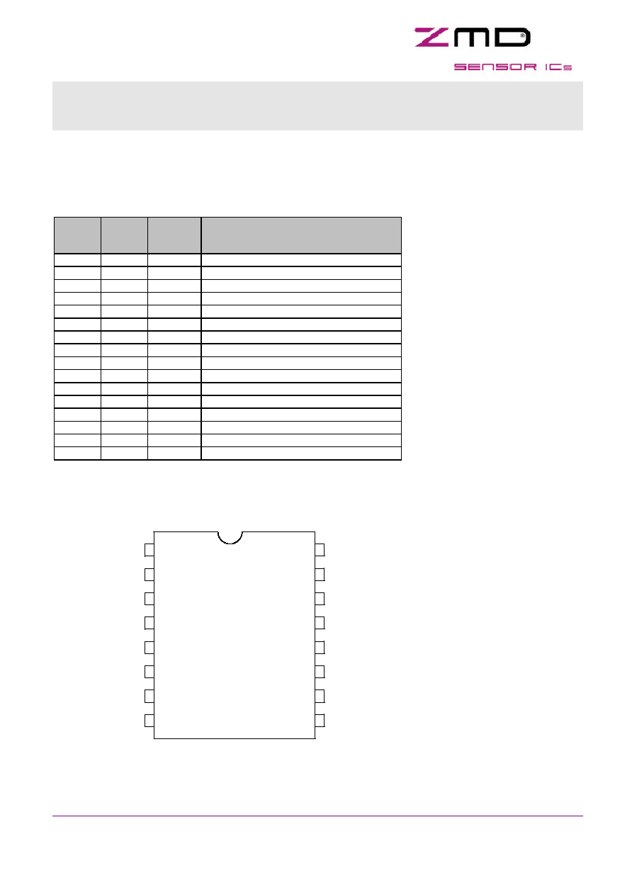
4 Pin Description
Table 4-1 shows the pin description for both the AS-SW and the ASI-SW+ IC. The graphical representation (pin-
out symbols) are shown in chapter 5.
Table 4-1: ASI-SW/ASI-SW+ Pin Description
Pin#
SOIC16
Pin#
SOIC14
Name
Description
1
1
ASIPOS positive ASI supply, high voltage supply
2
2
ASINEG negative ASI supply
3
3
TEST1
test mode input/output
4
4
TEST2
test mode input
5
FID
digital input
6
5
DI2
digital input
7
6
DI3
digital input
8
7
OSC1
crystal oscillator input
9
8
OSC2
crystal oscillator output
10
9
DO1
digital output
11
10
DO0
digital output
12
LED
digital output
13
11
GND
digital ground
14
12
CAP
regulator output
15
13
0V
analog ground
16
14
VIN
High voltage supply
5 Pin Configuration
There is only one die used for both the 14- and 16-pin-version of the ASI-SW. In the 14-pin-version, the internal
ports FID and LED are not bonded to external pins.
ASIPOS
ASINEG
TEST1
TEST2
FID
DI2
DI3
OSC1
VIN
0V
CAP
GND
LED
DO0
DO1
OSC2
1
2
3
4
5
6
7
8
9
10
11
12
13
14
15
16
ASI-SW+
Figure 5-1: SOIC16 Pin out
Rev. 1.6, Copyright © 2002, ZMD AG
All rights reserved. The material contained herein may not be reproduced, adapted, merged, translated, stored, or used without the prior written consent of the copyright owner. The
Information furnished in this publication is preliminary and subject to changes without notice.
5/21
ASI-SW/ASI-SW+
Data Sheet
Low End Device AS-Interface IC
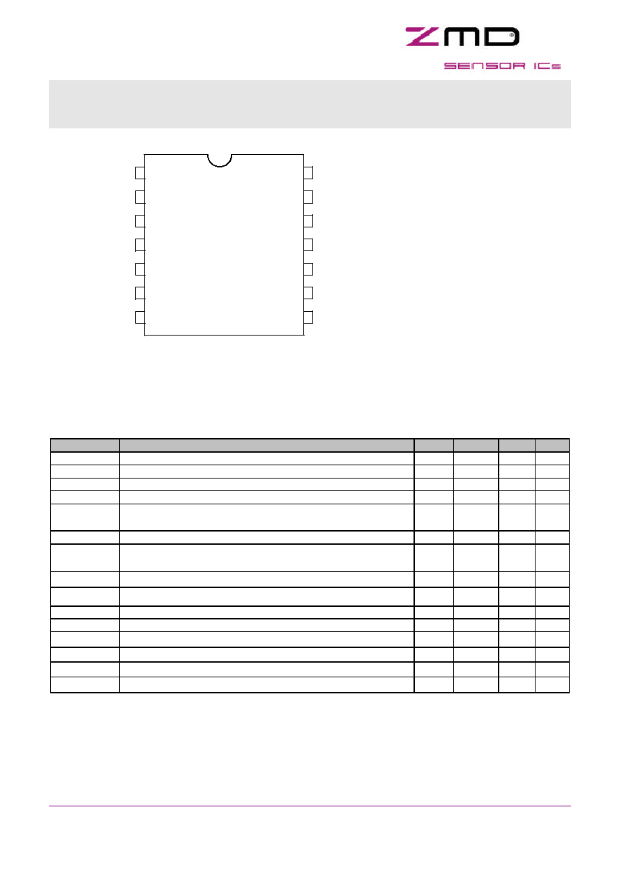
6 Electrical Specification
6.1 Absolute Maximum Ratings (Non Operating)
Table 6-1: Absolute Maximum Ratings
Symbol
Parameter
min
max.
Unit
Note
V0V ,VGND Voltage reference
0
0
V
VASIP
Positive AS-i supply voltage
-0.3
40
V
VASIN
Negative AS-i supply voltage
-0.3
20
V
1
VASIP-ASIN Voltage difference from ASIP to ASIN (V
ASIP
- V
ASIN
)
-0.3
40
V
2
VASIPP
AS-i supply pulse voltage, voltage difference between pins
ASIP and ASIN (from ASIP to ASIN)
50
V
3
VVIN
Power supply input voltage
-0.3
40
V
Vinputs1
Voltage at pins DI2, DI3, DO0, DO1, LED, FID
-0.3
VVIN +
0.3
V
Vinputs2
Voltage at pins OSC1, OSC2, CAP, TEST1, TEST2
-0.3
7
V
Iin
Input current into any pin except supply pins
-25
25
mA
H
Humidity non-condensing
4
VHBM1
Electrostatic discharge ≠ human body model (HBM1)
4000
V
5
VHBM2
Electrostatic discharge ≠ human body model (HBM2)
2000
V
6
VEDM
Electrostatic discharge ≠ equipment discharge model (EDM)
400
V
7
T
STG
Storage temperature
-55
125
∞C
Ptot
Total power dissipation
TBD
W
8
1
ASIN-pin shall be shorted to the 0V and GND pin on the PCB
2
reverse polarity protection has to be performed externally
3
pulse with =< 50us, repetition rate =< 0.5 Hz
4
defined in DIN 40040 cond. F
5
HBM1: C = 100pF charged to V
HBM1
with resistor R = 1.5kOhm in series, valid for ASIP-ASIN only.
6
HBM2: C = 100pF charged to V
HBM2
with resistor R = 1.5kOhm in series, valid for all pins except ASIP-ASIN
7
EDM: C = 200pF charged to V
EDM
with no resistor in series, valid for ASIP-ASIN only
8
at max. operating temperature, the allowed total power dissipation depends on the additional thermal resistance from case to ambient and
on the operation ambient temperature (derating function TBD).
ASIPOS
ASINEG
TEST1
TEST2
DI2
DI3
OSC1
VIN
0V
CAP
GND
DO0
DO1
OSC2
1
2
3
4
5
6
7
8
9
10
11
12
13
14
ASI-SW
Figure 5-2: SOIC14 Pin out