 | –≠–ª–µ–∫—Ç—Ä–æ–Ω–Ω—ã–π –∫–æ–º–ø–æ–Ω–µ–Ω—Ç: U621708 | –°–∫–∞—á–∞—Ç—å:  PDF PDF  ZIP ZIP |
1
November 03, 2003
U621708
Preliminary
!
131072 x 8 bit static CMOS RAM
!
70 ns Access Time
!
Common data inputs and
data outputs
!
Three-state outputs
!
Typ. operating supply current
70 ns: 45mA
!
Standby current <100µA at 85∞C
!
TTL/CMOS-compatible
!
Power supply voltage 5 V
!
Operating temperature range
0 ∞C to 70∞C
-40 ∞C to 85 ∞C
!
QS 9000 Quality Standard
!
ESD protection > 2000 V
(MIL STD 883C M3015.7)
!
Latch-up immunity >100 mA
!
Package: SOP32 (450 mil)
TSOP I 32
sTSOP I 32
The U621708 is a static RAM
manufactured using a CMOS pro-
cess technology with the following
operating modes:
- Read
- Standby
- Write
- Data Retention
The memory array is based on a
6-Transistor cell.
The circuit is activated by the rising
edge of E2 (at E1 = L), or the falling
edge of E1 (at E2 = H). The
address and control inputs open
simultaneously. According to the
information of W and G, the data
inputs, or outputs, are active.
During the active state (E1 = L and
E2 = H) each address change
leads to a new Read cycle. In a
Read cycle, the data outputs are
activated by the falling edge of G,
afterwards the data word will be
available at the outputs DQ0-DQ7.
After the address change, the data
outputs go High-Z until the new
information is available. The data
outputs have no preferred state. If
the memory is driven by CMOS
levels in the active state, and if
there is no change of the address,
data input and control signals W or
G, the operating current (I
O
= 0 mA)
drops to the value of the operating
current in the Standby mode. The
Read cycle is finished by the falling
edge of E2 or W, or by the rising
edge of E1, respectively.
Data retention is guaranteed down
to 2 V. With the exception of E1
and E2, all inputs consist of NOR
gates, so that no pull-up/pull-down
resistors are required.
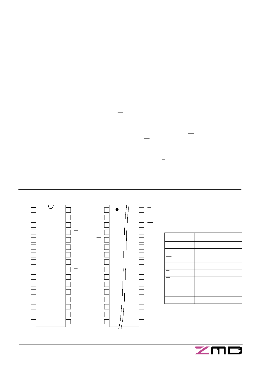
128K x 8 SRAM
Pin Configuration
Top View
Signal Name Signal Description
A0 - A16
Address Inputs
DQ0 - DQ7
Data In/Out
E1
Chip Enable 1
E2
Chip Enable 2
G
Output Enable
W
Write Enable
VCC
Power Supply Voltage
VSS
Ground
n.c.
not connected
Pin Description
1
n.c.
VCC
32
2
A16
A15
31
4
A12
W
29
5
A7
A13
28
3
A14
E2
30
6
A6
A8
27
7
A5
A9
26
8
A4
A11
25
12
A0
DQ7
21
9
A3
G
24
10
A2
A10
23
11
A1
E1
22
13
DQ0
DQ6
20
14
DQ1
DQ5
19
SOP
DQ4
DQ3
DQ2
VSS
18
17
15
16
Description
Features
Top View
1
A11
G
32
2
A9
A10
31
4
A13
DQ7
29
5
W
DQ6
28
3
A8
E1
30
6
E2
DQ5
27
7
A15
DQ4
26
8
VCC
DQ3
25
12
A12
DQ0
21
9
n.c.
VSS
24
10
A16
DQ2
23
11
A14
DQ1
22
13
A7
A0
20
14
A6
A1
19
A2
A3
A5
A4
18
17
15
16
TSOP
sTSOP
2
November 03, 2003
U621708
Preliminary
* H or L
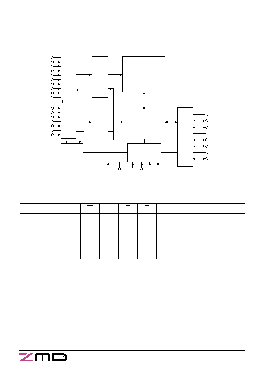
Operating Mode
E1
E2
W
G
DQ0 - DQ7
Standby/not selected
*
L
*
*
High-Z
H
*
*
*
High-Z
Internal Read
L
H
H
H
High-Z
Read L
H
H
L
Data
Outputs
Low-Z
Write
L
H
L
*
Data Inputs High-Z
Truth Table
Block Diagram
DQ0
DQ1
DQ2
DQ3
DQ4
DQ5
DQ6
DQ7
V
CC
V
SS
W
G
E1
Ro
w A
d
d
r
e
s
s
In
p
u
t
s
Co
l
u
m
n
A
d
d
r
e
s
s
In
p
u
ts
Address
Change
Detector
Co
l
u
m
n
De
c
o
d
e
r
Ro
w De
c
o
d
e
r
Sense Amplifier/
Write Control Logic
Co
m
m
o
n
Da
t
a
I
/
O
Memory Cell
Array
1024 Rows x
128 x 8 Columns
A10
A11
A12
A13
A14
A9
A15
A0
A1
A2
A3
A4
A5
A6
A7
A8
A16
E2
Clock
Generator
3
November 03, 2003
U621708
Preliminary
a
Stresses greater than those listed under ,,Absolute Maximum Ratings" may cause permanent damage to the device. This is a stress rating
only, and functional operation of the device at condition above those indicated in the operational sections of this specification is not implied.
Exposure to absolute maximum rating conditions for extended periods may affect reliability
b
Maximum voltage is 7 V
c
Not more than 1 output should be shorted at the same time. Duration of the short circuit should not exceed 30 s.
Absolute Maximum Ratings
a
Symbol
Min.
Max.
Unit
Power Supply Voltage
V
CC
-0.5
7
V
Input Voltage
V
I
-0.5
V
CC
+ 0.5
b
V
Output Voltage
V
O
-0.5
V
CC
+ 0.5
b
V
Power Dissipation
P
D
-
1
W
Operating Temperature
C-Type
K-Type
T
a
0
-40
70
85
∞C
Storage Temperature
T
stg
-65
150
∞C
Output Short-Circuit Current
at V
CC
= 5 V and V
O
= 0 V
c
| I
OS
|
200
mA
Characteristics
All voltages are referenced to V
SS
= 0 V (ground).
All characteristics are valid in the power supply voltage range and in the operating temperature range specified.
Dynamic measurements are based on a rise and fall time of
5 ns, measured between 10 % and 90 % of V
I
, as well as
input levels of V
IL
= 0 V and V
IH
= 3 V. The timing reference level of all input and output signals is 1.5 V,
with the exception of the t
dis
-times and t
en
-times, in which cases transition is measured ±200 mV from steady-state voltage.
d
-2 V at Pulse Width 10 ns
Recommended
Operating Conditions
Symbol
Conditions
Min.
Max.
Unit
Power Supply Voltage
V
CC
4.5
5.5
V
Input Low Voltage
*
V
IL
-0.3
0.8
V
Input High Voltage
V
IH
2.2
V
CC
+ 0.3
V
4
November 03, 2003
U621708
Preliminary
Electrical Characteristics
Symbol
Conditions
Min.
Max.
Unit
Supply Current - Operating Mode
Supply Current - Standby Mode
(CMOS level)
Supply Current - Standby Mode
(TTL level)
I
CC(OP)
I
CC(SB)
I
CC(SB)1
V
CC
V
IL
V
IH
V
CC
V
E1
= V
E2
V
CC
V
E1
= V
E2
= 5.5 V
= 0.8 V
= 2.2 V
= 5.5 V
= V
CC
- 0.2 V
= 5.5 V
= 2.2 V
30
100
10
mA
µA
mA
Output High Voltage
Output Low Voltage
V
OH
V
OL
V
CC
I
OH
V
CC
I
OL
= 4.5 V
= -4.0 mA
= 4.5 V
= 8.0 mA
2.4
0.4
V
V
Input High Leakage Current
Input Low Leakage Current
I
IH
I
IL
V
CC
V
IH
V
CC
V
IL
= 5.5 V
= 5.5 V
= 5.5 V
= 0 V
-2
2
µA
µA
Output High Current
Output Low Current
I
OH
I
OL
V
CC
V
OH
V
CC
V
OL
= 4.5 V
= 2.4 V
= 4.5 V
= 0.4 V
8
-4
mA
mA
Output Leakage Current
High at Three-State Outputs
Low at Three-State Outputs
I
OHZ
I
OLZ
V
CC
V
OH
V
CC
V
OL
= 5.5 V
= 5.5 V
= 5.5 V
=
0 V
-2
2
µA
µA
5
November 03, 2003
U621708
Preliminary
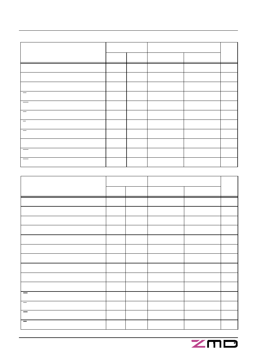
Switching Characteristics
Read Cycle
Symbol
70
Unit
Alt.
IEC
Min.
Max.
Read Cycle Time
t
RC
t
cR
70
ns
Address Access Time to Data Valid
t
AA
t
a(A)
70
ns
Chip Enable Access Time to Data Valid
t
ACE
t
a(E)
70
ns
G LOW to Data Valid
t
OE
t
a(G)
25
ns
E1 HIGH or E2 LOW to Output in High-Z
t
HZCE
t
dis(E)
15
ns
G HIGH to Output in High-Z
t
HZOE
t
dis(G)
15
ns
E1 LOW or E2 HIGH to Output in Low-Z
t
LZCE
t
en(E)
10
ns
G LOW to Output in Low-Z
t
LZOE
t
en(G)
5
ns
Output Hold Time from Address Change
t
OH
t
v(A)
10
ns
E1 LOW or E2 HIGH to Power-Up Time
t
PU
0
ns
E1 HIGH or E2 LOW to Power-Down Time
t
PD
70
ns
Switching Characteristics
Write Cycle
Symbol
70
Unit
Alt.
IEC
Min.
Max.
Write Cycle Time
t
WC
t
cW
70
ns
Write Pulse Width
t
WP
t
w(W)
35
ns
Write Setup Time
t
WP
t
su(W)
35
ns
Address Setup Time
t
AS
t
su(A)
0
ns
Address Valid to End of Write
t
AW
t
su(A-WH)
35
ns
Chip Enable Setup Time
t
CW
t
su(E)
40
ns
Pulse Width Chip Enable to End of Write
t
CW
t
w(E)
40
ns
Data Setup Time
t
DS
t
su(D)
25
ns
Data Hold Time
t
DH
t
h(D)
0
ns
Address Hold from End of Write
t
AH
t
h(A)
0
ns
W LOW to Output in High-Z
t
HZWE
t
dis(W)
20
ns
G HIGH to Output in High-Z
t
HZOE
t
dis(G)
15
ns
W HIGH to Output in Low-Z
t
LZWE
t
en(W)
5
ns
G LOW to Output in Low-Z
t
LZOE
t
en(G)
5
ns