 | –≠–ª–µ–∫—Ç—Ä–æ–Ω–Ω—ã–π –∫–æ–º–ø–æ–Ω–µ–Ω—Ç: U62H256S | –°–∫–∞—á–∞—Ç—å:  PDF PDF  ZIP ZIP |
1
March 8, 1999
U62H256S
Features
F
32768 x 8 bit static CMOS RAM
F
35 and 55 ns Access Time
F
Common data inputs and
data outputs
F
Three-state outputs
F
Typ. operating supply current
35 ns: 45mA
55 ns: 30mA
F
Standby current < 2 mA
F
TTL/CMOS-compatible
F
Automatic reduction of power
dissipation in long Read or Write
cycles
F
Power supply voltage 5 V
F
Operating temperature range
-40
∞
C
to 85
∞
C
-40
∞
C to 125
∞
C
F
CECC 90000 Quality Standard
F
ESD protection > 2000 V
(MIL STD 883C M3015.7)
F
Latch-up immunity >100 mA
F
Package:
SOP28 (300 mil)
Description
The U62H256S is a static RAM
manufactured using a CMOS pro-
cess technology with the following
operating modes:
- Read
- Standby
- Write
- Data Retention
The memory array is based on a
MIXMOS cell.
The circuit is activated by the fal-
ling edge of E. The address and
control inputs open simultaneously.
According to the information of W
and G, the data inputs, or outputs,
are active. During the active state
E = L each address change leads
to a new Read or Write cycle. In a
Read cycle, the data outputs are
activated by the falling edge of G,
afterwards the data word will be
available at the outputs DQ0-DQ7.
After the address change, the data
outputs go High-Z until the new
information is available. The data
outputs have no preferred state. If
the memory is driven by CMOS
levels in the active state, and if
there is no change of the address,
data input and control signals W or
G, the operating current (I
O
= 0 mA)
drops to the value of the operating
current in the Standby mode. The
Read cycle is finished by the falling
edge of W, or by the rising edge of
E, respectively.
Data retention is guaranteed down
to 2 V. With the exception of E, all
inputs consist of NOR gates, so
that no pull-up/pull-down resistors
are required.
Automotive Fast 32K x 8 SRAM
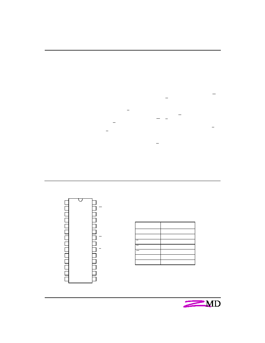
Pin Configuration
Top View
Signal Name
Signal Description
A0 - A14
Address Inputs
DQ0 - DQ7
Data In/Out
E
Chip Enable
G
Output Enable
W
Write Enable
VCC
Power Supply Voltage
VSS
Ground
Pin Description
1
A14
VCC
28
2
A12
W
27
4
A6
A8
25
5
A5
A9
24
3
A7
A13
26
6
A4
A11
23
7
A3
G
22
8
A2
A10
21
12
DQ1
DQ5
17
9
A1
E
20
10
A0
DQ7
19
11
DQ0
DQ6
18
13
DQ2
DQ4
16
14
VSS
DQ3
15
SOP
2
March 8, 1999
U62H256S
* H or L
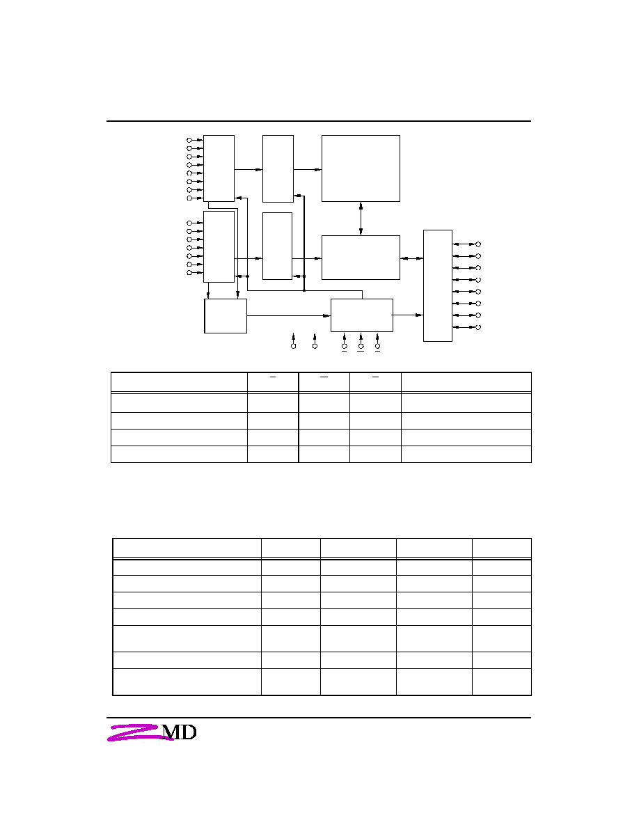
Operating Mode
E
W
G
DQ0 - DQ7
Standby/not selected
H
*
*
High-Z
Internal Read
L
H
H
High-Z
Read
L
H
L
Data Outputs Low-Z
Write
L
L
*
Data Inputs High-Z
Truth Table
Block Diagram
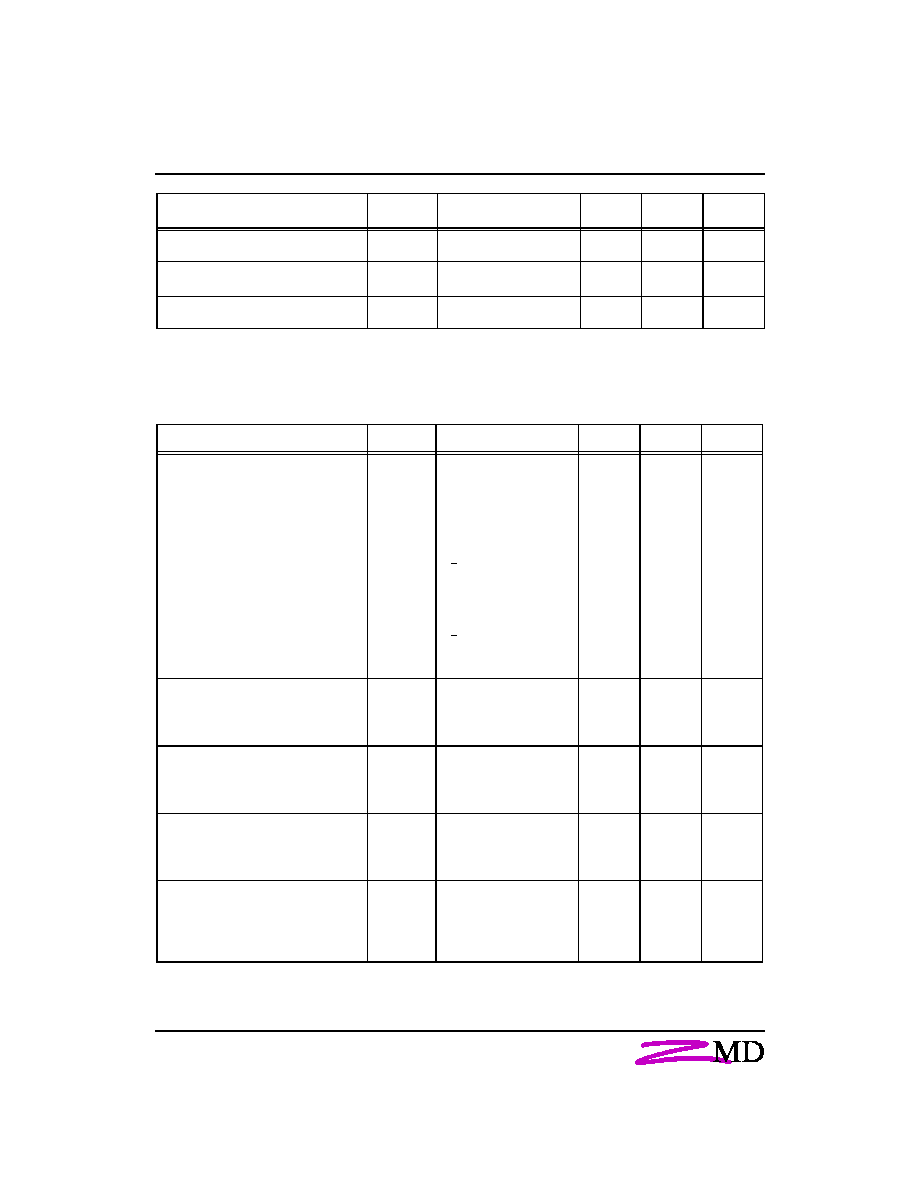
Maximum Ratings
Symbol
Min.
Max.
Unit
Power Supply Voltage
V
CC
-0.5
7
V
Input Voltage
V
I
-0.5
V
CC
+ 0.5
V
Output Voltage
V
O
-0.5
V
CC
+ 0.5
V
Power Dissipation
P
D
-
1
W
Operating Temperature
K-Type
A-Type
T
a
-40
-40
85
125
∞
C
Storage Temperature
T
stg
-65
150
∞
C
Output Short-Circuit Current
at V
CC
= 5 V and V
O
= 0 V
**
| I
OS
|
200
mA
Characteristics
**
Not more than 1 output should be shorted at the same time. Duration of the short circuit should not exceed 30 s.
All voltages are referenced to V
SS
= 0 V (ground).
All characteristics are valid in the power supply voltage range and in the operating temperature range specified.
Dynamic measurements are based on a rise and fall time of
5 ns, measured between 10 % and 90 % of V
I
, as well as
input levels of V
IL
= 0 V and V
IH
= 3 V. The timing reference level of all input and output signals is 1.5 V,
with the exception of the t
dis
-times and t
en
-times, in which cases transition is measured
±
200 mV from steady-state voltage.
DQ0
DQ1
DQ2
DQ3
DQ4
DQ5
DQ6
DQ7
V
CC
V
SS
W
G
E
Ro
w A
d
d
r
e
s
s
I
npu
t
s
Co
lu
m
n
A
d
d
r
e
s
s
I
nput
s
Address
Change
Detector
Co
lu
mn
De
c
o
d
e
r
Ro
w D
e
c
o
d
e
r
Sense Amplifier/
Write Control Logic
Clock
Generator
Co
mmo
n
Da
t
a
I
/
O
Memory Cell
Array
256 Rows x
128 x 8 Columns
A0
A1
A2
A3
A10
A5
A6
A7
A8
A9
A4
A11
A12
A13
A14
3
March 8, 1999
U62H256S
* -2 V at Pulse Width 10 ns
Recommended
Operating Conditions
Symbol
Conditions
Min.
Max.
Unit
Power Supply Voltage
V
CC
4.5
5.5
V
Input Low Voltage
*
V
IL
-0.3
0.8
V
Input High Voltage
V
IH
2.2
V
CC
+ 0.3
V
Electrical Characteristics
Symbol
Conditions
Min.
Max.
Unit
Supply Current - Operating Mode
Supply Current - Standby Mode
(CMOS level)
Supply Current - Standby Mode
(TTL level)
I
CC(OP)
I
CC(SB)
I
CC(SB)1
V
CC
V
IL
V
IH
t
cW
t
cW
V
CC
V
E
K-Type
A-Type
V
CC
V
E
K-Type
A-Type
= 5.5 V
= 0.8 V
= 2.2 V
= 35 ns
= 55 ns
= 5.5 V
= V
CC
- 0.2 V
= 5.5 V
= 2.2 V
90
70
0.5
2
10
20
mA
mA
mA
mA
mA
mA
Output High Voltage
Output Low Voltage
V
OH
V
OL
V
CC
I
OH
V
CC
I
OL
= 4.5 V
= -4.0 mA
= 4.5 V
= 8.0 mA
2.4
0.4
V
V
Input High Leakage Current
Input Low Leakage Current
I
IH
I
IL
V
CC
V
IH
V
CC
V
IL
= 5.5 V
= 5.5 V
= 5.5 V
= 0 V
-2
2
µ
A
µ
A
Output High Current
Output Low Current
I
OH
I
OL
V
CC
V
OH
V
CC
V
OL
= 4.5 V
= 2.4 V
= 4.5 V
= 0.4 V
8
-4
mA
mA
Output Leakage Current
High at Three-State Outputs
Low at Three-State Outputs
I
OHZ
I
OLZ
V
CC
V
OH
V
CC
V
OL
= 5.5 V
= 5.5 V
= 5.5 V
=
0 V
-2
2
µ
A
µ
A
4
March 8, 1999
U62H256S
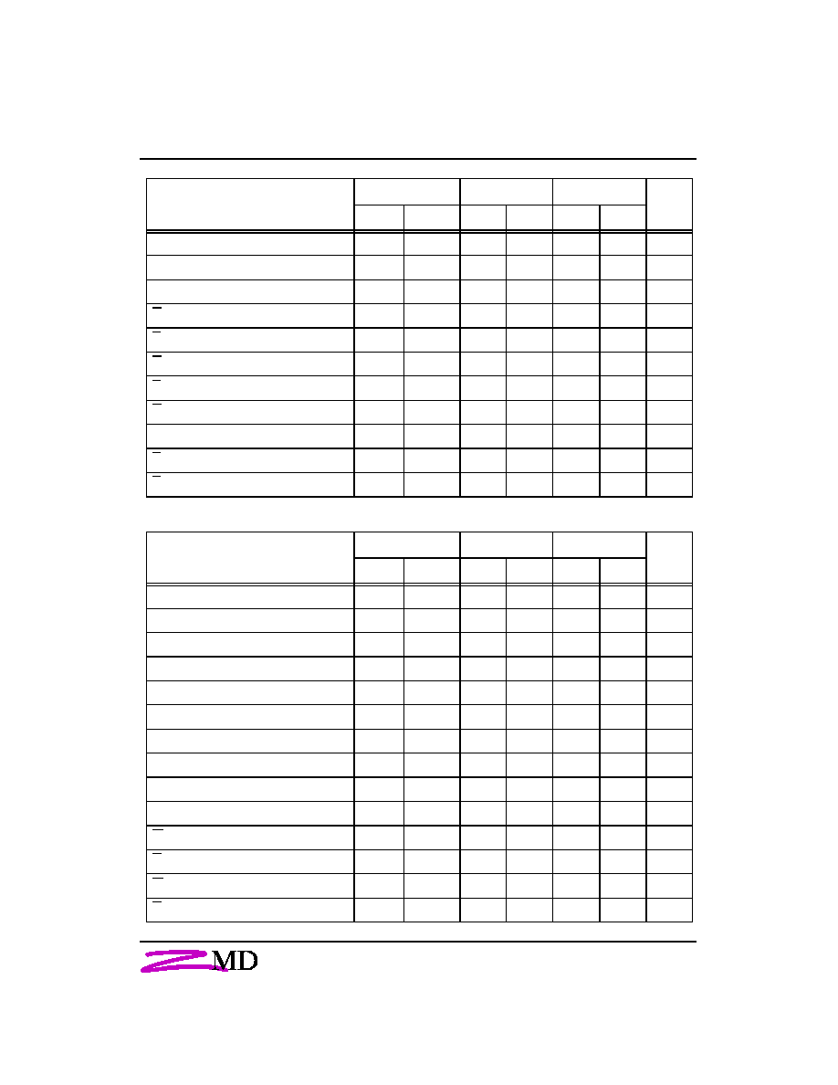
Switching Characteristics
Read Cycle
Symbol
35
55
Unit
Alt.
IEC
Min.
Max.
Min.
Max.
Read Cycle Time
t
RC
t
cR
35
55
ns
Address Access Time to Data Valid
t
AA
t
a(A)
35
55
ns
Chip Enable Access Time to Data Valid
t
ACE
t
a(E)
35
55
ns
G LO W to Data Valid
t
OE
t
a(G)
15
25
ns
E HIGH to Output in High-Z
t
HZCE
t
dis(E)
12
15
ns
G HIGH to Output in High-Z
t
HZOE
t
dis(G)
12
15
ns
E LOW to Output in Low-Z
t
LZCE
t
en(E)
3
3
ns
G LO W to Output in Low-Z
t
LZOE
t
en(G)
0
0
ns
Output Hold Time from Address Change
t
OH
t
v(A)
3
3
ns
E LOW to Power-Up Time
t
PU
0
0
ns
E HIGH to Power-Down Time
t
PD
35
55
ns
Switching Characteristics
Write Cycle
Symbol
35
55
Unit
Alt.
IEC
Min.
Max.
Min.
Max.
Write Cycle Time
t
WC
t
cW
35
55
ns
Write Pulse Width
t
WP
t
w(W)
20
35
ns
Write Setup Time
t
WP
t
su(W)
20
35
ns
Address Setup Time
t
AS
t
su(A)
0
0
ns
Address Valid to End of Write
t
AW
tsu(A-WH)
20
40
ns
Chip Enable Setup Time
t
CW
t
su(E)
25
40
ns
Pulse Width Chip Enable to End of Write
t
CW
t
w(E)
25
40
ns
Data Setup Time
t
DS
t
su(D)
15
25
ns
Data Hold Time
t
DH
t
h(D)
0
0
ns
Address Hold from End of Write
t
AH
t
h(A)
0
0
ns
W LOW to Output in High-Z
t
HZWE
t
dis(W)
15
20
ns
G HIGH to Output in High-Z
t
HZOE
t
dis(G)
12
15
ns
W HIGH to Output in Low-Z
t
LZWE
t
en(W)
0
0
ns
G LO W to Output in Low-Z
t
LZOE
t
en(G)
0
0
ns

5
March 8, 1999
U62H256S
Data Retention Mode
Data Retention
Characteristics
Symbol
Conditions
Min.
Typ.
Max.
Unit
Alt.
IEC
Data Retention Supply Voltage
V
CC(DR)
2
5.5
V
Data Retention Supply Current
I
CC(DR)
V
CC(DR)
= 3 V
V
E
=
V
CC(DR)
- 0.2 V
K-Type
A-Type
0.09
1
mA
mA
Data Retention Setup Time
t
CDR
t
su(DR)
See Data Retention
Waveforms (above)
0
ns
Operating Recovery Time
t
R
t
rec
t
cR
ns
A
A
AA
AA
AAAA
AAAA
AAAA
AAAA
AAAA
AAAA
AAAA
AAAA
AAAA
AAAA
AAAA
AAAA
AAAA
AAAA
AAAA
AAAA
AAAA
AAAA
AAAA
AAAA
AAAA
AAAA
A
A
Data Retention
4.5 V
t
su(DR)
t
rec
V
CC
E
V
CC(DR)
2 V
0 V
2.2 V
2.2 V
DQ0
DQ1
DQ2
DQ3
DQ4
DQ5
DQ6
DQ7
Test Configuration for Functional Check
V
IH
V
IL
V
SS
V
CC
5 V
481
255
30 pF
1)
V
O
1)
In measurement of t
dis(E)
,t
dis(W)
, t
en(E)
, t
en(W)
, t
en(G)
the capacitance is 5 pF.
I
npu
t
l
e
v
e
l
ac
c
o
r
d
i
n
g
t
o
t
he
r
e
l
e
v
ant
t
e
s
t
m
eas
ur
em
ent
Si
m
u
l
t
ane
ous
m
eas
ur
e
-
m
ent
o
f
al
l
8 o
u
t
p
ut
pi
ns
A0
A1
A2
A3
A4
A5
A6
A7
A8
A9
A10
A11
A12
A13
A14
E
W
G
E - controlled
V
CC(DR)
- 0.2 V
V
E(DR)
V
CC(DR)
+ 0.3 V

6
March 8, 1999
U62H256S
All pins not under test must be connected with ground by capacitors
.
Capacitance
Conditions
Symbol
Min.
Max.
Unit
Input Capacitance
V
CC
V
I
f
Ta
= 5.0 V
= V
SS
= 1
MHz
= 25
∞
C
C
I
7
pF
Output Capacitance
C
o
7
pF
IC Code Numbers
U62H256
S
A
35
Type
Package
S = SOP
Operating Temperature Range
K = -40 to 85 ∞C
A = -40 to 125 ∞C
Access Time
35 = 35 ns
55 = 55 ns
The date of manufacture is given by the last 4 digits of the mark, the first 2 digits indicating the year, and the last 2
digits the calendar week.
7
March 8, 1999
U62H256S
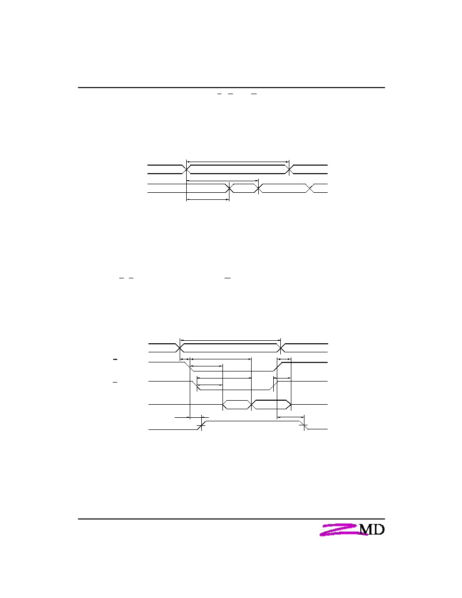
t
PU
t
dis(G)
t
dis(E)
t
cR
Previous
Data Valid
Output Data
Valid
Address Valid
Address Valid
t
su(A )
High-Z
t
en(E)
t
en(G)
t
a(G)
t
a(E)
Read Cycle 1: A
i
-controlled (during Read Cycle : E = G = V
IL
, W = V
IH
)
Read Cycle 2: G-, E-controlled (during Read Cycle: W = V
IH
)
t
a(A)
t
cR
t
v(A)
AAAA
AAAA
AAAA
AAAA
AAA
AAA
AAA
AAA
AAAA
AAAA
AAAA
AAAA
AAAA
AAAA
AAAA
AAAA
AAA
AAA
AAA
AAA
A
i
DQ
i
Output
AAAA
AAAA
AAAA
AAAA
AAAA
AAAA
AAAA
AAAA
AAA
AAA
AAA
AAA
A
i
G
DQ
i
Output
t
PD
A
AA
AAAAAAAAAAAAAAAAAAAAA
A
A
AAAAAAAAAAA
I
CC(OP)
I
CC(SB)
50 %
50 %
Output Data
Valid
E
8
March 8, 1999
U62H256S
AAAA
AAAA
AAAA
AAAA
AAAA
AAAA
AAAA
AAAA
AAAA
AAAA
AAAA
AAAA
A
A
A
A
AAAA
AAAA
AAAA
AAAA
AAAA
AAAA
AAAA
AAAA
AAAA
AAAA
AAAA
AAAA
A
A
A
A
AAAA
AAAA
AAAA
AAAA
AAAA
AAAA
AAAA
AAAA
AAAA
AAAA
AAAA
AAAA
L- to H-level
undefined
H- to L-level
The information describes the type of component and shall not be considered as assured characteristics.Terms of delivery and
rights to change design reserved.
Input Data
Valid
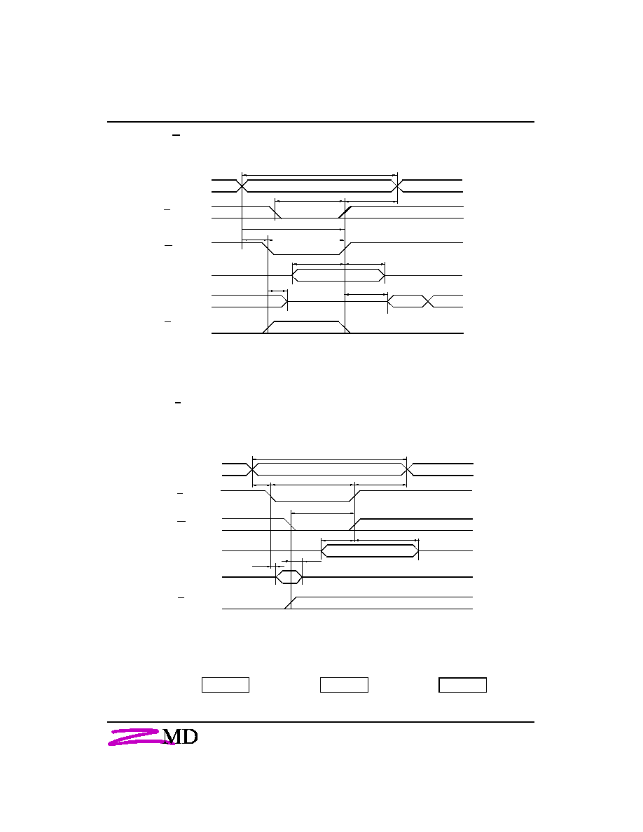
Write Cycle1: W-controlled
Write Cycle 2: E-controlled
t
su(A )
t
h(D)
A
i
E
W
DQ
i
Input
G
DQ
i
Output
t
cW
t
w(E)
t
h(A )
t
su(W)
t
su(D)
t
dis(W)
t
en(E)
High-Z
AAAA
AAAA
AAAA
AAAA
AAAA
AAAA
AAAA
AAAA
AAAA
AAAA
AAAA
AAAA
AAAA
AAAA
AAAA
AAAA
AAA
AAA
AAA
AAA
AAAA
AAAA
AAAA
AAAA
AAAA
AAAA
AAAA
AAAA
AAAA
AAAA
AAAA
AAAA
AAAA
AAAA
AAAA
AAAA
AAAA
AAAA
AAAA
AAAA
AAAA
AAAA
AAAA
AAAA
AAAA
AAAA
AAAA
AAAA
AAAA
AAAA
AAAA
AAAA
t
h(D)
A
i
E
W
DQ
i
Input
G
DQ
i
Output
t
cW
t
su(E)
t
h(A )
t
w(W)
t
su(A )
t
su(D)
t
dis(W)
t
en(W)
Address Valid
Input Data
Valid
High-Z
AAAA
AAAA
AAAA
AAAA
AAAA
AAAA
AAAA
AAAA
AAAA
AAAA
AAAA
AAAA
AAAA
AAAA
AAAA
AAAA
AAAA
AAAA
AAAA
AAAA
AAAA
AAAA
AAAA
AAAA
AAAA
AAAA
AAAA
AAAA
AAAA
AAAA
AAAA
AAAA
AAAA
AAAA
AAAA
AAAA
AAAA
AAAA
AAAA
AAAA
AAAA
AAAA
AAAA
AAAA
AAAA
AAAA
AAAA
AAAA
AAA
AAA
AAA
AAA
AAAA
AAAA
AAAA
AAAA
AAAA
AAAA
AAAA
AAAA
AAA
AAA
AAA
AAA
AAAA
AAAA
AAAA
AAAA
AAAA
AAAA
AAAA
AAAA
AAAA
AAAA
AAAA
AAAA
AAAA
AAAA
AAAA
AAAA
AAAA
AAAA
AAAA
AAAA
AAA
AAA
AAA
AAA
t
su(A -WH)
AAAA
AAAA
AAAA
AAAA
AAAA
AAAA
AAAA
AAAA
AAAA
AAAA
AAAA
AAAA
AAAA
AAAA
AAAA
AAAA
AAAA
AAAA
AAAA
AAAA
AAAA
AAAA
AAAA
AAAA
AAAA
AAAA
AAAA
AAAA
AAAA
AAAA
AAAA
AAAA
AAAA
AAAA
AAAA
AAAA
AAAA
AAAA
AAAA
AAAA
AAAA
AAAA
AAAA
AAAA
AAAA
AAAA
AAAA
AAAA
Address Valid

Zentrum Mikroelektronik Dresden GmbH
Grenzstrasse 28
∑
D-01109 Dresden
∑
P. O. B. 80 01 34
∑
D-01101 Dresden
∑
Germany
Phone:
+49
351
88
22-3
06
∑
Fax:
+49
351
88
22-3
37
∑
Email: sales@zmd.de
∑
http://www.zmd.de
LIFE SUPPORT POLICY
ZMD products are not designed, intended, or authorized for use as components in
systems intended for surgical implant into the body, or other applications intended
to support or sustain life, or for any other application in which the failure of the ZMD
product could create a situation where personal injury or death may occur.
Components used in life-support devices or systems must be expressly authorized
by ZMD for such purpose.
LIMITED WARRANTY
The information in this document has been carefully checked and is believed to be
reliable. However Zentrum Mikroelektronik Dresden GmbH (ZMD) makes no
guarantee or warranty concerning the accuracy of said information and shall not be
responsible for any loss or damage of whatever nature resulting from the use of, or
reliance upon it. The information in this document describes the type of component
and shall not be considered as assured characteristics.
ZMD does not guarantee that the use of any information contained herein will not
infringe upon the patent, trademark, copyright, mask work right or other rights of
third parties, and no patent or licence is implied hereby. This document does not in
any way extent ZMD's warranty on any product beyond that set forth in its standard
terms and conditions of sale.
ZMD reserves terms of delivery and reserves the right to make changes in the
products or specifications, or both, presented in this publication at any time and
without notice.