
U62H824
November 26, 2002
1
!
196 608 bit static CMOS RAM
!
35 ns Access Time
!
Fully static Read and Write
operations
!
Equal address and chip
enable access times
!
Single bit on-chip address
multiplexer
!
Active high and active low
chip enable inputs
!
Output enable controlled three-
state outputs
!
TTL/CMOS-compatible
!
Low power standby mode
!
Power supply voltage 5 V
!
Operating temperature range
0 to 70
∞C
-40 to 85
∞C
-40 to 125 ∞C
!
QS 9000 Quality Standard
!
ESD protection > 2000 V
(MIL STD 883C M3015.7)
!
Latch-up immunity > 100 mA
!
Package: PLCC52
The U62H824 is a static RAM
manufactured using a CMOS pro-
cess technology. The device inte-
grates an 8K x 24 SRAM core with
multiple chip enable inputs, output
enable, and an externally control-
led single address pin multiplexer.
These functions allow for direct
connection to the Motorola
DSP56k Digital Signal Processor
Family and provide a very efficient
means for implementation of a
reduced parts count system requi-
ring no additional interface logic.
The avialability of multiple chip
enable (E1 and E2) and output
enable (G) inputs provides for
greater system flexibility when mul-
tiple devices are used. With either
chip enable unasserted, the device
will enter standby mode, useful in
low-power applications. A single
on-chip multiplexer selects A12 or
X/Y as the highest order address
input depending upon the state of
the V/S control input. This feature
allows one physical static RAM
component to efficiently store pro-
gram and vector or scalar ope-
rands by dynamically re-
partitioning the RAM array.
Typical applications will logically
map vector operands into upper
memory with scalar operands
being stored in lower memory.
An application example is at the
end of this document for additional
information.
Multiple power and ground pins
have been utilized to minimize
effectes induced by output noice.
Fast 8K x 24 SRAM
Pin Configuration
DQ23
DQ22
VSS
DQ20
DQ21
DQ19
DQ18
DQ17
DQ14
DQ16
DQ15
VSS
DQ13
Signal Name
Signal Description
A0 - A11
Address Inputs
A12, X/Y
Multiplexed Address
V/S
Address Multiplexer Control
DQ0 - DQ23
Data Input / Output
E1, E2
Chip Enable
G
Output Enable
W
Write Enable
VCC
Power Supply Voltage
VSS
Ground
NC
Not Connected
Pin Description
For proper operation of the device, all V
SS
pins must be connected to ground.
1
2
3
4
5
6
7
8
10
9
11
12
13
14
15
16
17
18
19
20
21
23 24 25 26 27 28 29 30 31 32 33
22
52 51 50 49 48 47
A10
A1
1
X/
Y
V/
S
A12
NC
VCC
A0
A4
A1
A2
A3
A5
DQ0
DQ1
VSS
DQ3
DQ2
DQ4
DQ5
DQ6
DQ9
DQ7
DQ8
VSS
DQ10
DQ1
1
A9
A7
A6
A8
G
VCC
VSS
NC
E1
E2
W
DQ
1
2
46
44
45
43
42
41
40
39
38
37
36
35
34
Features
Description
U62H824
November 26, 2002
2
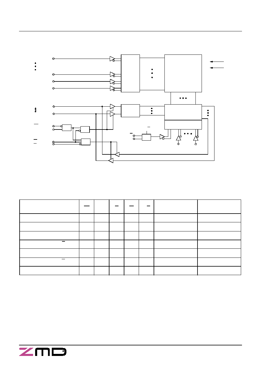
Block Diagram
DQ23
DQ0
G
W
E2
E1
&
&
&
1
0
(LSB)
(MSB)
Input Data
Control
2 to 1 MUX
V/S
Q
Row
Decoder
Memory Cell
Array
256 Rows x
768 Columns
V
CC
V
SS
Column I/O
Column Decoder
A12i
X/Y
A12
A0
A5
A10
A11
A6
A9
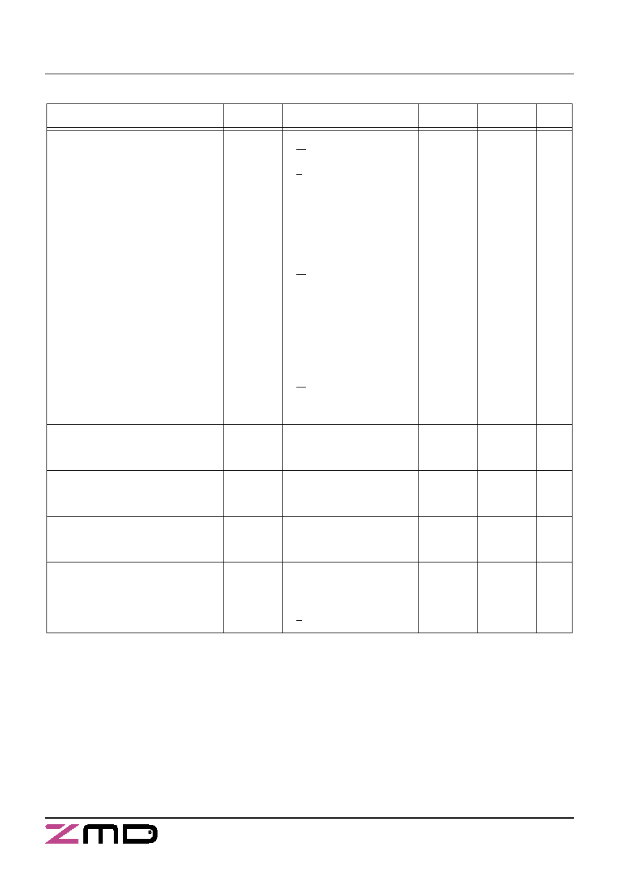
* H or L
Mode
E1
E2
G
W
V/S
Supply
Current
I/O
Status
Not Selected
H
*
*
*
*
I
CC(SB)
High - Z
Not Selected
*
L
*
*
*
I
CC(SB)
High - Z
Output Disable
L
H
H
H
*
I
CC(OP)
High - Z
Read Using X/Y
L
H
L
H
H
I
CC(OP)
Data Out
Read Using A12
L
H
L
H
L
I
CC(OP)
Data Out
Write Using X/Y
L
H
*
L
H
I
CC(OP)
Data In
Write Using A12
L
H
*
L
L
I
CC(OP)
Data In
Truth Table

U62H824
November 26, 2002
3
Characteristics
All voltages are referenced to V
SS
= 0 V (ground).
All characteristics are valid in the power supply voltage range and in the operating temperature range specified.
Dynamic measurements are based on a rise and fall time of
5 ns, measured between 10 % and 90 % of V
I
, as well as
input levels of V
IL
= 0 V and V
IH
= 3 V. The timing reference level of all input and output signals is 1.5 V,
with the exception of the t
dis
-times and t
en
-times, in which cases transition is measured
± 200 mV from steady-state voltage.
d
-2 V at Pulse Width 10 ns
Recommended
Operating Conditions
Symbol
Conditions
Min.
Max.
Unit
Power Supply Voltage
V
CC
4.5
5.5
V
Input Low Voltage
d
V
IL
-0.3
0.8
V
Input High Voltage
V
IH
2.2
V
CC
+ 0.3
V
a
Stresses greater than those listed under ,,Absolute Maximum Ratings" may cause permanent damage to the device. This is a stress rating
only, and functional operation of the device at condition above those indicated in the operational sections of this specification is not implied.
Exposure to absolute maximum rating conditions for extended periods may affect reliability
b
Maximum voltage is 7 V
c
Not more than 1 output should be shorted at the same time. Duration of the short circuit should not exceed 30 s.
Absolute Maximum Ratings
a
Symbol
Min.
Max.
Unit
Power Supply Voltage
V
CC
-0.5
7
V
Input Voltage
V
I
-0.5
V
CC
+ 0.5
b
V
Output Voltage
V
O
-0.5
V
CC
+ 0.5
b
V
Power Dissipation
P
D
-
1.75
W
Operating Temperature
C-Type
K-Type
A-Type
T
a
0
-40
-40
70
85
125
∞C
∞C
∞C
Storage Temperature
T
stg
-65
150
∞C
Output Short-Circuit Current
at V
CC
= 5 V and V
O
= 0 V
c
|I
OS
|
20
mA
U62H824
November 26, 2002
4
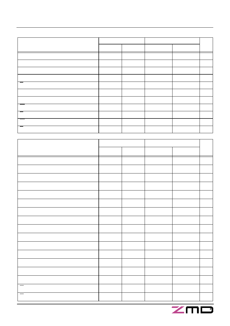
Electrical Characteristics
Symbol
Conditions
Min.
Max.
Unit
Supply Current - Operating Mode
Supply Current - Standby Mode
(CMOS level)
Supply Current - Standby Mode
(TTL level)
I
CC(OP)
I
CC(SB)
I
CC(SB)1
V
CC
V
E1
V
E2
V
G
other inputs
I
out
t
cW
C/K-Type
A-Type
V
CC
V
E1
V
E2
all inputs
C-Type
K-Type
A-Type
V
CC
V
E1
V
E2
all inputs
= 5.5 V
= 0.8 V
= 2.2 V
= 2.2 V
= V
IL
or V
IH
= 0 mA
= 35 ns
= 5.5 V
= V
CC
- 0.2 V
= 0.2 V
V
CC
- 0.2 V
or
0.2 V
= 5.5 V
= 2.2 V
= 0.8 V
= V
IH
or V
IL
170
180
6
8
10
15
mA
mA
mA
mA
mA
mA
Output High Voltage
Output Low Voltage
V
OH
V
OL
V
CC
I
OH
I
OL
= 4.5 V
= -4.0 mA
= 8.0 mA
2.4
0.4
V
V
Input High Leakage Current
Input Low Leakage Current
I
IH
I
IL
V
CC
V
IH
V
IL
= 5.5 V
= 5.5 V
= 0 V
-2
2
µA
µA
Output High Current
Output Low Current
I
OH
I
OL
V
CC
V
OH
V
OL
= 4.5
V
= 2.4 V
= 0.4 V
8
-4
mA
mA
Output Leakage Current
High at Three-State Outputs
Low at Three-State Outputs
I
OHZ
I
OLZ
V
CC
V
OH
V
OL
V
G
= 5.5
V
= 5.5 V
= 0 V
= V
IH
-2
2
µA
µA
U62H824
November 26, 2002
5
Switching Characteristics
Read Cycle
Symbol
35
Unit
Alt.
IEC
Min.
Max.
Read Cycle Time
t
RC
t
cR
35
ns
Address Access Time to Data Valid
t
AA
t
a(A)
35
ns
MUX Control to Data Valid
t
a(VS)
35
Chip Enable Access Time to Data Valid
t
ACE
t
a(E)
35
ns
G LOW to Data Valid
t
OE
t
a(G)
15
ns
Output Hold Time from Address Change
t
OH
t
v(A)
5
ns
Output Hold Time from MUX Control Change
t
v(VS)
5
ns
E1 LOW or E2 HIGH to Output in Low-Z
t
LZCE
t
en(E)
0
ns
G LOW to Output in Low-Z
t
LZOE
t
en(G)
0
ns
E1 HIGH or E2 LOW to Output in High-Z
t
HZCE
t
dis(E)
15
ns
G HIGH to Output in High-Z
t
HZOE
t
dis(G)
15
ns
Switching Characteristics
Write Cycle
Symbol
35
Unit
Alt.
IEC
Min.
Max.
Write Cycle Time
t
WC
t
cW
35
ns
Write Pulse Width
t
WP
t
w(W)
20
ns
Write Pulse Width Setup Time
t
WP
t
su(W)
20
ns
Address Setup Time
t
AS
t
su(A)
0
ns
MUX Control Setup Time
t
su(VS)
0
ns
Address Valid to End of Write
t
AW
t
su(A-WH)
30
ns
MUX Control Valid to End of Write
t
su(VS-WH)
30
ns
Adress Valid to End of Write
t
su(A-E)
30
ns
MUX Control Valid to End of Write
t
su(VS-E)
30
ns
Chip Enable Setup Time
t
CW
t
su(E)
20
ns
Pulse Width Chip Enable
t
CW
t
w(E)
20
ns
Data Setup Time
t
DS
t
su(D)
15
ns
Data Hold Time
t
DH
t
h(D)
0
ns
Address Hold from End of Write
t
AH
t
h(A)
0
ns
MUX Control from End of Write
t
h(VS)
0
ns
W HIGH to Output in Low-Z
t
LZWE
t
en(W)
5
ns
W LOW to Output in High-Z
t
HZWE
t
dis(W)
15
ns