1
August 11, 2003
U630H16
!
High-performance CMOS nonvo-
latile static RAM 2048 x 8 bits
!
25, 35 and 45 ns Access Times
!
12, 20 and 25 ns Output Enable
Access Times
!
Hardware STORE Initiation
(STORE Cycle Time < 10 ms)
!
Automatic STORE Timing
!
10
5
STORE cycles to EEPROM
!
10 years data retention in
EEPROM
!
Automatic RECALL on Power Up
!
Hardware RECALL Initiation
(RECALL Cycle Time < 20
µs)
!
Unlimited RECALL cycles from
EEPROM
!
Unlimited Read and Write to
SRAM
!
Single 5 V
± 10 % Operation
!
Operating temperature ranges:
0 to 70
∞C
-40 to 85
∞C
-40 to 125 ∞C (only 35 ns)
!
QS 9000 Quality Standard
!
ESD characterization according
MIL STD 883C M3015.7-HBM
(classification see IC Code Num-
bers)
!
Packages: SOP28 (300 mil),
PDIP28 (300/600 mil,
only C/K-Type)
The U630H16 has two separate
modes of operation: SRAM mode
and nonvolatile mode, determined
by the state of the NE pin.
In SRAM mode, the memory ope-
rates as an ordinary static RAM. In
nonvolatile operation, data is trans-
ferred in parallel from SRAM to
EEPROM or from EEPROM to
SRAM. In this mode SRAM
functions are disabled.
The U630H16 is a fast static RAM
(25, 35, 45 ns), with a nonvolatile
electrically erasable PROM
(EEPROM) element incorporated
in each static memory cell. The
SRAM can be read and written an
unlimited number of times, while
independent nonvolatile data resi-
des in EEPROM. Data transfers
from the SRAM to the EEPROM
(the STORE operation), or from the
EEPROM to the SRAM (the
RECALL operation) are initiated
through the state of the NE pin.
The U630H16 combines the high
performance and ease of use of a
fast SRAM with nonvolatile data
integrity.
Once a STORE cycle is initiated,
further input or output are disabled
until the cycle is completed.
Internally, RECALL is a two step
procedure. First, the SRAM data is
cleared and second, the nonvola-
tile information is transferred into
the SRAM cells.
The RECALL operation in no way
alters the data in the EEPROM
cells. The nonvolatile data can be
recalled an unlimited number of
times.
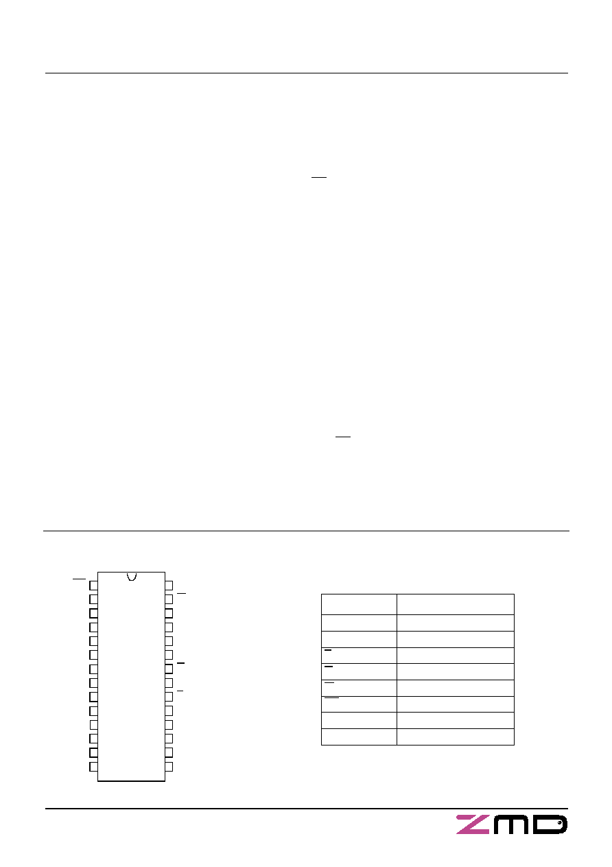
HardStore 2K x 8 nvSRAM
Pin Configuration
Pin Description
Top View
1
NE
VCC
28
2
n.c.
W
27
4
A6
A8
25
5
A5
A9
24
3
A7
n.c.
26
6
A4
n.c.
23
7
A3
G
22
8
A2
A10
21
12
DQ1
DQ5
17
9
A1
E
20
10
A0
DQ7
19
11
DQ0
DQ6
18
13
DQ2
DQ4
16
14
VSS
DQ3
15
PDIP
SOP
Signal Name
Signal Description
A0 - A10
Address Inputs
DQ0 - DQ7
Data In/Out
E
Chip Enable
G
Output Enable
W
Write Enable
NE
Nonvolatile Enable
VCC
Power Supply Voltage
VSS
Ground
Features
Description
2
August 11, 2003
U630H16
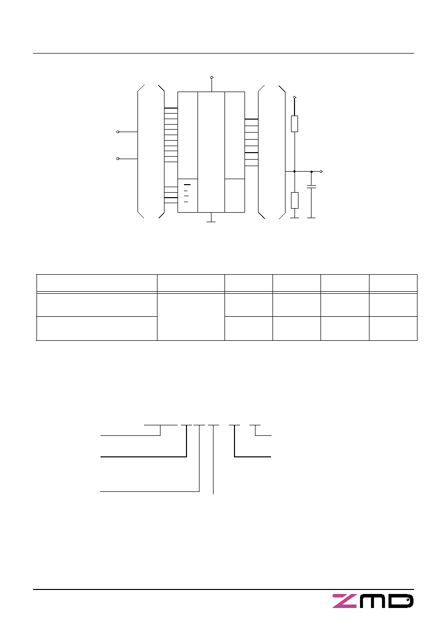
Block Diagram
Operating Mode
E
NE
W
G
DQ0 - DQ7
Standby/not selected
H
*
*
*
High-Z
Internal Read
L
H
H
H
High-Z
Read
L
H
H
L
Data Outputs Low-Z
Write
L
H
L
*
Data Inputs High-Z
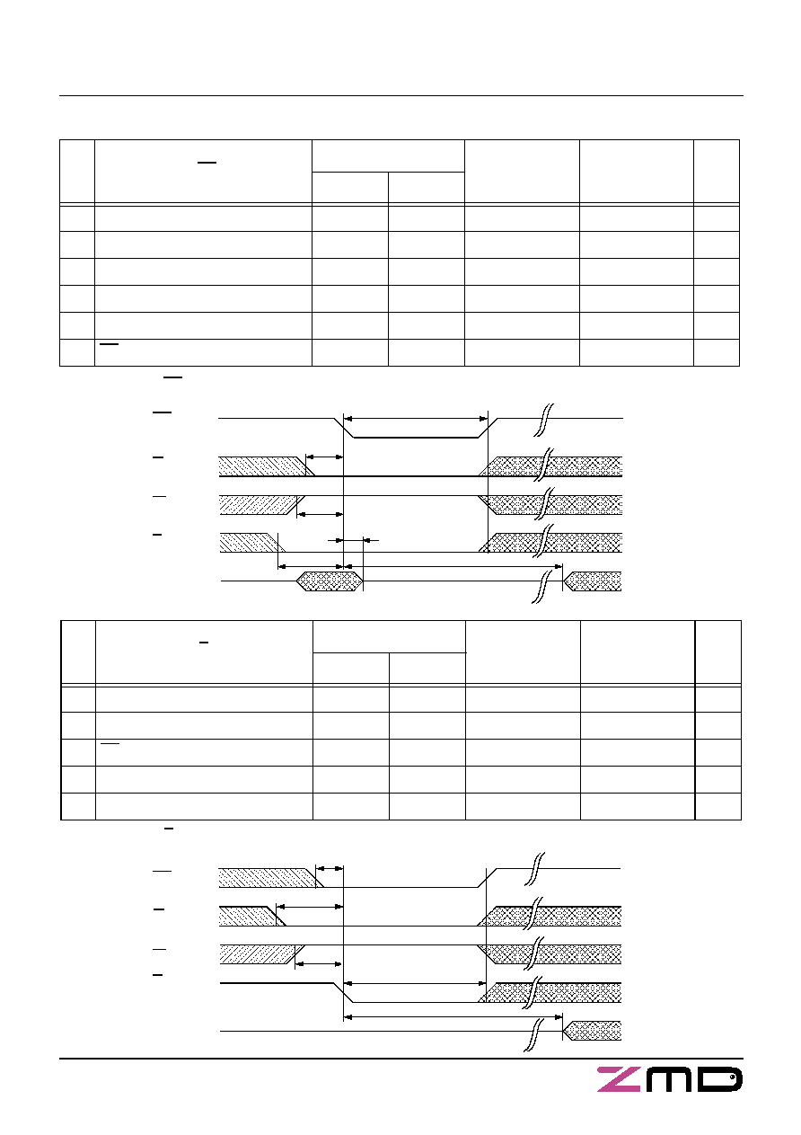
Truth Table for SRAM Operations
a: Stresses greater than those listed under ,,Absolute Maximum Ratings" may cause permanent damage to the device. This is a stress
rating only, and functional operation of the device at condition above those indicated in the operational sections of this specification is
not implied. Exposure to absolute maximum rating conditions for extended periods may affect reliability.
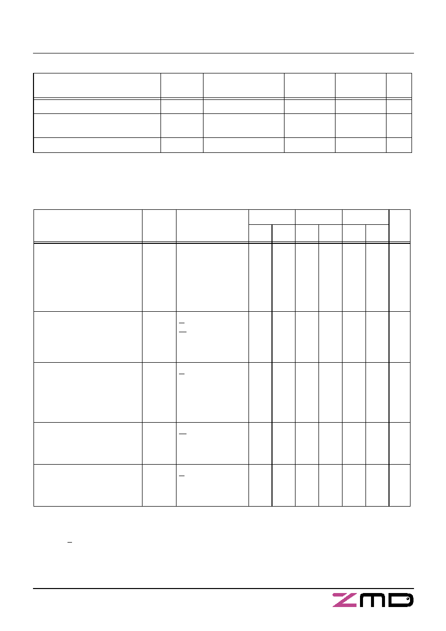
Absolute Maximum Ratings
a
Symbol
Min.
Max.
Unit
Power Supply Voltage
V
CC
-0.5
7
V
Input Voltage
V
I
-0.3
V
CC
+0.5
V
Output Voltage
V
O
-0.3
V
CC
+0.5
V
Power Dissipation
P
D
1
W
Operating Temperature
C-Type
K-Type
A-Type
T
a
0
-40
-40
70
85
85
∞C
∞C
∞C
Storage Temperature
T
stg
-65
150
∞C
Characteristics
All voltages are referenced to V
SS
= 0 V (ground).
All characteristics are valid in the power supply voltage range and in the operating temperature range specified.
Dynamic measurements are based on a rise and fall time of
5 ns, measured between 10 % and 90 % of V
I
, as well as
input levels of V
IL
= 0 V and V
IH
= 3 V. The timing reference level of all input and output signals is 1.5 V,
with the exception of the t
dis
-times and t
en
-times, in which cases transition is measured
± 200 mV from steady-state voltage.
*
H or L
EEPROM Array
32 x (64 x 8)
STORE
RECALL
SRAM
Array
32 Rows x
64 x 8 Columns
A5
A6
A7
A8
A9
Store/
Recall
Control
Ro
w De
c
o
d
e
r
V
CC
V
SS
V
CC
G
NE
E
W
DQ0
DQ1
DQ2
DQ3
DQ4
DQ5
DQ6
DQ7
Column I/O
Column Decoder
A0 A1
A2
A3
A4A10
I
n
p
u
t Bu
ffe
r
s
3
August 11, 2003
U630H16
b: I
CC1
and I
CC3
are dependent on output loading and cycle rate. The specified values are obtained with outputs unloaded.
The current I
CC1
is measured for WRITE/READ - ratio of 1/2.
c: I
CC2
is the average current required for the duration of the STORE cycle (STORE Cycle Time).
d: Bringing E
V
IH
will not produce standby current levels until any nonvolatile cycle in progress has timed out. See MODE SELECTION
table. The current I
CC(SB)1
is measured for WRITE/READ - ratio of 1/2.
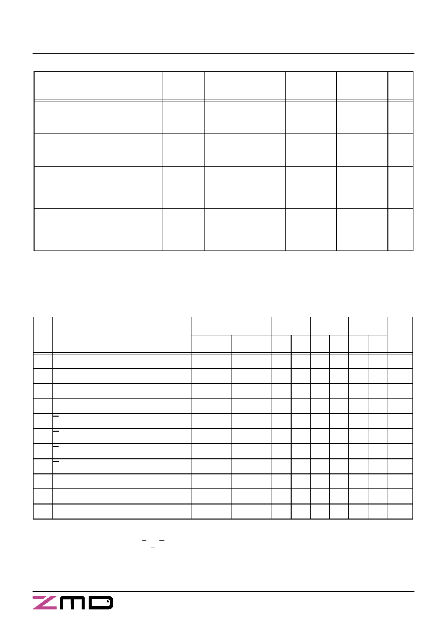
DC Characteristics
Symbol
Conditions
C-Type
K-Type
A-Type
Unit
Min. Max. Min. Max. Min. Max.
Operating Supply Current
b
I
CC1
V
CC
V
IL
V
IH
t
c
t
c
t
c
= 5.5 V
= 0.8 V
= 2.2 V
= 25 ns
= 35 ns
= 45 ns
90
80
75
95
85
80
-
85
-
mA
mA
mA
Average Supply Current during
STORE
c
I
CC2
V
CC
E
W
V
IL
V
IH
= 5.5 V
V
CC
-0.2 V
V
CC
-0.2 V
0.2 V
V
CC
-0.2 V
6
7
7
mA
Standby Supply Current
d
(Cycling TTL Input Levels)
I
CC(SB)1
V
CC
E
t
c
t
c
t
c
= 5.5 V
V
IH
= 25 ns
= 35 ns
= 45 ns
30
23
20
34
27
23
-
27
-
mA
mA
mA
Average Supply Current
at t
cR
= 200 ns
b
(Cycling CMOS Input Levels)
I
CC3
V
C
C
W
V
IL
V
IH
= 5.5 V
V
CC
-0.2 V
0.2 V
V
CC
-0.2 V
15
15
15
mA
Standby Supply Current
d
(Stable CMOS Input Levels)
I
CC(SB)
V
CC
E
V
IL
V
IH
= 5.5 V
V
CC
-0.2 V
0.2 V
V
CC
-0.2 V
1
1
2
mA
Recommended
Operating Conditions
Symbol
Conditions
Min.
Max.
Unit
Power Supply Voltage
V
CC
4.5
5.5
V
Input Low Voltage
V
IL
-2 V at Pulse Width
10 ns permitted
-0.3
0.8
V
Input High Voltage
V
IH
2.2
V
CC
+0.3
V
4
August 11, 2003
U630H16
DC Characteristics
Symbol
Conditions
Min.
Max.
Unit
Output High Voltage
Output Low Voltage
V
OH
V
OL
V
CC
I
OH
I
OL
= 4.5 V
=-4 mA
= 8 mA
2.4
0.4
V
V
Output High Current
Output Low Current
I
OH
I
OL
V
CC
V
OH
V
OL
= 4.5 V
= 2.4 V
= 0.4 V
8
-4
mA
mA
Input Leakage Current
High
Low
I
IH
I
IL
V
CC
V
IH
V
IL
= 5.5 V
= 5.5 V
= 0 V
-1
1
µA
µA
Output Leakage Current
High at Three-State- Output
Low at Three-State- Output
I
OHZ
I
OLZ
V
CC
V
OH
V
OL
= 5.5 V
= 5.5 V
= 0 V
-1
1
µA
µA
SRAM Memory Operations
No.
Switching Characteristics
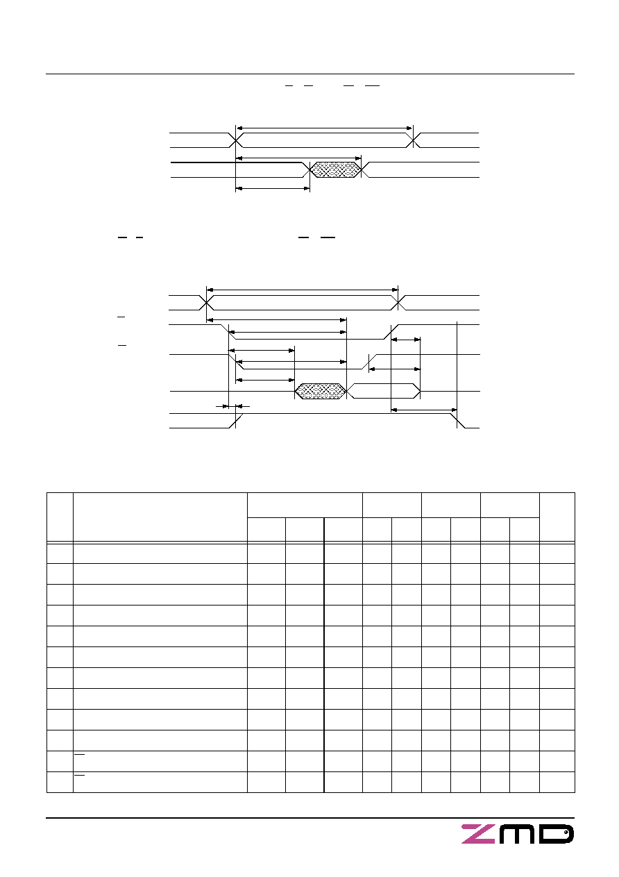
Read Cycle
Symbol
25
35
45
Unit
Alt.
IEC
Min. Max. Min. Max. Min. Max.
1
Read Cycle Time
f
t
AVAV
t
cR
25
35
45
ns
2
Address Access Time to Data Valid
g
t
AVQV
t
a(A)
25
35
45
ns
3
Chip Enable Access Time to Data Valid
t
ELQV
t
a(E)
25
35
45
ns
4
Output Enable Access Time to Data Valid
t
GLQV
t
a(G)
12
20
25
ns
5
E HIGH to Output in High-Z
h
t
EHQZ
t
dis(E)
13
17
20
ns
6
G HIGH to Output in High-Z
h
t
GHQZ
t
dis(G)
13
17
20
ns
7
E LOW to Output in Low-Z
t
ELQX
t
en(E)
5
5
5
ns
8
G LOW to Output in Low-Z
t
GLQX
t
en(G)
0
0
0
ns
9
Output Hold Time after Addr. Change
g
t
AXQX
t
v(A)
3
3
3
ns
10 Chip Enable to Power Active
e
t
ELICCH
t
PU
0
0
0
ns
11 Chip Disable to Power Standby
d, e
t
EHICCL
t
PD
25
35
45
ns
e: Parameter guaranteed but not tested.
f:
Device is continuously selected with E and G both LOW.
g: Address valid prior to or coincident with E transition LOW.
h: Measured
± 200 mV from steady state output voltage.
5
August 11, 2003
U630H16
Read Cycle 1: Ai-controlled (during Read cycle: E = G = V
IL
, W = NE = V
IH
)
f
t
a(A)
Output Data Valid
t
cR
Address Valid
t
v(A)
Ai
DQi
Output
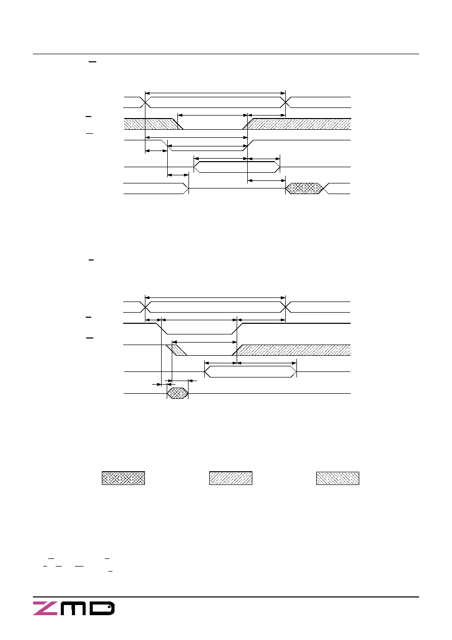
Read Cycle 2: G-, E-controlled (during Read cycle: W = NE = V
IH
)
g
Ai
E
G
DQi
Output
t
dis(E)
t
cR
t
a(E)
t
en(E)
t
en(G)
t
a(G)
t
dis(G)
Address Valid
High Impedance
I
CC
ACTIVE
STANDBY
t
PD
t
PU
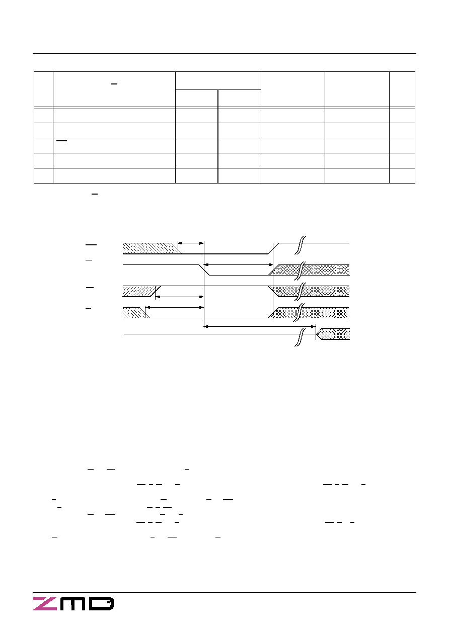
No. Switching Characteristics
Write Cycle
Symbol
25
35
45
Unit
Alt. #1 Alt. #2
IEC
Min. Max. Min. Max. Min. Max.
12 Write Cycle Time
t
AVAV
t
AVAV
t
cW
25
35
45
ns
13 Write Pulse Width
t
WLWH
t
w(W)
20
30
35
ns
14 Write Pulse Width Setup Time
t
WLEH
t
su(W)
20
30
35
ns
15 Address Setup Time
t
AVWL
t
AVEL
t
su(A)
0
0
0
ns
16 Address Valid to End of Write
t
AVWH
t
AVEH
t
su(A-WH)
20
30
35
ns
17 Chip Enable Setup Time
t
ELWH
t
su(E)
20
30
35
ns
18 Chip Enable to End of Write
t
ELE
H
t
w(E)
20
30
35
ns
19 Data Setup Time to End of Write
t
DVWH
t
DVEH
t
su(D)
12
18
20
ns
20 Data Hold Time after End of Write
t
WHDX
t
EHDX
t
h(D)
0
0
0
ns
21 Address Hold after End of Write
t
WHAX
t
EHAX
t
h(A)
0
0
0
ns
22 W LOW to Output in High-Z
h, i
t
WLQZ
t
dis(W)
10
13
15
ns
23 W HIGH to Output in Low-Z
t
WHQX
t
en(W)
5
5
5
ns
(1)
(2)
(9)
(1)
(3)
(4)
(5)
(7)
(6)
(8)
(10)
(11)
t
a(A)
(2)
Previous Data Valid
Output Data Valid
6
August 11, 2003
U630H16
t
h(D)
Write Cycle #1: W-controlled
j
Ai
E
W
DQi
Input
DQi
Output
t
cW
t
su(E)
t
h(A)
t
w(W)
t
su(A)
t
su(D)
t
dis(W)
t
en(W)
Input Data Valid
High Impedance
t
su(A)
Write Cycle #2: E-controlled
j
t
h(D)
Ai
E
W
DQi
Input
DQi
Output
t
cW
t
w(E)
t
h(A)
t
su(D)
t
dis(W)
t
en(E)
Input Data Valid
High Impedance
t
su(W)
L- to H-level
undefined
H- to L-level
i:
If W is LOW and when E goes LOW, the outputs remain in the high impedance state.
j:
E or W and NE must be > V
IH
during address transitions.
t
su(A-WH)
Previous Data
(12)
(17)
(16)
(13)
(19)
(20)
(23)
(22)
(15)
(21)
(12)
(15)
(18)
(21)
(14)
(20)
(19)
(22)
(7)
Address Valid
Address Valid
7
August 11, 2003
U630H16
Nonvolatile Memory Operations
No.
STORE Cycle Inhibit and
Automatic Power Up RECALL
Symbol
Min.
Max.
Unit
Alt.
IEC
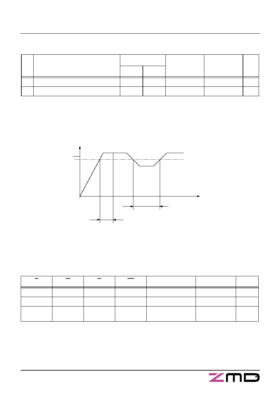
24
Power Up RECALL Duration
k, e
t
RESTORE
650
µs
Low Voltage Trigger Level
V
SWITCH
4.0
4.5
V
k: t
RESTORE
starts from the time V
CC
rises above V
SWITCH
.
STORE Cycle Inhibit and Automatic Power Up RECALL
V
CC
5.0 V
STORE inhibit
Power Up
V
SWITCH
t
RESTORE
RECALL
(24)
t
Mode Selection
E
W
G
NE
Mode
Power
Notes
L
H
L
L
Nonvolatile RECALL
Active
l
L
L
H
L
Nonvolatile STORE
I
CC2
L
L
L
H
L
H
L
*
No operation
Active
*
H or L
l:
An automatic RECALL also takes place at power up, starting when V
CC
exceeds V
SWITCH
and takes t
RESTORE
. V
CC
must not drop below
V
SWITCH
once it has been exceeded for the RECALL to function properly.
8
August 11, 2003
U630H16
STORE Cycles
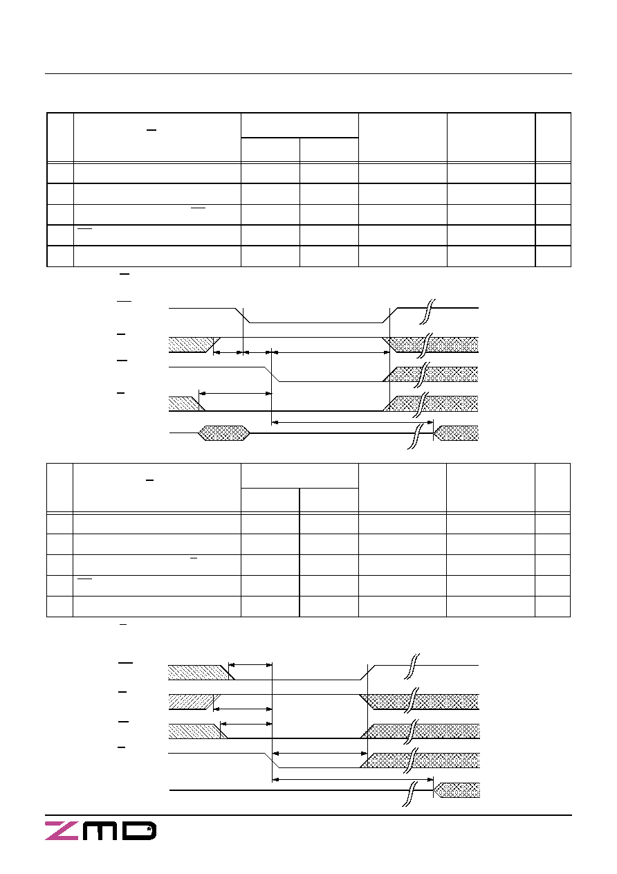
No. STORE Cycle W-controlled
Symbol
Min.
Max.
Unit
Alt.
IEC
25
STORE Cycle Time
m
t
WLQX
t
d(W)S
10
ms
26
STORE Initiation Cycle Time
n
t
WLNH
t
w(W)S
25
ns
27
Output Disable Setup to NE Fall
t
GHNL
t
su(G)S
5
ns
28
NE Setup
t
NLWL
t
su(N)S
5
ns
29
Chip Enable Setup
t
ELWL
t
su(E)S
5
ns
STORE Cycle: W-controlled
o
t
su(G)S
t
su(N)S
t
w(W)S
t
su(E)S
t
d(W)S
High Impedance
(25)
(29)
(28)
(27)
(26)
NE
G
W
E
DQi
Output
STORE Cycle: E-controlled
o
No. STORE Cycle E-controlled
Symbol
Min.
Max.
Unit
Alt.
IEC
30
STORE Cycle Time
t
ELQXS
t
d(E)S
10
ms
31
STORE Initiation Cycle Time
t
ELNHS
t
w(E)S
25
ns
32
Output Disable Setup to E Fall
t
GHEL
t
su(G)S
5
ns
33
NE Setup
t
NLEL
t
su(N)S
5
ns
34
Write Enable Setup
t
WLEL
t
su(W)S
5
ns
t
su(N)S
t
su(G)S
t
su(W)S
t
d(E)S
High Impedance
(30)
(31)
(33)
(32)
(34)
t
w(E)S
NE
G
W
E
DQi
Output
9
August 11, 2003
U630H16
RECALL Cycles
No. RECALL Cycle NE-controlled
Symbol
Min.
Max.
Unit
Alt.
IEC
35
RECALL Cycle Time
p
t
NLQX
t
d(N)R
20
µs
36
RECALL Initiation Cycle Time
q
t
NLNH
t
w(N)R
25
ns
37
Output Enable Setup
t
GLNL
t
su(G)R
5
ns
38
Write Enable Setup
t
WHNL
t
su(W)R
5
ns
39
Chip Enable Setup
t
ELNL
t
su(E)R
5
ns
40
NE Fall to Output Inactive
t
NLQZ
t
dis(N)R
25
ns
RECALL Cycle: NE-controlled
o
t
w(N)R
(36)
NE
G
W
E
DQi
Output
t
su(G)R
t
su(W)R
t
su(E)R
t
d(N)R
t
dis(N)R
(37)
(38)
(40)
(35)
(39)
High Impedance
No. RECALL Cycle E-controlled
Symbol
Min.
Max.
Unit
Alt.
IEC
41
RECALL Cycle Time
t
ELQXR
t
d(E)R
20
µs
42
RECALL Initiation Cycle Time
t
ELNHR
t
w(E)R
25
ns
43
NE Setup
t
NLEL
t
su(N)R
5
ns
44
Output Enable Setup
t
GLEL
t
su(G)R
5
ns
45
Write Enable Setup
t
WHEL
t
su(W)R
5
ns
RECALL Cycle: E-controlled
o
NE
G
W
E
DQi
Output
t
su(N)R
t
su(G)R
t
su(W)R
t
w(E)R
t
d(E)R
High Impedance
(41)
(42)
(43)
(45)
(44)
10
August 11, 2003
U630H16
No. RECALL Cycle G-controlled
Symbol
Min.
Max.
Unit
Alt.
IEC
46
RECALL Cycle Time
t
GLQXR
t
d(G)R
20
µs
47
RECALL Initiation Cycle Time
t
GLNH
t
w(G)R
25
ns
48
NE Setup
t
NLGL
t
su(N)R
5
ns
49
Write Enable Setup
t
WHGL
t
su(W)R
5
ns
50
Chip Enable Setup
t
ELGL
t
su(E)R
5
ns
RECALL Cycle: G-controlled
o, r
NE
G
W
E
DQi
Output
t
su(N)R
t
su(W)R
t
su(E)R
t
w(G)R
t
d(G)R
High Impedance
(48)
(47)
(49)
(50)
(46)
m: Measured with W and NE both returned HIGH, and G returned LOW. Note that STORE cycles are inhibited/aborted by V
CC
< V
SWITCH
(STORE inhibit).
n: Once t
w(W)S
has been satisfied by NE, G, W and E, the STORE cycle is completed automatically. Any of NE, G, W and E may be used to
terminate the STORE initiation cycle.
o: If E is LOW for any period of time in which W is HIGH while G and NE are LOW, than a RECALL cycle may be initiated.
For E-controlled STORE during t
w(E)S
W, G, NE have to be static.
p: Measured with W and NE both HIGH, and G and E LOW.
q: Once t
w(N)R
has been satisfied by NE, G, W and E, the RECALL cycle is completed automatically. Any of NE, G or E may be used to
terminate the RECALL initiation cycle.
r:
If W is LOW at any point in which both E and NE are LOW and G is HIGH, than a STORE cycle will be initiated instead of a RECALL.
11
August 11, 2003
U630H16
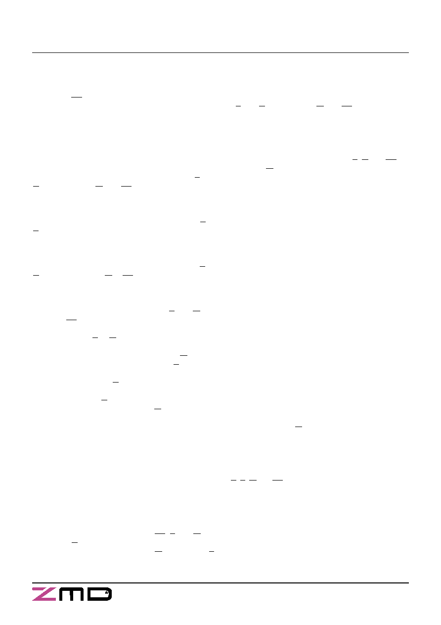
Test Configuration for Functional Check
s: In measurement of t
dis
-times and t
en
-times the capacitance is 5 pF.
t:
Between V
CC
and V
SS
must be connected a high frequency bypass capacitor 0.1
µF to avoid disturbances.
Capacitance
e
Conditions
Symbol
Min.
Max.
Unit
Input Capacitance
V
CC
V
I
f
T
a
= 5.0 V
= V
SS
= 1 MHz
= 25
∞C
C
I
8
pF
Output Capacitance
C
O
7
pF
All pins not under test must be connected with ground by capacitors.
IC Code Numbers
V
IH
V
IL
V
SS
V
CC
t
255
30 pF
s
V
O
S
i
m
u
lt
an
eo
us
m
e
as
ur
e
-
m
ent
of
al
l
8
out
p
u
t
pi
ns
In
p
u
t l
e
v
e
l
a
c
c
o
r
d
in
g
to
th
e
r
e
l
e
v
a
nt
t
e
s
t
me
as
u
r
em
en
t
DQ0
DQ1
DQ2
DQ3
DQ4
DQ5
DQ6
DQ7
A0
A1
A2
A3
A4
A5
A6
A7
A8
A9
A10
E
W
G
5 V
NE
480
The date of manufacture is given by the last 4 digits of the mark, the first 2 digits indicating the year, and the last 2
digits the calendar week.
S
U630H16
25
C
Type
Operating Temperature Range
C =
0 to 70 ∞C
K = -40 to 85 ∞C
A = -40 to 125 ∞C (only 35 ns and SOP28 package)
Access Time
25 = 25 ns
35 = 35 ns (C/K-Type on special request)
45 = 45 ns (on special request)
Package
D = PDIP28 (300 mil)
D1 = PDIP28 (600 mil)
S = SOP28 (300 mil)
Internal Code
B
ESD Class
blank > 2000 V
B > 1000 V
Example
12
August 11, 2003
U630H16
Device Operation
The U630H16 has two separate modes of operation:
SRAM mode and nonvolatile mode, determined by the
state of the NE pin. In SRAM mode, the memory opera-
tes as a standard fast static RAM. In nonvolatile mode,
data is transferred from SRAM to EEPROM (the
STORE operation) or from EEPROM to SRAM (the
RECALL operation). In this mode SRAM functions are
disabled.
SRAM READ
The U630H16 performs a READ cycle whenever E and
G are LOW while W and NE are HIGH. The address
specified on pins A0 - A10 determines which of the
2048 data bytes will be accessed. When the READ is
initiated by an address transition, the outputs will be
valid after a delay of t
cR
. If the READ is initiated by E or
G, the outputs will be valid at t
a(E)
or at t
a(G)
, whichever
is later. The data outputs will repeatedly respond to
address changes within the t
cR
access time without the
need for transition on any control input pins, and will
remain valid until another address change or until E or
G is brought HIGH or W or NE is brought LOW.
SRAM WRITE
A WRITE cycle is performed whenever E and W are
LOW and NE is HIGH. The address inputs must be sta-
ble prior to entering the WRITE cycle and must remain
stable until either E or W goes HIGH at the end of the
cycle. The data on pins DQ0 - 7 will be written into the
memory if it is valid t
su(D
)
before the end of a W control-
led WRITE or t
su(D)
before the end of an E controlled
WRITE.
It is recommended that G is kept HIGH during the en-
tire WRITE cycle to avoid data bus contention on the
common I/O lines. If G is left LOW, internal circuitry will
turn off the output buffers t
dis(W)
after W goes LOW.
Noise Consideration
The U630H16 is a high speed memory and therefore
must have a high frequency bypass capacitor of appro-
ximately 0.1
µF connected between V
CC
and V
SS
using
leads and traces that are as short as possible. As with
all high speed CMOS ICs, normal carefull routing of
power, ground and signals will help prevent noise pro-
blems.
Hardware Nonvolatile STORE
A STORE cycle is performed when NE, E and W are
LOW while G is HIGH. While any sequence to achieve
this state will initiate a STORE, only W initiation and E
initiation are practical without risking an unintentional
SRAM WRITE that would disturb SRAM data. During a
STORE cycle, previous nonvolatile data is erased and
the SRAM contents are then programmed into nonvola-
tile elements. Once a STORE cycle is initiated, further
input and output is disabled and the DQ0 - 7 pins are
tristated until the cycle is completed.
If E and G are LOW and W and NE are HIGH at the
end of the cycle, a READ will be performed and the out-
puts will go active, indicating the end of the STORE.
Hardware Nonvolatile RECALL
A RECALL cycle is performed when E, G and NE are
LOW while W is HIGH. Like the STORE cycle, RECALL
is initiated when the last of the three clock-signals goes
to the RECALL state. Once initiated, the RECALL cycle
will take ,,RECALL Cycle Time" to complete, during
which all inputs are ignored. When the RECALL com-
pletes, any READ or WRITE state on the input pins will
take effect.
Internally, RECALL is a two step procedure. First, the
SRAM data is cleared and second, the nonvolatile
information is transferred into the SRAM cells. The
RECALL in no way alters the data in the nonvolatile
cells. The nonvolatile data can be recalled an unlimited
number of times.
Like the STORE cycle, a transition must occur on some
control pins to cause a RECALL, preventing inadver-
tend multi-triggering.
Automatic Power Up RECALL
On power up, once V
CC
exceeds the sense voltage of
V
SWITCH
, a RECALL cycle is automatically initiated. The
voltage on the V
CC
pin must not drop below V
SWITCH
once it has risen above it in order for the RECALL to
operate properly. Due to this automatic RECALL,
SRAM operation cannot commence until t
RESTORE
after
V
CC
exceeds V
SWITCH
. If the U630H16 is in a WRITE
state at the end of power up RECALL, the SRAM data
will be corrupted.
To help avoid this situation, a 10 K
resistor should be
connected between W and system V
CC
.
Hardware Protection
The U630H16 offers two levels of protection to sup-
press inadvertent STORE cycles. If the control signals
(E, G, W and NE) remain in the STORE condition at the
end of a STORE cycle, a second STORE cycle will not
be started. The STORE (or RECALL) will be initiated
only after a transition on any one of these signals to the
required state. In addition to multi-trigger protection, the
U630H16 offers hardware protection through V
CC
Sense. When V
CC
< V
SWITCH
the externally initiated
STORE operation will be inhibited.
13
August 11, 2003
U630H16
The information describes the type of component and shall not be considered as assured characteristics. Terms of
delivery and rights to change design reserved.
Low Average Active Power
The U630H16 has been designed to draw significantly
less power when E is LOW (chip enabled) but the
access cycle time is longer than 55 ns.
When E is HIGH the chip consumes only standby cur-
rent.
The overall average current drawn by the part depends
on the following items:
1. CMOS or TTL input levels
2. the time during which the chip is disabled (E HIGH)
3. the cycle time for accesses (E LOW)
4. the ratio of READs to WRITEs
5. the operating temperature
6. the V
CC
level

Zentrum Mikroelektronik Dresden AG
Grenzstraþe 28
∑ D-01109 Dresden ∑ P. O. B. 80 01 34 ∑ D-01101 Dresden ∑ Germany
Phone: +49 351 8822 306
∑ Fax: +49 351 8822 337 ∑ Email: memory@zmd.de ∑ http://www.zmd.de
August 11, 2003
U630H16
LIFE SUPPORT POLICY
ZMD products are not designed, intended, or authorized for use as components in systems intended for surgical
implant into the body, or other applications intended to support or sustain life, or for any other application in which
the failure of the ZMD product could create a situation where personal injury or death may occur.
Components used in life-support devices or systems must be expressly authorized by ZMD for such purpose.
LIMITED WARRANTY
The information in this document has been carefully checked and is believed to be reliable. However Zentrum
Mikroelektronik Dresden AG (ZMD) makes no guarantee or warranty concerning the accuracy of said information
and shall not be responsible for any loss or damage of whatever nature resulting from the use of, or reliance upon it.
The information in this document describes the type of component and shall not be considered as assured charac-
teristics.
ZMD does not guarantee that the use of any information contained herein will not infringe upon the patent, trade-
mark, copyright, mask work right or other rights of third parties, and no patent or licence is implied hereby. This
document does not in any way extent ZMD's warranty on any product beyond that set forth in its standard terms and
conditions of sale.
ZMD reserves terms of delivery and reserves the right to make changes in the products or specifications, or both,
presented in this publication at any time and without notice.