
1
December 05, 2003
U637H256
Preliminary
CapStore 32K x 8 nvSRAM
Pin Configuration
Pin Description
Top View
1
A14
VCC
28
2
A12
W
27
4
A6
A8
25
5
A5
A9
24
3
A7
A13
26
6
A4
A11
23
7
A3
G
22
8
A2
A10
21
12
DQ1
DQ5
17
9
A1
E
20
10
A0
DQ7
19
11
DQ0
DQ6
18
13
DQ2
DQ4
16
14
VSS
DQ3
15
PDIP
Signal Name
Signal Description
A0 - A14
Address Inputs
DQ0 - DQ7
Data In/Out
E
Chip Enable
G
Output Enable
W
Write Enable
VCC
Power Supply Voltage
VSS
Ground
!
High-performance CMOS non-
volatile static RAM 32768 x 8 bits
!
25 ns Access Time
!
10 ns Output Enable Access
Time
!
I
CC
= 15 mA typ. at 200 ns Cycle
Time
!
Unlimited Read and Write Cycles
to SRAM
!
Automatic STORE to EEPROM
on Power Down using charge
stored in an integrated capacitor
!
Software initiated STORE
!
Automatic STORE Timing
!
10
5
STORE cycles to EEPROM
!
10 years data retention in
EEPROM
!
Automatic RECALL on Power Up
!
Software RECALL Initiation
!
Unlimited RECALL cycles from
EEPROM
!
Single 5 V
± 10 % Operation
!
Operating temperature range:
0 to 70
∞C
-40 to 85
∞C
!
QS 9000 Quality Standard
!
ESD protection > 2000 V
(MIL STD 883C M3015.7)
!
Package:
PDIP28 (600 mil)
The U637H256 has two separate
modes of operation: SRAM mode
and nonvolatile mode. In SRAM
mode, the memory operates as an
ordinary static RAM. In nonvolatile
operation, data is transferred in
parallel from SRAM to EEPROM or
from EEPROM to SRAM. In this
mode SRAM functions are disab-
led.
The U637H256 is a fast static RAM
(25 ns) with a nonvolatile electri-
cally erasable PROM (EEPROM)
element incorporated in each static
memory cell. The SRAM can be
read and written an unlimited num-
ber of times, while independent
nonvolatile data resides in
EEPROM. Data transfers from the
SRAM to the EEPROM (the
STORE operation) take place auto-
matically upon power down using
charge stored in an integrated
capacitor. Transfers from the
EEPROM to the SRAM (the
RECALL operation) take place
automatically on power up. The
U637H256 combines the high per-
formance and ease of use of a fast
SRAM with nonvolatile data inte-
grity.
STORE cycles also may be initia-
ted under user control via a soft-
ware sequence.
Once a STORE cycle is initiated,
further input or output are disabled
until the cycle is completed.
Because a sequence of addresses
is used for STORE initiation, it is
important that no other read or
write accesses intervene in the
sequence or the sequence will be
aborted.
RECALL cycles may also be initia-
ted by a software sequence.
Internally, RECALL is a two step
procedure. First, the SRAM data is
cleared and second, the nonvola-
tile information is transferred into
the SRAM cells.
The RECALL operation in no way
alters the data in the EEPROM
cells. The nonvolatile data can be
recalled an unlimited number of
times.
The U637H256 is pin compatible
with standard SRAMs and stan-
dard battery backed SRAMs.
Features
Description
2
December 05, 2003
U637H256
Preliminary
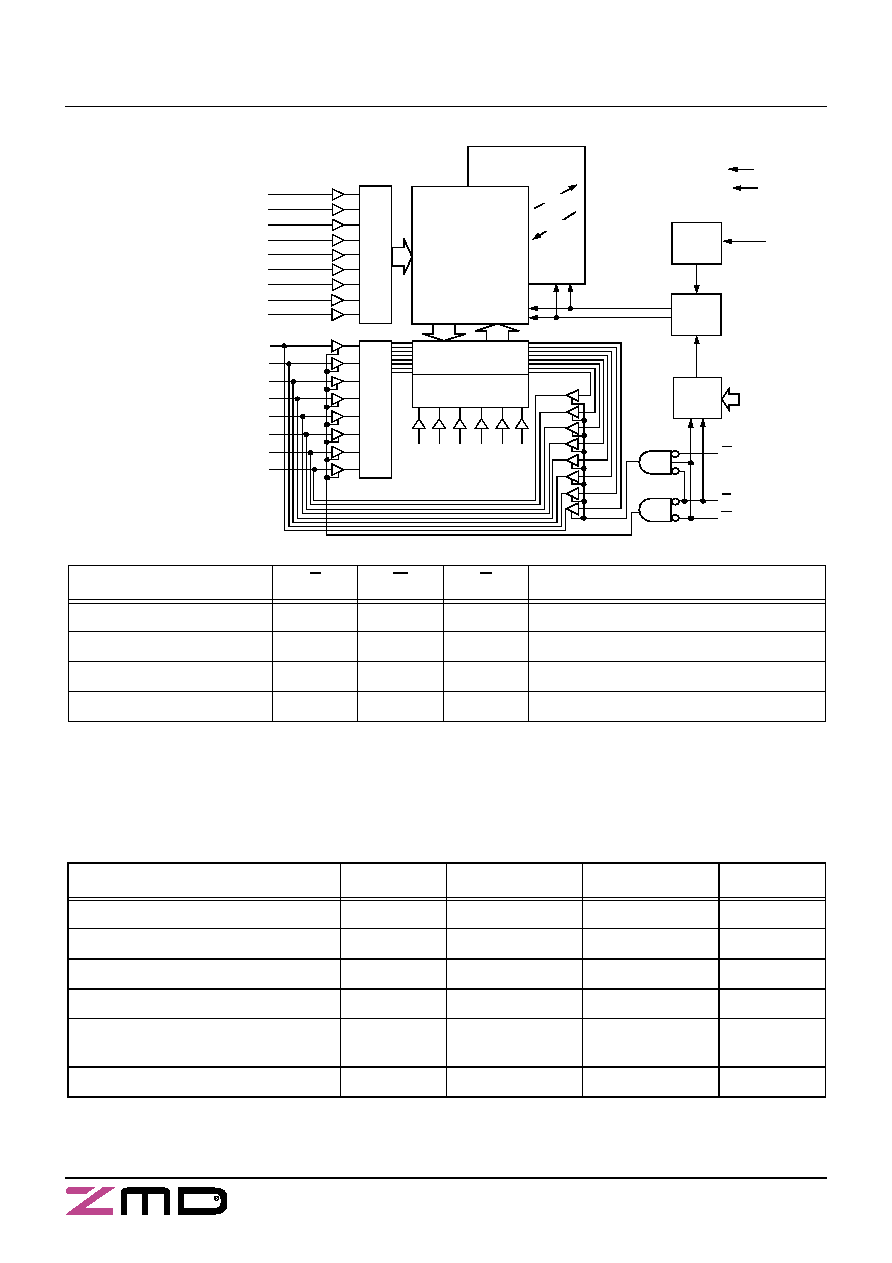
EEPROM Array
512 x (64 x 8)
STORE
RECALL
SRAM
Array
512 Rows x
64 x 8 Columns
A5
A6
A7
A8
A9
A11
A12
A13
DQ0
DQ1
DQ2
DQ3
DQ4
DQ5
DQ6
DQ7
Column I/O
Column Decoder
Ro
w De
c
o
d
e
r
V
CC
V
SS
V
CC
G
E
W
A0 A1
A2
A3
A4 A10
Software
Detect
A0 - A13
A14
In
p
u
t B
u
ffe
r
s
Store/
Recall
Control
Power
Control
Operating Mode
E
W
G
DQ0 - DQ7
Standby/not selected
H
*
*
High-Z
Internal Read
L
H
H
High-Z
Read
L
H
L
Data Outputs Low-Z
Write
L
L
*
Data Inputs High-Z
Truth Table forSRAM Operations
Block Diagram
Absolute Maximum Ratings
a
Symbol
Min.
Max.
Unit
Power Supply Voltage
V
CC
-0.5
7
V
Input Voltage
V
I
-0.3
V
CC
+0.5
V
Output Voltage
V
O
-0.3
V
CC
+0.5
V
Power Dissipation
P
D
1
W
Operating Temperature
C-Type
K-Type
T
a
0
-40
70
85
∞C
∞C
Storage Temperature
T
stg
-65
150
∞C
Characteristics
All voltages are referenced to V
SS
= 0 V (ground).
All characteristics are valid in the power supply voltage range and in the operating temperature range specified.
Dynamic measurements are based on a rise and fall time of
5 ns, measured between 10 % and 90 % of V
I
, as well as
input levels of V
IL
= 0 V and V
IH
= 3 V. The timing reference level of all input and output signals is 1.5 V,
with the exception of the t
dis
-times and t
en
-times, in which cases transition is measured
± 200 mV from steady-state voltage.
*
H or L
a: Stresses greater than those listed under ,,Absolute Maximum Ratings" may cause permanent damage to the device. This is a stress
rating only, and functional operation of the device at condition above those indicated in the operational sections of this specification is
not implied. Exposure to absolute maximum rating conditions for extended periods may affect reliability.
3
December 05, 2003
U637H256
Preliminary
DC Characteristics
Symbol
Conditions
C-Type
K-Type
Unit
Min.
Max.
Min.
Max.
Operating Supply Current
b
I
CC1
V
CC
V
IL
V
IH
t
c
= 5.5 V
= 0.8 V
= 2.2 V
= 25 ns
95
100
mA
Average Supply Current during
c
STORE
I
CC2
V
CC
E
W
V
IL
V
IH
= 5.5 V
0.2 V
V
CC
-0.2 V
0.2 V
V
CC
-0.2 V
6
7
mA
Operating Supply Current
b
at t
cR
= 200 ns
(Cycling CMOS Input Levels)
I
CC3
V
CC
W
V
IL
V
IH
= 5.5 V
V
CC
-0.2 V
0.2 V
V
CC
-0.2 V
20
20
mA
Standby Supply Current
d
(Cycling TTL Input Levels)
I
CC(SB)1
V
CC
E
t
c
= 5.5 V
= V
IH
= 25 ns
40
42
mA
Standby Supply Curent
d
(Stable CMOS Input Levels)
I
CC(SB)
V
CC
E
V
IL
V
IH
= 5.5 V
V
CC
-0.2 V
0.2 V
V
CC
-0.2 V
3
3
mA
Recommended
Operating Conditions
Symbol
Conditions
Min.
Max.
Unit
Power Supply Voltage
V
CC
4.5
5.5
V
Input Low Voltage
V
IL
-2 V at Pulse Width
10 ns permitted
-0.3
0.8
V
Input High Voltage
V
IH
2.2
V
CC
+0.3
V
b: I
CC1
and I
CC3
are depedent on output loading and cycle rate. The specified values are obtained with outputs unloaded.
The current I
CC1
is measured for WRITE/READ - ratio of 1/2.
c: I
CC2
is the average current required for the duration of the SoftStore STORE cycle.
d: Bringing E
V
IH
will not produce standby current levels until a software initiated nonvolatile cycle in progress has timed out.
See MODE SELECTION table. The current I
CC(SB)1
is measured for WRITE/READ - ratio of 1/2.
4
December 05, 2003
U637H256
Preliminary
DC Characteristics
Symbol
Conditions
C-Type
K-Type
Unit
Min.
Max.
Min.
Max.
Output High Voltage
Output Low Voltage
V
OH
V
OL
V
CC
I
OH
I
OL
= 4.5 V
=-4 mA
= 8 mA
2.4
0.4
2.4
0.4
V
V
Output High Current
Output Low Current
I
OH
I
OL
V
CC
V
OH
V
OL
= 4.5 V
= 2.4 V
= 0.4 V
8
-4
8
-4
mA
mA
Input Leakage Current
High
Low
I
IH
I
IL
V
CC
V
IH
V
IL
= 5.5 V
= 5.5 V
= 0 V
-1
1
-1
1
µA
µA
Output Leakage Current
High at Three-State- Output
Low at Three-State- Output
I
OHZ
I
OLZ
V
CC
V
OH
V
OL
= 5.5 V
= 5.5 V
= 0 V
-1
1
-1
1
µA
µA
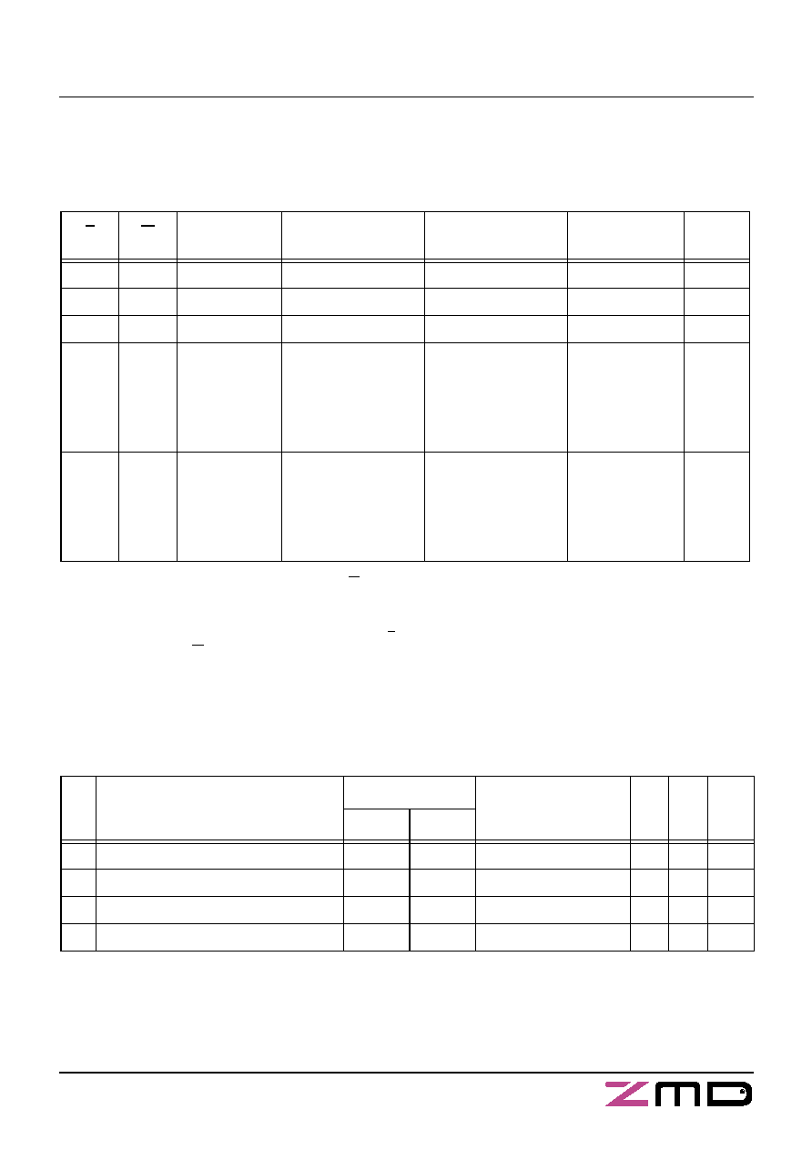
SRAM Memory Operations
No.
Switching Characteristics
Read Cycle
Symbol
Min.
Max.
Unit
Alt.
IEC
1
Read Cycle Time
f
t
AVAV
t
cR
25
ns
2
Address Access Time to Data Valid
g
t
AVQV
t
a(A)
25
ns
3
Chip Enable Access Time to Data Valid
t
ELQV
t
a(E)
25
ns
4
Output Enable Access Time to Data Valid
t
GLQV
t
a(G)
10
ns
5
E HIGH to Output in High-Z
h
t
EHQZ
t
dis(E)
10
ns
6
G HIGH to Output in High-Z
h
t
GHQZ
t
dis(G)
10
ns
7
E LOW to Output in Low-Z
t
ELQX
t
en(E)
5
ns
8
G LOW to Output in Low-Z
t
GLQX
t
en(G)
0
ns
9
Output Hold Time after Address Change
t
AXQX
t
v(A)
3
ns
10 Chip Enable to Power Active
e
t
ELICCH
t
PU
0
ns
11 Chip Disable to Power Standby
d, e
t
EHICCL
t
PD
25
ns
e: Parameter guaranteed but not tested.
f:
Device is continuously selected with E and G both Low.
g: Address valid prior to or coincident with E transition LOW.
h: Measured
± 200 mV from steady state output voltage.

5
December 05, 2003
U637H256
Preliminary
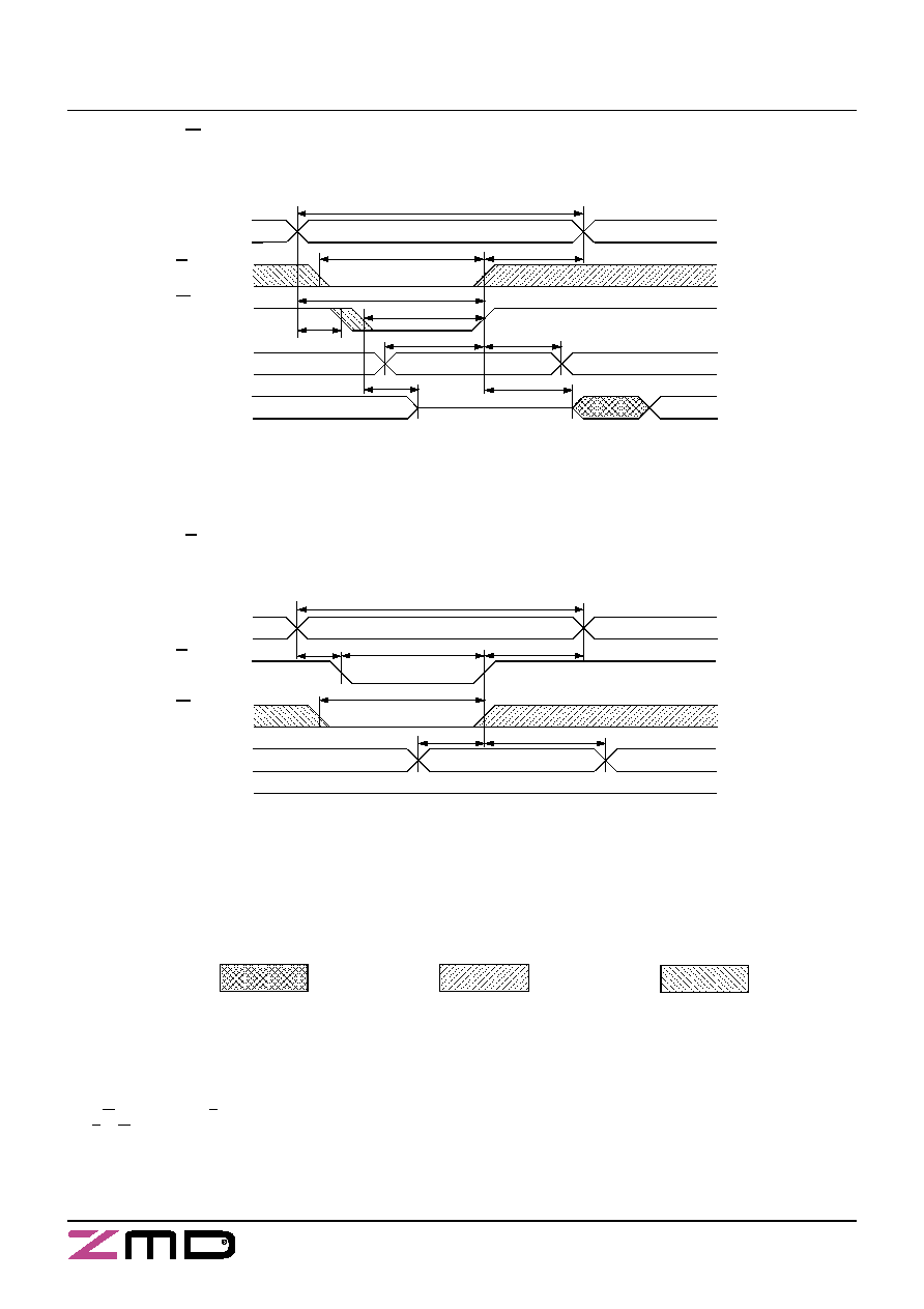
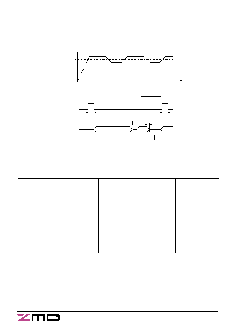
Read Cycle 1: Ai-controlled (during Read cycle: E = G = V
IL
, W = V
IH
)
f
Read Cycle 2: G-, E-controlled (during Read cycle: W = V
IH
)
g
No.
Switching Characteristics
Write Cycle
Symbol
Min.
Max.
Unit
Alt. #1 Alt. #2
IEC
12 Write Cycle Time
t
AVAV
t
AVAV
t
cW
25
ns
13 Write Pulse Width
t
WLWH
t
w(W)
20
ns
14 Write Pulse Width Setup Time
t
WLEH
t
su(W)
20
ns
15 Address Setup Time
t
AVWL
t
AVEL
t
su(A)
0
ns
16 Address Valid to End of Write
t
AVWH
t
AVEH
t
su(A-WH)
20
ns
17 Chip Enable Setup Time
t
ELWH
t
su(E)
20
ns
18 Chip Enable to End of Write
t
ELEH
t
w(E)
20
ns
19 Data Setup Time to End of Write
t
DVWH
t
DVEH
t
su(D)
10
ns
20 Data Hold Time after End of Write
t
WHDX
t
EHDX
t
h(D)
0
ns
21 Address Hold after End of Write
t
WHAX
t
EHAX
t
h(A)
0
ns
22 W LOW to Output in High-Z
h, i
t
WLQZ
t
dis(W)
10
ns
23 W HIGH to Output in Low-Z
t
WHQX
t
en(W)
5
ns
t
a(A)
Previous Data Valid
Output Data Valid
t
cR
Address Valid
t
v(A)
Ai
DQi
Output
(1)
(2)
(9)
Ai
E
G
t
dis(E)
t
cR
t
a(E)
t
en(E)
t
en(G)
t
a(G)
t
dis(G)
Address Valid
Output Data Valid
I
CC
ACTIVE
STANDBY
t
PD
t
PU
(1)
(3)
(4)
(5)
(7)
(6)
(8)
(10)
(11)
t
a(A)
(2)
High Impedance
DQi
Output
6
December 05, 2003
U637H256
Preliminary
(15)
L- to H-level
undefined
H- to L-level
i:
If W is low and when E goes low, the outputs remain in the high impedance state.
j:
E or W must be V
IH
during address transition.
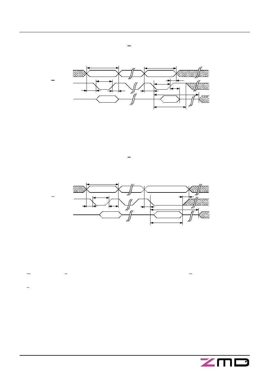
Write Cycle #1: W-controlled
j
Write Cycle #2: E-controlled
j
t
h(D)
Ai
E
W
DQi
Input
DQi
Output
t
cW
t
su(E)
t
h(A
)
t
w(W)
t
su(D)
t
dis(W)
t
en(W)
Address Valid
Input Data Valid
High Impedance
t
su(A-WH)
(12)
(16)
(13)
(19)
(20)
(23)
(21)
t
su(A)
t
h(D)
Ai
E
W
DQi
Input
DQi
Output
t
cW
t
w(E)
t
h(A)
t
su(D)
Address Valid
Input Data Valid
t
su(W)
(12)
(18)
(21)
(20)
(19)
(17)
(22)
Previous Data Valid
(14)
High Impedance
(15)
t
su(A)
7
December 05, 2003
U637H256
Preliminary
Nonvolatile Memory Operations
Mode Selection
E
W
A13 - A0
(hex)
Mode
I/O
Power
Notes
H
X
X
Not Selected
Output High Z
Standby
L
H
X
Read SRAM
Output Data
Active
m
L
L
X
Write SRAM
Input Data
Active
L
H
0E38
31C7
03E0
3C1F
303F
0FC0
Read SRAM
Read SRAM
Read SRAM
Read SRAM
Read SRAM
Nonvolatile STORE
Output Data
Output Data
Output Data
Output Data
Output Data
Output High Z
Active
k, l
k, l
k, l
k, l
k, l
k, l
L
H
0E38
31C7
03E0
3C1F
303F
0C63
Read SRAM
Read SRAM
Read SRAM
Read SRAM
Read SRAM
Nonvolatile RECALL
Output Data
Output Data
Output Data
Output Data
Output Data
Output High Z
Active
k, l
k, l
k, l
k, l
k, l
k, l
k: The six consecutive addresses must be in order listed. W must be high during all six consecutive cycles. See STORE cycle and RECALL
cycle tables and diagrams for further details.
The following six-address sequence is used for testing purposes and should not be used: 0E38, 31C7, 03E0, 3C1F, 303F, 339C.
l:
While there are 15 addresses on the U637H256, only the lower 14 are used to control software modes.
Activation of nonvolatile cycles does not depend on the state of G.
m: I/O state assumes that G
V
IL
.
No.
PowerStore
Power Up RECALL
Symbol
Conditions
Min. Max. Unit
Alt.
IEC
24 Power Up RECALL Duration
n
t
RESTORE
650
µs
25 STORE Cycle Duration
f, e
t
PDSTORE
10
ms
26 Time allowed to Complete SRAM Cycle
f
t
DELAY
1
µs
Low Voltage Trigger Level
V
SWITCH
4.0
4.5
V
n: t
RESTORE
starts from the time V
CC
rises above V
SWITCH
.
8
December 05, 2003
U637H256
Preliminary
No.
Software Controlled STORE/RECALL
Cycle
k, o
Symbol
Min.
Max.
Unit
Alt.
IEC
27 STORE/RECALL Initiation Time
t
AVAV
t
cR
25
ns
28 Chip Enable to Output Inactive
p
t
ELQZ
t
dis(E)SR
600
ns
29 STORE Cycle Time
q
t
ELQXS
t
d(E)S
10
ms
30 RECALL Cycle Time
r
t
ELQXR
t
d(E)R
20
µs
31 Address Setup to Chip Enable
s
t
AVELN
t
su(A)SR
0
ns
32 Chip Enable Pulse Width
s, t
t
ELEHN
t
w(E)SR
20
ns
33 Chip Disable to Address Change
s
t
EHAXN
t
h(A)SR
0
ns
PowerStore and automatic Power Up RECALL
V
CC
5.0 V
t
PowerStore
Power Up
V
SWITCH
W
DQi
POWER UP
RECALL
BROWN OUT
t
RESTORE
t
RESTORE
BROWN OUT
PowerStore
(NO SRAM WRITES)
RECALL
(24)
(24)
NO STORE
t
PDSTORE
t
DELAY
(25)
o: The software sequence is clocked with E controlled READs.
p: Once the software controlled STORE or RECALL cycle is initiated, it completes automatically, ignoring all inputs.
q: Note that STORE cycles (but not RECALL) are inhibited by V
CC
< V
SWITCH
(STORE inhibit).
r: An automatic RECALL also takes place at power up, starting when V
CC
exceeds V
SWITCH
and takes t
RESTORE
. V
CC
must not drop below
V
SWITCH
once it has been exceeded for the RECALL to function properly.
s: Noise on the E pin may trigger multiple READ cycles from the same address and abort the address sequence.
t:
If the Chip Enable Pulse Width is less than t
a(E)
(see Read Cycle) but greater than or equal t
w(E)SR
, than the data may not be valid at
the end of the low pulse, however the STORE or RECALL will still be initiated.
9
December 05, 2003
U637H256
Preliminary
u: W must be HIGH when E is LOW during the address sequence in order to initiate a nonvolatile cycle. G may be either HIGH or LOW
throughout. Addresses 1 through 6 are found in the mode selection table. Address 6 determines wheter the U637H256 performs a STORE
or RECALL.
v: E must be used to clock in the address sequence for the Software controlled STORE and RECALL cycles.
Ai
E
DQi
Output
t
cR
t
w(E)SR
High Impedance
ADDRESS 1
VALID
VALID
Software Controlled STORE/RECALL Cycle
s, t, u, v
(E = HIGH after STORE initiation)
ADDRESS 6
t
cR
(27)
(27)
t
h(A)SR
(33)
(32)
t
su(A)SR
(31)
Ai
E
DQi
Output
t
cR
t
w(E)SR
High Impedance
ADDRESS 1
VALID
VALID
ADDRESS 6
t
d(E)S
(29)
(30)
(27)
t
h(A)SR
(33)
(32)
t
su(A)SR
(31)
t
dis(E)SR
(28)
t
h(A)SR
(33)
t
su(A)SR
(31)
t
w(E)SR
t
h(A)SR
(33)
(32)
(31)
(5)
t
dis(E)
Software Controlled STORE/RECALL Cycle
s, t, u, v
(E = LOW after STORE initiation)
t
d(E)S
(29)
(30)
t
dis(E)SR
(28)
t
d(E)R
t
d(E)R
t
su(A)SR
10
December 05, 2003
U637H256
Preliminary
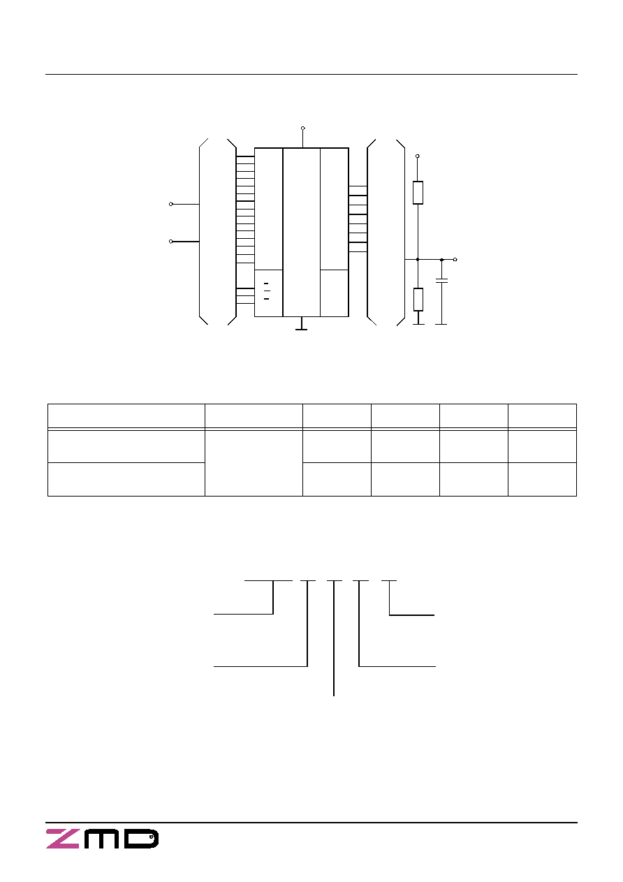
Test Configuration for Functional Check
V
IH
V
IL
V
SS
480
255
30 pF
w
V
O
S
i
m
u
lt
an
eo
us
m
e
as
ur
e
-
m
e
n
t
of
al
l
8
ou
t
p
ut
pi
ns
I
n
pu
t
le
ve
l ac
cor
d
in
g t
o
t
h
e
r
e
l
e
va
nt
t
e
st
me
asu
r
em
en
t
DQ0
DQ1
DQ2
DQ3
DQ4
DQ5
DQ6
DQ7
A0
A1
A2
A3
A4
A5
A6
A7
A8
A9
A10
A11
A12
E
W
G
5 V
A13
A14
V
CC
x
w: In measurement of t
dis
-times and t
en
-times the capacitance is 5 pF.
x: Between V
CC
and V
SS
must be connected a high frequency bypass capacitor 0.1
µF to avoid disturbances.
Capacitance
e
Conditions
Symbol
Min.
Max.
Unit
Input Capacitance
V
CC
V
I
f
T
a
= 5.0 V
= V
SS
= 1 MHz
= 25
∞C
C
I
8
pF
Output Capacitance
C
O
7
pF
All Pins not under test must be connected with ground by capacitors.
U637H256 D1
C
25
Type
Package
D1 = PDIP28 (600 mil)
Operating Temperature Range
C = 0 to 70 ∞C
K =
-40 to 85∞C
Access Time
25 = 25 ns
IC Code Numbers
The date of manufacture is given by the last 4 digits of the mark, the first 2 digits indicating the year, and the last 2
digits the calendar week.
Internal Code

11
December 05, 2003
U637H256
Preliminary
Device Operation
The U637H256 has two separate modes of operation:
SRAM mode and nonvolatile mode. The memory ope-
rates in SRAM mode as a standard fast static RAM.
Data is transferred in nonvolatile mode from SRAM to
EEPROM (the STORE operation) or from EEPROM to
SRAM (the RECALL operation). In this mode SRAM
functions are disabled.
STORE cycles may be initiated under user control via a
software sequence and are also automatically initiated
when the power supply voltage level of the chip falls
below V
SWITCH
. RECALL operations are automatically
initiated upon power up and may also occur when the
V
CC
rises above V
SWITCH
, after a low power condition.
RECALL cycles may also be initiated by a software
sequence.
SRAM READ
The U637H256 performs a READ cycle whenever E
and G are LOW and W is HIGH. The address specified
on pins A0 - A14 determines which of the 32768 data
bytes will be accessed. When the READ is initiated by
an address transition, the outputs will be valid after a
delay of t
cR
. If the READ is initiated by E or G, the out-
puts will be valid at t
a(E)
or at t
a(G)
, whichever is later.
The data outputs will repeatedly respond to address
changes within the t
cR
access time without the need for
transition on any control input pins, and will remain
valid until another address change or until E or G is
brought HIGH or W is brought LOW.
SRAM WRITE
A WRITE cycle is performed whenever E and W are
LOW. The address inputs must be stable prior to
entering the WRITE cycle and must remain stable until
either E or W goes HIGH at the end of the cycle. The
data on pins DQ0 - 7 will be written into the memory if it
is valid t
su(D)
before the end of a W controlled WRITE or
t
su(D)
before the end of an E controlled WRITE.
It is recommended that G is kept HIGH during the
entire WRITE cycle to avoid data bus contention on the
common I/O lines. If G is left LOW, internal circuitry will
turn off the output buffers t
dis (W)
after W goes LOW.
Automatic STORE
During normal operation, the U637H256 will draw cur-
rent from V
CC
to charge up an integrated capacitor.
This stored charge will be used by the chip to perform a
single STORE operation. If the voltage on the V
CC
pin
drops below V
SWITCH
, the part will automatically discon-
nect the internal components from the external power
supply with a typical delay of 150 ns and initiate a
STORE operation with t
PDSTORE
max. 10 ms.
In order to prevent unneeded STORE operations, auto-
matic STORE will be ignored unless at least one
WRITE operation has taken place since the most
recent STORE or RECALL cycle. Software initiated
STORE cycles are performed regardless of whether or
not a WRITE operation has taken place.
SRAM READ and WRITE operations that are in pro-
gress after an automatic STORE cycle on power down
is requested are given time to complete before the
STORE operation is initiated.
During t
DELAY
multiple SRAM READ operations may
take place. If a WRITE is in progress it will be allowed a
time, t
DELAY
, to complete. Any SRAM WRITE cycles
requested after the V
CC
pin drops below V
SWITCH
will be
inhibited.
Automatic RECALL
During power up, an automatic RECALL takes place.
At a low power condition (power supply voltage <
V
SWITCH
) an internal RECALL request may be latched.
As soon as power supply voltage exceeds the sense
voltage of V
SWITCH
, a requested RECALL cycle will
automatically be initiated and will take t
RESTORE
to com-
plete.
If the U637H256 is in a WRITE state at the end of
power up RECALL, the SRAM data will be corrupted.
To help avoid this situation, a 10 k
resistor should be
connected between W and power supply voltage.
Software Nonvolatile STORE
The U637H256 software controlled STORE cycle is
initiated by executing sequential READ cycles from six
specific address locations. By relying on READ cycles
only, the U637H256 implements nonvolatile operation
while remaining compatible with standard 32K x 8
SRAMs. During the STORE cycle, an erase of the pre-
vious nonvolatile data is performed first, followed by a
parallel programming of all the nonvolatile elements.
Once a STORE cycle is initiated, further inputs and out-
puts are disabled until the cycle is completed.
Because a sequence of addresses is used for STORE
initiation, it is important that no other READ or WRITE
accesses intervene in the sequence or the sequence
will be aborted.
To initiate the STORE cycle the following READ
sequence must be performed:
1.
Read addresses 0E38 (hex) Valid READ
2.
Read addresses 31C7 (hex) Valid READ
3.
Read addresses 03E0 (hex) Valid READ
4.
Read addresses 3C1F (hex) Valid READ
5.
Read addresses 303F (hex) Valid READ
6.
Read addresses 0FC0 (hex) Initiate STORE
Cycle

12
December 05, 2003
U637H256
Preliminary
Once the sixth address in the sequence has been
entered, the STORE cycle will commence and the chip
will be disabled. It is important that READ cycles and
not WRITE cycles be used in the sequence, although it
is not necessary that G be LOW for the sequence to be
valid. After the t
STORE
cycle time has been fulfilled, the
SRAM will again be activated for READ and WRITE
operation. When V
CC
< V
SWITCH
all software STORE
operations will be inhibited.
Any SRAM WRITE cycles requested after the V
CC
pin
drops below V
SWITCH
will be inhibited.
Software Nonvolatile RECALL
A RECALL cycle of the EEPROM data into the SRAM
is initiated with a sequence of READ operations in a
manner similar to the STORE initiation. To initiate the
RECALL cycle the following sequence of READ opera-
tions must be performed:
1.
Read addresses 0E38 (hex) Valid READ
2.
Read addresses 31C7 (hex) Valid READ
3.
Read addresses 03E0 (hex) Valid READ
4.
Read addresses 3C1F (hex) Valid READ
5.
Read addresses 303F (hex) Valid READ
6.
Read addresses 0C63 (hex) Initiate RECALL
Cycle
Internally, RECALL is a two step procedure. First, the
SRAM data is cleared and second, the nonvolatile
information is transferred into the SRAM cells. After
t
d(E)R
cycle time the SRAM will once again be ready for
READ and WRITE operations.The RECALL operation
in no way alters the data in the EEPROM cells. The
nonvolatile data can be recalled an unlimited number of
times.
Low Average Active Power
The U637H256 has been designed to draw significantly
less power when E is LOW (chip enabled) but the
access cycle time is longer than 55 ns.
When E is HIGH the chip consumes only standby cur-
rent.
The overall average current drawn by the part depends
on the following items:
1. CMOS or TTL input levels
2. the time during which the chip is disabled (E HIGH)
3. the cycle time for accesses (E LOW)
4. the ratio of READs to WRITEs
5. the operating temperature
6. the V
CC
level
The information describes the type of component and shall not be considered as assured characteristics.
Terms of delivery and rights to change design reserved.

Zentrum Mikroelektronik Dresden AG
Grenzstraþe 28
∑ D-01109 Dresden ∑ P. O. B. 80 01 34 ∑ D-01101 Dresden ∑ Germany
Phone: +49 351 8822 306
∑ Fax: +49 351 8822 337 ∑ Email: memory@zmd.de ∑ http://www.zmd.de
December 05, 2003
U637H256
Preliminary
LIFE SUPPORT POLICY
ZMD products are not designed, intended, or authorized for use as components in systems intended for surgical
implant into the body, or other applications intended to support or sustain life, or for any other application in which
the failure of the ZMD product could create a situation where personal injury or death may occur.
Components used in life-support devices or systems must be expressly authorized by ZMD for such purpose.
LIMITED WARRANTY
The information in this document has been carefully checked and is believed to be reliable. However Zentrum Mikro-
elektronik Dresden AG (ZMD) makes no guarantee or warranty concerning the accuracy of said information and
shall not be responsible for any loss or damage of whatever nature resulting from the use of, or reliance upon it. The
information in this document describes the type of component and shall not be considered as assured characteri-
stics.
ZMD does not guarantee that the use of any information contained herein will not infringe upon the patent, trade-
mark, copyright, mask work right or other rights of third parties, and no patent or licence is implied hereby. This
document does not in any way extent ZMD's warranty on any product beyond that set forth in its standard terms and
conditions of sale.
ZMD reserves terms of delivery and reserves the right to make changes in the products or specifications, or both,
presented in this publication at any time and without notice.
Zentrum Mikroelektronik Dresden AG
Grenzstraþe 28
∑ D-01109 Dresden ∑ P. O. B. 80 01 34 ∑ D-01101 Dresden ∑ Germany
Phone: +49 351 8822 306
∑ Fax: +49 351 8822 337 ∑ Email: sales@zmd.de ∑ http://www.zmd.de
November 01, 2001
U637H256
Preliminary