
1
December 12, 1997
UL6264A
F
Packages: PDIP28(600 mil)
SOP28 (330 mil)
Description
The UL6264A is a static RAM
manufactured using a CMOS pro-
cess technology with the following
operating modes:
- Read - Standby
- Write - Data Retention
The memory array is based on a
6-transistor cell.
The circuit is activated by the rising
edge of E2 (at E1 = L) or the falling
edge of E1 (at E2 = H). The
address and control inputs open
simultaneously. According to the
information of W and G the data
inputs, or outputs, are active. In the
active state E1 = L and E2 = H,
each address change leads to a
new Read or Write cycle. In a Read
cycle, the data outputs are activa-
ted by the falling edge of G, after-
wards the data word read will be
available at the outputs
DQ0 - DQ7. After the address
change, the data outputs go High-Z
until the new read information is
available. The data outputs have no
preferred state. If the memory is
driven by CMOS levels in the active
state, and if there is no change of
the address, data input and control
signals W or G, the operating cur-
rent (at I
O
= 0 mA) drops to the
value of the operating current in the
Standby mode. The Read cycle is
finished by the falling edge of E2 or
W, or by the rising edge of E1,
respectively.
Data retention is guaranteed down
to 2 V.
With the exception of E2, all inputs
consist of NOR gates, so that no
pull-up/pull-down resistors are
required. This gate circuit allows to
achieve low power standby require-
ments by activation with TTL-levels
too.
If the circuit is inactivated by E2 = L,
the standby current (TTL) drops to
100
µ
A typ.
Features
F
8192 x 8 bit static CMOS RAM
F
250 and 500 ns Access Times
F
Common data inputs and data
outputs
F
Three-state outputs
F
Typ. operating supply current:
250 ns: 12 mA
500 ns: 7 mA
F
Standby current < 5
µ
A
F
Standby current at 25
∞
C
and 3.3 V: typ. 50 nA
F
TTL/CMOS-compatible
F
Automatic reduction of power
dissipation in long Read or Write
cycles
F
Power supply voltage 3.3 V
F
Operating temperature ranges
0 to 70
∞
C
-25 to 85
∞
C
-40 to 85
∞
C
F
Quality assessment according to
CECC 90000, CECC 90100 and
CECC 90111
F
ESD protection > 2000 V
(MIL STD 883C M3015.7)
F
Latch-up immunity > 100 mA
Low Voltage 8K x 8 SRAM
Pin Description
Signal Name Signal Description
A0 - A12 Address Inputs
DQ0 - DQ7 Data In/Out
E1
Chip Enable 1
E2 Chip Enable 2
G
Output Enable
W
Write Enable
VCC Power Supply Voltage
VSS Ground
n.c. not connected
Pin Configuration
1
n.c.
VCC
28
2
A12
W (WE)
27
4
A6
A8
25
5
A5
A9
24
3
A7
E2 (CE2)
26
6
A4
A11
23
7
A3
G (OE)
22
8
A2
A10
21
12
DQ1
DQ5
17
9
A1
E (CE1)
20
10
A0
DQ7
19
11
DQ0
DQ6
18
13
DQ2
DQ4
16
14
VSS
DQ3
15
PDIP
Top View
SOP
2
December 12, 1997
UL6264A
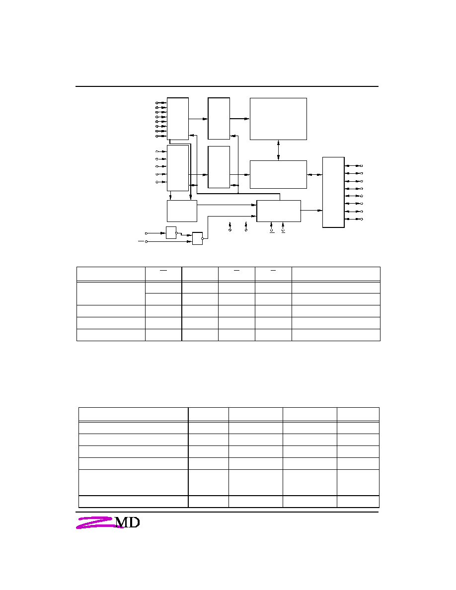
Address
Change
Detector
* H or L
Operating Mode E1
E2 W
G
DQ0 - DQ7
Standby/not
selected
*
L
*
*
High-Z
H
*
*
*
High-Z
Internal Read L H H H High-Z
Read L H H L Data Outputs Low-Z
Write L H L * Data Inputs High-Z
Truth Table
A0
A1
A2
A3
A10
Memory Cell
Array
256 Rows x
256 Columns
R
o
w
D
e
c
oder
R
o
w
A
ddr
es
s
I
nput
s
C
o
l
u
m
n
D
e
c
oder
C
o
m
m
on D
a
t
a
-
I
/
O
Sense Amplifier/
Write Control Logic
Clock
Generator
1
DQ0
DQ1
DQ2
DQ3
DQ4
DQ5
DQ6
DQ7
Maximum Ratings Symbol Min. Max. Unit
Power Supply Voltage V
CC
-0.3 7 V
Input Voltage V
I
-0.3 V
CC
+ 0.5 V
Output Voltage V
O
-0.3 V
CC
+ 0.5 V
Power Dissipation P
D
1
W
Operating
Temperature
C-Type
G-Type
K-Type
T
a
0
-25
-40
70
85
85
∞
C
∞
C
∞
C
Storage Temperature T
stg
-55 125
∞
C
E2
E1
Characteristics
C
o
l
u
m
n
Addr
es
s
I
nput
s
V
CC
V
SS
W
G
Block Diagram
A4
A5
A6
A7
A8
A9
A11
A12
All voltages are referenced to V
SS
= 0 V (ground).
All characteristics are valid in the power supply voltage range and in the operating temperature range specified.
Dynamic measurements are based on a rise and fall time of
5 ns, measured between 10 % and 90 % of V
I
, as well as
input levels of V
IL
= 0 V and V
IH
= 3 V. The timing reference level of all input and output signals is 1.5 V,
with the exception of the t
dis
-times, in which cases transition is measured
±
200 mV from steady-state voltage.
3
December 12, 1997
UL6264A
Electrical Characteristics Symbol Conditions Min. Max. Unit
Supply Current - Operating Mode
Supply Current - Standby Mode
(CMOS level)
Supply Current - Standby Mode
(TTL level)
I
CC(OP)
I
CC(SB)
I
CC(SB)1
V
CC
V
IL
V
IH
t
cW
t
cW
V
CC
V
E1
= V
E2
V
CC
V
E1
= V
E2
= 3.6 V
= 0.8 V
= 2.0 V
= 500 ns
= 250 ns
= 3.6 V
= V
CC
-
0.2
V
= 3.6 V
= 2.0 V
20
30
5
2
(typ. 0.7)
mA
mA
µ
A
mA
Output High Voltage
Output Low Voltage
V
OH
V
OL
V
CC
I
OH
V
CC
I
OL
= 3.0 V
= -1.0 mA
= 3.0 V
= 2.0 mA
2.4
0.4
V
V
Input High Leakage Current
Input Low Leakage Current
I
IH
I
IL
V
CC
V
IH
V
CC
V
IL
= 3.6 V
= 3.6 V
= 3.6 V
=
0 V
-1
1
µ
A
µ
A
Output High Current
Output Low Current
I
OH
I
OL
V
CC
V
OH
V
CC
V
OL
= 3.0 V
= 2.4 V
= 3.0 V
= 0.4 V
2.0
-1 mA
mA
Output Leakage Current
High at Three-State Outputs
Low at Three-State Outputs
I
OHZ
I
OLZ
V
CC
V
OH
V
CC
V
OL
= 3.6 V
= 3.6 V
= 3.6 V
=
0 V
-1
1
µ
A
µ
A
Recommended Operating
Conditions
Symbol Conditions Min. Max. Unit
Power Supply Voltage V
CC
3.0 3.6 V
Data Retention Voltage V
CC(DR)
2.0 V
Input Low Voltage* V
IL
-0.3 0.8 V
Input High Voltage V
IH
2.0 V
CC
+ 0.3 V
* -2 V at Pulse Width 10 ns
4
December 12, 1997
UL6264A
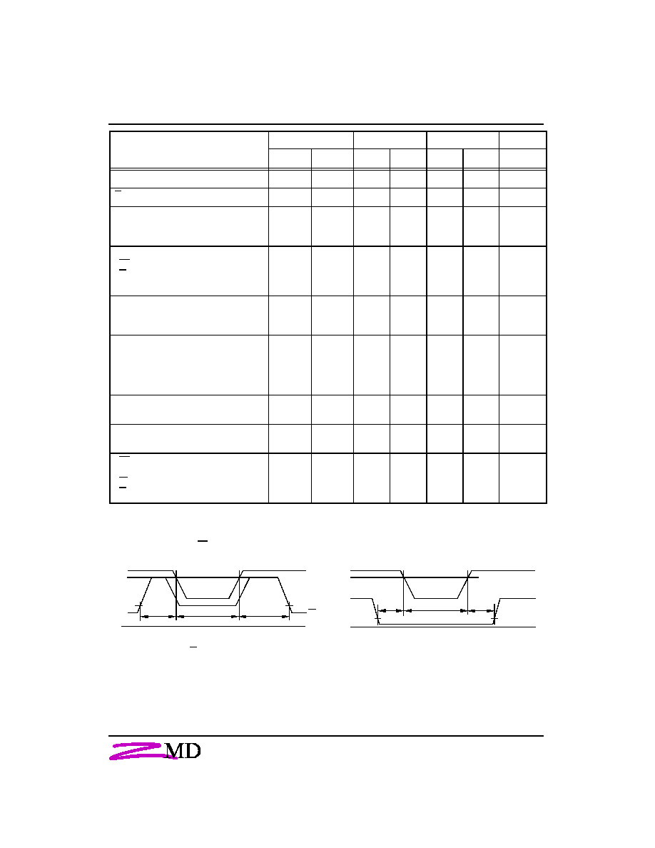
Switching Characteristics
Symbol Min. Max. Unit
Alt.
IEC
25
50
25
50
Time to Output in Low-Z t
LZ
t
t(QX)
20 20 ns
G LOW to Output in Low-Z t
OLZ
t
tG(QX)
10 10 ns
Cycle Time
Write Cycle Time
Read Cycle Time
t
WC
t
RC
t
cW
t
cR
250
250
500
500
ns
ns
Access Time
E1 LO W or E2 HIGH to Data Valid
G LO W to Data Valid
Address to Data Valid
t
ACE
t
OE
t
AA
t
a(E)
t
a(G)
t
a(A)
-
-
-
-
-
-
250
100
250
500
100
500
ns
ns
ns
Pulse Widths
Write Pulse Width
Chip Enable to End of Write
t
WP
t
CW
t
w(W)
t
w(E)
120
180
150
210
ns
ns
Setup Times
Address Setup Time
Chip Enable to End of Write
Write Pulse Width
Data Setup Time
t
AS
t
CW
t
WP
t
DS
t
su(A)
t
su(E)
t
su(W)
t
su(D)
0
180
120
80
0
210
150
100
ns
ns
ns
ns
Data Hold Time
Address Hold Time from End of Write
t
DH
t
AH
t
h(D)
t
h(A)
0
0
0
0
ns
ns
Output Hold Time from Address
Change
t
OH
t
v(A)
20 20 ns
E1 HIGH or E2 LOW to Output in
High-Z
W LOW to Output in High-Z
G HIGH to Output in High-Z
t
HZCE
t
HZWE
t
HZOE
t
dis(E)
t
dis(W)
t
dis(G)
0
0
0
0
0
0
60
60
40
60
60
40
ns
ns
ns
V
CC(DR)
2 V
Data Retention Mode E1-Controlled
Data Retention Mode E2-Controlled
Data Retention
3.0 V
t
DR
t
rec
V
CC
E1
V
CC(DR)
2 V
V
E2(DR)
V
CC(DR)
- 0.2 V or V
E2(DR)
0.2 V
V
CC(DR)
- 0.2 V
V
E1(DR)
V
CC(DR)
+ 0.3 V
0 V
Data Retention
t
rec
t
DR
0.8 V
0.8 V V
E2(DR)
0.2 V
2.0 V
2.0 V
3.0 V
0 V
V
CC
E2
Chip Deselect to Data Retention Time t
DR
:
min 0 ns
Operating Recovery Time t
rec
:
min t
cR
5
December 12, 1997
UL6264A
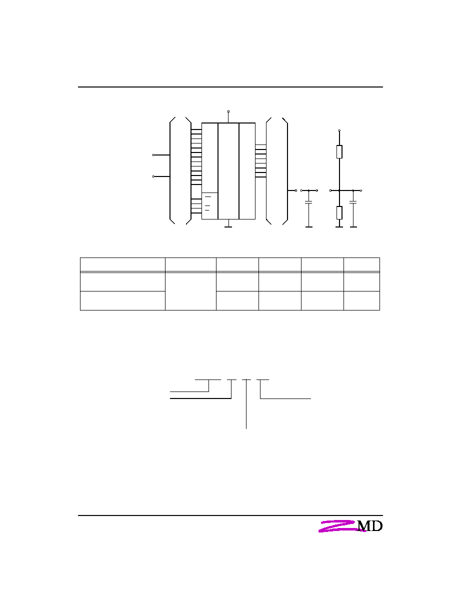
Test Configuration for Functional Check
V
IH
V
IL
V
SS
V
CC
3.3 V
960
510
5 pF
V
O
Si
m
u
l
t
aneou
s
M
eas
ur
e-
m
e
n
t
of
al
l
8 out
put
p
i
ns
I
n
p
u
t
l
e
v
e
l
ac
c
o
r
d
i
ng
t
o
t
he
r
e
l
e
v
a
n
t
t
e
s
t
m
e
a
s
ur
em
ent
L1: For dynamic measurement except t
dis
-times L2: For t
dis
-times
IC Code Numbers
Example
The date of manufacture is given by the 4 last digits of the mark, the first 2 digits indicating the year, and the last
2 digits the calendar week.
D
UL6264A
25
G
Type
Package
D = PDIP
S = SOP
Access Time
25 = 250 ns
50 = 500 ns
Operating Temperature Range
C = 0 to 70 ∞C
G = -25 to 85 ∞C
K = -40 to 85 ∞C
All pins not under test must be connected with ground by capacitors.
100 pF
V
O
Q Q Q
L1 L2
Capacitance Conditions Symbol Min. Max. Unit
Input Capacitance
V
CC
= 3.3 V
V
I
= V
SS
C
I
8
pF
Output Capacitance
f = 1 MHz
T
a
= 25
∞
C
C
O
10 pF
A0
A1
A2
A3
A4
A5
A6
A7
A8
A9
A10
A11
A12
E1
E2
W
G
DQ0
DQ1
DQ2
DQ3
DQ4
DQ5
DQ6
DQ7
6
December 12, 1997
UL6264A
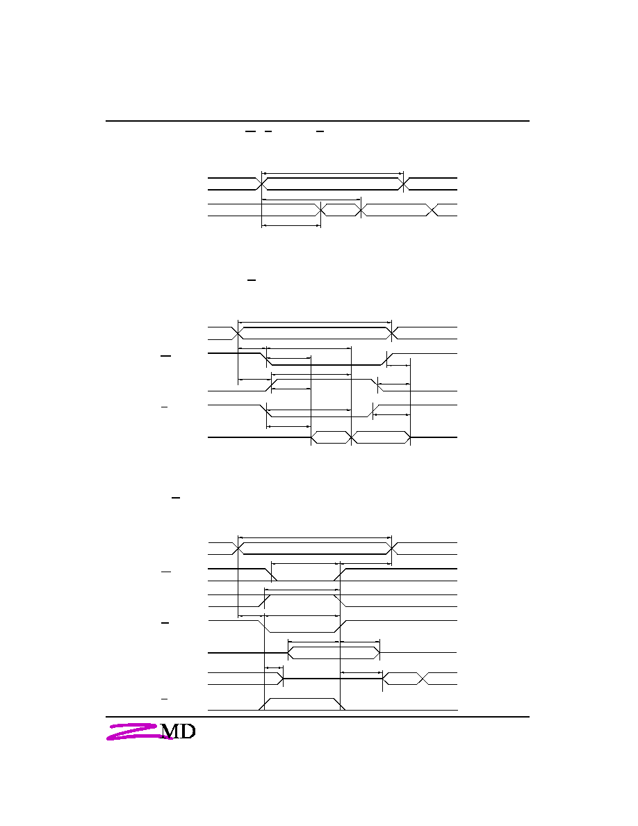
t
h(D)
Read Cycle 1 (during Read Cycle: E1 = G = V
IL
, E2 = W = V
IH
)
Read Cycle 2 (during Read Cycle: W = V
IH
)
Write Cycle 1 (W-controlled)
t
a(A)
Previous
Data Valid
Output Data
Valid
t
cR
Addresses Valid
t
v(A )
AAAA
AAAA
AAAA
AAAA
AAAA
AAAA
AAAA
AAAA
AAAA
AAAA
AAAA
AAAA
AAAA
AAAA
AAAA
AAAA
AAA
AAA
AAA
AAA
A
i
DQ
i
A
i
E1
E2
G
DQ
i
Output
Output
t
dis(E)
t
cR
t
su(A )
t
a(E)
t
su(A)
t
t(QX)
t
t(QX)
t
tG(QX)
t
a(G)
t
a(E)
t
dis(E)
t
dis(G)
Addresses Valid
Output Data
Valid
AAAA
AAAA
AAAA
AAAA
AAAA
AAAA
AAAA
AAAA
AAA
AAA
AAA
AAA
A
i
E1
E2
W
DQ
i
Input
G
DQ
i
Output
t
cW
t
su(E)
t
h(A )
t
w(W)
t
su(A )
t
su(E)
t
su(D)
t
dis(W)
t
t(QX)
Addresses Valid
Input Data
Valid
High-Z
AAAA
AAAA
AAAA
AAAA
AAAA
AAAA
AAAA
AAAA
AAAA
AAAA
AAAA
AAAA
AAAA
AAAA
AAAA
AAAA
AAAA
AAAA
AAAA
AAAA
AAAA
AAAA
AAAA
AAAA
AAAA
AAAA
AAAA
AAAA
AAAA
AAAA
AAAA
AAAA
AAAA
AAAA
AAAA
AAAA
AAAA
AAAA
AAAA
AAAA
AAAA
AAAA
AAAA
AAAA
AAAA
AAAA
AAAA
AAAA
AAAA
AAAA
AAAA
AAAA
AAAA
AAAA
AAAA
AAAA
AAAA
AAAA
AAAA
AAAA
AAAA
AAAA
AAAA
AAAA
AA
AA
AA
AA
AAAA
AAAA
AAAA
AAAA
AAAA
AAAA
AAAA
AAAA
AAA
AAA
AAA
AAA
AAAA
AAAA
AAAA
AAAA
AAAA
AAAA
AAAA
AAAA
AAAA
AAAA
AAAA
AAAA
AAAA
AAAA
AAAA
AAAA
AAAA
AAAA
AAAA
AAAA
AAAA
AAAA
AAAA
AAAA
AAAA
AAAA
AAAA
AAAA
AAAA
AAAA
AAAA
AAAA
AAAA
AAAA
AAAA
AAAA
AAAA
AAAA
AAAA
AAAA
AAAA
AAAA
AAAA
AAAA
AAAA
AAAA
AAAA
AAAA
AAAA
AAAA
AAAA
AAAA
AAA
AAA
AAA
AAA
7
December 12, 1997
UL6264A
High-Z
Input Data
Valid
t
h(D)
t
su(W)
t
w(E)
t
su(D)
t
cW
Addresses Valid
t
su(A )
t
su(E)
t
h(A )
t
t(QX)
t
dis(W)
AAAA
AAAA
AAAA
AAAA
AAAA
AAAA
AAAA
AAAA
AAAA
AAAA
AAAA
AAAA
AAAA
AAAA
AAAA
AAAA
AAAA
AAAA
AAAA
AAAA
AAAA
AAAA
AAAA
AAAA
AAAA
AAAA
AAAA
AAAA
AAAA
AAAA
AAAA
AAAA
AAAA
AAAA
AAAA
AAAA
AAAA
AAAA
AAAA
AAAA
AAAA
AAAA
AAAA
AAAA
AAAA
AAAA
AAAA
AAAA
AAAA
AAAA
AAAA
AAAA
AAAA
AAAA
AAAA
AAAA
AAAA
AAAA
AAAA
AAAA
AAAA
AAAA
AAAA
AAAA
AA
AA
AA
AA
AAAA
AAAA
AAAA
AAAA
AAAA
AAAA
AAAA
AAAA
AAAA
AAAA
AAAA
AAAA
AAAA
AAAA
AAAA
AAAA
AAAA
AAAA
AAAA
AAAA
AAAA
AAAA
AAAA
AAAA
AAAA
AAAA
AAAA
AAAA
AAAA
AAAA
AAAA
AAAA
AAAA
AAAA
AAAA
AAAA
AAAA
AAAA
AAAA
AAAA
AAAA
AAAA
AAAA
AAAA
AAA
AAA
AAA
AAA
AAAA
AAAA
AAAA
AAAA
AAAA
AAAA
AAAA
AAAA
AAAA
AAAA
AAAA
AAAA
AAAA
AAAA
AAAA
AAAA
AAAA
AAAA
AAAA
AAAA
AAAA
AAAA
AAAA
AAAA
AAAA
AAAA
AAAA
AAAA
AAAA
AAAA
AAAA
AAAA
A
i
E1
E2
W
DQ
i
Input
G
DQ
i
Output
t
su(A)
AAAA
AAAA
AAAA
AAAA
AAAA
AAAA
AAAA
AAAA
AAAA
AAAA
AAAA
AAAA
AAAA
AAAA
AAAA
A
A
A
A
A
AAAA
AAAA
AAAA
AAAA
AAAA
AAAA
AAAA
AAAA
AAAA
AAAA
AAAA
AAAA
AAAA
AAAA
AAAA
A
A
A
A
A
undefined L- or H-Level
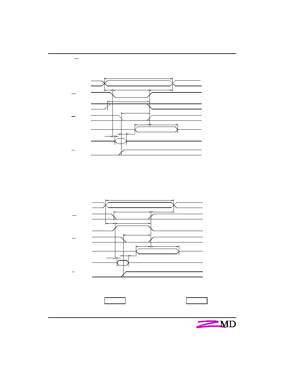
Write Cycle 2 (E1-controlled)
Write Cycle 3 (E2-controlled)
t
h(D)
A
i
E1
E2
W
DQ
i
Input
G
DQ
i
Output
t
cW
t
w(E)
t
h(A )
t
su(W)
t
su(E)
t
su(D)
t
dis(W)
t
t(QX )
Addresses Valid
Input Data
Valid
High-Z
AAAA
AAAA
AAAA
AAAA
AAAA
AAAA
AAAA
AAAA
AAAA
AAAA
AAAA
AAAA
AAAA
AAAA
AAAA
AAAA
AAAA
AAAA
AAAA
AAAA
AAAA
AAAA
AAAA
AAAA
AAAA
AAAA
AAAA
AAAA
AAAA
AAAA
AAAA
AAAA
AAAA
AAAA
AAAA
AAAA
AAAA
AAAA
AAAA
AAAA
AAAA
AAAA
AAAA
AAAA
AAAA
AAAA
AAAA
AAAA
AAAA
AAAA
AAAA
AAAA
AAAA
AAAA
AAAA
AAAA
AAAA
AAAA
AAAA
AAAA
AAAA
AAAA
AAAA
AAAA
AAA
AAA
AAA
AAA
AAAA
AAAA
AAAA
AAAA
AAAA
AAAA
AAAA
AAAA
AAAA
AAAA
AAAA
AAAA
AAAA
AAAA
AAAA
AAAA
AAAA
AAAA
AAAA
AAAA
AAAA
AAAA
AAAA
AAAA
AAAA
AAAA
AAAA
AAAA
AAAA
AAAA
AAAA
AAAA
AAAA
AAAA
AAAA
AAAA
AAAA
AAAA
AAAA
AAAA
AAAA
AAAA
AAAA
AAAA
AAAA
AAAA
AAAA
AAAA
AAAA
AAAA
AAAA
AAAA
AAAA
AAAA
AAAA
AAAA
AAAA
AAAA
AAAA
AAAA
AAAA
AAAA
AAAA
AAAA
AAAA
AAAA
AAAA
AAAA
AAAA
AAAA
AAAA
AAAA
AAAA
AAAA
AAAA
AAAA

LIFE SUPPORT POLICY
ZMD products are not designed, intended, or authorized for use as components in
systems intend for surgical implant into the body, or other applications intended to
support or sustain life, or for any other application in which the failure of the ZMD
product could create a situation where personal injury or death may occur.
Components used in life-support devices or systems must be expressly authorized
by ZMD for such purpose.
The information describes the type of component and shall not be considered as
assured characteristics.
Terms of delivery and rights to change design reserved.
Memory Products 1998
Low Voltage 8K x 8 SRAM UL6264A
Zentrum Mikroelektronik Dresden GmbH
Grenzstraþe 28
∑ D-01109 Dresden
∑
P.
O.
B. 80
01
34
∑
D-01101 Dresden
∑
Germany
Phone: +49 351 88 22-3 06 ∑ Fax: +49 351 88 22-3 37 ∑ Email: sales@zmd.de
Internet Web Site: http://www.zmd.de