UL635H256.fm
1
December 05, 2003
UL635H256
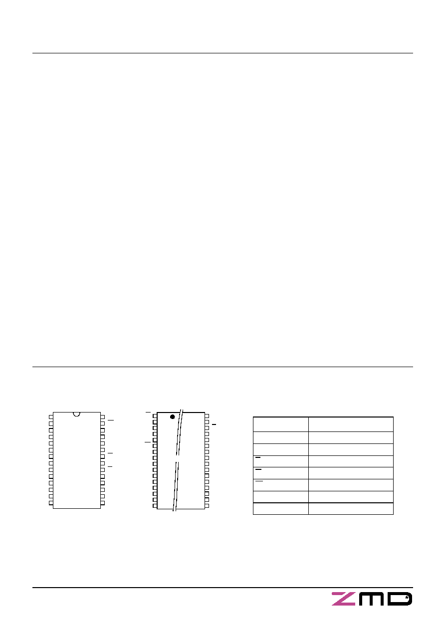
Pin Configuration
Pin Description
Signal Name
Signal Description
A0 - A14
Address Inputs
DQ0 - DQ7
Data In/Out
E
Chip Enable
G
Output Enable
W
Write Enable
VCC
Power Supply Voltage
VSS
Ground
G
A11
A9
A8
A13
W
n. c.
VCC
n. c.
A14
A12
A7
A6
A5
A4
A3
n.c.
A10
E
DQ7
DQ6
DQ5
DQ4
DQ3
VSS
DQ2
DQ1
DQ0
A0
A1
A2
n.c.
1
2
3
4
5
6
7
8
9
10
11
12
13
14
15
16
TSOP
Top View
32
31
30
29
28
27
26
25
24
23
22
21
20
19
18
17
A14
A12
A7
A6
A5
A4
A3
A2
A1
A0
DQ0
DQ1
DQ2
VSS
VCC
W
A13
A8
A9
A11
G
A10
E
DQ7
DQ6
DQ5
DQ4
DQ3
1
2
3
4
5
6
7
8
9
10
11
12
13
14
SOP
Top View
28
27
26
25
24
23
22
21
20
19
18
17
16
15
Low Voltage PowerStore 32K x 8 nvSRAM
!
High-performance CMOS non-
volatile static RAM 32768 x 8 bits
!
35 and 45 ns Access Times
!
15 and 20 ns Output Enable
Access Times
!
I
CC
= 8 mA typ. at 200 ns Cycle
Time
!
Automatic STORE to EEPROM
on Power Down using system
capacitance
!
Software initiated STORE
!
Automatic STORE Timing
!
10
5
STORE cycles to EEPROM
!
10 years data retention in
EEPROM
!
Automatic RECALL on Power Up
!
Software RECALL Initiation
!
Unlimited RECALL cycles from
EEPROM
!
Wide voltage range: 2.7 ... 3.6 V
(3.0 ... 3.6 V for 35 ns type)
!
Operating temperature range:
0 to 70 �C
-40 to 85 �C
!
QS 9000 Quality Standard
!
ESD protection > 2000 V
(MIL STD 883C M3015.7-HBM)
!
Packages: SOP28 (330 mil)
TSOP32 (Type I)
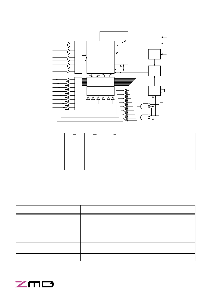
The UL635H256 has two separate
modes of operation: SRAM mode
and nonvolatile mode. In SRAM
mode, the memory operates as an
ordinary static RAM. In nonvolatile
operation, data is transferred in
parallel from SRAM to EEPROM or
from EEPROM to SRAM. In this
mode SRAM functions are disab-
led.
The UL635H256 is a fast static
RAM (35 and 45 ns), with a nonvo-
latile electrically erasable PROM
(EEPROM) element incorporated
in each static memory cell. The
SRAM can be read and written an
unlimited number of times, while
independent nonvolatile data resi-
des in EEPROM. Data transfers
from the SRAM to the EEPROM
(the STORE operation) take place
automatically upon power down
using charge stored in system
capacitance. Transfers from the
EEPROM to the SRAM (the
RECALL operation) take place
automatically on powerup.
The UL635H256 combines the
high performance and ease of use
of a fast SRAM with nonvolatile
data integrity.
STORE cycles also may be initia-
ted under user control via a soft-
ware sequence.
Once a STORE cycle is initiated,
further input or output are disabled
until the cycle is completed.
Because a sequence of addresses
is used for STORE initiation, it is
important that no other read or
write accesses intervene in the
sequence or the sequence will be
aborted.
RECALL cycles may also be initia-
ted by a software sequence.
Internally, RECALL is a two step
procedure. First, the SRAM data is
cleared and second, the nonvola-
tile information is transferred into
the SRAM cells.
The RECALL operation in no way
alters the data in the EEPROM
cells. The nonvolatile data can be
recalled an unlimited number of
times.
Features
Description
2
December 05, 2003
UL635H256
EEPROM Array
512 x (64 x 8)
RECALL
DQ0
DQ1
DQ2
DQ3
DQ4
DQ5
DQ6
DQ7
Column I/O
Column Decoder
A0 - A13
Store/
Recall
Control
Ro
w De
c
o
d
e
r
V
CC
V
SS
G
E
W
A0 A1
A2
A3
A4 A10
Software
Detect
Power
Control
V
CC
A5
A6
A7
A8
A9
A11
A12
A13
A14
In
p
u
t
Bu
f
f
e
r
s
STORE
SRAM
Array
512 Rows x
64 x 8 Columns
Block Diagram
Truth Table for SRAM Operations
Operating Mode
E
W
G
DQ0 - DQ7
Standby/not selected
H
*
*
High-Z
Internal Read
L
H
H
High-Z
Read
L
H
L
Data Outputs Low-Z
Write
L
L
*
Data Inputs High-Z
*
H or L
Characteristics
All voltages are referenced to V
SS
= 0 V (ground).
All characteristics are valid in the power supply voltage range and in the operating temperature range specified.
Dynamic measurements are based on a rise and fall time of
5 ns, measured between 10 % and 90 % of V
I
, as well as
input levels of V
IL
= 0 V and V
IH
= 3 V. The timing reference level of all input and output signals is 1.5 V,
with the exception of the t
dis
-times and t
en
-times, in which cases transition is measured
� 200 mV from steady-state voltage.
a: Stresses greater than those listed under ,,Absolute Maximum Ratings" may cause permanent damage to the device. This is a stress
rating only, and functional operation of the device at condition above those indicated in the operational sections of this specification is
not implied. Exposure to absolute maximum rating conditions for extended periods may affect reliability.
Absolute Maximum Ratings
a
Symbol
Min.
Max.
Unit
Power Supply Voltage
V
CC
-0.5
4.6
V
Input Voltage
V
I
-0.3
V
CC
+0.5
V
Output Voltage
V
O
-0.3
V
CC
+0.5
V
Power Dissipation
P
D
1
W
Operating Temperature
C-Type
K-Type
T
a
0
-40
70
85
�C
�C
Storage Temperature
T
stg
-65
150
�C
3
December 05, 2003
UL635H256
b: I
CC1
and I
CC3
are depedent on output loading and cycle rate. The specified values are obtained with outputs unloaded.
The current I
CC1
is measured for WRITE/READ - ratio of 1/2.
c: I
CC2
and I
CC4
are the average currents required for the duration of the respective STORE cycles.
d: Bringing E
V
IH
will not produce standby current levels until any nonvolatile cycle in progress has timed out. See MODE SELECTION
table. The current I
CC(SB)1
is measured for WRITE/READ - ratio of 1/2.
DC Characteristics
Symbol
Conditions
C-Type
K-Type
Unit
Min.
Max.
Min.
Max.
Operating Supply Current
b
I
CC1
V
CC
V
IL
V
IH
t
c
t
c
= 3.6 V
= 0.8 V
= 2.2 V
= 35 ns
= 45 ns
45
35
47
37
mA
mA
Average Supply Current during
c
STORE
I
CC2
V
CC
E
W
V
IL
V
IH
= 3.6 V
0.2 V
V
CC
-0.2 V
0.2 V
V
CC
-0.2 V
3
4
mA
Operating Supply Current
b
at t
cR
= 200 ns
(Cycling CMOS Input Levels)
I
CC3
V
CC
W
V
IL
V
IH
= 3.6 V
V
CC
-0.2 V
0.2 V
V
CC
-0.2 V
10
11
mA
Average Supply Current during
c
PowerStore Cycle
I
CC4
V
CC
V
IL
V
IH
= V
CCmin
= 0.2 V
V
CC
-0.2 V
2
2
mA
Standby Supply Current
d
(Cycling TTL Input Levels)
I
CC(SB)1
V
CC
E
t
c
t
c
= 3.6 V
= V
IH
= 35 ns
= 45 ns
11
9
12
10
mA
mA
Standby Supply Curent
d
(Stable CMOS Input Levels)
I
CC(SB)
V
CC
E
V
IL
V
IH
= 3.6 V
V
CC
-0.2 V
0.2 V
V
CC
-0.2 V
1
1
mA
Recommended
Operating Conditions
Symbol
Conditions
Min.
Max.
Unit
Power Supply Voltage
V
CC
t
c
= 35 ns
t
c
= 45 ns
3.0
2.7
3.6
3.6
V
V
Input Low Voltage
V
IL
-2 V at Pulse Width
10 ns permitted
-0.3
0.8
V
Input High Voltage
V
IH
2.2
V
CC
+0.3
V
4
December 05, 2003
UL635H256
DC Characteristics
Symbol
Conditions
C-Type
K-Type
Unit
Min.
Max.
Min.
Max.
Output High Voltage
Output Low Voltage
V
OH
V
OL
V
CC
I
OH
I
OL
= V
CC
min
=-2 mA
= 2 mA
2.4
0.4
2.4
0.4
V
V
Output High Current
Output Low Current
I
OH
I
OL
V
CC
V
OH
V
OL
= V
CC
min
= 2.4 V
= 0.4 V
2
-2
2
-2
mA
mA
Input Leakage Current
High
Low
I
IH
I
IL
V
CC
V
IH
V
IL
= 3.6 V
= 3.6 V
= 0 V
-1
1
-1
1
�A
�A
Output Leakage Current
High at Three-State- Output
Low at Three-State- Output
I
OHZ
I
OLZ
V
CC
V
OH
V
OL
= 3.6 V
= 3.6 V
= 0 V
-1
1
-1
1
�A
�A
SRAM Memory Operations
No.
Switching Characteristics
Read Cycle
Symbol
35
45
Unit
Alt.
IEC
Min.
Max.
Min.
Max.
1
Read Cycle Time
f
t
AVAV
t
cR
35
45
ns
2
Address Access Time to Data Valid
g
t
AVQV
t
a(A)
35
45
ns
3
Chip Enable Access Time to Data Valid
t
ELQV
t
a(E)
35
45
ns
4
Output Enable Access Time to Data
Valid
t
GLQV
t
a(G)
15
20
ns
5
E HIGH to Output in High-Z
h
t
EHQZ
t
dis(E)
13
15
ns
6
G HIGH to Output in High-Z
h
t
GHQZ
t
dis(G)
13
15
ns
7
E LOW to Output in Low-Z
t
ELQX
t
en(E)
5
5
ns
8
G LOW to Output in Low-Z
t
GLQX
t
en(G)
0
0
ns
9
Output Hold Time after Address Change
t
AXQX
t
v(A)
3
3
ns
10 Chip Enable to Power Active
e
t
ELICCH
t
PU
0
0
ns
11 Chip Disable to Power Standby
d, e
t
EHICCL
t
PD
35
45
ns
e: Parameter guaranteed but not tested.
f:
Device is continuously selected with E and G both Low.
g: Address valid prior to or coincident with E transition LOW.
h: Measured
� 200 mV from steady state output voltage.
5
December 05, 2003
UL635H256
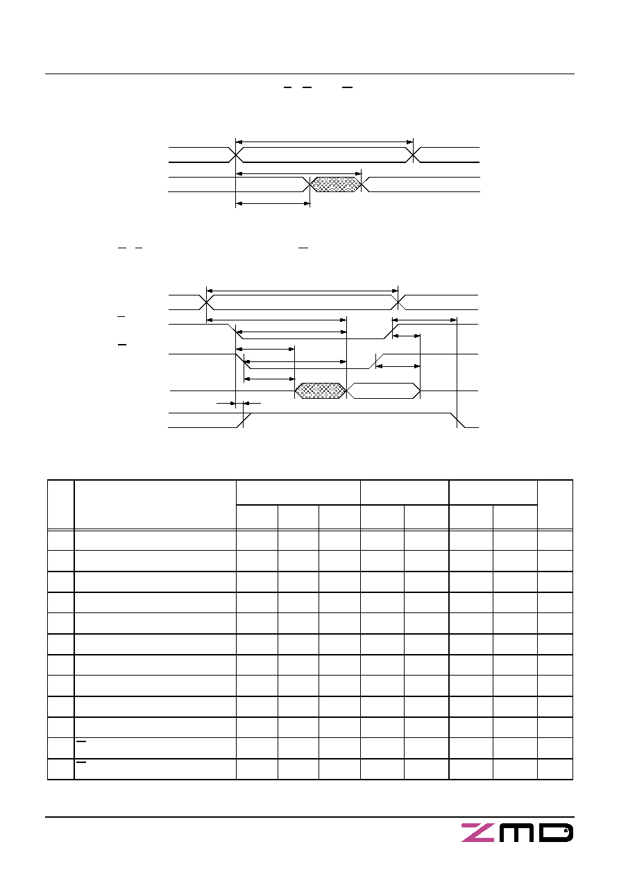
Read Cycle 1: Ai-controlled (during Read cycle: E = G = V
IL
, W = V
IH
)
f
No.
Switching Characteristics
Write Cycle
Symbol
35
45
Unit
Alt. #1 Alt. #2
IEC
Min.
Max.
Min.
Max.
12 Write Cycle Time
t
AVAV
t
AVAV
t
cW
35
45
ns
13 Write Pulse Width
t
WLWH
t
w(W)
25
30
ns
14 Write Pulse Width Setup Time
t
WLEH
t
su(W)
25
30
ns
15 Address Setup Time
t
AVWL
t
AVEL
t
su(A)
0
0
ns
16 Address Valid to End of Write
t
AVWH
t
AVEH
t
su(A-WH)
25
30
ns
17 Chip Enable Setup Time
t
ELWH
t
su(E)
25
30
ns
18 Chip Enable to End of Write
t
ELEH
t
w(E)
25
30
ns
19 Data Setup Time to End of Write
t
DVWH
t
DVEH
t
su(D)
12
15
ns
20 Data Hold Time after End of Write
t
WHDX
t
EHDX
t
h(D)
0
0
ns
21 Address Hold after End of Write
t
WHAX
t
EHAX
t
h(A)
0
0
ns
22 W LOW to Output in High-Z
h, i
t
WLQZ
t
dis(W)
13
15
ns
23 W HIGH to Output in Low-Z
t
WHQX
t
en(W)
5
5
ns
Read Cycle 2: G-, E-controlled (during Read cycle: W = V
IH
)
g
t
a(A)
Previous Data Valid
Output Data Valid
t
cR
Address Valid
t
v(A)
Ai
DQi
Output
(1)
(2)
(9)
Ai
E
G
DQi
Output
t
dis(E)
t
cR
t
a(E)
t
en(E)
t
en(G)
t
a(G)
t
dis(G)
Output Data Valid
High Impedance
I
CC
ACTIVE
STANDBY
t
PD
t
PU
(1)
(3)
(4)
(5)
(7)
(6)
(8)
(10)
(11)
t
a(A)
(2)
Address Valid
DQi
Output